JP2011118300A - Display device, driving method of the same, and electronic equipment - Google Patents
Display device, driving method of the same, and electronic equipmentDownload PDFInfo
- Publication number
- JP2011118300A JP2011118300AJP2009277813AJP2009277813AJP2011118300AJP 2011118300 AJP2011118300 AJP 2011118300AJP 2009277813 AJP2009277813 AJP 2009277813AJP 2009277813 AJP2009277813 AJP 2009277813AJP 2011118300 AJP2011118300 AJP 2011118300A
- Authority
- JP
- Japan
- Prior art keywords
- light emitting
- display
- emitting element
- pixel
- transistor
- Prior art date
- Legal status (The legal status is an assumption and is not a legal conclusion. Google has not performed a legal analysis and makes no representation as to the accuracy of the status listed.)
- Pending
Links
- 238000000034methodMethods0.000titleclaimsabstractdescription12
- 239000003990capacitorSubstances0.000description7
- 238000007789sealingMethods0.000description6
- 230000004048modificationEffects0.000description5
- 238000012986modificationMethods0.000description5
- 238000009616inductively coupled plasmaMethods0.000description3
- 235000010384tocopherolNutrition0.000description3
- 235000019731tricalcium phosphateNutrition0.000description3
- 238000006073displacement reactionMethods0.000description2
- 230000000694effectsEffects0.000description2
- 239000011521glassSubstances0.000description2
- 239000004973liquid crystal related substanceSubstances0.000description2
- 230000001902propagating effectEffects0.000description2
- 229920006395saturated elastomerPolymers0.000description2
- 239000000758substrateSubstances0.000description2
- 101000702394Homo sapiens Signal peptide peptidase-like 2AProteins0.000description1
- 238000010586diagramMethods0.000description1
- 230000005611electricityEffects0.000description1
- 238000005401electroluminescenceMethods0.000description1
- 239000011159matrix materialSubstances0.000description1
- 239000000203mixtureSubstances0.000description1
- 230000003287optical effectEffects0.000description1
- 238000010791quenchingMethods0.000description1
- 230000000171quenching effectEffects0.000description1
- 239000010409thin filmSubstances0.000description1
Images


Classifications
- G—PHYSICS
- G09—EDUCATION; CRYPTOGRAPHY; DISPLAY; ADVERTISING; SEALS
- G09G—ARRANGEMENTS OR CIRCUITS FOR CONTROL OF INDICATING DEVICES USING STATIC MEANS TO PRESENT VARIABLE INFORMATION
- G09G3/00—Control arrangements or circuits, of interest only in connection with visual indicators other than cathode-ray tubes
- G09G3/20—Control arrangements or circuits, of interest only in connection with visual indicators other than cathode-ray tubes for presentation of an assembly of a number of characters, e.g. a page, by composing the assembly by combination of individual elements arranged in a matrix no fixed position being assigned to or needed to be assigned to the individual characters or partial characters
- G09G3/22—Control arrangements or circuits, of interest only in connection with visual indicators other than cathode-ray tubes for presentation of an assembly of a number of characters, e.g. a page, by composing the assembly by combination of individual elements arranged in a matrix no fixed position being assigned to or needed to be assigned to the individual characters or partial characters using controlled light sources
- G09G3/30—Control arrangements or circuits, of interest only in connection with visual indicators other than cathode-ray tubes for presentation of an assembly of a number of characters, e.g. a page, by composing the assembly by combination of individual elements arranged in a matrix no fixed position being assigned to or needed to be assigned to the individual characters or partial characters using controlled light sources using electroluminescent panels
- G09G3/32—Control arrangements or circuits, of interest only in connection with visual indicators other than cathode-ray tubes for presentation of an assembly of a number of characters, e.g. a page, by composing the assembly by combination of individual elements arranged in a matrix no fixed position being assigned to or needed to be assigned to the individual characters or partial characters using controlled light sources using electroluminescent panels semiconductive, e.g. using light-emitting diodes [LED]
- G09G3/3208—Control arrangements or circuits, of interest only in connection with visual indicators other than cathode-ray tubes for presentation of an assembly of a number of characters, e.g. a page, by composing the assembly by combination of individual elements arranged in a matrix no fixed position being assigned to or needed to be assigned to the individual characters or partial characters using controlled light sources using electroluminescent panels semiconductive, e.g. using light-emitting diodes [LED] organic, e.g. using organic light-emitting diodes [OLED]
- G09G3/3225—Control arrangements or circuits, of interest only in connection with visual indicators other than cathode-ray tubes for presentation of an assembly of a number of characters, e.g. a page, by composing the assembly by combination of individual elements arranged in a matrix no fixed position being assigned to or needed to be assigned to the individual characters or partial characters using controlled light sources using electroluminescent panels semiconductive, e.g. using light-emitting diodes [LED] organic, e.g. using organic light-emitting diodes [OLED] using an active matrix
- G09G3/3233—Control arrangements or circuits, of interest only in connection with visual indicators other than cathode-ray tubes for presentation of an assembly of a number of characters, e.g. a page, by composing the assembly by combination of individual elements arranged in a matrix no fixed position being assigned to or needed to be assigned to the individual characters or partial characters using controlled light sources using electroluminescent panels semiconductive, e.g. using light-emitting diodes [LED] organic, e.g. using organic light-emitting diodes [OLED] using an active matrix with pixel circuitry controlling the current through the light-emitting element
- G—PHYSICS
- G09—EDUCATION; CRYPTOGRAPHY; DISPLAY; ADVERTISING; SEALS
- G09G—ARRANGEMENTS OR CIRCUITS FOR CONTROL OF INDICATING DEVICES USING STATIC MEANS TO PRESENT VARIABLE INFORMATION
- G09G2300/00—Aspects of the constitution of display devices
- G09G2300/08—Active matrix structure, i.e. with use of active elements, inclusive of non-linear two terminal elements, in the pixels together with light emitting or modulating elements
- G09G2300/0809—Several active elements per pixel in active matrix panels
- G09G2300/0842—Several active elements per pixel in active matrix panels forming a memory circuit, e.g. a dynamic memory with one capacitor
- G—PHYSICS
- G09—EDUCATION; CRYPTOGRAPHY; DISPLAY; ADVERTISING; SEALS
- G09G—ARRANGEMENTS OR CIRCUITS FOR CONTROL OF INDICATING DEVICES USING STATIC MEANS TO PRESENT VARIABLE INFORMATION
- G09G2320/00—Control of display operating conditions
- G09G2320/02—Improving the quality of display appearance
- G09G2320/029—Improving the quality of display appearance by monitoring one or more pixels in the display panel, e.g. by monitoring a fixed reference pixel
- G—PHYSICS
- G09—EDUCATION; CRYPTOGRAPHY; DISPLAY; ADVERTISING; SEALS
- G09G—ARRANGEMENTS OR CIRCUITS FOR CONTROL OF INDICATING DEVICES USING STATIC MEANS TO PRESENT VARIABLE INFORMATION
- G09G2330/00—Aspects of power supply; Aspects of display protection and defect management
- G09G2330/02—Details of power systems and of start or stop of display operation
- G09G2330/021—Power management, e.g. power saving
- G—PHYSICS
- G09—EDUCATION; CRYPTOGRAPHY; DISPLAY; ADVERTISING; SEALS
- G09G—ARRANGEMENTS OR CIRCUITS FOR CONTROL OF INDICATING DEVICES USING STATIC MEANS TO PRESENT VARIABLE INFORMATION
- G09G2330/00—Aspects of power supply; Aspects of display protection and defect management
- G09G2330/08—Fault-tolerant or redundant circuits, or circuits in which repair of defects is prepared
Landscapes
- Engineering & Computer Science (AREA)
- Physics & Mathematics (AREA)
- Computer Hardware Design (AREA)
- General Physics & Mathematics (AREA)
- Theoretical Computer Science (AREA)
- Electroluminescent Light Sources (AREA)
- Control Of El Displays (AREA)
- Control Of Indicators Other Than Cathode Ray Tubes (AREA)
Abstract
Description
Translated fromJapanese本発明は、表示パネルに発光素子が設けられた表示装置およびその駆動方法に関する。また、本発明は、上記表示装置を備えた電子機器に関する。 The present invention relates to a display device in which a light emitting element is provided on a display panel and a driving method thereof. Moreover, this invention relates to the electronic device provided with the said display apparatus.
近年、画像表示を行う表示装置の分野では、画素の発光素子として、流れる電流値に応じて発光輝度が変化する電流駆動型の光学素子、例えば有機EL(electro luminescence)素子を用いた表示装置が開発され、商品化が進められている。有機EL素子は、液晶素子などと異なり自発光素子である。そのため、有機EL素子を用いた表示装置(有機EL表示装置)では、光源(バックライト)が必要ないので、光源を必要とする液晶表示装置と比べて、薄型化、高輝度化することができる。特に、駆動方式としてアクティブマトリクス方式を用いた場合には、各画素をホールド点灯させることができ、低消費電力化することもできる。そのため、有機EL表示装置は、次世代のフラットパネルディスプレイの主流になると期待されている。 In recent years, in the field of display devices that perform image display, display devices that use current-driven optical elements, such as organic EL (electroluminescence) elements, whose light emission luminance changes according to the value of a flowing current are used as light emitting elements of pixels. Developed and commercialized. Unlike a liquid crystal element or the like, the organic EL element is a self-luminous element. Therefore, a display device (organic EL display device) using an organic EL element does not require a light source (backlight), so that it can be made thinner and brighter than a liquid crystal display device that requires a light source. . In particular, when the active matrix method is used as the driving method, each pixel can be lighted on hold and power consumption can be reduced. Therefore, organic EL display devices are expected to become the mainstream of next-generation flat panel displays.
有機EL素子は、電流駆動型の発光素子であり、有機EL素子に流れる電流量を制御することにより階調を調整することの可能な素子である。しかし、有機EL素子は、通電時間や素子温度に応じてI−V特性が変化する性質を有している。そのため、I−V特性が経時的に変化した場合であっても一定の輝度を得ることができるようにするために、有機EL素子に流れる電流量を制御する駆動トランジスタは常に飽和領域で駆動される(特許文献1参照)。 The organic EL element is a current-driven light-emitting element, and is an element capable of adjusting gradation by controlling the amount of current flowing through the organic EL element. However, the organic EL element has a property that the IV characteristic changes according to the energization time and the element temperature. For this reason, the drive transistor for controlling the amount of current flowing in the organic EL element is always driven in the saturation region in order to obtain a constant luminance even when the IV characteristic changes over time. (See Patent Document 1).
ところで、有機EL素子のI−V特性が経時的に変動する状況下で、駆動トランジスタを常に飽和領域で駆動させるためには、電源電圧を、有機EL素子のI−V特性が変動したときに駆動トランジスタが線形駆動とはならない程度に十分に高い値に設定しておくことが必要となる。例えば、有機EL素子のI−V特性の変動によって有機EL素子の端子間電圧が2V程度大きくなることが予想される場合には、あらかじめ、電源電圧を、2V程度の余裕を持った電圧値に設定することが考えられる。しかし、電源電圧のマージンを予測に基づいて設定した場合には、電源電圧が、駆動トランジスタを常に飽和領域で駆動させるのに必要な最低限の電圧よりも大きくなり易く、余分に見積もった電圧の分だけ消費電力が高くなってしまうという問題があった。 By the way, in order to always drive the drive transistor in the saturation region under the situation where the IV characteristic of the organic EL element fluctuates with time, the power supply voltage is changed when the IV characteristic of the organic EL element fluctuates. It is necessary to set the driving transistor to a sufficiently high value so that the driving transistor is not linearly driven. For example, when the voltage between the terminals of the organic EL element is expected to increase by about 2V due to fluctuations in the IV characteristics of the organic EL element, the power supply voltage is set to a voltage value with a margin of about 2V in advance. It is possible to set. However, when the power supply voltage margin is set based on the prediction, the power supply voltage tends to be larger than the minimum voltage required to drive the drive transistor in the saturation region at all times. There was a problem that the power consumption increased by the amount.
本発明はかかる問題点に鑑みてなされたものであり、その目的は、消費電力を低く抑えることの可能な表示装置およびその駆動方法ならびに電子機器を提供することにある。 The present invention has been made in view of such problems, and an object of the present invention is to provide a display device that can reduce power consumption, a driving method thereof, and an electronic apparatus.
本発明による表示装置は、第1発光素子を含む複数の表示画素が2次元配置された表示領域と、第2発光素子を含む1または複数の調整用画素が配置された非表示領域とを有する表示部を備えたものである。この表示装置は、さらに、映像信号に基づいて各表示画素を駆動すると共に、第2発光素子に定電流を印加する駆動部を備えている。ここで、駆動部は、第2発光素子の電圧変動に応じた値の電源電圧を各表示画素に印加するようになっている。 A display device according to the present invention includes a display region in which a plurality of display pixels including a first light emitting element are two-dimensionally arranged, and a non-display region in which one or a plurality of adjustment pixels including a second light emitting element are disposed. A display unit is provided. The display device further includes a drive unit that drives each display pixel based on the video signal and applies a constant current to the second light emitting element. Here, the drive unit applies a power supply voltage having a value corresponding to the voltage fluctuation of the second light emitting element to each display pixel.
本発明による電子機器は、上記表示装置を備えたものである。 An electronic apparatus according to the present invention includes the display device.
本発明による表示装置の駆動方法は、第1発光素子を含む複数の表示画素が2次元配置された表示領域と、第2発光素子を含む1または複数の調整用画素が配置された非表示領域とを有する表示部と、映像信号に基づいて各表示画素を駆動すると共に、第2発光素子に定電流を印加する駆動部とを備えた表示装置において、以下のステップを含むものである。
(1)第2発光素子の電圧変動に応じた値の電源電圧を各表示画素に印加するステップA display device driving method according to the present invention includes a display region in which a plurality of display pixels including a first light emitting element are two-dimensionally arranged, and a non-display region in which one or a plurality of adjustment pixels including a second light emitting element are disposed. A display device that includes: a display unit that drives each display pixel based on a video signal, and applies a constant current to the second light emitting element, includes the following steps.
(1) A step of applying a power supply voltage having a value corresponding to the voltage fluctuation of the second light emitting element to each display pixel.
本発明による表示装置およびその駆動方法ならびに電子機器では、調整用画素に含まれる第2発光素子に定電流が印加され、第2発光素子の電圧変動に応じた値の電源電圧が各表示画素に印加される。これにより、電源電圧のマージンを予測に基づいて設定した場合と比べて、定電流を流すのに要する電源電圧の値を小さく設定することができる。 In the display device, the driving method thereof, and the electronic apparatus according to the present invention, a constant current is applied to the second light emitting element included in the adjustment pixel, and a power supply voltage having a value corresponding to the voltage variation of the second light emitting element is applied to each display pixel. Applied. Thereby, compared with the case where the margin of a power supply voltage is set based on prediction, the value of the power supply voltage required to flow a constant current can be set small.
本発明による表示装置およびその駆動方法ならびに電子機器によれば、電源電圧のマージンを予測に基づいて設定した場合と比べて、定電流を流すのに要する電源電圧の値を小さく設定することができるようにした。これにより、消費電力を低く抑えることができる。 According to the display device, the driving method thereof, and the electronic apparatus according to the present invention, the value of the power supply voltage required to flow a constant current can be set smaller than when the power supply voltage margin is set based on prediction. I did it. Thereby, power consumption can be kept low.
以下、発明を実施するための形態について、図面を参照して詳細に説明する。なお、説明は以下の順序で行う。
1.第1の実施の形態(図1〜図10)
2.第1の実施の形態の変形例(図11〜図12)
3.第2の実施の形態(図13〜図15)
4.第2の実施の形態の変形例(図16、図17)
5.第1および第2の実施の形態に共通する変形例(図なし)
6.適用例(図18〜図22)
DESCRIPTION OF EMBODIMENTS Hereinafter, embodiments for carrying out the invention will be described in detail with reference to the drawings. The description will be given in the following order.
1. 1st Embodiment (FIGS. 1-10)
2. Modified example of the first embodiment (FIGS. 11 to 12)
3. Second embodiment (FIGS. 13 to 15)
4). Modified example of the second embodiment (FIGS. 16 and 17)
5. Modification common to the first and second embodiments (not shown)
6). Application examples (FIGS. 18 to 22)
<第1の実施の形態>
(表示装置1の概略構成)
図1は、本発明の第1の実施の形態に係る表示装置1の概略構成を表したものである。この表示装置1は、表示パネル10(表示部)と、表示パネル10を駆動する駆動回路20(駆動部)とを備えている。<First Embodiment>
(Schematic configuration of the display device 1)
FIG. 1 shows a schematic configuration of a
表示パネル10は、複数の有機EL素子11R,11G,11B(第1発光素子)が2次元配置された表示領域10Aを有している。なお、以下では、有機EL素子11R,11G,11Bの総称として有機EL素子11を適宜、用いるものとする。表示パネル10は、また、有機EL素子12(第2発光素子)が配置された非表示領域10Bを有している。有機EL素子12は、有機EL素子11R,11G,11Bのいずれか1つと同一の発光色で発光する有機EL素子、または、有機EL素子11R,11G,11Bの発光色とは異なる発光色で発光する有機EL素子(例えば、白色光を発光する有機EL素子)である。 The
駆動回路20は、タイミング生成回路21、映像信号処理回路22、信号線駆動回路23、書込線駆動回路24、電源線駆動回路25、調整用画素駆動回路26および電源電圧調整回路27を有している。 The
(表示画素15)
図2は、表示領域10A内の回路構成の一例を表したものである。表示領域10A内には、複数の画素回路13が個々の有機EL素子11と対となって2次元配置されている。なお、本実施の形態では、一対の有機EL素子11および画素回路13が1つのサブピクセル14を構成している。より詳細には、図1に示したように、一対の有機EL素子11Rおよび画素回路13が1つのサブピクセル14Rを構成し、一対の有機EL素子11Gおよび画素回路13が1つのサブピクセル14Gを構成し、一対の有機EL素子11Bおよび画素回路13が1つのサブピクセル14Bを構成している。さらに、互いに隣り合う3つのサブピクセル14R,14G,14Bが1つの画素(表示画素15)を構成している。(Display pixel 15)
FIG. 2 shows an example of a circuit configuration in the
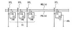
各画素回路13は、例えば、駆動トランジスタTr1(第1トランジスタ)、書き込みトランジスタTr2(第2トランジスタ)および保持容量Cs1によって構成されたものであり、2Tr1Cの回路構成となっている。駆動トランジスタTr1および書き込みトランジスタTr2は、例えば、nチャネルMOS型の薄膜トランジスタ(TFT(Thin Film Transistor))により形成されている。駆動トランジスタTr1または書き込みトランジスタTr2は、例えば、pチャネルMOS型のTFTであってもよい。Each
表示領域10Aにおいて、列方向には信号線DTLが複数配置され、行方向には書込線WSLおよび電源線PSL(電源電圧の供給される部材)がそれぞれ複数配置されている。各信号線DTLと各書込線WSLとの交差点近傍には、有機EL素子11が1つずつ設けられている。各信号線DTLは、信号線駆動回路23の出力端(図示せず)と、書き込みトランジスタTr2のドレイン電極およびソース電極のいずれか一方(図示せず)に接続されている。各書込線WSLは、書込線駆動回路24の出力端(図示せず)と、書き込みトランジスタTr2のゲート電極(図示せず)に接続されている。各電源線PSLは、電源線駆動回路25の出力端(図示せず)と、駆動トランジスタTr1のドレイン電極およびソース電極のいずれか一方(図示せず)に接続されている。書き込みトランジスタTr2のドレイン電極およびソース電極のうち信号線DTLに非接続の方(図示せず)は、駆動トランジスタTr1のゲート電極(図示せず)と、保持容量Cs1の一端に接続されている。駆動トランジスタTr1のドレイン電極およびソース電極のうち電源線PSLに非接続の方(図示せず)と保持容量Cs1の他端とが、有機EL素子11のアノード電極(図示せず)に接続されている。有機EL素子11のカソード電極(図示せず)は、例えば、グラウンド線GNDに接続されている。In
(調整用画素17)
図3は、非表示領域10B内の回路構成の一例を表したものである。非表示領域10B内には、調整用画素17が設けられている。この調整用画素17は、例えば、図3に示したように、1つの有機EL素子12を含んで構成されている。有機EL素子12のアノード電極(図示せず)は、電流信号線CSLおよびアノード信号線ASLのそれぞれの一端に接続されている。有機EL素子12のカソード電極(図示せず)は、例えば、グラウンド線GNDに接続されている。(Adjustment pixel 17)
FIG. 3 illustrates an example of a circuit configuration in the
(表示パネル10の上面構成)
図4は、表示パネル10の上面構成の一例を表したものである。表示パネル10は、例えば、駆動パネル30と封止パネル40とが封止層(図示せず)を介して貼り合わされた構造となっている。(Top panel configuration of display panel 10)
FIG. 4 illustrates an example of a top surface configuration of the
駆動パネル30は、図4には示していないが、表示領域10Aに、2次元配置された複数の有機EL素子11と、各有機EL素子11に隣接して配置された複数の画素回路13とを有している。駆動パネル30は、また、図4には示していないが、非表示領域10Bに、1つの有機EL素子12を有している。 Although not shown in FIG. 4, the
駆動パネル30の一辺(長辺)には、例えば、図4に示したように、複数の映像信号供給TAB51と、信号入出力TCP54が取り付けられている。駆動パネル30の他の辺(短辺)には、例えば、走査信号供給TAB52が取り付けられている。また、駆動パネル30の短辺であって、かつ走査信号供給TAB52とは異なる辺には、例えば、電源電圧供給TAB53が取り付けられている。映像信号供給TAB51は、信号線駆動回路23の集積されたICをフィルム状の配線基板の開口に中空配線したものである。走査信号供給TAB52は、書込線駆動回路24の集積されたICをフィルム状の配線基板の開口に中空配線したものである。電源電圧供給TAB53は、電源線駆動回路25の集積されたICをフィルム状の配線基板の開口に中空配線したものである。電源電圧供給TAB53は、電源電圧調整回路27の出力端(図示せず)に接続されている。信号入出力TCP54は、電源電圧調整回路27の入力端(図示せず)に接続されている。なお、信号線駆動回路23、書込線駆動回路24および電源線駆動回路25は、TABに形成されていなくてもよく、例えば、駆動パネル30に形成されていてもよい。 For example, as shown in FIG. 4, a plurality of video
封止パネル40は、例えば、有機EL素子11,12を封止する封止基板(図示せず)と、カラーフィルタ(図示せず)とを有している。カラーフィルタは、例えば、封止基板の表面のうち有機EL素子11の光が通過する領域に設けられている。カラーフィルタは、例えば、有機EL素子11R,11G,11Bのそれぞれに対応して、赤色用のフィルタ、緑色用のフィルタおよび青色用のフィルタ(図示せず)を有している。 The sealing
(駆動回路20)
次に、駆動回路20内の各回路について、図1を参照して説明する。タイミング生成回路21は、映像信号処理回路22、信号線駆動回路23、書込線駆動回路24、電源線駆動回路25、調整用画素駆動回路26および電源電圧調整回路27が連動して動作するように制御するものである。(Drive circuit 20)
Next, each circuit in the
タイミング生成回路21は、例えば、外部から入力された同期信号20Bに応じて(同期して)、上述した各回路に対して制御信号21Aを出力するようになっている。タイミング生成回路21は、例えば、映像信号処理回路22および電源電圧調整回路27などと共に、例えば、表示パネル10とは別体の制御回路基板(図示せず)上に形成されている。 The
映像信号処理回路22は、例えば、外部から入力された同期信号20Bに応じて(同期して)、外部から入力されたデジタルの映像信号20Aを補正すると共に、補正した後の映像信号をアナログに変換して、アナログの映像信号22Aとして信号線駆動回路23に出力するものである。 For example, the video
信号線駆動回路23は、映像信号処理回路22から入力されたアナログの映像信号22Aを、制御信号21Aの入力に応じて(同期して)各信号線DTLに出力し、これにより、各表示画素15を駆動するものである。つまり、信号線駆動回路23は、アナログの映像信号22A(信号電圧)を、各表示画素15内の駆動トランジスタTr1のゲートに書き込むようになっている。信号線駆動回路23は、表示画素15に対応する信号線DTLに対して、映像信号処理回路22で補正処理のなされた映像信号22Aを出力するようになっている。信号線駆動回路23は、例えば、図4に示したように、駆動パネル30の一辺(長辺)に取り付けられた映像信号供給TAB51に設けられている。The signal
書込線駆動回路24は、制御信号21Aの入力に応じて(同期して)、複数の書込線WSLの中から一の書込線WSLを順次選択するものである。書込線駆動回路24は、例えば、図4に示したように、駆動パネル30の他の辺(短辺)に取り付けられた走査信号供給TAB52に設けられている。 The write
電源線駆動回路25は、制御信号21Aの入力に応じて(同期して)、複数の電源線PSLに、電源電圧調整回路27から出力された電源電圧Vccの値に応じた値の電源電圧を順次印加して、有機EL素子11の発光および消光を制御するものである。Power
電源線駆動回路25は、例えば、図5に示したように、個々の電源線PSLごとに設けられた電源電圧伝播線PDLと、グラウンド線GNDとの間に、互いに直列に接続されたスイッチング用のトランジスタTr3,Tr4を有している。トランジスタTr3とトランジスタTr4との接続点に電源線PSLが接続されており、トランジスタTr3,Tr4の双方のゲートが制御線CNL1に接続されている。制御線CNL1には、電源電圧Vccを所望の期間だけ電源線PSLに印加するための制御信号が入力される。For example, as shown in FIG. 5, the power supply
調整用画素駆動回路26は、有機EL素子12に一定の電流値の電流(定電流)を出力する電流源(図示せず)を有している。調整用画素駆動回路26は、例えば、有機EL素子12を白輝度(例えば最高階調)で発光させるのに必要な大きさの定電流を有機EL素子12に印加するようになっている。調整用画素駆動回路26(電源線)の出力端は、電流信号線CSLに接続されている。調整用画素駆動回路26は、一定の電流値の電流(定電流)を、制御信号21Aの入力に応じて(同期して)電流信号線CSLに出力し、これにより、調整用画素17を駆動するものである。 The adjustment
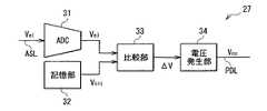
電源電圧調整回路27は、制御信号21Aの入力に応じて(同期して)、調整用画素17に含まれる有機EL素子12の電圧変動に応じた値の電源電圧を発生させるものである。電源電圧調整回路27は、例えば、図6に示したように、ADC(Analog Digital Converter)31と、記憶部32と、比較部33と、電圧発生部34とを有している。ADC31の入力端(図示せず)は、図3、図6に示したように、アノード信号線ASLに接続されており、ADC31の出力端(図示せず)および記憶部32の出力端(図示せず)が比較部33の入力端(図示せず)に接続されている。比較部33の出力端(図示せず)は電圧発生部34の入力端(図示せず)に接続されており、電圧発生部34の出力端(図示せず)が電源電圧伝播線PDLに接続されている。 The power supply
ADC31は、入力されたアナログ信号(アノードの電圧Vel)をデジタル信号に変換するものである。記憶部32は、有機EL素子12の初期電圧Vini(=Vel(0))(基準電圧)を記憶している。比較部33は、ADC31から入力されたデジタル信号(アノードの電圧Vel)と、記憶部32から読み出した初期電圧Viniとを対比することにより、調整用画素17に含まれる有機EL素子12の電圧変動量ΔVを導出するようになっている。具体的には、比較部33は、アノードの電圧Velと初期電圧Viniとの差分を取ることにより、アノードの電圧Velの電圧変動量ΔV(=Vel−Vini)を導出するようになっている。The
電圧発生部34は、電圧変動量ΔVを用いて各表示画素15に印加する電源電圧値を導出し、導出した電源電圧値の電源電圧Vccを、各表示画素15(各電源電圧伝播線PDL)に印加するようになっている。具体的には、電圧発生部34は、電圧変動量ΔVを用いて、駆動トランジスタTr1を飽和領域で駆動させるのに必要な電源電圧値を導出し、導出した電源電圧値の電源電圧Vccを、各表示画素15(各電源電圧伝播線PDL)に印加するようになっている。電源電圧Vccの値は、駆動トランジスタTr1を飽和領域で駆動させるのに必要な最低限の電圧値であることが好ましい。つまり、電圧発生部34は、ADC31でモニターされた発光時の電圧値の変動に応じた値の電源電圧を各表示画素15に印加するようになっている。
ここで、飽和領域とは、例えば、図7に示したように、有機EL素子11に流れる電流Idsが駆動トランジスタTr1のドレイン−ソース間電圧Vdsの値に依らず一定となっている領域を指している。なお、飽和領域において、電流Idsが駆動トランジスタTr1のドレイン−ソース間電圧Vdsの値に依らず完全に一定となっている必要はない。飽和領域は、電流Idsが駆動トランジスタTr1のドレイン−ソース間電圧Vdsの値に依って大きく変動する線形領域と比べて電流Idsの変化率が緩やかな領域も含んでいる。Here, the saturation region is, for example, as shown in FIG. 7, the current Ids flowing through the
(表示装置1の動作)
次に、本実施の形態の表示装置1の動作の一例について説明する。まず、表示装置1に対して外部から映像信号20Aおよび同期信号20Bが入力される。すると、タイミング生成回路21から駆動回路20内の各回路に対して制御信号21Aが出力され、その制御信号21Aの指示に従って、駆動回路20内の各回路が動作する。具体的には、映像信号処理回路22において映像信号22Aが生成され、生成された映像信号22Aが信号線駆動回路23によって各信号線DTLに出力されると同時に、書込線駆動回路24によって複数の書込線WSLの中から一の書込線WSLが順次選択される。さらに、調整用画素駆動回路26において定電流が電流信号線CSLに出力され、出力された定電流が調整用画素17に含まれる有機EL素子12に流れる。有機EL素子12の電圧変動に応じた値の電源電圧が電源電圧調整回路27から電源電圧伝播線PDLに出力され、電源電圧伝播線PDLに出力された電源電圧が電源線駆動回路25によって複数の電源線PSLに順次印加される。これにより、各表示画素15および調整用画素17が駆動され、表示領域10Aに映像が表示される。(Operation of display device 1)
Next, an example of operation | movement of the
(表示装置1の効果)
次に、本実施の形態の表示装置1の効果について説明する。図7に示したように、飽和領域の下端は、階調ごとに異なっており、階調が低くなる程、飽和領域の下端が、駆動トランジスタTr1のドレイン−ソース間電圧Vdsが小さくなる方へ変位する。そのため、有機EL素子11の初期のI−V特性が図中の曲線Aとなっていたとすると、階調が高くなる程、動作点(黒丸)が飽和領域の下端に近づく傾向となっており、階調が高くなる程、動作点(黒丸)と飽和領域の下端とのマージンが小さくなる傾向となっている。従って、有機EL素子11のI−V特性が変位したときに、変位した後のI−V特性が図中の曲線Bとなったとすると、中間階調や低階調においては動作点がまだ飽和領域に入っているが、高階調において動作点が線形領域に入る。(Effect of display device 1)
Next, effects of the
このとき、仮に、全ての階調において動作点が線形領域に入るように、電源電圧Vccの値が予測に基づいて(余裕をもって)設定されたとする。このとき、各表示画素15に印加される映像信号22A(1フィールドの映像信号)に高階調に対応する値が含まれている場合(例えば、図8(A)参照)であっても、余裕をもって、全ての表示画素15において駆動トランジスタTr1を飽和領域で駆動させることが可能となる。しかし、この場合には、電源電圧Vccが、駆動トランジスタTr1を常に飽和領域で駆動させるのに必要な最低限の電源電圧よりも大きくなってしまう。特に、中間階調や低階調においては、設定した電源電圧Vccと、駆動トランジスタTr1を常に飽和領域で駆動させるのに必要な最低限の電源電圧との差が大きくなってしまう。従って、余分に見積もった電圧の分だけ消費電力が高くなってしまう。At this time, it is assumed that the value of the power supply voltageVcc is set based on the prediction (with a margin) so that the operating point falls in the linear region in all gradations. At this time, even when the
一方、本実施の形態では、各表示画素15に含まれる駆動トランジスタTr1において、動作点が常に飽和領域内となるのに必要な電源電圧Vccの値(または、動作点が常に飽和領域内となるのに必要な最低限の電源電圧Vccの値)が設定される。例えば、白輝度(最高階調)に対応する映像信号が一の表示画素15に印加されたときに、その表示画素15内の駆動トランジスタTr1において、動作点が飽和領域の下端(Vds=Vgs−Vth)となるように電源電圧Vccの値が設定される。例えば、初期に設定した電源電圧Vcc(0)(=Vel(0)+Vds(0))に対して、有機EL素子12を白輝度(最高階調)で発光させるのに必要な大きさの定電流が有機EL素子12に印加されているときに得られた電圧変動量ΔVを加えた値(Vcc(0)+ΔV)が、最新の電源電圧Vccの値として設定される。なお、Vel(0)は、有機EL素子11の初期の電圧Velであり、Vds(0)は、駆動トランジスタTr1の初期のドレイン−ソース間電圧Vdsである。On the other hand, in the present embodiment, in the drive transistor Tr1 included in each
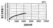
例えば、図9に示したように、初期において、有機EL素子11のアノードの電圧Vel(=Vel(0))が6V、駆動トランジスタTr1のドレイン−ソース間電圧Vds(=Vds(0))が3V、電源電圧Vcc (=Vcc(0))が9Vとなっていたとする。その後、有機EL素子11のI−V特性が変化し、有機EL素子11のアノードの電圧Velが7Vになったとする。このとき、本実施の形態では、例えば、ΔVが単なる予測値(例えば、2V)に設定されず、白輝度(最高階調)に対応する映像信号が一の表示画素15に印加されたときに、その表示画素15内の駆動トランジスタTr1において、動作点が飽和領域の下端となるように設定される。例えば、有機EL素子12を白輝度(最高階調)で発光させるのに必要な大きさの定電流が有機EL素子12に印加されているときに得られた電圧変動量ΔVの値(例えば、1V)がΔVの値として設定される。その後、ΔVがVcc(0)に加えられ、10Vが新たな電源電圧Vcc の値に設定される。このように、本実施の形態では、電源電圧のマージンが予測に基づいて設定された場合と比べて、電源電圧Vccの値を小さくすることができる。従って、消費電力を低く抑えることができる。For example, as shown in FIG. 9, in the initial stage, the anode voltage Vel (= Vel (0)) of the
ところで、図7に示したように、有機EL素子11のI−V特性が変位したときに、変位した後のI−V特性が図中の曲線Bとなるのは、例えば、パネル温度が低くなったとき(図10参照)や、有機EL素子11の通電時間が長くなったとき(図11参照)である。従って、本実施の形態の駆動方法は、パネル温度が低くなったときや、有機EL素子11の通電時間が長くなったときに、特に有効である。 By the way, as shown in FIG. 7, when the IV characteristic of the
<第1の実施の形態の変形例>
上記実施の形態において、調整用画素駆動回路26は、有機EL素子12の発光期間が複数の表示画素15のうちの一の表示画素15(指定画素)に含まれる有機EL素子11の発光期間と同一となるように有機EL素子12に定電流を断続的に印加するようになっていてもよい。例えば、図12に示したように、調整用画素17が第2発光素子に直列に接続されたトランジスタTr5(スイッチング素子)を有しており、タイミング生成回路21が、有機EL素子12の発光期間が指定画素である表示画素15に含まれる有機EL素子11の発光期間と同一となるようにトランジスタTr5をオンオフさせるようになっていてもよい。なお、トランジスタTr5をオンオフ駆動する制御信号は、トランジスタTr5のゲートに接続された制御線CNL2を介して入力される。<Modification of the first embodiment>
In the above embodiment, the adjustment
<第2の実施の形態>
(表示装置2の概略構成)
図13は、本発明の第2の実施の形態に係る表示装置2の概略構成を表したものである。この表示装置2は、調整用画素駆動回路26をなくし、調整用画素17に信号線DTLおよび電源線PSLを接続すると共に、調整用画素17内に画素回路16を設けた点で、上記実施の形態の表示装置1の構成と主に相違する。そこで、以下では、上記実施の形態との相違点について主に説明し、上記実施の形態との共通する点についての説明を適宜、省略するものとする。<Second Embodiment>
(Schematic configuration of the display device 2)
FIG. 13 shows a schematic configuration of the
(調整用画素17)
図14は、非表示領域10B内の回路構成の一例を表したものである。非表示領域10B内には、1つの画素回路16が有機EL素子12と対となって配置されている。なお、本実施の形態では、一対の有機EL素子12および画素回路16が1つの画素(調整用画素17)を構成している。(Adjustment pixel 17)
FIG. 14 illustrates an example of a circuit configuration in the
画素回路16は、上述の画素回路13と同様の構成となっている。具体的には、画素回路16は、駆動トランジスタTr6、書き込みトランジスタTr7および保持容量Cs2によって構成されたものであり、2Tr1Cの回路構成となっている。駆動トランジスタTr6および書き込みトランジスタTr7は、例えば、nチャネルMOS型のTFTにより形成されている。駆動トランジスタTr6または書き込みトランジスタTr7は、例えば、pチャネルMOS型のTFTであってもよい。The
非表示領域10Bにおいて、列方向には信号線DTLが1つ配置され、行方向には書込線WSLおよび電源線PSLがそれぞれ1つずつ配置されている。信号線DTLと書込線WSLとの交差点近傍には、有機EL素子12が設けられている。信号線DTLは、信号線駆動回路23の出力端(図示せず)と、書き込みトランジスタTr7のドレイン電極(図示せず)に接続されている。書込線WSLは、書込線駆動回路24の出力端(図示せず)と、書き込みトランジスタTr7のゲート電極(図示せず)に接続されている。複数の書込線WSLのうち調整用画素17に接続された書込線WSLは、例えば、表示画素15には接続されていない。各電源線PSLは、電源線駆動回路25の出力端(図示せず)と、駆動トランジスタTr6のドレイン電極(図示せず)に接続されている。複数の電源線PSLのうち調整用画素17に接続された電源線PSLは、例えば、表示画素15には接続されていない。書き込みトランジスタTr7のソース電極(図示せず)は、駆動トランジスタTr6のゲート電極(図示せず)と、保持容量Cs2の一端に接続されている。駆動トランジスタTr6のソース電極(図示せず)と保持容量Cs2の他端とが、有機EL素子12のアノード電極(図示せず)に接続されている。有機EL素子12のカソード電極(図示せず)は、例えば、グラウンド線GNDに接続されている。有機EL素子12のアノード電極に、アノード信号線ASLの一端が接続されている。アノード信号線ASLの他端は、電源電圧調整回路27に接続されている。In the
タイミング生成回路21は、例えば、有機EL素子12の発光期間が指定画素である表示画素15に含まれる有機EL素子11の発光期間と同一となるように、指定画素および調整用画素17において、書き込みトランジスタTr2,Tr7を同一のタイミングでオンオフさせると共に駆動トランジスタTr1,Tr6を同一のタイミングでオンオフさせるようになっている。タイミング生成回路21は、例えば、指定画素および調整用画素17において、書き込みトランジスタTr2,Tr7に同一の制御パルスを印加すると共に駆動トランジスタTr1,Tr6に同一の制御パルスを印加するようになっていてもよい。For example, the
信号線駆動回路23は、調整用画素17に対応する信号線DTLに対しては、一定の電圧値の映像信号22A(固定信号)を出力するようになっている。例えば、信号線駆動回路23は、調整用画素17に対応する信号線DTLに対して、白輝度(最高階調)に対応する映像信号22A(固定信号)を出力するようになっている。 The signal
ところで、本実施の形態でも、白輝度(最高階調)に対応する映像信号が一の表示画素15に印加されたときに、その表示画素15内の駆動トランジスタTr1において、動作点が飽和領域の下端となるように電源電圧Vccの値が設定される。すなわち、初期に設定した電源電圧Vcc(0)(=Vel(0)+Vds(0))に対して、有機EL素子12を白輝度(最高階調)で発光させるのに必要な大きさの定電流が有機EL素子12に印加されているときに得られた電圧変動量ΔVを加えた値(Vcc(0)+ΔV)が、最新の電源電圧Vccの値として設定される。これにより、電源電圧のマージンを予測に基づいて設定した場合と比べて、電源電圧Vccの値を小さくすることができる。従って、消費電力を低く抑えることができる。また、本実施の形態の駆動方法も、パネル温度が低くなったときや、有機EL素子11の通電時間が長くなったときに、特に有効である。Incidentally, in this embodiment, when a video signal corresponding to the white luminance (highest gray level) is applied to one
<第2の実施の形態の変形例>
上記第2の実施の形態では、複数の書込線WSLのうち調整用画素17に接続された書込線WSLおよび電源線PSLが表示画素15に接続されていない場合が例示されていたが、表示画素15に接続されていてもよい。例えば、図15に示したように、複数の書込線WSLのうち一番最後の書込線WSL(n)および複数の電源線PSLのうち一番最後の電源線PSL(n)が、表示画素15と、調整用画素17とに接続されていてもよい。<Modification of Second Embodiment>
In the second embodiment, the case where the write line WSL connected to the
また、上記第2の実施の形態では、複数の電源線PSLが互いに電気的に分離して設けられており、電源線駆動回路25によって複数の電源線PSLが順次走査されている場合が例示されていたが、全ての電源線PSLに対して固定電圧が印加されるようになっていてもよい。この場合には、電源電圧調整回路27の出力端が直接、各電源線PSLに接続されていてもよい。ただし、その場合には、電源線駆動回路25の出力端を各電源線PSLから切り離し、画素回路13,16の内部構成を上で例示したものと異ならせてもよい。例えば、図16,図17に示したように、画素回路13,16が、容量素子Cs1(Cs2)と有機EL素子11(12)との接続点と、グラウンド線GNDとの間に、初期化用のトランジスタTr8,Tr9を備えた3Tr1Cの回路構成となっていてもよい。このとき、トランジスタTr8,Tr9のゲートには、例えば、電源線PSL2を介して電源線駆動回路25の出力端が接続されていてもよい。In the second embodiment, a plurality of power supply lines PSL are electrically separated from each other, and the power supply
<第1および第2の実施の形態に共通する変形例>
上記各実施の形態では、調整用画素17は1つだけ設けられていたが、複数設けられていてもよい。また、調整用画素17は非表示領域10Bに設けられていたが、表示領域10A内に設けられていてもよい。<Modifications common to the first and second embodiments>
In each of the above embodiments, only one
また、上記各実施の形態では、電源電圧Vccが調整されていたが、有機EL素子11のカソード電圧が調整されてもよい。In each of the above embodiments, the power supply voltageVcc is adjusted. However, the cathode voltage of the
<適用例>
以下、上記各実施の形態およびそれらの変形例で説明した表示装置1,2の適用例について説明する。上記実施の形態等の表示装置1,2は、テレビジョン装置、デジタルカメラ、ノート型パーソナルコンピュータ、携帯電話等の携帯端末装置あるいはビデオカメラなど、外部から入力された映像信号あるいは内部で生成した映像信号を、画像あるいは映像として表示するあらゆる分野の電子機器の表示装置に適用することが可能である。<Application example>
Hereinafter, application examples of the
(適用例1)
図18は、上記実施の形態等の表示装置1,2が適用されるテレビジョン装置の外観を表したものである。このテレビジョン装置は、例えば、フロントパネル310およびフィルターガラス320を含む映像表示画面部300を有しており、この映像表示画面部300は、上記実施の形態等の表示装置1,2により構成されている。(Application example 1)
FIG. 18 illustrates an appearance of a television device to which the
(適用例2)
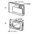
図19は、上記実施の形態等の表示装置1,2が適用されるデジタルカメラの外観を表したものである。このデジタルカメラは、例えば、フラッシュ用の発光部410、表示部420、メニュースイッチ430およびシャッターボタン440を有しており、その表示部420は、上記実施の形態等の表示装置1,2により構成されている。(Application example 2)
FIG. 19 illustrates an appearance of a digital camera to which the
(適用例3)
図20は、上記実施の形態等の表示装置1,2が適用されるノート型パーソナルコンピュータの外観を表したものである。このノート型パーソナルコンピュータは、例えば、本体510,文字等の入力操作のためのキーボード520および画像を表示する表示部530を有しており、その表示部530は、上記実施の形態等の表示装置1,2により構成されている。(Application example 3)
FIG. 20 illustrates an appearance of a notebook personal computer to which the
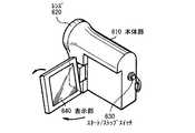
(適用例4)
図21は、上記実施の形態等の表示装置1,2が適用されるビデオカメラの外観を表したものである。このビデオカメラは、例えば、本体部610,この本体部610の前方側面に設けられた被写体撮影用のレンズ620,撮影時のスタート/ストップスイッチ630および表示部640を有しており、その表示部640は、上記実施の形態等の表示装置1,2により構成されている。(Application example 4)
FIG. 21 illustrates an appearance of a video camera to which the
(適用例5)
図22は、上記実施の形態等の表示装置1,2が適用される携帯電話機の外観を表したものである。この携帯電話機は、例えば、上側筐体710と下側筐体720とを連結部(ヒンジ部)730で連結したものであり、ディスプレイ740,サブディスプレイ750,ピクチャーライト760およびカメラ770を有している。そのディスプレイ740またはサブディスプレイ750は、上記実施の形態等の表示装置1,2により構成されている。(Application example 5)
FIG. 22 shows an appearance of a mobile phone to which the
1,2…表示装置、10…表示パネル、10A…表示領域、10B…非表示領域、11,11R,11G,11B,12,12R,12G,12B…有機EL素子、13,16…画素回路、14,14R,14G,14B…サブピクセル、15…表示画素、17…調整用画素、20…駆動回路、20A,22A…映像信号、20B…同期信号、21…タイミング生成回路、21A…制御信号、22…映像信号処理回路、23…信号線駆動回路、24…書込線駆動回路、25…電源線駆動回路、26…調整用画素駆動回路、27…電源電圧調整回路、30…駆動パネル、31…ADC、32…記憶部、33…比較部、34…電圧発生部、40…封止パネル、51…映像信号供給TAB、52…走査信号供給TAB、53…電源電圧供給TAB、54…信号入出力TCP、300…映像表示画面部、310…フロントパネル、320…フィルターガラス、410…発光部、420,530,640…表示部、430…メニュースイッチ、440…シャッターボタン、510…本体、520…キーボード、610…本体部、620…レンズ、630…スタート/ストップスイッチ、710…上側筐体、720…下側筐体、730…連結部、740…ディスプレイ、750…サブディスプレイ、760…ピクチャーライト、770…カメラ、A,B…曲線、ASL…アノード信号線、Cs1,Cs2…保持容量、CNL1,CNL2…制御線、CSL…電流信号線、DTL…信号線、GND…グラウンド線、Ids…電流、PDL…電源電圧伝播線、PSL,PSL(n)…電源線、Tr1,Tr6…駆動トランジスタ、Tr2,Tr5,Tr7…書き込みトランジスタ、Tr3,Tr4…トランジスタ、Vcc,Vcc(0)…電源電圧、Vds,Vds(0)…ドレイン−ソース間電圧、Vel,Vel(0)…電圧、Vini…初期電圧、WSL,WSL(n)…書込線、ΔV…電圧変動量。DESCRIPTION OF
Claims (10)
Translated fromJapanese映像信号に基づいて各表示画素を駆動すると共に、前記第2発光素子に定電流を印加する駆動部と
を備え、
前記駆動部は、前記第2発光素子の電圧変動に応じた値の電源電圧を各表示画素に印加する
表示装置。A display unit having a display area in which a plurality of display pixels including a first light emitting element are two-dimensionally arranged, and a non-display area in which one or a plurality of adjustment pixels including a second light emitting element are disposed;
Driving each display pixel based on a video signal, and applying a constant current to the second light emitting element,
The drive unit applies a power supply voltage having a value corresponding to a voltage variation of the second light emitting element to each display pixel.
請求項1に記載の表示装置。The driving unit derives a voltage fluctuation amount of the second light emitting element by comparing the voltage of the second light emitting element with a reference voltage, and sets a power supply voltage having a value corresponding to the voltage fluctuation amount to each of the power supply voltages. The display device according to claim 1, wherein the display device is applied to a display pixel.
請求項2に記載の表示装置。The display device according to claim 2, wherein the driving unit applies a constant current having a magnitude such that the second light emitting element emits light with white luminance to the second light emitting element.
請求項1ないし請求項3のいずれか一項に記載の表示装置。The drive unit may emit the second light emitting element such that the light emitting period of the second light emitting element is the same as the light emitting period of the first light emitting element included in the designated pixel that is one display pixel of the plurality of display pixels. The display device according to any one of claims 1 to 3, wherein a constant current is intermittently applied to the element.
前記駆動部は、前記第2発光素子の発光期間が前記指定画素に含まれる第1発光素子の発光期間と同一となるように前記スイッチング素子をオンオフさせる
請求項4に記載の表示装置。Each adjustment pixel has a switching element connected in series to the second light emitting element,
The display device according to claim 4, wherein the driving unit turns on and off the switching element so that a light emission period of the second light emitting element is the same as a light emission period of the first light emitting element included in the designated pixel.
各調整用画素は、前記第2発光素子に流れる電流を制御する第3トランジスタと、固定信号に応じた信号電圧を前記第3トランジスタのゲートに書き込む第4トランジスタとを有し、
前記駆動部は、前記第2発光素子の発光期間が前記指定画素に含まれる第1発光素子の発光期間と同一となるように、前記指定画素および各調整用画素において、前記第1トランジスタおよび前記第3トランジスタを同一のタイミングでオンオフさせると共に前記第2トランジスタおよび前記第4トランジスタを同一のタイミングでオンオフさせる
請求項4に記載の表示装置。Each display pixel includes a first transistor that controls a current flowing through the first light emitting element, and a second transistor that writes a signal voltage corresponding to the video signal to the gate of the first transistor,
Each adjustment pixel includes a third transistor that controls a current flowing through the second light emitting element, and a fourth transistor that writes a signal voltage corresponding to a fixed signal to the gate of the third transistor,
The drive unit includes the first transistor and the adjustment pixel in the designated pixel and each adjustment pixel so that a light emission period of the second light emitting element is the same as a light emission period of the first light emitting element included in the designated pixel. The display device according to claim 4, wherein the third transistor is turned on / off at the same timing and the second transistor and the fourth transistor are turned on / off at the same timing.
請求項6に記載の表示装置。The drive unit applies the same first control pulse to the first transistor and the third transistor in the designated pixel and each adjustment pixel, and the same second control to the second transistor and the fourth transistor. The display device according to claim 6, wherein a pulse is applied.
前記第1トランジスタのソースおよびドレインのいずれか一方は前記第1発光素子に接続され、
前記第1トランジスタのソースおよびドレインのうち前記第1発光素子に非接続の方は前記電源電圧が供給される部材に接続されている
請求項1に記載の表示装置。Each display pixel includes a first transistor that controls a current flowing through the first light emitting element, and a second transistor that writes a signal voltage corresponding to the video signal to the gate of the first transistor,
One of the source and the drain of the first transistor is connected to the first light emitting element,
The display device according to claim 1, wherein one of the source and drain of the first transistor that is not connected to the first light emitting element is connected to a member to which the power supply voltage is supplied.
表示装置の駆動方法。A display unit having a display area in which a plurality of display pixels including the first light emitting element are two-dimensionally arranged, and a non-display area in which one or a plurality of adjustment pixels including the second light emitting element are disposed; And a driving unit that applies a constant current to the second light emitting element and supplies a power supply voltage having a value corresponding to a voltage variation of the second light emitting element to each display pixel. A display device driving method including an applying step.
前記表示装置は、
第1発光素子を含む複数の表示画素が2次元配置された表示領域と、第2発光素子を含む1または複数の調整用画素が配置された非表示領域とを有する表示部と、
映像信号に基づいて各表示画素を駆動すると共に、前記第2発光素子に定電流を印加する駆動部と
を有し、
前記駆動部は、前記第2発光素子の電圧変動に応じた値の電源電圧を各表示画素に印加する
電子機器。A display device,
The display device
A display unit having a display area in which a plurality of display pixels including a first light emitting element are two-dimensionally arranged, and a non-display area in which one or a plurality of adjustment pixels including a second light emitting element are disposed;
Driving each display pixel based on a video signal, and applying a constant current to the second light emitting element,
The electronic device, wherein the driving unit applies a power supply voltage having a value corresponding to a voltage variation of the second light emitting element to each display pixel.
Priority Applications (3)
| Application Number | Priority Date | Filing Date | Title |
|---|---|---|---|
| JP2009277813AJP2011118300A (en) | 2009-12-07 | 2009-12-07 | Display device, driving method of the same, and electronic equipment |
| US12/926,206US20110134340A1 (en) | 2009-12-07 | 2010-11-02 | Display device, method of driving the display device, and electronic device |
| CN201010568403.8ACN102087830B (en) | 2009-12-07 | 2010-12-01 | Display device, method of driving the display device, and electronic device |
Applications Claiming Priority (1)
| Application Number | Priority Date | Filing Date | Title |
|---|---|---|---|
| JP2009277813AJP2011118300A (en) | 2009-12-07 | 2009-12-07 | Display device, driving method of the same, and electronic equipment |
Publications (1)
| Publication Number | Publication Date |
|---|---|
| JP2011118300Atrue JP2011118300A (en) | 2011-06-16 |
Family
ID=44081691
Family Applications (1)
| Application Number | Title | Priority Date | Filing Date |
|---|---|---|---|
| JP2009277813APendingJP2011118300A (en) | 2009-12-07 | 2009-12-07 | Display device, driving method of the same, and electronic equipment |
Country Status (3)
| Country | Link |
|---|---|
| US (1) | US20110134340A1 (en) |
| JP (1) | JP2011118300A (en) |
| CN (1) | CN102087830B (en) |
Cited By (3)
| Publication number | Priority date | Publication date | Assignee | Title |
|---|---|---|---|---|
| CN103559860A (en)* | 2013-08-16 | 2014-02-05 | 京东方科技集团股份有限公司 | Pixel circuit driving voltage adjusting method, pixel circuit driving voltage adjusting device, and display apparatus |
| JP2016225109A (en)* | 2015-05-29 | 2016-12-28 | 京セラディスプレイ株式会社 | Light-emitting device |
| US9620057B2 (en) | 2013-08-16 | 2017-04-11 | Boe Technology Group Co., Ltd. | Method and apparatus for adjusting driving voltage for pixel circuit, and display device |
Families Citing this family (6)
| Publication number | Priority date | Publication date | Assignee | Title |
|---|---|---|---|---|
| CN103631547A (en)* | 2012-08-21 | 2014-03-12 | 中国移动通信集团公司 | Display method and device for mobile terminal screen |
| WO2015059593A1 (en)* | 2013-10-21 | 2015-04-30 | Ignis Innovation Inc. | System and methods for power conservation for amoled pixel drivers |
| KR102544322B1 (en)* | 2016-09-26 | 2023-06-19 | 삼성디스플레이 주식회사 | Light emitting display device |
| WO2018102996A1 (en)* | 2016-12-06 | 2018-06-14 | 华为技术有限公司 | Display panel, display apparatus and method for controlling display panel |
| CN110021263B (en)* | 2018-07-05 | 2020-12-22 | 京东方科技集团股份有限公司 | Pixel circuit and driving method thereof, and display panel |
| CN111369946A (en)* | 2018-12-25 | 2020-07-03 | 华为终端有限公司 | Display screen, mobile terminal and control method thereof |
Citations (9)
| Publication number | Priority date | Publication date | Assignee | Title |
|---|---|---|---|---|
| JP2006011410A (en)* | 2004-05-21 | 2006-01-12 | Semiconductor Energy Lab Co Ltd | Display device and electronic apparatus using the same |
| JP2006047578A (en)* | 2004-08-03 | 2006-02-16 | Tohoku Pioneer Corp | Driving device for light emitting display panel |
| JP2006048011A (en)* | 2004-06-29 | 2006-02-16 | Semiconductor Energy Lab Co Ltd | Display device, its driving method, and electronic equipment |
| JP2006047984A (en)* | 2004-05-21 | 2006-02-16 | Semiconductor Energy Lab Co Ltd | Display device and electronic equipment using the same |
| JP2006071686A (en)* | 2004-08-31 | 2006-03-16 | Tohoku Pioneer Corp | Device for driving light-emitting display panel |
| JP2007140489A (en)* | 2005-10-18 | 2007-06-07 | Semiconductor Energy Lab Co Ltd | Display device and electronic apparatus provided with this display device |
| JP2009025741A (en)* | 2007-07-23 | 2009-02-05 | Hitachi Displays Ltd | Image display apparatus and pixel deterioration correction method thereof |
| JP2009075320A (en)* | 2007-09-20 | 2009-04-09 | Sony Corp | Display device and display driving method |
| JP2009192854A (en)* | 2008-02-15 | 2009-08-27 | Casio Comput Co Ltd | Display drive device, display device and drive control method thereof |
Family Cites Families (8)
| Publication number | Priority date | Publication date | Assignee | Title |
|---|---|---|---|---|
| JP4092857B2 (en)* | 1999-06-17 | 2008-05-28 | ソニー株式会社 | Image display device |
| JP3991003B2 (en)* | 2003-04-09 | 2007-10-17 | 松下電器産業株式会社 | Display device and source drive circuit |
| US7482629B2 (en)* | 2004-05-21 | 2009-01-27 | Semiconductor Energy Laboratory Co., Ltd. | Display device and electronic device |
| US7442950B2 (en)* | 2004-12-06 | 2008-10-28 | Semiconductor Energy Laboratory Co., Ltd. | Light emitting device |
| JP2008299019A (en)* | 2007-05-30 | 2008-12-11 | Sony Corp | Cathode potential controller, self light emission display device, electronic equipment and cathode potential control method |
| JP2009031711A (en)* | 2007-07-27 | 2009-02-12 | Samsung Sdi Co Ltd | Organic electroluminescent display device and driving method thereof |
| KR20090011702A (en)* | 2007-07-27 | 2009-02-02 | 삼성모바일디스플레이주식회사 | Organic light emitting display |
| KR100907399B1 (en)* | 2007-11-30 | 2009-07-10 | 삼성모바일디스플레이주식회사 | Organic light emitting display device and driving method thereof |
- 2009
- 2009-12-07JPJP2009277813Apatent/JP2011118300A/enactivePending
- 2010
- 2010-11-02USUS12/926,206patent/US20110134340A1/ennot_activeAbandoned
- 2010-12-01CNCN201010568403.8Apatent/CN102087830B/ennot_activeExpired - Fee Related
Patent Citations (9)
| Publication number | Priority date | Publication date | Assignee | Title |
|---|---|---|---|---|
| JP2006011410A (en)* | 2004-05-21 | 2006-01-12 | Semiconductor Energy Lab Co Ltd | Display device and electronic apparatus using the same |
| JP2006047984A (en)* | 2004-05-21 | 2006-02-16 | Semiconductor Energy Lab Co Ltd | Display device and electronic equipment using the same |
| JP2006048011A (en)* | 2004-06-29 | 2006-02-16 | Semiconductor Energy Lab Co Ltd | Display device, its driving method, and electronic equipment |
| JP2006047578A (en)* | 2004-08-03 | 2006-02-16 | Tohoku Pioneer Corp | Driving device for light emitting display panel |
| JP2006071686A (en)* | 2004-08-31 | 2006-03-16 | Tohoku Pioneer Corp | Device for driving light-emitting display panel |
| JP2007140489A (en)* | 2005-10-18 | 2007-06-07 | Semiconductor Energy Lab Co Ltd | Display device and electronic apparatus provided with this display device |
| JP2009025741A (en)* | 2007-07-23 | 2009-02-05 | Hitachi Displays Ltd | Image display apparatus and pixel deterioration correction method thereof |
| JP2009075320A (en)* | 2007-09-20 | 2009-04-09 | Sony Corp | Display device and display driving method |
| JP2009192854A (en)* | 2008-02-15 | 2009-08-27 | Casio Comput Co Ltd | Display drive device, display device and drive control method thereof |
Cited By (4)
| Publication number | Priority date | Publication date | Assignee | Title |
|---|---|---|---|---|
| CN103559860A (en)* | 2013-08-16 | 2014-02-05 | 京东方科技集团股份有限公司 | Pixel circuit driving voltage adjusting method, pixel circuit driving voltage adjusting device, and display apparatus |
| CN103559860B (en)* | 2013-08-16 | 2015-07-22 | 京东方科技集团股份有限公司 | Pixel circuit driving voltage adjusting method, pixel circuit driving voltage adjusting device, and display apparatus |
| US9620057B2 (en) | 2013-08-16 | 2017-04-11 | Boe Technology Group Co., Ltd. | Method and apparatus for adjusting driving voltage for pixel circuit, and display device |
| JP2016225109A (en)* | 2015-05-29 | 2016-12-28 | 京セラディスプレイ株式会社 | Light-emitting device |
Also Published As
| Publication number | Publication date |
|---|---|
| US20110134340A1 (en) | 2011-06-09 |
| CN102087830B (en) | 2015-05-13 |
| CN102087830A (en) | 2011-06-08 |
Similar Documents
| Publication | Publication Date | Title |
|---|---|---|
| JP5804732B2 (en) | Driving method, display device, and electronic apparatus | |
| JP2011118301A (en) | Display device, method for driving the same, and electronic equipment | |
| JP2011118300A (en) | Display device, driving method of the same, and electronic equipment | |
| KR102701054B1 (en) | Driving method for display device and display device drived thereby | |
| JP2011112723A (en) | Display device, method of driving the same and electronic equipment | |
| US8217868B2 (en) | Display device and method of driving the same | |
| KR20110058668A (en) | Display device, driving method thereof, and electronic device | |
| CN102867840A (en) | Pixel circuit, display device, electronic apparatus, and method of driving pixel circuit | |
| JP2011112722A (en) | Display device, method of driving the same and electronic equipment | |
| TW201037662A (en) | Display device, display device drive method, and electronic apparatus | |
| JP2009157019A (en) | Display device and electronic equipment | |
| KR101497538B1 (en) | display device and electronic equipment | |
| CN102376244A (en) | Displaying apparatus | |
| JP2011128442A (en) | Display panel, display device and electronic equipment | |
| JP2010038928A (en) | Display device, method for driving the same, and electronic device | |
| JP2010117475A (en) | Display apparatus, electronic device, and method of driving the display apparatus | |
| JP5577719B2 (en) | Display device, driving method thereof, and electronic apparatus | |
| JP2011022462A (en) | Display device, driving method therefor, and electronics device | |
| KR101992491B1 (en) | Pixel circuit, display panel, display unit, and electronic system | |
| JP5793058B2 (en) | Display panel, display device and electronic device | |
| JP5321304B2 (en) | Display device, driving method thereof, and electronic apparatus | |
| TWI399723B (en) | Display apparatus, driving method for display apparatus and electronic apparatus | |
| JP5282970B2 (en) | Display device, driving method thereof, and electronic apparatus | |
| JP2009098428A (en) | Display device and its driving method, and electronic equipment | |
| JP2008203655A (en) | Image display and its driving method |
Legal Events
| Date | Code | Title | Description |
|---|---|---|---|
| A621 | Written request for application examination | Free format text:JAPANESE INTERMEDIATE CODE: A621 Effective date:20121114 | |
| A131 | Notification of reasons for refusal | Free format text:JAPANESE INTERMEDIATE CODE: A131 Effective date:20130612 | |
| A977 | Report on retrieval | Free format text:JAPANESE INTERMEDIATE CODE: A971007 Effective date:20130612 | |
| A521 | Request for written amendment filed | Free format text:JAPANESE INTERMEDIATE CODE: A523 Effective date:20130802 | |
| A02 | Decision of refusal | Free format text:JAPANESE INTERMEDIATE CODE: A02 Effective date:20130827 |