Movatterモバイル変換


[0]ホーム

URL:


JP2011118179A - Mems optical scanner - Google Patents

Mems optical scanner
Download PDF

Info

Publication number
JP2011118179A
JP2011118179AJP2009275850AJP2009275850AJP2011118179AJP 2011118179 AJP2011118179 AJP 2011118179AJP 2009275850 AJP2009275850 AJP 2009275850AJP 2009275850 AJP2009275850 AJP 2009275850AJP 2011118179 AJP2011118179 AJP 2011118179A
Authority
JP
Japan
Prior art keywords
substrate
optical scanner
diffraction grating
movable
mems optical
Prior art date
Legal status (The legal status is an assumption and is not a legal conclusion. Google has not performed a legal analysis and makes no representation as to the accuracy of the status listed.)
Granted
Application number
JP2009275850A
Other languages
Japanese (ja)
Other versions
JP5351729B2 (en
Inventor
Hiroaki Tachibana
宏明 橘
Kiyohiko Kono
清彦 河野
Yoshiki Hayazaki
嘉城 早崎
Hiroshi Kawada
裕志 河田
Hideki Ueda
英喜 上田
Current Assignee (The listed assignees may be inaccurate. Google has not performed a legal analysis and makes no representation or warranty as to the accuracy of the list.)
Panasonic Electric Works Co Ltd
Original Assignee
Panasonic Electric Works Co Ltd
Priority date (The priority date is an assumption and is not a legal conclusion. Google has not performed a legal analysis and makes no representation as to the accuracy of the date listed.)
Filing date
Publication date
Application filed by Panasonic Electric Works Co LtdfiledCriticalPanasonic Electric Works Co Ltd
Priority to JP2009275850ApriorityCriticalpatent/JP5351729B2/en
Publication of JP2011118179ApublicationCriticalpatent/JP2011118179A/en
Application grantedgrantedCritical
Publication of JP5351729B2publicationCriticalpatent/JP5351729B2/en
Expired - Fee Relatedlegal-statusCriticalCurrent
Anticipated expirationlegal-statusCritical

Links

Images

Landscapes

Abstract

Translated fromJapanese

【課題】光学振れ角を大きくすることが可能で且つ不要な光が出射されるのを防止することが可能なMEMS光スキャナを提供する。
【解決手段】SOI基板(半導体基板)100を用いて形成され、外側フレーム部10、ミラー面21が設けられた可動部20、一対の捩りばね部30,30を有する可動部形成基板1と、第1のガラス基板200を用いて形成され可動部形成基板1の一表面側に接合された第1のカバー基板2とを備える。可動部形成基板1の可動部20のミラー面21側に回折格子5が形成されており、第1のカバー基板2が、入射光および、回折格子5の法線に対して入射光とは反対側にある負の次数の回折光のうち規定次数の回折光以外を遮光するカバー基板を構成している。
【選択図】図1
A MEMS optical scanner capable of increasing an optical deflection angle and preventing unnecessary light from being emitted is provided.
A movable part forming substrate 1 formed by using an SOI substrate (semiconductor substrate) 100, having an outer frame part 10, a movable part 20 provided with a mirror surface 21, and a pair of torsion spring parts 30, 30; And a first cover substrate 2 formed using the first glass substrate 200 and bonded to one surface side of the movable part forming substrate 1. The diffraction grating 5 is formed on the mirror surface 21 side of the movable part 20 of the movable part forming substrate 1. The first cover substrate 2 is opposite to the incident light with respect to the incident light and the normal line of the diffraction grating 5. The cover substrate is configured to shield the negative-order diffracted light other than the specified-order diffracted light on the side.
[Selection] Figure 1

Description

Translated fromJapanese

本発明は、MEMS光スキャナに関するものである。  The present invention relates to a MEMS optical scanner.

近年、マイクロマシニング技術などを利用して形成されるMEMS(micro electro mechanical systems)デバイスの一種として、マイクロマシニング技術などを利用して形成されて、光を反射する可動部と、可動部を駆動する駆動手段とを備え、可動部に入射する光を走査するMEMS光スキャナが各所で研究開発されている(例えば、特許文献1,2参照)。なお、この種のMEMS光スキャナは、例えば、レーザプロジェクタ、レーザビームプリンタ、バーコードリーダ、内視鏡、距離画像センサなどの種々の光学機器への応用が考えられている。  In recent years, as a type of MEMS (micro electro mechanical systems) device formed using micromachining technology, etc., it is formed using micromachining technology and the like, and a movable portion that reflects light and a movable portion are driven. Research and development of MEMS optical scanners that include driving means and scan light incident on a movable part has been made in various places (see, for example,Patent Documents 1 and 2). Note that this type of MEMS optical scanner is considered to be applied to various optical devices such as a laser projector, a laser beam printer, a barcode reader, an endoscope, and a distance image sensor.

ここにおいて、上記特許文献1には、図11に示すように、導電性を有する第1のシリコン層(活性層)100a’と第2のシリコン層(シリコン基板)100b’との間に絶縁層(SiO層)100c’が介在する上述のSOI基板100’を用いて形成され一表面側に金属膜(アルミニウム膜)からなる反射膜21a’が設けられた可動部20’を有する可動部形成基板1’と、可動部形成基板1’の他表面側に接合された支持基板4’とを備えたMEMS光スキャナが提案されている。なお、上記特許文献1には、支持基板4’として、シリコン基板400a’上にシリコン酸化膜400b’が形成されたものを用いることが記載されているが、ガラス基板を用いてもよいことも記載されている。Here, inPatent Document 1, as shown in FIG. 11, an insulating layer is provided between a conductive first silicon layer (active layer) 100a ′ and a second silicon layer (silicon substrate) 100b ′. movable portion formed with a (SiO2 layer) 100c metal filmreflective film 21a made of (aluminum film) 'movable portion 20 is provided' on the one surface side is formed by using the 'aforementioned SOI substrate 100 or intervening' A MEMS optical scanner including asubstrate 1 ′ and asupport substrate 4 ′ bonded to the other surface side of the movablepart forming substrate 1 ′ has been proposed. In addition, in the above-mentionedPatent Document 1, it is described that thesupport substrate 4 ′ is a substrate in which asilicon oxide film 400b ′ is formed on asilicon substrate 400a ′. However, a glass substrate may be used. Are listed.

上述の可動部形成基板1’は、矩形枠状の外側フレーム部10’と、外側フレーム部10’の内側に配置され反射膜21a’が設けられた矩形板状の可動部20’と、外側フレーム部10’の内側で可動部20’を挟む形で配置され外側フレーム部10’と可動部20’とを連結し捩れ変形が可能な一対の捩りばね部30’,30’とを備えている。また、可動部形成基板1’は、可動部20’において一対の捩りばね部30’,30’を結ぶ方向に直交する方向の両側に形成された櫛形状の可動電極22’,22’と、外側フレーム部10’に形成され可動電極22’の複数の可動櫛歯片22b’に対向する複数の固定櫛歯片12b’を有する櫛形状の固定電極12’,12’とで構成され静電力により可動部20’を駆動する静電駆動式の駆動手段を備えている。  The movablepart forming substrate 1 ′ includes a rectangular frame-shapedouter frame part 10 ′, a rectangular plate-shapedmovable part 20 ′ provided on the inner side of theouter frame part 10 ′ and provided with areflective film 21a ′, and an outer side. A pair oftorsion spring portions 30 ′ and 30 ′ that are arranged inside theframe portion 10 ′ so as to sandwich themovable portion 20 ′ and connect theouter frame portion 10 ′ and themovable portion 20 ′ and can be torsionally deformed are provided. Yes. Further, the movableportion forming substrate 1 ′ includes comb-shapedmovable electrodes 22 ′ and 22 ′ formed on both sides in a direction orthogonal to a direction connecting the pair oftorsion spring portions 30 ′ and 30 ′ in themovable portion 20 ′. Composed of comb-shapedfixed electrodes 12 ′ and 12 ′ having a plurality of fixedcomb teeth 12b ′ opposed to the plurality ofmovable comb teeth 22b ′ of themovable electrode 22 ′ formed on theouter frame portion 10 ′. Thus, an electrostatic drive type driving means for driving themovable portion 20 ′ is provided.

ところで、図11に示した構成のMEMS光スキャナでは、可動部形成基板1’の厚み方向(図11(b),(c)の上下方向)における可動櫛歯片22b’の中心位置と固定櫛歯片12b’の中心位置との差を大きくすることで、可動部20’の機械振れ角を大きくすることができる。  By the way, in the MEMS optical scanner having the configuration shown in FIG. 11, the center position of the movablecomb tooth piece 22b ′ and the fixed comb in the thickness direction of the movablepart forming substrate 1 ′ (vertical direction in FIGS. 11B and 11C). By increasing the difference from the center position of thetooth piece 12b ′, the mechanical deflection angle of themovable portion 20 ′ can be increased.

しかしながら、図11に示した構成のMEMS光スキャナでは、得られる光学振れ角は、せいぜい、可動部20’の機械振れ角の2倍程度である。  However, in the MEMS optical scanner having the configuration shown in FIG. 11, the obtained optical deflection angle is at most about twice the mechanical deflection angle of the movable portion 20 '.

これに対して、上記特許文献2には、光学振れ角を大きくできるMEMS光スキャナとして、図12に示すように、シリコン基板110”を用いて形成され一表面側に回折格子5”が設けられた可動部20”を有する可動部形成基板1”と、可動部形成基板1”の他表面側に接合された支持基板4”とを備えた構成のものが提案されている。ここで、可動部形成基板1”は、矩形枠状の外側フレーム部10”と、外側フレーム部10”の内側に配置されミラー面(反射面)21”に回折格子5”が設けられた矩形板状の可動部20”と、外側フレーム部10”の内側で可動部20”を挟む形で配置され外側フレーム部10”と可動部20”とを連結する一対の梁部31”,31”とを備えている。  On the other hand, inPatent Document 2, as a MEMS optical scanner capable of increasing the optical deflection angle, as shown in FIG. 12, asilicon substrate 110 ″ is used and a diffraction grating 5 ″ is provided on one surface side. A structure having a movablepart forming substrate 1 ″ having amovable part 20 ″ and asupport substrate 4 ″ bonded to the other surface side of the movablepart forming substrate 1 ″ has been proposed. Here, the movableportion forming substrate 1 ″ is a rectangular frame-shapedouter frame portion 10 ″ and a rectangular shape in which a diffraction grating 5 ″ is provided on a mirror surface (reflection surface) 21 ″ disposed inside theouter frame portion 10 ″. A plate-shapedmovable portion 20 ″ and a pair ofbeam portions 31 ″, 31 ″ that are arranged to sandwich themovable portion 20 ″ inside theouter frame portion 10 ″ and connect theouter frame portion 10 ″ and themovable portion 20 ″. And.

特開2004−266991号公報JP 2004-266991 A特開2007−272066号公報JP 2007-272066 A

しかしながら、図12に示した構成のMEMS光スキャナでは、回折格子5”での多数の次数(κ=0,±1,±2,・・・)の回折光が外部へ出射されてしまう、つまり、不要な光も出射されてしまうという問題があった。なお、0次(κ=0)の回折光は、反射光である。  However, in the MEMS optical scanner having the configuration shown in FIG. 12, diffracted light of many orders (κ = 0, ± 1, ± 2,...) At the diffraction grating 5 ″ is emitted to the outside. There is a problem that unnecessary light is also emitted, and the 0th-order (κ = 0) diffracted light is reflected light.

本発明は上記事由に鑑みて為されたものであり、その目的は、光学振れ角を大きくすることが可能で且つ不要な光が出射されるのを防止することが可能なMEMS光スキャナを提供することにある。  The present invention has been made in view of the above-mentioned reasons, and an object thereof is to provide a MEMS optical scanner capable of increasing an optical deflection angle and preventing unnecessary light from being emitted. There is to do.

請求項1の発明は、半導体基板を用いて形成され、外側フレーム部、外側フレーム部の内側に配置され一表面側にミラー面が設けられた可動部、および外側フレーム部の内側で可動部を挟む形で配置され外側フレーム部と可動部とを連結し捩れ変形が可能な一対の捩りばね部を有する可動部形成基板と、可動部を駆動する駆動手段とを備えたMEMS光スキャナであって、可動部形成基板の可動部のミラー面側に回折格子が形成されてなり、入射光および、回折格子の法線に対して入射光とは反対側にある負の次数の回折光のうち規定次数の回折光以外を遮光するカバー基板が可動部形成基板に接合されてなることを特徴とする。  The invention ofclaim 1 is formed using a semiconductor substrate, and includes an outer frame part, a movable part disposed inside the outer frame part and provided with a mirror surface on one surface side, and a movable part inside the outer frame part. A MEMS optical scanner provided with a movable part forming substrate having a pair of torsion spring parts that are arranged in a sandwiched manner and connect to an outer frame part and a movable part and capable of torsional deformation, and drive means for driving the movable part. The diffraction grating is formed on the mirror surface side of the movable part of the movable part forming substrate, and the incident light and the negative order diffracted light on the side opposite to the incident light with respect to the normal line of the diffraction grating are defined. A cover substrate that shields light other than the diffracted light of the order is bonded to the movable portion forming substrate.

この発明によれば、可動部形成基板の可動部のミラー面側に回折格子が形成されてなり、入射光および、回折格子の法線に対して入射光とは反対側にある負の次数の回折光のうち規定次数の回折光以外を遮光するカバー基板が可動部形成基板に接合されているので、光学振れ角を大きくすることが可能で且つ不要な光が出射されるのを防止することが可能となる。  According to the present invention, the diffraction grating is formed on the mirror surface side of the movable part of the movable part forming substrate, and the incident light and the negative order on the opposite side to the incident light with respect to the normal line of the diffraction grating. Since the cover substrate that shields the diffracted light other than the diffracted light of the specified order is joined to the movable part forming substrate, the optical deflection angle can be increased and unnecessary light can be prevented from being emitted. Is possible.

請求項2の発明は、請求項1の発明において、前記回折格子は、平面視において格子周期方向に直交する方向を、前記各捩りばね部の並設方向に対して非平行としてあることを特徴とする。  According to a second aspect of the present invention, in the first aspect of the invention, the diffraction grating has a direction orthogonal to the grating periodic direction in plan view that is not parallel to the parallel arrangement direction of the torsion spring portions. And

この発明によれば、前記各捩りばね部の並設方向に直交する平面に沿って前記回折格子に入射光を入射させて用いる場合に、前記回折格子からの0次の回折光を当該平面に沿って進行させて前記カバー基板で遮光する一方で、前記規定次数の回折光を当該平面から傾いた面に沿って進行させ前記カバー基板から出射させることができる。  According to the present invention, when incident light is incident on the diffraction grating along a plane orthogonal to the parallel arrangement direction of the torsion spring portions, zero-order diffracted light from the diffraction grating is applied to the plane. The diffracted light of the specified order can be caused to travel along a plane inclined from the plane and emitted from the cover substrate while being shielded from light by the cover substrate.

請求項3の発明は、請求項1または請求項2の発明において、前記回折格子は、前記可動部における前記ミラー面側に周期的な溝を設けることにより形成されてなることを特徴とする。  According to a third aspect of the present invention, in the first or second aspect of the present invention, the diffraction grating is formed by providing a periodic groove on the mirror surface side of the movable portion.

この発明によれば、高い回折効率を得ることができる。  According to this invention, high diffraction efficiency can be obtained.

請求項4の発明は、請求項1ないし請求項3の発明において、前記回折格子は、溝形状が鋸歯状であることを特徴とする。  According to a fourth aspect of the present invention, in the first to third aspects of the invention, the diffraction grating has a sawtooth shape in the groove shape.

この発明によれば、前記回折格子の回折効率を高めることができる。  According to this invention, the diffraction efficiency of the diffraction grating can be increased.

請求項5の発明は、請求項1ないし請求項3の発明において、前記回折格子は、溝形状が矩形状であることを特徴とする。  According to a fifth aspect of the present invention, in the first to third aspects of the invention, the diffraction grating has a rectangular groove shape.

この発明によれば、請求項4の発明に比べて、前記回折格子を容易に形成することができる。  According to the present invention, the diffraction grating can be easily formed as compared with the invention ofclaim 4.

請求項6の発明は、請求項1の発明において、前記回折格子は、相対的に反射率の高い材料からなるライン状の高反射率膜と相対的に反射率の低い材料からなるライン状の低反射率膜とが前記ミラー面に沿って交互に配列されてなることを特徴とする。  According to a sixth aspect of the present invention, in the first aspect of the invention, the diffraction grating has a line-shaped high reflectivity film made of a material having a relatively high reflectivity and a line-shape made of a material having a relatively low reflectivity. The low reflectivity film is alternately arranged along the mirror surface.

この発明によれば、前記回折格子を容易に形成することができる。  According to this invention, the diffraction grating can be easily formed.

請求項7の発明は、請求項6の発明において、前記低反射率膜がSiO膜からなり、前記高反射率膜が金属膜であることを特徴とする。A seventh aspect of the invention is characterized in that, in the sixth aspect of the invention, the low reflectivity film is made of a SiO2 film, and the high reflectivity film is a metal film.

この発明によれば、前記回折格子を一般的なMEMSプロセスとの整合性の良いプロセスで形成することができる。  According to the present invention, the diffraction grating can be formed by a process having good consistency with a general MEMS process.

請求項8の発明は、請求項1ないし請求項7の発明において、前記規定次数が−1であることを特徴とする。  The invention of claim 8 is characterized in that, in the inventions ofclaims 1 to 7, the specified order is -1.

この発明によれば、−1次の回折光を走査光として出射することとなり、走査光の光学振れ角が大きくなりすぎて前記カバー基板の平面サイズが大きくなって小型化が制限されるのを防止することができるとともに、−2次以上の回折光を走査光として利用する場合に比べて走査光の光強度を高めることができる。  According to the present invention, the −1st order diffracted light is emitted as scanning light, and the optical deflection angle of the scanning light becomes too large, so that the planar size of the cover substrate becomes large and miniaturization is restricted. It is possible to prevent this, and it is possible to increase the light intensity of the scanning light as compared with the case where diffracted light of -2nd order or higher is used as the scanning light.

請求項1の発明では、光学振れ角を大きくすることが可能で且つ不要な光が出射されるのを防止することが可能になるという効果がある。  According to the first aspect of the invention, it is possible to increase the optical deflection angle and to prevent unnecessary light from being emitted.

実施形態のMEMS光スキャナの概略分解斜視図である。It is a general | schematic disassembled perspective view of the MEMS optical scanner of embodiment.同上のMEMS光スキャナを示し、(a)は概略平面図、(b)は(a)のA−A’概略断面図である。The MEMS optical scanner same as the above is shown, (a) is a schematic plan view, and (b) is an A-A 'schematic cross-sectional view of (a).同上のMEMS光スキャナの動作説明図である。It is operation | movement explanatory drawing of a MEMS optical scanner same as the above.同上のMEMS光スキャナの動作説明図である。It is operation | movement explanatory drawing of a MEMS optical scanner same as the above.同上のMEMS光スキャナの動作説明図である。It is operation | movement explanatory drawing of a MEMS optical scanner same as the above.同上のMEMS光スキャナの動作説明図である。It is operation | movement explanatory drawing of a MEMS optical scanner same as the above.同上のMEMS光スキャナの要部概略断面図である。It is a principal part schematic sectional drawing of a MEMS optical scanner same as the above.同上のMEMS光スキャナの製造方法を説明するための主要工程断面図である。It is main process sectional drawing for demonstrating the manufacturing method of a MEMS optical scanner same as the above.同上のMEMS光スキャナの他の構成例の要部概略断面図である。It is a principal part schematic sectional drawing of the other structural example of a MEMS optical scanner same as the above.同上のMEMS光スキャナの別の構成例の要部概略断面図である。It is a principal part schematic sectional drawing of another structural example of a MEMS optical scanner same as the above.従来例のMEMS光スキャナを示し、(a)は概略平面図、(b)は(a)のB−B’概略断面図、(c)は(a)のC−C’概略断面図である。1A and 1B show a conventional MEMS optical scanner, in which FIG. 1A is a schematic plan view, FIG. 1B is a schematic cross-sectional view along line BB ′ in FIG. 1A, and FIG. .他の従来例のMEMS光スキャナを示し、(a)は概略斜視図、(b)は概略分解斜視図である。FIG. 6 shows another conventional MEMS optical scanner, in which (a) is a schematic perspective view and (b) is a schematic exploded perspective view.

以下、本実施形態のMEMS光スキャナについて図1〜図7を参照しながら説明する。  Hereinafter, the MEMS optical scanner of the present embodiment will be described with reference to FIGS.

本実施形態のMEMS光スキャナは、半導体基板であるSOI基板100を用いて形成され、外周形状が矩形状の枠状(ここでは、矩形枠状)の外側フレーム部(固定フレーム部)10、外側フレーム部10の内側に配置され平面視矩形状のミラー面21が設けられた平面視矩形状の可動部20、および外側フレーム部10の内側で可動部20を挟む形で配置され外側フレーム部10と可動部20とを連結し捩れ変形が可能な一対の捩りばね部30,30を有する可動部形成基板(可動部形成基板)1と、第1のガラス基板200を用いて形成され可動部形成基板1においてミラー面21が設けられた一表面側に接合された第1のカバー基板2と、第2のガラス基板300を用いて形成され可動部形成基板1の他表面側に接合された第2のカバー基板3とを備えている。また、本実施形態のMEMS光スキャナは、可動部形成基板1の可動部20のミラー面21側に回折格子5が形成されており、第1のカバー基板2が、後述するように、入射光および、回折格子5の法線(回折格子5の格子面の法線)に対して入射光とは反対側にある負の次数の回折光のうち規定次数の回折光以外を遮光するカバー基板を構成している。  The MEMS optical scanner according to the present embodiment is formed using anSOI substrate 100 which is a semiconductor substrate, and has an outer frame portion (fixed frame portion) 10 having an outer peripheral shape of a rectangular shape (here, a rectangular frame shape) and an outer side. Themovable portion 20 having a rectangular shape in plan view and provided with amirror surface 21 having a rectangular shape in plan view disposed inside theframe portion 10 and theouter frame portion 10 disposed so as to sandwich themovable portion 20 inside theouter frame portion 10. The movable part forming substrate (movable part forming substrate) 1 having a pair oftorsion spring parts 30 and 30 that can be torsionally deformed by connecting themovable part 20 and thefirst glass substrate 200 is formed. Thefirst cover substrate 2 bonded to the one surface side where themirror surface 21 is provided in thesubstrate 1 and thesecond glass substrate 300 is used, and thefirst cover substrate 2 is bonded to the other surface side of the movableportion forming substrate 1. 2 mosquitoes And a oversubstrate 3. Further, in the MEMS optical scanner of the present embodiment, thediffraction grating 5 is formed on themirror surface 21 side of themovable portion 20 of the movableportion forming substrate 1, and thefirst cover substrate 2 receives incident light as described later. A cover substrate that shields light other than the diffracted light of the specified order out of the diffracted light of the negative order on the side opposite to the incident light with respect to the normal line of the diffraction grating 5 (the normal line of the grating surface of the diffraction grating 5). It is composed.

上述の可動部形成基板1および各カバー基板2,3の外周形状は矩形状であり、各カバー基板2,3は可動部形成基板1と同じ外形寸法に形成されている。  The outer peripheral shape of the above-mentioned movablepart forming substrate 1 and eachcover substrate 2, 3 is rectangular, and eachcover substrate 2, 3 is formed to have the same outer dimensions as the movablepart forming substrate 1.

ここにおいて、可動部形成基板1は、導電性を有する第1のシリコン層(活性層)100aと第2のシリコン層(シリコン基板)100bとの間に絶縁層(SiO層)100cが介在する上述のSOI基板100をバルクマイクロマシニング技術などにより加工することによって形成してある。また、第1のカバー基板2は、それぞれパイレックス(登録商標)ガラスなどからなる2枚のガラス板を厚み方向に重ねて接合した第2のガラス基板200を用いて形成してあり、第2のカバー基板3は、パイレックス(登録商標)ガラスなどからなる第2のガラス基板300を加工することにより形成してある。なお、SOI基板100は、第1のシリコン層100aの厚さを30μm、第2のシリコン層100bの厚さを400μmに設定し、第1のガラス基板200および第2のガラス基板300の厚さは、0.5mm〜1.5mm程度の範囲で設定してあるが、これらの数値は一例であり、特に限定するものではない。また、半導体基板たるSOI基板100の一表面である第1のシリコン層10cの表面は(100)面としてある。Here, in the movablepart forming substrate 1, an insulating layer (SiO2 layer) 100c is interposed between a conductive first silicon layer (active layer) 100a and a second silicon layer (silicon substrate) 100b. TheSOI substrate 100 described above is formed by processing using a bulk micromachining technique or the like. Thefirst cover substrate 2 is formed by using asecond glass substrate 200 in which two glass plates each made of Pyrex (registered trademark) glass or the like are stacked in the thickness direction and bonded together. Thecover substrate 3 is formed by processing asecond glass substrate 300 made of Pyrex (registered trademark) glass or the like. Note that in theSOI substrate 100, the thickness of thefirst silicon layer 100a is set to 30 μm, the thickness of thesecond silicon layer 100b is set to 400 μm, and the thicknesses of thefirst glass substrate 200 and thesecond glass substrate 300 are set. Is set in the range of about 0.5 mm to 1.5 mm, but these numerical values are examples and are not particularly limited. The surface of the first silicon layer 10c, which is one surface of theSOI substrate 100 as a semiconductor substrate, is a (100) plane.

可動部形成基板1の外側フレーム部10は、SOI基板100の第1のシリコン層100a、絶縁層100c、第2のシリコン層100bそれぞれを利用して形成してあり、外側フレーム部10のうち第1のシリコン層100aにより形成された部位が第1のカバー基板2の外周部と全周に亘って接合され、外側フレーム部10のうち第2のシリコン層100cにより形成された部位が第2のカバー基板3の外周部と全周に亘って接合されており、上記一表面側において外側フレーム部10に、可動部20を駆動する後述の駆動手段に電気的に接続される2つのパッド13,13が形成されている。各パッド13,13は平面視形状が円形状であり、第1の金属膜(例えば、Al膜など)により構成されている。なお、本実施形態では、各パッド13,13の膜厚を500nmに設定してあるが、この数値は一例であり、特に限定するものではない。  Theouter frame portion 10 of the movableportion forming substrate 1 is formed using each of thefirst silicon layer 100a, the insulatinglayer 100c, and thesecond silicon layer 100b of theSOI substrate 100. The portion formed by thefirst silicon layer 100a is joined to the outer periphery of thefirst cover substrate 2 over the entire periphery, and the portion formed by thesecond silicon layer 100c in theouter frame portion 10 is the second. Twopads 13 which are joined to the outer peripheral portion of thecover substrate 3 over the entire periphery and are electrically connected to theouter frame portion 10 on the one surface side, which will be described later, for driving means for driving themovable portion 20; 13 is formed. Each of thepads 13 and 13 has a circular shape in plan view, and is composed of a first metal film (for example, an Al film). In the present embodiment, the thickness of each of thepads 13 and 13 is set to 500 nm, but this numerical value is an example and is not particularly limited.

また、可動部形成基板1の可動部20および各捩りばね部30,30は、SOI基板100の第1のシリコン層100aを用いて形成されており、外側フレーム部10よりも十分に薄肉となっている。また、可動部20に設けられたミラー面21は、可動部20において第1のシリコン層100aの表面により構成されているが、これに限らず、可動部20において第1のシリコン層100aにより形成された部位の表面に第2の金属膜(例えば、Al膜など)からなる反射膜を形成して、当該反射膜の表面が、ミラー面21を構成するようにしてもよい。なお、反射膜を構成する第2の金属膜の材料は、Alに限らず、走査対象(スキャン対象)の光(入射光)の波長や波長帯に応じて、例えば、Ag、Al−Si、Auなどを採用してもよい。  Further, themovable portion 20 and thetorsion spring portions 30, 30 of the movableportion forming substrate 1 are formed using thefirst silicon layer 100 a of theSOI substrate 100 and are sufficiently thinner than theouter frame portion 10. ing. In addition, themirror surface 21 provided on themovable portion 20 is configured by the surface of thefirst silicon layer 100a in themovable portion 20, but is not limited thereto, and is formed by thefirst silicon layer 100a in themovable portion 20. A reflective film made of a second metal film (for example, an Al film) may be formed on the surface of the formed part, and the surface of the reflective film may constitute themirror surface 21. Note that the material of the second metal film constituting the reflective film is not limited to Al, and may be, for example, Ag, Al-Si, depending on the wavelength or wavelength band of the light (incident light) of the scan target (scan target). Au or the like may be employed.

以下では、図2(a),(b)それぞれの左下に示すように、平面視において一対の捩りばね部30,30の並設方向に直交する方向をx軸方向、一対の捩りばね部30,30の並設方向をy軸方向、x軸方向およびy軸方向に直交する方向をz軸方向とする直交座標を利用して説明する。なお、当該直交座標の原点は、平面視における回折格子5の中心O(図6参照)としている。  In the following, as shown in the lower left of each of FIGS. 2A and 2B, the direction orthogonal to the juxtaposed direction of the pair oftorsion spring portions 30, 30 in plan view is the x-axis direction, and the pair oftorsion spring portions 30. , 30 will be described using orthogonal coordinates in which the parallel direction is the y-axis direction, and the direction orthogonal to the x-axis direction and the y-axis direction is the z-axis direction. The origin of the orthogonal coordinates is the center O (see FIG. 6) of thediffraction grating 5 in plan view.

上述の可動部形成基板1は、一対の捩りばね部30,30がy軸方向に並設されており、可動部20が、外側フレーム部10に対して一対の捩りばね部30,30の回りで変位可能となっている(y軸の軸回りで回動可能となっている)。つまり、一対の捩りばね部30,30は、外側フレーム部10に対して可動部20が揺動自在となるように外側フレーム部10と可動部20とを連結している。言い換えれば、外側フレーム部10の内側に配置される可動部20は、可動部20から相反する2方向へ連続一体に延長された2つの捩りばね部30,30を介して外側フレーム部10に揺動自在に支持されている。ここで、一対の捩りばね部30,30は、両者のy軸に沿った中心線同士を結ぶ直線が、平面視で可動部20の重心を通るように形成されている。なお、各捩りばね部30,30は、厚み寸法(z軸に沿った方向の寸法)を30μm、幅寸法(x軸に沿った方向の寸法)を、5μmに設定してあるが、これらの数値は一例であり、特に限定するものではない。また、可動部20およびミラー面21の平面視形状は、矩形状に限らず、例えば、円形状でもよい。また、外側フレーム部10の内周形状も矩形状に限らず、例えば、円形状でもよい。  In the movablepart forming substrate 1 described above, a pair oftorsion spring parts 30, 30 are arranged in parallel in the y-axis direction, and themovable part 20 rotates around the pair oftorsion spring parts 30, 30 with respect to theouter frame part 10. Can be displaced (can be rotated around the y-axis). That is, the pair oftorsion spring portions 30, 30 connects theouter frame portion 10 and themovable portion 20 so that themovable portion 20 can swing with respect to theouter frame portion 10. In other words, themovable part 20 arranged inside theouter frame part 10 swings to theouter frame part 10 via twotorsion spring parts 30 and 30 that are continuously and integrally extended in two opposite directions from themovable part 20. It is supported freely. Here, the pair oftorsion spring portions 30 and 30 are formed such that a straight line connecting the center lines along the y-axis passes through the center of gravity of themovable portion 20 in plan view. Each of the torsion springs 30 and 30 has a thickness dimension (dimension along the z-axis) set to 30 μm and a width dimension (dimension along the x-axis) set to 5 μm. The numerical value is an example and is not particularly limited. Moreover, the planar view shape of themovable part 20 and themirror surface 21 is not limited to a rectangular shape, and may be, for example, a circular shape. Further, the inner peripheral shape of theouter frame portion 10 is not limited to a rectangular shape, and may be a circular shape, for example.

上述の可動部形成基板1は、可動部20において一対の捩りばね部30,30を結ぶ方向(一対の捩りばね部30,30の並設方向)に直交する方向(つまり、x軸方向)の両側に形成された櫛形状の可動電極22と、外側フレーム部10に形成され可動電極22の複数の可動櫛歯片22bに対向する複数の固定櫛歯片12bを有する櫛形状の固定電極12とで構成され静電力により可動部20を駆動する静電駆動式の駆動手段を備えている。なお、本実施形態では、駆動手段が、静電力により可動部20を駆動するものであるが、静電力によって可動部20を駆動する静電駆動式に限らず、電磁力によって可動部20を駆動する電磁駆動式でもよいし、圧電素子によって可動部20を駆動する圧電駆動式でもよい。  In the movablepart forming substrate 1 described above, themovable part 20 has a direction (that is, the x-axis direction) orthogonal to a direction connecting the pair oftorsion spring parts 30 and 30 (a direction in which the pair oftorsion spring parts 30 and 30 are arranged side by side). Comb-shapedmovable electrode 22 formed on both sides, and comb-shaped fixedelectrode 12 having a plurality of fixed comb-tooth pieces 12b formed onouter frame portion 10 and facing a plurality of movable comb-tooth pieces 22b ofmovable electrode 22; It is comprised by the electrostatic drive type drive means which drives themovable part 20 by electrostatic force. In the present embodiment, the driving means drives themovable portion 20 by electrostatic force, but is not limited to the electrostatic drive type that drives themovable portion 20 by electrostatic force, and drives themovable portion 20 by electromagnetic force. It may be an electromagnetic driving type, or a piezoelectric driving type in which themovable portion 20 is driven by a piezoelectric element.

上述の固定電極12,12は、平面視形状が櫛形状であり、櫛骨部12aが外側フレーム部10のうちy軸に沿った枠片部において第1のシリコン層100aにより形成された部位の一部により構成されており、櫛骨部12aにおける可動部20との対向面(外側フレーム部10におけるy軸に沿った内側面)には、第1のシリコン層100aの一部からなる多数の固定櫛歯片12bが一対の捩りばね部30,30の並設方向に沿って列設されている。一方、可動電極22,22は、可動部20における固定電極12の櫛骨部12a側の櫛骨部22a,22aの側面(可動部20におけるy軸に沿った側面)において、第1のシリコン層100aの一部により構成され固定櫛歯片12bにそれぞれ対向する多数の可動櫛歯片22bが上記並設方向に列設されている。ここで、櫛形状の固定電極12と櫛形状の可動電極22とは、櫛骨部12a,22aが互いに対向し、固定電極12の各固定櫛歯片12bが可動電極22の櫛溝に入り組んでおり、固定櫛歯片12bと可動櫛歯片22bとが、y軸方向において互いに離間しており、固定電極12と可動電極22との間に電圧が印加されることにより、固定電極12と可動電極22との間に互いに引き合う方向に作用する静電力が発生する。なお、y軸方向における固定櫛歯片12bと可動櫛歯片22bとの間の隙間は、例えば、5μm〜20μm程度の範囲で適宜設定すればよい。  The above-describedfixed electrodes 12 and 12 have a comb shape in plan view, and thecomb bone portion 12a is a portion of theouter frame portion 10 formed by thefirst silicon layer 100a in the frame piece portion along the y axis. A part of thecomb bone portion 12a facing the movable portion 20 (the inner side surface along the y-axis in the outer frame portion 10) has a large number of parts of thefirst silicon layer 100a. The fixedcomb teeth 12b are arranged along the direction in which the pair oftorsion spring portions 30 and 30 are arranged side by side. On the other hand, themovable electrodes 22, 22 are the first silicon layer on the side surfaces (side surfaces along the y axis in the movable portion 20) of thecomb bone portions 22 a, 22 a on thecomb bone portion 12 a side of the fixedelectrode 12 in themovable portion 20. A large number ofmovable comb teeth 22b that are constituted by a part of 100a and face the fixedcomb teeth 12b, respectively, are arranged in the above-mentioned parallel direction. Here, in the comb-shaped fixedelectrode 12 and the comb-shapedmovable electrode 22, thecomb bone portions 12 a and 22 a face each other, and the fixedcomb teeth 12 b of the fixedelectrode 12 enter the comb groove of themovable electrode 22. The fixedcomb tooth piece 12b and the movablecomb tooth piece 22b are separated from each other in the y-axis direction, and a voltage is applied between the fixedelectrode 12 and themovable electrode 22, whereby the fixedelectrode 12 and themovable electrode tooth 22b are movable. An electrostatic force acting in a direction attracting each other is generated between theelectrodes 22. In addition, what is necessary is just to set the clearance gap between the fixed comb-tooth piece 12b in the y-axis direction and the movable comb-tooth piece 22b suitably in the range of about 5 micrometers-20 micrometers, for example.

可動部形成基板1の外側フレーム部10において第1のシリコン層100aにより形成された部位には、一方のパッド13(図1における右側のパッド13b)が固定電極12,12に電気的に接続されるとともに他方のパッド13(図1における左側のパッド13a)が可動電極22,22に電気的に接続され、且つ、固定電極12,12と可動電極22,22とが電気的に絶縁されるように、複数のスリット10a,10a,10aが絶縁層100cに達する深さで形成されている。ここで、本実施形態では、各スリット10a,10a,10aをトレンチとし、各スリット10a,10a,10aの平面視形状を外側フレーム部10の外側面側に開放されない形状とすることで、外側フレーム部10にスリット10a,10a,10aを形成した構造を採用しながらも、外側フレーム部10と第1のカバー基板2との接合性が低下するのを防止し、外側フレーム部10と各カバー基板2,3とで囲まれる空間の気密性を確保している。  One pad 13 (the right pad 13b in FIG. 1) is electrically connected to the fixedelectrodes 12 and 12 at a portion formed by thefirst silicon layer 100a in theouter frame portion 10 of the movableportion forming substrate 1. And the other pad 13 (leftpad 13a in FIG. 1) is electrically connected to themovable electrodes 22 and 22, and the fixedelectrodes 12 and 12 and themovable electrodes 22 and 22 are electrically insulated. In addition, a plurality ofslits 10a, 10a, 10a are formed to a depth reaching the insulatinglayer 100c. Here, in this embodiment, eachslit 10a, 10a, 10a is made into a trench, and the plan view shape of eachslit 10a, 10a, 10a is made into the shape which is not open | released by the outer surface side of the outerside frame part 10, By this While adopting the structure in which theslits 10a, 10a, 10a are formed in theportion 10, it is possible to prevent the bonding property between theouter frame portion 10 and thefirst cover substrate 2 from being lowered, and theouter frame portion 10 and each cover substrate. The airtightness of the space surrounded by 2 and 3 is secured.

ここで、外側フレーム部10において第1のシリコン層100aにより形成された部分は、上述のスリット10a,10a,10aを形成することにより、一端部が可動部20の外側面に連続一体に連結された各捩りばね部30,30それぞれの他端部が内側面に連続一体に連結された2つのアンカー部11a,11bと、一方のアンカー部11aaと一方のパッド13aが形成された矩形状の島部11cと、上記一方のアンカー部11abと島部11acとをつなぐ平面視L字状の導電部11adとで構成される第1の導電性構造体11aが、可動部20の可動電極22,22と同電位になり、残りの部分からなり他方のパッド13bが形成された第2の導電性構造体11bが固定電極12,12と同電位になる。  Here, the portion formed by thefirst silicon layer 100a in theouter frame portion 10 is connected to the outer surface of themovable portion 20 in an integrated manner by forming theslits 10a, 10a, 10a described above. In addition, the torsion springs 30 and 30 have a rectangular island formed with twoanchor portions 11a and 11b in which the other end portions of thetorsion spring portions 30 and 30 are continuously and integrally connected to the inner surface, and one anchor portion 11aa and onepad 13a. The firstconductive structure 11a composed of the part 11c and the L-shaped conductive part 11ad in plan view connecting the one anchor part 11ab and the island part 11ac is themovable electrodes 22, 22 of themovable part 20. And the secondconductive structure 11b formed of the remaining portion and having the other pad 13b formed is at the same potential as the fixedelectrodes 12 and 12.

第1のカバー基板2は、上述のように第1のガラス基板200を用いており、第1のガラス基板200の厚み方向に貫通して各パッド13,13それぞれを全周に亘って露出させる2つの貫通孔202,202が形成されている。ここにおいて、第1のガラス基板200の各貫通孔202,202は、可動部形成基板1から離れるにつれて開口面積が徐々に大きくなるテーパ状に形成されている。ここで、第1のカバー基板2の各貫通孔202,202は、サンドブラスト法により形成してあるが、サンドブラスト法に限定するものではなく、貫通孔202,202の形状によってはドリル加工法やエッチング法などを適宜採用してもよい。  As described above, thefirst cover substrate 2 uses thefirst glass substrate 200 and penetrates in the thickness direction of thefirst glass substrate 200 to expose thepads 13 and 13 over the entire circumference. Two throughholes 202, 202 are formed. Here, each through-hole 202, 202 of thefirst glass substrate 200 is formed in a tapered shape in which the opening area gradually increases as the distance from the movableportion forming substrate 1 increases. Here, each of the throughholes 202 and 202 of thefirst cover substrate 2 is formed by the sand blasting method. However, the present invention is not limited to the sand blasting method, and depending on the shape of the throughholes 202 and 202, a drilling method or etching is performed. You may employ | adopt a law etc. suitably.

本実施形態のMEMS光スキャナでは、各パッド13,13の平面視形状を直径が0.5mmの円形状としてあり、各貫通孔202,202の第1の可動部形成基板1側での開口径が0.5mmよりも大きくなるようにしてあるが、各パッド13,13の直径は特に限定するものではなく、また、必ずしも円形状とする必要はなく、例えば、正方形状としてもよいが、貫通孔202,202の開口径を小さくするうえでは円形状の方が正方形状よりも好ましい。  In the MEMS optical scanner of the present embodiment, the planar view shape of eachpad 13, 13 is a circular shape having a diameter of 0.5 mm, and the opening diameter of each through-hole 202, 202 on the first movablepart forming substrate 1 side. However, the diameters of thepads 13 and 13 are not particularly limited, and are not necessarily circular, and may be square, for example. In order to reduce the opening diameter of theholes 202, 202, the circular shape is preferable to the square shape.

ここにおいて、各パッド13,13の一部が厚み方向において第1のカバー基板2に重なる場合には、パッド13,13の厚みの影響で接合性や気密性が損なわれて製造時の歩留まり低下や、動作安定性の低下、経時安定性の低下の原因となる懸念があり、外側フレーム部10の幅寸法(外側フレーム部10の外側面と内側面との距離)を増大させる必要が生じてMEMS光スキャナの小型化が制限されてしまうことが考えられる。  Here, when a part of each of thepads 13 and 13 overlaps thefirst cover substrate 2 in the thickness direction, the bondability and the airtightness are impaired due to the thickness of thepads 13 and 13, and the yield during manufacturing is reduced. In addition, there is a concern that the stability of the operation and the stability over time may be deteriorated, and the width dimension of the outer frame portion 10 (the distance between the outer surface and the inner surface of the outer frame portion 10) needs to be increased. It is conceivable that downsizing of the MEMS optical scanner is limited.

これに対して、本実施形態のMEMS光スキャナでは、第1のカバー基板2が各パッド13,13と重なることがなく、第1のカバー基板2と外側フレーム部10との間にパッド13,13の一部が介在することもないので、第1のカバー基板2と可動部形成基板1の外側フレーム部10との接合が各パッド13,13により妨げられるのを防止することができるから、パッド13,13の厚みの影響で接合性や気密性が損なわれるのを防止することができ、外側フレーム部10の幅寸法を増大させずに歩留まりの向上による低コスト化を図れるとともに、動作安定性の低下、経時安定性の低下を抑制することができる。  On the other hand, in the MEMS optical scanner of the present embodiment, thefirst cover substrate 2 does not overlap thepads 13 and 13, and thepads 13 and 13 are disposed between thefirst cover substrate 2 and theouter frame portion 10. Since a part of 13 is not interposed, it is possible to prevent the bonding between thefirst cover substrate 2 and theouter frame portion 10 of the movableportion forming substrate 1 from being hindered by thepads 13 and 13. It is possible to prevent the bondability and airtightness from being affected by the thickness of thepads 13 and 13 and to reduce the cost by improving the yield without increasing the width dimension of theouter frame portion 10 and to stabilize the operation. It is possible to suppress a decrease in property and a decrease in stability over time.

また、本実施形態のMEMS光スキャナでは、可動部形成基板1の外側フレーム部10と各カバー基板2,3とで囲まれる気密空間を真空とすることで、低消費電力化を図りつつ可動部20の機械振れ角を大きくすることが可能となるので、上記気密空間を真空とするとともに、第2のカバー基板3における可動部形成基板1との対向面において外側フレーム部10に接合される部位よりも内側の適宜部位に非蒸発型ゲッタ(図示せず)を設けてある。なお、非蒸発型ゲッタは、例えば、Zrを主成分とする合金やTiを主成分とする合金などにより形成すればよい。  In the MEMS optical scanner of the present embodiment, the airtight space surrounded by theouter frame portion 10 of the movableportion forming substrate 1 and each of thecover substrates 2 and 3 is evacuated, so that the movable portion can be achieved while reducing power consumption. Since the mechanical swing angle of 20 can be increased, the airtight space is evacuated, and thesecond cover substrate 3 is joined to theouter frame portion 10 on the surface facing the movableportion forming substrate 1. A non-evaporable getter (not shown) is provided at an appropriate position inside the housing. The non-evaporable getter may be formed of, for example, an alloy containing Zr as a main component or an alloy containing Ti as a main component.

ところで、第1のガラス基板200は、可動部形成基板1との対向面に可動部20の変位空間を確保する変位空間形成用凹部(以下、第1の変位空間形成用凹部と称する)201を有しているが、上述のように2枚のガラス板を接合して形成されており、可動部形成基板1に近い側に配置するガラス板(以下、第1のガラス板と称する)において第1の変位空間形成用凹部201に対応する部位に厚み方向に貫通する開孔部を形成するとともに可動部形成基板1から遠い側に配置するガラス板(以下、第2のガラス板と称する)を平板状としてあるので、1枚のガラス基板を用いて当該ガラス基板にサンドブラスト加工などにより第1の変位空間形成用凹部201を形成する場合に比べて、第1の変位空間形成用凹部201の内底面を滑らかな表面とすることができ、第1の変位空間形成用凹部201の内底面での拡散反射、光拡散、散乱損失などを低減できる。  By the way, thefirst glass substrate 200 has a displacement space forming recess (hereinafter referred to as a first displacement space forming recess) 201 that secures a displacement space of themovable portion 20 on the surface facing the movableportion forming substrate 1. In the glass plate (hereinafter referred to as the first glass plate), which is formed by joining two glass plates as described above and arranged on the side close to the movablepart forming substrate 1. A glass plate (hereinafter referred to as a second glass plate) which is formed on the side far from the movablepart forming substrate 1 while forming an opening portion penetrating in the thickness direction in a portion corresponding to the one displacementspace forming recess 201. Since it has a flat plate shape, the inner portion of the first displacementspace forming recess 201 is formed in comparison with the case where the first displacementspace forming recess 201 is formed on the glass substrate by sandblasting or the like. Smooth bottom It can be a surface, it can be reduced diffuse reflection at the inner bottom surface of the first displacementspace forming recess 201, light diffusion, and the like scattering loss.

第2のカバー基板3は、第2のガラス基板300を用いて形成されており、厚み方向の両面を平面状としてあるが、可動部20の厚みや、半導体基板を構成するSOI基板100の第2のシリコン層100bの厚みなどによっては、第2のガラス基板300における可動部形成基板1側の一表面に、可動部20の変位空間を確保するための凹部(以下、第2の変位空間形成用凹部と称する)を形成してもよい。ここにおいて、第2のガラス基板300の上記一表面に第2の変位空間形成用凹部を形成する場合は、例えば、サンドブラスト法などにより形成すればよい。なお、第2のカバー基板3は、光を透過させる必要がないので、第2のガラス基板300に限らず、例えば、シリコン基板を用いて形成してもよく、この場合の第2の変位空間形成用凹部は、フォトリソグラフィ技術およびエッチング技術を利用して形成すればよい。  Thesecond cover substrate 3 is formed by using thesecond glass substrate 300, and both surfaces in the thickness direction are planar, but the thickness of themovable portion 20 and the first of theSOI substrate 100 that constitutes the semiconductor substrate. Depending on the thickness of thesecond silicon layer 100b and the like, a concave portion (hereinafter referred to as second displacement space formation) for securing a displacement space of themovable portion 20 on one surface of thesecond glass substrate 300 on the movableportion forming substrate 1 side. May be formed). Here, when the second displacement space forming recess is formed on the one surface of thesecond glass substrate 300, for example, it may be formed by a sandblast method or the like. Since thesecond cover substrate 3 does not need to transmit light, thesecond cover substrate 3 is not limited to thesecond glass substrate 300 and may be formed using, for example, a silicon substrate. In this case, the second displacement space is used. The formation recess may be formed using a photolithography technique and an etching technique.

なお、上述の各ガラス基板200,300のガラス材料としては、ソーダガラス、無アルカリガラス、石英ガラスなどを用いることもできるが、シリコン材料を用いて形成した可動部形成基板1との接合性の観点から、硼珪酸ガラスであるパイレックス(登録商標)やテンパックス(登録商標)などが好ましい。また、本実施形態では、各カバー基板2,3の厚さを0.5mm〜1.5mm程度の範囲で設定し、第1の変位空間形成用凹部201の深さを0.3mm程度に設定してあるが、これらの数値は一例であり、特に限定するものではない。  As the glass material of each of theglass substrates 200 and 300 described above, soda glass, non-alkali glass, quartz glass, or the like can be used, but the bonding property with the movablepart forming substrate 1 formed using a silicon material is also possible. From the viewpoint, Pyrex (registered trademark) and Tempax (registered trademark), which are borosilicate glasses, are preferable. In this embodiment, the thickness of eachcover substrate 2 and 3 is set in the range of about 0.5 mm to 1.5 mm, and the depth of the first displacementspace forming recess 201 is set to about 0.3 mm. However, these numerical values are examples and are not particularly limited.

次に、本実施形態のMEMS光スキャナの基本的な動作について簡単に説明する。  Next, the basic operation of the MEMS optical scanner of this embodiment will be briefly described.

本実施形態のMEMS光スキャナでは、一対のパッド13,13を通して、対向する可動電極22と固定電極12との間に可動部20を駆動するためのパルス電圧を与えることにより、可動電極22・固定電極12間に静電力が発生し、可動部20がy軸方向の軸回りで回動する。しかして、本実施形態のMEMS光スキャナでは、可動電極22・固定電極12間に所定の駆動周波数のパルス電圧を印加することにより、周期的に静電力を発生させることができ、可動部20を揺動させることができる。  In the MEMS optical scanner of the present embodiment, themovable electrode 22 is fixed by applying a pulse voltage for driving themovable portion 20 between themovable electrode 22 and the fixedelectrode 12 facing each other through the pair ofpads 13 and 13. An electrostatic force is generated between theelectrodes 12, and themovable part 20 rotates about the axis in the y-axis direction. Thus, in the MEMS optical scanner of this embodiment, by applying a pulse voltage having a predetermined drive frequency between themovable electrode 22 and the fixedelectrode 12, an electrostatic force can be periodically generated, and themovable unit 20 is It can be swung.

ここで、上述の可動部20は、内部応力に起因して、静止状態でも水平姿勢(xy平面に平行な姿勢)ではなく、きわめて僅かであるが傾いているので、例えば、可動電極22・固定電極12間にパルス電圧が印加されると、静止状態からであっても、可動部20に略垂直な方向(z軸方向)の駆動力が加わり、可動部20が一対の捩りばね部30,30を回動軸として当該一対の捩りばね部30,30を捩りながら回動する。そして、可動電極22・固定電極12間の駆動力を、可動櫛歯片22bと固定櫛歯片12bとが完全に重なりあうような姿勢となったときに解除すると、可動部20は、慣性力により、一対の捩りばね部30,30を捩りながら回動し続ける。そして、可動部20の回動方向への慣性力と、一対の捩りばね部30,30の復元力とが等しくなったとき、当該回動方向への可動部20の回動が停止する。このとき、可動電極22・固定電極12間に再びパルス電圧が印加されて静電力が発生すると、可動部20は、一対の捩りばね部30,30の復元力と可動電極22および固定電極12により構成される駆動手段の駆動力により、それまでとは逆の方向への回動を開始する。可動部20は、駆動手段の駆動力と一対の捩りばね部30,30の復元力とによる回動を繰り返して、一対の捩りばね部30,30を回動軸として揺動する。  Here, the above-mentionedmovable part 20 is not in a horizontal posture (attitude parallel to the xy plane) and is tilted slightly though it is stationary due to internal stress. For example, themovable electrode 22 is fixed. When a pulse voltage is applied between theelectrodes 12, a driving force in a direction substantially perpendicular to the movable portion 20 (z-axis direction) is applied even from a stationary state, so that themovable portion 20 has a pair oftorsion spring portions 30, The pair of torsion springs 30 and 30 are rotated while twisting about 30 as a rotation axis. Then, when the driving force between themovable electrode 22 and the fixedelectrode 12 is released when the movablecomb tooth piece 22b and the fixedcomb tooth piece 12b are in a posture that completely overlaps, themovable portion 20 has an inertial force. Thus, the pair of torsion springs 30 and 30 continue to rotate while twisting. Then, when the inertial force in the rotational direction of themovable portion 20 and the restoring force of the pair oftorsion spring portions 30 and 30 become equal, the rotation of themovable portion 20 in the rotational direction stops. At this time, when an electrostatic force is generated again by applying a pulse voltage between themovable electrode 22 and the fixedelectrode 12, themovable portion 20 is caused by the restoring force of the pair oftorsion spring portions 30, 30 and themovable electrode 22 and the fixedelectrode 12. By the driving force of the configured driving means, the rotation in the opposite direction is started. Themovable portion 20 repeats the rotation by the driving force of the driving means and the restoring force of the pair oftorsion spring portions 30 and 30, and swings about the pair oftorsion spring portions 30 and 30 as the rotation shaft.

本実施形態のMEMS光スキャナでは、可動部20と一対の捩りばね部30,30とにより構成される振動系の共振周波数の略2倍の周波数のパルス電圧を印加することにより、可動部20が共振現象を伴って駆動され、機械振れ角(xy平面に平行な水平面を基準としたときの傾き)が大きくなる。なお、可動電極22・固定電極12間への電圧(駆動電圧)の印加形態や周波数は特に限定するものではなく、例えば、可動電極22・固定電極12間に印加する電圧を正弦波電圧としてもよい。  In the MEMS optical scanner of this embodiment, themovable part 20 is applied by applying a pulse voltage having a frequency approximately twice the resonance frequency of the vibration system constituted by themovable part 20 and the pair oftorsion spring parts 30 and 30. Driven with a resonance phenomenon, the mechanical deflection angle (tilt with respect to a horizontal plane parallel to the xy plane) increases. The application form and frequency of the voltage (drive voltage) between themovable electrode 22 and the fixedelectrode 12 are not particularly limited. For example, the voltage applied between themovable electrode 22 and the fixedelectrode 12 may be a sine wave voltage. Good.

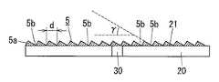
ところで、本実施形態のMEMS光スキャナは、上述のように、可動部形成基板1の可動部20のミラー面21上に回折格子5が形成されている。なお、本実施形態の回折格子5は、ミラー面21上に金属膜(例えば、Al膜など)を成膜した後、フォトリソグラフィ技術およびエッチング技術を利用して当該金属膜を等間隔で平行配置される複数のライン状の金属膜5a(図7参照)にパターニングすることで形成されている。言い換えれば、回折格子5は、可動部20における第1のカバー基板2側に周期的な溝5b(図7参照)を設けることにより形成されており、高い回折効率を得ることができる。また、本実施形態では、回折格子5の溝5bの形状(溝形状)を矩形状(断面矩形状)としてあるので、回折格子5を容易に形成することができる。なお、本実施形態では、回折格子5の格子周期をd(図7参照)とすると、走査対象(スキャン対象)の光の波長や入射角に基づいて、格子周期dを2μm〜20μm程度の範囲で適宜設定すればよい。  By the way, in the MEMS optical scanner of this embodiment, thediffraction grating 5 is formed on themirror surface 21 of themovable part 20 of the movablepart forming substrate 1 as described above. In thediffraction grating 5 of the present embodiment, after a metal film (for example, an Al film) is formed on themirror surface 21, the metal film is arranged in parallel at equal intervals using a photolithography technique and an etching technique. It is formed by patterning a plurality of line-shapedmetal films 5a (see FIG. 7). In other words, thediffraction grating 5 is formed by providing theperiodic groove 5b (see FIG. 7) on thefirst cover substrate 2 side in themovable portion 20, and high diffraction efficiency can be obtained. In the present embodiment, since the shape (groove shape) of thegroove 5b of thediffraction grating 5 is rectangular (cross-sectional rectangular shape), thediffraction grating 5 can be easily formed. In the present embodiment, when the grating period of thediffraction grating 5 is d (see FIG. 7), the grating period d is in the range of about 2 μm to 20 μm based on the wavelength and incident angle of the light to be scanned (scanned object). And set as appropriate.

ところで、図3に示すように、回折格子5に入射光が入射すると、回折格子5からは各次数(回折の次数)の回折光が出射される。図3には、0次の回折光(反射光)、1次の回折光、2次の回折光、−1次の回折光、−2次の回折光、−3次の回折光のみ図示してあるが、本実施形態では、0次の回折光に比べて光学振れ角を大きくできる−1次の回折光を走査光として第1のカバー基板2から出射させるようにしてある。具体的には、第1のカバー基板2には、入射光を透過させる入射光透過部203と、−1次の回折光からなる走査光を透過させる走査光透過部204とが各別に設けられている。ここで、第1のカバー基板2は、第1のガラス基板200における可動部形成基板1側とは反対側の表面のうち、入射光透過部203および走査光透過部204それぞれに対応する部位以外の領域に、金属膜などからなる遮光膜(図示せず)を、蒸着法やスパッタ法やめっき法などを利用して形成してある。要するに、本実施形態では、第1のカバー基板2が、入射光および、回折格子の法線に対して入射光とは反対側にある負の次数の回折光のうち規定次数の回折光以外を遮光するカバー基板を構成している。なお、上記遮光膜の材料としては、光の吸収率の高い材料を採用する方が光の多重反射に起因した迷光を低減する点で好ましく、金属以外の材料により形成してもよい。  As shown in FIG. 3, when incident light enters thediffraction grating 5, thediffraction grating 5 emits diffracted light of each order (diffraction order). FIG. 3 shows only 0th-order diffracted light (reflected light), 1st-order diffracted light, 2nd-order diffracted light, −1st-order diffracted light, −2nd-order diffracted light, and −3rd-order diffracted light. However, in the present embodiment, −1st order diffracted light that can have an optical deflection angle larger than that of 0th order diffracted light is emitted from thefirst cover substrate 2 as scanning light. Specifically, thefirst cover substrate 2 is provided with an incidentlight transmitting portion 203 that transmits incident light and a scanninglight transmitting portion 204 that transmits scanning light composed of −1st order diffracted light. ing. Here, thefirst cover substrate 2 is a portion other than the portion corresponding to each of the incidentlight transmitting portion 203 and the scanninglight transmitting portion 204 on the surface of thefirst glass substrate 200 opposite to the movableportion forming substrate 1 side. In this region, a light shielding film (not shown) made of a metal film or the like is formed by using a vapor deposition method, a sputtering method, a plating method, or the like. In short, in the present embodiment, thefirst cover substrate 2 is configured such that incident light and negative order diffracted light other than the incident light with respect to the normal line of the diffraction grating are other than the prescribed order diffracted light. A cover substrate for shielding light is configured. As the material for the light-shielding film, it is preferable to use a material having a high light absorptivity from the viewpoint of reducing stray light due to multiple reflection of light, and it may be formed of a material other than metal.

本実施形態では、入射透過部203および走査光透過部204を、第1のガラス基板200の一部により構成しているが、入射透過部203および走査光透過部204は、それぞれ第1のガラス基板200の厚み方向に貫通する透孔により構成してもよいし、当該透孔に、走査対象の光に対して透明な材料を充填して形成してもよい。なお、第1のカバー基板2は、第1のガラス基板200に限らず、例えば、アクリル基板や金属板を用いて形成してもよく、アクリル基板を用いて形成する場合には、第1のガラス基板200を用いて形成する場合と同様に上記遮光膜を設けることで入射透過部203および走査光透過部204を形成してもよいし、入射透過部203および走査光透過部204それぞれに対応する部位に透孔を貫設してもよいし、当該透孔に、走査対象の光に対して透明な材料を充填して形成してもよく、また、金属板を用いて形成する場合には、入射透過部203および走査光透過部204それぞれに対応する部位に透孔を貫設してもよいし、当該透孔に、走査対象の光に対して透明な材料を充填して形成してもよい。  In the present embodiment, theincident transmission part 203 and the scanninglight transmission part 204 are configured by a part of thefirst glass substrate 200. However, theincident transmission part 203 and the scanninglight transmission part 204 are each a first glass. You may comprise by the through-hole penetrated in the thickness direction of the board |substrate 200, and you may fill and form the said through-hole with the material transparent with respect to the light of scanning object. Thefirst cover substrate 2 is not limited to thefirst glass substrate 200, and may be formed using, for example, an acrylic substrate or a metal plate. As in the case of forming using theglass substrate 200, the light-shielding film may be provided to form the incidenttransmissive part 203 and the scanning lighttransmissive part 204, or corresponding to the incidenttransmissive part 203 and the scanning lighttransmissive part 204, respectively. A through-hole may be provided in a portion to be formed, or the through-hole may be formed by filling a material transparent to the light to be scanned, or when using a metal plate May be formed by penetrating through holes at portions corresponding to theincident transmitting portion 203 and the scanninglight transmitting portion 204, respectively, and filling the through holes with a material transparent to the light to be scanned. May be.

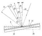
ここで、図4に示すように、回折格子5の法線に対する光の入射角をα、回折角をβ、回折の次数をκ(κ=0,±1,±2,・・・)、回折格子5の格子周期をdとすると、回折角βは、下記(1)式で与えられる。  Here, as shown in FIG. 4, the incident angle of light with respect to the normal line of thediffraction grating 5 is α, the diffraction angle is β, the order of diffraction is κ (κ = 0, ± 1, ± 2,...), If the grating period of thediffraction grating 5 is d, the diffraction angle β is given by the following equation (1).

Figure 2011118179
Figure 2011118179

ここで、次数κが0の場合の回折角βは、入射角αと等しくなる。すなわち、0次の回折光である反射光は、入射光と等しい角度で出射される。これに対して、0次以外の回折光は、入射光よりも大きい角度あるいは小さい角度で出射されることとなる。本実施形態では、入射光よりも大きい角度で出射される回折光、すなわち、負の次数の回折光のうち規定次数(ここでは、−1)の回折光を走査光として上述の走査光透過部204から出射させる。  Here, the diffraction angle β when the order κ is 0 is equal to the incident angle α. That is, the reflected light that is 0th-order diffracted light is emitted at an angle equal to the incident light. On the other hand, diffracted light other than the 0th order is emitted at an angle larger or smaller than the incident light. In the present embodiment, the above-described scanning light transmission unit uses the diffracted light emitted at an angle larger than the incident light, that is, the diffracted light of the specified order (here, −1) out of the negative order diffracted light as the scanning light. The light is emitted from 204.

ここにおいて、可動部20が図4中に一点鎖線で示したように水平な状態から角度θmだけ回動して同図中に実線で示したように左下がりの状態に傾いたとすると、0次の回折光(反射光)、0次以外の回折光それぞれの光学振れ角θr,θdは、下記(2)式、下記(3)式で与えられる。Here, if themovable portion 20 is rotated by an angle θm from a horizontal state as shown by a one-dot chain line in FIG. 4 and tilted to a lower left state as shown by a solid line in FIG. The optical deflection angles θr and θd of the next diffracted light (reflected light) and diffracted light other than the 0th order are given by the following equations (2) and (3).

Figure 2011118179
Figure 2011118179

いま、一例として、0次以外の回折光の次数κを−1、光の波長λを633nm、回折格子5の格子周期dを5μm、入射角α0を35°とすると、可動部20の機械振れ角(θm)と光学振れ角θr,θdとの関係は図5の破線イ、実線ロのようになる。この図5から、−1次の回折光を利用することにより、0次の回折光(反射光)を利用するよりも、大きな光学振れ角を得ることができることが分かる。ここで、走査光として用いる回折光の次数は、適宜選択すればよいが、反射光に比べて回折角が極端に大きな回折光は走査光として利用することが難しいので、上記規定次数は、−1もしくは−2が好ましい。なお、上述の光の波長λ、格子周期d、入射角の数値は一例であって、これらの数値は特に限定するものではない。As an example, if the order κ of diffracted light other than the 0th order is −1, the wavelength λ of the light is 633 nm, the grating period d of thediffraction grating 5 is 5 μm, and the incident angle α0 is 35 °, the machine of themovable unit 20 The relationship between the deflection angle (θm ) and the optical deflection angles θr and θd is as shown by the broken line a and the solid line B in FIG. From FIG. 5, it can be seen that by using the −1st order diffracted light, a larger optical deflection angle can be obtained than when using the 0th order diffracted light (reflected light). Here, the order of the diffracted light used as the scanning light may be appropriately selected. However, since the diffracted light having an extremely large diffraction angle as compared with the reflected light is difficult to use as the scanning light, the specified order is − 1 or -2 is preferred. The numerical values of the wavelength λ, the grating period d, and the incident angle described above are merely examples, and these numerical values are not particularly limited.

ところで、回折格子5の溝5bの延長方向(格子周期方向に直交する方向)が一対の捩りばね部30,30の並設方向に平行な場合、一対の捩りばね部30,30の並設方向に直交する平面(xz平面)に沿って回折格子5に入射光を入射させると、全ての回折光が同一平面(xz平面)上に存在することとなり、MEMS光スキャナの走査光として必要な光のみを出射させることが困難となる。  By the way, when the extending direction of thegroove 5b of the diffraction grating 5 (the direction orthogonal to the grating periodic direction) is parallel to the parallel direction of the pair oftorsion spring portions 30, 30, the parallel direction of the pair oftorsion spring portions 30, 30 When incident light is incident on thediffraction grating 5 along a plane orthogonal to (xz plane), all the diffracted light exists on the same plane (xz plane), and light necessary as scanning light for the MEMS optical scanner It becomes difficult to emit only the light.

これに対して、本実施形態のMEMS光スキャナでは、図6に示すように、可動部20の機械振れ角が0°の状態で当該回折格子5の中心に立てた法線がz軸上にある一方で、一対の捩りばね部30,30がy軸上にあり、回折格子5の溝5bの延長方向(回折格子5の格子周期方向に直交する方向)を、xy平面においてy軸に対して反時計周り方向に所定角φだけ傾けてある。なお、所定角φはxy平面においてy軸に対して反時計周り方向を正としてあるが、所定角φは負でもよい(つまり、溝5bの延長方向はxy平面においてy軸に対して時計回り方向に傾けてもよい)。  On the other hand, in the MEMS optical scanner of the present embodiment, as shown in FIG. 6, the normal line set up at the center of thediffraction grating 5 with the mechanical deflection angle of themovable part 20 being 0 ° is on the z axis. On the other hand, the pair of torsion springs 30 and 30 are on the y-axis, and the extending direction of thegroove 5b of the diffraction grating 5 (the direction perpendicular to the grating period direction of the diffraction grating 5) is set to the y-axis in the xy plane. Thus, it is tilted by a predetermined angle φ in the counterclockwise direction. The predetermined angle φ is positive in the counterclockwise direction with respect to the y axis in the xy plane, but the predetermined angle φ may be negative (that is, the extension direction of thegroove 5b is clockwise with respect to the y axis in the xy plane). Can be tilted in the direction).

要するに、本実施形態における回折格子5は、平面視において格子周期方向に直交する方向を、一対の捩りばね部30,30の並設方向に対して非平行としてある。しかして、一対の捩りばね部30,30の並設方向に直交する平面に沿って回折格子5に入射光を入射させて用いる場合に、回折格子5からの0次の回折光を当該平面に沿って進行させて第1のカバー基板2で遮光する一方で、上記規定次数(−1あるいは−2)の回折光を当該平面から傾いた面に沿って進行させ第1のカバー基板2から出射させることができる。なお、所定角φは、上記規定次数の回折光と他の回折光とを分離できるように適宜設定すればよいが、10°以下で設定することが好ましい。  In short, thediffraction grating 5 in the present embodiment has a direction orthogonal to the grating periodic direction in plan view that is not parallel to the parallel arrangement direction of the pair oftorsion spring portions 30 and 30. Thus, when incident light is incident on thediffraction grating 5 along a plane perpendicular to the direction in which the pair oftorsion spring portions 30 and 30 are juxtaposed, the 0th-order diffracted light from thediffraction grating 5 is applied to the plane. Thefirst cover substrate 2 is shielded from light by thefirst cover substrate 2 while the diffracted light of the specified order (−1 or −2) travels along a plane inclined from the plane and is emitted from thefirst cover substrate 2. Can be made. The predetermined angle φ may be set as appropriate so that the diffracted light of the specified order and other diffracted light can be separated, but is preferably set at 10 ° or less.

以下、本実施形態のMEMS光スキャナの製造方法について図8を参照しながら説明するが、(a)〜(d)は図2(a)のA−B’断面に対応する部分の概略断面を示している。  Hereinafter, the manufacturing method of the MEMS optical scanner of the present embodiment will be described with reference to FIG. 8. FIGS. 8A to 8D are schematic cross-sectional views corresponding to the cross-section AB ′ of FIG. Show.

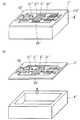
まず、半導体基板であるSOI基板100の上記一表面側に所定膜厚(例えば、500nm)の金属膜(例えば、Al膜など)をスパッタ法や蒸着法などにより成膜する金属膜形成工程を行い、フォトリソグラフィ技術およびエッチング技術を利用して金属膜をパターニングすることにより各パッド13,13および回折格子5を形成する金属膜パターニング工程を行うことによって、図8(a)に示す構造を得る。なお、本実施形態では、各パッド13,13と回折格子5のライン状の金属膜5a(図7参照)との材料および膜厚を同じに設定してあるので、各パッド13,13と回折格子5とを同時に形成しているが、各パッド13,13と回折格子5の金属膜5aとの材料や膜厚が相違する場合には、各パッド13,13を形成するパッド形成工程と回折格子5を形成する回折格子形成工程とを別々に設ければよく、パッド形成工程と回折格子形成工程との順序はどちらが先でもよい。  First, a metal film forming step is performed in which a metal film (for example, an Al film) having a predetermined film thickness (for example, 500 nm) is formed on the one surface side of theSOI substrate 100, which is a semiconductor substrate, by sputtering or vapor deposition. By performing a metal film patterning process for forming thepads 13 and 13 and thediffraction grating 5 by patterning the metal film using a photolithography technique and an etching technique, the structure shown in FIG. 8A is obtained. In this embodiment, the materials and film thicknesses of thepads 13 and 13 and the line-shapedmetal film 5a (see FIG. 7) of thediffraction grating 5 are set to be the same. Although thegrating 5 is formed at the same time, if the materials and film thicknesses of thepads 13 and 13 and themetal film 5a of thediffraction grating 5 are different, the pad forming process for forming thepads 13 and 13 and diffraction are performed. The diffraction grating forming process for forming thegrating 5 may be provided separately, and the order of the pad forming process and the diffraction grating forming process may be either.

上述の各パッド13,13および回折格子5を形成した後、SOI基板100の上記一表面側で、第1のシリコン層100aのうち可動部20、一対の捩りばね部30,30、外側フレーム部10、固定電極12,12、可動電極22,22に対応する部位を覆うようにパターニングされた第1のレジスト層130をマスクとして、第1のシリコン層100aを絶縁層100cに達する深さ(第1の所定深さ)までエッチングすることにより第1のシリコン層100aをパターニングする第1のシリコン層パターニング工程(表面側パターニング工程)を行うことによって、図8(b)に示す構造を得る。要するに、第1のシリコン層パターニング工程は、半導体基板であるSOI基板100を上記一表面から第1の所定深さまでエッチングする表面側パターニング工程を構成している。第1のシリコン層パターニング工程での第1のシリコン層100aのエッチングは、誘導結合プラズマ(ICP)型のエッチング装置などの異方性の高いエッチングが可能なドライエッチング装置により行えばよい。また、第1のシリコン層パターニング工程では、絶縁層100cをエッチングストッパ層として利用している。  After forming thepads 13 and 13 and thediffraction grating 5, themovable portion 20, the pair oftorsion spring portions 30 and 30, and the outer frame portion of thefirst silicon layer 100a are formed on the one surface side of theSOI substrate 100. 10. Depth reaching thefirst silicon layer 100a to the insulatinglayer 100c using the first resistlayer 130 patterned so as to cover the portions corresponding to the fixedelectrodes 12 and 12 and themovable electrodes 22 and 22 (a first thickness). The structure shown in FIG. 8B is obtained by performing a first silicon layer patterning step (surface side patterning step) for patterning thefirst silicon layer 100a by etching to a predetermined depth of 1). In short, the first silicon layer patterning step constitutes a surface side patterning step of etching theSOI substrate 100, which is a semiconductor substrate, from the one surface to a first predetermined depth. Etching of thefirst silicon layer 100a in the first silicon layer patterning step may be performed by a dry etching apparatus capable of highly anisotropic etching such as an inductively coupled plasma (ICP) type etching apparatus. In the first silicon layer patterning step, the insulatinglayer 100c is used as an etching stopper layer.

上述の第1のシリコン層パターニング工程の後、SOI基板100の上記一表面側の第1のレジスト層130を除去してから、SOI基板100の上記一表面側の全面に第2のレジスト層131を形成し、続いて、SOI基板100の他表面側で、第2のシリコン層100bのうち外側フレーム部10に対応する部位以外を露出させるようにパターニングされた第3のレジスト層132をマスクとして、第2のシリコン層100bを絶縁層100cに達する深さ(第2の所定深さ)までエッチングすることにより第2のシリコン層100bをパターニングする第2のシリコン層パターニング工程を行うことによって、図8(c)に示す構造を得る。要するに、第2のシリコン層パターニング工程は、半導体基板であるSOI基板100を上記他表面から第2の所定深さまでエッチングする裏面側パターニング工程を構成している。第2のシリコン層パターニング工程での第2のシリコン層100bのエッチングは、誘導結合プラズマ(ICP)型のエッチング装置などの異方性が高く垂直深堀が可能なドライエッチング装置により行えばよい。また、第2のシリコン層パターニング工程では、絶縁層100cをエッチングストッパ層として利用している。  After the first silicon layer patterning step, the first resistlayer 130 on the one surface side of theSOI substrate 100 is removed, and then the second resistlayer 131 is formed on the entire surface on the one surface side of theSOI substrate 100. Then, on the other surface side of theSOI substrate 100, the third resistlayer 132 patterned so as to expose thesecond silicon layer 100b other than the portion corresponding to theouter frame portion 10 is used as a mask. By performing a second silicon layer patterning step of patterning thesecond silicon layer 100b by etching thesecond silicon layer 100b to a depth (second predetermined depth) reaching the insulatinglayer 100c, FIG. The structure shown in 8 (c) is obtained. In short, the second silicon layer patterning step constitutes a back side patterning step of etching theSOI substrate 100, which is a semiconductor substrate, from the other surface to a second predetermined depth. Etching of thesecond silicon layer 100b in the second silicon layer patterning step may be performed by a dry etching apparatus that has high anisotropy and enables vertical deepening, such as an inductively coupled plasma (ICP) etching apparatus. In the second silicon layer patterning step, the insulatinglayer 100c is used as an etching stopper layer.

上述の第2のシリコン層パターニング工程の後、SOI基板100の絶縁層100cにおいて外側フレーム部10と可動部20との間の部位、可動電極22,22と固定電極12,12との間の部位を、SOI基板100の上記他表面側からエッチングする絶縁層パターニング工程を行うことで可動部形成基板1を形成してから、第2のレジスト層131および第3のレジスト層132を除去し、その後、可動部形成基板1と、第1のカバー基板2および第2のカバー基板3とを陽極接合などにより接合する接合工程を行うことによって、図8(d)に示す構造のMEMS光スキャナを得る。  After the above-described second silicon layer patterning step, a portion between theouter frame portion 10 and themovable portion 20 and a portion between themovable electrodes 22, 22 and the fixedelectrodes 12, 12 in the insulatinglayer 100c of theSOI substrate 100. After forming the movablepart forming substrate 1 by performing an insulating layer patterning step of etching from the other surface side of theSOI substrate 100, the second resistlayer 131 and the third resistlayer 132 are removed, and then Then, the MEMS optical scanner having the structure shown in FIG. 8D is obtained by performing a bonding step of bonding the movableportion forming substrate 1 to thefirst cover substrate 2 and thesecond cover substrate 3 by anodic bonding or the like. .

ここにおいて、接合工程では、可動部形成基板1のミラー面21を保護する観点から、第1のカバー基板2と可動部形成基板1とを接合する第1の接合過程を行ってから、可動部形成基板1と第2のカバー基板3とを接合する第2の接合過程を行うことが好ましい。ここで、第1の接合過程では、先ず、第1のガラス基板200に第1の変位空間形成用凹部201や各貫通孔202,202を形成した第1のカバー基板2と可動部形成基板1とを重ねた積層体を、所定真空度(例えば、10Pa以下)の真空中で所定の接合温度(例えば、300℃〜400℃程度)に加熱した状態で、第1のシリコン層100aと第1のカバー基板2との間に第1のカバー基板2側を低電位側として所定電圧(例えば、400V〜800V程度)を印加し、この状態を所定の接合時間(例えば、20分〜60分程度)だけ保持すればよい。また、第2の接合過程では、上述の第1の接合過程に準じて、第2のシリコン層100bと第2のカバー基板3との陽極接合を行う。なお、可動部形成基板1と各カバー基板2,3を接合する接合方法は、陽極接合に限らず、例えば、常温接合法などでもよい。また、第1のシリコン層パターニング工程の後に、SOI基板100と第1のカバー基板2とを接合し、その後、第2のシリコン層パターニング工程、絶縁層パターニング工程を行うことで可動部形成基板1を形成し、その後、可動部形成基板1と第2のカバー基板3とを接合するようにしてもよい。  Here, in the joining step, from the viewpoint of protecting themirror surface 21 of the movablepart forming substrate 1, a first joining process for joining thefirst cover substrate 2 and the movablepart forming substrate 1 is performed, and then the movable part. It is preferable to perform a second bonding process for bonding theformation substrate 1 and thesecond cover substrate 3 together. Here, in the first bonding process, first, thefirst cover substrate 2 and the movableportion forming substrate 1 in which the first displacementspace forming recesses 201 and the throughholes 202 and 202 are formed in thefirst glass substrate 200. And thefirst silicon layer 100a and the first layer are heated in a vacuum at a predetermined degree of vacuum (for example, 10 Pa or less) to a predetermined bonding temperature (for example, about 300 ° C. to 400 ° C.). A predetermined voltage (for example, about 400V to 800V) is applied between thefirst cover substrate 2 and thecover substrate 2 with thefirst cover substrate 2 side as a low potential side, and this state is maintained for a predetermined bonding time (for example, about 20 minutes to 60 minutes). Only hold). In the second bonding process, anodic bonding between thesecond silicon layer 100b and thesecond cover substrate 3 is performed in accordance with the first bonding process described above. Note that the bonding method for bonding the movableportion forming substrate 1 and thecover substrates 2 and 3 is not limited to anodic bonding, and may be, for example, a room temperature bonding method. In addition, after the first silicon layer patterning step, theSOI substrate 100 and thefirst cover substrate 2 are bonded together, and then the second silicon layer patterning step and the insulating layer patterning step are performed, whereby the movablepart forming substrate 1. After that, the movablepart forming substrate 1 and thesecond cover substrate 3 may be bonded to each other.

ところで、本実施形態のMEMS光スキャナの製造方法では、接合工程が終了するまでの全工程を可動部形成基板1および各カバー基板2,3それぞれについてウェハレベルで行うことでMEMS光スキャナを複数備えたウェハレベルパッケージ構造体を形成するようにし、当該ウェハレベルパッケージ構造体から個々のMEMS光スキャナに分割する分割工程を行うようにしている。要するに、本実施形態のMEMS光スキャナの製造方法では、可動部形成基板1を複数形成した第1のウェハと、第1のカバー基板2を複数形成した第2のウェハおよび第2のカバー基板3を複数形成した第3のウェハとを接合することでウェハレベルパッケージ構造体を形成した後、ウェハレベルパッケージ構造体から可動部形成基板1の外形サイズに分割するようにしているので、各カバー基板2,3の平面サイズを可動部形成基板1の外形サイズに合わせることができるから、小型で光学振れ角が大きなMEMS光スキャナを簡易なプロセスで製造することができ、また、量産性を高めることができる。  By the way, in the manufacturing method of the MEMS optical scanner according to the present embodiment, a plurality of MEMS optical scanners are provided by performing all the processes until the joining process is completed on the movablepart forming substrate 1 and each of thecover substrates 2 and 3 at the wafer level. A wafer level package structure is formed, and a dividing step of dividing the wafer level package structure into individual MEMS optical scanners is performed. In short, in the manufacturing method of the MEMS optical scanner of the present embodiment, the first wafer on which a plurality of movablepart forming substrates 1 are formed, the second wafer on which a plurality offirst cover substrates 2 are formed, and thesecond cover substrate 3. After the wafer level package structure is formed by joining the third wafer formed with a plurality of wafers, the wafer level package structure is divided into the outer size of the movablepart forming substrate 1. Since the planar size of 2 or 3 can be adjusted to the external size of the movablepart forming substrate 1, a small-sized MEMS optical scanner having a large optical deflection angle can be manufactured by a simple process, and mass productivity can be improved. Can do.

以上説明した本実施形態のMEMS光スキャナでは、可動部形成基板1の可動部20のミラー面21側に回折格子5が形成されており、入射光および、回折格子5の法線に対して入射光とは反対側にある負の次数の回折光のうち規定次数の回折光以外を遮光する第1のカバー基板2が可動部形成基板1に接合されているので、光学振れ角を大きくすることが可能で且つ不要な光が出射されるのを防止することが可能となる。ここにおいて、本実施形態のMEMS光スキャナでは、上記規定次数を−1としてあるので、−1次の回折光を走査光として出射することとなり、走査光の光学振れ角が大きくなりすぎて第1のカバー基板2の平面サイズが大きくなって小型化が制限されるのを防止することができるとともに、−2次以上の回折光を走査光として利用する場合に比べて走査光の光強度を高めることができる。  In the MEMS optical scanner of the present embodiment described above, thediffraction grating 5 is formed on themirror surface 21 side of themovable part 20 of the movablepart forming substrate 1, and is incident on the incident light and the normal line of thediffraction grating 5. Since thefirst cover substrate 2 that shields the diffracted light of negative order other than the diffracted light of the negative order on the side opposite to the light is joined to the movablepart forming substrate 1, the optical deflection angle is increased. It is possible to prevent unnecessary light from being emitted. Here, in the MEMS optical scanner of the present embodiment, since the specified order is −1, the −1st order diffracted light is emitted as scanning light, and the optical deflection angle of the scanning light becomes too large, and the first order. It is possible to prevent the size of thecover substrate 2 from becoming large and restricting downsizing, and to increase the light intensity of the scanning light as compared with the case where diffracted light of −2nd order or higher is used as the scanning light. be able to.

また、本実施形態のMEMS光スキャナでは、回折格子5は、可動部20のミラー面21側に周期的な溝5bを設けることにより形成されているので、高い回折効率を得ることができる。  Further, in the MEMS optical scanner of the present embodiment, thediffraction grating 5 is formed by providing theperiodic groove 5b on themirror surface 21 side of themovable portion 20, so that high diffraction efficiency can be obtained.

また、本実施形態のMEMS光スキャナでは、SOI基板100の第1のシリコン層100aにより各捩りばね部30,30を形成してあるので、半導体基板としてシリコン基板を用いる場合に比べて各捩りばね部30,30の厚み寸法の精度を高めることができ、可動部20と一対の捩りばね部30,30とで構成される振動系の共振周波数の精度を高めることができる。  In the MEMS optical scanner of this embodiment, the torsion springs 30 and 30 are formed by thefirst silicon layer 100a of theSOI substrate 100. Therefore, each torsion spring is compared with a case where a silicon substrate is used as the semiconductor substrate. The precision of the thickness dimension of theparts 30 and 30 can be raised, and the precision of the resonant frequency of the vibration system comprised by themovable part 20 and a pair oftorsion spring parts 30 and 30 can be raised.

ところで、回折格子5の溝5bの形状である溝形状を矩形状としてあるが、図9に示すように、溝5bの形状である溝形状を鋸歯状とすれば、回折格子5の回折効率をより高めることができる。ここで、溝5bの周期(格子周期)dおよび鋸歯面の角度γは、走査対象の光の波長や入射角に基づいて適宜設定すればよい。ただし、図7に示したように、溝5bの溝形状を矩形状とした方が、鋸歯状の場合に比べて、回折格子5を容易に形成することができる。ここで、溝形状が鋸歯状の溝5bを形成するには、例えば、インプリント法を利用して鋸歯状の溝形状に対応する断面形状のエッチングマスク層を形成してから、エッチングを行うようにしたり、フォトリソグラフィ工程とエッチング工程とを繰り返し行うことで所定レベル(階調数)の階段構造を形成するようにしてもよい(例えば、16レベルの階段構造を有する回折格子5を形成するようにしてもよい)。なお、回折格子5の溝5bの形状は特に矩形状や鋸歯状に限らず、周期的に溝5bが形成されていればよい。また、回折格子5は、可動部20に直接形成してもよい(第1のシリコン層100aに溝5bを形成することで形成してもよい)。  By the way, although the groove shape which is the shape of thegroove 5b of thediffraction grating 5 is rectangular, as shown in FIG. 9, if the groove shape which is the shape of thegroove 5b is serrated, the diffraction efficiency of thediffraction grating 5 is improved. Can be increased. Here, the period (grating period) d of thegroove 5b and the angle γ of the sawtooth surface may be set as appropriate based on the wavelength and incident angle of the light to be scanned. However, as shown in FIG. 7, thediffraction grating 5 can be formed more easily when the groove shape of thegroove 5 b is rectangular than when the groove shape is a sawtooth shape. Here, in order to form thegroove 5b having a serrated groove shape, for example, an etching mask layer having a cross-sectional shape corresponding to the sawtooth groove shape is formed by using an imprint method, and then etching is performed. Or a step structure having a predetermined level (the number of gradations) may be formed by repeatedly performing a photolithography process and an etching process (for example, thediffraction grating 5 having a 16-level step structure may be formed). It may be) In addition, the shape of thegroove 5b of thediffraction grating 5 is not limited to a rectangular shape or a sawtooth shape, and thegroove 5b may be formed periodically. Thediffraction grating 5 may be formed directly on the movable portion 20 (may be formed by forming thegroove 5b in thefirst silicon layer 100a).

また、回折格子5は、図9に示すように、相対的に反射率の高い材料からなるライン状の高反射率膜たる金属膜5aと相対的に反射率の低い材料からなるライン状の低反射率膜たるSiO膜5cとがミラー面21に沿って交互に配列された構成としてもよく、この場合も、回折格子5を容易に形成することができる。ここで、低反射率膜がSiO膜5cからなり、高反射率膜が金属膜5aであることにより、回折格子5を一般的なMEMSプロセスとの整合性の良いプロセスで形成することができる。なお、高反射率膜として用いる金属膜としては、Al−Si膜、Al膜、Au膜などを採用すれば、反射率が高く且つ膜質のよい薄膜を得ることができるが、低反射率膜と高反射率膜との材料の組み合わせは、走査対象の光の波長に応じて適宜決定すればよい。Further, as shown in FIG. 9, thediffraction grating 5 is composed of a line-shaped low film made of a material having a relatively low reflectivity and ametal film 5a that is a line-shaped high reflectivity film made of a material having a relatively high reflectivity. The configuration may be such that the SiO2 film 5c, which is a reflectance film, is alternately arranged along themirror surface 21, and also in this case, thediffraction grating 5 can be easily formed. Here, since the low reflectance film is made of the SiO2 film 5c and the high reflectance film is themetal film 5a, thediffraction grating 5 can be formed by a process having good consistency with a general MEMS process. . As the metal film used as the high reflectivity film, if an Al-Si film, an Al film, an Au film, or the like is employed, a thin film having high reflectivity and good film quality can be obtained. What is necessary is just to determine the combination of a material with a high reflectance film | membrane suitably according to the wavelength of the light of scanning object.

また、本実施形態のMEMS光スキャナにおいて、各パッド13それぞれの代わりに、例えば、第1のカバー基板2の外表面と可動部形成基板1における外側フレーム部10の表面と貫通孔202の内側面とに跨って形成された貫通配線を外部接続電極として形成してもよい。  Further, in the MEMS optical scanner of the present embodiment, instead of eachpad 13, for example, the outer surface of thefirst cover substrate 2, the surface of theouter frame portion 10 in the movableportion forming substrate 1, and the inner surface of the throughhole 202. A through-wiring formed over the two may be formed as an external connection electrode.

1 可動部形成基板
2 第1のカバー基板(カバー基板)
5 回折格子
5a 金属膜(高反射率膜)
5b 溝
5c SiO膜(低反射率膜)
12 固定電極
20 可動部
21 ミラー面
22 可動電極
30 捩りばね部
100 SOI基板(半導体基板)
200 第1のガラス基板
203 入射光透過部
204 走査光透過部
1 movablepart formation board 2 1st cover board (cover board)
5 Diffraction grating 5a Metal film (High reflectivity film)
5b groove 5c SiO2 film (low reflectance film)
12Fixed Electrode 20Movable Part 21Mirror Surface 22Movable Electrode 30Torsion Spring Part 100 SOI Substrate (Semiconductor Substrate)
200First glass substrate 203 Incidentlight transmission unit 204 Scanning light transmission unit

Claims (8)

Translated fromJapanese
半導体基板を用いて形成され、外側フレーム部、外側フレーム部の内側に配置され一表面側にミラー面が設けられた可動部、および外側フレーム部の内側で可動部を挟む形で配置され外側フレーム部と可動部とを連結し捩れ変形が可能な一対の捩りばね部を有する可動部形成基板と、可動部を駆動する駆動手段とを備えたMEMS光スキャナであって、可動部形成基板の可動部のミラー面側に回折格子が形成されてなり、入射光および、回折格子の法線に対して入射光とは反対側にある負の次数の回折光のうち規定次数の回折光以外を遮光するカバー基板が可動部形成基板に接合されてなることを特徴とするMEMS光スキャナ。  An outer frame formed by using a semiconductor substrate, arranged on the inner side of the outer frame part, the outer frame part and provided with a mirror surface on one surface side, and the outer frame arranged with the movable part sandwiched inside the outer frame part. A MEMS optical scanner comprising a movable part forming substrate having a pair of torsion spring parts that can be torsionally deformed by connecting the part and the movable part, and a driving means for driving the movable part, wherein the movable part forming substrate is movable Diffraction grating is formed on the mirror surface side of the part, shielding incident light and negative order diffracted light on the side opposite to the incident light with respect to the normal of the diffraction grating other than diffracted light of specified order A MEMS optical scanner comprising a cover substrate to be bonded to a movable portion forming substrate. 前記回折格子は、平面視において格子周期方向に直交する方向を、前記各捩りばね部の並設方向に対して非平行としてあることを特徴とする請求項1記載のMEMS光スキャナ。  The MEMS optical scanner according to claim 1, wherein the diffraction grating has a direction orthogonal to the grating periodic direction in plan view that is not parallel to the parallel direction of the torsion spring portions. 前記回折格子は、前記可動部における前記ミラー面側に周期的な溝を設けることにより形成されてなることを特徴とする請求項1または請求項2記載のMEMS光スキャナ。  The MEMS optical scanner according to claim 1, wherein the diffraction grating is formed by providing a periodic groove on the mirror surface side of the movable part. 前記回折格子は、溝形状が鋸歯状であることを特徴とする請求項1ないし請求項3のいずれか1項に記載のMEMS光スキャナ。  4. The MEMS optical scanner according to claim 1, wherein the diffraction grating has a sawtooth shape in a groove shape. 5. 前記回折格子は、前記回折格子は、溝形状が矩形状であることを特徴とする請求項1ないし請求項3のいずれか1項に記載のMEMS光スキャナ。  The MEMS optical scanner according to claim 1, wherein the diffraction grating has a rectangular groove shape. 前記回折格子は、相対的に反射率の高い材料からなるライン状の高反射率膜と相対的に反射率の低い材料からなるライン状の低反射率膜とが前記ミラー面に沿って交互に配列されてなることを特徴とする請求項1記載のMEMS光スキャナ。  The diffraction grating has a line-shaped high reflectance film made of a material having a relatively high reflectance and a line-shaped low reflectance film made of a material having a relatively low reflectance alternately along the mirror surface. The MEMS optical scanner according to claim 1, wherein the MEMS optical scanner is arranged. 前記低反射率膜がSiO膜からなり、前記高反射率膜が金属膜であることを特徴とする請求項6記載のMEMS光スキャナ。The low reflectance film is a SiO2 film, MEMS optical scanner according to claim 6, wherein said high reflectivity film is characterized in that it is a metal film. 前記規定次数が−1であることを特徴とする請求項1ないし請求項7のいずれか1項に記載のMEMS光スキャナ。  The MEMS optical scanner according to claim 1, wherein the specified order is −1.
JP2009275850A2009-12-032009-12-03 MEMS optical scannerExpired - Fee RelatedJP5351729B2 (en)

Priority Applications (1)

Application NumberPriority DateFiling DateTitle
JP2009275850AJP5351729B2 (en)2009-12-032009-12-03 MEMS optical scanner

Applications Claiming Priority (1)

Application NumberPriority DateFiling DateTitle
JP2009275850AJP5351729B2 (en)2009-12-032009-12-03 MEMS optical scanner

Publications (2)

Publication NumberPublication Date
JP2011118179Atrue JP2011118179A (en)2011-06-16
JP5351729B2 JP5351729B2 (en)2013-11-27

Family

ID=44283593

Family Applications (1)

Application NumberTitlePriority DateFiling Date
JP2009275850AExpired - Fee RelatedJP5351729B2 (en)2009-12-032009-12-03 MEMS optical scanner

Country Status (1)

CountryLink
JP (1)JP5351729B2 (en)

Cited By (2)

* Cited by examiner, † Cited by third party
Publication numberPriority datePublication dateAssigneeTitle
JP2019152687A (en)*2018-02-282019-09-12浜松ホトニクス株式会社Movable diffraction grating, external resonator type laser module, and manufacturing method of movable diffraction grating
IT202000016855A1 (en)*2020-07-102022-01-10St Microelectronics Srl MEMS MICROMIRROR DEVICE CLOSED IN A CASING EQUIPPED WITH A TRANSPARENT SURFACE AND HAVING AN ADJUSTABLE PLATFORM

Families Citing this family (1)

* Cited by examiner, † Cited by third party
Publication numberPriority datePublication dateAssigneeTitle
JP6694355B2 (en)2016-09-012020-05-13浜松ホトニクス株式会社 Movable diffraction grating, manufacturing method thereof, and external resonator type laser module

Citations (3)

* Cited by examiner, † Cited by third party
Publication numberPriority datePublication dateAssigneeTitle
JPH07304208A (en)*1994-05-101995-11-21Fuji Electric Co Ltd Light beam deflector
JPH09101468A (en)*1995-10-041997-04-15Matsushita Electric Ind Co Ltd Color type deformable mirror device and projection type image display device
JP2007272066A (en)*2006-03-312007-10-18Brother Ind Ltd Optical scanner and image forming apparatus having the same

Patent Citations (3)

* Cited by examiner, † Cited by third party
Publication numberPriority datePublication dateAssigneeTitle
JPH07304208A (en)*1994-05-101995-11-21Fuji Electric Co Ltd Light beam deflector
JPH09101468A (en)*1995-10-041997-04-15Matsushita Electric Ind Co Ltd Color type deformable mirror device and projection type image display device
JP2007272066A (en)*2006-03-312007-10-18Brother Ind Ltd Optical scanner and image forming apparatus having the same

Cited By (6)

* Cited by examiner, † Cited by third party
Publication numberPriority datePublication dateAssigneeTitle
JP2019152687A (en)*2018-02-282019-09-12浜松ホトニクス株式会社Movable diffraction grating, external resonator type laser module, and manufacturing method of movable diffraction grating
JP7137321B2 (en)2018-02-282022-09-14浜松ホトニクス株式会社 Movable diffraction grating, external cavity laser module, method for manufacturing movable diffraction grating
IT202000016855A1 (en)*2020-07-102022-01-10St Microelectronics Srl MEMS MICROMIRROR DEVICE CLOSED IN A CASING EQUIPPED WITH A TRANSPARENT SURFACE AND HAVING AN ADJUSTABLE PLATFORM
CN113912002A (en)*2020-07-102022-01-11意法半导体股份有限公司 MEMS Micromirror Device
EP3936907A1 (en)2020-07-102022-01-12STMicroelectronics S.r.l.Mems micromirror device enveloped in a package having a transparent surface and having a tiltable platform
US12117608B2 (en)2020-07-102024-10-15Stmicroelectronics S.R.L.MEMS micromirror device enveloped in a package having a transparent surface and having a tiltable platform

Also Published As

Publication numberPublication date
JP5351729B2 (en)2013-11-27

Similar Documents

PublicationPublication DateTitle
JP5452197B2 (en) MEMS optical scanner
JP7154309B2 (en) Micromirror device and driving method of micromirror device
JP6447683B2 (en) Scanning microelectromechanical reflector system, light detection and ranging (LIDAR) device, and method of operating scanning microelectromechanical reflector system
TWI411064B (en) Microelectromechanical system
JP4092283B2 (en) Two-dimensional optical scanner and optical device
JP4409811B2 (en) Optical scanning device, optical writing device, image forming apparatus, vibrating mirror chip, and optical scanning module
US20110188104A1 (en)Moving structure and light scanning mirror using the same
JPWO2013046612A1 (en) Optical reflection element
CN106707415B (en)Adjustable optical device
US11262576B2 (en)Reflective optical element
US9778549B2 (en)Optical element
JP2011112807A (en)Mems optical scanner and method of manufacturing the same
JP2010286609A (en)Mirror structure
JP5351729B2 (en) MEMS optical scanner
JP2011112803A (en)Mems optical scanner
US20090237628A1 (en)Optical reflection device and image projector includng the same
JP5848504B2 (en) Optical deflector
JP2011112806A (en)Mems optical scanner and method of manufacturing the same
JP2012027337A (en)Mems optical scanner
JP2015102709A (en) Optical scanner and image display device
JP2011112804A (en)Mems optical scanner
JP2010060689A (en)Optical reflection element unit
JP2012026935A (en)Sensor apparatus
WO2023105892A1 (en)Optical reflective device
WO2020129708A1 (en)Light reflection element and spatial light modulator

Legal Events

DateCodeTitleDescription
A711Notification of change in applicant

Free format text:JAPANESE INTERMEDIATE CODE: A712

Effective date:20120118

A621Written request for application examination

Free format text:JAPANESE INTERMEDIATE CODE: A621

Effective date:20120911

A977Report on retrieval

Free format text:JAPANESE INTERMEDIATE CODE: A971007

Effective date:20130723

TRDDDecision of grant or rejection written
A01Written decision to grant a patent or to grant a registration (utility model)

Free format text:JAPANESE INTERMEDIATE CODE: A01

Effective date:20130730

A61First payment of annual fees (during grant procedure)

Free format text:JAPANESE INTERMEDIATE CODE: A61

Effective date:20130823

R150Certificate of patent or registration of utility model

Free format text:JAPANESE INTERMEDIATE CODE: R150

A977Report on retrieval

Free format text:JAPANESE INTERMEDIATE CODE: A971007

Effective date:20130917

LAPSCancellation because of no payment of annual fees

[8]ページ先頭

©2009-2025 Movatter.jp