JP2011112388A - Acceleration sensor - Google Patents
Acceleration sensorDownload PDFInfo
- Publication number
- JP2011112388A JP2011112388AJP2009266581AJP2009266581AJP2011112388AJP 2011112388 AJP2011112388 AJP 2011112388AJP 2009266581 AJP2009266581 AJP 2009266581AJP 2009266581 AJP2009266581 AJP 2009266581AJP 2011112388 AJP2011112388 AJP 2011112388A
- Authority
- JP
- Japan
- Prior art keywords
- acceleration sensor
- sensor according
- electrode
- acceleration
- weight
- Prior art date
- Legal status (The legal status is an assumption and is not a legal conclusion. Google has not performed a legal analysis and makes no representation as to the accuracy of the status listed.)
- Granted
Links
Images


Landscapes
- Pressure Sensors (AREA)
Abstract
Translated fromJapaneseDescription
Translated fromJapanese本発明は、静電容量型の加速度センサに関する。 The present invention relates to a capacitance type acceleration sensor.
従来、図5(a)に示すように、可動電極を有する直方体形状の重り部100と、重り部100の長手方向における略中央において重り部100を回動自在に支持する1対のビーム部101と、1対のビーム部101を結ぶ直線を境界線とした重り部100の表面のそれぞれ一方側及び他方側に対して所定距離を空けて対向配置された1対の固定電極102,103とを備えた加速度センサが知られている(例えば、特許文献1参照)。この加速度センサは、前記境界線を回動軸とした重り部100の回動に伴う可動電極(重り部100における固定電極102,103との対向部位)と、固定電極102,103との間の静電容量の変化を差動検出することにより、重り部100に印加された加速度を検出する。このような加速度センサでは、重り部100の裏面の前記境界線を挟んだ一方側(図5(a)における右側)に凹部104を形成することにより、重り部100は前記境界線を挟んだ一方側(右側)と他方側(左側)とで重量が異なるように構成している。而して、加速度が印加された際に前記境界線を回動軸としたモーメントが重り部100に発生するようになっている。ここで、重り部100の凹部104が形成された部位が周囲からの応力によって変形してしまうのを防ぐために、凹部104内を2分割するような補強壁105を前記境界線と平行な向きに沿って重り部100と一体に形成している。 Conventionally, as shown in FIG. 5A, a rectangular
ところで、上記の加速度センサでは、回動軸に直交する2方向の加速度を検出することができるが、重り部100の重心位置から回動軸に下ろした垂線と重り部100の表面とが成す角度θを略45度に設定することによって、これら2方向の検出感度を等価にしている。ここで、加速度センサの検出感度を向上させる手段の一つとして、可動電極の面積を大きくする方法があるが、この方法を採用する場合には上記の角度θを略45度に維持するために重り部100の厚み寸法を大きくしなければならない。重り部100の厚み寸法を大きくすると、重り部100を形成するエッチング工程の時間が長くなるため、現実的ではないという問題があった。 By the way, although the acceleration sensor described above can detect acceleration in two directions orthogonal to the rotation axis, an angle formed by a perpendicular line drawn from the center of gravity of the
そこで、重り部100の厚み寸法を大きくすることなく上記の角度θを略45度に維持させるために、図5(b)に示すように、重り部100におけるビーム部101の同図における直下を刳り貫く事で重り部100を軽量化する方法がある。しかしながら、この方法を採用する場合には、重り部100において軽量化された薄肉部の強度が不足するために好ましくないという問題があった。 Therefore, in order to maintain the above angle θ at about 45 degrees without increasing the thickness dimension of the
本発明は、上記の点に鑑みて為されたもので、重り部の厚み寸法の大型化や軽量化をすることなく検出感度を向上させることのできる加速度センサを提供することを目的とする。 The present invention has been made in view of the above points, and an object of the present invention is to provide an acceleration sensor capable of improving detection sensitivity without increasing the thickness or weight of the weight portion.
請求項1の発明は、上記目的を達成するために、一面に開口する凹部と凹部を除く充実部が一体に形成された重り部と、凹部と充実部とが回動方向に沿って並ぶように重り部を回動自在に支持する1対のビーム部と、凹部が開口する前記一面と異なる他の一面において凹部と充実部とに跨って設けられた可動電極と、可動電極における凹部側と対向する位置に配設された第1の固定電極と、可動電極における充実部側と対向する位置に配設された第2の固定電極とから成るセンサ部を備え、1対のビーム部を結ぶ直線を回動軸とした重り部の回動に伴う可動電極と固定電極との間の静電容量の変化から加速度を検出する加速度センサであって、重り部の重心位置から前記回動軸に下ろした垂線と可動電極の表面とが成す角度が略45度となるように、ビーム部を凹部側にずらして配置したことを特徴とする。 In order to achieve the above object, the first aspect of the present invention is such that the concave portion opening on one surface and the weight portion integrally formed with the solid portion excluding the concave portion, and the concave portion and the solid portion are aligned along the rotation direction. A pair of beam portions that rotatably support the weight portion, a movable electrode provided across the concave portion and the solid portion on the other surface different from the one surface where the concave portion opens, and the concave portion side of the movable electrode; A sensor unit comprising a first fixed electrode disposed at an opposing position and a second fixed electrode disposed at a position facing the solid portion side of the movable electrode is provided, and a pair of beam portions are connected. An acceleration sensor that detects acceleration from a change in capacitance between the movable electrode and the fixed electrode that accompanies the rotation of the weight portion with a straight axis as the rotation axis, and that detects the acceleration from the center of gravity of the weight portion to the rotation axis. The angle formed by the lowered perpendicular and the surface of the movable electrode is approximately 45 degrees. Sea urchin, characterized in that arranged by shifting the beam portion to the concave side.
請求項2の発明は、請求項1の発明において、重り部に印加された第1の方向の加速度と、第1の方向と直交する第2の方向の加速度とを検出することを特徴とする。 The invention of claim 2 is characterized in that, in the invention of
請求項3の発明は、請求項2の発明において、センサ部は、同一のチップに複数形成されることを特徴とする。 According to a third aspect of the present invention, in the second aspect of the present invention, a plurality of sensor portions are formed on the same chip.
請求項4の発明は、請求項3の発明において、センサ部が同一のチップに2つ形成され、一方のセンサ部が他方のセンサ部に対して同一平面において180度回転して配置されたことを特徴とする。 According to a fourth aspect of the present invention, in the third aspect of the present invention, two sensor portions are formed on the same chip, and one sensor portion is rotated 180 degrees in the same plane with respect to the other sensor portion. It is characterized by.
請求項5の発明は、請求項4の発明において、2つのセンサ部が隣接して配置されたことを特徴とする。 The invention of
請求項6の発明は、請求項3の発明において、センサ部は同一のチップに3つ形成され、2つのセンサ部は、それぞれ残りの1つのセンサ部に対して同一平面において90度及び180度回転して配置されたことを特徴とする。 According to a sixth aspect of the present invention, in the third aspect of the present invention, three sensor portions are formed on the same chip, and the two sensor portions are respectively 90 degrees and 180 degrees in the same plane with respect to the remaining one sensor portion. It is characterized by being rotated.
請求項7の発明は、請求項1乃至6の何れか1項の発明において、重り部を内包する枠部と、枠部に形成されて各固定電極に電気的に接続される1対の検出電極とを有し、各検出電極の間、及び各検出電極と枠部との間、及び各検出電極と重り部との間に隙間が設けられたことを特徴とする。 The invention according to claim 7 is the invention according to any one of
請求項8の発明は、請求項1乃至7の何れか1項の発明において、各固定電極の可動電極との対向面、又は可動電極の各固定電極との対向面には突起部が形成されたことを特徴とする。 According to an eighth aspect of the present invention, in the invention according to any one of the first to seventh aspects, a protrusion is formed on a surface of each fixed electrode facing the movable electrode or a surface facing each fixed electrode of the movable electrode. It is characterized by that.
請求項9の発明は、請求項8の発明において、突起部は、シリコン又はシリコン酸化膜から形成されたことを特徴とする。 The invention according to claim 9 is the invention according to claim 8, wherein the protrusion is formed of silicon or a silicon oxide film.
請求項10の発明は、請求項8の発明において、突起部は、その表層がカーボン材料から形成されたことを特徴とする。 The invention of
請求項11の発明は、請求項10の発明において、カーボン材料はカーボンナノチューブであることを特徴とする。 The invention of claim 11 is characterized in that, in the invention of
請求項12の発明は、請求項1乃至11の何れか1項の発明において、重り部の固定電極が対向する側と反対側の面と所定の間隔を空けて配置される固定板を有し、固定板の重り部と対向する面には、重り部の付着を防止するための付着防止膜が設けられたことを特徴とする。 A twelfth aspect of the present invention includes the fixing plate according to any one of the first to eleventh aspects, wherein the fixed electrode of the weight portion is disposed at a predetermined interval from a surface opposite to the opposite surface. The surface of the fixing plate facing the weight portion is provided with an adhesion preventing film for preventing the weight portion from adhering.
請求項13の発明は、請求項12の発明において、付着防止膜は、固定電極と同じ材料から形成されたことを特徴とする。 The invention of claim 13 is the invention of claim 12, wherein the adhesion preventing film is formed of the same material as the fixed electrode.
請求項14の発明は、請求項12又は13の発明において、付着防止膜は、固定電極と同時に形成されることを特徴とする。 According to a fourteenth aspect of the present invention, in the twelfth or thirteenth aspect of the present invention, the adhesion preventing film is formed simultaneously with the fixed electrode.
請求項15の発明は、請求項12乃至14の何れか1項の発明において、付着防止膜は、半導体製造プロセスを利用して成膜されることを特徴とする。 According to a fifteenth aspect of the present invention, in any one of the twelfth to fourteenth aspects, the adhesion preventing film is formed using a semiconductor manufacturing process.
請求項16の発明は、請求項12乃至15の何れか1項の発明において、付着防止膜は、アルミニウム系合金から形成されたことを特徴とする。 A sixteenth aspect of the invention is characterized in that, in the invention of any one of the twelfth to fifteenth aspects, the adhesion preventing film is formed of an aluminum alloy.
請求項17の発明は、請求項12乃至16の何れか1項の発明において、固定電極と可動電極との間に吸引力を発生させることにより、第1及び第2の固定電極と可動電極との間の静電容量の変化を検出することを特徴とする。 The invention of claim 17 is the invention of any one of claims 12 to 16, wherein the first and second fixed electrodes and the movable electrode are generated by generating a suction force between the fixed electrode and the movable electrode. It is characterized by detecting a change in capacitance between the two.
請求項18の発明は、請求項17の発明において、付着防止膜の表面には、有機材料から成る薄膜が設けられたことを特徴とする。 The invention of claim 18 is characterized in that, in the invention of claim 17, a thin film made of an organic material is provided on the surface of the adhesion preventing film.
請求項19の発明は、請求項18の発明において、薄膜は、ポリイミド薄膜であることを特徴とする。 The invention of claim 19 is the invention of claim 18, characterized in that the thin film is a polyimide thin film.
本発明によれば、可動電極の面積を大きくして検出感度を向上させる際に、重り部の重心位置から回動軸に下ろした垂線と可動電極の表面とが成す角度が略45度となるようにビーム部をずらして配置するだけで対応できるため、重り部の厚み寸法を大きくする、或いは重り部を軽量化することなく検出感度を向上させることができる。 According to the present invention, when the detection sensitivity is improved by increasing the area of the movable electrode, the angle formed by the perpendicular line drawn from the center of gravity of the weight portion to the rotation axis and the surface of the movable electrode is approximately 45 degrees. As described above, since it is possible to cope with this by simply shifting the beam portion, the detection sensitivity can be improved without increasing the thickness of the weight portion or reducing the weight of the weight portion.
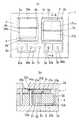
以下、本発明に係る加速度センサの実施形態について図面を用いて説明する。尚、以下の説明では、図1における上下を上下方向、センサチップ1の短手方向と平行な方向をx方向、センサチップ1の長手方向と平行な方向をy方向、x方向及びy方向に互いに直交する方向をz方向と定めるものとする。本実施形態は、図1,2に示すように、外形が矩形板状であるセンサチップ1と、センサチップ1の上面側に固定される上部固定板2aと、センサチップ1の下面側に固定される下部固定板2bとを備える。 Hereinafter, embodiments of an acceleration sensor according to the present invention will be described with reference to the drawings. In the following description, the vertical direction in FIG. 1 is the vertical direction, the direction parallel to the short direction of the
センサチップ1は、上下方向から見て矩形状の2つの枠部3a,3bが長手方向に並設されたフレーム部3と、枠部3a,3bの内周面に対して隙間を空けた状態で枠部3a,3b内に配置された直方体形状の重り部4,5と、枠部3a,3bの内周面と重り部4,5の側面とを連結してフレーム部3に対して重り部4,5を回動自在に支持する各1対のビーム部6a,6b及び7a,7bと、重り部4,5の上面に形成される可動電極4a,5aとを備える。 The
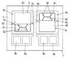
重り部4,5は、図1,3(b)に示すように、一面(下面)に開口する凹部41,51と、凹部41,51を除く充実部40,50とが一体に形成されている。凹部41,51は、開口面の法線方向(上下方向)から見て平面視四角形状に形成され、また、凹部41,51内を4分割する補強壁42,52が重り部4,5と一体に形成されている。 As shown in FIGS. 1 and 3 (b), the
ここで、本実施形態では、図4に示すように、平面視く字形の1対の補強壁42,52と各補強壁42,52の中央部が平坦な補強壁42’、52’で連結された構成、即ち、複数の補強壁42,52が凹部41,51の頂角と交わらない位置で内壁面と結合される構成を採用している。而して、凹部41,51の四隅において補強壁42,52と内壁面との成す角度が鈍角となるため、重り部4,5に凹部41,51を形成(エッチング)するのが容易となっている。 Here, in this embodiment, as shown in FIG. 4, a pair of reinforcing
1対のビーム部6a,6bは、重り部4の枠部3aと対向する側面のx方向における略中央部と枠部3aとを連結している。同様に、1対のビーム部7a,7bは、重り部5の枠部3bと対向する側面のx方向における略中央部と枠部3bとを連結している。而して、1対のビーム部6a,6bを結ぶ直線、並びに1対のビーム部7a,7bを結ぶ直線が回動軸となり、回動軸の回りに各重り部4,5が回動するようになっている。 The pair of
センサチップ1は、半導体の微細加工技術によりSOI(Silicon on Insulator)基板を加工して形成され、重り部4,5の上面を含む部位が可動電極4a,5aとなる。また、重り部4,5の上面及び下面には、重り部4,5が上部固定板2a及び下部固定板2bに直接衝突するのを防止するための突起部43a,43b,53a,53bが突設されている。 The
ここで、突起部43a,43b,53a,53bをシリコン又はシリコン酸化膜といったセンサチップの主材料により形成した場合には、突起部43a,43b,53a,53bを容易に製造することができる。尚、突起部43a,43b,53a,53bの表層をカーボン材料でコーティングしてもよい。この場合、突起部43a,43b,53a,53bの機械的強度が増し、上部固定板2a及び下部固定板2bとの衝突によって突起部43a,43b,53a,53bが破損するのを防止することができる。更に、カーボン材料としてカーボンナノチューブを採用すれば、コーティングの厚み寸法を小さくできるので、突起部43a,43b,53a,53bを所望の高さ寸法に容易に調整することができる。 Here, when the
上部固定板2aは、例えばガラス等の絶縁材料から形成され、その下面には、上下方向に沿ってセンサチップ1の重り部4(可動電極4a)と対向する位置に第1の固定電極20aと第2の固定電極20bとがx方向に並設されるととともに、上下方向に沿ってセンサチップ1の重り部5(可動電極5a)と対向する位置に第1の固定電極21aと第2の固定電極21bとがx方向に並設されている。また、上部固定板2aのx方向一端側には、5つの貫通孔22a〜22eがy方向に並べて貫設されている。更に、上部固定板2aの下面には、各固定電極20a,20b及び21a,21bと電気的に接続された複数の導電パターン(図示せず)が形成されている。 The upper fixed
一方、センサチップ1のx方向一端側には、フレーム部3から離間された計4つの電極部8a,8b,9a,9bが並設されている。これら4つの電極部8a,8b,9a,9bは、上面における略中央に金属膜から成る検出電極80a,80b,90a,90bがそれぞれ形成されるとともに、枠部3a,3bに臨む端部の上面に金属膜から成る圧接電極81a,81b,91a,91b(圧接電極91aのみ図示)がそれぞれ形成されている。尚、フレーム部3上面の電極部8b,9aの間には接地電極10が形成されている。そして、センサチップ1の上面に上部固定板2aが接合されると、上部固定板2aの下面に形成されている導電パターンと圧接電極81a,81b,91a,91bとが圧接接続されることで、各検出電極80a,80b,90a,90bが各固定電極20a,20b,21a,21bと電気的に接続されるとともに、上部固定板2aの貫通孔22a〜22dを介して各検出電極80a,80b,90a,90bが外部に露出する。尚、接地電極10も貫通孔22eを介して外部に露出する。 On the other hand, a total of four
尚、本実施形態では、図2に示すように、電極部8aと電極部8bとの間、電極部9aと電極部9bとの間、各電極部8a,8b,9a,9bとフレーム部3との間、各電極部8a,8b,9a,9bと各重り部4,5との間に各々隙間が設けられている。このように構成することで、各検出電極80a,80b,90a,90bが互いに電気的に絶縁されるので、各検出電極80a,80b,90a,90bの寄生容量や電極間のクロストークを低減し、高精度な静電容量の検出を行うことができる。 In this embodiment, as shown in FIG. 2, between the
下部固定板2bは、上部固定板2aと同様にガラス等の絶縁材料から形成され、その上面には上下方向に沿ってセンサチップ1の重り部4,5と対向する位置にそれぞれ付着防止膜23a,23bが形成されている。この付着防止膜23a,23bは、アルミニウム系合金等の固定電極20a,…と同じ材料で形成されており、回動した重り部4,5の下面が下部固定板2bに付着するのを防止している。このように、付着防止膜23a,23bを固定電極20a,…と同一材料で形成することにより、付着防止膜23a,23bを容易に形成することができる。このとき、付着防止膜23a,23bを固定電極20a,…と同時に形成すれば、重り部4,5と固定電極20a,…との間、及び重り部4,5と下部固定板2bとの間の距離の精度を高めることができる。 The
尚、付着防止膜23a,23bを半導体製造プロセスにより成膜した場合、付着防止膜23a,23bの表面に微小な凹凸が形成されるため、重り部4,5が下部固定板2bに付着するのをより好適に防止することができる。ここで、付着防止膜23a,23bをアルミニウム系合金により形成した場合、エッチング加工が容易になる。また、付着防止膜23a,23bの表面上に半導体製造プロセスとの整合性が良く、且つ加工がし易いポリイミド薄膜等の有機材料薄膜を形成することにより、付着防止膜23a,23bと重り部4,5との間の短絡を防止するようにしてもよい。 When the
ここで、本実施形態では、枠部3a、重り部4、ビーム部6a,6b、可動電極4a、第1及び第2の固定電極20a,20b、検出電極80a,80bと、枠部3b、重り部5、ビーム部7a,7b、可動電極5a、第1及び第2の固定電極21a,21b、検出電極90a,90bとで各々センサ部が構成され、重り部4,5の向き(充実部40,50と凹部41,51の配置)を180度反転させた状態で2つのセンサ部が一体に形成されている。 Here, in this embodiment, the
次に、本実施形態の検出動作について説明する。先ず、一方の重り部4にx方向の加速度が印加された場合を考える。x方向に加速度が印加されると、重り部4が回動軸の回りに回動して可動電極4aと第1の固定電極20a並びに第2の固定電極20bとの間の距離が変化し、その結果、可動電極4aと各固定電極20a,20bとの間の静電容量C1,C2も変化する。ここで、x方向の加速度が印加されていないときの可動電極4aと各固定電極20a,20bとの間の静電容量をC0とし、加速度の印加によって生じる静電容量の変化分をΔCとすれば、x方向の加速度が印加されたときの静電容量C1,C2は、
C1=C0−ΔC …(1)
C2=C0+ΔC …(2)
と表すことができる。Next, the detection operation of this embodiment will be described. First, consider a case where an acceleration in the x direction is applied to one
C1 = C0−ΔC (1)
C2 = C0 + ΔC (2)
It can be expressed as.
同様に、他方の重り部5にx方向の加速度が印加された場合、可動電極5aと各固定電極21a,21bとの間の静電容量C3,C4は、
C3=C0−ΔC …(3)
C4=C0+ΔC …(4)
と表すことができる。Similarly, when an acceleration in the x direction is applied to the
C3 = C0−ΔC (3)
C4 = C0 + ΔC (4)
It can be expressed as.
ここで、静電容量C1〜C4の値は、検出電極80a,80b及び90a,90bから取出す電圧信号を演算処理することで検出することができる。そして、一方のセンサ部から得られる静電容量C1,C2の差分値CA(=C1−C2)と、他方のセンサ部から得られる静電容量C3,C4の差分値CB(=C3−C4)との和(±4ΔC)を算出すれば、この差分値CA,CBの和に基づいてx方向に印加された加速度の向きと大きさを演算することができる。 Here, the values of the capacitances C1 to C4 can be detected by performing arithmetic processing on voltage signals taken from the
次に、一方の重り部4にz方向の加速度が印加された場合を考える。z方向に加速度が印加されると重り部4が回動軸の回りに回動して可動電極4aと第1の固定電極20a並びに第2の固定電極20bとの間の距離が変化し、その結果、可動電極4aと各固定電極20a,20bとの間の静電容量C1,C2も変化する。ここで、z方向の加速度が印加されていないときの可動電極4aと各固定電極20a,20bとの間の静電容量をC0とし、加速度の印加によって生じる静電容量の変化分をΔCとすれば、z方向の加速度が印加されたときの静電容量C1,C2は、
C1=C0+ΔC …(5)
C2=C0−ΔC …(6)
と表すことができる。Next, consider a case where an acceleration in the z direction is applied to one
C1 = C0 + ΔC (5)
C2 = C0−ΔC (6)
It can be expressed as.
同様に、他方の重り部5にz方向の加速度が印加された場合、可動電極5aと各固定電極21,21bとの間の静電容量C3,C4は、
C3=C0−ΔC …(7)
C4=C0+ΔC …(8)
と表すことができる。Similarly, when acceleration in the z direction is applied to the
C3 = C0−ΔC (7)
C4 = C0 + ΔC (8)
It can be expressed as.
そして、一方のセンサ部から得られる静電容量C1,C2の差分値CA(=C1−C2)と、他方のセンサ部から得られる静電容量C3,C4の差分値CB(=C3−C4)との差(±4ΔC)を算出すれば、この差分値CA,CBの差に基づいてz方向に印加された加速度の向きと大きさを演算することができる。尚、差分値CA,CBの和と差とに基づいてx方向及びz方向の加速度の向きと大きさを求める演算処理については従来周知であるので、ここでは詳細な説明を省略する。 Then, the difference value CA (= C1-C2) between the capacitances C1, C2 obtained from one sensor unit and the difference value CB (= C3-C4) between the capacitances C3, C4 obtained from the other sensor unit. Is calculated (± 4ΔC), the direction and magnitude of the acceleration applied in the z direction can be calculated based on the difference between the difference values CA and CB. Note that calculation processing for obtaining the direction and magnitude of the acceleration in the x direction and the z direction based on the sum and difference of the difference values CA and CB is well known in the art, and detailed description thereof is omitted here.
ところで、前述のように、加速度センサの検出感度を高めるべく可動電極4a,5aの面積を大きくする場合、重り部4,5の重心位置から回動軸に下ろした垂線と可動電極4a,5aの表面とが成す角度を略45度に維持するために、重り部4,5の厚み寸法を大きくする、或いは重り部4,5のビーム部6a,6b,7a,7bの直下を刳り貫いて軽量化する方法は望ましくない。そこで、本実施形態では、図1に示すように、ビーム部6a,6b,7a,7b(同図ではビーム部6bのみ図示)を重り部4,5の長手方向における略中央から凹部41,51側(右側)にずらして配置することで、重り部4,5の重心位置から回動軸に下ろした垂線と可動電極4a,5aの表面とが成す角度θを略45度となるようにしている。而して、ビーム部6a,6b,7a,7bをずらして配置するだけで角度θを略45度に維持することができるため、重り部4,5の厚み寸法を大きくする、或いは重り部4,5を軽量化することなく検出感度を向上させることができる。 By the way, as described above, when the area of the
尚、本実施形態では、以下の手順を踏むことで加速度センサの動作確認を行うことができる。即ち、第1の固定電極20a又は第2の固定電極20bと可動電極4aとの間、若しくは第1の固定電極21a又は第2の固定電極21bと可動電極5aとの間に吸引力を発生させることで、重り部4,5を回動させる。そして、重り部4,5の回動に伴って生じる各固定電極20a,…と重り部4,5との間の静電容量の変化を検出することで、加速度センサが正常に動作しているか否かを確認することができる。尚、付着防止膜23a,23bと可動電極4a,5aとの間に吸引力を発生させることで同様の動作確認を行ってもよい。 In the present embodiment, the operation of the acceleration sensor can be confirmed by following the following procedure. That is, an attractive force is generated between the first
また、本実施形態では、x方向とz方向の2方向の加速度を検出する加速度センサを例示したが、上述のセンサ部の1つをxy平面内で90度回転対称に配置すれば、y方向を加えた3方向の加速度を検出する加速度センサを実現することができる。また、3つのセンサ部を同一チップに配置し、2つのセンサ部を、それぞれ残りの1つのセンサ部に対してxy平面において90度及び180度回転対称に配置しても、上記と同様に3方向の加速度を検出する加速度センサを実現することができる。 In the present embodiment, an acceleration sensor that detects acceleration in two directions, the x direction and the z direction, is illustrated. However, if one of the above-described sensor units is arranged 90 degrees rotationally symmetrical in the xy plane, the y direction Thus, it is possible to realize an acceleration sensor that detects acceleration in three directions with the addition of. Further, even if three sensor units are arranged on the same chip and two sensor units are arranged symmetrically by 90 degrees and 180 degrees on the xy plane with respect to the remaining one sensor part, 3 An acceleration sensor that detects the acceleration in the direction can be realized.
20a,21a 第1の固定電極
20b,21b 第2の固定電極
4,5 重り部
40,50 充実部
41,51 凹部
4a,5a 可動電極
6a,6b ビーム部
7a,7b ビーム部
20a, 21a 1st fixed
Claims (19)
Translated fromJapanesePriority Applications (8)
| Application Number | Priority Date | Filing Date | Title |
|---|---|---|---|
| JP2009266581AJP5716149B2 (en) | 2009-11-24 | 2009-11-24 | Acceleration sensor |
| US13/511,178US9261530B2 (en) | 2009-11-24 | 2010-11-23 | Acceleration sensor |
| PCT/IB2010/002975WO2011064642A2 (en) | 2009-11-24 | 2010-11-23 | Acceleration sensor |
| CN201080052810.1ACN102667497B (en) | 2009-11-24 | 2010-11-23 | Acceleration sensor |
| EP10832714.9AEP2506018A4 (en) | 2009-11-24 | 2010-11-23 | ACCELERATION SENSOR |
| US14/718,493US9244094B2 (en) | 2009-11-24 | 2015-05-21 | Acceleration sensor |
| US14/874,845US9702895B2 (en) | 2009-11-24 | 2015-10-05 | Acceleration sensor |
| US15/617,777US10126322B2 (en) | 2009-11-24 | 2017-06-08 | Acceleration sensor |
Applications Claiming Priority (1)
| Application Number | Priority Date | Filing Date | Title |
|---|---|---|---|
| JP2009266581AJP5716149B2 (en) | 2009-11-24 | 2009-11-24 | Acceleration sensor |
Publications (2)
| Publication Number | Publication Date |
|---|---|
| JP2011112388Atrue JP2011112388A (en) | 2011-06-09 |
| JP5716149B2 JP5716149B2 (en) | 2015-05-13 |
Family
ID=44234848
Family Applications (1)
| Application Number | Title | Priority Date | Filing Date |
|---|---|---|---|
| JP2009266581AActiveJP5716149B2 (en) | 2009-11-24 | 2009-11-24 | Acceleration sensor |
Country Status (1)
| Country | Link |
|---|---|
| JP (1) | JP5716149B2 (en) |
Cited By (4)
| Publication number | Priority date | Publication date | Assignee | Title |
|---|---|---|---|---|
| WO2017061640A1 (en)* | 2015-10-06 | 2017-04-13 | 주식회사 스탠딩에그 | Mems device, mems package comprising same and user terminal |
| CN113933540A (en)* | 2021-11-19 | 2022-01-14 | 中国工程物理研究院电子工程研究所 | Electromechanical coupling capacitance type acceleration sensor |
| JP2023008854A (en)* | 2021-07-05 | 2023-01-19 | 株式会社村田製作所 | Accelerometer having two seesaws |
| CN116233287A (en)* | 2023-01-13 | 2023-06-06 | 上海艾为电子技术股份有限公司 | A state detection device and method |
Citations (11)
| Publication number | Priority date | Publication date | Assignee | Title |
|---|---|---|---|---|
| JPH0843426A (en)* | 1994-06-29 | 1996-02-16 | Texas Instr Inc <Ti> | Micro-mechanical type digital accelerometer |
| US5659195A (en)* | 1995-06-08 | 1997-08-19 | The Regents Of The University Of California | CMOS integrated microsensor with a precision measurement circuit |
| JP2000019198A (en)* | 1998-06-29 | 2000-01-21 | Zexel Corp | Acceleration sensor |
| JP2005076756A (en)* | 2003-09-01 | 2005-03-24 | Nippon Parkerizing Co Ltd | Carbon nanotube sliding member and manufacturing method thereof |
| WO2006009194A1 (en)* | 2004-07-21 | 2006-01-26 | Hokuriku Electric Industry Co., Ltd. | Semiconductor sensor |
| JP2006133245A (en)* | 2006-02-16 | 2006-05-25 | Mitsubishi Electric Corp | Capacitive acceleration sensor |
| JP2006172662A (en)* | 2004-12-17 | 2006-06-29 | Fujitsu Ltd | Magnetic recording medium and magnetic recording apparatus |
| JP2006519387A (en)* | 2003-03-05 | 2006-08-24 | ヴェーテーイー テクノロジーズ オサケユキチュア | Capacitive acceleration sensor |
| JP2007298405A (en)* | 2006-04-28 | 2007-11-15 | Matsushita Electric Works Ltd | Electrostatic capacity type sensor |
| JP2008544243A (en)* | 2005-06-17 | 2008-12-04 | ヴェーテーイー テクノロジーズ オサケユキチュア | Method for manufacturing capacitive acceleration sensor and capacitive acceleration sensor |
| WO2009020716A1 (en)* | 2007-08-03 | 2009-02-12 | Freescale Semiconductor Inc. | Symmetrical differential capacitive sensor and method of making same |
- 2009
- 2009-11-24JPJP2009266581Apatent/JP5716149B2/enactiveActive
Patent Citations (11)
| Publication number | Priority date | Publication date | Assignee | Title |
|---|---|---|---|---|
| JPH0843426A (en)* | 1994-06-29 | 1996-02-16 | Texas Instr Inc <Ti> | Micro-mechanical type digital accelerometer |
| US5659195A (en)* | 1995-06-08 | 1997-08-19 | The Regents Of The University Of California | CMOS integrated microsensor with a precision measurement circuit |
| JP2000019198A (en)* | 1998-06-29 | 2000-01-21 | Zexel Corp | Acceleration sensor |
| JP2006519387A (en)* | 2003-03-05 | 2006-08-24 | ヴェーテーイー テクノロジーズ オサケユキチュア | Capacitive acceleration sensor |
| JP2005076756A (en)* | 2003-09-01 | 2005-03-24 | Nippon Parkerizing Co Ltd | Carbon nanotube sliding member and manufacturing method thereof |
| WO2006009194A1 (en)* | 2004-07-21 | 2006-01-26 | Hokuriku Electric Industry Co., Ltd. | Semiconductor sensor |
| JP2006172662A (en)* | 2004-12-17 | 2006-06-29 | Fujitsu Ltd | Magnetic recording medium and magnetic recording apparatus |
| JP2008544243A (en)* | 2005-06-17 | 2008-12-04 | ヴェーテーイー テクノロジーズ オサケユキチュア | Method for manufacturing capacitive acceleration sensor and capacitive acceleration sensor |
| JP2006133245A (en)* | 2006-02-16 | 2006-05-25 | Mitsubishi Electric Corp | Capacitive acceleration sensor |
| JP2007298405A (en)* | 2006-04-28 | 2007-11-15 | Matsushita Electric Works Ltd | Electrostatic capacity type sensor |
| WO2009020716A1 (en)* | 2007-08-03 | 2009-02-12 | Freescale Semiconductor Inc. | Symmetrical differential capacitive sensor and method of making same |
Cited By (6)
| Publication number | Priority date | Publication date | Assignee | Title |
|---|---|---|---|---|
| WO2017061640A1 (en)* | 2015-10-06 | 2017-04-13 | 주식회사 스탠딩에그 | Mems device, mems package comprising same and user terminal |
| JP2023008854A (en)* | 2021-07-05 | 2023-01-19 | 株式会社村田製作所 | Accelerometer having two seesaws |
| JP7380761B2 (en) | 2021-07-05 | 2023-11-15 | 株式会社村田製作所 | Accelerometer with two seesaws |
| CN113933540A (en)* | 2021-11-19 | 2022-01-14 | 中国工程物理研究院电子工程研究所 | Electromechanical coupling capacitance type acceleration sensor |
| CN113933540B (en)* | 2021-11-19 | 2023-08-04 | 中国工程物理研究院电子工程研究所 | Electromechanical coupling capacitive acceleration sensor |
| CN116233287A (en)* | 2023-01-13 | 2023-06-06 | 上海艾为电子技术股份有限公司 | A state detection device and method |
Also Published As
| Publication number | Publication date |
|---|---|
| JP5716149B2 (en) | 2015-05-13 |
Similar Documents
| Publication | Publication Date | Title |
|---|---|---|
| US10126322B2 (en) | Acceleration sensor | |
| JP5789737B2 (en) | Acceleration sensor | |
| JP5716149B2 (en) | Acceleration sensor | |
| CN102124352B (en) | Acceleration sensor and structure | |
| JP2013181884A (en) | Electrostatic capacitance sensor | |
| JP5426906B2 (en) | Acceleration sensor | |
| JP4965546B2 (en) | Acceleration sensor | |
| JP4965547B2 (en) | Acceleration sensor | |
| JP2011112392A (en) | Acceleration sensor | |
| JP2011112390A (en) | Acceleration sensor | |
| JP2010210420A (en) | Acceleration sensor | |
| JP2013231616A (en) | Acceleration sensor | |
| JP2011112389A (en) | Acceleration sensor | |
| JP2012220376A (en) | Acceleration sensor | |
| JP2010210430A (en) | Acceleration sensor | |
| JP2010210422A (en) | Acceleration sensor | |
| JP2010210418A (en) | Acceleration sensor | |
| JP2013231617A (en) | Acceleration sensor | |
| JP2010210426A (en) | Acceleration sensor and method for manufacturing the same | |
| JP2013186061A (en) | Capacitive sensor | |
| JP2010210417A (en) | Acceleration sensor | |
| JP2013127388A (en) | Capacitance type sensor | |
| JP2012008022A (en) | Acceleration sensor | |
| JP2012008036A (en) | Capacitance type sensor | |
| JP2012047530A (en) | Electrostatic capacitance type sensor |
Legal Events
| Date | Code | Title | Description |
|---|---|---|---|
| A711 | Notification of change in applicant | Free format text:JAPANESE INTERMEDIATE CODE: A712 Effective date:20120118 | |
| A621 | Written request for application examination | Free format text:JAPANESE INTERMEDIATE CODE: A621 Effective date:20121004 | |
| A131 | Notification of reasons for refusal | Free format text:JAPANESE INTERMEDIATE CODE: A131 Effective date:20130730 | |
| A521 | Written amendment | Free format text:JAPANESE INTERMEDIATE CODE: A523 Effective date:20130930 | |
| A02 | Decision of refusal | Free format text:JAPANESE INTERMEDIATE CODE: A02 Effective date:20140513 | |
| A521 | Written amendment | Free format text:JAPANESE INTERMEDIATE CODE: A523 Effective date:20140811 | |
| A911 | Transfer of reconsideration by examiner before appeal (zenchi) | Free format text:JAPANESE INTERMEDIATE CODE: A911 Effective date:20140819 | |
| TRDD | Decision of grant or rejection written | ||
| A01 | Written decision to grant a patent or to grant a registration (utility model) | Free format text:JAPANESE INTERMEDIATE CODE: A01 Effective date:20141007 | |
| A711 | Notification of change in applicant | Free format text:JAPANESE INTERMEDIATE CODE: A711 Effective date:20141009 | |
| A61 | First payment of annual fees (during grant procedure) | Free format text:JAPANESE INTERMEDIATE CODE: A61 Effective date:20141030 | |
| R151 | Written notification of patent or utility model registration | Ref document number:5716149 Country of ref document:JP Free format text:JAPANESE INTERMEDIATE CODE: R151 |