JP2011108349A - Semiconductor memory device - Google Patents
Semiconductor memory deviceDownload PDFInfo
- Publication number
- JP2011108349A JP2011108349AJP2009265450AJP2009265450AJP2011108349AJP 2011108349 AJP2011108349 AJP 2011108349AJP 2009265450 AJP2009265450 AJP 2009265450AJP 2009265450 AJP2009265450 AJP 2009265450AJP 2011108349 AJP2011108349 AJP 2011108349A
- Authority
- JP
- Japan
- Prior art keywords
- circuit
- clock
- reference voltage
- planes
- selection
- Prior art date
- Legal status (The legal status is an assumption and is not a legal conclusion. Google has not performed a legal analysis and makes no representation as to the accuracy of the status listed.)
- Withdrawn
Links
Images


Landscapes
- Read Only Memory (AREA)
Abstract
Translated fromJapaneseDescription
Translated fromJapaneseこの発明は、半導体記憶装置に関し、例えば、NAND型フラッシュメモリ等に適用されるものである。 The present invention relates to a semiconductor memory device, and is applied to, for example, a NAND flash memory.
例えば、NAND型フラッシュメモリ等の半導体記憶装置において、複数のプレーン(マルチプレーン)で構成されているものがある。この構成の場合、選択されるプレーン数により、昇圧回路から見える負荷容量が変わってくる。この場合、昇圧回路の能力を、最大プレーンの負荷容量がある時間までに昇圧できるように合わせると、単プレーンの負荷容量を昇圧するには過剰となり、昇圧回路の回路面積も大きくなってしまう。 For example, some semiconductor storage devices such as NAND flash memory are configured with a plurality of planes (multiplanes). In the case of this configuration, the load capacity seen from the booster circuit varies depending on the number of selected planes. In this case, if the capacity of the booster circuit is adjusted so that the load capacity of the maximum plane can be boosted by a certain time, it is excessive to boost the load capacity of the single plane, and the circuit area of the booster circuit also increases.
一方、昇圧回路の能力を、単プレーン(シングルプレーン)の負荷容量がある時間までに昇圧できるように合わせると、複数プレーンを選択したときの負荷容量を昇圧するには、能力不足となり、昇圧時間を延ばす必要がある。 On the other hand, when the capacity of the booster circuit is adjusted so that the load capacity of a single plane (single plane) can be boosted by a certain time, the capacity is insufficient to boost the load capacity when multiple planes are selected, and the boost time Need to be extended.
上記のように、従来の半導体記憶装置は、昇圧時間の低減化および微細化に対して不利であるという傾向がある。 As described above, the conventional semiconductor memory device tends to be disadvantageous for the reduction and miniaturization of the boost time.
この発明は、昇圧時間の低減化および微細化に対して有利な半導体記憶装置を提供する。 The present invention provides a semiconductor memory device that is advantageous for reducing the step-up time and miniaturizing it.
この発明の一態様に係る半導体記憶装置は、複数のメモリセルをそれぞれ有するN個(Nは2以上の整数)のプレーンを備えるメモリセルアレイと、第1基準電圧および前記第1基準電圧よりも高い第2基準電圧を発生させる基準電圧生成回路と、前記基準電圧生成回路から与えられる前記第1または第2基準電圧を昇圧した昇圧電圧を前記プレーンに供給する昇圧回路と、(N−1)個以下の前記プレーンを選択する場合は前記第1基準電圧を前記昇圧回路に与え、N個の前記プレーンを選択する場合は前記第2基準電圧を前記昇圧回路に与える昇圧能力制御回路とを具備する。 A semiconductor memory device according to an aspect of the present invention includes a memory cell array including N (N is an integer of 2 or more) planes each having a plurality of memory cells, a first reference voltage, and higher than the first reference voltage A reference voltage generation circuit for generating a second reference voltage; a booster circuit for supplying a boosted voltage obtained by boosting the first or second reference voltage supplied from the reference voltage generation circuit to the plane; and (N−1) pieces. A boosting capability control circuit that applies the first reference voltage to the booster circuit when selecting the following planes, and applies the second reference voltage to the booster circuit when selecting N planes; .
この発明によれば、微細化および昇圧時間の低減化に対して有利な半導体記憶装置が得られる。 According to the present invention, it is possible to obtain a semiconductor memory device that is advantageous for miniaturization and reduction of boost time.
以下、この発明の実施形態について図面を参照して説明する。尚、この説明においては、全図にわたり共通の部分には共通の参照符号を付す。 Embodiments of the present invention will be described below with reference to the drawings. In this description, common parts are denoted by common reference symbols throughout the drawings.
[第1の実施形態]
図1乃至図13を用いて、この発明の第1の実施形態に係る半導体記憶装置およびその昇圧動作を説明する。[First Embodiment]
A semiconductor memory device and its boosting operation according to the first embodiment of the present invention will be described with reference to FIGS.
<1.構成例>
1−1.全体構成例
図1を用い、第1の実施形態に係る半導体記憶装置の全体構成例について説明する。<1. Configuration example>
1-1. Overall configuration example
An example of the overall configuration of the semiconductor memory device according to the first embodiment will be described with reference to FIG.
図示するように、第1の実施形態に係る半導体集積回路装置は、メモリセルアレイ11、ビット線制御回路12、カラムデコーダ13、データ入出力バッファ14、データ入出力端子15、ワード線制御回路16、制御回路17、制御信号入力端子18、電源電圧発生回路19、およびクロック発生回路20を備える。 As illustrated, the semiconductor integrated circuit device according to the first embodiment includes a
メモリセルアレイ11は、複数のプレーン(Plane)を備える。本例の場合、メモリセルアレイ11は、4つのプレーン(Plane<0>, Plane<1>, Plane<2>, Plane<3>)を備える4つの複数プレーン構成である。プレーンのそれぞれは、ワード線とビット線との交差位置にマトリクス状に配置される複数のメモリセル(図示せず)を有する複数のブロック(Block 0 〜 Block n)を備える。メモリセルアレイ11には、ワード線を制御するワード線制御回路16、ビット線を制御するビット制御回路12、制御回路17、および電源電圧発生回路19が電気的に接続される。 The
ビット線制御回路12は、ビット線を介してメモリセルアレイ11中のメモリセルのデータを読み出し、ビット線を介してメモリセルアレイ11中のメモリセルの状態を検出する。また、ビット線制御回路12は、ビット線を介してメモリセルアレイ11中のメモリセルに書き込み制御電圧を印加してメモリセルに書き込みを行う。ビット線制御回路12には、カラムデコーダ13、データ入出力バッファ14、制御回路17が電気的に接続されている。 The bit
ビット線制御回路12内にはセンスアンプ(S/A)やデータ記憶回路等(図示せず)が設けられ、このデータ記憶回路は、カラムデコーダ13によって選択される。データ記憶回路に読み出されたメモリセルのデータは、データ入出力バッファ14を介してデータ入出力端子15から外部へ出力される。データ入出力端子15は、例えば、NAND型フラッシュメモリ外部のホスト機器等に接続される。 A sense amplifier (S / A), a data storage circuit, etc. (not shown) are provided in the bit
ホスト機器は、例えば、マイクロコンピュータ等であって、データ入出力端子15から出力されたデータを受ける。さらに、ホスト機器は、NAND型フラッシュメモリの動作を制御する各種コマンドCOM、アドレスADD、及びデータDTをデータ入出力端子15に出力する。ホスト機器からデータ入出力端子15に入力された書き込みデータDTは、データ入出力バッファ14を介して、カラムデコーダ13によって選択された上記データ記憶回路(図示せず)に供給される。一方、コマンドCOM及びアドレスADDは、制御回路17に供給される。 The host device is, for example, a microcomputer and receives data output from the data input /
ワード線制御回路16は、メモリセルアレイ11中のワード線を選択し、選択されたワード線に電源電圧発生回路19から与えられる読み出し、書き込みあるいは消去に必要な電圧を印加する。 The word
制御回路17は、上記メモリセルアレイ11、ビット線制御回路12、カラムデコーダ13、データ入出力バッファ14、ワード線制御回路16、および電源電圧発生回路19に電気的に接続される。制御回路17は、接続された上記構成回路を制御する。制御回路17は、制御信号入力端子18に接続され、外部のホスト機器から制御信号入力端子18を介して入力されるALE(アドレス・ラッチ・イネーブル)信号等の制御信号によって制御される。また、制御回路17は、電源電圧発生回路19に後述する制御信号を出力し、電源電圧発生回路19を制御する。 The
電源電圧発生回路19は、制御回路17の制御に従い、書き込み、読み出し、消去等の各動作において、メモリセルアレイ11、ワード線制御回路16等に必要な電源電圧を与える。詳細については、後述する。 The power supply
クロック発生回路20は、本例の場合、少なくとも2つの第1,第2クロック発生回路20−1、20−2を備える。第1,第2クロックCLKA,CLKBは電源電圧発生回路19に供給され、第2クロックCLKBは制御回路17に供給され、それぞれ必要な動作の際に用いられる。 In this example, the
上記のように、第2クロック発生回路20−2が発生する第2クロックCLKBは、電源電圧発生回路19および制御回路17により共有するように構成されている。すなわち、電源電圧発生回路19に供給される第2クロックCLKBとして、従来から制御回路17に供給されていたクロックを流用する。そのため、第2クロックCLKBを発生させるための新たなクロック発生回路を配置する必要がない点で、製造コストの低減に対して有利である。尚、制御回路17に供給されるクロックとは別に、新たなクロック発生回路を設けても良い。 As described above, the second clock CLKB generated by the second clock generation circuit 20-2 is configured to be shared by the power supply
ここで、上記ワード線制御回路16、ビット線制御回路12、カラムデコーダ13、制御回路17、電源電圧発生回路19は、書き込み回路、読み出し回路、および消去回路を構成している。 Here, the word
1−2.ブロックの構成例
次に、図2を用い、第1の実施形態に係るブロック(Block)の構成例について説明する。ここでは、1つのブロックBLOCKを例に挙げて説明する。また、このブロックBLOCK中のメモリセルトランジスタMTは、一括して消去される。即ち、ブロックは消去単位である。1-2. Block Configuration Example Next, a configuration example of a block (Block) according to the first embodiment will be described with reference to FIG. Here, one block BLOCK will be described as an example. Further, the memory cell transistors MT in the block BLOCK are erased collectively. That is, a block is an erase unit.
図示するように、ブロックBLOCKは、ワード線方向(WL方向)に配置された複数のメモリセル列(メモリセルユニット)MUから構成される。メモリセル列MUは、電流経路が直列接続される64個のメモリセルトランジスタMTおよび2個のダミーセルDMTからなるNANDストリングと、NANDストリングの一端に接続される選択ランジスタS1と、NANDストリングの他端に接続される選択トランジスタS2とから構成される。尚、本例では、NANDストリングは、64個のメモリセルMTから構成されるが、2つ以上のメモリセルから構成されていればよく、特に、この個数に限定されるというものではない。 As shown in the figure, the block BLOCK is composed of a plurality of memory cell columns (memory cell units) MU arranged in the word line direction (WL direction). The memory cell column MU includes a NAND string composed of 64 memory cell transistors MT and two dummy cells DMT whose current paths are connected in series, a selection transistor S1 connected to one end of the NAND string, and the other end of the NAND string. And a selection transistor S2 connected to the. In this example, the NAND string is composed of 64 memory cells MT. However, the NAND string only needs to be composed of two or more memory cells, and is not particularly limited to this number.
選択トランジスタS2の電流経路の他端はビット線BLに接続され、選択トランジスタS1の電流経路の他端はソース線SLに接続される。 The other end of the current path of the selection transistor S2 is connected to the bit line BL, and the other end of the current path of the selection transistor S1 is connected to the source line SL.
ワード線WL0〜WL63およびダミーワード線DWLは、WL方向に延び、WL方向の複数のメモリセルトランジスタMTおよびダミーセルDMTに共通に接続される。セレクトゲート線SGDは、WL方向に延び、WL方向の複数の選択トランジスタS2に共通に接続される。セレクトゲート線SGSも、WL方向に延び、WL方向の複数の選択トランジスタS1に共通に接続される。 Word lines WL0 to WL63 and dummy word line DWL extend in the WL direction and are commonly connected to a plurality of memory cell transistors MT and dummy cells DMT in the WL direction. The select gate line SGD extends in the WL direction and is commonly connected to a plurality of select transistors S2 in the WL direction. The select gate line SGS also extends in the WL direction and is commonly connected to a plurality of select transistors S1 in the WL direction.
ワード線WL0〜WL63ごとに、ページ(Page)と称する単位を構成する。例えば、図中の破線で囲って示すように、ワード線WL0には、1ページ(Page0)が割り当てられている。このページごとに読み出し動作、書き込み動作が行われるため、ページは読み出し単位であり、書き込み単位である。尚、1つのメモリセルに複数ビットのデータを保持可能な多値メモリセルの場合は、1つのワード線に複数ページが割り当てられる。 A unit called a page is configured for each of the word lines WL0 to WL63. For example, one page (Page 0) is allocated to the word line WL0 as indicated by being surrounded by a broken line in the figure. Since a read operation and a write operation are performed for each page, the page is a read unit and a write unit. In the case of a multilevel memory cell that can hold a plurality of bits of data in one memory cell, a plurality of pages are assigned to one word line.
メモリセルMTは、ビット線BLとワード線WLとの交差位置にそれぞれ設けられ、半導体基板上に順次、トンネル絶縁膜、電荷蓄積層としての浮遊電極FG、ゲート間絶縁膜、及び制御電極CGが設けられた積層構造である。メモリセルMTの電流経路であるソース/ドレインは、隣接するメモリセルMTのソース/ドレインに直列接続されている。電流経路の一端は選択トランジスタS2を介してビット線BLに接続され、電流経路の他端は選択トランジスタS1を介してソース線SLに接続される。また、メモリセルMTのそれぞれは、積層構造の側壁上に沿って設けられたスペーサ、及び上記積層構造を挟むように半導体基板(Si基板(Si−sub)またはPウェル)中に設けられたソース/ドレインを備えている。 The memory cell MT is provided at each intersection of the bit line BL and the word line WL, and a tunnel insulating film, a floating electrode FG as a charge storage layer, an inter-gate insulating film, and a control electrode CG are sequentially formed on the semiconductor substrate. It is the laminated structure provided. The source / drain which is the current path of the memory cell MT is connected in series to the source / drain of the adjacent memory cell MT. One end of the current path is connected to the bit line BL via the selection transistor S2, and the other end of the current path is connected to the source line SL via the selection transistor S1. Each of the memory cells MT includes a spacer provided along the side wall of the stacked structure, and a source provided in a semiconductor substrate (Si substrate (Si-sub) or P well) so as to sandwich the stacked structure. / Has a drain.
選択トランジスタS1、S2は、ゲート絶縁膜、ゲート間絶縁膜、ゲート電極を備えている。選択トランジスタS1、S2のゲート間絶縁膜は、その中央が分離され、その上下層が電気的に接続するように設けられている。選択トランジスタS1、S2は、同様に、ゲート電極の側壁上に沿って設けられたスペーサ、及びゲート電極を挟むように半導体基板中に設けられたソース/ドレインを備えている。 The selection transistors S1 and S2 include a gate insulating film, an inter-gate insulating film, and a gate electrode. The intergate insulating films of the select transistors S1 and S2 are provided so that the centers thereof are separated and the upper and lower layers thereof are electrically connected. Similarly, the select transistors S1 and S2 include a spacer provided along the side wall of the gate electrode and a source / drain provided in the semiconductor substrate so as to sandwich the gate electrode.
1−2−1.ROMセル回路
次に、図3を用い、第1の実施形態に係るROMセル回路の構成例について説明する。
図示するように、ROMセル回路は、後述する昇圧動作のために用いられる信号Bを、例えば、パワーオン時等に、ROMセル(MT)から読出し、ラッチ回路DEFにラッチし、電源電圧発生回路19へ供給するためのものである。ROMセル回路は、ROMセル(MT)、センスアンプS/A、およびラッチ回路DEFにより構成される。
ROMセルは、上記ブロックと同様の構成であるROM fuse Blockに配置される、メモリセルトランジスタ(MT)である。ROMセルには、例えば、NAND型フラッシュメモリに必要な管理データ等が不揮発に記憶されており、これがデータオン時に読み出される。
センスアンプS/Aは、ビット線制御回路12に配置され、ROMセル(MT)に記憶された管理データ等を読み出す。
ラッチ回路DEFは、制御回路17に配置され、センスアンプS/Aから読み出されたデータ、またはROMセル(MT)に書込むデータを一時的に記憶する。ラッチ回路DEFは、リセット信号RSTが入力されるまで、供給されるクロックCLKのタイミングで信号Bを出力する。
尚、本例のように、信号Bは、ROMセルに記憶されるロムデータであるため、必要に応じて、信号Bの値を書き換えることにより、昇圧条件を変更することが可能である。例えば、テストモード時において、複数プレーンを同時に選択して駆動する場合に、信号Bの値を書き換えることが可能である。さらに、信号Bの記憶は、本例のROMセル(MT)に限らず、例えば、ヒューズ等であっても良い。1-2-1. ROM cell circuit
Next, a configuration example of the ROM cell circuit according to the first embodiment will be described with reference to FIG.
As shown in the figure, the ROM cell circuit reads a signal B used for a boosting operation, which will be described later, from the ROM cell (MT) at the time of power-on, for example, and latches it in the latch circuit DEF. 19 to supply. The ROM cell circuit includes a ROM cell (MT), a sense amplifier S / A, and a latch circuit DEF.
The ROM cell is a memory cell transistor (MT) arranged in a ROM fuse block having the same configuration as the above block. In the ROM cell, for example, management data necessary for a NAND flash memory is stored in a nonvolatile manner, and this is read when data is turned on.
The sense amplifier S / A is arranged in the bit
The latch circuit DEF is disposed in the
Since the signal B is ROM data stored in the ROM cell as in this example, the boosting condition can be changed by rewriting the value of the signal B as necessary. For example, the value of the signal B can be rewritten when a plurality of planes are simultaneously selected and driven in the test mode. Furthermore, the storage of the signal B is not limited to the ROM cell (MT) of this example, and may be a fuse, for example.
1−3.電源電圧発生回路の構成例
次に、図4を用い、第1の実施形態に係る電源電圧発生回路19の構成例について説明する。尚、本例では、4個のプレーン(Plane<0>, Plane<1>, Plane<2>, Plane<3>)を備えるメモリセルアレイ11を一例に挙げるが、これに限られず、N個(Nは2以上の整数)のプレーンを備えるメモリセルアレイであれば同様に適用できる。また、4個のプレーンのそれぞれには、ブロックを選択するためのブロックデコーダ(Block decoder <0>, Block decoder <1>, Block decoder <2>, Block decoder <3>)が配置される。1-3. Configuration example of power supply voltage generation circuit
Next, a configuration example of the power supply
図示するように、電源電圧発生回路19は、基準電圧生成回路31,昇圧回路32,昇圧能力制御回路33を備える。 As illustrated, the power supply
基準電圧生成回路31は、第1基準電圧(VI0)および第1基準電圧よりも高い第2基準電圧(VI1)を発生させる。発生された上記第1,第2基準電圧は、昇圧能力制御回路33の制御により、基準電圧PMPDRREFとして、昇圧回路32に与えられる。
昇圧回路32は、基準電圧生成回路31から与えられる上記第1または第2基準電圧(VI0,VI1)としての基準電圧PMPDRREFを昇圧した昇圧電圧(VPPOUT,VREADOUT,VRDOUT等)を各プレーンに供給する。換言すると、昇圧回路32は、与えられた基準電圧PMPDRREFを用い、メモリセルアレイ11の所動作に対応する所定の電圧(VPPOUT,VREADOUT,VRDOUT等)を出力する。The reference
The
本例では、昇圧回路32は、1個のプレーンの負荷容量に対応して、1個のプレーンに供給される上記電圧を所定の時間内に昇圧させるように構成される。尚、昇圧回路32は、N個(Nは2以上の整数)のプレーンを備えるメモリセルアレイの場合、プレーン数(N個)より少ない、(N−1)個以下のプレーンに供給される電圧を所定の時間内に昇圧させるように構成されていても良い。昇圧回路32には、VPPポンプ回路、VREADポンプ回路、VRDポンプ回路等が配置される。 In this example, the
昇圧能力制御回路33
昇圧能力制御回路33は、(N−1)個以下のプレーンを選択する場合は基準電圧生成回路31が第1基準電圧(VI0)を昇圧回路32に与え、N個のプレーンを選択する場合は基準電圧生成回路31が第2基準電圧(VI1)を昇圧回路32に与えるように、基準電圧制御部33−1を制御する。本例では、1個のプレーンを選択して駆動する場合は第1基準電圧(VI0)が昇圧回路32に与えられ、4個のプレーンを選択して駆動する場合は第2基準電圧(VI1)が昇圧回路32に与えられる。Boosting capability control circuit 33
When the boosting capacity control circuit 33 selects (N−1) or less planes, the reference
さらに、昇圧能力制御回路33は、(N−1)個以下のプレーンを選択する場合は第1クロック生成回路20−1が生成する第1クロックCLKAを昇圧回路32に入力し、N個のプレーンを選択する場合は第2クロック生成回路20−2が生成する第2クロックCLKBを昇圧回路32に入力するように、周期制御部33−2を制御する。本例では、1個のプレーンを選択して駆動する場合は第1クロックCLKAが昇圧回路32に与えられ、4個のプレーンを選択して駆動する場合は第2クロックCLKBが昇圧回路32に与えられる。詳細については、後述する。
昇圧能力制御回路33は、基準電圧制御部33−1、周期制御部33−2を備える。
基準電圧制御部33−1は、選択プレーン数に合わせ、基準電圧生成回路31が生成する基準電圧を制御するように構成される。例えば、後述する昇圧動作の際、1プレーン選択から4プレーン選択に切り替わると、基準電圧制御部33−1は、4プレーンに合わせ、基準電圧生成回路31が生成する基準電圧を、上昇させるように制御する。基準電圧制御部33−1は、本例の場合、制御回路17より入力されるコマンドにより成立する信号Aと上記ROMデータにより成立する信号Bとが入力され、制御信号Cを出力するOR回路により構成される。制御信号Cは、基準電圧生成回路31、および周期制御部33−2に与えられる。
周期制御部33−2は、昇圧動作の際、選択プレーン数に合わせ、昇圧回路32に与えるクロック(基準周期クロック(第1クロック)CLKA,短周期クロック(第2クロック)CLKB)を切り替えて、前記昇圧回路32の周期を制御するように構成される。上記構成により、プレーンの選択数に応じて昇圧回路32の昇圧能力を制御することができる。例えば、後述する昇圧動作の際、1プレーン選択から4プレーン選択に切り替わると、周期制御部33−2は、クロック生成回路20から入力されるクロックを、短周期のクロックCLKBに切り替えて(基準周期クロックCLKA→短周期クロックCLKB)、昇圧回路32に短周期のクロックを入力させる。Further, when the (N-1) or less planes are selected, the boosting capability control circuit 33 inputs the first clock CLKA generated by the first clock generation circuit 20-1 to the boosting
The step-up capability control circuit 33 includes a reference voltage control unit 33-1 and a cycle control unit 33-2.
The reference voltage control unit 33-1 is configured to control the reference voltage generated by the reference
The cycle control unit 33-2 switches the clock (reference cycle clock (first clock) CLKA, short cycle clock (second clock) CLKB) to be supplied to the
周期制御部33−2は、本例の場合、2つの選択回路SA,SBにより構成される。選択回路SA,SBには、クロックCLKA,CLKBがそれぞれ入力される。制御信号Cが”L”レベルの際(例えば、1プレーン選択の際)には選択回路SAによりクロックCLKAが出力され、制御信号Cが”H”レベルの際(例えば、4プレーン選択の際)には選択回路SBによりクロックCLKBに切り替わって出力される。
上記構成により、昇圧能力制御回路33は、後述する昇圧動作の際、少なくとも、基準電圧生成回路31が生成する前記基準電圧を切り替えて制御しプレーンの選択数に応じて昇圧能力を制御する。加えて、昇圧能力制御回路33は、前記クロック生成回路から入力されるクロックを切り替えて(CLKA→CLKB)、昇圧回路32の周期を更に制御することにより、プレーンの選択数に応じて昇圧能力を制御する。詳細については、後述する。In the present example, the cycle control unit 33-2 includes two selection circuits SA and SB. Clocks CLKA and CLKB are input to the selection circuits SA and SB, respectively. When the control signal C is at “L” level (for example, when selecting one plane), the clock CLKA is output by the selection circuit SA, and when the control signal C is at “H” level (for example, when selecting four planes). Is switched to the clock CLKB by the selection circuit SB and output.
With the above configuration, the boost capability control circuit 33 switches and controls at least the reference voltage generated by the reference
尚、本例では、信号Aと信号Bとのいずれか一方が“H”レベルであれば制御信号Cが“H”レベルになるが、基準電圧制御部33−1に与えられる信号A,信号Bは、両方が必須ではなく、信号A,信号Bいずれか1つでも良い。例えば、信号Aを用いて制御信号Cとしても良いし、信号Bを用いて制御信号Cとしても良い。 In this example, if either one of the signal A and the signal B is at “H” level, the control signal C is at “H” level, but the signal A and signal supplied to the reference voltage control unit 33-1 Both of B are not essential, and one of signal A and signal B may be used. For example, the signal A may be used as the control signal C, and the signal B may be used as the control signal C.
選択回路(SA)
次に、図5を用い、周期制御部33−2中の、選択回路の構成例について説明する。本例では、第1クロック生成回路20−1に対応して第1選択回路SAが備えられており、また、第2クロック生成回路20−2に対応して第2選択回路SBが設けられている。ここでは、第1選択回路SAを一例に挙げる。
図示するように、第1選択回路SAは、トランジスタP11、P12、N11、N12により構成される。Selection circuit (SA)
Next, a configuration example of the selection circuit in the cycle control unit 33-2 will be described with reference to FIG. In this example, a first selection circuit SA is provided corresponding to the first clock generation circuit 20-1, and a second selection circuit SB is provided corresponding to the second clock generation circuit 20-2. Yes. Here, the first selection circuit SA is taken as an example.
As illustrated, the first selection circuit SA includes transistors P11, P12, N11, and N12.
P型トランジスタP11の電流経路の一端には内部電源電圧VDDが与えられ、制御端子にはクロックCLKAが与えられる。P型トランジスタP12の電流経路の一端はトランジスタP11の電流経路の他端に接続され、電流経路の他端は出力(PMPCLK)に接続され、制御端子には制御信号Cが与えられる。
N型トランジスタN11の電流経路の一端は出力(PMPCLK)に接続され、制御端子には制御信号Cの反転信号〜Cが与えられる。N型トランジスタN12の電流経路の一端はトランジスタN11の電流経路の他端に接続され、他端には接地電源電圧GNDが与えられ、制御端子にはクロックCLKAが与えられる。The internal power supply voltage VDD is applied to one end of the current path of the P-type transistor P11, and the clock CLKA is applied to the control terminal. One end of the current path of the P-type transistor P12 is connected to the other end of the current path of the transistor P11, the other end of the current path is connected to the output (PMPCLK), and a control signal C is given to the control terminal.
One end of the current path of the N-type transistor N11 is connected to the output (PMPCLK), and an inverted signal to C of the control signal C is given to the control terminal. One end of the current path of the N-type transistor N12 is connected to the other end of the current path of the transistor N11, the other end is supplied with the ground power supply voltage GND, and the control terminal is supplied with the clock CLKA.
第2選択回路SBの構成は、制御信号Cと反転信号〜Cとの関係が逆である以外は、第1選択回路SAの構成と同様である。すなわち、第1選択回路SAと第2選択回路SBとは排他制御されており、第1選択回路SAが活性化されている場合は第2選択回路SBが非活性化され、第2選択回路SBが活性化されている場合は第1選択回路SAが非活性化される。 The configuration of the second selection circuit SB is the same as the configuration of the first selection circuit SA except that the relationship between the control signal C and the inverted signals ~ C is reversed. That is, the first selection circuit SA and the second selection circuit SB are exclusively controlled. When the first selection circuit SA is activated, the second selection circuit SB is deactivated and the second selection circuit SB is activated. When is activated, the first selection circuit SA is deactivated.
1−3−1.基準電圧生成回路
次に、図6を用い、第1の実施形態に係る基準電圧生成回路31の構成例について説明する。
図示するように、基準電圧生成回路31は、アンプAmp、キャパシタC21、インバータIN21、抵抗素子R21〜23等、トランジスタP21〜D22、および微調整用トランジスタ群により構成される。1-3-1. Reference voltage generation circuit
Next, a configuration example of the reference
As illustrated, the reference
アンプAmpには、参照電圧Vrefおよび抵抗素子R23の他端に対応する電圧が入力され、これらの差分に対応する増幅された電圧が出力される。
P型トランジスタP21の電流経路の一端には内部電源電圧VDDが与え、他端は出力に接続され、制御端子にはアンプAmpの出力が与えられる。抵抗素子R21の一端は、出力に接続され、他端は接地電源電圧GNDに接続される。The amplifier Amp receives the reference voltage Vref and a voltage corresponding to the other end of the resistance element R23, and outputs an amplified voltage corresponding to the difference between them.
The internal power supply voltage VDD is applied to one end of the current path of the P-type transistor P21, the other end is connected to the output, and the output of the amplifier Amp is applied to the control terminal. One end of the resistance element R21 is connected to the output, and the other end is connected to the ground power supply voltage GND.
キャパシタC21の一端は出力(PMDREF)に接続され、他端は接地電源電圧GNDに接続される。キャパシタC21は、本例では、電流経路の一端および他端が接続されたトランジスタが用いられている。 One end of the capacitor C21 is connected to the output (PMDREF), and the other end is connected to the ground power supply voltage GND. In this example, the capacitor C21 is a transistor to which one end and the other end of the current path are connected.
インバータIN21は、昇圧能力制御回路33より与えられる制御信号Cを反転して出力する。昇圧動作の際、例えば、1プレーン選択から4プレーン選択に切り替わると、インバータIN21に与えられるこの制御信号Cが切り替わることにより、D型トランジスタD22を非導通とさせ、昇圧回路32へ与える基準電圧PMPDRREFが高くなるように、切り替える。 The inverter IN21 inverts and outputs the control signal C given from the boost capability control circuit 33. In the boosting operation, for example, when switching from 1 plane selection to 4 plane selection, the control signal C applied to the inverter IN21 is switched, thereby making the D-type transistor D22 non-conductive and the reference voltage PMPDRREF applied to the
D型トランジスタD21の電流経路の一端には内部電源電圧VDDが与えられ、他端は抵抗素子R22の一端に接続され、制御端子は出力に接続される。D型トランジスタD22の電流経路の一端および他端は、抵抗素子R22の一端および他端に接続され、制御端子はインバータIN21の出力に接続される。抵抗素子R22の他端は抵抗素子23の一端に接続される。 The internal power supply voltage VDD is applied to one end of the current path of the D-type transistor D21, the other end is connected to one end of the resistance element R22, and the control terminal is connected to the output. One end and the other end of the current path of the D-type transistor D22 are connected to one end and the other end of the resistor element R22, and a control terminal is connected to the output of the inverter IN21. The other end of the resistance element R22 is connected to one end of the resistance element 23.
抵抗素子R23と接地電源電圧GNDとの間に並列に、微調整用トランジスタN21〜N24を介して抵抗素子R<1>〜R<4>が配置される。微調整用トランジスタN21〜N24の電流経路の一端は抵抗素子R<1>〜R<4>の他端にそれぞれ接続され、他端は接地電源電圧GNDにそれぞれ接続され、制御端子にはトリム信号Trim<1>〜Trim<4>がそれぞれ与えられる。このトリム信号Trim<1>〜Trim<4>が選択されることにより、微調整用トランジスタN21〜N24の電流経路の導通/非導通が選択され、基準電圧生成回路31の出力電圧PMPDRREFを更に調整することができる。 Resistance elements R <1> to R <4> are arranged in parallel between resistance element R23 and ground power supply voltage GND via fine adjustment transistors N21 to N24. One ends of the current paths of the fine adjustment transistors N21 to N24 are connected to the other ends of the resistance elements R <1> to R <4>, the other ends are connected to the ground power supply voltage GND, respectively, and a trim signal is supplied to the control terminal. Trim <1> to Trim <4> are respectively given. By selecting the trim signals Trim <1> to Trim <4>, conduction / non-conduction of the current path of the fine adjustment transistors N21 to N24 is selected, and the output voltage PMPDRREF of the reference
1−3−2.昇圧回路
次に、図7を用い、第1の実施形態に係る昇圧回路32の構成例について説明する。
図示するように、昇圧回路32は、基準電圧生成回路31から与えられる基準電圧PMPDRREFにより駆動する、VPP昇圧回路32−1,VREAD昇圧回路32−2,VRD昇圧回路32−3を備える。
ここで、VPP昇圧回路32−1の出力電圧VPPOUTは、メモリセルのデータ書き込み時のワード線に与えるための電圧である。VREAD昇圧回路32−2の出力電圧VREADOUTは、メモリセルのデータ読み出し時にワード線に与えるための電圧である。VRD昇圧回路32−3の出力電圧VRDOUTは、ワード線制御回路16に配置されるロウデコーダを駆動させるための電源として用いられる電圧である。さらに、本例に限らず、使用用途に応じて様々のそれぞれ異なったその他の電圧を生成するポンプ回路を配置することも可能である。1-3-2. Booster circuit
Next, a configuration example of the
As illustrated, the
Here, the output voltage VPPOUT of the VPP booster circuit 32-1 is a voltage applied to the word line at the time of data writing in the memory cell. The output voltage VREADOUT of the VREAD booster circuit 32-2 is a voltage applied to the word line when reading data from the memory cell. The output voltage VRDOUT of the VRD booster circuit 32-3 is a voltage used as a power source for driving the row decoder arranged in the word
VPP昇圧回路32−1は、2つのVPPポンプPP1,PP2、および検知回路DTPを備える。VPPポンプPP1,PP2は、検知回路DTPからの制御信号CLKEN_VPPに応じて、周期制御部33−2から入力される周期に従った出力電圧VPPOUTを、プレーンに与える。出力電圧VPPOUTは、選択プレーン信号PB<0>〜PB<3>に対応するプレーン選択トランジスタにTrB<0>〜TrB<3>により選択され、各プレーンに分かれて与えられる。選択プレーン信号PB<0>〜PB<3>はアドレスADDにより定められる。 The VPP booster circuit 32-1 includes two VPP pumps PP1 and PP2 and a detection circuit DTP. The VPP pumps PP1 and PP2 supply an output voltage VPPOUT to the plane according to the cycle input from the cycle control unit 33-2 in accordance with the control signal CLKEN_VPP from the detection circuit DTP. The output voltage VPPOUT is selected by TrB <0> to TrB <3> to the plane selection transistors corresponding to the selection plane signals PB <0> to PB <3>, and is given separately to each plane. Selection plane signals PB <0> to PB <3> are determined by address ADD.
VREAD昇圧回路32−2は、1つのVREADポンプPR1、および検知回路DTRを備える。VREADポンプPR1は、検知回路DTRからの制御信号CLKEN_VREADに応じて、周期制御部33−2から入力される周期に従った出力電圧VREADOUTを、プレーンに与える。出力電圧VREADOUTは、同様に、選択プレーン信号PB<0>〜PB<3>に対応するプレーン選択トランジスタにTrB<0>〜TrB<3>により選択され、各プレーンに分かれて与えられる。選択プレーン信号PB<0>〜PB<3>はアドレスADDにより定められる。 The VREAD booster circuit 32-2 includes one VREAD pump PR1 and a detection circuit DTR. The VREAD pump PR1 supplies an output voltage VREADOUT according to the cycle input from the cycle control unit 33-2 to the plane according to the control signal CLKEN_VREAD from the detection circuit DTR. Similarly, the output voltage VREADOUT is selected by TrB <0> to TrB <3> to the plane selection transistors corresponding to the selection plane signals PB <0> to PB <3>, and is given separately to each plane. Selection plane signals PB <0> to PB <3> are determined by address ADD.
VRD昇圧回路32−3は、1つのVRDポンプDP1、および検知回路DTDを備える。VRDポンプDP1は、検知回路DTDからの制御信号CLKEN_VRDに応じて、周期制御部33−2から入力される周期に従った出力電圧VRDOUTを、プレーンに与える。出力電圧VRDOUTは、選択プレーン信号PB<0>〜PB<3>に対応するプレーン選択トランジスタにTrB<0>〜TrB<3>により選択され、各プレーンに分かれて与えられる。選択プレーン信号PB<0>〜PB<3>はアドレスADDにより定められる。 The VRD booster circuit 32-3 includes one VRD pump DP1 and a detection circuit DTD. The VRD pump DP1 supplies an output voltage VRDOUT according to the cycle input from the cycle control unit 33-2 to the plane according to the control signal CLKEN_VRD from the detection circuit DTD. The output voltage VRDOUT is selected by TrB <0> to TrB <3> to the plane selection transistors corresponding to the selection plane signals PB <0> to PB <3>, and is given separately to each plane. Selection plane signals PB <0> to PB <3> are determined by address ADD.
1−3−3.VPPポンプ
次に、図8を用い、第1の実施形態に係る上記図7中のVPPポンプPP1の構成例について説明する。
図示するように、VPPポンプPP1は、信号発生部40−1、昇圧電圧発生部40−2を備える。1-3-3. VPP pump
Next, a configuration example of the VPP pump PP1 in FIG. 7 according to the first embodiment will be described with reference to FIG.
As illustrated, the VPP pump PP1 includes a signal generator 40-1 and a boosted voltage generator 40-2.
信号発生部40−1は、NAND回路(NAND31)とインバータIN31とにより構成される。NAND回路(NAND31)の入力には、検知回路DTPからの制御信号CLKEN_VPPおよび周期制御部33−2からの出力信号PMPCLKが入力され、信号PMPCLKBを出力する。インバータIN31は、入力されたNAND回路(NAND31)の出力信号PMPCLKBを反転した信号PMPCLKSを出力する。上記信号PMPCLKB、信号PMPCLKSは、昇圧電圧発生部40−2のキャパシタC31〜C36の一端に与えられる。 The signal generator 40-1 includes a NAND circuit (NAND31) and an inverter IN31. A control signal CLKEN_VPP from the detection circuit DTP and an output signal PMPCLK from the cycle control unit 33-2 are input to the input of the NAND circuit (NAND31), and a signal PMPCLKB is output. The inverter IN31 outputs a signal PMPCLKS obtained by inverting the output signal PMPCLKB of the input NAND circuit (NAND31). The signal PMPCLKB and the signal PMPCLKS are given to one end of the capacitors C31 to C36 of the boosted voltage generator 40-2.
昇圧電圧発生部40−2は、電源電圧と出力との間に、直列に接続される一対のトランジスタD31〜I36群およびキャパシタC31〜C36群により構成される。
D型トランジスタD31の電流経路の一端には電源電圧が与えられ、制御端子には基準電圧生成回路31より基準電圧PMPDRREFが与えられる。キャパシタC31〜C33の一端は、I型トランジスタI31〜I33の電流経路の一端および制御端子が接続される。キャパシタC31、C33の他端には信号PMPCLKSが与えられ、キャパシタC32の他端には信号PMPCLKBが与えられる。I型トランジスタI33の電流経路の他端は、出力端子に接続される。
D型トランジスタD32の電流経路の一端には電源電圧が与えられ、制御端子には基準電圧生成回路31より基準電圧PMPDRREFが与えられる。キャパシタC34〜C36の一端は、I型トランジスタI34〜I36の電流経路の一端および制御端子が接続される。キャパシタC34、C36の他端には信号PMPCLKBが与えられ、キャパシタC35の他端には信号PMPCLKSが与えられる。I型トランジスタI36の電流経路の他端は、出力端子に接続される。
<2.昇圧動作(データ書込み時のワード線の昇圧)>
次に、図9および図10用い、第1の実施形態に係る半導体記憶装置の昇圧動作について説明する。ここでは、テストモード時において、1プレーン(Plane <0>)選択動作から4プレーン(Plane <0>〜Plane <4>)選択動作へ切り替わる、データ書込み時のワード線の昇圧(VPPOUT)の動作を一例に挙げる。テストモード時は、複数プレーン(マルチプレーン)を同時に選択して駆動する方が、1プレーン(シングルプレーン)のみを選択して駆動するよりもテスト時間を短縮することができる。The boosted voltage generator 40-2 includes a pair of transistors D31 to I36 and capacitors C31 to C36 connected in series between the power supply voltage and the output.
A power supply voltage is applied to one end of the current path of the D-type transistor D31, and a reference voltage PMPDRREF is applied to the control terminal from the reference
A power supply voltage is applied to one end of the current path of the D-type transistor D32, and a reference voltage PMPDRREF is applied to the control terminal from the reference
<2. Boosting operation (Word line boosting during data writing)>
Next, the boosting operation of the semiconductor memory device according to the first embodiment will be described with reference to FIGS. Here, in the test mode, the word line boost (VPPOUT) operation at the time of data writing is switched from the 1 plane (Plane <0>) selection operation to the 4 plane (Plane <0> to Plane <4>) selection operation. Is an example. In the test mode, it is possible to shorten the test time by selecting and driving a plurality of planes (multiplanes) simultaneously than selecting and driving only one plane (single plane).
尚、複数プレーンを同時に選択して駆動したいという要求はテストモード時に限られない。例えば、NAND型フラッシュメモリの製品によっては、1プレーンのみを選択して書き込み、読み出し、消去等を行う動作に加えて、複数プレーンを同時に選択して書き込み、読み出し、消去等を行う動作(マルチページプログラム/マルチページリード/マルチブロックイレーズ)等をサポートする必要がある。このような場合においても、本例を同様に適用することが可能である。
図9に示す制御シーケンスは、NAND型フラッシュメモリに準拠したNANDインターフェイスに対応する制御シーケンスである。
図示するように、本例に係る昇圧コマンドデータ(信号A)は、例えば、(a)コマンド及びアドレス入力等の通常のコマンドシーケンス制御の後に入力される。図9に示す制御シーケンスは、例えば、複数プレーンを同時に選択してデータを読み出す、読み出し動作(マルチプレーン動作)の場合について示している。Note that the request to select and drive a plurality of planes simultaneously is not limited to the test mode. For example, in some NAND flash memory products, in addition to the operation of selecting only one plane to perform writing, reading, erasing, etc., the operation of simultaneously selecting a plurality of planes to perform writing, reading, erasing, etc. (multi-page Program / multi-page read / multi-block erase) needs to be supported. Even in such a case, this example can be applied in the same manner.
The control sequence shown in FIG. 9 is a control sequence corresponding to a NAND interface conforming to the NAND flash memory.
As shown in the figure, the boost command data (signal A) according to this example is input after, for example, (a) normal command sequence control such as command and address input. The control sequence shown in FIG. 9 shows, for example, the case of a read operation (multiplane operation) in which data is read by selecting a plurality of planes simultaneously.
(a)コマンド及びアドレス入力では、まず、開始コマンドCOM1がI/Oピンから取り込まれる。続いて、コマンドラッチイネーブル信号CLEが”Low”状態、チップイネーブル信号/CEが”Low”状態、アドレス・ラッチ・イネーブル信号ALEが”High”状態で、ライトイネーブル信号/WEが”Low”状態から”High”状態となるタイミングで、I/OピンからアドレスADD1〜ADD4が取り込まれる。続いて、終了コマンドCOM2がI/Oピンから取り込まれる。続いて、終了コマンドCOM2がI/Oピンから取り込まれ、(a)コマンド及びアドレス入力を終了する。
続いて、(b)昇圧コマンド入力では、コマンドラッチイネーブル信号CLEが”High”状態、チップイネーブル信号/CEが”Low”状態、アドレス・ラッチ・イネーブル信号ALEが”Low”状態で、ライトイネーブル信号/WEが”Low”状態から”High”状態となるタイミングで、I/Oピンから昇圧コマンドデータ(信号A)が取り込まれる。以上(a)、(b)により、複数プレーンに対する読み出し動作が、通常(1プレーン選択時)よりも昇圧回路32の能力を向上させた状態で行われる。
上記コマンドにより成立した信号A(“H”)は、制御回路17から基準電圧制御部33−1中のOR回路に入力される。基準電圧制御部33−1は、信号A(“H”)に対応して切り替わった信号Cを、基準電圧生成回路31および周期制御部33−2に出力する。(A) In command and address input, first, the start command COM1 is fetched from the I / O pin. Subsequently, the command latch enable signal CLE is in the “Low” state, the chip enable signal / CE is in the “Low” state, the address latch enable signal ALE is in the “High” state, and the write enable signal / WE is in the “Low” state. Addresses ADD1 to ADD4 are fetched from the I / O pin at the timing of “High” state. Subsequently, the end command COM2 is fetched from the I / O pin. Subsequently, an end command COM2 is fetched from the I / O pin, and (a) the command and address input are ended.
Subsequently, (b) in the step-up command input, the command latch enable signal CLE is in the “High” state, the chip enable signal / CE is in the “Low” state, and the address latch enable signal ALE is in the “Low” state. Boost command data (signal A) is taken in from the I / O pin at the timing when / WE changes from the “Low” state to the “High” state. As described above (a) and (b), the read operation for a plurality of planes is performed in a state in which the capability of the
The signal A (“H”) established by the command is input from the
基準電圧生成回路31に入力される信号Cのレベルが切り替わると、基準電圧生成回路31は、生成する基準電圧PMDRREFを、シングルプレーンからマルチプレーン(本例では、4プレーン)に対応するように高くなるように切り替えるように、昇圧回路32を制御する。 When the level of the signal C input to the reference
より具体的には、基準電圧生成回路31中のインバータIN21は、信号Cが切り替わることにより、D型トランジスタD22を非導通とさせ、昇圧回路32へ与える基準電圧PMPDRREFが高くなるように、切り替えて出力する。そのため、昇圧回路32の昇圧能力を向上することができる。但し、昇圧回路32の電源は、PMPDRREFより高くないと、この効果は見込めない点に留意すべきである。 More specifically, the inverter IN21 in the reference
加えて、周期制御部33−2に入力される信号Cのレベルが切り替わると、クロック生成回路20から入力されるクロックを、基準周期クロックCLKAから短周期クロックCLKBに切替えて昇圧回路32に出力する。より具体的には、信号Cが、例えば、”L”レベルから”H”レベルに切り替わると、周期制御部33−2は、選択回路SBによるクロックCLKBを、昇圧回路32に切り替えて出力する。このように、昇圧回路32には、短周期のクロックCLKBが入力されるため、昇圧回路32の昇圧能力を向上することができる。 In addition, when the level of the signal C input to the cycle control unit 33-2 is switched, the clock input from the
尚、図9に示したコマンドシーケンスは、テストモード時に限らず、マルチページプログラム等の複数プレーンを同時に選択して駆動するマルチプレーン動作においても同様に適用することが可能である。そのため、信号Aを、外部からコマンド入力として与えることで、出荷後であっても、電源電圧発生回路19を制御できる点で有利である。また、信号Aを外部からコマンド入力として与えることなく、マルチプレーン動作が必要なコマンドが外部から入力された時点で、制御回路17が内部的に信号Aを成立させることとしても良い。これにより、ユーザは電源電圧発生回路19を制御する必要がなく利便性が向上する。 Note that the command sequence shown in FIG. 9 is not limited to the test mode, and can be similarly applied to a multi-plane operation in which a plurality of planes such as a multi-page program are simultaneously selected and driven. Therefore, it is advantageous in that the signal A is given as a command input from the outside, so that the power supply
上記の結果、本例の場合では、昇圧回路32の昇圧周期T(ns)と出力電流Ipp(μA)との関係から見た電圧初期値および周期の依存性は、例えば、図10のように示される。
図示するように、昇圧回路32に供給される基準電圧が上昇され(第1基準電圧VI0→第2基準電圧VI1)、さらに周期が短く制御される(第1クロックCLKA→第2クロックCLKB)ことで、昇圧回路32の出力電流が増大されていることが明らかである。
このように、第1の実施形態に係る構成およびその昇圧動作によれば、シングルプレーンからマルチプレーン(例えば、4プレーン)を選択して、電源電圧発生回路19中の昇圧回路32から見える容量が増大した場合であっても、昇圧回路32の能力を向上することによって、シングルプレーン動作時と同様の時間で、所定の電圧まで昇圧することができる点で有利である。As a result of the above, in the case of this example, the dependency of the initial voltage value and the cycle viewed from the relationship between the boosting cycle T (ns) of the boosting
As shown in the figure, the reference voltage supplied to the
As described above, according to the configuration according to the first embodiment and the boosting operation thereof, a multiplane (for example, 4 planes) is selected from a single plane, and the capacitance seen from the
加えて、本例に係る構成およびその昇圧動作によれば、昇圧回路32の昇圧能力を向上できるため、ポンプ回路の数を低減することができる。換言すると、昇圧回路32は、上記のように、N個(Nは2以上の整数)のプレーンを備えるメモリセルアレイの場合、プレーン数(N個)より少ない、(N−1)個のプレーンの電圧を昇圧させるように構成される。より具体的には、後述する比較例において説明するように、昇圧回路32におけるVPPポンプ,VREADポンプ,VRDポンプの数をそれぞれ低減することができる。例えば、本例の場合、後述する比較例と比べ、VPPポンプ,VREADポンプ,VRDポンプの数を、それぞれ半分程度(VPPポンプ:4個→2個,VREADポンプ:2個→1個,VRDポンプ:2個→1個)と低減することができる。この結果、チップサイズを低減でき、微細化に対して有利である。 In addition, according to the configuration according to this example and the boosting operation thereof, the boosting capability of the
<3.作用効果>
第1の実施形態に係る半導体記憶装置およびその動作によれば、少なくとも下記(1)乃至(2)の効果が得られる。<3. Effect>
According to the semiconductor memory device and the operation thereof according to the first embodiment, at least the following effects (1) to (2) can be obtained.
(1)メモリセルアレイ11が複数プレーン構成であっても、電源電圧発生回路19の昇圧時間の低減化および微細化に対して有利である。
上記のように、本例に係る半導体記憶装置が具備する昇圧能力制御回路33は、(N−1)個以下のプレーンを選択する場合は第1基準電圧(VI0)を昇圧回路32に与え、N個のプレーンを選択する場合は第2基準電圧(VI1)を昇圧回路32に与える。そのため、プレーンの選択数に応じて昇圧回路32の昇圧能力をより向上させることができる。(1) Even if the
As described above, the boost capability control circuit 33 included in the semiconductor memory device according to the present example provides the first reference voltage (VI0) to the
加えて、昇圧能力制御回路33は、(N−1)個以下のプレーンを選択する場合は第1クロック(CLKA)を昇圧回路32に入力し、N個のプレーンを選択する場合は第2クロック(CLKB)を昇圧回路32に入力する。そのため、昇圧回路32の周期をより短周期に更に制御することにより、プレーンの選択数に応じて昇圧回路32を短周期に制御し、昇圧回路32の昇圧能力を更に向上することができる。例えば、昇圧能力制御回路33は、シングルプレーン選択からマルチプレーン選択に切り替わるような場合に、上記のような制御を行う。 In addition, the boosting capacity control circuit 33 inputs the first clock (CLKA) to the
上記図10に示したように、昇圧回路32に供給される基準電圧が上昇され(第1基準電圧VI0→第2基準電圧VI1)、さらに周期が短く制御されることで、昇圧回路32の出力電流が増大されていることが明らかである。このように、第1の実施形態に係る構成およびその昇圧動作によれば、シングルプレーンからマルチプレーン(例えば、4プレーン)を選択して、電源電圧発生回路19中の昇圧回路32から見える容量が増大した場合であっても、昇圧回路32の能力を向上することによって、シングルプレーン動作時と同様の時間で、所定の電圧まで昇圧することができる点で有利である。 As shown in FIG. 10, the reference voltage supplied to the
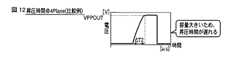
より具体的に、図11乃至図13を用い、シングルプレーン動作時と同様の時間で、所定の電圧まで昇圧することができる点について説明する。
図11は、第1の実施形態での、1プレーン選択(@1Plane)での昇圧時間と昇圧電圧との関係を示している。図示するように、所定の出力電圧VPPOUTとなるまで、時間ΔT1程度[μs]必要である。
図12は、後述する比較例での、4プレーン選択(@4Plane)での昇圧時間と昇圧電圧との関係を示している。図示するように、所定の出力電圧VPPOUTとなるまで、上記時間ΔT1よりも大きい時間ΔT2程度[μs]必要である(ΔT1<ΔT2)。
図13は、第1の実施形態での、4プレーン選択(@4Plane)での昇圧時間と昇圧電圧との関係を示している。図示するように、4プレーン選択であっても、所定の出力電圧VPPOUTとなるまで、時間ΔT1と同様の時間ΔT3程度[μs]で昇圧することができ、昇圧時間が低減されていることが分かる(ΔT3(=ΔT1)<ΔT2)。
このように、本例に係る構成および動作によれば、シングルプレーン動作時と同様の時間で所定の電圧まで昇圧することができ、昇圧時間を低減できる点で有利である。そのため、例えば、テスト時間を短縮できる点で有効である。More specifically, the point that the voltage can be boosted to a predetermined voltage in the same time as in the single plane operation will be described with reference to FIGS.
FIG. 11 shows the relationship between the boost time and the boost voltage in one plane selection (@ 1 Plane) in the first embodiment. As shown in the figure, it takes about [Delta] T1 [[mu] s] until a predetermined output voltage VPPOUT is reached.
FIG. 12 shows the relationship between the boosting time and the boosted voltage when selecting 4 planes (@ 4 Plane) in a comparative example described later. As shown in the figure, it takes about [Delta] T2 [.DELTA.T1 <.DELTA.T2] that is larger than the above time .DELTA.T1 until the predetermined output voltage VPPOUT is reached.
FIG. 13 shows the relationship between the boosting time and the boosted voltage in the 4-plane selection (@ 4 Plane) in the first embodiment. As shown in the figure, even when four planes are selected, the voltage can be boosted in about [Delta] T3 [[mu] s] similar to the time [Delta] T1 until the predetermined output voltage VPPOUT is reached, and the boosting time is reduced. (ΔT3 (= ΔT1) <ΔT2).
As described above, according to the configuration and operation according to this example, it is possible to boost the voltage to a predetermined voltage in the same time as in the single plane operation, and it is advantageous in that the boost time can be reduced. Therefore, for example, it is effective in that the test time can be shortened.
加えて、本例に係る構成およびその昇圧動作によれば、昇圧回路32の昇圧能力を向上できるため、ポンプ回路の数を低減することができる。換言すると、昇圧回路32は、上記のように、N個(Nは2以上の整数)のプレーンを備えるメモリセルアレイの場合、プレーン数(N個)より少ない、少なくとも(N−1)個のプレーンの電圧を昇圧させるように構成できる。より具体的には、図7に示す昇圧回路32のVPPポンプ,VREADポンプ,VRDポンプの数をそれぞれ低減することができる。例えば、本例の場合、後述する比較例と比べ、VPPポンプ,VREADポンプ,VRDポンプの数を、半分程度(VPPポンプ:4個→2個,VREADポンプ:2個→1個,VRDポンプ:2個→1個)とすることができる。この結果、チップサイズを低減でき、微細化に対して有利である。 In addition, according to the configuration according to this example and the boosting operation thereof, the boosting capability of the
以上のように、本第1の実施形態に係る半導体記憶装置の構成およびその昇圧動作によれば、メモリセルアレイ11が複数プレーン構成であっても、電源電圧発生回路19の昇圧時間の低減化および微細化に対して有利である。 As described above, according to the configuration of the semiconductor memory device and the boosting operation thereof according to the first embodiment, the boosting time of the power supply
(2)必要に応じて、昇圧条件を設定することができる。
上記のように、昇圧能力制御回路33に入力される信号A,信号Bは、例えば、テストモード時に限らず、マルチページプログラム等の複数プレーンを選択して駆動する通常動作時等においても、信号A,信号Bを変更することにより、昇圧回路32の周期および電源を変更できる。そのため、使用プレーンの状態の必要に応じて、昇圧条件を設定できる点で有利である。(2) Boosting conditions can be set as necessary.
As described above, the signals A and B input to the boosting capability control circuit 33 are not limited to, for example, in the test mode, but also in the normal operation of selecting and driving a plurality of planes such as a multi-page program. By changing A and signal B, the period and power supply of the
例えば、昇圧条件の設定は、通常のコマンドシーケンス後に、昇圧コマンド(信号A)を入力するか否かにより、自由に行うことができる。また、例えば、昇圧条件の設定は、メモリセルアレイ11中のROMセル(MT)が記憶するデータを書き換えて信号Bを変更することにより、自由に行うことができる。 For example, the boost condition can be set freely depending on whether or not a boost command (signal A) is input after a normal command sequence. Further, for example, the boost condition can be set freely by rewriting data stored in the ROM cell (MT) in the
また、本例に係る構成を適用することで、シングルプレーン動作時においてはマルチプレーン動作時の負荷容量に対応した過剰な昇圧能力は不要となるため、昇圧回路32のピーク電流の削減効果も期待でき、消費電力の低減に対して有利である。さらに、上記(1)に説明したように、VPPポンプ,VREADポンプ,VRDポンプの数を低減できるため、製造コストの低減に対してもメリットがあると言える。 In addition, by applying the configuration according to this example, an excessive boosting capability corresponding to the load capacity at the time of multiplane operation becomes unnecessary during single plane operation, so that the peak current reduction effect of the
[第2の実施形態(更に複数のクロック発生回路を備える一例)]
次に、図14を用いて、第2の実施形態に係る半導体記憶装置について説明する。この実施形態は、更に複数のクロック発生回路を備える一例に関するものである。この説明において、上記第1の実施形態と重複する部分の詳細な説明を省略する。[Second Embodiment (an example further including a plurality of clock generation circuits)]
Next, a semiconductor memory device according to the second embodiment will be described with reference to FIG. This embodiment relates to an example further including a plurality of clock generation circuits. In this description, detailed description of the same parts as those in the first embodiment is omitted.
<構成例>
図示するように、第2の実施形態では、クロック生成回路20が更に複数の短周期の第3クロック生成回路20−3及び第4クロック生成回路20−4を備え、昇圧能力制御回路33においてクロック選択信号生成回路33−3を更に備え、周期制御回路部33−2が更に第3選択回路SC及び第4選択回路SDを備える点で、上記第1の実施形態と相違する。<Configuration example>
As illustrated, in the second embodiment, the
第3選択回路SC及び第4選択回路SDには、第1クロックCLKAよりも順次短く第2クロックCLKBよりも長い周期の複数のクロック(第3クロックCLKC及び第4クロックCLKD)がそれぞれ入力される。本例では、4個のプレーンが備えられているため、第1及び第2の選択回路SA,SBに加えて、2個の選択回路が追加されている。N個のプレーンが備えられている場合は、(N−2)個の選択回路が追加される。すなわち、第1選択回路SA、第2選択回路SB、及び(N−2)個の追加選択回路からなる合計N個の選択回路がN個のプレーンに対応して設けられる。
クロック生成回路20は、更に複数の短周期の第3クロック生成回路20−3、第4クロック生成回路20−4を備える。第3クロック生成回路20−3は第3クロックCLKCを発生させる。第4クロック生成回路20−4は第4クロックCLKDを発生させる。発生する周期の関係は、基準周期A(第1クロックCLKA)>短周期D(第4クロックCLKD)>短周期C(第3クロックCLKC)>短周期B(第2クロックCLKB)、である。A plurality of clocks (third clock CLKC and fourth clock CLKD) having a period shorter than the first clock CLKA and longer than the second clock CLKB are input to the third selection circuit SC and the fourth selection circuit SD, respectively. . In this example, since four planes are provided, two selection circuits are added in addition to the first and second selection circuits SA and SB. When N planes are provided, (N−2) selection circuits are added. That is, a total of N selection circuits including the first selection circuit SA, the second selection circuit SB, and (N−2) additional selection circuits are provided corresponding to the N planes.
The
クロック選択信号生成回路33−3には、信号Cおよびプレーン選択信号PB<3:0>が入力され、選択プレーン数に応じた信号CB,CC,CDを、周期制御部33−2に出力する。例えば、クロック選択信号生成回路33−3は、2プレーン選択時に信号CDによって第4選択回路SDが活性化され、3プレーン選択時に信号CCによって第3選択回路SCが活性化され、4プレーン選択時に信号CBによって第2選択回路SBが活性化されるように制御する。すなわち、選択プレーン数に応じていずれか1つの選択回路が活性化され、それ以外の選択回路が非活性化される。 The clock selection signal generation circuit 33-3 receives the signal C and the plane selection signal PB <3: 0>, and outputs signals CB, CC, and CD corresponding to the number of selected planes to the cycle control unit 33-2. . For example, in the clock selection signal generation circuit 33-3, the fourth selection circuit SD is activated by the signal CD when the two planes are selected, the third selection circuit SC is activated by the signal CC when the three planes are selected, and the four selection planes are selected. Control is performed so that the second selection circuit SB is activated by the signal CB. That is, any one selection circuit is activated according to the number of selection planes, and the other selection circuits are deactivated.
周期制御回路部33−2は、入力される信号C,CB,CC,CDに応じて、昇圧回路32に与える周期PMPCLKを切り替えて出力する。例えば、2プレーン選択の場合、昇圧回路32に与える周期を、基準周期Aから短周期Dに切り替えて出力する。同様に、3プレーン選択の場合、昇圧回路32に与える周期を、基準周期Aから短周期Cに切り替えて出力する。同様に、4プレーン選択の場合、昇圧回路32に与える周期を、基準周期Aから短周期Bに切り替えて出力する。 The cycle control circuit unit 33-2 switches and outputs a cycle PMPCLK to be given to the
その他の構成および昇圧動作については、上記第1の実施形態と実質的に同様であるため、その詳細な説明を省略する。 Other configurations and boosting operations are substantially the same as those in the first embodiment, and a detailed description thereof will be omitted.
<作用効果>
上記のように、第2の実施形態に係る半導体記憶装置およびその昇圧動作によれば、少なくとも上記(1)乃至(2)と同様の効果が得られる。さらに、本例によれば、下記(3)の効果を得ることができる。
(3)昇圧回路32の周期をより細かく制御でき、選択プレーン数に合わせたより細かい制御を行うことができる。
上記のように、第2の実施形態に係る周期制御回路部33−2は、入力される信号C,CB,CC,CDに応じて、昇圧回路32に与える周期PMPCLKを切り替えて出力する。例えば、2プレーン選択の場合、昇圧回路32に与える周期を、基準周期Aから短周期Dに切り替えて出力する。同様に、3プレーン選択の場合、昇圧回路32に与える周期を、基準周期Aから短周期Cに切り替えて出力する。同様に、4プレーン選択の場合、昇圧回路32に与える周期を、基準周期Aから短周期Bに切り替えて出力する。<Effect>
As described above, according to the semiconductor memory device and the boosting operation thereof according to the second embodiment, at least the same effects as the above (1) to (2) can be obtained. Furthermore, according to this example, the following effect (3) can be obtained.
(3) The period of the
As described above, the cycle control circuit unit 33-2 according to the second embodiment switches and outputs the cycle PMPCLK supplied to the
そのため、プレーン選択信号PB<3:0>の信号を受けて、クロックの周期を変更することにより、昇圧回路32の周期をより細かく制御でき、選択プレーン数に合わせたより細かい制御を行うことができる点で有利である。 Therefore, by receiving the plane selection signals PB <3: 0> and changing the clock cycle, the cycle of the
[第3の実施形態(外部パッドからクロックを選択する一例)]
次に、図15を用いて、第3の実施形態に係る半導体記憶装置について説明する。この実施形態は、例えばテストモード時において外部パッドから与えられるクロックを選択する一例に関するものである。この説明において、上記第1の実施形態と重複する部分の詳細な説明を省略する。[Third embodiment (an example of selecting a clock from an external pad)]
Next, a semiconductor memory device according to the third embodiment will be described with reference to FIG. This embodiment relates to an example of selecting a clock provided from an external pad in the test mode, for example. In this description, detailed description of the same parts as those in the first embodiment is omitted.
<構成例>
図示するように、第3の実施形態に係る半導体記憶装置では、周期制御部33−2がトランジスタN41、N42を備える点で、上記第1の実施形態と相違する。トランジスタN41、N42は、選択回路SBの入力を、クロック発生回路20−2から入力される第2クロックCLKBかまたは外部PADから入力される外部クロックかのいずれか一方に切り替えるスイッチング素子として働く。
トランジスタN41の電流経路の一端は選択回路SBの入力に接続され、電流経路の他端には第2クロックCLKBが入力され、制御端子には、制御信号Dの反転信号〜Dが入力される。<Configuration example>
As illustrated, the semiconductor memory device according to the third embodiment is different from the first embodiment in that the cycle control unit 33-2 includes transistors N41 and N42. The transistors N41 and N42 function as switching elements that switch the input of the selection circuit SB to either the second clock CLKB input from the clock generation circuit 20-2 or the external clock input from the external PAD.
One end of the current path of the transistor N41 is connected to the input of the selection circuit SB, the second clock CLKB is input to the other end of the current path, and inverted signals to D of the control signal D are input to the control terminal.
トランジスタN42の電流経路の一端は選択回路SBの入力に接続され、電流経路の他端には外部PADが電気的に接続され、制御端子には、制御信号Dが入力される。尚、上記制御信号D、〜Dは、例えば、図示しない制御回路17等から生成され、与えられる。 One end of the current path of the transistor N42 is connected to the input of the selection circuit SB, the external PAD is electrically connected to the other end of the current path, and the control signal D is input to the control terminal. The control signals D,..., D are generated and given from, for example, a control circuit 17 (not shown).
制御回路17から入力される信号Dのレベルが切り替わると、トランジスタN41がオフとされ、トランジスタN42がオンとされる。制御信号Cが“H”である場合に、選択回路SBは、昇圧回路32に与える周期PMPCLKを、第2クロックCLKBから、外部PADから与えられ上記第1クロックCLKA及び第2クロックCLKBとは周期の異なる外部クロック(クロックCLKP1及びクロックCLKP2)に切り替えて選択的に出力する。 When the level of the signal D input from the
外部PADは、例えばテストモード用に設けられた専用PADであって、外部テスタ機器等と電気的に接続される。外部PADから与えるクロックは1種類であっても良いし、2種類以上であっても良い。本例では、2種類の外部クロック(クロックCLKP1及びクロックCLKP2)が外部PADに入力される場合を示している。 The external PAD is a dedicated PAD provided for test mode, for example, and is electrically connected to an external tester device or the like. There may be one type of clock provided from the external PAD, or two or more types. In this example, two types of external clocks (clock CLKP1 and clock CLKP2) are input to the external PAD.
このように本例では、外部から所定周期のクロックを昇圧回路32に与えることができる。例えば、外部PADから昇圧回路32にクロックCLKP1(周期C)、またはCLKP2(周期D)を与えることができる。発生する周期の関係は、本例では、基準周期A>短周期B>短周期C>短周期D、であるとする。尚、外部PADから入力する周期の関係はこれに限定されず、例えばテストモード時の評価において必要とされる様々な周期のクロックを入力することが可能である。 As described above, in this example, a clock having a predetermined cycle can be supplied to the
上記構成によれば、周期制御部33−2は、入力される信号Dのレベルが切り替わると、トランジスタN41をオフ、トランジスタN41をオンとし、昇圧回路32に与える周期PMPCLKを、第2クロックCLKBから、外部PADから与えられる外部クロック(CLKP1,CLKP2)に切り替えて出力する。 According to the above configuration, when the level of the input signal D is switched, the cycle control unit 33-2 turns off the transistor N41, turns on the transistor N41, and sets the cycle PMPCLK to be given to the
そのため、信号Dを受けて、クロックの周期を、外部PADから与えられる任意の周期の外部クロックに変更することにより、昇圧回路32の周期をより細かく制御でき、選択プレーン数に合わせたより細かい制御を行うことができる点で有利である。これにより、例えばテストモード時において複数プレーンを同時に選択することが可能となり、テスト時間の短縮を図ることができる。 Therefore, by receiving the signal D and changing the clock cycle to an external clock having an arbitrary cycle given from the external PAD, the cycle of the
<作用効果>
上記のように、第3の実施形態に係る半導体記憶装置およびその昇圧動作によれば、少なくとも上記(1)乃至(3)と同様の効果が得られる。
さらに、本例によれば、必要に応じて、クロック生成回路20−2のクロックの使用を停止し、外部PADから任意の周期の外部クロックを印加できる点で有利である。<Effect>
As described above, according to the semiconductor memory device and its boosting operation according to the third embodiment, at least the same effects as the above (1) to (3) can be obtained.
Furthermore, this example is advantageous in that the use of the clock of the clock generation circuit 20-2 can be stopped and an external clock having an arbitrary period can be applied from the external PAD as necessary.
[比較例]
次に、図16および図17を用い、上記第1乃至第3の実施形態に係る半導体記憶装置と比較するために、比較例に係る半導体記憶装置について説明する。この説明において、上記第1の実施形態と重複する部分の詳細な説明を省略する。[Comparative example]
Next, in order to compare with the semiconductor memory device according to the first to third embodiments, a semiconductor memory device according to a comparative example will be described with reference to FIGS. In this description, detailed description of the same parts as those in the first embodiment is omitted.
<構成例>
図16に示すように、比較例に係る電源電圧発生回路119では、上記第1乃至第3の実施形態に係る昇圧能力制御回路33を具備していない点で、上記実施形態と相違する。そのため、昇圧回路に入力される周期PMPCLKおよび基準電圧PMPDRREFを、選択プレーン数に応じて切り替えて制御することができない構成である。<Configuration example>
As shown in FIG. 16, the power supply
そのため、比較例に係る昇圧回路は、図17のように示される。
図示するように、VPP昇圧回路132−1は、4つのVPPポンプPP1,PP2,PP3,PP4、検知回路を備える。VREAD昇圧回路132−2は、2つのVREADポンプRP1、RP2、検知回路を備える。VRD昇圧回路132−3は、2つのVRDポンプDP1、DP2、検知回路を備える。
図中の破線で囲って示すように、比較例に係る昇圧回路132におけるVPPポンプ,VREADポンプ,VRDポンプの数がそれぞれ増大していることが分かる。例えば、比較例の場合、上記実施形態と比べ、VPPポンプ,VREADポンプ,VRDポンプの数が倍程度(VPPポンプ:2個→4個,VREADポンプ:1個→2個,VRDポンプ:1個→2個)に増大していることが明らかである。このように、比較例では、チップサイズが増大し、微細化に対して不利である。Therefore, the booster circuit according to the comparative example is shown as in FIG.
As illustrated, the VPP booster circuit 132-1 includes four VPP pumps PP1, PP2, PP3, PP4, and a detection circuit. The VREAD booster circuit 132-2 includes two VREAD pumps RP1 and RP2 and a detection circuit. The VRD booster circuit 132-3 includes two VRD pumps DP1 and DP2 and a detection circuit.
As indicated by the broken lines in the figure, it can be seen that the numbers of VPP pumps, VREAD pumps, and VRD pumps in the
以上、第1乃至第3の実施形態および比較例を用いて本発明の説明を行ったが、この発明は上記各実施形態に限定されるものではなく、実施段階ではその要旨を逸脱しない範囲で種々に変形することが可能である。また、上記各実施形態には種々の段階の発明が含まれており、開示される複数の構成要件の適宜な組み合わせにより種々の発明が抽出され得る。例えば各実施形態に示される全構成要件からいくつかの構成要件が削除されても、発明が解決しようとする課題の欄で述べた課題の少なくとも1つが解決でき、発明の効果の欄で述べられている効果の少なくとも1つが得られる場合には、この構成要件が削除された構成が発明として抽出され得る。 The present invention has been described above using the first to third embodiments and the comparative example. However, the present invention is not limited to the above-described embodiments, and the scope of the invention is not deviated from the scope of the invention. Various modifications are possible. Each of the above embodiments includes inventions at various stages, and various inventions can be extracted by appropriately combining a plurality of disclosed constituent elements. For example, even if some constituent elements are deleted from all the constituent elements shown in each embodiment, at least one of the problems described in the column of the problem to be solved by the invention can be solved, and is described in the column of the effect of the invention. When at least one of the effects is obtained, a configuration in which this configuration requirement is deleted can be extracted as an invention.
11…メモリセルアレイ、19…電源電圧発生回路、20…クロック発生回路、31…基準電圧生成回路、32…昇圧回路、33…昇圧能力制御回路、33−1…基準電圧制御部、33−2…周期制御部。DESCRIPTION OF
Claims (10)
Translated fromJapanese第1基準電圧および前記第1基準電圧よりも高い第2基準電圧を発生させる基準電圧生成回路と、
前記基準電圧生成回路から与えられる前記第1または第2基準電圧を昇圧した昇圧電圧を前記プレーンに供給する昇圧回路と、
(N−1)個以下の前記プレーンを選択する場合は前記第1基準電圧を前記昇圧回路に与え、N個の前記プレーンを選択する場合は前記第2基準電圧を前記昇圧回路に与える昇圧能力制御回路と、を具備すること
を特徴とする半導体記憶装置。A memory cell array comprising N (N is an integer of 2 or more) planes each having a plurality of memory cells;
A reference voltage generation circuit for generating a first reference voltage and a second reference voltage higher than the first reference voltage;
A booster circuit that supplies a boosted voltage obtained by boosting the first or second reference voltage supplied from the reference voltage generation circuit to the plane;
When selecting (N−1) or less planes, the first reference voltage is supplied to the booster circuit, and when selecting N planes, the booster capability is to apply the second reference voltage to the booster circuit. A semiconductor memory device, comprising: a control circuit;
前記昇圧能力制御回路は、(N−1)個以下の前記プレーンを選択する場合は前記第1クロックを前記昇圧回路に入力し、N個の前記プレーンを選択する場合は前記第2クロックを前記昇圧回路に入力すること
を特徴とする請求項1に記載の半導体記憶装置。A clock generation circuit for generating a first clock and a second clock having a shorter cycle than the first clock;
The boosting capacity control circuit inputs the first clock to the booster circuit when selecting the (N−1) or less planes, and the second clock when selecting the N planes. The semiconductor memory device according to claim 1, wherein the semiconductor memory device is input to a booster circuit.
前記昇圧能力制御回路は、
前記シングルプレーン動作を実行する場合に前記基準電圧生成回路が前記第1基準電圧を発生させ、前記マルチプレーン動作を実行する場合に前記基準電圧生成回路が前記第2基準電圧を発生させるように制御する基準電圧制御部と、
前記シングルプレーン動作を実行する場合に前記第1クロックを前記昇圧回路に入力させ、前記マルチプレーン動作を実行する場合に前記第2クロックを前記昇圧回路に入力させるように制御する周期制御部と、を備えること
を特徴とする請求項1または2に記載の半導体記憶装置。The semiconductor memory device can perform a single plane operation for selecting and driving one plane and a multi-plane operation for selecting and driving N planes.
The boosting capacity control circuit includes:
Control is performed such that the reference voltage generation circuit generates the first reference voltage when the single plane operation is performed, and the reference voltage generation circuit generates the second reference voltage when the multiplane operation is performed. A reference voltage control unit,
A period controller for controlling the first clock to be input to the booster circuit when the single plane operation is performed, and the second clock to be input to the booster circuit when the multiplane operation is performed; The semiconductor memory device according to claim 1, further comprising:
前記周期制御部は、前記第1クロックが入力される第1選択回路と、前記第2クロックが入力される第2選択回路とを有し、
前記第1及び第2選択回路は、前記制御信号に応じて、前記第1及び第2クロックのいずれか一方を選択的に出力すること
を特徴とする請求項3に記載の半導体記憶装置。The reference voltage control unit has an OR circuit that receives ROM cell data and command data given from a ROM cell in the memory cell array and outputs a control signal.
The cycle control unit includes a first selection circuit to which the first clock is input, and a second selection circuit to which the second clock is input.
4. The semiconductor memory device according to claim 3, wherein the first and second selection circuits selectively output one of the first and second clocks according to the control signal. 5.
前記クロック生成回路は、前記第1クロックよりも順次短く前記第2クロックよりも長い周期の(N−2)個のクロックを更に発生させ、
前記周期制御部は、前記(N−2)個のクロックがそれぞれ入力される(N−2)個の選択回路を更に有し、
前記第1、第2選択回路、及び前記(N−2)個の選択回路は、前記制御信号及び前記クロック選択信号に応じて、前記第1、第2、及び前記(N−2)個のクロックのいずれか1つを選択的に出力すること
を特徴とする請求項4に記載の半導体記憶装置。The boost capability control circuit further includes a clock selection signal generation circuit that receives the control signal and generates a plurality of clock selection signals,
The clock generation circuit further generates (N−2) clocks that are sequentially shorter than the first clock and longer than the second clock,
The cycle control unit further includes (N-2) selection circuits to which the (N-2) clocks are input,
The first, second selection circuit, and the (N−2) selection circuits are configured to correspond to the first, second, and (N−2) selection circuits according to the control signal and the clock selection signal. The semiconductor memory device according to claim 4, wherein any one of the clocks is selectively output.
前記周期制御部は、前記第1クロックが入力される第1選択回路と、前記第2クロックまたは外部から与えられ、前記第1及び第2クロックとは周期の異なる第3クロックが入力される第2選択回路とを有し、
前記第2選択回路は、前記制御信号に応じて、前記第2及び第3クロックのいずれか一方を選択的に出力すること
を特徴とする請求項3に記載の半導体記憶装置。The reference voltage control unit has an OR circuit that receives ROM cell data and command data given from a ROM cell in the memory cell array and outputs a control signal.
The cycle control unit receives a first selection circuit to which the first clock is input and a second clock which is supplied from the second clock or externally and has a cycle different from that of the first and second clocks. 2 selection circuit,
The semiconductor memory device according to claim 3, wherein the second selection circuit selectively outputs one of the second and third clocks according to the control signal.
前記メモリセルアレイのデータ書込みのための電圧を発生させる少なくとも1つのVPPポンプ回路と、
前記メモリセルアレイのデータ読出しのための電圧を発生させる少なくとも1つのVREADポンプ回路と、
前記メモリセルアレイのデコーダを駆動させるための電源電圧を発生させる少なくとも1つのVRDポンプ回路と、を有すること
を特徴とする請求項1乃至6のいずれか1項に記載の半導体記憶装置。The booster circuit includes:
At least one VPP pump circuit for generating a voltage for writing data in the memory cell array;
At least one VREAD pump circuit for generating a voltage for reading data from the memory cell array;
The semiconductor memory device according to claim 1, further comprising: at least one VRD pump circuit that generates a power supply voltage for driving a decoder of the memory cell array.
を特徴とする請求項7に記載の半導体記憶装置。The boosting capacity control circuit generates a voltage for data writing in a common boosting time even when the number of selected planes is different when writing data in the memory cell array. The semiconductor memory device according to claim 7, wherein the VPP pump circuit is controlled.
を特徴とする請求項7に記載の半導体記憶装置。The boosting capacity control circuit generates a voltage for reading the data in a common boosting time even when the number of selected planes is different when reading data from the memory cell array. The semiconductor memory device according to claim 7, wherein the VREAD pump circuit is controlled.
を特徴とする請求項7に記載の半導体記憶装置。The boosting capability control circuit generates a power supply voltage for driving the decoder in a common boosting time even when the number of selected planes is different when driving the decoder of the memory cell array. The semiconductor memory device according to claim 7, further comprising: controlling the VRD pump circuit.
Priority Applications (1)
| Application Number | Priority Date | Filing Date | Title |
|---|---|---|---|
| JP2009265450AJP2011108349A (en) | 2009-11-20 | 2009-11-20 | Semiconductor memory device |
Applications Claiming Priority (1)
| Application Number | Priority Date | Filing Date | Title |
|---|---|---|---|
| JP2009265450AJP2011108349A (en) | 2009-11-20 | 2009-11-20 | Semiconductor memory device |
Publications (1)
| Publication Number | Publication Date |
|---|---|
| JP2011108349Atrue JP2011108349A (en) | 2011-06-02 |
Family
ID=44231637
Family Applications (1)
| Application Number | Title | Priority Date | Filing Date |
|---|---|---|---|
| JP2009265450AWithdrawnJP2011108349A (en) | 2009-11-20 | 2009-11-20 | Semiconductor memory device |
Country Status (1)
| Country | Link |
|---|---|
| JP (1) | JP2011108349A (en) |
Cited By (5)
| Publication number | Priority date | Publication date | Assignee | Title |
|---|---|---|---|---|
| JP2017054574A (en)* | 2015-09-11 | 2017-03-16 | 株式会社東芝 | Voltage generation circuit and semiconductor memory device |
| US10811107B2 (en) | 2019-02-22 | 2020-10-20 | Samsung Electronics Co., Ltd. | Semiconductor memory device and memory system having the same |
| CN113689895A (en)* | 2020-05-19 | 2021-11-23 | 爱思开海力士有限公司 | Voltage generator and memory device having the same |
| US11551767B2 (en) | 2020-09-09 | 2023-01-10 | Kioxia Corporation | Semiconductor storage device having boosting circuits with different boosting capacities |
| US11815925B2 (en) | 2021-02-25 | 2023-11-14 | Kioxia Corporation | Power source circuit, input and output circuit, semiconductor storage device, and power supply control method |
- 2009
- 2009-11-20JPJP2009265450Apatent/JP2011108349A/ennot_activeWithdrawn
Cited By (5)
| Publication number | Priority date | Publication date | Assignee | Title |
|---|---|---|---|---|
| JP2017054574A (en)* | 2015-09-11 | 2017-03-16 | 株式会社東芝 | Voltage generation circuit and semiconductor memory device |
| US10811107B2 (en) | 2019-02-22 | 2020-10-20 | Samsung Electronics Co., Ltd. | Semiconductor memory device and memory system having the same |
| CN113689895A (en)* | 2020-05-19 | 2021-11-23 | 爱思开海力士有限公司 | Voltage generator and memory device having the same |
| US11551767B2 (en) | 2020-09-09 | 2023-01-10 | Kioxia Corporation | Semiconductor storage device having boosting circuits with different boosting capacities |
| US11815925B2 (en) | 2021-02-25 | 2023-11-14 | Kioxia Corporation | Power source circuit, input and output circuit, semiconductor storage device, and power supply control method |
Similar Documents
| Publication | Publication Date | Title |
|---|---|---|
| US8867278B2 (en) | Nonvolatile memory device, memory system including the same, and method of operating nonvolatile memory device | |
| US8144525B2 (en) | Memory cell sensing using negative voltage | |
| JP3913952B2 (en) | Semiconductor memory device | |
| JP6482690B1 (en) | Semiconductor memory device | |
| CN112447206B (en) | Method and apparatus for driving an access line to a target voltage level | |
| US11705163B1 (en) | Nonvolatile memory devices, systems and methods with switching charge pump architectures | |
| CN113924624B (en) | Memory device including voltage generating system | |
| CN112447246B (en) | Apparatus and method for mitigating program disturb | |
| JP2012027988A (en) | Semiconductor storage device and control method for the same | |
| CN101295543A (en) | Method of reducing write time in non-volatile memory devices and related devices | |
| TWI375954B (en) | Expanded programming window for non-volatile multilevel memory cells | |
| US20120106251A1 (en) | Flash memory device configured to switch wordline and initialization voltages | |
| KR20150134438A (en) | Sharing support circuitry in a memory | |
| JP2021121982A (en) | Method of program prohibition in memory device | |
| JP2011108349A (en) | Semiconductor memory device | |
| US11127474B2 (en) | Memory device | |
| US10971202B1 (en) | Low latency data transfer | |
| JP4790335B2 (en) | Nonvolatile semiconductor memory device | |
| US9019765B2 (en) | Semiconductor device, data programming device, and method for improving the recovery of bit lines of unselected memory cells for programming operation | |
| JP2008004196A (en) | Semiconductor memory device | |
| JP2001085633A (en) | Semiconductor device having capacitance structure, charge pump circuit using the capacitance structure, and semiconductor device using charge pump circuit | |
| JP2008181661A (en) | Nonvolatile semiconductor memory device | |
| WO2006090442A1 (en) | Semiconductor device and method for controlling the same | |
| US20240233835A1 (en) | Semiconductor device | |
| KR101081874B1 (en) | Method of volgate offering a non volatile memory device |
Legal Events
| Date | Code | Title | Description |
|---|---|---|---|
| A300 | Withdrawal of application because of no request for examination | Free format text:JAPANESE INTERMEDIATE CODE: A300 Effective date:20130205 |