JP2011082526A - Method of growing group iii-v layer on silicon using nano-scale orientation pattern - Google Patents
Method of growing group iii-v layer on silicon using nano-scale orientation patternDownload PDFInfo
- Publication number
- JP2011082526A JP2011082526AJP2010228979AJP2010228979AJP2011082526AJP 2011082526 AJP2011082526 AJP 2011082526AJP 2010228979 AJP2010228979 AJP 2010228979AJP 2010228979 AJP2010228979 AJP 2010228979AJP 2011082526 AJP2011082526 AJP 2011082526A
- Authority
- JP
- Japan
- Prior art keywords
- silicon substrate
- recess
- iii
- forming
- compound semiconductor
- Prior art date
- Legal status (The legal status is an assumption and is not a legal conclusion. Google has not performed a legal analysis and makes no representation as to the accuracy of the status listed.)
- Granted
Links
Images


Classifications
- H—ELECTRICITY
- H01—ELECTRIC ELEMENTS
- H01L—SEMICONDUCTOR DEVICES NOT COVERED BY CLASS H10
- H01L21/00—Processes or apparatus adapted for the manufacture or treatment of semiconductor or solid state devices or of parts thereof
- H01L21/02—Manufacture or treatment of semiconductor devices or of parts thereof
- H01L21/02104—Forming layers
- H01L21/02365—Forming inorganic semiconducting materials on a substrate
- H01L21/02518—Deposited layers
- H01L21/02521—Materials
- H01L21/02538—Group 13/15 materials
- H01L21/02546—Arsenides
- H—ELECTRICITY
- H01—ELECTRIC ELEMENTS
- H01L—SEMICONDUCTOR DEVICES NOT COVERED BY CLASS H10
- H01L21/00—Processes or apparatus adapted for the manufacture or treatment of semiconductor or solid state devices or of parts thereof
- H01L21/02—Manufacture or treatment of semiconductor devices or of parts thereof
- H01L21/02104—Forming layers
- H01L21/02365—Forming inorganic semiconducting materials on a substrate
- H01L21/02367—Substrates
- H01L21/0237—Materials
- H01L21/02373—Group 14 semiconducting materials
- H01L21/02381—Silicon, silicon germanium, germanium
- H—ELECTRICITY
- H01—ELECTRIC ELEMENTS
- H01L—SEMICONDUCTOR DEVICES NOT COVERED BY CLASS H10
- H01L21/00—Processes or apparatus adapted for the manufacture or treatment of semiconductor or solid state devices or of parts thereof
- H01L21/02—Manufacture or treatment of semiconductor devices or of parts thereof
- H01L21/02104—Forming layers
- H01L21/02365—Forming inorganic semiconducting materials on a substrate
- H01L21/02367—Substrates
- H01L21/02433—Crystal orientation
- H—ELECTRICITY
- H01—ELECTRIC ELEMENTS
- H01L—SEMICONDUCTOR DEVICES NOT COVERED BY CLASS H10
- H01L21/00—Processes or apparatus adapted for the manufacture or treatment of semiconductor or solid state devices or of parts thereof
- H01L21/02—Manufacture or treatment of semiconductor devices or of parts thereof
- H01L21/02104—Forming layers
- H01L21/02365—Forming inorganic semiconducting materials on a substrate
- H01L21/02518—Deposited layers
- H01L21/02609—Crystal orientation
- H—ELECTRICITY
- H01—ELECTRIC ELEMENTS
- H01L—SEMICONDUCTOR DEVICES NOT COVERED BY CLASS H10
- H01L21/00—Processes or apparatus adapted for the manufacture or treatment of semiconductor or solid state devices or of parts thereof
- H01L21/02—Manufacture or treatment of semiconductor devices or of parts thereof
- H01L21/02104—Forming layers
- H01L21/02365—Forming inorganic semiconducting materials on a substrate
- H01L21/02612—Formation types
- H01L21/02617—Deposition types
- H01L21/02636—Selective deposition, e.g. simultaneous growth of mono- and non-monocrystalline semiconductor materials
- H01L21/02639—Preparation of substrate for selective deposition
- H—ELECTRICITY
- H01—ELECTRIC ELEMENTS
- H01L—SEMICONDUCTOR DEVICES NOT COVERED BY CLASS H10
- H01L21/00—Processes or apparatus adapted for the manufacture or treatment of semiconductor or solid state devices or of parts thereof
- H01L21/70—Manufacture or treatment of devices consisting of a plurality of solid state components formed in or on a common substrate or of parts thereof; Manufacture of integrated circuit devices or of parts thereof
- H01L21/71—Manufacture of specific parts of devices defined in group H01L21/70
- H01L21/76—Making of isolation regions between components
- H01L21/762—Dielectric regions, e.g. EPIC dielectric isolation, LOCOS; Trench refilling techniques, SOI technology, use of channel stoppers
- H01L21/76224—Dielectric regions, e.g. EPIC dielectric isolation, LOCOS; Trench refilling techniques, SOI technology, use of channel stoppers using trench refilling with dielectric materials
- H—ELECTRICITY
- H10—SEMICONDUCTOR DEVICES; ELECTRIC SOLID-STATE DEVICES NOT OTHERWISE PROVIDED FOR
- H10D—INORGANIC ELECTRIC SEMICONDUCTOR DEVICES
- H10D30/00—Field-effect transistors [FET]
- H10D30/01—Manufacture or treatment
- H10D30/021—Manufacture or treatment of FETs having insulated gates [IGFET]
- H—ELECTRICITY
- H10—SEMICONDUCTOR DEVICES; ELECTRIC SOLID-STATE DEVICES NOT OTHERWISE PROVIDED FOR
- H10D—INORGANIC ELECTRIC SEMICONDUCTOR DEVICES
- H10D62/00—Semiconductor bodies, or regions thereof, of devices having potential barriers
- H10D62/10—Shapes, relative sizes or dispositions of the regions of the semiconductor bodies; Shapes of the semiconductor bodies
- H10D62/117—Shapes of semiconductor bodies
- H10D62/118—Nanostructure semiconductor bodies
- H—ELECTRICITY
- H10—SEMICONDUCTOR DEVICES; ELECTRIC SOLID-STATE DEVICES NOT OTHERWISE PROVIDED FOR
- H10D—INORGANIC ELECTRIC SEMICONDUCTOR DEVICES
- H10D62/00—Semiconductor bodies, or regions thereof, of devices having potential barriers
- H10D62/40—Crystalline structures
- H10D62/405—Orientations of crystalline planes
- H—ELECTRICITY
- H10—SEMICONDUCTOR DEVICES; ELECTRIC SOLID-STATE DEVICES NOT OTHERWISE PROVIDED FOR
- H10D—INORGANIC ELECTRIC SEMICONDUCTOR DEVICES
- H10D62/00—Semiconductor bodies, or regions thereof, of devices having potential barriers
- H10D62/80—Semiconductor bodies, or regions thereof, of devices having potential barriers characterised by the materials
- H10D62/85—Semiconductor bodies, or regions thereof, of devices having potential barriers characterised by the materials being Group III-V materials, e.g. GaAs
Landscapes
- Engineering & Computer Science (AREA)
- Physics & Mathematics (AREA)
- Condensed Matter Physics & Semiconductors (AREA)
- General Physics & Mathematics (AREA)
- Manufacturing & Machinery (AREA)
- Computer Hardware Design (AREA)
- Microelectronics & Electronic Packaging (AREA)
- Power Engineering (AREA)
- Chemical & Material Sciences (AREA)
- Crystallography & Structural Chemistry (AREA)
- Materials Engineering (AREA)
- Recrystallisation Techniques (AREA)
- Insulated Gate Type Field-Effect Transistor (AREA)
- Metal-Oxide And Bipolar Metal-Oxide Semiconductor Integrated Circuits (AREA)
- Nanotechnology (AREA)
- Element Separation (AREA)
Abstract
Translated fromJapaneseDescription
Translated fromJapanese本発明は、集積回路に関するものであって、特に、欠点が減少した成長III−V族半導体材料に関するものである。 The present invention relates to integrated circuits, and more particularly to grown III-V semiconductor materials with reduced defects.
金属酸化膜半導体(MOS)トランジスタの速度は、MOSトランジスタの駆動電流と密接な関係があり、駆動電流は、更に、電荷の移動度とも関係がある。例えば、チャネル領域中の電子移動度(electron mobility)が高い時、NMOSトランジスタは高い駆動電流を有し、チャネル領域中の正孔移動度(hole mobility)が高い時、PMOSトランジスタは高い駆動電流を有する。よって、第III族と第V族元素の化合物半導体材料(以下で、III−V族化合物半導体と称する)は、高い電子移動度を有するので、NMOS装置の形成にふさわしい材料である。 The speed of a metal oxide semiconductor (MOS) transistor is closely related to the driving current of the MOS transistor, and the driving current is further related to the mobility of charges. For example, when the electron mobility in the channel region is high, the NMOS transistor has a high driving current, and when the hole mobility in the channel region is high, the PMOS transistor has a high driving current. Have. Therefore, a compound semiconductor material of group III and group V elements (hereinafter referred to as a group III-V compound semiconductor) has a high electron mobility and is a suitable material for forming an NMOS device.
現在の問題は、形成過程で、III−V族化合物半導体薄膜の製造が困難であることである。現在、実現可能なバルク成長方法がない。よって、III−V族化合物半導体は、通常、SiやSiC基板等の基板上に、膜をエピタキシャル成長することにより形成される。しかし、現在、III−V族化合物半導体の格子定数(lattice constant)と熱膨張係数(thermal expansion coefficient)に厳密にマッチする基板材料がない。例えば、シリコンの格子定数は約5.43Åで、通常、III−V族化合物半導体を使用するGaAsの格子定数は5.65Å、InAsとInSbの格子定数は、それぞれ、6.06Åと6.48Åである。よって、別の非III−V族基板から成長するIII−V族化合物半導体は高欠陥密度に悩まされる。よって、成長III−V族化合物半導体中の欠陥密度を減少させるため、様々な方法が検討されている。既知の方法は、シャロートレンチアイソレーション領域に凹部を形成し、その後、III−V族化合物半導体を凹部で成長させるものである。この方法で形成されるIII−V族化合物半導体は、一般に、ブランケットシリコンウェハから成長するIII−V族化合物半導体よりも低欠陥密度であるが、欠陥密度は依然として高い。 The current problem is that it is difficult to manufacture a III-V compound semiconductor thin film during the formation process. There is currently no feasible bulk growth method. Therefore, the III-V group compound semiconductor is usually formed by epitaxially growing a film on a substrate such as a Si or SiC substrate. However, there is currently no substrate material that exactly matches the lattice constant and thermal expansion coefficient of III-V compound semiconductors. For example, the lattice constant of silicon is about 5.43Å, the lattice constant of GaAs using a III-V group compound semiconductor is typically 5.65Å, and the lattice constants of InAs and InSb are 6.06Å and 6.48Å, respectively. It is. Therefore, III-V compound semiconductors grown from other non-III-V group substrates suffer from high defect densities. Therefore, various methods have been studied in order to reduce the defect density in the grown III-V compound semiconductor. A known method is to form a recess in the shallow trench isolation region and then grow a III-V compound semiconductor in the recess. A III-V compound semiconductor formed by this method generally has a lower defect density than a III-V compound semiconductor grown from a blanket silicon wafer, but the defect density is still high.
本発明は、このような欠陥が減少した成長III−V族半導体材料を提供し、上述の問題を解決することを目的とする。 An object of the present invention is to provide a grown group III-V semiconductor material in which such defects are reduced, and to solve the above-described problems.
具体例によると、本発明の集積回路構造の形成方法は、シリコン基板を有するウェハを提供するステップと、該シリコン基板中に、複数のシャロートレンチアイソレーション(STI)領域を形成するステップと、該複数のSTI領域の両側間のシリコン基板の上部分を除去することにより、凹部を形成するステップと、からなる。シリコン基板中の全凹部の全長辺は同じ方向に延伸する。その後、III−V族化合物半導体材料は凹部でエピタキシャル成長する。 According to a specific example, a method of forming an integrated circuit structure of the present invention includes providing a wafer having a silicon substrate, forming a plurality of shallow trench isolation (STI) regions in the silicon substrate, and Forming a recess by removing an upper portion of the silicon substrate between both sides of the plurality of STI regions. The full length sides of all the recesses in the silicon substrate extend in the same direction. Thereafter, the III-V group compound semiconductor material is epitaxially grown in the recess.
別の具体例も開示される。 Another embodiment is also disclosed.
同じ方向で、同じチップ/ウェハ上の凹部の長辺を配列させ、長辺の方向に従って、凹部中にGaAsをエピタキシャル成長させるプロセス条件を調整することにより、得られたGaAs膜の欠陥は抑制され、高品質のGaAs膜が成長することができる。 By aligning the long sides of the recesses on the same chip / wafer in the same direction and adjusting the process conditions for epitaxial growth of GaAs in the recesses according to the direction of the long sides, defects in the obtained GaAs film are suppressed, A high quality GaAs film can be grown.
本発明は、III族とV族の元素を含む化合物半導体(以下で、III−V族化合物半導体と称する)の形成方法を提供する。本発明中、具体例で製造する中間段階が示される。その後、具体例の変化が討論される。図の具体例で、類似の参照符号は、類似の素子を示す。 The present invention provides a method for forming a compound semiconductor containing group III and group V elements (hereinafter referred to as a group III-V compound semiconductor). In the present invention, the intermediate steps to be produced in the specific examples are shown. Later, changes in specific examples will be discussed. In the illustrations, like reference numerals indicate like elements.
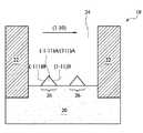
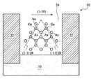
図1は、シリコン基板20(図1で示されず、図2Bと2Cを参照)を含むウェハ10の上視図である。図で示される構造は、ウェハ10のチップの構造も示す。本具体例中、シリコン基板20の表面配向は(001)であるが、他の表面配向を用いることもできる。シャロートレンチアイソレーション(STI)領域22がシリコン基板20中に形成されて、装置領域を定義する。STI領域22により定められるシリコン基板20の一部を窪ませることにより、複数の凹部24(図1、2B、および、2C)が形成される。各凹部24は、長辺(この辺は長さLで示される)と短辺(この辺は幅Wで示される)を有する。幅Wは、長さLより大きくなく、小さい。幅Wはナノレベル、例えば、約50nmより小さいか、或いは、更に、約20nmよりも小さい。一方、長さLは約50nmより大きいが、幅Wに近いか、等しくてもよい。具体例中、ウェハ10(或いは、ウェハ)(上にMOS装置を有する)中の凹部24の長辺の殆ど全部、例えば、90%超は、同じ方向に延伸する。図1の具体例中、凹部24の長辺の殆ど全部ハ、<110>方向と、<110>方向の反対方向である<−1−10>方向に延伸する。注意すべきことは、凹部24の長さLは同じ方向に延伸するが、互いの長さは、等しいか異なることである。凹部24の幅Wも同じ方向に延伸するが、それらの長さも等しいか異なる。 FIG. 1 is a top view of a
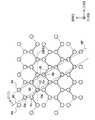
図2Aは、1個の凹部24を含むウェハ10の一部の上視図である。凹部24の短辺は、<1−10>方向と、<1−10>方向の反対方向である<−110>方向に沿って延伸する。凹部24の長辺は、<110>方向と<−1−10>方向に沿って延伸する。その後、ヘテロエピタキシャル成長(hetero-epitaxy)が実行されて、凹部24内のシリコン上で、III−V族化合物半導体材料を成長させる。以下の討論で、III−V族化合物半導体材料は、GaAsを例として、具体例の概念を説明しているが、別のIII−V族化合物半導体材料を形成することもできる。 FIG. 2A is a top view of a part of the
エピタキシーの初期、アイランド26等の臨界超過核(supercritical nuclei)が形成される(凹部24中の方形)。この段階は、核形成段階(nucleation stage)と称される。異なる表面配向上の異なるエネルギーにより、ファセットがアイランド26上に形成され、得られたアイランド26は、ピラミッド状の4個のファセットを有する。ピラミッド型の4個のファセットは、表面配向(1−11)B、(−111)B、(−1−11)A、および、(111)Aを有する。ファセット(1−11)Bと(−111)Bは長辺に面し、ファセット(−1−11)Aと(111)Aは短辺に面する。文字AとBの意義は後続の段落で説明される。 In the initial stage of epitaxy, supercritical nuclei such as
図2Bは、図2Aの構造の断面図で、図2Aの線2B−2Bに沿って得られた断面構造である。ファセット(1−11)Bと(−111)Bは、それぞれ、紙面内向きと紙面から外向きのファセットで、ファセット(−1−11)Aと(111)Aは、それぞれ、左上向きと右上向きのファセットである。 2B is a cross-sectional view of the structure of FIG. 2A and is a cross-sectional structure obtained along
図2Cは、図2Aの構造の断面図で、図2Aの線2C−2Cに沿って得られる断面構造である。ファセットは、図2Cで表示され、図2A中で見つけることができる。 2C is a cross-sectional view of the structure of FIG. 2A and is a cross-sectional structure obtained along
凹部24の幅Wはナノレベルで、図2Cで示されるように、凹部24の短辺は、例えば、約4より小さい、或いは、2個だけナノアイランド26を収容しているが、更に多くのナノアイランドを収容することもできる。エピタキシャル成長の開始で、ナノアイランド26は互いに離される。時間と共に、ナノアイランド26が成長し、徐々に互いに結合して、STI領域22の側壁と接触する。しかし、ナノアイランド26の成長の間、ナノアイランド26が合併されるまで、および/または、STI領域22の側壁に接触するまで、ピラミッド型が維持され、その時、成長は主に垂直方向である。図3は得られたGaAs膜28を示す。 The width W of the
ファセット(図2A−2C)中の文字AとBの意義は、図4と5を用いて説明され、成長GaAsの格子構造を示す。図4の格子構造は、図2Bと同じ角度(図4で表示される方向)から見られる。シリコンとは違って、Ga原子とAs原子等、2個の異なるタイプの原子があるので、GaAsは極性を持つことが観察される。各Ga原子は、4個のAs原子と4個の結合を形成し、各As原子は、4個のGa原子と4個の結合を形成する。線40と40’は、エピタキシャル成長中に形成される可能なファセットを示し、ファセットは、それぞれ、紙面と交差線40と40’に延伸する。ファセットは、左下から右上に成長する。注意すべきことは、ファセット40中、各Ga原子(Ga原子42等)は、アップボンド(up-bond)と称される上向きの1結合(つまり、ナノアイランドから離れる方向)、および、ダウンボンド(down-bond)と称される下向きの3結合(ナノアイランドから離れる方向)を有する。ファセット40’中、各As原子(As原子46等)は、3個のアップボンド48と1個のダウンボンド44を有する。注意すべきことは、図4は断面図なので、2個のアップボンド48だけが見えることである。明細書中、各Ga原子が、1個のアップボンド54(と3個のダウンボンド56)を有し、および、各As原子が、3個のアップボンド(と1個のダウンボンド)を有するファセットは、文字Aで示される。従って、図2Aを参照すると、ファセット(−1−11)Aと(111)Aの後に文字Aを加え、Aファセットと称される。 The significance of letters A and B in the facets (FIGS. 2A-2C) is explained using FIGS. 4 and 5 and shows the lattice structure of the grown GaAs. The lattice structure of FIG. 4 can be seen from the same angle (direction displayed in FIG. 4) as FIG. 2B. Unlike silicon, it is observed that GaAs has polarity because there are two different types of atoms, such as Ga and As atoms. Each Ga atom forms 4 bonds with 4 As atoms, and each As atom forms 4 bonds with 4 Ga atoms.
図5の格子構造は、図2Cの視角と同じである(図5で示される方向を参照する)。線50と50’は、エピタキシャル成長間に形成される可能なファセットを示し、ファセットは、それぞれ、紙面と交差線50と50’に延伸する。ファセットは、左下から右上に成長する。注意すべきことは、ファセット50’、各As原子(As原子52等)は、1個のアップボンドと3個のダウンボンドを有することである。ファセット50の各Ga原子(Ga原子56等)は、3個のアップボンド58と1個のダウンボンド54を有する(図5は断面図で、2個のアップボンド58だけが見える)。各As原子が1個のアップボンド(と3個のダウンボンド)を有し、各Ga原子が3個のアップボンド(と1個のダウンボンド)を有するファセットは文字Bで示される。従って、図2Aを参照すると、ファセット(1−11)Bと(−111)Bは、その後、文字Bが加えられ、以下で、Bファセットと称される。 The lattice structure of FIG. 5 is the same as the viewing angle of FIG. 2C (refer to the direction shown in FIG. 5).
図2Aを参照すると、AファセットとBファセットは、どちらもスタック欠陥や双晶(twins)等の欠陥を有する。AファセットとBファセットの欠陥密度は異なる。Aファセット、或いは、Bファセットが、どちらも、他よりも大きい欠陥密度を有していても、ナノアイランド26の成長状況により影響される。好ましくは、大量の欠陥を有するファセットは、凹部24の長辺に面し、これらのファセットは快速に成長して、STI領域22の側壁と結合し、これらの高欠陥密度ファセットが終了する。ファセットがSTI領域22の側壁と結合後、成長は主に垂直方向になる。欠陥が少ないファセットは短辺に面する。ファセットの方向を制御することにより、高品質のGaAs膜が成長する。 Referring to FIG. 2A, both the A facet and the B facet have defects such as stack defects and twins. The defect density of A facet and B facet is different. Whether the A facet or the B facet has a larger defect density than the others, it is affected by the growth state of the
具体例中、図2Aで示されるように、凹部24の長辺は<110>方向に沿って延伸し、短辺は<1−10>方向に沿って延伸する。従って、Aファセットは、Bファセットより欠陥密度が小さい。これは、例えば、核形成段階で、高基板温度、および/または、低V族元素対III族元素の流量比率を採用することにより達成される。V族元素対III族元素の流量比率は、プロセスガス中、第III族元素と第III族元素の原子数量の比率である。具体例中、GaAsが成長し、V族元素対III族元素の流量比率は、As含有プロセスガス中のAs原子の流量比率対Ga含有プロセスガス中のGa原子の流量比率で、As対Ga流量比率とも称される。具体例中、V族元素対III族元素の比は、約50より小さいか、或いは、約30よりもっと小さい。基板温度は、約400℃より高く、約400℃〜約600℃、或いは、約500℃より高く、例えば、約500℃〜約600℃である。このようなプロセス条件は、As結合の品質を改善し、Aファセットの欠陥は、Bファセットより少ない。この実施例中、Bファセットは高い欠陥密度を有するが、BファセットがSTI領域22の側壁に迅速に結合されて、高密度ファセットが停止される。GaAsの品質全般が改善される。 In the specific example, as shown in FIG. 2A, the long side of the
当然のことながら、上述のV族元素対III族元素の流量比率と基板温度は、核生成段階、つまり、ナノアイランド26がまだピラミッド形状の時に使用される。核形成段階後、V族元素対III族元素の流量比率と核形成段階が相同、或いは、異なるV族元素対III族元素の流量比率下で、GaAs膜28(図3)が継続して形成される。同様に、基板温度と核形成段階が同じ、或いは、異な基板温度下で、GaAs膜28が継続して形成される。 Of course, the flow ratios of the V group element to the III group element and the substrate temperature described above are used in the nucleation stage, that is, when the
GaAs膜28の形成後(図3)、MOS装置30が形成され、図6で示される。MOS装置30のチャネル長さ方向は、凹部24(とGaAs膜28)の長辺方向にある。言い換えると、ゲート電極31は、GaAs膜28の短辺方向に延伸する。従って、エピタキシーGaAs膜28上に形成されるウェハ10中の全MOS装置は、同じ方向に延伸するゲート電極31を有し、GaAs膜28の短辺に平行である。III−V族化合物半導体膜上ではなく、ウェハ10中かシリコン上に、別のMOS装置がある場合、それらのMOS装置のゲート電極は、あらゆる方向に延伸し、例えば、ゲート電極31と平行、或いは、垂直方向等である。更に、MOS装置を有さないダミーGaAs膜等のGaAs膜は、これらのGaAs膜の長辺方向も、あらゆる方向に延伸する。 After the formation of the GaAs film 28 (FIG. 3), a
図7は、別の具体例の上視図である。上視図の具体例は、凹部24の短辺が<110>/<−1−10>方向に延伸し、凹部24の長辺が<1−10>/<−110>方向に延伸する以外は、図1の具体例と類似している。更に、ウェハ10(或いは、同じウェハ中)中の凹部24は、同じ方向に延伸する長辺を有する。 FIG. 7 is a top view of another specific example. In the specific example of the top view, the short side of the
図8Aを参照すると、一凹部24の一部が示される。ヘテロエピタキシーが実行されて、凹部24内のシリコン上に、GaAsを成長させ、ピラミッド型ナノアイランド26(凹部24中の方形)が形成される(図8Bと8Cを参照する)。ピラミッド型の4個のファセットは、表面配向(1−11)B、(−111)B、(−1−11)A、および、(111)Aを有する。ファセット(1−11)Bと(−111)Bは、凹部24の長辺に面し、ファセット(−1−11)Aと(111)Aは凹部24の短辺に面する。 Referring to FIG. 8A, a portion of one
図8Bは、図8Aの構造の断面図で、図8Aの線8B−8Bに沿って得られる断面構造である。ファセット(−1−11)Aと(111)A(図8Bで示されない)は、それぞれ、紙面内向けと紙面外向けのファセットで、ファセット(1−11)Bと(−111)Bは、それぞれ、左上向けと右上向けのファセットである。(1−11)Bと(−111)Bファセットは点線で示され、(1−11)Bと(−111)Bファセットが所在する平面は、紙面を垂直に延伸し、点線を通過する。 FIG. 8B is a cross-sectional view of the structure of FIG. 8A and is a cross-sectional structure obtained along
図8Cは、図8Aの構造の断面図で、図8Aの線8C−8Cの垂直平面に沿って得られる断面構造である。各ファセットは図8C上で表示され、図8A中で見つけられる。 8C is a cross-sectional view of the structure of FIG. 8A and is a cross-sectional structure obtained along the vertical plane of
図7〜図8Cで示される基板20と凹部24の方向により、Bファセットの欠陥密度は、Aファセットより小さい。これは、例えば、低基板温度、および/または、高V族元素対III族元素の流量比率を採用することにより達成される。具体例中、V族元素対III族元素の比は、約30より大きく、或いは、更に、約100より高い。基板温度は約400℃より低く、約200℃〜約400℃間か、或いは、約300℃〜約400℃、或いは、約300℃より低い。このようなプロセス条件により、Bファセット、Aファセットより欠陥が少ない。この場合、Aファセットは高欠陥密度を有するが、Aファセットは、STI領域22の側壁に迅速に結合され、高密度ファセットは停止される。成長GaAs膜の品質全体が改善される。 Due to the direction of the
核形成段階後、GaAs膜の形成が継続される。図9で示されるGaAs膜28の形成後、MOS装置30が形成される。再び、MOS装置30のチャネル長さ方向は凹部24の長辺方向で、エピタキシャルGaAs上に形成される全MOS装置30(同じウェハ中)は、同じ方向に延伸するゲート電極31を有し、凹部24の短辺に平行である。 After the nucleation step, GaAs film formation continues. After the formation of the
具体例は幾つかの長所を有する。同じ方向で、同じチップ/ウェハ上の凹部の長辺を配列させ、長辺の方向に従って、凹部中にGaAsをエピタキシャル成長させるプロセス条件を調整することにより、得られたGaAs膜の欠陥は抑制され、高品質のGaAs膜が成長する。 The example has several advantages. By aligning the long sides of the recesses on the same chip / wafer in the same direction and adjusting the process conditions for epitaxial growth of GaAs in the recesses according to the direction of the long sides, defects in the obtained GaAs film are suppressed, A high quality GaAs film is grown.
本発明では好ましい実施例を前述の通り開示したが、これらは決して本発明に限定するものではなく、当該技術を熟知する者なら誰でも、本発明の精神と領域を脱しない範囲内で各種の変動や潤色を加えることができ、従って本発明の保護範囲は、特許請求の範囲で指定した内容を基準とする。 In the present invention, preferred embodiments have been disclosed as described above. However, the present invention is not limited to the present invention, and any person who is familiar with the technology can use various methods within the spirit and scope of the present invention. Variations and moist colors can be added, so the protection scope of the present invention is based on what is specified in the claims.
10 ウェハ
20 基板
22 シャロートレンチアイソレーション
24 凹部
L 長さ
W 幅
26 アイランド
28 GaAs膜
40、40’、50、50’ 線
42、56 Ga原子
46、52 As原子
44、48、54、56、58 ボンド
A、B ファセット
30 MOS装置
31 ゲート電極10
Claims (10)
Translated fromJapaneseシリコン基板を提供するステップと、
前記シリコン基板中に、複数のシャロートレンチアイソレーション(STI)領域を形成するステップと、
前記複数のSTI領域の両側間の前記シリコン基板の上部分を除去することにより、凹部を形成するステップと、
前記凹部に、III−V族化合物半導体材料をエピタキシャル成長させるステップと、
からなり、
前記シリコン基板中の全凹部の全長辺は同じ方向に延伸することを特徴とする方法。A method for forming an integrated circuit structure comprising:
Providing a silicon substrate;
Forming a plurality of shallow trench isolation (STI) regions in the silicon substrate;
Forming a recess by removing an upper part of the silicon substrate between both sides of the plurality of STI regions;
Epitaxially growing a III-V compound semiconductor material in the recess;
Consists of
A method in which the full length sides of all the recesses in the silicon substrate extend in the same direction.
(001)表面配向のシリコン基板を有するウェハを提供するステップと、
前記シリコン基板中に、複数のシャロートレンチアイソレーション(STI)領域を形成するステップと、
前記複数のSTI領域の両側間の前記シリコン基板の上部分を除去することにより、凹部を形成するステップと、
前記凹部に、GaAs膜をエピタキシャル成長させるステップと、
からなり、
前記ウェハ中の全凹部の全長辺は、前記シリコン基板の<110>方向に延伸し、
前記エピタキシャル成長させるステップの間、As対Gaの流量比率は、約50より低く、前記シリコン基板の温度が約400℃より高いことを特徴とする方法。A method for forming an integrated circuit structure comprising:
Providing a wafer having a (001) surface-oriented silicon substrate;
Forming a plurality of shallow trench isolation (STI) regions in the silicon substrate;
Forming a recess by removing an upper part of the silicon substrate between both sides of the plurality of STI regions;
Epitaxially growing a GaAs film in the recess;
Consists of
The full length side of all the recesses in the wafer extends in the <110> direction of the silicon substrate,
During the epitaxial growth step, the flow rate ratio of As to Ga is lower than about 50, and the temperature of the silicon substrate is higher than about 400 ° C.
Applications Claiming Priority (4)
| Application Number | Priority Date | Filing Date | Title |
|---|---|---|---|
| US24989709P | 2009-10-08 | 2009-10-08 | |
| US61/249,897 | 2009-10-08 | ||
| US12/842,546 | 2010-07-23 | ||
| US12/842,546US9601328B2 (en) | 2009-10-08 | 2010-07-23 | Growing a III-V layer on silicon using aligned nano-scale patterns |
Publications (2)
| Publication Number | Publication Date |
|---|---|
| JP2011082526Atrue JP2011082526A (en) | 2011-04-21 |
| JP5587128B2 JP5587128B2 (en) | 2014-09-10 |
Family
ID=43855168
Family Applications (1)
| Application Number | Title | Priority Date | Filing Date |
|---|---|---|---|
| JP2010228979AActiveJP5587128B2 (en) | 2009-10-08 | 2010-10-08 | Method for growing III-V layers on silicon using oriented nanoscale patterns |
Country Status (5)
| Country | Link |
|---|---|
| US (2) | US9601328B2 (en) |
| JP (1) | JP5587128B2 (en) |
| KR (1) | KR101175004B1 (en) |
| CN (1) | CN102034689B (en) |
| TW (1) | TWI487063B (en) |
Cited By (2)
| Publication number | Priority date | Publication date | Assignee | Title |
|---|---|---|---|---|
| JP2017501562A (en)* | 2013-12-23 | 2017-01-12 | インテル・コーポレーション | Wide bandgap transistor on non-native semiconductor substrate and method of manufacturing the same |
| US10032911B2 (en) | 2013-12-23 | 2018-07-24 | Intel Corporation | Wide band gap transistor on non-native semiconductor substrate |
Families Citing this family (14)
| Publication number | Priority date | Publication date | Assignee | Title |
|---|---|---|---|---|
| US9601328B2 (en) | 2009-10-08 | 2017-03-21 | Taiwan Semiconductor Manufacturing Company, Ltd. | Growing a III-V layer on silicon using aligned nano-scale patterns |
| CN102243994B (en)* | 2011-07-22 | 2013-02-06 | 中国科学院半导体研究所 | Method for growing silicon-based gallium arsenide material with inverted V-shaped silicon dioxide trench structure |
| CN102244007B (en)* | 2011-07-22 | 2012-12-12 | 中国科学院半导体研究所 | Preparation of silicon-based gallium arsenide material by utilizing V-shaped groove |
| CN102263015B (en)* | 2011-07-22 | 2012-11-14 | 中国科学院半导体研究所 | Method for preparing silica-based gallium arsenide material structure applied to n-channel metal oxide semiconductor (nMOS) |
| US9312344B2 (en) | 2013-03-13 | 2016-04-12 | Taiwan Semiconductor Manufacturing Company, Ltd. | Methods for forming semiconductor materials in STI trenches |
| EP2804203A1 (en) | 2013-05-17 | 2014-11-19 | Imec | III-V device and method for manufacturing thereof |
| GB201321949D0 (en) | 2013-12-12 | 2014-01-29 | Ibm | Semiconductor nanowire fabrication |
| US9773889B2 (en)* | 2014-07-18 | 2017-09-26 | Taiwan Semiconductor Manufacturing Company Limited | Method of semiconductor arrangement formation |
| EP3125273B1 (en) | 2015-07-31 | 2024-08-28 | IMEC vzw | Strained group iv channels |
| US9620360B1 (en) | 2015-11-27 | 2017-04-11 | International Business Machines Corporation | Fabrication of semiconductor junctions |
| US9735010B1 (en) | 2016-05-27 | 2017-08-15 | International Business Machines Corporation | Fabrication of semiconductor fin structures |
| US10249492B2 (en) | 2016-05-27 | 2019-04-02 | International Business Machines Corporation | Fabrication of compound semiconductor structures |
| US20190378952A1 (en)* | 2018-06-08 | 2019-12-12 | Alliance For Sustainable Energy, Llc | Enabling low-cost iii-v/si integration through nucleation of gap on v-grooved si substrates |
| CN110534409B (en)* | 2019-08-02 | 2022-07-29 | 中国科学院微电子研究所 | A method for epitaxial GaAs on a silicon substrate and a semiconductor device prepared therefrom |
Citations (7)
| Publication number | Priority date | Publication date | Assignee | Title |
|---|---|---|---|---|
| JPH0267723A (en)* | 1988-09-01 | 1990-03-07 | Seiko Epson Corp | Method for manufacturing compound semiconductor thin film |
| JPH0517278A (en)* | 1991-07-05 | 1993-01-26 | Asahi Glass Co Ltd | Compound semiconductor crystal manufacturing method and manufacturing apparatus |
| JP2002026143A (en)* | 2000-04-27 | 2002-01-25 | Internatl Business Mach Corp <Ibm> | Method of forming oxide layer on trench sidewall |
| JP2003037061A (en)* | 2001-07-24 | 2003-02-07 | Sharp Corp | Semiconductor thin film, method for forming the same, and semiconductor device |
| JP2003158074A (en)* | 2002-07-02 | 2003-05-30 | Matsushita Electric Ind Co Ltd | Semiconductor multilayer substrate and method of manufacturing semiconductor multilayer film |
| WO2006125040A2 (en)* | 2005-05-17 | 2006-11-23 | Amberwave Systems Corporation | Lattice-mismatched semiconductor structures with reduced dislocation defect densities related methods for device fabrication |
| JP2009503871A (en)* | 2005-07-26 | 2009-01-29 | アンバーウェーブ システムズ コーポレイション | Solutions for the integration of alternative active area materials into integrated circuits |
Family Cites Families (12)
| Publication number | Priority date | Publication date | Assignee | Title |
|---|---|---|---|---|
| US6348096B1 (en)* | 1997-03-13 | 2002-02-19 | Nec Corporation | Method for manufacturing group III-V compound semiconductors |
| JP2001338988A (en)* | 2000-05-25 | 2001-12-07 | Hitachi Ltd | Semiconductor device and manufacturing method thereof |
| JP4865166B2 (en)* | 2001-08-30 | 2012-02-01 | 新電元工業株式会社 | Transistor manufacturing method, diode manufacturing method |
| WO2007112066A2 (en) | 2006-03-24 | 2007-10-04 | Amberwave Systems Corporation | Lattice-mismatched semiconductor structures and related methods for device fabrication |
| US7803690B2 (en)* | 2006-06-23 | 2010-09-28 | Taiwan Semiconductor Manufacturing Company, Ltd. | Epitaxy silicon on insulator (ESOI) |
| US8173551B2 (en)* | 2006-09-07 | 2012-05-08 | Taiwan Semiconductor Manufacturing Co., Ltd. | Defect reduction using aspect ratio trapping |
| WO2008039534A2 (en) | 2006-09-27 | 2008-04-03 | Amberwave Systems Corporation | Quantum tunneling devices and circuits with lattice- mismatched semiconductor structures |
| WO2008039495A1 (en) | 2006-09-27 | 2008-04-03 | Amberwave Systems Corporation | Tri-gate field-effect transistors formed by aspect ratio trapping |
| US7808082B2 (en) | 2006-11-14 | 2010-10-05 | International Business Machines Corporation | Structure and method for dual surface orientations for CMOS transistors |
| CN101420001B (en)* | 2007-10-22 | 2012-02-22 | 泰谷光电科技股份有限公司 | Method of Self-bonding Epitaxy |
| US7645624B2 (en)* | 2007-10-31 | 2010-01-12 | Tekcore Co., Ltd. | Method for self bonding epitaxy |
| US9601328B2 (en) | 2009-10-08 | 2017-03-21 | Taiwan Semiconductor Manufacturing Company, Ltd. | Growing a III-V layer on silicon using aligned nano-scale patterns |
- 2010
- 2010-07-23USUS12/842,546patent/US9601328B2/ennot_activeExpired - Fee Related
- 2010-09-17KRKR1020100091780Apatent/KR101175004B1/enactiveActive
- 2010-10-04TWTW099133662Apatent/TWI487063B/enactive
- 2010-10-08CNCN2010105128535Apatent/CN102034689B/ennot_activeExpired - Fee Related
- 2010-10-08JPJP2010228979Apatent/JP5587128B2/enactiveActive
- 2017
- 2017-03-20USUS15/463,047patent/US10020189B2/enactiveActive
Patent Citations (8)
| Publication number | Priority date | Publication date | Assignee | Title |
|---|---|---|---|---|
| JPH0267723A (en)* | 1988-09-01 | 1990-03-07 | Seiko Epson Corp | Method for manufacturing compound semiconductor thin film |
| JPH0517278A (en)* | 1991-07-05 | 1993-01-26 | Asahi Glass Co Ltd | Compound semiconductor crystal manufacturing method and manufacturing apparatus |
| JP2002026143A (en)* | 2000-04-27 | 2002-01-25 | Internatl Business Mach Corp <Ibm> | Method of forming oxide layer on trench sidewall |
| JP2003037061A (en)* | 2001-07-24 | 2003-02-07 | Sharp Corp | Semiconductor thin film, method for forming the same, and semiconductor device |
| JP2003158074A (en)* | 2002-07-02 | 2003-05-30 | Matsushita Electric Ind Co Ltd | Semiconductor multilayer substrate and method of manufacturing semiconductor multilayer film |
| WO2006125040A2 (en)* | 2005-05-17 | 2006-11-23 | Amberwave Systems Corporation | Lattice-mismatched semiconductor structures with reduced dislocation defect densities related methods for device fabrication |
| JP2008546181A (en)* | 2005-05-17 | 2008-12-18 | アンバーウェーブ システムズ コーポレイション | Lattice-mismatched semiconductor structure with low dislocation defect density and related device manufacturing method |
| JP2009503871A (en)* | 2005-07-26 | 2009-01-29 | アンバーウェーブ システムズ コーポレイション | Solutions for the integration of alternative active area materials into integrated circuits |
Cited By (3)
| Publication number | Priority date | Publication date | Assignee | Title |
|---|---|---|---|---|
| JP2017501562A (en)* | 2013-12-23 | 2017-01-12 | インテル・コーポレーション | Wide bandgap transistor on non-native semiconductor substrate and method of manufacturing the same |
| US10032911B2 (en) | 2013-12-23 | 2018-07-24 | Intel Corporation | Wide band gap transistor on non-native semiconductor substrate |
| US10580895B2 (en) | 2013-12-23 | 2020-03-03 | Intel Corporation | Wide band gap transistors on non-native semiconductor substrates |
Also Published As
| Publication number | Publication date |
|---|---|
| TW201113975A (en) | 2011-04-16 |
| TWI487063B (en) | 2015-06-01 |
| US20110086491A1 (en) | 2011-04-14 |
| CN102034689A (en) | 2011-04-27 |
| US20170194141A1 (en) | 2017-07-06 |
| KR20110038578A (en) | 2011-04-14 |
| US10020189B2 (en) | 2018-07-10 |
| JP5587128B2 (en) | 2014-09-10 |
| KR101175004B1 (en) | 2012-08-17 |
| CN102034689B (en) | 2013-06-05 |
| US9601328B2 (en) | 2017-03-21 |
Similar Documents
| Publication | Publication Date | Title |
|---|---|---|
| JP5587128B2 (en) | Method for growing III-V layers on silicon using oriented nanoscale patterns | |
| US11251272B2 (en) | Lattice-mismatched semiconductor structures with reduced dislocation defect densities and related methods for device fabrication | |
| EP2595176B1 (en) | Lattice-mismatched semiconductor structures with reduced dislocation defect densities and related methods for device fabrication | |
| US20070267722A1 (en) | Lattice-mismatched semiconductor structures with reduced dislocation defect densities and related methods for device fabrication | |
| US20160111285A1 (en) | Lattice-mismatched semiconductor structures with reduced dislocation defect densities and related methods for device fabrication | |
| US20030102469A1 (en) | Semiconductor device and method therefor | |
| JP2005072582A (en) | Strained channel FinFET with uniform channel thickness and isolation gate | |
| CN104051267A (en) | Method of forming semiconductor material in STI trench | |
| CN102024768A (en) | Semiconductor device and method for manufacturing semiconductor structure | |
| JP2011066414A (en) | High-quality hetero-epitaxy by using nano-scale epitaxy technology | |
| CN102280469B (en) | Epitaxial growth of III-V compound semiconductors on silicon surfaces | |
| US9859397B2 (en) | Growing groups III-V lateral nanowire channels | |
| JP2018509362A (en) | Semiconductor wafer with single crystal IIIA nitride layer | |
| US7235809B2 (en) | Semiconductor channel on insulator structure | |
| TWI237908B (en) | A method for manufacturing a strained Si having few threading dislocations | |
| TWI257690B (en) | Semiconductor device having a smooth EPI layer and a method for its manufacture | |
| KR101345897B1 (en) | A semiconductor device comprising a honeycomb heteroepitaxy | |
| JP2003197905A (en) | Semiconductor substrate and field effect transistor and their fabricating method |
Legal Events
| Date | Code | Title | Description |
|---|---|---|---|
| A977 | Report on retrieval | Free format text:JAPANESE INTERMEDIATE CODE: A971007 Effective date:20130311 | |
| A131 | Notification of reasons for refusal | Free format text:JAPANESE INTERMEDIATE CODE: A131 Effective date:20130319 | |
| A521 | Request for written amendment filed | Free format text:JAPANESE INTERMEDIATE CODE: A523 Effective date:20130612 | |
| A131 | Notification of reasons for refusal | Free format text:JAPANESE INTERMEDIATE CODE: A131 Effective date:20131126 | |
| A521 | Request for written amendment filed | Free format text:JAPANESE INTERMEDIATE CODE: A523 Effective date:20140224 | |
| TRDD | Decision of grant or rejection written | ||
| A01 | Written decision to grant a patent or to grant a registration (utility model) | Free format text:JAPANESE INTERMEDIATE CODE: A01 Effective date:20140701 | |
| A61 | First payment of annual fees (during grant procedure) | Free format text:JAPANESE INTERMEDIATE CODE: A61 Effective date:20140723 | |
| R150 | Certificate of patent or registration of utility model | Ref document number:5587128 Country of ref document:JP Free format text:JAPANESE INTERMEDIATE CODE: R150 | |
| R250 | Receipt of annual fees | Free format text:JAPANESE INTERMEDIATE CODE: R250 | |
| R250 | Receipt of annual fees | Free format text:JAPANESE INTERMEDIATE CODE: R250 | |
| R250 | Receipt of annual fees | Free format text:JAPANESE INTERMEDIATE CODE: R250 | |
| R250 | Receipt of annual fees | Free format text:JAPANESE INTERMEDIATE CODE: R250 | |
| R250 | Receipt of annual fees | Free format text:JAPANESE INTERMEDIATE CODE: R250 | |
| R250 | Receipt of annual fees | Free format text:JAPANESE INTERMEDIATE CODE: R250 | |
| R250 | Receipt of annual fees | Free format text:JAPANESE INTERMEDIATE CODE: R250 | |
| R250 | Receipt of annual fees | Free format text:JAPANESE INTERMEDIATE CODE: R250 | |
| R250 | Receipt of annual fees | Free format text:JAPANESE INTERMEDIATE CODE: R250 |