JP2011077578A - Tuner module - Google Patents
Tuner moduleDownload PDFInfo
- Publication number
- JP2011077578A JP2011077578AJP2009223791AJP2009223791AJP2011077578AJP 2011077578 AJP2011077578 AJP 2011077578AJP 2009223791 AJP2009223791 AJP 2009223791AJP 2009223791 AJP2009223791 AJP 2009223791AJP 2011077578 AJP2011077578 AJP 2011077578A
- Authority
- JP
- Japan
- Prior art keywords
- electronic component
- conductive sheet
- tuner module
- heat conductive
- slit
- Prior art date
- Legal status (The legal status is an assumption and is not a legal conclusion. Google has not performed a legal analysis and makes no representation as to the accuracy of the status listed.)
- Pending
Links
Images


Classifications
- H—ELECTRICITY
- H05—ELECTRIC TECHNIQUES NOT OTHERWISE PROVIDED FOR
- H05K—PRINTED CIRCUITS; CASINGS OR CONSTRUCTIONAL DETAILS OF ELECTRIC APPARATUS; MANUFACTURE OF ASSEMBLAGES OF ELECTRICAL COMPONENTS
- H05K7/00—Constructional details common to different types of electric apparatus
- H05K7/20—Modifications to facilitate cooling, ventilating, or heating
- H05K7/2039—Modifications to facilitate cooling, ventilating, or heating characterised by the heat transfer by conduction from the heat generating element to a dissipating body
- H05K7/20436—Inner thermal coupling elements in heat dissipating housings, e.g. protrusions or depressions integrally formed in the housing
- H05K7/20445—Inner thermal coupling elements in heat dissipating housings, e.g. protrusions or depressions integrally formed in the housing the coupling element being an additional piece, e.g. thermal standoff
- H05K7/20472—Sheet interfaces
Landscapes
- Physics & Mathematics (AREA)
- Thermal Sciences (AREA)
- Engineering & Computer Science (AREA)
- Microelectronics & Electronic Packaging (AREA)
- Structure Of Receivers (AREA)
Abstract
Description
Translated fromJapanese本発明は、ラジオ受信機用のチューナモジュールに関し、特に、人工衛星からの電波(以下「衛星波」とも呼ぶ)または地上での電波(以下「地上波」とも呼ぶ)を受信してデジタルラジオ放送を聴取することが可能な車載用デジタルラジオ受信機に適したチューナモジュールに関する。 The present invention relates to a tuner module for a radio receiver, and more particularly, to receive a radio wave from an artificial satellite (hereinafter also referred to as “satellite wave”) or a radio wave on the ground (hereinafter also referred to as “terrestrial wave”). The present invention relates to a tuner module suitable for a vehicle-mounted digital radio receiver capable of listening to the sound.
SDARS(Satellite Digital Audio Radio Service)とは、米国における衛星(以下、「SDARS衛星」と呼ぶ)を使用したデジタル放送によるサービスである。すなわち、米国においては、SDARS衛星からの衛星波または地上波を受信して、デジタルラジオ放送を聴取可能にしたデジタルラジオ受信機が開発され、実用化されている。現在、米国では、XMとシリウスという2つの放送局が計250チャネル以上のラジオ番組を全国に提供している。このデジタルラジオ受信機は、一般には、自動車等の移動体(移動局)に搭載され、周波数が約2.3GHz帯の電波(SDARS信号)を受信してラジオ放送を聴取することが可能である。すなわち、デジタルラジオ受信機は、モバイル放送を聴取することが可能なラジオ受信機である。受信電波(SDARS信号)の周波数が約2.3GHz帯なので、そのときの受信波長(共振波長)λは約128mmである。尚、地上波は、衛星波を一旦、地球局で受信した後、周波数を若干シフトし、直線偏波で再送信したものである。すなわち、衛星波は円偏波であるのに対して、地上波は直線偏波である。SDARS用アンテナとして、パッチアンテナのような平面アンテナが使用される。 SDARS (Satellite Digital Audio Radio Service) is a service by digital broadcasting using a satellite in the United States (hereinafter referred to as “SDARS satellite”). That is, in the United States, digital radio receivers that receive satellite waves or terrestrial waves from SDARS satellites and can listen to digital radio broadcasts have been developed and put into practical use. Currently, in the United States, two broadcasting stations, XM and Sirius, provide a total of over 250 channels of radio programs nationwide. This digital radio receiver is generally mounted on a mobile body (mobile station) such as an automobile, and can receive radio waves by receiving radio waves (SDARS signals) having a frequency of about 2.3 GHz band. . That is, the digital radio receiver is a radio receiver capable of listening to mobile broadcasts. Since the frequency of the reception radio wave (SDARS signal) is about 2.3 GHz band, the reception wavelength (resonance wavelength) λ at that time is about 128 mm. The terrestrial wave is a satellite wave that is once received by the earth station, then slightly shifted in frequency, and retransmitted with linearly polarized waves. That is, satellite waves are circularly polarized while terrestrial waves are linearly polarized. A planar antenna such as a patch antenna is used as the SDARS antenna.
XM衛星ラジオ用アンテナ装置は、静止衛星2基より円偏波電波を受信し、不感地帯では地上直線偏波設備により電波を受信する。一方、シリウス衛星ラジオ用アンテナ装置は、周回衛星3基(シンクロ型)より円偏波電波を受信し、不感地帯では地上直線偏波設備により電波を受信する。 The antenna device for XM satellite radio receives circularly polarized radio waves from two geostationary satellites, and receives radio waves from the ground linear polarization equipment in the dead zone. On the other hand, the antenna device for Sirius satellite radio receives circularly polarized radio waves from three orbiting satellites (synchronous type), and receives radio waves by the ground linear polarization equipment in the dead zone.
このようにデジタルラジオ放送では、約2.3GHz帯の周波数の電波(SDARS信号)が使用されるので、そのSDARS信号を受信するアンテナ装置は、室外に設置される場合が多い。従って、デジタルラジオ受信機を自動車等の移動体(移動局)に搭載するには、そのアンテナ装置を移動体(移動局)の屋根に取り付けられる場合が多い。 As described above, since radio waves (SDARS signals) having a frequency of about 2.3 GHz band are used in digital radio broadcasting, an antenna device that receives the SDARS signals is often installed outdoors. Therefore, in order to mount a digital radio receiver on a mobile body (mobile station) such as an automobile, the antenna device is often attached to the roof of the mobile body (mobile station).
このような自動車用アンテナと自動車の室内に設置される受信機本体(ヘッドユニット)とは、延長ケーブルを介して電気的に接続される。ヘッドユニットは外部機器として動作する。 Such an automobile antenna and a receiver main body (head unit) installed in the interior of the automobile are electrically connected via an extension cable. The head unit operates as an external device.
この種の衛星波または地上波を受信する受信システムは、アンテナ部(アンテナ装置)とチューナ部(衛星ラジオ受信モジュール)とを含む。アンテナ部(アンテナ装置)は衛星波または地上波を受信して高周波の受信信号を出力する。チューナ部(衛星ラジオ受信モジュール)は受信信号を復調して音声信号を出力する。 A reception system for receiving this type of satellite wave or terrestrial wave includes an antenna unit (antenna device) and a tuner unit (satellite radio reception module). The antenna unit (antenna device) receives a satellite wave or a ground wave and outputs a high-frequency reception signal. The tuner (satellite radio reception module) demodulates the received signal and outputs an audio signal.
このようなチューナを構成する電子部品は、通常、プリント配線基板に実装されてシールドを兼ねる金属ケースに収容される(例えば、特許文献1参照)。 The electronic components constituting such a tuner are usually mounted on a printed wiring board and housed in a metal case that also serves as a shield (see, for example, Patent Document 1).
図5を参照して、衛星デジタル受信モジュールの構成の一例について説明する。衛星デジタルラジオ受信モジュールは、アンテナ101、チューナ部102、信号復調部103、チャンネル復調部104、音声デコーダ105、データデコータ106、制御部107、および操作部108を有する(例えば、特許文献2参照)。 An example of the configuration of the satellite digital reception module will be described with reference to FIG. The satellite digital radio reception module includes an
ところで、チューナを構成する電子部品にはIC部品も含まれており、このIC部品から熱が発生する。IC部品で発生した熱を良好に外部へ放熱させるために、電子部品(IC部品)と金属ケースとの間に熱伝導シート(伝熱シート)を配置したチューナモジュールが提案されている(例えば、特許文献3参照)。このような熱伝導シート(伝熱シート)としては、例えば、熱伝導性の良好なシリコーンゴムが使用される。 By the way, the electronic components constituting the tuner include IC components, and heat is generated from the IC components. In order to dissipate the heat generated in the IC component to the outside satisfactorily, a tuner module in which a heat conductive sheet (heat transfer sheet) is arranged between the electronic component (IC component) and the metal case has been proposed (for example, (See Patent Document 3). As such a heat conductive sheet (heat transfer sheet), for example, silicone rubber having good heat conductivity is used.
一方、熱伝導シート(伝熱シート)の貼り忘れを確認(防止)するために、金属ケースに覗き穴を設けることが行われている。例えば、特許文献4は、伝熱シートを放熱部材に装着する際の位置ずれを抑えると共に、伝熱シートの有無を容易に確認することができる表示装置を開示している。特許文献4では、その実施例として、伝熱シートの少なくとも対角に対応した放熱部材の箇所に貫通部として丸穴を設けている。 On the other hand, in order to confirm (prevent) forgetting to attach the heat conductive sheet (heat transfer sheet), a peep hole is provided in the metal case. For example, Patent Document 4 discloses a display device that can suppress a positional shift when a heat transfer sheet is attached to a heat radiating member and can easily check the presence or absence of the heat transfer sheet. In Patent Document 4, as an example, a round hole is provided as a penetrating portion in a portion of the heat dissipation member corresponding to at least the diagonal of the heat transfer sheet.
前述したように、熱伝導シート(伝熱シート)としては、熱伝導性の良好なシリコーンゴムが使用される。一方、電子部品(IC部品)と金属ケースとの間に熱伝導シート(伝熱シート)を配置する場合、熱伝導シート(伝熱シート)は、金属ケースと電子部品(IC部品)とで押圧された状態で挟まれる。シリコーンゴムは弾性体であるので、上記押圧によって熱伝導シート(伝熱シート)は伸びることになる。 As described above, a silicone rubber having a good thermal conductivity is used as the thermal conductive sheet (heat transfer sheet). On the other hand, when a heat conductive sheet (heat transfer sheet) is disposed between an electronic component (IC component) and a metal case, the heat conductive sheet (heat transfer sheet) is pressed between the metal case and the electronic component (IC component). It is pinched in the state that was done. Since the silicone rubber is an elastic body, the heat conductive sheet (heat transfer sheet) is stretched by the pressing.
その結果、上記特許文献4に記載されているように、熱伝導シート(伝熱シート)の少なくとも対角に対応した、金属ケース箇所に貫通部(丸穴)を設けた場合、その貫通部(丸穴)から熱伝導シート(伝熱シート)が盛り上がってくる恐れがある。 As a result, as described in Patent Document 4, when a through part (round hole) is provided in the metal case portion corresponding to at least the diagonal of the heat conductive sheet (heat transfer sheet), the through part ( There is a risk that the heat conductive sheet (heat transfer sheet) rises from the round hole.
したがって、本発明の課題は、熱伝導シートの盛上りを防止すると共に、熱伝導シートの有無を容易に確認することができる、チューナモジュールを提供することある。 Therefore, the subject of this invention is providing the tuner module which can confirm the presence or absence of a heat conductive sheet while preventing the rise of a heat conductive sheet.
本発明の他の課題は、熱伝導シートを金属ケースに貼り付ける際の位置ずれを抑えることができる、チューナモジュールを提供することにある。 Another object of the present invention is to provide a tuner module that can suppress displacement when a heat conductive sheet is attached to a metal case.
本発明によれば、回路基板(20)と、アンテナ装置で受信された高周波の受信信号を復調して音声信号を出力するために、前記回路基板上に実装された電子部品(22)と、前記回路基板と前記電子部品とを収納する金属ケース(10)と、前記電子部品と前記金属ケースとの間に配置された熱伝導シート(32)とを有するチューナモジュール(100)であって、前記熱伝導シート(32)は、前記電子部品(22)の外形と実質的に等しいか僅かに小さい寸法を持ち、前記金属ケース(10)には、前記電子部品の外周形状に沿うように、少なくとも1つのスリット状穴(111)が形成されていることを特徴とするチューナモジュールが得られる。 According to the present invention, in order to demodulate a high frequency received signal received by the antenna device and output an audio signal by the circuit board (20), an electronic component (22) mounted on the circuit board, A tuner module (100) having a metal case (10) for housing the circuit board and the electronic component, and a heat conductive sheet (32) disposed between the electronic component and the metal case, The heat conductive sheet (32) has a dimension substantially equal to or slightly smaller than the outer shape of the electronic component (22), and the metal case (10) has an outer peripheral shape of the electronic component, A tuner module characterized in that at least one slit-like hole (111) is formed.
上記チューナモジュールにおいて、前記スリット状穴(111)が互いに対向する位置に、少なくとも2つ形成されていることが望ましい。前記電子部品(22)は、直方体形状をしていてよい。この場合、前記スリット状穴(111)は、前記電子部品(22)の角部と対応する位置に配置されていることが好ましい。前記スリット状穴(111)の数は、4であってよい。各スリット状穴(111)がL字形状をしていることが望ましい。前記熱伝導シート(32)はシリコーンゴムから成ることが好ましい。 In the tuner module, it is desirable that at least two slit-shaped holes (111) are formed at positions facing each other. The electronic component (22) may have a rectangular parallelepiped shape. In this case, it is preferable that the slit-shaped hole (111) is disposed at a position corresponding to the corner of the electronic component (22). The number of the slit holes (111) may be four. It is desirable that each slit-like hole (111) has an L shape. The heat conductive sheet (32) is preferably made of silicone rubber.
尚、上記括弧内の符号は、本発明の理解を容易にするために付したものであり、一例にすぎず、これらに限定されないのは勿論である。 In addition, the code | symbol in the said parenthesis is attached | subjected in order to make an understanding of this invention easy, and it is only an example, and of course is not limited to these.
本発明では、電子部品と金属ケースとの間に配置された熱伝導シートが、電子部品の外形と実質的に等しいか僅かに小さい寸法を持ち、金属ケースに、電子部品の外周形状に沿うように、少なくとも1つのスリット状穴を形成したので、熱伝導シートの盛上りを防止すると共に、熱伝導シートの有無を容易に確認することができる。 In the present invention, the heat conductive sheet disposed between the electronic component and the metal case has a dimension that is substantially equal to or slightly smaller than the outer shape of the electronic component so that the metal case follows the outer peripheral shape of the electronic component. Furthermore, since at least one slit-shaped hole is formed, it is possible to prevent the heat conductive sheet from rising and easily check the presence or absence of the heat conductive sheet.
以下、図面を参照して、本発明の実施の形態について詳細に説明する。 Hereinafter, embodiments of the present invention will be described in detail with reference to the drawings.
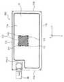
図1乃至図3を参照して、本発明の一実施の形態に係るチューナモジュール100について説明する。図1はチューナモジュール100の平面図である。図2はチューナモジュール100の正面断面図である。図3は図2の主要部を拡大して示すチューナモジュール100の要部拡大断面図である。 A
ここでは、図1及び図2に示されるように、直交座標系(X,Y,Z)を使用している。図1及び図2に示した状態では、X軸方向は前後方向(奥行き方向)であり、Y軸方向は左右方向(横方向)であり、Z軸方向は上下方向(高さ方向)である。 Here, as shown in FIGS. 1 and 2, an orthogonal coordinate system (X, Y, Z) is used. In the state shown in FIGS. 1 and 2, the X-axis direction is the front-rear direction (depth direction), the Y-axis direction is the left-right direction (lateral direction), and the Z-axis direction is the up-down direction (height direction). .
図示のチューナモジュール100は、カーステレオのメイン基板の主面上に横型に設置される(伏せ形取り付けの)例を示している。しかしながら、本発明は、チューナモジュールをカーステレオのメイン基板の主面上に縦型に設置される(縦形取り付けの)場合にも適用可能なのは勿論である。 The illustrated
車載用デジタルラジオ受信機の構成要素のうち、チューナ部と復調部、音声デコーダ部、データデコーダ部およびこれらを制御するコントローラが1つのプリント配線基板(回路基板)20に実装され、このプリント配線基板(回路基板)20が金属ケース(後述する)に収容される場合について示している。このような構成をここでは「チューナモジュール」と呼ぶ。 Among the components of the in-vehicle digital radio receiver, a tuner unit, a demodulator unit, an audio decoder unit, a data decoder unit, and a controller for controlling them are mounted on one printed wiring board (circuit board) 20, and this printed wiring board. The case where (circuit board) 20 is accommodated in a metal case (described later) is shown. Such a configuration is referred to herein as a “tuner module”.
チューナモジュール100は、後述する金属ケース(板金ケース;シールドケース)10とプリント配線基板(回路基板)20とを有する。金属ケース(板金ケース;シールドケース)10は、第1のケース11及び第2のケース12から成る。チューナモジュール100は、をカーステレオの水平方向に延在するメイン基板の主面上に横置きで設置されるタイプなので、第1のケース11はアッパーケースと呼ばれ、第2のケース12はロアーケースと呼ばれる。 The
尚、チューナモジュール100が縦置きの場合、第1のケース11はフロントケースとして、第2のケース12はリアケースとして、それぞれ用いられる。 When the
図示の例では、アッパーケース11、ロアーケース12とも、金属板の折り曲げによって作られる。 In the illustrated example, both the
アッパーケース11は、実質的に底板部(下板部)が無い箱型をしている。すなわち、アッパーケース11は、実質的に前後方向Xおよび左右方向Yで規定されるX−Y平面と平行に延在する上板部11aを持つ。アッパーケース11は、互いに前後方向Xで対向する前板部11bおよび後板部(背板部)11cと、互いに左右方向Yで対向する右板部11dおよび左板部11eとを持つ。 The
一方、ロアーケース12は、実質的に上板部が無い箱型をしている。すなわち、ロアーケース12は、実質的に前後方向Xおよび左右方向Yで規定されるX−Y平面と平行に延在する底板部(下板部)12aを持つ。ロアーケース12は、互いに前後方向Xで対向する前板部(図示せず)および後板部(図示せず)と、互いに左右方向Yで対向する右板部12dおよび左板部12eとを持つ。 On the other hand, the
プリント配線基板(回路基板)20は、外部との電気的接続が必要な部分(後述する)を除いて、アッパーケース11とロアーケース12との間の空間に収容され、シールドが実現される。図示の例では、図2に示されるように、プリント配線基板(回路基板)20は、ロアーケース12に挟まれた状態で固定されている。 The printed wiring board (circuit board) 20 is accommodated in a space between the
図4は、チューナモジュール100を構成している回路部品(電子部品)を実装しているプリント配線基板(回路基板)20を示す図である。図4において、(a)はプリント配線基板(回路基板)20を上面側から見た平面図であり、(b)はプリント配線基板(回路基板)20を下面側から見た底面図である。 FIG. 4 is a diagram showing a printed wiring board (circuit board) 20 on which circuit parts (electronic parts) constituting the
プリント配線基板(回路基板)20は、前後方向Xおよび左右方向Yで規定されるX−Y平面と平行に延在する略矩形の平板状をしている。プリント配線基板(回路基板)20は、互いに上下方向Zで対向する上面20aおよび下面(底面)20bを持つ。プリント配線基板(回路基板)20は、互いに左右方向Yで対向する右辺20cおよび左辺20dと、互いに前後方向Xで対向する前辺20eおよび後辺(背辺)20fを持つ。プリント配線基板(回路基板)20の上面20a側にアッパーケース11が配置され、下面(底面)20b側にロアーケース12が配置されている。 The printed wiring board (circuit board) 20 has a substantially rectangular flat plate shape extending in parallel with the XY plane defined by the front-rear direction X and the left-right direction Y. The printed wiring board (circuit board) 20 has an
図4(a)に示されるように、プリント配線基板(回路基板)20の上面20aには、チューナ部の主要構成部品である第1のIC部品21及び復調部の主要構成部品である第2のIC部品22が実装されている。一方、図4(b)に示されるように、プリント配線基板(回路基板)20の下面(底面)20bには、メモリの主要構成部品である第3のIC部品23が実装されている。 As shown in FIG. 4A, on the
すなわち、プリント配線基板(回路基板)20には、アンテナ装置(図示せず)で受信された高周波の受信信号を復調して音声信号を出力するための電子部品として、第1乃至第3のIC部品21〜23が実装されている。第2のIC部品22は、図4(a)から明らかなように、直方体形状をしている。第3のIC部品23も、図4(b)から明らかなように、直方体形状をしている。 That is, the printed wiring board (circuit board) 20 includes first to third ICs as electronic components for demodulating a high-frequency received signal received by an antenna device (not shown) and outputting an audio signal.
図2および図3に示されるように、第2のIC部品22の上面(ここでは全面)、あるいはこれに対応する金属ケース10の内面(アッパーケース11の上板部11aの内壁)に熱伝導シート32を貼着している。熱伝導シート32は、熱伝導を良くするために第2のIC部品22とアッパーケース11の上板部11aの内壁とに面接触により密着させるようにしている。熱伝導シート32の材料としては、例えばシリコーンゴム、アクリルゴム、黒鉛等が挙げられる。 As shown in FIGS. 2 and 3, heat conduction to the upper surface (here, the entire surface) of the
図示はしないが、第3のIC部品23の上面(ここでは全面)、あるいはこれに対応する金属ケース10の内面(ロアーケース12の底板部12aの内壁)に熱伝導シートを貼着している。 Although not shown, a heat conductive sheet is attached to the upper surface (here, the entire surface) of the
尚、図2および図3は、熱伝導シート32が、金属ケース10(アッパーケース11)と第2のIC部品(電子部品)22とで押圧されて挟まれた状態を示している。従って、図2および図3の状態では、上記押圧によって熱伝導シート32が伸びている。 2 and 3 show a state in which the heat
この押圧前の状態においては、熱伝導シート32は、第2のIC部品(電子部品)22の外形と実質的に等しいか僅かに小さい寸法を持っていることに注意されたい。 It should be noted that the heat
第3のIC部品23の上面に貼着されている熱伝導シート(図示せず)も、押圧前の状態においては、第3のIC部品(電子部品)23の外形と実質的に等しいか僅かに小さい寸法を持っていることに注意されたい。 The heat conductive sheet (not shown) attached to the upper surface of the
図2に示されるように、プリント配線基板(回路基板)20の下面(底面)20bには、その後辺(背辺)20f側に、メイン基板(図示せず)の配線パターンに対して差し込まれるコネクタピン25が取り付けられる。ロアーケース12の底板部(下板部)12aは、このコネクタピン25の設置位置と対応する背板部の位置に、矩形のコネクタ用切欠き部12a−1を持つ。 As shown in FIG. 2, the lower surface (bottom surface) 20b of the printed wiring board (circuit board) 20 is inserted into the wiring pattern of the main board (not shown) on the rear side (back side) 20f side.
また、図4(a)に示されるように、プリント配線基板(回路基板)20は、左奥角部に、アンテナ装置(図示せず)からの高周波(RF)の受信信号を入力するためのRF入力部201を持つ。一方、図2に示されるように、アッパーケース11の上板部11aは、このRF入力部201と対応する左板部11eの位置に、矩形の切欠き部11a−1を持つ。RF入力部201には、RFコネクタ30が接続される。 Also, as shown in FIG. 4A, the printed wiring board (circuit board) 20 is used for inputting a high frequency (RF) reception signal from an antenna device (not shown) to the left back corner. An RF input unit 201 is provided. On the other hand, as shown in FIG. 2, the
RFコネクタ30は、チューナモジュール100の左下方(すなわち、左板部11eに近接した位置)で、左方向に突出した状態で、チューナモジュール100に取り付けられている。 The
図1に示されるように、金属ケース10のアッパーケース11の上板部11aには、第2のIC部品(電子部品)22の外形形状に沿うように、4つのスリット状穴111が形成されている。4つのスリット状穴111は、第2のIC部品(電子部品)22の角部と対応する位置に、4つのスリット状穴111によって囲まれる領域112が第2のIC部品(電子部品)22とほぼ同じとなるように配置されている。各スリット状穴111はL字形状をしている。 As shown in FIG. 1, four slit-shaped
換言すれば、図3に示されるように、熱伝導シート32の反発力を、プリント配線基板(回路基板)20に搭載している第2のIC部品(電子部品)22の外周部へ分散させるように、第2のIC部品(電子部品)22の外周形状に沿って、L字形状の4つのスリット状穴111を金属ケース10(アッパーケース11)に形成している。これにより、図3に示されるように、熱伝導シート32の反発力が矢印方向へ分散する。 In other words, as shown in FIG. 3, the repulsive force of the heat
このように、本実施の形態では、金属ケース10に、電子部品22の外形形状に沿うように、L字形状の4つのスリット状穴111を形成し、4つのスリット状穴111で囲まれる領域112が第2のIC部品(電子部品)22の外形形状とほぼ同等となるようにしたので、金属ケース10の押圧によって熱伝導シート32がスリット状穴111から盛り上がってくるのを防ぐことができる。何故なら、非押圧時に、熱伝導シート32は、電子部品22の外形と実質的に等しいか僅かに小さい寸法を持っているからである。一方、上記金属ケース10の押圧によって、図3に示されるように、熱伝導シート32が伸びるので、スリット状穴111を介して熱伝導シート32の有無を目視によって容易に確認することができる。したがって、チューナモジュール100の組立後でも、熱伝導シート32の貼り忘れを確認(防止)することができる。 As described above, in the present embodiment, four L-shaped slit-shaped
更に、L字形状の4つのスリット状穴111を電子部品22の角部と対応する位置に配置し、4つのスリット状穴111で囲まれる領域112が第2のIC部品(電子部品)22の外形形状とほぼ同等となるようにしたので、熱伝導シート32を金属ケース10(アッパーケース11)の上板部11aの内壁に貼る際に、左右、前後、斜めのいずれの方向であっても貼付位置のずれを極力抑えることができる。これにより、電子部品22に対する熱伝導シート32の位置ずれを抑えることができる。 Furthermore, four L-shaped slit-shaped
同様に、図示はしないが、金属ケース10のロアーケース12の底板部12aには、第3のIC部品(電子部品)23の外形形状に沿うように、4つのスリット状穴が形成されている。これら4つのスリット状穴は、第3のIC部品(電子部品)23の角部と対応する位置に配置されている。各スリット状穴はL字形状をしている。 Similarly, although not shown, four slit holes are formed in the
以上、本発明について好ましい実施の形態によって説明してきたが、本発明は上述した実施の形態に限定しないのは勿論である。例えば、上記実施の形態では、金属ケースに、電子部品の外周形状に沿うように、L字形状の4つのスリット状穴を形成しているが、スリット状穴の形状や個数はこれに限定されないのは勿論である。例えば、スリット状穴を互いに対向する位置に、少なくとも2つ形成してもよい。スリット状穴も、直線形状であっても良い。熱伝導シートの貼り忘れを確認するだけなら、1つのスリットを設けてるだけでもよい。また、上記実施の形態では、スリット状穴を電子部品の角部に対応する位置に配置しているが、スリット状穴の配置位置もこれに限定されないのは勿論である。とにかく、金属ケースに、電子部品の外形形状に沿うように、少なくとも1つのスリット状穴を形成すれば良い。 Although the present invention has been described above with reference to preferred embodiments, it is needless to say that the present invention is not limited to the above-described embodiments. For example, in the above embodiment, four L-shaped slit holes are formed in the metal case so as to follow the outer peripheral shape of the electronic component, but the shape and number of the slit holes are not limited to this. Of course. For example, at least two slit-shaped holes may be formed at positions facing each other. The slit-shaped hole may also have a linear shape. If it is only necessary to confirm that the heat conductive sheet is forgotten to be pasted, only one slit may be provided. Moreover, in the said embodiment, although the slit-shaped hole is arrange | positioned in the position corresponding to the corner | angular part of an electronic component, of course, the arrangement position of a slit-shaped hole is not limited to this. In any case, at least one slit-shaped hole may be formed in the metal case so as to follow the outer shape of the electronic component.
本発明は、特に小型化が要求される車載用デジタルラジオ受信機におけるチューナ装置に適しているが、電子部品を使用していることで放熱が要求されるラジオ受信機全般に適用できることは言うまでも無い。 The present invention is particularly suitable for a tuner device in a vehicle-mounted digital radio receiver that requires miniaturization, but it can be applied to radio receivers that require heat dissipation by using electronic components. There is no.
10 金属ケース
11 アッパーケース(第1のケース)
111 スリット状穴
12 ロアーケース(第2のケース)
20 プリント配線基板(回路基板)
22 電子部品(IC部品)
32 熱伝導シート
100 チューナモジュール10
111
20 Printed wiring board (circuit board)
22 Electronic parts (IC parts)
32 Thermal
Claims (6)
Translated fromJapanese前記熱伝導シートは、前記電子部品の外形と実質的に等しいか僅かに小さい寸法を持ち、
前記金属ケースには、前記電子部品の外周形状に沿うように、少なくとも1つのスリット状穴が形成されていることを特徴とするチューナモジュール。A circuit board, an electronic component mounted on the circuit board for demodulating a high-frequency received signal received by the antenna device, and outputting a sound signal; and a metal for housing the circuit board and the electronic component A tuner module having a case and a heat conductive sheet disposed between the electronic component and the metal case,
The heat conductive sheet has a dimension substantially equal to or slightly smaller than the outer shape of the electronic component,
The tuner module according to claim 1, wherein at least one slit-like hole is formed in the metal case so as to follow an outer peripheral shape of the electronic component.
前記スリット状穴は、前記電子部品の角部と対応する位置に配置されている、請求項1又は2に記載のチューナモジュール。The electronic component has a rectangular parallelepiped shape,
The tuner module according to claim 1, wherein the slit-shaped hole is disposed at a position corresponding to a corner portion of the electronic component.
Priority Applications (2)
| Application Number | Priority Date | Filing Date | Title |
|---|---|---|---|
| JP2009223791AJP2011077578A (en) | 2009-09-29 | 2009-09-29 | Tuner module |
| US12/887,709US20110075375A1 (en) | 2009-09-29 | 2010-09-22 | Tuner module capable of preventing a heat conductive sheet from arising |
Applications Claiming Priority (1)
| Application Number | Priority Date | Filing Date | Title |
|---|---|---|---|
| JP2009223791AJP2011077578A (en) | 2009-09-29 | 2009-09-29 | Tuner module |
Publications (1)
| Publication Number | Publication Date |
|---|---|
| JP2011077578Atrue JP2011077578A (en) | 2011-04-14 |
Family
ID=43780172
Family Applications (1)
| Application Number | Title | Priority Date | Filing Date |
|---|---|---|---|
| JP2009223791APendingJP2011077578A (en) | 2009-09-29 | 2009-09-29 | Tuner module |
Country Status (2)
| Country | Link |
|---|---|
| US (1) | US20110075375A1 (en) |
| JP (1) | JP2011077578A (en) |
Cited By (1)
| Publication number | Priority date | Publication date | Assignee | Title |
|---|---|---|---|---|
| JP2019195164A (en)* | 2018-04-27 | 2019-11-07 | 株式会社Idy | Communication device |
Families Citing this family (3)
| Publication number | Priority date | Publication date | Assignee | Title |
|---|---|---|---|---|
| CN105530783B (en)* | 2014-12-26 | 2016-10-12 | 比亚迪股份有限公司 | A kind of communication apparatus metal shell and preparation method thereof |
| KR101898270B1 (en)* | 2014-12-26 | 2018-09-13 | 비와이디 컴퍼니 리미티드 | A metal shell of communication equipment |
| US20180235069A1 (en)* | 2016-12-16 | 2018-08-16 | Hamilton Sundstrand Corporation | Pressure limiting heat sink |
Citations (6)
| Publication number | Priority date | Publication date | Assignee | Title |
|---|---|---|---|---|
| JP2000196269A (en)* | 1998-12-25 | 2000-07-14 | Toshiba Corp | Circuit module |
| JP2000269671A (en)* | 1999-03-19 | 2000-09-29 | Toshiba Corp | Electronics |
| JP2002353674A (en)* | 2001-05-30 | 2002-12-06 | Hitachi Ltd | Electronics |
| JP2006330587A (en)* | 2005-05-30 | 2006-12-07 | Nippon Seiki Co Ltd | Display device |
| JP2007194830A (en)* | 2006-01-18 | 2007-08-02 | Mitsumi Electric Co Ltd | Tuner module |
| JP2009182182A (en)* | 2008-01-31 | 2009-08-13 | Nippon Seiki Co Ltd | Heat dissipation structure of electronic component storage case body |
Family Cites Families (28)
| Publication number | Priority date | Publication date | Assignee | Title |
|---|---|---|---|---|
| GB2236213A (en)* | 1989-09-09 | 1991-03-27 | Ibm | Integral protective enclosure for an assembly mounted on a flexible printed circuit board |
| US5548090A (en)* | 1995-08-21 | 1996-08-20 | Northern Telecom Limited | Heat sink and printed circuit board combination |
| US5991155A (en)* | 1996-12-13 | 1999-11-23 | Mitsubishi Denki Kabushiki Kaisha | Heat sink assembly including flexible heat spreader sheet |
| US6043981A (en)* | 1997-11-13 | 2000-03-28 | Chrysler Corporation | Heat sink assembly for electrical components |
| JP3597368B2 (en)* | 1998-02-16 | 2004-12-08 | アルプス電気株式会社 | Electronics |
| JP3619670B2 (en)* | 1998-05-27 | 2005-02-09 | アルプス電気株式会社 | Electronics |
| US6191480B1 (en)* | 1999-09-07 | 2001-02-20 | International Business Machines Corporation | Universal land grid array socket engagement mechanism |
| GB9929800D0 (en)* | 1999-12-17 | 2000-02-09 | Pace Micro Tech Plc | Heat dissipation in electrical apparatus |
| US6317325B1 (en)* | 2000-02-23 | 2001-11-13 | Lucent Technologies Inc. | Apparatus for protecting circuit pack assemblies from thermal and electromagnetic effects |
| JP4438164B2 (en)* | 2000-03-01 | 2010-03-24 | ソニー株式会社 | Shield case |
| WO2001095687A1 (en)* | 2000-06-06 | 2001-12-13 | Mitsubishi Denki Kabushiki Kaisha | Cooling structure of communication device |
| US7629890B2 (en)* | 2003-12-04 | 2009-12-08 | Hoana Medical, Inc. | System and methods for intelligent medical vigilance with bed exit detection |
| KR100411255B1 (en)* | 2001-06-11 | 2003-12-18 | 삼성전기주식회사 | Heat sink for cable modem tuner module |
| US6631077B2 (en)* | 2002-02-11 | 2003-10-07 | Thermal Corp. | Heat spreader with oscillating flow |
| WO2003079436A1 (en)* | 2002-03-13 | 2003-09-25 | Tiqit Computers, Inc. | Computer assembly for facilitating heat dissipation |
| US6700782B1 (en)* | 2002-11-27 | 2004-03-02 | Intel Corporation | Apparatus and method to retain an electronic component in a precise position during assembly manufacturing |
| US7784044B2 (en)* | 2002-12-02 | 2010-08-24 | Microsoft Corporation | Patching of in-use functions on a running computer system |
| TW556475B (en)* | 2003-02-19 | 2003-10-01 | Accton Technology Corp | A cover apparatus for dissipating heat and shielding electromagnetic interference |
| US20050041409A1 (en)* | 2003-08-19 | 2005-02-24 | Speed Tech Corp. | EMI protective cover |
| JP4037810B2 (en)* | 2003-09-05 | 2008-01-23 | Necアクセステクニカ株式会社 | Small wireless device and mounting method thereof |
| US6977434B2 (en)* | 2003-10-20 | 2005-12-20 | Hewlett-Packard Development Company, L.P. | Semiconductor assembly and spring member therefor |
| US7251139B2 (en)* | 2003-11-26 | 2007-07-31 | Intel Corporation | Thermal management arrangement for standardized peripherals |
| TWI247574B (en)* | 2004-11-30 | 2006-01-11 | Silicon Integrated Sys Corp | Heat dissipation mechanism for electronic device |
| CN100463594C (en)* | 2005-06-18 | 2009-02-18 | 鸿富锦精密工业(深圳)有限公司 | Electromagnetic shielding device with heat dissipation function |
| CA2556493C (en)* | 2005-08-19 | 2011-05-03 | Bed-Check Corporation | Method and apparatus for temporarily disabling a patient monitor |
| CN101277599A (en)* | 2007-03-30 | 2008-10-01 | 富准精密工业(深圳)有限公司 | Cooling device |
| JP4400662B2 (en)* | 2007-09-12 | 2010-01-20 | 株式会社デンソー | Electronic circuit component mounting structure |
| CN201263285Y (en)* | 2008-07-21 | 2009-06-24 | 鸿富锦精密工业(深圳)有限公司 | Electronic component cooling combination |
- 2009
- 2009-09-29JPJP2009223791Apatent/JP2011077578A/enactivePending
- 2010
- 2010-09-22USUS12/887,709patent/US20110075375A1/ennot_activeAbandoned
Patent Citations (6)
| Publication number | Priority date | Publication date | Assignee | Title |
|---|---|---|---|---|
| JP2000196269A (en)* | 1998-12-25 | 2000-07-14 | Toshiba Corp | Circuit module |
| JP2000269671A (en)* | 1999-03-19 | 2000-09-29 | Toshiba Corp | Electronics |
| JP2002353674A (en)* | 2001-05-30 | 2002-12-06 | Hitachi Ltd | Electronics |
| JP2006330587A (en)* | 2005-05-30 | 2006-12-07 | Nippon Seiki Co Ltd | Display device |
| JP2007194830A (en)* | 2006-01-18 | 2007-08-02 | Mitsumi Electric Co Ltd | Tuner module |
| JP2009182182A (en)* | 2008-01-31 | 2009-08-13 | Nippon Seiki Co Ltd | Heat dissipation structure of electronic component storage case body |
Cited By (2)
| Publication number | Priority date | Publication date | Assignee | Title |
|---|---|---|---|---|
| JP2019195164A (en)* | 2018-04-27 | 2019-11-07 | 株式会社Idy | Communication device |
| JP7317562B2 (en) | 2018-04-27 | 2023-07-31 | 株式会社Idy | Communication device |
Also Published As
| Publication number | Publication date |
|---|---|
| US20110075375A1 (en) | 2011-03-31 |
Similar Documents
| Publication | Publication Date | Title |
|---|---|---|
| JP4873143B2 (en) | Antenna device | |
| EP1598944B1 (en) | Tuner unit, receiver, electronic apparatus | |
| JP2009118268A (en) | Antenna | |
| US7778044B2 (en) | Tuner module for radio receiver | |
| US20100328179A1 (en) | Antenna unit including a shield cover having a ceiling portion with a mounter vacuumed portion | |
| JP4338710B2 (en) | Receiver and receiver system | |
| JP5429004B2 (en) | Patch antenna, antenna unit and antenna device | |
| KR100610187B1 (en) | High-frequency receiving unit and high-frequency receiving method | |
| CN215734330U (en) | Communication device | |
| US20120262351A1 (en) | Antenna device and display device | |
| US7616081B2 (en) | Tuner device | |
| JP2011077578A (en) | Tuner module | |
| US20240421491A1 (en) | Built-in antenna | |
| JP2009188956A (en) | Shield structure of tuner module, and receiving device having the same | |
| JP2008078701A (en) | Tuner module | |
| JP4484060B2 (en) | Antenna device and receiving system | |
| JP2013201511A (en) | Vehicle antenna integrated wireless communication module, vehicle wireless communication device, and manufacturing method for vehicle wireless communication device | |
| CN1825707B (en) | Plate Antenna and Antenna Unit | |
| JP2009302990A (en) | Tuner module | |
| JP2013219572A (en) | Antenna device | |
| US20120314385A1 (en) | Circuit board and electronic apparatus | |
| JP2004235738A (en) | Electronic apparatus and channel selector | |
| TWI518986B (en) | Vehicle antenna device | |
| JP2009290401A (en) | Low-noise amplifier and antenna device | |
| JP2009147415A (en) | Receiver and board mounting member |
Legal Events
| Date | Code | Title | Description |
|---|---|---|---|
| A621 | Written request for application examination | Free format text:JAPANESE INTERMEDIATE CODE: A621 Effective date:20120720 | |
| A977 | Report on retrieval | Free format text:JAPANESE INTERMEDIATE CODE: A971007 Effective date:20130416 | |
| A131 | Notification of reasons for refusal | Free format text:JAPANESE INTERMEDIATE CODE: A131 Effective date:20130424 | |
| A02 | Decision of refusal | Free format text:JAPANESE INTERMEDIATE CODE: A02 Effective date:20130904 |