JP2011077322A - Method for depositing crystalline silicon film and plasma cvd device - Google Patents
Method for depositing crystalline silicon film and plasma cvd deviceDownload PDFInfo
- Publication number
- JP2011077322A JP2011077322AJP2009227639AJP2009227639AJP2011077322AJP 2011077322 AJP2011077322 AJP 2011077322AJP 2009227639 AJP2009227639 AJP 2009227639AJP 2009227639 AJP2009227639 AJP 2009227639AJP 2011077322 AJP2011077322 AJP 2011077322A
- Authority
- JP
- Japan
- Prior art keywords
- gas
- plasma cvd
- forming
- crystalline silicon
- film
- Prior art date
- Legal status (The legal status is an assumption and is not a legal conclusion. Google has not performed a legal analysis and makes no representation as to the accuracy of the status listed.)
- Pending
Links
- 238000000034methodMethods0.000titleclaimsabstractdescription53
- 229910021419crystalline siliconInorganic materials0.000titleclaimsabstractdescription48
- 238000000151depositionMethods0.000titleabstractdescription12
- 238000005268plasma chemical vapour depositionMethods0.000claimsabstractdescription71
- 150000003377silicon compoundsChemical class0.000claimsabstractdescription44
- 239000007789gasSubstances0.000claimsdescription163
- UFHFLCQGNIYNRP-UHFFFAOYSA-NHydrogenChemical compound[H][H]UFHFLCQGNIYNRP-UHFFFAOYSA-N0.000claimsdescription26
- 230000005284excitationEffects0.000claimsdescription5
- PZPGRFITIJYNEJ-UHFFFAOYSA-NdisilaneChemical compound[SiH3][SiH3]PZPGRFITIJYNEJ-UHFFFAOYSA-N0.000claimsdescription3
- VEDJZFSRVVQBIL-UHFFFAOYSA-NtrisilaneChemical compound[SiH3][SiH2][SiH3]VEDJZFSRVVQBIL-UHFFFAOYSA-N0.000claimsdescription3
- 230000008021depositionEffects0.000abstractdescription9
- 230000002349favourable effectEffects0.000abstract1
- 239000010408filmSubstances0.000description100
- 229910021420polycrystalline siliconInorganic materials0.000description35
- 229920005591polysiliconPolymers0.000description35
- 239000010410layerSubstances0.000description29
- XUIMIQQOPSSXEZ-UHFFFAOYSA-NSiliconChemical compound[Si]XUIMIQQOPSSXEZ-UHFFFAOYSA-N0.000description20
- 230000008569processEffects0.000description19
- 239000011261inert gasSubstances0.000description18
- 239000002019doping agentSubstances0.000description17
- 230000015572biosynthetic processEffects0.000description15
- 239000000463materialSubstances0.000description15
- 229910052710siliconInorganic materials0.000description15
- 239000010703siliconSubstances0.000description14
- 230000005855radiationEffects0.000description13
- 230000005540biological transmissionEffects0.000description12
- 239000013078crystalSubstances0.000description12
- 238000004519manufacturing processMethods0.000description10
- 238000003860storageMethods0.000description6
- BLRPTPMANUNPDV-UHFFFAOYSA-NSilaneChemical compound[SiH4]BLRPTPMANUNPDV-UHFFFAOYSA-N0.000description5
- 239000000919ceramicSubstances0.000description5
- 239000004020conductorSubstances0.000description5
- 229910018072Al 2 O 3Inorganic materials0.000description4
- 229910000077silaneInorganic materials0.000description4
- 229910017083AlNInorganic materials0.000description3
- PXHVJJICTQNCMI-UHFFFAOYSA-NNickelChemical compound[Ni]PXHVJJICTQNCMI-UHFFFAOYSA-N0.000description3
- 238000002441X-ray diffractionMethods0.000description3
- 229910052782aluminiumInorganic materials0.000description3
- XAGFODPZIPBFFR-UHFFFAOYSA-NaluminiumChemical compound[Al]XAGFODPZIPBFFR-UHFFFAOYSA-N0.000description3
- 230000008859changeEffects0.000description3
- 150000001875compoundsChemical class0.000description3
- 239000000498cooling waterSubstances0.000description3
- 238000009792diffusion processMethods0.000description3
- 230000005294ferromagnetic effectEffects0.000description3
- 230000006870functionEffects0.000description3
- 239000001257hydrogenSubstances0.000description3
- 229910052739hydrogenInorganic materials0.000description3
- 239000010453quartzSubstances0.000description3
- 239000002994raw materialSubstances0.000description3
- 239000004065semiconductorSubstances0.000description3
- VYPSYNLAJGMNEJ-UHFFFAOYSA-Nsilicon dioxideInorganic materialsO=[Si]=OVYPSYNLAJGMNEJ-UHFFFAOYSA-N0.000description3
- 239000000758substrateSubstances0.000description3
- 238000002230thermal chemical vapour depositionMethods0.000description3
- 239000010409thin filmSubstances0.000description3
- 238000001069Raman spectroscopyMethods0.000description2
- 230000007547defectEffects0.000description2
- 238000002474experimental methodMethods0.000description2
- 238000010438heat treatmentMethods0.000description2
- 230000005291magnetic effectEffects0.000description2
- 229910052759nickelInorganic materials0.000description2
- 230000002093peripheral effectEffects0.000description2
- 230000000644propagated effectEffects0.000description2
- 229910003321CoFeInorganic materials0.000description1
- RYGMFSIKBFXOCR-UHFFFAOYSA-NCopperChemical compound[Cu]RYGMFSIKBFXOCR-UHFFFAOYSA-N0.000description1
- 229910005868GeSeTeInorganic materials0.000description1
- 229910001030Iron–nickel alloyInorganic materials0.000description1
- ZOKXTWBITQBERF-UHFFFAOYSA-NMolybdenumChemical compound[Mo]ZOKXTWBITQBERF-UHFFFAOYSA-N0.000description1
- 229910004541SiNInorganic materials0.000description1
- 230000009471actionEffects0.000description1
- 229910045601alloyInorganic materials0.000description1
- 239000000956alloySubstances0.000description1
- 229910021417amorphous siliconInorganic materials0.000description1
- 229910052797bismuthInorganic materials0.000description1
- JCXGWMGPZLAOME-UHFFFAOYSA-Nbismuth atomChemical compound[Bi]JCXGWMGPZLAOME-UHFFFAOYSA-N0.000description1
- 238000006243chemical reactionMethods0.000description1
- 238000004140cleaningMethods0.000description1
- 239000002131composite materialSubstances0.000description1
- 229910052802copperInorganic materials0.000description1
- 239000010949copperSubstances0.000description1
- 238000005137deposition processMethods0.000description1
- 238000010586diagramMethods0.000description1
- 239000003989dielectric materialSubstances0.000description1
- 238000010494dissociation reactionMethods0.000description1
- 230000005593dissociationsEffects0.000description1
- 230000000694effectsEffects0.000description1
- 230000005672electromagnetic fieldEffects0.000description1
- 238000005530etchingMethods0.000description1
- PCHJSUWPFVWCPO-UHFFFAOYSA-NgoldChemical compound[Au]PCHJSUWPFVWCPO-UHFFFAOYSA-N0.000description1
- 229910052737goldInorganic materials0.000description1
- 239000010931goldSubstances0.000description1
- 125000004435hydrogen atomChemical group[H]*0.000description1
- 230000006872improvementEffects0.000description1
- 239000012535impuritySubstances0.000description1
- 230000010354integrationEffects0.000description1
- 239000011229interlayerSubstances0.000description1
- 150000002500ionsChemical class0.000description1
- 229910052742ironInorganic materials0.000description1
- HFGPZNIAWCZYJU-UHFFFAOYSA-Nlead zirconate titanateChemical compound[O-2].[O-2].[O-2].[O-2].[O-2].[Ti+4].[Zr+4].[Pb+2]HFGPZNIAWCZYJU-UHFFFAOYSA-N0.000description1
- 229910052451lead zirconate titanateInorganic materials0.000description1
- 230000007246mechanismEffects0.000description1
- 239000007769metal materialSubstances0.000description1
- 229910052750molybdenumInorganic materials0.000description1
- 239000011733molybdenumSubstances0.000description1
- 238000010926purgeMethods0.000description1
- 239000011347resinSubstances0.000description1
- 229920005989resinPolymers0.000description1
- 238000004904shorteningMethods0.000description1
- 229910052709silverInorganic materials0.000description1
- 239000004332silverSubstances0.000description1
- 238000004611spectroscopical analysisMethods0.000description1
- 238000001228spectrumMethods0.000description1
- 239000010935stainless steelSubstances0.000description1
- 229910001220stainless steelInorganic materials0.000description1
- 230000035882stressEffects0.000description1
- 229910052712strontiumInorganic materials0.000description1
- CIOAGBVUUVVLOB-UHFFFAOYSA-Nstrontium atomChemical compound[Sr]CIOAGBVUUVVLOB-UHFFFAOYSA-N0.000description1
- 239000000126substanceSubstances0.000description1
- 229910052715tantalumInorganic materials0.000description1
- GUVRBAGPIYLISA-UHFFFAOYSA-Ntantalum atomChemical compound[Ta]GUVRBAGPIYLISA-UHFFFAOYSA-N0.000description1
- 230000008646thermal stressEffects0.000description1
- 230000009466transformationEffects0.000description1
- 229910052723transition metalInorganic materials0.000description1
- 229910000314transition metal oxideInorganic materials0.000description1
- 150000003624transition metalsChemical class0.000description1
- WFKWXMTUELFFGS-UHFFFAOYSA-NtungstenChemical compound[W]WFKWXMTUELFFGS-UHFFFAOYSA-N0.000description1
- 229910052721tungstenInorganic materials0.000description1
- 239000010937tungstenSubstances0.000description1
Images


Classifications
- C—CHEMISTRY; METALLURGY
- C23—COATING METALLIC MATERIAL; COATING MATERIAL WITH METALLIC MATERIAL; CHEMICAL SURFACE TREATMENT; DIFFUSION TREATMENT OF METALLIC MATERIAL; COATING BY VACUUM EVAPORATION, BY SPUTTERING, BY ION IMPLANTATION OR BY CHEMICAL VAPOUR DEPOSITION, IN GENERAL; INHIBITING CORROSION OF METALLIC MATERIAL OR INCRUSTATION IN GENERAL
- C23C—COATING METALLIC MATERIAL; COATING MATERIAL WITH METALLIC MATERIAL; SURFACE TREATMENT OF METALLIC MATERIAL BY DIFFUSION INTO THE SURFACE, BY CHEMICAL CONVERSION OR SUBSTITUTION; COATING BY VACUUM EVAPORATION, BY SPUTTERING, BY ION IMPLANTATION OR BY CHEMICAL VAPOUR DEPOSITION, IN GENERAL
- C23C16/00—Chemical coating by decomposition of gaseous compounds, without leaving reaction products of surface material in the coating, i.e. chemical vapour deposition [CVD] processes
- C23C16/22—Chemical coating by decomposition of gaseous compounds, without leaving reaction products of surface material in the coating, i.e. chemical vapour deposition [CVD] processes characterised by the deposition of inorganic material, other than metallic material
- C23C16/24—Deposition of silicon only
- C—CHEMISTRY; METALLURGY
- C23—COATING METALLIC MATERIAL; COATING MATERIAL WITH METALLIC MATERIAL; CHEMICAL SURFACE TREATMENT; DIFFUSION TREATMENT OF METALLIC MATERIAL; COATING BY VACUUM EVAPORATION, BY SPUTTERING, BY ION IMPLANTATION OR BY CHEMICAL VAPOUR DEPOSITION, IN GENERAL; INHIBITING CORROSION OF METALLIC MATERIAL OR INCRUSTATION IN GENERAL
- C23C—COATING METALLIC MATERIAL; COATING MATERIAL WITH METALLIC MATERIAL; SURFACE TREATMENT OF METALLIC MATERIAL BY DIFFUSION INTO THE SURFACE, BY CHEMICAL CONVERSION OR SUBSTITUTION; COATING BY VACUUM EVAPORATION, BY SPUTTERING, BY ION IMPLANTATION OR BY CHEMICAL VAPOUR DEPOSITION, IN GENERAL
- C23C16/00—Chemical coating by decomposition of gaseous compounds, without leaving reaction products of surface material in the coating, i.e. chemical vapour deposition [CVD] processes
- C23C16/44—Chemical coating by decomposition of gaseous compounds, without leaving reaction products of surface material in the coating, i.e. chemical vapour deposition [CVD] processes characterised by the method of coating
- C23C16/50—Chemical coating by decomposition of gaseous compounds, without leaving reaction products of surface material in the coating, i.e. chemical vapour deposition [CVD] processes characterised by the method of coating using electric discharges
- C23C16/511—Chemical coating by decomposition of gaseous compounds, without leaving reaction products of surface material in the coating, i.e. chemical vapour deposition [CVD] processes characterised by the method of coating using electric discharges using microwave discharges
- H—ELECTRICITY
- H01—ELECTRIC ELEMENTS
- H01J—ELECTRIC DISCHARGE TUBES OR DISCHARGE LAMPS
- H01J37/00—Discharge tubes with provision for introducing objects or material to be exposed to the discharge, e.g. for the purpose of examination or processing thereof
- H01J37/32—Gas-filled discharge tubes
- H01J37/32009—Arrangements for generation of plasma specially adapted for examination or treatment of objects, e.g. plasma sources
- H01J37/32192—Microwave generated discharge
- H01J37/32211—Means for coupling power to the plasma
- H01J37/3222—Antennas
- H—ELECTRICITY
- H01—ELECTRIC ELEMENTS
- H01L—SEMICONDUCTOR DEVICES NOT COVERED BY CLASS H10
- H01L21/00—Processes or apparatus adapted for the manufacture or treatment of semiconductor or solid state devices or of parts thereof
- H01L21/02—Manufacture or treatment of semiconductor devices or of parts thereof
- H01L21/02104—Forming layers
- H01L21/02365—Forming inorganic semiconducting materials on a substrate
- H01L21/02367—Substrates
- H01L21/0237—Materials
- H01L21/02373—Group 14 semiconducting materials
- H01L21/02381—Silicon, silicon germanium, germanium
- H—ELECTRICITY
- H01—ELECTRIC ELEMENTS
- H01L—SEMICONDUCTOR DEVICES NOT COVERED BY CLASS H10
- H01L21/00—Processes or apparatus adapted for the manufacture or treatment of semiconductor or solid state devices or of parts thereof
- H01L21/02—Manufacture or treatment of semiconductor devices or of parts thereof
- H01L21/02104—Forming layers
- H01L21/02365—Forming inorganic semiconducting materials on a substrate
- H01L21/02518—Deposited layers
- H01L21/02521—Materials
- H01L21/02524—Group 14 semiconducting materials
- H01L21/02532—Silicon, silicon germanium, germanium
- H—ELECTRICITY
- H01—ELECTRIC ELEMENTS
- H01L—SEMICONDUCTOR DEVICES NOT COVERED BY CLASS H10
- H01L21/00—Processes or apparatus adapted for the manufacture or treatment of semiconductor or solid state devices or of parts thereof
- H01L21/02—Manufacture or treatment of semiconductor devices or of parts thereof
- H01L21/02104—Forming layers
- H01L21/02365—Forming inorganic semiconducting materials on a substrate
- H01L21/02518—Deposited layers
- H01L21/0257—Doping during depositing
- H01L21/02573—Conductivity type
- H—ELECTRICITY
- H01—ELECTRIC ELEMENTS
- H01L—SEMICONDUCTOR DEVICES NOT COVERED BY CLASS H10
- H01L21/00—Processes or apparatus adapted for the manufacture or treatment of semiconductor or solid state devices or of parts thereof
- H01L21/02—Manufacture or treatment of semiconductor devices or of parts thereof
- H01L21/02104—Forming layers
- H01L21/02365—Forming inorganic semiconducting materials on a substrate
- H01L21/02612—Formation types
- H01L21/02617—Deposition types
- H01L21/0262—Reduction or decomposition of gaseous compounds, e.g. CVD
- H—ELECTRICITY
- H05—ELECTRIC TECHNIQUES NOT OTHERWISE PROVIDED FOR
- H05H—PLASMA TECHNIQUE; PRODUCTION OF ACCELERATED ELECTRICALLY-CHARGED PARTICLES OR OF NEUTRONS; PRODUCTION OR ACCELERATION OF NEUTRAL MOLECULAR OR ATOMIC BEAMS
- H05H1/00—Generating plasma; Handling plasma
- H05H1/24—Generating plasma
- H05H1/46—Generating plasma using applied electromagnetic fields, e.g. high frequency or microwave energy
- H—ELECTRICITY
- H01—ELECTRIC ELEMENTS
- H01J—ELECTRIC DISCHARGE TUBES OR DISCHARGE LAMPS
- H01J2237/00—Discharge tubes exposing object to beam, e.g. for analysis treatment, etching, imaging
- H01J2237/32—Processing objects by plasma generation
- H01J2237/33—Processing objects by plasma generation characterised by the type of processing
- H01J2237/332—Coating
- H01J2237/3321—CVD [Chemical Vapor Deposition]
Landscapes
- Engineering & Computer Science (AREA)
- Chemical & Material Sciences (AREA)
- Physics & Mathematics (AREA)
- Plasma & Fusion (AREA)
- Power Engineering (AREA)
- Microelectronics & Electronic Packaging (AREA)
- Computer Hardware Design (AREA)
- Manufacturing & Machinery (AREA)
- General Physics & Mathematics (AREA)
- Condensed Matter Physics & Semiconductors (AREA)
- Materials Engineering (AREA)
- Organic Chemistry (AREA)
- Metallurgy (AREA)
- Mechanical Engineering (AREA)
- Chemical Kinetics & Catalysis (AREA)
- General Chemical & Material Sciences (AREA)
- Analytical Chemistry (AREA)
- Inorganic Chemistry (AREA)
- Electromagnetism (AREA)
- Spectroscopy & Molecular Physics (AREA)
- Chemical Vapour Deposition (AREA)
- Semiconductor Memories (AREA)
- Mram Or Spin Memory Techniques (AREA)
Abstract
Description
Translated fromJapanese本発明は、結晶性珪素膜の成膜方法およびプラズマCVD装置に関する。 The present invention relates to a method for forming a crystalline silicon film and a plasma CVD apparatus.
結晶性珪素は、高濃度ドーピングが可能な物質であり、例えばダイオードなどの半導体素子に広く使われている。結晶性珪素膜の製造には、熱CVD法や、高周波で励起したプラズマを用いるプラズマCVD法が利用されている。熱CVD法、プラズマCVD法のどちらにおいても、現状では、成膜される結晶性珪素薄膜の欠陥を抑制する観点から、工業的には原料ガスとしてモノシラン(SiH4)以外は使用されていない。Crystalline silicon is a substance that can be highly doped, and is widely used in semiconductor elements such as diodes. For the production of the crystalline silicon film, a thermal CVD method or a plasma CVD method using plasma excited at a high frequency is used. In both the thermal CVD method and the plasma CVD method, at present, other than monosilane (SiH4 ) is used as a raw material gas industrially from the viewpoint of suppressing defects in a crystalline silicon thin film to be formed.
プラズマCVDで成膜レートを大きくするためには、原料ガスであるSiH4の時間当たりの流量を大きくすることが効果的である。しかし、時間当たりのSiH4の流量を大きくすると、成膜される結晶性珪素膜の結晶化度が低下し、膜質が劣化することが知られている。このため、プラズマCVDで良質な膜質の結晶性珪素膜を短時間に成膜することは困難であり、工業的な規模で結晶性珪素膜を大量に生産する上での隘路となっていた。In order to increase the film formation rate by plasma CVD, it is effective to increase the flow rate per hour of SiH4 that is a raw material gas. However, it is known that when the flow rate of SiH4 per hour is increased, the crystallinity of the crystalline silicon film to be formed is lowered and the film quality is deteriorated. For this reason, it is difficult to form a high-quality crystalline silicon film by plasma CVD in a short time, and this has been a bottleneck for mass-producing crystalline silicon films on an industrial scale.
本発明は上記実情に鑑みてなされたものであり、その目的は、プラズマCVD法により良質な結晶性珪素膜を高い成膜レートで成膜する方法を提供することである。 The present invention has been made in view of the above circumstances, and an object thereof is to provide a method for forming a high-quality crystalline silicon film at a high film formation rate by a plasma CVD method.
本発明の結晶性珪素膜の成膜方法は、複数の孔を有する平面アンテナにより処理容器内にマイクロ波を導入してプラズマを生成するプラズマCVD装置を用い、式SinH2n+2(ここで、nは2以上の数を意味する)で表される珪素化合物を含む成膜ガスを前記マイクロ波により励起してプラズマを生成させ、該プラズマを用いてプラズマCVDを行うことにより被処理体の表面に結晶性珪素膜を堆積させる。The method for forming a crystalline silicon film according to the present invention uses a plasma CVD apparatus that generates plasma by introducing a microwave into a processing container using a planar antenna having a plurality of holes, and uses the formula Sin H2n + 2 (where, n is a number equal to or greater than 2), and a plasma is generated by exciting a film-forming gas containing a silicon compound represented by the microwave and performing plasma CVD using the plasma. A crystalline silicon film is deposited.
本発明の結晶性珪素膜の成膜方法は、前記珪素化合物がジシランまたはトリシランであることが好ましい。 In the method for forming a crystalline silicon film according to the present invention, the silicon compound is preferably disilane or trisilane.
本発明の結晶性珪素膜の成膜方法は、前記成膜ガスが、希ガスを含むことが好ましい。 In the method for forming a crystalline silicon film according to the present invention, the film forming gas preferably contains a rare gas.
本発明の結晶性珪素膜の成膜方法は、前記成膜ガスが、水素ガスを含むことが好ましい。 In the method for forming a crystalline silicon film according to the present invention, the film forming gas preferably contains hydrogen gas.
本発明の結晶性珪素膜の成膜方法は、前記成膜ガスの全流量に対する前記珪素化合物の体積流量比率が0.5%〜10%の範囲内であることが好ましい。 In the method for forming a crystalline silicon film according to the present invention, the volume flow rate ratio of the silicon compound to the total flow rate of the film forming gas is preferably in the range of 0.5% to 10%.
本発明の結晶性珪素膜の成膜方法は、前記処理容器内の圧力を0.1Pa以上10.6Pa以下の範囲内に設定して前記プラズマCVDを行うことが好ましい。 In the method for forming a crystalline silicon film according to the present invention, it is preferable to perform the plasma CVD by setting the pressure in the processing container to be in a range of 0.1 Pa to 10.6 Pa.
本発明の結晶性珪素膜の成膜方法は、処理温度を250℃以上600℃以下で行うことが好ましい。 The method for forming a crystalline silicon film of the present invention is preferably performed at a processing temperature of 250 ° C. or higher and 600 ° C. or lower.
本発明の結晶性珪素膜の成膜方法は、前記マイクロ波のパワー密度が、被処理体の面積あたり0.25W/cm2以上2.56W/cm2以下の範囲内であることが好ましい。Method of forming a crystalline silicon film of the present invention, the power density of the microwave is preferably in a range of 2.56 W / cm2 or less 0.25 W / cm2 or more per area of the object.
本発明の結晶性珪素膜の成膜方法は、前記プラズマCVDの間、被処理体を載置する載置台に埋設された電極に高周波電力を印加することにより、被処理体にバイアス電圧を印加することが好ましい。 In the method for forming a crystalline silicon film according to the present invention, a bias voltage is applied to an object to be processed by applying high-frequency power to an electrode embedded in a mounting table for mounting the object to be processed during the plasma CVD. It is preferable to do.
本発明のプラズマCVD装置は、プラズマCVD法により被処理体上に結晶性珪素膜を形成するプラズマCVD装置であって、
被処理体を収容する上部が開口した処理容器と、
前記処理容器内に配置され、被処理体を載置する載置台と、
前記処理容器の前記開口を塞ぐ誘電体部材と、
前記誘電体部材の上部に設けられ、前記処理容器内にマイクロ波を導入するための複数の孔を有する平面アンテナと、
前記処理容器内に成膜ガスを導入するガス導入部と、
前記処理容器内を減圧排気する排気装置と、
前記処理容器内に前記ガス導入部を介して導入した式SinH2n+2(ここで、nは2以上の数を意味する)で表される珪素化合物を含む成膜ガスを、前記平面アンテナを介して導入した前記マイクロ波により励起してプラズマを生成させ、該プラズマを用いてプラズマCVDを行い被処理体の表面に結晶性珪素膜を堆積させる結晶性珪素膜の成膜方法が行われるように制御する制御部と、を備えている。このプラズマCVD装置は、前記載置台内に埋設された電極と、前記電極に接続する高周波電源と、をさらに備え、前記制御部は、前記プラズマCVDの間、前記電極に高周波電力を印加することにより、被処理体にバイアス電圧を印加することが好ましい。The plasma CVD apparatus of the present invention is a plasma CVD apparatus for forming a crystalline silicon film on a workpiece by plasma CVD,
A processing container having an open top for accommodating the object to be processed;
A mounting table disposed in the processing container and on which a target object is mounted;
A dielectric member that closes the opening of the processing container;
A planar antenna provided on top of the dielectric member and having a plurality of holes for introducing microwaves into the processing vessel;
A gas introduction part for introducing a film forming gas into the processing container;
An exhaust device for evacuating the inside of the processing vessel;
A film-forming gas containing a silicon compound represented by the formula Sin H2n + 2 (where n means a number of 2 or more) introduced into the processing vessel through the gas introduction unit is used for the planar antenna. A method of forming a crystalline silicon film is performed in which plasma is generated by excitation with the microwave introduced through the plasma, and plasma CVD is performed using the plasma to deposit a crystalline silicon film on the surface of the object to be processed. And a control unit for controlling the operation. The plasma CVD apparatus further includes an electrode embedded in the mounting table and a high-frequency power source connected to the electrode, and the control unit applies high-frequency power to the electrode during the plasma CVD. Thus, it is preferable to apply a bias voltage to the object to be processed.
本発明の結晶性珪素膜の成膜方法によれば、複数の孔を有する平面アンテナにより処理容器内にマイクロ波を導入してプラズマを生成するプラズマCVD装置を用い、式SinH2n+2(ここで、nは2以上の数を意味する)で表される珪素化合物を含む成膜ガスを用いてプラズマCVDを行うことにより、結晶化度を低下させずに高い成膜レートで結晶性珪素膜を成膜できる。According to the method for forming a crystalline silicon film of the present invention, a plasma CVD apparatus that generates plasma by introducing a microwave into a processing container using a planar antenna having a plurality of holes is used, and the formula Sin H2n + 2 (here And n represents a number of 2 or more) by performing plasma CVD using a film-forming gas containing a silicon compound, a crystalline silicon film at a high film-forming rate without lowering the degree of crystallinity. Can be formed.
また、本発明方法は、600℃以下の低温で結晶性珪素膜を成膜できるため、サーマルバジェットを低減できるとともに、成膜の過程でドーパントの拡散を生じさせることがないので、半導体製造プロセスにおいて有用である。 In addition, since the method of the present invention can form a crystalline silicon film at a low temperature of 600 ° C. or lower, it can reduce the thermal budget and does not cause dopant diffusion during the film formation process. Useful.
以下、本発明の実施の形態について図面を参照して詳細に説明する。図1は、本発明の結晶性珪素膜の製造方法に利用可能なプラズマCVD装置100の概略構成を模式的に示す断面図である。 Hereinafter, embodiments of the present invention will be described in detail with reference to the drawings. FIG. 1 is a cross-sectional view schematically showing a schematic configuration of a
プラズマCVD装置100は、複数のスロット状の孔を有する平面アンテナ、特にRLSA(Radial Line Slot Antenna;ラジアルラインスロットアンテナ)にて処理容器内にマイクロ波を導入してプラズマを発生させることにより、高密度かつ低電子温度のマイクロ波励起プラズマを発生させ得るRLSAマイクロ波プラズマ処理装置として構成されている。プラズマCVD装置100では、1×10¹⁰〜5×10¹²/cm3のプラズマ密度で、かつ0.7〜2eVの低電子温度を有するプラズマによる処理が可能である。従って、プラズマCVD装置100は、各種半導体装置の製造過程においてプラズマCVDによって結晶性珪素膜としてのポリシリコン膜を成膜処理する目的で好適に利用できる。The
プラズマCVD装置100は、主要な構成として、気密に構成された処理容器1と、処理容器1内にガスを供給するガス供給装置18と、このガス供給装置18に接続するガス導入部14と、処理容器1内を減圧排気するための排気装置24と、処理容器1の上部に設けられ、処理容器1内にマイクロ波を導入するマイクロ波導入装置27と、これらプラズマCVD装置100の各構成部を制御する制御部50と、を備えている。なお、ガス供給装置18は、プラズマCVD装置100の構成部分には含めずに、外部のガス供給装置をガス導入部14に接続して使用する構成としてもよい。 The
処理容器1は、接地された略円筒状の容器により形成されており、上部が開口している。なお、処理容器1は角筒形状の容器により形成してもよい。処理容器1は、アルミニウム等の材質からなる底壁1aと側壁1bとを有している。 The
処理容器1の内部には、被処理体であるシリコンウエハ(以下、単に「ウエハ」と記す)Wを水平に支持するための載置台2が設けられている。載置台2は、熱伝導性の高い材質例えばAlN等のセラミックスにより構成されている。この載置台2は、排気室11の底部中央から上方に延びる円筒状の支持部材3により支持され、底部に固定さている。支持部材3は、例えばAlN等のセラミックスにより構成されている。 Inside the
また、載置台2には、その外縁部をカバーし、ウエハWをガイドするためのカバーリング4が設けられている。このカバーリング4は、例えば石英、AlN、Al2O3、SiN等の材質で構成された環状部材である。載置台2の保護の観点から、カバーリング4は載置台2の全表面を覆うようにしてもよい。Further, the mounting table 2 is provided with a
また、載置台2には、温度調節機構としての抵抗加熱型のヒータ5が埋め込まれている。このヒータ5は、ヒータ電源5aから給電されることにより載置台2を加熱して、その熱で被処理基板であるウエハWを均一に加熱する。 In addition, a resistance
また、載置台2には、熱電対(TC)6が配備されている。この熱電対6により、温度計測を行うことにより、ウエハWの加熱温度を例えば室温から900℃までの範囲で制御可能となっている。 The mounting table 2 is provided with a thermocouple (TC) 6. By measuring the temperature with the
また、載置台2には、ウエハWを支持して昇降させるためのウエハ支持ピン(図示せず)を有している。各ウエハ支持ピンは、載置台2の表面に対して突没可能に設けられている。 Further, the mounting table 2 has wafer support pins (not shown) for supporting the wafer W and moving it up and down. Each wafer support pin is provided so as to protrude and retract with respect to the surface of the mounting table 2.
また、載置台2の表面側には電極7が埋設されている。この電極7は、ヒータ5と載置台2の表面との間に配置されている。この電極7に、給電線7aによって、マッチングボックス(M.B.)8を介してバイアス印加用の高周波電源9が接続されている。電極7に高周波電源9より高周波電力を供給して、基板であるウエハWに高周波バイアス(RFバイアス)を印加できる構成となっている。つまり、電極7、給電線7a、マッチングボックス(M.B.)8及び高周波電源9は、バイアス印加手段を構成している。電極7の材質としては、載置台2の材質であるAlN等のセラミックスと同等の熱膨張係数を有する材質が好ましく、例えばモリブデン、タングステンなどの導電性材料を用いることが好ましい。電極7は、例えば網目状、格子状、渦巻き状等の形状に形成されている。電極7のサイズは、少なくともウエハWと同等かそれより若干大きく(例えば、ウエハWの直径よりも1〜5mm程度大きく)形成することが好ましい。 An electrode 7 is embedded on the surface side of the mounting table 2. The electrode 7 is disposed between the
処理容器1の底壁1aの略中央部には、円形の開口部10が形成されている。底壁1aにはこの開口部10と連通し、下方に向けて突出する排気室11が設けられている。この排気室11には、排気管12が接続されており、この排気管12を介して排気装置24に接続されている。 A
処理容器1を形成する側壁1bの上端には、処理容器1を開閉させる蓋体(リッド)としての機能を有する環状のプレート13が配置されている。プレート13の内周下部は、内側(処理容器内空間)へ向けて突出し、環状の支持部13aを形成している。 An
処理容器1の上方には、処理ガスを導入するガス導入部14が配設されている。プレート13には、第1のガス導入孔を有する第1のガス導入部14aが設けられている。また、処理容器1の側壁1bには、第2のガス導入孔を有する第2のガス導入部14bが設けられている。つまり、第1のガス導入部14aおよび第2のガス導入部14bは、上下2段に設けられ、ガス導入部14を構成している。第1のガス導入部14aおよび第2のガス導入部14bは成膜ガスやプラズマ励起用ガスを供給するガス供給装置18に接続されている。なお、第1のガス導入部14aおよび第2のガス導入部14bはノズル状またはシャワーヘッド状に設けてもよい。また、第1のガス導入部14aと第2のガス導入部14bを単一のシャワーヘッドに設けてもよい。さらに、第1のガス導入部14aと第2のガス導入部14bを共に処理容器1の側壁1bに設けてもよい。 A
また、処理容器1の側壁1bには、プラズマCVD装置100と、これに隣接する搬送室(図示せず)との間で、ウエハWの搬入出を行うための搬入出口16と、この搬入出口16を開閉するゲートバルブ17とが設けられている。 Further, a loading / unloading
ガス供給装置18は、成膜ガスなどを処理容器1内に供給するものであり、不活性ガス供給源19a、水素ガス供給源19b、珪素化合物を含有する珪素化合物ガス(Si化合物ガス)供給源19c、ドーパントガス供給源19d及び水素ガス供給源19eを有している。不活性ガス供給源19a及び水素ガス供給源19b、は、ガスライン20a,20b、及びガスライン20fを介して第1のガス導入部14aに接続されている。また、珪素化合物ガス供給源19c、ドーパントガス供給源19d及び水素ガス供給源19eは、ガスライン20c、20d、20e、及びガスライン20gを介して、第2のガス導入部14bに接続されている。なお、ガス供給装置18は、上記以外の図示しないガス供給源として、例えば処理容器1内をクリーニングするクリーニングガス供給源や、処理容器1内の雰囲気を置換する際に用いるパージガス供給源等を別に有していてもよい。 The
本発明では、成膜原料である珪素化合物ガスとして、分子中に含まれる珪素原子の数が2以上である珪素化合物のガス、より具体的には式SinH2n+2(ここで、nは2以上の数を意味する)で表される珪素化合物のガスを用いる。この珪素化合物は、珪素原子と水素原子とからなる化合物であることが好ましく、例えばジシラン(Si2H6)、トリシラン(Si3H8)などを用いることができる。これらは2種以上を組み合わせて使用してもよい。In the present invention, as a silicon compound gas that is a film forming raw material, a gas of a silicon compound in which the number of silicon atoms contained in the molecule is 2 or more, more specifically, the formula Sin H2n + 2 (where n is 2 A silicon compound gas represented by the above number is used. This silicon compound is preferably a compound composed of a silicon atom and a hydrogen atom. For example, disilane (Si2 H6 ), trisilane (Si3 H8 ), or the like can be used. You may use these in combination of 2 or more type.
また、成膜ガスとしては、珪素化合物ガスのほかに、不活性ガス、水素ガス、ドーパントガス等を用いることができる。不活性ガスと水素ガスは、処理容器1内で生成するプラズマを安定して形成させる機能を奏するプラズマ形成用のガスであるため、これらを成膜ガス中に混合することが好ましい。 In addition to the silicon compound gas, an inert gas, a hydrogen gas, a dopant gas, or the like can be used as the film forming gas. Since the inert gas and the hydrogen gas are plasma forming gases that have a function of stably forming the plasma generated in the
不活性ガスとしては、例えば希ガスを用いることができる。希ガスは、プラズマ励起用ガスとして安定したプラズマの生成に役立つものであり、例えばArガス、Krガス、Xeガス、Heガスなどを用いることができる。 As the inert gas, for example, a rare gas can be used. The rare gas is useful for generating stable plasma as a plasma excitation gas. For example, Ar gas, Kr gas, Xe gas, He gas, or the like can be used.
ドーパントガスとしては、n型ポリシリコン膜を成膜する場合はPH3、AsH3等、p型ポリシリコン膜を成膜する場合はB2H6等を例示できる。Examples of the dopant gas include PH3 and AsH3 when forming an n-type polysilicon film, and B2 H6 when forming a p-type polysilicon film.
不活性ガス及び水素ガスは、ガス供給装置18の不活性ガス供給源19a及び水素ガス供給源19bから、ガスライン20a,20bを介してガスライン20fに合流した後第1のガス導入部14aに至り、第1のガス導入部14aから処理容器1内に導入される。一方、珪素化合物ガス、ドーパントガス及び水素ガスは、珪素化合物ガス供給源19c、ドーパントガス供給源19d及び水素ガス供給源19eから、それぞれガスライン20c、20d、20eを介してガスライン20gに合流した後、第2のガス導入部14bに至り、第2のガス導入部14bから処理容器1内に導入される。各ガス供給源に接続する各々のガスライン20a〜20eには、マスフローコントローラ21a〜21eおよびその前後の開閉バルブ22a〜22eが設けられている。このようなガス供給装置18の構成により、供給されるガスの切替えや流量等の制御が出来るようになっている。なお、Arなどのプラズマ励起用の不活性ガスや水素ガスは任意のガスであり、必ずしも成膜ガスと同時に供給する必要はない。 The inert gas and the hydrogen gas are merged from the inert
排気装置24は、ターボ分子ポンプなどの高速真空ポンプを備えている。前記のように、排気装置24は、排気管12を介して処理容器1の排気室11に接続されている。この排気装置24を作動させることにより、処理容器1内のガスは、排気室11内の空間11aへ均一に流れ、さらに空間11aから排気管12を介して外部へ排気される。これにより、処理容器1内を、例えば0.133Paまで高速に減圧することが可能となっている。 The
次に、マイクロ波導入装置27の構成について説明する。マイクロ波導入装置27は、主要な構成として、透過板28、平面アンテナ31、遅波材33、カバー部材34、導波管37およびマイクロ波発生装置39を備えている。マイクロ波導入装置27は、処理容器1内にマイクロ波を導入してプラズマを生成させるプラズマ生成手段である。 Next, the configuration of the
誘電体部材としての透過板28は、プレート13において内周側に張り出した支持部13a上に配備されている。透過板28は、マイクロ波を透過する誘電体、例えば石英やAl2O3、AlN等のセラミックスから構成されている。特にプラズマCVD装置として用いる場合、Al2O3、AlN等のセラミックスが好ましい。この透過板28と支持部13aとの間は、シール部材29を介して気密にシールされている。したがって、処理容器1の上部の開口はプレート13を介して透過板28によって塞がれ、処理容器1内が気密に保持される。The
平面アンテナ31は、透過板28の上方において、載置台2と対向するように設けられている。平面アンテナ31は、円板状をなしている。なお、平面アンテナ31の形状は、円板状に限らず、例えば四角板状でもよい。この平面アンテナ31は、プレート13の上端に係止されている。 The
平面アンテナ31は、例えば表面が金または銀メッキされた銅板、ニッケル板、SUS板またはアルミニウム板から構成されている。平面アンテナ31は、マイクロ波を放射する多数のスロット状のマイクロ波放射孔32を有している。マイクロ波放射孔32は、所定のパターンで平面アンテナ31を貫通して形成されている。 The
個々のマイクロ波放射孔32は、例えば図2に示すように、細長い長方形状(スロット状)をなし、隣接する2つのマイクロ波放射孔が対をなしている。そして、典型的には隣接するマイクロ波放射孔32が「L」字状に配置されている。また、このように所定の形状(例えばL字状)に組み合わせて配置されたマイクロ波放射孔32は、さらに全体として同心円状に配置されている。 For example, as shown in FIG. 2, each of the microwave radiation holes 32 has an elongated rectangular shape (slot shape), and two adjacent microwave radiation holes form a pair. And typically, the adjacent microwave radiation holes 32 are arranged in an “L” shape. Further, the microwave radiation holes 32 arranged in combination in a predetermined shape (for example, L-shape) are further arranged concentrically as a whole.
マイクロ波放射孔32の長さや配列間隔は、マイクロ波の波長(λg)に応じて決定される。例えば、マイクロ波放射孔32の間隔は、λg/4からλgとなるように配置される。図2においては、同心円状に形成された隣接するマイクロ波放射孔32どうしの間隔をΔrで示している。なお、マイクロ波放射孔32の形状は、円形状、円弧状等の他の形状であってもよい。さらに、マイクロ波放射孔32の配置形態は特に限定されず、同心円状のほか、例えば、螺旋状、放射状等に配置することもできる。 The length and arrangement interval of the microwave radiation holes 32 are determined according to the wavelength (λg) of the microwave. For example, the interval between the microwave radiation holes 32 is arranged to be λg / 4 to λg. In FIG. 2, the interval between adjacent microwave radiation holes 32 formed concentrically is indicated by Δr. Note that the
平面アンテナ31の上面には、真空よりも大きい誘電率、例えば石英、Al2O3、AlN、樹脂等を有する遅波材33が設けられている。この遅波材33は、真空中ではマイクロ波の波長が長くなることから、マイクロ波の波長を短くしてプラズマを調整する機能を有している。On the upper surface of the
なお、平面アンテナ31と透過板28との間、また、遅波材33と平面アンテナ31との間は、それぞれ接触させても離間させてもよいが、接触させることが好ましい。 The
プレート13の上部には、これら平面アンテナ31および遅波材33を覆うように、カバー部材34が設けられている。カバー部材34は、例えばアルミニウムやステンレス鋼等の金属材料によって形成されている。プレート13とカバー部材34とは、シール部材35によりシールされている。カバー部材34の内部には、冷却水流路34aが形成されている。この冷却水流路34aに冷却水を通流させることにより、カバー部材34、遅波材33、平面アンテナ31および透過板28を冷却できるようになっている。なお、カバー部材34は接地されている。 A
カバー部材34の上壁(天井部)の中央には、開口部36が形成されており、この開口部36には導波管37が接続されている。導波管37の他端側には、マッチング回路38を介してマイクロ波を発生するマイクロ波発生装置39が接続されている。 An
導波管37は、上記カバー部材34の開口部36から上方へ延出する断面円形状の同軸導波管37aと、この同軸導波管37aの上端部に接続された水平方向に延びる矩形導波管37bとを有している。 The
同軸導波管37aの中心には内導体41が延在している。この内導体41は、その下端部において平面アンテナ31の中心に接続固定されている。このような構造により、マイクロ波は、同軸導波管37aの内導体41を介して平面アンテナ31へ放射状に効率よく均一に伝播される。 An
以上のような構成のマイクロ波導入装置27により、マイクロ波発生装置39で発生したマイクロ波が導波管37を介して平面アンテナ31へ伝搬され、さらに透過板28を介して処理容器1内に導入されるようになっている。なお、マイクロ波の周波数としては、例えば2.45GHzが好ましく用いられ、他に、8.35GHz、1.98GHz等を用いることもできる。 With the
プラズマCVD装置100の各構成部は、制御部50に接続されて制御される構成となっている。制御部50は、コンピュータを有しており、例えば図3に示したように、CPUを備えたプロセスコントローラ51と、このプロセスコントローラ51に接続されたユーザーインターフェース52および記憶部53を備えている。プロセスコントローラ51は、プラズマCVD装置100において、例えば温度、圧力、ガス流量、マイクロ波出力、バイアス印加用の高周波出力などのプロセス条件に関係する各構成部(例えば、ヒータ電源5a、高周波電源9、ガス供給装置18、排気装置24、マイクロ波発生装置39など)を統括して制御する制御手段である。 Each component of the
ユーザーインターフェース52は、工程管理者がプラズマCVD装置100を管理するためにコマンドの入力操作等を行うキーボードや、プラズマCVD装置100の稼働状況を可視化して表示するディスプレイ等を有している。また、記憶部53には、プラズマCVD装置100で実行される各種処理をプロセスコントローラ51の制御にて実現するための制御プログラム(ソフトウエア)や処理条件データ等が記録されたレシピが保存されている。 The
そして、必要に応じて、ユーザーインターフェース52からの指示等にて任意のレシピを記憶部53から呼び出してプロセスコントローラ51に実行させることで、プロセスコントローラ51の制御下、プラズマCVD装置100の処理容器1内で所望の処理が行われる。また、前記制御プログラムや処理条件データ等のレシピは、コンピュータ読み取り可能な記憶媒体、例えばCD−ROM、ハードディスク、フレキシブルディスク、フラッシュメモリ、DVD、ブルーレイディスクなどに格納された状態のものを利用したり、あるいは、他の装置から、例えば専用回線を介して随時伝送させてオンラインで利用したりすることも可能である。 Then, if necessary, an arbitrary recipe is called from the
次に、RLSA方式のプラズマCVD装置100を用いたプラズマCVD法によるポリシリコン膜の堆積処理について説明する。まず、ゲートバルブ17を開にして搬入出口16からウエハWを処理容器1内に搬入し、載置台2上に載置する。次に、処理容器1内を減圧排気しながら、ガス供給装置18の不活性ガス供給源19a、水素ガス供給源19b、珪素化合物ガス供給源19c及び水素ガス供給源19eさらに必要に応じてドーパントガス供給源19dから、珪素化合物ガス、水素ガス及び/又は不活性ガス並びに必要によりドーパントガスを所定の流量でそれぞれ第1のガス導入部14a及び第2のガス導入部14bを介して処理容器1内に導入する。そして、処理容器1内を所定の圧力に調節する。 Next, a deposition process of a polysilicon film by a plasma CVD method using the RLSA type
ここで、プラズマCVDにおける好ましい条件(処理圧力、成膜ガス流量、成膜温度)について説明する。処理圧力は、0.1Pa以上10.6Pa以下の範囲内が好ましく、0.1Pa以上5.3Pa以下の範囲内がより好ましい。処理圧力は低いほどよく、上記範囲の下限値0.1Paは、装置上の制約(高真空度の限界)に基づき設定した値である。処理圧力が10.6Paを超えると、ポリシリコンの結晶化度が低下して膜質が低下するため好ましくない。 Here, preferable conditions (processing pressure, film forming gas flow rate, film forming temperature) in plasma CVD will be described. The treatment pressure is preferably in the range of 0.1 Pa to 10.6 Pa, more preferably in the range of 0.1 Pa to 5.3 Pa. The lower the processing pressure, the better, and the lower limit of 0.1 Pa in the above range is a value set based on restrictions on the apparatus (limit of high vacuum). When the processing pressure exceeds 10.6 Pa, the crystallinity of polysilicon is lowered and the film quality is lowered, which is not preferable.
また、合計の成膜ガス流量に対して、Si2H6ガスなどの珪素化合物ガスの体積流量比率(珪素化合物ガス/合計成膜ガス流量の百分率)を0.5%以上10%以下とすることが好ましく、1%以上5%以下とすることがより好ましく、1.25%以上2.5%以下とすることが望ましい。珪素化合物ガスの体積流量比率が0.5%以下では十分な成膜レートが得られず、10%を超えると膜質が低下するおそれがある。なお、珪素化合物ガスの流量は、1mL/min(sccm)以上100mL/min(sccm)以下、好ましくは1mL/min(sccm)以上20mL/min(sccm)以下の範囲内から上記流量比率になるように設定することができる。Further, the volume flow rate ratio of silicon compound gas such as Si2 H6 gas (silicon compound gas / percentage of total film forming gas flow rate) is set to 0.5% or more and 10% or less with respect to the total film forming gas flow rate. It is preferably 1% or more and 5% or less, and more preferably 1.25% or more and 2.5% or less. If the volume flow ratio of the silicon compound gas is 0.5% or less, a sufficient film formation rate cannot be obtained, and if it exceeds 10%, the film quality may be deteriorated. Note that the flow rate of the silicon compound gas is 1 mL / min (sccm) or more and 100 mL / min (sccm) or less, preferably 1 mL / min (sccm) or more and 20 mL / min (sccm) or less so that the above flow rate ratio is obtained. Can be set to
また、成膜ガス中には、珪素化合物ガスとともに、水素を含むことが好ましい。水素は、結晶性珪素膜中の欠陥に入り込むことにより、結晶を修復させる作用がある。したがって、成膜ガス中に水素を添加することにより、結晶性珪素膜の結晶性を高め、膜質を向上させることができる。合計の成膜ガス流量に対して、水素ガスの体積流量比率(H2ガス/合計成膜ガス流量の百分率)を90%以上99.5%以下とすることが好ましく、95%以上99%以下とすることがより好ましく、97.5%以上98.75%以下とすることが望ましい。なお、水素ガスの流量は、10mL/min(sccm)以上1000mL/min(sccm)以下、好ましくは50mL/min(sccm)以上500mL/min(sccm)以下の範囲内から上記流量比率になるように設定することができる。Further, it is preferable that the film forming gas contains hydrogen together with the silicon compound gas. Hydrogen has an action of repairing the crystal by entering a defect in the crystalline silicon film. Therefore, by adding hydrogen to the deposition gas, the crystallinity of the crystalline silicon film can be improved and the film quality can be improved. The volume flow rate ratio of hydrogen gas (H2 gas / percentage of total film formation gas flow rate) is preferably 90% or more and 99.5% or less, and 95% or more and 99% or less with respect to the total film formation gas flow rate. It is more preferable that it is 97.5% or more and 98.75% or less. Note that the flow rate of the hydrogen gas is 10 mL / min (sccm) or more and 1000 mL / min (sccm) or less, preferably 50 mL / min (sccm) or more and 500 mL / min (sccm) or less so that the above flow rate ratio is obtained. Can be set.
また、プラズマを安定して生成させるために、上記珪素化合物ガス及び水素ガスとともに、Arなどの不活性ガスを添加することが好ましい。この場合、合計の成膜ガス流量に対して、不活性ガスの体積流量比率(例えばArガス/合計成膜ガス流量の百分率)を1%以上10%以下とすることが好ましく、1%以上5%以下とすることがより好ましい。なお、不活性ガスの流量は、2mL/min(sccm)以上100mL/min(sccm)以下、好ましくは2mL/min(sccm)以上50mL/min(sccm)以下の範囲内から上記流量比率になるように設定することができる。 In order to stably generate plasma, it is preferable to add an inert gas such as Ar together with the silicon compound gas and the hydrogen gas. In this case, the volume flow rate ratio of the inert gas to the total deposition gas flow rate (for example, Ar gas / percentage of the total deposition gas flow rate) is preferably 1% or more and 10% or less, and preferably 1% or more and 5%. % Or less is more preferable. The flow rate of the inert gas is 2 mL / min (sccm) to 100 mL / min (sccm), preferably 2 mL / min (sccm) to 50 mL / min (sccm) in the above flow rate ratio. Can be set to
なお、水素ガスに替えて不活性ガスを用いる場合(つまり、珪素化合物と不活性ガスを用いる場合)は、不活性ガスの流量は、例えば100mL/min(sccm)以上1500mL/min(sccm)以下とすることが好ましい。 When an inert gas is used instead of hydrogen gas (that is, when a silicon compound and an inert gas are used), the flow rate of the inert gas is, for example, 100 mL / min (sccm) or more and 1500 mL / min (sccm) or less. It is preferable that
また、プラズマCVD処理の温度は、サーマルバジェットを低減し、不純物の拡散を抑えるために、載置台2の温度を600℃以下、好ましくは250℃以上600℃以下、より好ましくは250℃以上500℃以下の範囲内に設定すればよい。 The temperature of the plasma CVD process is 600 ° C. or lower, preferably 250 ° C. or higher and 600 ° C. or lower, more preferably 250 ° C. or higher and 500 ° C., in order to reduce the thermal budget and suppress the diffusion of impurities. What is necessary is just to set in the following ranges.
次に、マイクロ波発生装置39で発生させた所定周波数例えば2.45GHzのマイクロ波を、マッチング回路38を介して導波管37に導く。導波管37に導かれたマイクロ波は、矩形導波管37bおよび同軸導波管37aを順次通過し、内導体41を介して平面アンテナ31に供給される。つまり、マイクロ波は、同軸導波管37a内を平面アンテナ31に向けて伝搬していく。そして、マイクロ波は、平面アンテナ31のスロット状のマイクロ波放射孔32から透過板28を介して処理容器1内におけるウエハWの上方空間に放射させられる。この際、マイクロ波出力を大きくするほど、成膜されるポリシリコン膜の結晶化度を高めることができるため、マイクロ波出力は、ウエハWの面積あたりの出力密度として0.25〜2.56W/cm2の範囲内とすることが好ましく、マイクロ波出力は、例えば500W〜5000Wの範囲内から目的に応じて上記範囲内の出力密度になるように選択することができる。なお、マイクロ波出力の上限である5000Wは装置上の制約により設定した値であり、可能であれば前記上限値を超えるマイクロ波出力を供給することができる。Next, a microwave having a predetermined frequency, for example, 2.45 GHz, generated by the
平面アンテナ31から透過板28を経て処理容器1に放射されたマイクロ波により、処理容器1内で電磁界が形成され、珪素化合物ガス、水素ガス及び/又は不活性ガス、さらにドーパントガス(添加する場合)が、それぞれプラズマ化する。そして、プラズマ中で原料ガスの解離が効率的に進み、SipHq、SiHq(ここで、p、qは任意の数を意味する。以下同様である。)などの活性種の反応によって、ポリシリコン膜が堆積される。An electromagnetic field is formed in the
また、必要に応じて、プラズマCVD処理を行なっている間、載置台2の電極7に高周波電源9から所定の周波数および大きさの高周波電力を供給し、高周波バイアス電圧(以下、単に「RFバイアス」と記すことがある)をウエハWに印加することもできる。プラズマCVD装置100では、プラズマの電子温度を低く維持できるので、RFバイアスを印加しても膜へのダメージが少ない。また、適切な範囲でのRFバイアスの印加は、ウエハWへ向けてプラズマ中のSiイオンを引き込むことができるため、結晶化度を高めポリシリコン膜の膜質を向上させるとともに、成膜レートをより一層向上させることができる。この場合、高周波電源9から供給される高周波電力の周波数は、例えば400kHz以上60MHz以下の範囲内が好ましく、450kHz以上20MHz以下の範囲内がより好ましい。高周波電力は、ウエハWの面積当たりの出力密度として例えば0.012W/cm2以上0.585W/cm2以下の範囲内で印加することが好ましく、0.012W/cm2以上0.234W/cm2以下の範囲内で印加することがより好ましい。また、高周波電力は10W以上500W以下の範囲内が好ましく、より好ましくは10W以上200W以下の範囲内から、上記出力密度になるように電極7に供給してRFバイアスを印加することができる。If necessary, high-frequency power having a predetermined frequency and magnitude is supplied from the high-
以上の条件は、制御部50の記憶部53にレシピとして保存されている。そして、プロセスコントローラ51がそのレシピを読み出してプラズマCVD装置100の各構成部例えばガス供給装置18、排気装置24、マイクロ波発生装置39、ヒータ電源5a、高周波電源9などへ制御信号を送出することにより、所望の条件でのプラズマCVD処理が実現する。 The above conditions are stored as a recipe in the
次に、本発明の基礎となった実験データを挙げ、プラズマCVD処理の好適な条件について説明する。
実験1:
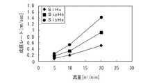
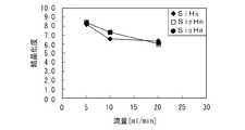
珪素化合物としてSiH4、Si2H6及びSi3H8ガスを、プラズマ生成用ガスとしてArガスを使用し、プラズマCVD装置100において下記のプラズマCVD条件で成膜ガスの流量を変えてポリシリコン膜を成膜した。各条件で成膜されたポリシリコン膜の成膜レートを図4、結晶化度を図5に示した。なお、結晶化度は、ラマン分光分析で得られたスペクトルの結晶性シリコン(520nm)の信号強度をアモルファスシリコン(480nm)の信号強度で除した値である。Next, experimental data on which the present invention is based will be given and suitable conditions for the plasma CVD process will be described.
Experiment 1:
SiH4 , Si2 H6 and Si3 H8 gases are used as silicon compounds, Ar gas is used as a plasma generating gas, and polysilicon is produced by changing the flow rate of the film forming gas under the following plasma CVD conditions in the
[プラズマCVD条件]
処理温度(載置台):400℃
マイクロ波パワー:3000W
処理圧力;5.3Pa
シラン系ガス流量;5、10又は20mL/min(sccm)
Arガス流量;上記シラン系ガスとの合計で800mL/min(sccm)[Plasma CVD conditions]
Processing temperature (mounting table): 400 ° C
Microwave power: 3000W
Processing pressure: 5.3 Pa
Silane gas flow rate: 5, 10 or 20 mL / min (sccm)
Ar gas flow rate: 800 mL / min (sccm) in total with the silane-based gas
図4から、成膜レートは、どの珪素化合物でも流量の増加に比例して高くなる傾向を示しているが、Si3H8を使用した場合が最も高く、次にSi2H6であり、SiH4は最も低い結果となった。SiH4の成膜レートに対して、Si3H8は約3倍、Si2H6は約2倍の顕著な改善を示した。また、図5から、結晶化度は、どの珪素化合物でも、流量の増加とともに若干減少する傾向が見られるが、珪素化合物の種類による違いは少なく、略同等の膜質であることが確認された。From FIG. 4, the film formation rate tends to increase in proportion to the increase in the flow rate for any silicon compound, but the highest when Si3 H8 is used, followed by Si2 H6 . SiH4 gave the lowest results. Si3 H8 showed a remarkable improvement of about 3 times and Si2 H6 of about 2 times the SiH4 deposition rate. Further, FIG. 5 shows that the crystallinity tends to slightly decrease with an increase in the flow rate of any silicon compound, but there is little difference depending on the type of silicon compound, and it has been confirmed that the film quality is substantially equivalent.
また、図6は、珪素化合物としてSiH4およびSi2H6を使用し上記条件で成膜したポリシリコン膜をXRD分析し、結晶方位<220>の信号強度を膜厚で規格化した比率(%)と、SiH4およびSi2H6の流量との関係を示している。なお、図6には、成膜レート(縦軸の右側目盛り)も併記した。図6のXRD分析でもラマン分光分析と同様の傾向を示し、結晶方位<220>の比率は、SiH4およびSi2H6ともに流量の増加とともに若干減少する傾向が見られるが、珪素化合物による違いは少なく、略同等の膜質であることが確認された。しかし、成膜レートは、SiH4に比べてSi2H6は約2倍の顕著な改善を示した。Further, FIG. 6 shows a ratio of the signal strength of the crystal orientation <220> normalized by the film thickness by XRD analysis of a polysilicon film formed under the above conditions using SiH4 and Si2 H6 as silicon compounds ( %) And the flow rates of SiH4 and Si2 H6 . In FIG. 6, the film formation rate (right scale on the vertical axis) is also shown. The XRD analysis of FIG. 6 shows the same tendency as the Raman spectroscopic analysis, and the ratio of the crystal orientation <220> tends to slightly decrease with increasing flow rate for both SiH4 and Si2 H6. It was confirmed that the film quality was almost the same. However, the deposition rate of Si2 H6 was about twice as great as that of SiH4 .
以上の結果から、珪素化合物ガスの体積流量比率(珪素化合物ガス/合計成膜ガス流量の百分率)が1.25%以上2.5%以下の範囲内で、SiH4に比較して、Si2H6及びSi3H8を用いることの優位性が際立っていることが理解される。従って、珪素化合物として、分子中に含まれる珪素原子の数が2以上である珪素化合物を用いることにより、ポリシリコン膜の結晶化度を低下させることなく、成膜レートを大幅に向上できることが確認された。From the above results, the volume flow rate ratio of silicon compound gas (silicon compound gas / percentage of total film forming gas flow rate) is within the range of 1.25% to 2.5%, compared to SiH4 , Si2. It is understood that the advantages of using H6 and Si3 H8 are significant. Therefore, it has been confirmed that by using a silicon compound having two or more silicon atoms in the molecule as the silicon compound, the deposition rate can be significantly improved without reducing the crystallinity of the polysilicon film. It was done.
実験2:
珪素化合物としてSi2H6、プラズマ生成用ガスとしてH2ガスを使用し、プラズマCVD装置100において下記のプラズマCVD条件でポリシリコン膜を成膜した。各条件で成膜されたポリシリコン膜をXRD分析し、結晶方位<220>の信号強度を膜厚で規格化した比率(%)を元に、膜質に対する成膜圧力、温度、及びマイクロ波出力の影響を調べた。結果を図7〜9に示した。Experiment 2:
Using Si2 H6 as the silicon compound and H2 gas as the plasma generating gas, a polysilicon film was formed in the
[プラズマCVD条件]
処理温度(載置台):250℃、400℃又は500℃に設定した。
マイクロ波パワー:2000W、3000W又は4000Wに設定した。
処理圧力;4Pa、5.3Pa又は10.6Paに設定した。
シラン系ガス流量;5mL/min(sccm)に設定した。
H2ガス流量;上記シラン系ガスとの合計で400mL/min(sccm)に設定した。[Plasma CVD conditions]
Treatment temperature (mounting table): set to 250 ° C, 400 ° C or 500 ° C.
Microwave power: set to 2000W, 3000W or 4000W.
Processing pressure: 4 Pa, 5.3 Pa or 10.6 Pa was set.
Silane-based gas flow rate: 5 mL / min (sccm).
H2 gas flow rate: 400 mL / min (sccm) in total with the silane-based gas.
図7は成膜圧力の影響を示しており、圧力が4Paから5.3Paでは結晶方位<220>の比率はほとんど変化していないが、10.6Paでは大幅に低下していた。従って、成膜圧力は、例えば10.6Pa以下が好ましく、5.3Pa以下がより好ましいと考えられる。 FIG. 7 shows the influence of the film forming pressure. When the pressure is 4 Pa to 5.3 Pa, the ratio of the crystal orientation <220> hardly changes, but when the pressure is 10.6 Pa, the ratio is greatly reduced. Accordingly, the film forming pressure is preferably 10.6 Pa or less, for example, and more preferably 5.3 Pa or less.
図8は成膜温度(載置台の温度)の影響を示しており、250℃、400℃、500℃で結晶方位<220>の比率はほとんど変化しておらず、有意な差は認められなかった。ただし、成膜温度が500℃を超えて高くなると結晶方位<220>の比率が低下する傾向が見られるため、成膜温度の上限は600℃程度とすることが好ましいと考えられる。従って、成膜温度は、例えば250℃以上600℃以下が好ましく、250℃から500℃がより好ましい。 FIG. 8 shows the influence of the film formation temperature (mounting table temperature). The ratio of crystal orientation <220> hardly changed at 250 ° C., 400 ° C., and 500 ° C., and no significant difference was observed. It was. However, since the ratio of the crystal orientation <220> tends to decrease when the film forming temperature is higher than 500 ° C., the upper limit of the film forming temperature is preferably set to about 600 ° C. Therefore, the film formation temperature is preferably 250 ° C. or more and 600 ° C. or less, and more preferably 250 ° C. to 500 ° C.
図9はマイクロ波出力の影響を示しており、マイクロ波出力を2000Wから4000Wに大きくすることによって、結晶方位<220>の比率が増加することが確認された。図9から、マイクロ波出力を大きくするほど結晶化度を高めることが可能であることが示唆された。従って、マイクロ波出力は、例えば2000W以上5000W以下が好ましく、3000W以上5000W以下がより好ましいと考えられる。 FIG. 9 shows the influence of the microwave output, and it was confirmed that the ratio of the crystal orientation <220> was increased by increasing the microwave output from 2000 W to 4000 W. FIG. 9 suggests that the crystallinity can be increased as the microwave output is increased. Therefore, it is considered that the microwave output is preferably 2000 W or more and 5000 W or less, and more preferably 3000 W or more and 5000 W or less.
[不揮発性メモリ装置の製造への適用例]
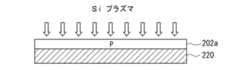
次に、図10〜図15を参照しながら、本実施の形態に係る結晶性珪素膜の製造方法を不揮発性メモリ装置の製造過程に適用した例について説明する。図10は、クロスポイント型のメモリセルアレイ200の構成を模式的に示している。メモリセルアレイ200は複数本(図示では3本)のビット線BLと複数本(図示では3本)のワード線WLの交点にメモリセルMCが配置されている。[Example of application to manufacture of non-volatile memory device]
Next, an example in which the method for manufacturing a crystalline silicon film according to the present embodiment is applied to a manufacturing process of a nonvolatile memory device will be described with reference to FIGS. FIG. 10 schematically shows a configuration of a cross-point type
図11は、図10のメモリセルアレイ200の要部断面図であり、メモリセルMCの詳細な構造を示している。メモリセルMCは、ダイオード201と記憶素子211とが直列に接続した回路構造をしている。ダイオード201は、pinダイオードであり、p型シリコン層202、真性シリコン層203及びn型シリコン層204を備えている。 FIG. 11 is a fragmentary cross-sectional view of the
記憶素子211としては、抵抗変化メモリ(RRAM)の場合は電気的ストレスによって抵抗変化する材料(例えば、PrCaMnO等の遷移金属酸化物)、相変化メモリ(PRAM)の場合は電流による熱ストレスにより相変化する材料(例えばGeSeTe等)、強誘電体メモリ(FeRAM)の場合は強誘電体材料(例えば、チタン酸ジルコン酸鉛、ストロンチウム・ビスマス・タンタル複合酸化物等)、磁気メモリ(MRAM)の場合は、例えばFe、Co、Ni、CoFe、NiFeなどの遷移金属磁性元素・それらの合金などからなる強磁性層と非磁性層と前記強磁性層とが積層されたTMR(強磁性トンネル磁気抵抗効果)素子構造など、を有するものを挙げることができる。 In the case of a resistance change memory (RRAM), the
本発明に係るポリシリコン膜の製造方法は、クロスポイント型のメモリセルアレイ200のダイオード201を製造する際に適用できる。図12及び図13に示すように、図示しない層間絶縁膜上に形成された下部電極層220(ワードラインWLとなるもの)の上に、プラズマCVD装置100により分子中に含まれる珪素原子の数が2以上である珪素化合物を含む成膜ガスを使用してポリシリコン層202a(p型シリコン層202となる部分)を成膜する。この工程では、ドーパントガス供給源19dから、B2H6等のドーパントガスを供給しながらプラズマCVDを行う。The method for manufacturing a polysilicon film according to the present invention can be applied when manufacturing the
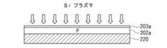
次に、図13及び図14に示すように、ポリシリコン層202aの上に、プラズマCVD装置100により分子中に含まれる珪素原子の数が2以上である珪素化合物を含む成膜ガスを使用してポリシリコン層203a(真性シリコン層203となる部分)を成膜する。 Next, as shown in FIGS. 13 and 14, a film forming gas containing a silicon compound in which the number of silicon atoms contained in the molecule is 2 or more is used on the
次に、図14及び図15に示すように、ポリシリコン層203aの上に、プラズマCVD装置100により分子中に含まれる珪素原子の数が2以上である珪素化合物を含む成膜ガスを使用してポリシリコン層204a(n型シリコン層204となる部分)を成膜する。この工程では、ドーパントガス供給源19dから、PH3等のドーパントガスを供給しながらプラズマCVDを行う。Next, as shown in FIGS. 14 and 15, a film forming gas containing a silicon compound in which the number of silicon atoms contained in the molecule is 2 or more is used on the
以上のようにして、p型シリコン層202となるポリシリコン層202a、真性シリコン層203となるポリシリコン層203a及びn型シリコン層204となるポリシリコン層204aを順次形成することができる。以降は、ポリシリコン層204aの上に、記憶素子211となる部分の材料膜を形成し、エッチングを行うことによって、図11に示した積層構造のメモリセルMCを形成できる。 As described above, the
本発明方法を適用することによって、高い成膜レートで高い結晶化度の良質なポリシリコン層202a,203a及び204aを成膜できる。また、本発明方法では、平面アンテナにより処理容器内にマイクロ波を導入してプラズマを生成する方式のプラズマCVD装置100を用いることによって、600℃以下の低温でポリシリコン層202a,203a及び204aを成膜できるので、成膜の過程でドーパントの拡散を生じさせることがない。また、通常、図10に示すようなメモリセルアレイ200を積層構造とすることによって集積度の向上を図っている。そのためには、p型シリコン層202、真性シリコン層203及びn型シリコン層204からなるダイオード201(pinダイオード)は、出来るだけ薄く形成する必要がある。しかし、熱CVD法によってポリシリコン層202a,203a及び204aを成膜する場合には、薄膜化が困難であるとともに、高温によってドーパントの拡散が生じてしまう。このような観点から、ポリシリコン層202a,203a及び204aを薄膜に成膜できるとともに、比較的低温での成膜が可能でドーパントの拡散を生じさせない本発明方法を適用することは極めて有利である。 By applying the method of the present invention, high-
以上、本発明の実施形態を述べたが、本発明は上記実施形態に制約されることはなく、種々の変形が可能である。例えば、上記実施の形態では、クロスポイント型不揮発性メモリ装置の製造工程での適用例を挙げて説明したが、これに限るものではなく、良質な結晶性珪素薄膜を高いレートで成膜する必要がある半導体プロセスに広く適用できる。 As mentioned above, although embodiment of this invention was described, this invention is not restrict | limited to the said embodiment, A various deformation | transformation is possible. For example, in the above-described embodiment, the application example in the manufacturing process of the cross-point type nonvolatile memory device has been described. However, the present invention is not limited to this, and it is necessary to form a high-quality crystalline silicon thin film at a high rate. It can be widely applied to some semiconductor processes.
1…処理容器、2…載置台、3…支持部材、5…ヒータ、9…高周波電源、12…排気管、14…ガス導入部、14a…第1のガス導入部、14b…第2のガス導入部、16…搬入出口、17…ゲートバルブ、18…ガス供給装置、19a…不活性ガス供給源、19b…水素ガス供給源、19c…珪素化合物ガス(Si化合物ガス)供給源、19d…ドーパントガス供給源、19e…水素ガス供給源、24…排気装置、27…マイクロ波導入装置、28…透過板、29…シール部材、31…平面アンテナ、32…マイクロ波放射孔、37…導波管、39…マイクロ波発生装置、50…制御部、100…プラズマCVD装置、W…シリコンウエハ(基板) DESCRIPTION OF
Claims (11)
Translated fromJapanese被処理体を収容する上部が開口した処理容器と、
前記処理容器内に配置され、被処理体を載置する載置台と、
前記処理容器の前記開口を塞ぐ誘電体部材と、
前記誘電体部材の上部に設けられ、前記処理容器内にマイクロ波を導入するための複数の孔を有する平面アンテナと、
前記処理容器内に成膜ガスを導入するガス導入部と、
前記処理容器内を減圧排気する排気装置と、
前記処理容器内に前記ガス導入部を介して導入した式SinH2n+2(ここで、nは2以上の数を意味する)で表される珪素化合物を含む成膜ガスを、前記平面アンテナを介して導入した前記マイクロ波により励起してプラズマを生成させ、該プラズマを用いてプラズマCVDを行い被処理体の表面に結晶性珪素膜を堆積させる結晶性珪素膜の成膜方法が行われるように制御する制御部と、
を備えたことを特徴とするプラズマCVD装置。A plasma CVD apparatus for forming a crystalline silicon film on an object to be processed by a plasma CVD method,
A processing container having an open top for accommodating the object to be processed;
A mounting table disposed in the processing container and on which a target object is mounted;
A dielectric member that closes the opening of the processing container;
A planar antenna provided on top of the dielectric member and having a plurality of holes for introducing microwaves into the processing vessel;
A gas introduction part for introducing a film forming gas into the processing container;
An exhaust device for evacuating the inside of the processing vessel;
A film-forming gas containing a silicon compound represented by the formula Sin H2n + 2 (where n means a number of 2 or more) introduced into the processing vessel through the gas introduction unit is used for the planar antenna. A method of forming a crystalline silicon film is performed in which plasma is generated by excitation with the microwave introduced through the plasma, and plasma CVD is performed using the plasma to deposit a crystalline silicon film on the surface of the object to be processed. A control unit for controlling
A plasma CVD apparatus comprising:
前記電極に接続する高周波電源と、
をさらに備え、
前記制御部は、前記プラズマCVDの間、前記電極に高周波電力を印加することにより、被処理体にバイアス電圧を印加する請求項10に記載のプラズマCVD装置。An electrode embedded in the mounting table,
A high frequency power source connected to the electrode;
Further comprising
The plasma CVD apparatus according to claim 10, wherein the control unit applies a bias voltage to the object to be processed by applying high-frequency power to the electrode during the plasma CVD.
Priority Applications (6)
| Application Number | Priority Date | Filing Date | Title |
|---|---|---|---|
| JP2009227639AJP2011077322A (en) | 2009-09-30 | 2009-09-30 | Method for depositing crystalline silicon film and plasma cvd device |
| CN2010800438745ACN102549717A (en) | 2009-09-30 | 2010-09-28 | Method for forming crystalline silicon film and plasma CVD device |
| KR1020127008193AKR20120059593A (en) | 2009-09-30 | 2010-09-28 | Method for forming crystalline silicon film and plasma cvd device |
| PCT/JP2010/066794WO2011040394A1 (en) | 2009-09-30 | 2010-09-28 | Method for forming crystalline silicon film and plasma cvd device |
| US13/499,150US20120315745A1 (en) | 2009-09-30 | 2010-09-28 | Crystalline silicon film forming method and plasma cvd apparatus |
| TW099132912ATW201131006A (en) | 2009-09-30 | 2010-09-29 | Method for depositing crystalline silicon film and plasma cvd device |
Applications Claiming Priority (1)
| Application Number | Priority Date | Filing Date | Title |
|---|---|---|---|
| JP2009227639AJP2011077322A (en) | 2009-09-30 | 2009-09-30 | Method for depositing crystalline silicon film and plasma cvd device |
Publications (1)
| Publication Number | Publication Date |
|---|---|
| JP2011077322Atrue JP2011077322A (en) | 2011-04-14 |
Family
ID=43826209
Family Applications (1)
| Application Number | Title | Priority Date | Filing Date |
|---|---|---|---|
| JP2009227639APendingJP2011077322A (en) | 2009-09-30 | 2009-09-30 | Method for depositing crystalline silicon film and plasma cvd device |
Country Status (6)
| Country | Link |
|---|---|
| US (1) | US20120315745A1 (en) |
| JP (1) | JP2011077322A (en) |
| KR (1) | KR20120059593A (en) |
| CN (1) | CN102549717A (en) |
| TW (1) | TW201131006A (en) |
| WO (1) | WO2011040394A1 (en) |
Cited By (3)
| Publication number | Priority date | Publication date | Assignee | Title |
|---|---|---|---|---|
| WO2013161819A1 (en)* | 2012-04-24 | 2013-10-31 | 東京エレクトロン株式会社 | Plasma processing method and plasma processing apparatus |
| WO2014002586A1 (en)* | 2012-06-27 | 2014-01-03 | 東京エレクトロン株式会社 | Plasma processing method and plasma processing apparatus |
| CN103526178A (en)* | 2012-07-04 | 2014-01-22 | 东京毅力科创株式会社 | Silicon oxide film forming method and forming apparatus |
Families Citing this family (7)
| Publication number | Priority date | Publication date | Assignee | Title |
|---|---|---|---|---|
| CN103602957A (en)* | 2013-11-07 | 2014-02-26 | 中山市创科科研技术服务有限公司 | Equipment for preparing alpha_SiH membrane |
| KR20150087702A (en)* | 2014-01-22 | 2015-07-30 | 삼성전자주식회사 | Plasma generating apparatus |
| JP6742165B2 (en)* | 2016-06-14 | 2020-08-19 | 東京エレクトロン株式会社 | Method for treating silicon nitride film and method for forming silicon nitride film |
| JP7022651B2 (en)* | 2018-05-28 | 2022-02-18 | 東京エレクトロン株式会社 | Film etching method and plasma processing equipment |
| US12159768B2 (en)* | 2019-03-25 | 2024-12-03 | Recarbon, Inc. | Controlling exhaust gas pressure of a plasma reactor for plasma stability |
| US10832893B2 (en)* | 2019-03-25 | 2020-11-10 | Recarbon, Inc. | Plasma reactor for processing gas |
| CN114196946B (en)* | 2021-12-10 | 2024-12-06 | 成都稳正科技有限公司 | A multi-mode non-cylindrical resonant cavity MPCVD device with a conical reflective top surface |
Citations (4)
| Publication number | Priority date | Publication date | Assignee | Title |
|---|---|---|---|---|
| JPH0817738A (en)* | 1994-06-24 | 1996-01-19 | Mitsui Toatsu Chem Inc | Method for forming crystalline semiconductor thin film |
| JP2006216955A (en)* | 2005-02-04 | 2006-08-17 | Asm America Inc | Method for depositing electrically active doped crystalline Si-containing films |
| JP2008127274A (en)* | 2006-11-17 | 2008-06-05 | Sharp Corp | Formation of single crystal silicon on glass by film transfer. |
| JP2008277306A (en)* | 1997-01-29 | 2008-11-13 | Foundation For Advancement Of International Science | Plasma device |
Family Cites Families (2)
| Publication number | Priority date | Publication date | Assignee | Title |
|---|---|---|---|---|
| KR950001360B1 (en)* | 1990-11-26 | 1995-02-17 | 가부시키가이샤 한도오따이 에네루기 겐큐쇼 | Electro-optical device and its driving method |
| US6337229B1 (en)* | 1994-12-16 | 2002-01-08 | Semiconductor Energy Laboratory Co., Ltd. | Method of making crystal silicon semiconductor and thin film transistor |
- 2009
- 2009-09-30JPJP2009227639Apatent/JP2011077322A/enactivePending
- 2010
- 2010-09-28KRKR1020127008193Apatent/KR20120059593A/ennot_activeCeased
- 2010-09-28WOPCT/JP2010/066794patent/WO2011040394A1/enactiveApplication Filing
- 2010-09-28CNCN2010800438745Apatent/CN102549717A/enactivePending
- 2010-09-28USUS13/499,150patent/US20120315745A1/ennot_activeAbandoned
- 2010-09-29TWTW099132912Apatent/TW201131006A/enunknown
Patent Citations (4)
| Publication number | Priority date | Publication date | Assignee | Title |
|---|---|---|---|---|
| JPH0817738A (en)* | 1994-06-24 | 1996-01-19 | Mitsui Toatsu Chem Inc | Method for forming crystalline semiconductor thin film |
| JP2008277306A (en)* | 1997-01-29 | 2008-11-13 | Foundation For Advancement Of International Science | Plasma device |
| JP2006216955A (en)* | 2005-02-04 | 2006-08-17 | Asm America Inc | Method for depositing electrically active doped crystalline Si-containing films |
| JP2008127274A (en)* | 2006-11-17 | 2008-06-05 | Sharp Corp | Formation of single crystal silicon on glass by film transfer. |
Cited By (5)
| Publication number | Priority date | Publication date | Assignee | Title |
|---|---|---|---|---|
| WO2013161819A1 (en)* | 2012-04-24 | 2013-10-31 | 東京エレクトロン株式会社 | Plasma processing method and plasma processing apparatus |
| WO2014002586A1 (en)* | 2012-06-27 | 2014-01-03 | 東京エレクトロン株式会社 | Plasma processing method and plasma processing apparatus |
| JP2014011178A (en)* | 2012-06-27 | 2014-01-20 | Tokyo Electron Ltd | Plasma processing method and plasma processing apparatus |
| US9779936B2 (en) | 2012-06-27 | 2017-10-03 | Tokyo Electron Limited | Plasma processing method and plasma processing apparatus |
| CN103526178A (en)* | 2012-07-04 | 2014-01-22 | 东京毅力科创株式会社 | Silicon oxide film forming method and forming apparatus |
Also Published As
| Publication number | Publication date |
|---|---|
| WO2011040394A1 (en) | 2011-04-07 |
| CN102549717A (en) | 2012-07-04 |
| KR20120059593A (en) | 2012-06-08 |
| TW201131006A (en) | 2011-09-16 |
| US20120315745A1 (en) | 2012-12-13 |
Similar Documents
| Publication | Publication Date | Title |
|---|---|---|
| WO2011040394A1 (en) | Method for forming crystalline silicon film and plasma cvd device | |
| JP6002087B2 (en) | Graphene generation method | |
| US8728917B2 (en) | Carbon nanotube forming method and pre-treatment method therefor | |
| US9613859B2 (en) | Direct deposition of nickel silicide nanowire | |
| US8034179B2 (en) | Method for insulating film formation, storage medium from which information is readable with computer, and processing system | |
| WO2011114961A1 (en) | Silicon oxide film forming method, and plasma oxidation apparatus | |
| US9650252B2 (en) | Pretreatment method and carbon nanotube formation method | |
| JP5460011B2 (en) | Silicon nitride film forming method, computer-readable storage medium, and plasma CVD apparatus | |
| US20110086517A1 (en) | Process for producing silicon nitride film, process for producing silicon nitride film laminate, computer-readable storage medium, and plasma cvd device | |
| WO2011040396A1 (en) | Method for forming silicon nitride film, and method for producing semiconductor memory device | |
| JP2014075493A (en) | Deposition method and deposition device | |
| JP5357487B2 (en) | Silicon oxide film forming method, computer-readable storage medium, and plasma oxidation processing apparatus | |
| KR101095318B1 (en) | Modification method and reforming apparatus of titanium nitride film | |
| WO2013172203A1 (en) | Solar cell manufacturing method and plasma processing apparatus | |
| JP5788627B2 (en) | Carbon nanotube growth method | |
| JP2009267391A (en) | Process for producing silicon nitride film, process for producing silicon nitride film laminate, computer-readable storage medium, and plasma cvd device | |
| WO2010113928A1 (en) | Method for forming silicon nitride film, method for manufacturing semiconductor memory device, and plasma cvd apparatus | |
| JP2009246210A (en) | Method for forming silicon nitride film, method for manufacturing silicon nitride film laminate, computer-readable storage medium and plasma cvd apparatus | |
| WO2009123325A1 (en) | Process for producing silicon nitride film, process for producing silicon nitride film laminate, computer-readable storage medium, and plasma cvd device |
Legal Events
| Date | Code | Title | Description |
|---|---|---|---|
| A621 | Written request for application examination | Free format text:JAPANESE INTERMEDIATE CODE: A621 Effective date:20120927 | |
| A131 | Notification of reasons for refusal | Free format text:JAPANESE INTERMEDIATE CODE: A131 Effective date:20130827 | |
| A521 | Request for written amendment filed | Free format text:JAPANESE INTERMEDIATE CODE: A523 Effective date:20130928 | |
| A02 | Decision of refusal | Free format text:JAPANESE INTERMEDIATE CODE: A02 Effective date:20140513 |