JP2011061343A - Drive device and display device - Google Patents
Drive device and display deviceDownload PDFInfo
- Publication number
- JP2011061343A JP2011061343AJP2009206658AJP2009206658AJP2011061343AJP 2011061343 AJP2011061343 AJP 2011061343AJP 2009206658 AJP2009206658 AJP 2009206658AJP 2009206658 AJP2009206658 AJP 2009206658AJP 2011061343 AJP2011061343 AJP 2011061343A
- Authority
- JP
- Japan
- Prior art keywords
- voltage
- power supply
- output amplifier
- bias
- bias voltage
- Prior art date
- Legal status (The legal status is an assumption and is not a legal conclusion. Google has not performed a legal analysis and makes no representation as to the accuracy of the status listed.)
- Pending
Links
Images


Classifications
- H—ELECTRICITY
- H03—ELECTRONIC CIRCUITRY
- H03F—AMPLIFIERS
- H03F3/00—Amplifiers with only discharge tubes or only semiconductor devices as amplifying elements
- H03F3/45—Differential amplifiers
- H03F3/45071—Differential amplifiers with semiconductor devices only
- H03F3/45076—Differential amplifiers with semiconductor devices only characterised by the way of implementation of the active amplifying circuit in the differential amplifier
- H03F3/45179—Differential amplifiers with semiconductor devices only characterised by the way of implementation of the active amplifying circuit in the differential amplifier using MOSFET transistors as the active amplifying circuit
- H03F3/45183—Long tailed pairs
- H—ELECTRICITY
- H03—ELECTRONIC CIRCUITRY
- H03F—AMPLIFIERS
- H03F3/00—Amplifiers with only discharge tubes or only semiconductor devices as amplifying elements
- H03F3/45—Differential amplifiers
- H03F3/45071—Differential amplifiers with semiconductor devices only
- H03F3/45076—Differential amplifiers with semiconductor devices only characterised by the way of implementation of the active amplifying circuit in the differential amplifier
- H03F3/45475—Differential amplifiers with semiconductor devices only characterised by the way of implementation of the active amplifying circuit in the differential amplifier using IC blocks as the active amplifying circuit
- H—ELECTRICITY
- H03—ELECTRONIC CIRCUITRY
- H03F—AMPLIFIERS
- H03F2200/00—Indexing scheme relating to amplifiers
- H03F2200/375—Circuitry to compensate the offset being present in an amplifier
- H—ELECTRICITY
- H03—ELECTRONIC CIRCUITRY
- H03F—AMPLIFIERS
- H03F2200/00—Indexing scheme relating to amplifiers
- H03F2200/405—Indexing scheme relating to amplifiers the output amplifying stage of an amplifier comprising more than three power stages
- H—ELECTRICITY
- H03—ELECTRONIC CIRCUITRY
- H03F—AMPLIFIERS
- H03F2200/00—Indexing scheme relating to amplifiers
- H03F2200/411—Indexing scheme relating to amplifiers the output amplifying stage of an amplifier comprising two power stages
- H—ELECTRICITY
- H03—ELECTRONIC CIRCUITRY
- H03F—AMPLIFIERS
- H03F2203/00—Indexing scheme relating to amplifiers with only discharge tubes or only semiconductor devices as amplifying elements covered by H03F3/00
- H03F2203/45—Indexing scheme relating to differential amplifiers
- H03F2203/45101—Control of the DC level being present
- H—ELECTRICITY
- H03—ELECTRONIC CIRCUITRY
- H03F—AMPLIFIERS
- H03F2203/00—Indexing scheme relating to amplifiers with only discharge tubes or only semiconductor devices as amplifying elements covered by H03F3/00
- H03F2203/45—Indexing scheme relating to differential amplifiers
- H03F2203/45512—Indexing scheme relating to differential amplifiers the FBC comprising one or more capacitors, not being switched capacitors, and being coupled between the LC and the IC
- H—ELECTRICITY
- H03—ELECTRONIC CIRCUITRY
- H03F—AMPLIFIERS
- H03F2203/00—Indexing scheme relating to amplifiers with only discharge tubes or only semiconductor devices as amplifying elements covered by H03F3/00
- H03F2203/45—Indexing scheme relating to differential amplifiers
- H03F2203/45674—Indexing scheme relating to differential amplifiers the LC comprising one current mirror
Landscapes
- Engineering & Computer Science (AREA)
- Power Engineering (AREA)
- Liquid Crystal Display Device Control (AREA)
- Control Of Indicators Other Than Cathode Ray Tubes (AREA)
- Electronic Switches (AREA)
- Amplifiers (AREA)
Abstract
Translated fromJapaneseDescription
Translated fromJapanese本発明は、複数の出力アンプ回路を備える駆動装置、及び駆動装置を搭載した表示装置に関する。 The present invention relates to a drive device including a plurality of output amplifier circuits, and a display device equipped with the drive device.
半導体集積回路装置に配設された回路に発生する電源電圧降下の影響をなくし、回路の動作不具合や動作速度低下を抑制する方法が特許文献1に提案されている。図7に、特許文献1に開示された半導体集積回路装置の回路構成図を示す。半導体集積回路装置200には、電源端子112、グランド端子(グランドパッド)114、及び負電源端子116が設けられている。電源端子112には、外部の電源が接続され電源電圧(Vdd)が供給される。グランド端子114は、グランド(0V)に接続される。負電源端子116には、外部の負電源が接続され負電源電圧(−Vdd)が供給される。このように、電源及びグランド間の電圧と同じ大きさの電圧が、グランドとの間に発生するように負電源が設けられている。 Patent Document 1 proposes a method of eliminating the influence of a power supply voltage drop generated in a circuit provided in a semiconductor integrated circuit device and suppressing a malfunction of the circuit and a decrease in operation speed. FIG. 7 shows a circuit configuration diagram of the semiconductor integrated circuit device disclosed in Patent Document 1. In FIG. The semiconductor integrated
また、電源端子112には電源配線118が接続され、グランド端子114にはグランド配線120が接続されている。電源配線118とグランド配線120との間には、電源及びグランドに近い順に第1回路301から第f回路30fまでの複数の回路が並列接続されている。 In addition, a
さらに、複数の回路のうち、グランドから最も離れた領域に配置された第f回路30fの、グランド配線120側のノードGfと負電源端子116との間には電流発生部として電流源122が配置されている。すなわち、電流源122は、グランド配線120にグランド電位(0V)を供給するグランド端子(グランドパッド)114から最も離れた配線部分に設けられており、グランド配線120に流れる電流の方向がグランドから負電源(電流源122)方向となるように電流を発生する。 Further, among the plurality of circuits, a
負電源に接続された電流源122を配置することにより、グランド配線120を流れる電流の方向はグランドからノードGfへの方向となり、グランド配線120上のノードの電位は、グランドから離れるに従って(G1、G2・・・Gfの順に)低くなり、ノードGfで最も低くなる。また、電源配線118上のノードの電位は、電源から離れるに従って(V1、V2・・・Vfの順に)低くなるため、各回路301〜30fにおける電源側ノードとグランド側ノード間で十分な電位差を確保でき、電源(グランド)から離れた位置に配置された回路であっても電圧レベルが低下せず、電源電圧降下及びグランド電圧上昇の影響を受けない、安定した回路となる。 By arranging the
近年、テレビやパソコン用ディスプレイに使用される液晶表示装置は、大画面化、高精細化、多機能化等が進んでいる。これに伴って、液晶表示パネルを駆動するソースドライバ(駆動装置)の出力数が増大し、その構成が複雑化してきている。 In recent years, liquid crystal display devices used for television and personal computer displays have been increasing in screen size, definition, and multifunction. Along with this, the number of outputs of the source driver (driving device) for driving the liquid crystal display panel has increased, and its configuration has become complicated.
ソースドライバに配設された電源配線、及びグランド配線の引き回しによって高抵抗化が生じると、電源電圧供給源から離れた位置に配置される回路において、供給電圧の電圧降下が発生する。また、消費電力の節約や、回路の高速化を目的とした低電源電圧化を実施すると、電源電圧供給源から離れた位置に配置される回路において、供給電圧の電圧降下が発生する。供給電圧の電圧降下は、回路の動作不具合、動作速度低下、各出力アンプ回路間のスルーレート(駆動能力)のばらつきなどの原因となり、表示画質不良等が発生する。 When the resistance increases due to the routing of the power supply wiring and the ground wiring arranged in the source driver, a voltage drop of the supply voltage occurs in a circuit arranged at a position away from the power supply voltage supply source. Further, when the power supply voltage is reduced for the purpose of saving power consumption or increasing the speed of the circuit, a voltage drop of the supply voltage occurs in a circuit arranged at a position away from the power supply voltage supply source. The voltage drop of the supply voltage causes a malfunction of the circuit, a decrease in the operation speed, a variation in slew rate (drive capability) between the output amplifier circuits, and a display image quality defect occurs.
多出力化に対応した最近のソースドライバにおいては、液晶表示パネルの長尺方向に出力アンプ回路を1000個近く並べたレイアウトのものもある。このような構成においては、電源電圧供給源から離れた位置に配置される出力アンプ回路の供給電圧の電圧降下が特に深刻となる。 Some recent source drivers that support multi-output have a layout in which nearly 1000 output amplifier circuits are arranged in the longitudinal direction of the liquid crystal display panel. In such a configuration, the voltage drop of the supply voltage of the output amplifier circuit arranged at a position away from the power supply voltage supply source becomes particularly serious.
上記特許文献1の技術を適用した場合、上述したように、内部回路の電源電圧とGNDとの電圧差を補正することが可能となる。しかしながら、上記特許文献1の技術においても、電源電圧供給源から離れた位置に配置される出力アンプ回路と、電源電圧供給源に近い位置に配置される出力アンプ回路とで駆動能力のばらつきが生じるという問題を解決することはできなかった。 When the technique of Patent Document 1 is applied, as described above, the voltage difference between the power supply voltage of the internal circuit and GND can be corrected. However, also in the technique of the above-mentioned Patent Document 1, the driving capability varies between the output amplifier circuit arranged at a position away from the power supply voltage supply source and the output amplifier circuit arranged at a position close to the power supply voltage supply source. It was not possible to solve the problem.
本発明に係る駆動装置は、並列接続された複数の出力アンプ回路と、前記複数の出力アンプ回路に、バイアス電圧供給源からバイアス電圧を供給するバイアス配線と、前記複数の出力アンプ回路に、電源電圧供給源から電源電圧を供給する電源配線と、前記複数の出力アンプ回路に供給される前記電源電圧と前記バイアス電圧との差が所望となるように、前記バイアス電圧にオフセット電圧を重畳する補正手段とを備えたものである。 The drive device according to the present invention includes a plurality of output amplifier circuits connected in parallel, a bias wiring for supplying a bias voltage from a bias voltage supply source to the plurality of output amplifier circuits, and a power source for the plurality of output amplifier circuits. Correction for superimposing the offset voltage on the bias voltage so that a difference between the power supply wiring for supplying the power supply voltage from the voltage supply source and the power supply voltage supplied to the plurality of output amplifier circuits and the bias voltage is desired. Means.
本発明に係る駆動装置によれば、複数の出力アンプ回路に供給される電源電圧とバイアス電圧との電圧差が所望となるように、バイアス電圧を補正する補正手段を設けたので、並列接続された複数の出力アンプ回路において所望の駆動能力を実現することができる。 According to the driving device of the present invention, the correction means for correcting the bias voltage is provided so that the voltage difference between the power supply voltage and the bias voltage supplied to the plurality of output amplifier circuits is desired. In addition, a desired driving capability can be realized in a plurality of output amplifier circuits.
本発明に係る表示装置は、上記駆動装置を搭載したものである。 A display device according to the present invention is equipped with the drive device.
本発明によれば、並列接続された複数の出力アンプ回路において所望の駆動能力を実現することができる駆動装置、及び表示装置を提供することができるという優れた効果を有する。 According to the present invention, it is possible to provide a driving device and a display device that can realize a desired driving capability in a plurality of output amplifier circuits connected in parallel.
以下、本発明を適用した実施形態の一例について説明する。なお、本発明の趣旨に合致する限り、他の実施形態も本発明の範疇に属し得ることは言うまでもない。また、以降の図における各部材のサイズや比率は、説明の便宜上のものであり、実際のものとは異なる。 Hereinafter, an example of an embodiment to which the present invention is applied will be described. It goes without saying that other embodiments may also belong to the category of the present invention as long as they match the gist of the present invention. Moreover, the size and ratio of each member in the following drawings are for convenience of explanation, and are different from actual ones.
[実施形態1]
表示装置として、アクティブマトリクス駆動方式の液晶表示装置を例にとり説明する。図1は、アクティブマトリクス駆動方式の液晶表示装置の模式的説明図である。同図において、表示領域50の1画素に接続される主要な構成を等価回路図も模式的に図示する。[Embodiment 1]
As an example of the display device, an active matrix liquid crystal display device will be described. FIG. 1 is a schematic explanatory diagram of an active matrix liquid crystal display device. In the figure, an equivalent circuit diagram is also schematically shown for the main configuration connected to one pixel in the
アクティブマトリクス駆動方式の液晶表示装置100は、アレイ基板と対向基板間に液晶層が挟持された構造となっている。アレイ基板は、通常、表示領域50に透明な画素電極51及び薄膜トランジスタ(以降、「TFT(Thin Film Transistor)」と称する)52がマトリックス上に配置されている。対向基板には、面全体に1つの透明な共通電極53が形成されている。液晶は、容量性を有し、画素電極51と共通電極53との間に液晶容量54を成す。液晶の容量性を補助するために、補助容量55をさらに備えることが多い。なお、共通電極53は、アレイ基板上に配設されていてもよい。 The active matrix drive type liquid
TFT52のオン、オフは、走査信号により制御される。TFT52がオンのとき、映像データ信号に対応した諧調信号電圧が画素電極51に印加され、各画素電極51と、共通電極53との間の電位差により液晶の透過率が変化する。液晶容量54及び補助容量55により、TFT52のオフ後も前述の電位差を一定期間保持することにより、画像が表示される。 On / off of the
アレイ基板上には、各画素電極51に印加する複数のレベル電圧(諧調信号電圧)を送るソース線2(21、22、・・・2n)と、走査信号を送るゲート線4(41、42、・・・4m)とが格子状に配設されている。図1の例においては、ソース線2は、Y方向に延在され、X方向に複数配設されている。一方、ゲート線4は、X方向に延在され、Y方向に複数配設されている。ゲート線4及びソース線2は、互いの交差部に生じる容量や共通電極との間に挟まれる液晶容量54等により、大きな容量性負荷となっている。On the array substrate, a source line 2 (21 , 22 ,... 2n ) for sending a plurality of level voltages (tone signal voltages) applied to each
ソース線2は、表示領域50の外側に区画される額縁領域に配設された駆動装置(ドライバLSI(Large Scale Integration))であるソースドライバ1まで延設されている。同様にして、ゲート線4は、額縁領域に配設された駆動装置であるゲートドライバ3まで延設されている。ソースドライバ1及びゲートドライバ3には、表示コントローラー(不図示)よりそれぞれ必要なクロックCLK、制御信号、電源電圧等が供給される。また、ソースドライバ1には、表示コントローラーより映像データが供給される。 The source line 2 extends to the source driver 1 which is a driving device (driver LSI (Large Scale Integration)) disposed in a frame region partitioned outside the
1画素分のデータの書き換えは、1フレーム期間(1/60秒)に行われる。各ゲート線において、1画素毎(ライン毎)に順次選択され、選択期間内に各ソース線より諧調信号電圧が供給される。ゲートドライバ3は、少なくとも2値の走査信号を供給すればよい。これに対して、ソースドライバ1は、ソース線2を諧調数に応じたレベルの諧調信号電圧で駆動する必要がある。このため、ソースドライバ1は、映像データを諧調信号電圧に変換するデコーダと、その諧調信号電圧をソース線2に増幅出力する出力アンプ回路を備えている。デコーダ及び出力アンプ回路は、複数のソース線2に対応して設けられている。 Rewriting of data for one pixel is performed in one frame period (1/60 seconds). Each gate line is sequentially selected for each pixel (each line), and a gradation signal voltage is supplied from each source line within the selection period. The
図2に、ソースドライバ1に配設された出力アンプ回路10の回路図の一例を示す。前述したように、出力アンプ回路10は、ソース線2それぞれに対応して配設されているが、図2においては、1つの出力アンプ回路10を図示する。 FIG. 2 shows an example of a circuit diagram of the
出力アンプ回路10は、電流源トランジスタT1、差動段として機能する入力差動段11、カレントミラー回路12、出力部13を備える。また、出力アンプ回路10には、電源配線31を介して電源電圧が、バイアス供給線21を介してバイアス電圧が供給されるように構成されている。また、Vss配線32を介して接地電圧(Vss)が供給されるように構成されている。 The
実施形態1に係る電流源トランジスタT1として、P型のMOSトランジスタを配置した。無論、N型としてもよい。電流源トランジスタT1のゲートには、バイアス供給線21を介してバイアス電圧が供給されるように構成されている。電流源トランジスタT1のソースには、電源配線31を介して電源電圧が供給されるように構成されている。電流源トランジスタT1のドレインは、入力差動段11と接続されている。 A P-type MOS transistor is disposed as the current source transistor T1 according to the first embodiment. Of course, it may be an N type. A bias voltage is supplied to the gate of the current source transistor T1 via the
入力差動段11には、ペアトランジスタとして機能する第1導電型の第1の差動トランジスタ、及び第2の差動トランジスタが配置されている。本実施形態1においては、第1の差動トランジスタとしてP型のMOSトランジスタ(以降、「第1の差動トランジスタP1」と云う)、第2の差動トランジスタとしてP型のMOSトランジスタ(以降、「第2の差動トランジスタP2」と云う)を配置した。ペアトランジスタは、P型に限定されるものではなくN型としてもよい。 In the input differential stage 11, a first differential transistor of the first conductivity type that functions as a pair transistor and a second differential transistor are disposed. In the first embodiment, the first differential transistor is a P-type MOS transistor (hereinafter referred to as “first differential transistor P1”), and the second differential transistor is a P-type MOS transistor (hereinafter referred to as “first differential transistor P1”). (Referred to as “second differential transistor P2”). The pair transistor is not limited to the P-type, and may be an N-type.
カレントミラー回路12は、入力差動段11と接続される中間段であり、能動負荷部として機能する。カレントミラー回路12には、第2導電型の第1の中間トランジスタ、及び第2の中間トランジスタが配置されている。本実施形態1においては、第1の中間トランジスタとしてN型のMOSトランジスタ(以降、「第1の中間トランジスタN1」と云う)、第2の中間トランジスタとしてN型のMOSトランジスタ(以降、「第2の中間トランジスタN2」と云う)を配置した。カレントミラー構成の第1の中間トランジスタN1、第2の中間トランジスタN2は、差動対の能動負荷として機能し、入力される作動信号をシングルエンド信号に変換する。 The current mirror circuit 12 is an intermediate stage connected to the input differential stage 11 and functions as an active load unit. In the current mirror circuit 12, a first conductivity type first intermediate transistor and a second intermediate transistor are arranged. In the first embodiment, an N-type MOS transistor (hereinafter referred to as “first intermediate transistor N1”) is used as the first intermediate transistor, and an N-type MOS transistor (hereinafter referred to as “second intermediate transistor” is used as the second intermediate transistor). Middle transistor N2 "). The first intermediate transistor N1 and the second intermediate transistor N2 configured as a current mirror function as an active load of a differential pair, and convert an input operation signal into a single-ended signal.
出力部13は、入力差動段11とカレントミラー回路12の間の接続点に接続されており、出力段14と、位相補償容量C1を備える。位相補償容量C1は、出力段14の前後に接続されている。 The output unit 13 is connected to a connection point between the input differential stage 11 and the current mirror circuit 12, and includes an output stage 14 and a phase compensation capacitor C1. The phase compensation capacitor C <b> 1 is connected before and after the output stage 14.
第1の差動トランジスタP1、第2の差動トランジスタP2は、ソースが共通接続されている。そして、この共通接続されたソースは、電流源トランジスタT1のドレインに接続されている。第1の差動トランジスタP1のドレインは、第1の中間トランジスタN1のドレインに接続されている。同様にして、第2の差動トランジスタP2のドレインは、第2の中間トランジスタN2のドレインに接続されている。 The sources of the first differential transistor P1 and the second differential transistor P2 are commonly connected. The commonly connected source is connected to the drain of the current source transistor T1. The drain of the first differential transistor P1 is connected to the drain of the first intermediate transistor N1. Similarly, the drain of the second differential transistor P2 is connected to the drain of the second intermediate transistor N2.
第1の差動トランジスタP1のゲート電極(制御端子)は、反転入力端子(−)に接続されている。また、第2の差動トランジスタP2のゲート電極(制御端子)は、非反転入力端子(+)に接続されている。 The gate electrode (control terminal) of the first differential transistor P1 is connected to the inverting input terminal (−). The gate electrode (control terminal) of the second differential transistor P2 is connected to the non-inverting input terminal (+).
第1の中間トランジスタN1、及び第2の中間トランジスタN2のソースはそれぞれ接地電位VSSに接続されている。また、第1の中間トランジスタN1、及び第2の中間トランジスタN2のゲートは、ノードaにより共通接続されている。ノードaは、第1の差動トランジスタP1のドレインと第1の中間トランジスタN1のドレイン間にあるノードbと接続されている。 The sources of the first intermediate transistor N1 and the second intermediate transistor N2 are respectively connected to the ground potential VSS. The gates of the first intermediate transistor N1 and the second intermediate transistor N2 are commonly connected by a node a. The node a is connected to a node b located between the drain of the first differential transistor P1 and the drain of the first intermediate transistor N1.
第2の差動ランジスタP2のドレインと、第2の中間トランジスタN2のドレイン間にあるノードcは、出力部13の出力段14に接続されている。出力アンプ回路10からの出力は、出力段14からソース線2に送出される。 A node c between the drain of the second differential transistor P2 and the drain of the second intermediate transistor N2 is connected to the output stage 14 of the output unit 13. The output from the
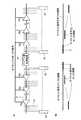
ここで、比較例に係るソースドライバについて説明する。図2に示した出力アンプ回路10に供給するバイアス電圧の供給経路の比較例を図8に示す。バイアス電圧は、ソースドライバ内に配設されたバイアス電圧供給源225から、幹バイアス配線222及びバイアス供給線221を介して、各出力アンプ回路10の電流源トランジスタT(不図示)のゲートに供給される。 Here, a source driver according to a comparative example will be described. FIG. 8 shows a comparative example of the supply path of the bias voltage supplied to the
バイアス電圧供給源225及び電源電圧供給源235は、図8に示すように、ソースドライバのほぼ中央領域に配設されている。幹バイアス配線222は、概ね中央に配設されたバイアス電圧供給源225からソースドライバの左右端部に向けて、図8中のX方向両側に延在されている。そして、幹バイアス配線222から、ソース線202に対応するバイアス供給線221が分岐されている。バイアス供給線221は、出力アンプ回路10の数に対応して配設されている。 As shown in FIG. 8, the bias
次に、ソースドライバの出力アンプ回路の駆動能力について説明する。並列接続された複数の出力アンプ回路に供給される電源電圧とバイアス電圧との電圧差は、図9(a)に示すように、電源電圧供給源やバイアス電圧供給源からの離間距離に関わらず、常に一定であることが望ましい。しかしながら、出力アンプ回路10を駆動することによって大きく電流を消費するため、電流と電源の配線抵抗等との関係から、一時的に電源電圧の落ち込み(いわゆるIRドロップ)が発生する。これに対し、電流を消費しないバイアス電圧は、ほぼ一定の電位を示す。従って、現実的には、図9(a)のような電源電圧とバイアス電圧との電圧差の関係とはならず、図9(b)に示すような電源電圧とバイアス電圧との電圧差の関係となる。図2のような出力アンプ回路10の電流源トランジスタT1において、ソース−ゲート間電圧差(Vgs)が落ち込むと、出力アンプ回路の駆動能力が著しく悪化する。この傾向は、消費電流が積算される電源電圧供給箇所から離れた出力アンプ回路ほど顕著となる。その結果、駆動能力が落ち込んだ出力アンプ回路の出力により、図10のような出力遅延分布となる。そして、ソースドライバ内において、電源電圧供給源から離間した位置において、書き込み不良などの表示画質不良が発生する。 Next, the drive capability of the output amplifier circuit of the source driver will be described. The voltage difference between the power supply voltage and the bias voltage supplied to the plurality of output amplifier circuits connected in parallel is independent of the distance from the power supply voltage supply source and the bias voltage supply source, as shown in FIG. It is desirable that it is always constant. However, since a large amount of current is consumed by driving the
上記特許文献1においては、上述したように。内部回路301〜30fの電源電圧とGNDとの電圧差を補正することができる(図11参照)。しかしながら、図11に示すように、バイアス電圧と電源電圧との電圧差を補正することはできなかった。また、上記特許文献1においては、GND以下の別電源が必要であり、回路内に逆向きの電流源を配置する必要があった。 In Patent Document 1, as described above. The voltage difference between the power supply voltage of the
次に、本実施形態1の特徴部について説明する。図3(a)に、出力アンプ回路10に供給するバイアス電圧の供給経路の一例を示す。バイアス電圧は、ソースドライバ1内に配設されたバイアス電圧供給源25から、バイアス配線として機能する幹バイアス配線22、同じくバイアス配線として機能するバイアス供給線21を介して、各出力アンプ回路10の電流源トランジスタT1のゲートに供給される。 Next, the characteristic part of the first embodiment will be described. FIG. 3A shows an example of a supply path of a bias voltage supplied to the
バイアス電圧供給源25は、図3(a)に示すように、ソースドライバ1のほぼ中央領域に配設されている。幹バイアス配線22は、概ね中央に配設されたバイアス電圧供給源25からソースドライバ1の左右端部に向けて、図3(a)中のX方向両側に延在されている。そして、幹バイアス配線22から、ソース線2に対応するバイアス供給線21が分岐されている。バイアス供給線21は、出力アンプ回路10の数に対応して配設されている。実施形態1においては、バイアス供給線21に対して1つの出力アンプ回路10を配設した例を示しているが、バイアス供給線21の図3(a)中のY方向の上側と下側に、1つずつ出力アンプ回路を配設してもよい。また、バイアス供給線21に直列に出力アンプ回路を接続したものであってもよい。 As shown in FIG. 3A, the bias
幹バイアス配線22上には、複数のバッファ26が配設されている。実施形態1においては、幹バイアス配線22から5本のバイアス供給線21が配設される毎にバッファ26を配設した(図3(a)参照)。バッファ26は、状態信号入力により、バイアス電圧にオフセット電圧を重畳する役割を担う。 A plurality of
図3(b)に、バッファ26によるバイアス電圧修正の概念図を示す。バッファ26を通過したバイアス電圧は、図3(b)に示すように、元のバイアス電圧よりも所定量オフセットされる。バッファ26を設けることにより、ソースドライバ1内の出力アンプ回路10に供給されるバイアス電圧を、電源電圧の変動量、及び変動タイミングに沿うように意図的(位置的、時間的)に補正する。 FIG. 3B shows a conceptual diagram of bias voltage correction by the
図4に、実施形態1に係るソースドライバ1の電源電圧とバイアス電圧との電圧差の関係を説明するための概念図を示す。電源電圧供給源35は、実施形態1においては、バイアス電圧供給源25の近傍に設けた。すなわち、ソースドライバ1の中央領域に電源電圧供給源35を設けた。図4に示すように、出力アンプ回路を駆動することによって大きく電流を消費するため、電流と電源の配線抵抗等との関係から、一時的に電源電圧の落ち込み(いわゆるIRドロップ)が発生する。換言すると、電源電圧供給源35から離間する位置に配設されているものほど、出力アンプ回路10で消費される電流により電源電圧のドロップが生じる。これに対し、電流を消費しないバイアス電圧は、ほぼ一定の電位を示す。 FIG. 4 is a conceptual diagram for explaining the relationship of the voltage difference between the power supply voltage and the bias voltage of the source driver 1 according to the first embodiment. The power supply
そこで、電源電圧ドロップカーブに合わせるように、幹バイアス配線22の途中にオフセットを持ったバッファ26でバッファリングする。すなわち、電源電圧の変化に沿うように意図的にバッファ26により、バイアス電圧をオフセットさせる。オフセット電圧量は、バッファ26の設計によって任意に設定可能である。よって、補正されるバイアス電圧は、設計されたオフセット電圧の分、バッファ26の数だけ階段状に補正される。これにより、電源電圧とバイアス電圧の電圧差が、電源電圧供給源35、バイアス電圧供給源25からの離間距離の異なる出力アンプ回路間において、駆動能力を平準化させることができる。 Therefore, buffering is performed with a
バッファ26の挿入位置、及び挿入するバッファ数は、各出力アンプ回路の消費電力やソースドライバ内の電源配線抵抗、実際に使用されるときの動作使用、バッファ配置のレイアウト制約等の条件に応じて、適宜設計すればよい。バッファ数を増加することにより、より正確にバイアス電圧を制御することが可能となる。 The insertion position of the
本実施形態1によれば、バッファ26を配設してバイアス電圧をオフセットさせることにより、出力アンプ回路駆動時に発生する電源電圧ドロップが発生しても、電源電圧とバイアス電圧との電圧差を維持することができる。その結果、並列接続された複数の出力アンプ回路間の駆動能力を平準化させることができる。 According to the first embodiment, by providing the
[実施形態2]
次に、上記実施形態とは異なる構造のソースドライバの一例について説明する。なお、以降の説明において、上記実施形態と同一の要素部材は同一の符号を付し、適宜その説明を省略する。[Embodiment 2]
Next, an example of a source driver having a structure different from that of the above embodiment will be described. In the following description, the same elements as those in the above embodiment are denoted by the same reference numerals, and the description thereof is omitted as appropriate.
実施形態2に係るソースドライバは、以下の点を除く基本的な構成は、上記実施形態1と同様である。すなわち、実施形態2においては、バッファに対して、オフセット出力のオン、オフを外部信号にて制御させている点、この機能を有しないバッファを適用した実施形態1とは相違する。 The basic configuration of the source driver according to the second embodiment is the same as that of the first embodiment except for the following points. That is, the second embodiment is different from the first embodiment in which a buffer not having this function is applied, in that the offset output is controlled to be turned on and off by an external signal.
図5(a)に、出力アンプ回路10に供給するバイアス電圧の供給経路の一例を示す。バイアス電圧は、ソースドライバ1内に配設されたバイアス電圧供給源25から、幹バイアス配線22及びバイアス供給線21を介して、各出力アンプ回路10の電流源トランジスタT1のゲートに供給される。バイアス供給線21の途上に、バッファ26aが複数配設されている。 FIG. 5A shows an example of a supply path of a bias voltage supplied to the
各バッファ26aにおいては、バイアス電圧に重畳するオフセット出力のオン、オフのタイミングを制御するタイミング調整機能を備えている。具体的には、オフセット出力のオン、オフを外部信号にて制御させる制御配線27が接続されている。制御配線27は、ソースドライバ1の外部に接続されている。幹バイアス配線22上には、複数のバッファ26aが配設されている。実施形態2においては、5本のバイアス供給線21毎にバッファ26aを配設した。制御配線27を介して送信された外部信号により、バッファ26aのオフセット出力のオン、オフが制御される。 Each
図5(b)に、バッファ26aに対して、オフセット出力のオン、オフを外部信号にて制御した場合のバイアス電圧の状態を模式的に図示した概念図を示す。図6に、バッファ26aに印加されるオフセット信号の動作例を示す。図6に示すように、出力アンプ回路の出力が変化するタイミング(駆動装置全体に電流が流れて、電源電圧供給箇所から離れた周辺で電源電圧が落ち込むタイミング)に合わせて、バイアス電圧をオフセットさせるように、バッファのオフセット出力をオンにする。バッファのオフセット出力のオン期間は、出力アンプ回路能力や接続している負荷のサイズに合わせて設定する。 FIG. 5B is a conceptual diagram schematically showing the state of the bias voltage when the offset output on / off of the
バッファ26aを設けることにより、ソースドライバ1内の出力アンプ回路10に供給されるバイアス電圧を、電源電圧の変動量、及び変動タイミングに沿うように意図的(位置的、時間的)に補正させることが可能となる。また、オフセット出力のオン、オフを外部信号にて制御可能な構成とすることにより、ソースドライバ1の消費電流の増加を必要最小限に抑制することができる。 By providing the
ソースドライバ1内の出力アンプ回路10が消費する電流は、大別して2種類ある。1つは、一般的に静消費電流と呼ばれるものである。静消費電流は、回路動作を行うために必要な消費電流であり、出力アンプ回路10の駆動のオン、オフに関わらず所定量消費する電流である。出力アンプ回路10が消費するもう1つの電流は、動消費電流と呼ばれるものである。動消費電流は、出力アンプ回路10が駆動する際に流れる電流である。動消費電流は、出力アンプ回路の設計や出力アンプ回路に接続している負荷、出力アンプ回路の駆動条件によって決定される。平均動消費電流は、条件にもよるが、通常、静消費電流の数倍以上の電流を消費する。 There are roughly two types of current consumed by the
実施形態2によれば、必要な期間のみバイアス電圧をオフセットさせているので、オフセット調整が不要な期間、すなわち、出力アンプ回路10を駆動していない期間には、不要な消費電流が増加することを防止することができる。 According to the second embodiment, since the bias voltage is offset only in a necessary period, unnecessary current consumption increases in a period in which the offset adjustment is unnecessary, that is, a period in which the
実施形態2によれば、電源電圧とバイアス電圧の電圧差が出力アンプ回路間で生じないような補正手段を設けているので、複数配設された出力アンプ回路間の駆動能力を平準化させることができる。補正手段としてバッファを利用しているので、設計が容易であるというメリットを有する。また、バッファに対して、オフセット出力のオン、オフ機能を付加したため、消費電流の増加分を最小限に抑制することができる。 According to the second embodiment, since the correcting means is provided so that the voltage difference between the power supply voltage and the bias voltage does not occur between the output amplifier circuits, the drive capability between the plurality of output amplifier circuits can be leveled. Can do. Since the buffer is used as the correcting means, there is an advantage that the design is easy. In addition, since an offset output on / off function is added to the buffer, an increase in current consumption can be minimized.
なお、上記実施形態1及び2においては、補正手段としてバッファを設ける例について説明したが、電源電圧とバイアス電圧の差が所望となるように補正する手段であればよく、バッファに限定されない。また、バイアス電圧供給源をソースドライバ中央に設ける例について述べたが、一例であって、その位置は特に限定されない。例えば、バイアス電圧供給源を、端部に設けるようにしてもよいし、駆動装置の外部に設けるようにしてもよい。電源電圧供給源においても同様に、端部に設けるようにしてもよいし、駆動装置の外部に設けるようにしてもよい。 In the first and second embodiments, the example in which the buffer is provided as the correction unit has been described. However, the correction unit is not limited to the buffer as long as it is a unit that corrects the difference between the power supply voltage and the bias voltage as desired. Further, although an example in which the bias voltage supply source is provided in the center of the source driver has been described, this is an example, and the position thereof is not particularly limited. For example, the bias voltage supply source may be provided at the end, or may be provided outside the driving device. Similarly, the power supply voltage supply source may be provided at the end, or may be provided outside the driving device.
また、表示装置の例として、液晶表示装置に適用した例を説明したが、EL表示装置等の他の表示装置にも好適に適用することができる。また、駆動装置は、半導体チップ等に回路を形成する場合の他、COG(Chip On Glass)技術を用いて、絶縁性基板上に直接駆動装置を形成してもよい。また、駆動装置の例として、ソースドライバの例を挙げたが、並列接続された複数の出力アンプ回路において、電源電圧とバイアス電圧の電圧差を制御したい用途に広く適用することができる。 Moreover, although the example applied to the liquid crystal display device was demonstrated as an example of a display device, it can be applied suitably also to other display devices, such as an EL display device. In addition to the case where the circuit is formed on a semiconductor chip or the like, the driving device may be formed directly on the insulating substrate using COG (Chip On Glass) technology. Further, the example of the source driver is given as an example of the driving device, but the present invention can be widely applied to a purpose of controlling the voltage difference between the power supply voltage and the bias voltage in a plurality of output amplifier circuits connected in parallel.
また、上記実施形態においては、並列接続された複数の出力アンプ回路について駆動能力を平準化する例について述べたが、本発明は、並列接続された出力アンプ回路について、個々の出力アンプ回路に応じて所望の駆動能力に調整したい場合にも適用することができる。換言すると、上記実施形態においては、電源電圧とバイアス電圧の電圧差を複数の出力アンプ回路間において一定に保つように補正する例について説明したが、出力アンプ回路それぞれに応じて、電源電圧とバイアス電圧との電圧差が所望の値となるように調整したい場合にも適用可能である。補正手段により、電源電圧とバイアス電圧の電圧差が小さくなるように補正させることも可能である。また、補正手段を幹バイアス配線に設ける例について説明したが、バイアス供給線上に補正手段を設けてもよい。また、バイアス電圧に重畳するオフセット出力のオン、オフのタイミングを制御するタイミング調整機能としては、上記実施形態2の例に限定されず、本発明の趣旨を逸脱しない範囲において、種々の変形が可能である。 Further, in the above-described embodiment, an example in which the driving capability is leveled for a plurality of output amplifier circuits connected in parallel has been described. However, the present invention relates to output amplifier circuits connected in parallel according to individual output amplifier circuits. The present invention can also be applied to the case where it is desired to adjust to a desired driving capability. In other words, in the above-described embodiment, the example in which the voltage difference between the power supply voltage and the bias voltage is corrected so as to be kept constant among the plurality of output amplifier circuits has been described. The present invention is also applicable when it is desired to adjust the voltage difference from the voltage to a desired value. It is also possible to perform correction so that the voltage difference between the power supply voltage and the bias voltage is reduced by the correction means. Further, although an example in which the correction unit is provided on the trunk bias wiring has been described, the correction unit may be provided on the bias supply line. Further, the timing adjustment function for controlling the on / off timing of the offset output superimposed on the bias voltage is not limited to the example of the second embodiment, and various modifications can be made without departing from the spirit of the present invention. It is.
1 ソースドライバ
2 ソース線
3 ゲートドライバ
4 ゲート線
10 出力アンプ回路
11 入力差動段
12 カレントミラー回路
13 出力部
14 出力段
20 バイアス電圧供給源
21 バイアス供給線
22 幹バイアス配線
26 バッファ
30 電源電圧供給源
31 電源配線
32 Vss配線
50 表示領域
51 画素電極
52 薄膜トランジスタ
53 共通電極
54 液晶容量
55 補助容量
T1 電流源トランジスタ
P1 第1の差動トランジスタ
P2 第2の差動トランジスタ
N1 第1の中間トランジスタ
N2 第2の中間トランジスタ
100 液晶表示装置DESCRIPTION OF SYMBOLS 1 Source driver 2
Claims (6)
Translated fromJapanese前記複数の出力アンプ回路に、バイアス電圧供給源からバイアス電圧を供給するバイアス配線と、
前記複数の出力アンプ回路に、電源電圧供給源から電源電圧を供給する電源配線と、
前記複数の出力アンプ回路に供給される前記電源電圧と前記バイアス電圧との差が所望となるように、前記バイアス電圧にオフセット電圧を重畳する補正手段と
を備えた駆動装置。A plurality of output amplifier circuits connected in parallel;
A bias wiring for supplying a bias voltage from a bias voltage supply source to the plurality of output amplifier circuits;
A power supply wiring for supplying a power supply voltage from a power supply voltage supply source to the plurality of output amplifier circuits;
A drive device comprising: a correction unit that superimposes an offset voltage on the bias voltage so that a difference between the power supply voltage supplied to the plurality of output amplifier circuits and the bias voltage is desired.
Priority Applications (3)
| Application Number | Priority Date | Filing Date | Title |
|---|---|---|---|
| JP2009206658AJP2011061343A (en) | 2009-09-08 | 2009-09-08 | Drive device and display device |
| US12/875,424US20110057922A1 (en) | 2009-09-08 | 2010-09-03 | Drive device and display device |
| CN2010102791377ACN102013229A (en) | 2009-09-08 | 2010-09-08 | Drive device and display device |
Applications Claiming Priority (1)
| Application Number | Priority Date | Filing Date | Title |
|---|---|---|---|
| JP2009206658AJP2011061343A (en) | 2009-09-08 | 2009-09-08 | Drive device and display device |
Publications (2)
| Publication Number | Publication Date |
|---|---|
| JP2011061343Atrue JP2011061343A (en) | 2011-03-24 |
| JP2011061343A5 JP2011061343A5 (en) | 2012-04-05 |
Family
ID=43647387
Family Applications (1)
| Application Number | Title | Priority Date | Filing Date |
|---|---|---|---|
| JP2009206658APendingJP2011061343A (en) | 2009-09-08 | 2009-09-08 | Drive device and display device |
Country Status (3)
| Country | Link |
|---|---|
| US (1) | US20110057922A1 (en) |
| JP (1) | JP2011061343A (en) |
| CN (1) | CN102013229A (en) |
Cited By (3)
| Publication number | Priority date | Publication date | Assignee | Title |
|---|---|---|---|---|
| JP2015169690A (en)* | 2014-03-05 | 2015-09-28 | ラピスセミコンダクタ株式会社 | Drive device for display device |
| WO2017069072A1 (en)* | 2015-10-23 | 2017-04-27 | シャープ株式会社 | Video signal line drive circuit and display device provided with same |
| JP2017181701A (en)* | 2016-03-30 | 2017-10-05 | ラピスセミコンダクタ株式会社 | Display driver |
Families Citing this family (4)
| Publication number | Priority date | Publication date | Assignee | Title |
|---|---|---|---|---|
| CN106297622A (en)* | 2015-06-08 | 2017-01-04 | 群创光电股份有限公司 | display device with line loss compensation function |
| US10902816B2 (en)* | 2017-04-10 | 2021-01-26 | Novatek Microelectronics Corp. | Integrated circuit for driving display panel and fan-out compensation method thereof |
| CN107393477B (en)* | 2017-08-24 | 2019-10-11 | 深圳市华星光电半导体显示技术有限公司 | Top-emitting AMOLED pixel circuit and driving method thereof |
| CN113689817B (en) | 2021-09-03 | 2023-08-01 | Tcl华星光电技术有限公司 | Driving circuit and display device |
Citations (2)
| Publication number | Priority date | Publication date | Assignee | Title |
|---|---|---|---|---|
| JP2005150215A (en)* | 2003-11-12 | 2005-06-09 | Oki Electric Ind Co Ltd | Semiconductor integrated circuit device |
| JP2007202127A (en)* | 2005-12-28 | 2007-08-09 | Nec Electronics Corp | Differential amplifier and display device using the same |
Family Cites Families (4)
| Publication number | Priority date | Publication date | Assignee | Title |
|---|---|---|---|---|
| JP3234043B2 (en)* | 1993-05-10 | 2001-12-04 | 株式会社東芝 | Power supply circuit for driving LCD |
| JP3813144B2 (en)* | 2003-09-12 | 2006-08-23 | ローム株式会社 | Light emission control circuit |
| JP2006303016A (en)* | 2005-04-18 | 2006-11-02 | Rohm Co Ltd | LIGHTING DEVICE AND DISPLAY DEVICE USING THE SAME |
| KR100791072B1 (en)* | 2006-07-18 | 2008-01-02 | 삼성전자주식회사 | Step-up voltage generator of semiconductor device and semiconductor memory device using same |
- 2009
- 2009-09-08JPJP2009206658Apatent/JP2011061343A/enactivePending
- 2010
- 2010-09-03USUS12/875,424patent/US20110057922A1/ennot_activeAbandoned
- 2010-09-08CNCN2010102791377Apatent/CN102013229A/enactivePending
Patent Citations (2)
| Publication number | Priority date | Publication date | Assignee | Title |
|---|---|---|---|---|
| JP2005150215A (en)* | 2003-11-12 | 2005-06-09 | Oki Electric Ind Co Ltd | Semiconductor integrated circuit device |
| JP2007202127A (en)* | 2005-12-28 | 2007-08-09 | Nec Electronics Corp | Differential amplifier and display device using the same |
Cited By (3)
| Publication number | Priority date | Publication date | Assignee | Title |
|---|---|---|---|---|
| JP2015169690A (en)* | 2014-03-05 | 2015-09-28 | ラピスセミコンダクタ株式会社 | Drive device for display device |
| WO2017069072A1 (en)* | 2015-10-23 | 2017-04-27 | シャープ株式会社 | Video signal line drive circuit and display device provided with same |
| JP2017181701A (en)* | 2016-03-30 | 2017-10-05 | ラピスセミコンダクタ株式会社 | Display driver |
Also Published As
| Publication number | Publication date |
|---|---|
| CN102013229A (en) | 2011-04-13 |
| US20110057922A1 (en) | 2011-03-10 |
Similar Documents
| Publication | Publication Date | Title |
|---|---|---|
| JP5623883B2 (en) | Differential amplifier and data driver | |
| JP4367509B2 (en) | Electro-optical device, drive circuit, and electronic device | |
| JP6282823B2 (en) | Driving circuit, display device, and driving method | |
| JP4237219B2 (en) | Data receiving circuit, data driver and display device | |
| JP2011061343A (en) | Drive device and display device | |
| JP5129247B2 (en) | Active matrix display compensation | |
| JP4082398B2 (en) | Source driver, electro-optical device, electronic apparatus, and driving method | |
| US8749460B2 (en) | Image display device having a reset switch for setting a potential of a capacitor to a predetermined reference state | |
| US9520848B2 (en) | Amplifier, liquid crystal displaying driving circuit and liquid crystal display apparatus | |
| US20150029079A1 (en) | Drive circuit, display device, and drive method | |
| EP2530669B1 (en) | Driving apparatus, oled panel and method for driving oled panel | |
| JP2005338819A (en) | Electronic circuit, electro-optical device, electronic device, and electronic apparatus | |
| JP4371006B2 (en) | Source driver and electro-optical device | |
| JP4179194B2 (en) | Data driver, display device, and data driver control method | |
| CN107529669A (en) | Data output device | |
| US7339422B2 (en) | Amplifier circuit and display device | |
| KR101958449B1 (en) | Organic light emitting diode display device and method for driving the same | |
| KR20130044567A (en) | Organic light-emitting display device | |
| US20180166009A1 (en) | Array substrate and display device | |
| JP4889205B2 (en) | Active matrix display device | |
| JP2008083117A (en) | Display device | |
| US10284183B2 (en) | Slew rate enhancement circuit and buffer using the same | |
| WO2012123996A1 (en) | Gradient voltage generating circuit, and display device | |
| JP3762419B2 (en) | Liquid crystal display | |
| JP2007240788A (en) | Display device |
Legal Events
| Date | Code | Title | Description |
|---|---|---|---|
| A521 | Written amendment | Free format text:JAPANESE INTERMEDIATE CODE: A523 Effective date:20120217 | |
| A621 | Written request for application examination | Free format text:JAPANESE INTERMEDIATE CODE: A621 Effective date:20120217 | |
| A977 | Report on retrieval | Free format text:JAPANESE INTERMEDIATE CODE: A971007 Effective date:20130218 | |
| A131 | Notification of reasons for refusal | Free format text:JAPANESE INTERMEDIATE CODE: A131 Effective date:20130226 | |
| A02 | Decision of refusal | Free format text:JAPANESE INTERMEDIATE CODE: A02 Effective date:20130625 |