JP2011059177A - Liquid crystal display device and backlight control method - Google Patents
Liquid crystal display device and backlight control methodDownload PDFInfo
- Publication number
- JP2011059177A JP2011059177AJP2009205844AJP2009205844AJP2011059177AJP 2011059177 AJP2011059177 AJP 2011059177AJP 2009205844 AJP2009205844 AJP 2009205844AJP 2009205844 AJP2009205844 AJP 2009205844AJP 2011059177 AJP2011059177 AJP 2011059177A
- Authority
- JP
- Japan
- Prior art keywords
- gradation level
- region
- sub
- liquid crystal
- boundary
- Prior art date
- Legal status (The legal status is an assumption and is not a legal conclusion. Google has not performed a legal analysis and makes no representation as to the accuracy of the status listed.)
- Withdrawn
Links
Images


Classifications
- G—PHYSICS
- G09—EDUCATION; CRYPTOGRAPHY; DISPLAY; ADVERTISING; SEALS
- G09G—ARRANGEMENTS OR CIRCUITS FOR CONTROL OF INDICATING DEVICES USING STATIC MEANS TO PRESENT VARIABLE INFORMATION
- G09G3/00—Control arrangements or circuits, of interest only in connection with visual indicators other than cathode-ray tubes
- G09G3/20—Control arrangements or circuits, of interest only in connection with visual indicators other than cathode-ray tubes for presentation of an assembly of a number of characters, e.g. a page, by composing the assembly by combination of individual elements arranged in a matrix no fixed position being assigned to or needed to be assigned to the individual characters or partial characters
- G09G3/34—Control arrangements or circuits, of interest only in connection with visual indicators other than cathode-ray tubes for presentation of an assembly of a number of characters, e.g. a page, by composing the assembly by combination of individual elements arranged in a matrix no fixed position being assigned to or needed to be assigned to the individual characters or partial characters by control of light from an independent source
- G09G3/3406—Control of illumination source
- G09G3/342—Control of illumination source using several illumination sources separately controlled corresponding to different display panel areas, e.g. along one dimension such as lines
- G—PHYSICS
- G09—EDUCATION; CRYPTOGRAPHY; DISPLAY; ADVERTISING; SEALS
- G09G—ARRANGEMENTS OR CIRCUITS FOR CONTROL OF INDICATING DEVICES USING STATIC MEANS TO PRESENT VARIABLE INFORMATION
- G09G2310/00—Command of the display device
- G09G2310/02—Addressing, scanning or driving the display screen or processing steps related thereto
- G09G2310/0232—Special driving of display border areas
- G—PHYSICS
- G09—EDUCATION; CRYPTOGRAPHY; DISPLAY; ADVERTISING; SEALS
- G09G—ARRANGEMENTS OR CIRCUITS FOR CONTROL OF INDICATING DEVICES USING STATIC MEANS TO PRESENT VARIABLE INFORMATION
- G09G2320/00—Control of display operating conditions
- G09G2320/02—Improving the quality of display appearance
- G09G2320/0233—Improving the luminance or brightness uniformity across the screen
- G—PHYSICS
- G09—EDUCATION; CRYPTOGRAPHY; DISPLAY; ADVERTISING; SEALS
- G09G—ARRANGEMENTS OR CIRCUITS FOR CONTROL OF INDICATING DEVICES USING STATIC MEANS TO PRESENT VARIABLE INFORMATION
- G09G2320/00—Control of display operating conditions
- G09G2320/02—Improving the quality of display appearance
- G09G2320/0271—Adjustment of the gradation levels within the range of the gradation scale, e.g. by redistribution or clipping
- G—PHYSICS
- G09—EDUCATION; CRYPTOGRAPHY; DISPLAY; ADVERTISING; SEALS
- G09G—ARRANGEMENTS OR CIRCUITS FOR CONTROL OF INDICATING DEVICES USING STATIC MEANS TO PRESENT VARIABLE INFORMATION
- G09G2320/00—Control of display operating conditions
- G09G2320/06—Adjustment of display parameters
- G09G2320/0626—Adjustment of display parameters for control of overall brightness
- G09G2320/064—Adjustment of display parameters for control of overall brightness by time modulation of the brightness of the illumination source
- G—PHYSICS
- G09—EDUCATION; CRYPTOGRAPHY; DISPLAY; ADVERTISING; SEALS
- G09G—ARRANGEMENTS OR CIRCUITS FOR CONTROL OF INDICATING DEVICES USING STATIC MEANS TO PRESENT VARIABLE INFORMATION
- G09G2320/00—Control of display operating conditions
- G09G2320/06—Adjustment of display parameters
- G09G2320/0626—Adjustment of display parameters for control of overall brightness
- G09G2320/0646—Modulation of illumination source brightness and image signal correlated to each other
- G—PHYSICS
- G09—EDUCATION; CRYPTOGRAPHY; DISPLAY; ADVERTISING; SEALS
- G09G—ARRANGEMENTS OR CIRCUITS FOR CONTROL OF INDICATING DEVICES USING STATIC MEANS TO PRESENT VARIABLE INFORMATION
- G09G2330/00—Aspects of power supply; Aspects of display protection and defect management
- G09G2330/02—Details of power systems and of start or stop of display operation
- G09G2330/021—Power management, e.g. power saving
Landscapes
- Engineering & Computer Science (AREA)
- Physics & Mathematics (AREA)
- Computer Hardware Design (AREA)
- General Physics & Mathematics (AREA)
- Theoretical Computer Science (AREA)
- Control Of Indicators Other Than Cathode Ray Tubes (AREA)
- Liquid Crystal Display Device Control (AREA)
- Liquid Crystal (AREA)
Abstract
Translated fromJapaneseDescription
Translated fromJapanese本発明は、映像を表示する液晶パネルを背面から照射するバックライトを備え、表示する映像信号に応じてバックライトの輝度調整を行う液晶表示装置及びバックライト制御方法に関する。 The present invention relates to a liquid crystal display device and a backlight control method that include a backlight that irradiates a liquid crystal panel that displays an image from the back, and that adjusts the luminance of the backlight in accordance with a video signal to be displayed.
液晶表示装置では、CRT(Cathode Ray Tube)やプラズマディスプレイパネルなどの自発光型の表示装置とは異なり、非発光の液晶パネル(光透過型の光変調素子)と、その裏面にパネルを照射するバックライトを備える構成となっている。通常、バックライトは映像信号に係わらず一定の明るさで発光させ、液晶パネルの光透過率を映像信号の明るさに応じて制御することで所望の明るさの映像を表示する。そのため、暗い映像であってもバックライト光源の電力は減少せず一定で消費されることになり、電力効率が良くない。この対策として、バックライトの明るさ(以下、輝度とも表現する)を可変とし、入力映像信号のレベルに応じて液晶パネルの階調レベルとバックライトの明るさを制御することで消費電力を低減し、画質を向上させる技術が提案されている。 Unlike a self-luminous display device such as a CRT (Cathode Ray Tube) or a plasma display panel, a liquid crystal display device irradiates the panel to a non-luminous liquid crystal panel (light transmissive light modulation element) and its back surface. It has a configuration with a backlight. Usually, the backlight emits light with a constant brightness regardless of the video signal, and displays an image with a desired brightness by controlling the light transmittance of the liquid crystal panel according to the brightness of the video signal. Therefore, even if it is a dark image, the power of the backlight light source does not decrease and is consumed at a constant level, and the power efficiency is not good. As a countermeasure, power consumption is reduced by changing the brightness of the backlight (hereinafter also referred to as luminance) and controlling the gradation level of the LCD panel and the brightness of the backlight according to the level of the input video signal. However, techniques for improving image quality have been proposed.
例えば特許文献1の実施例1に記載される液晶表示装置は、バックライトを複数の領域(光源ブロック)に分割し、各領域において入力映像信号のR,G,B毎に当該フレームにおける最も明るい階調レベルを検出し、この階調レベルが階調レベルの上限値と同一レベルになるように入力映像信号の階調レベルを変換すると共に、バックライトの点灯期間では、階調レベルの上限値に対する前記最も明るい階調レベルの割合に対応したデューティでバックライトを点滅させるようにしている。さらに特許文献1の実施例2では、当該フレームにおける最も明るい階調レベルを含む所定の範囲内の階調レベルの平均値を検出し、この平均値が階調レベルの上限値と同一レベルになるように入力映像信号の階調レベルを変換すると共に、バックライトの点灯期間では、階調レベルの上限値に対する前記平均値の割合に対応したデューティでバックライトを点滅させるようにしている。 For example, in the liquid crystal display device described in Example 1 of
上記特許文献1の実施例1に記載の技術によれば、最も明るい階調レベルPpeakが階調レベルの上限値Pmaxよりも小さい場合には、その比Ppeak/Pmaxを乗じた値にバックライトの明るさを低下させ、その分だけ消費電力が低減する。さらに特許文献1の実施例2に記載の技術(平均値法と呼ぶ)によれば、検出した平均値Pavは最も明るい階調レベルPpeakよりも小さくなり、平均値Pavと階調レベルの上限値Pmaxとの比Pav/Pmaxを乗じた値にバックライトの明るさが低下するので、さらに消費電力が低減する。 According to the technique described in Example 1 of
しかしながら、上記平均値法による場合、平均値Pavが階調レベルの上限値Pmaxと同一レベルになるように入力映像信号の階調レベルを変換するので、平均値Pavよりも明るい階調レベルの入力映像信号については上限値Pmaxで階調レベルがクリップされる。その結果、クリップされた画素においては、本来の映像の明るさが表現できなくなる。以下、この現象を「階調つぶれ」と呼ぶことにする。 However, in the case of the above average value method, the gradation level of the input video signal is converted so that the average value Pav is the same level as the upper limit value Pmax of the gradation level. For the video signal, the gradation level is clipped at the upper limit value Pmax. As a result, the original brightness of the image cannot be expressed in the clipped pixels. Hereinafter, this phenomenon is referred to as “gradation collapse”.
階調つぶれは画質劣化の要因となるが、劣化の目立ち易さ(視認度)は画面内の発生位置により異なる。複数の領域に分割したバックライトにおいて、領域中央部に発生した階調つぶれはさほど視認されにくい。しかし、領域境界部に階調つぶれが発生すると、隣接領域との明るさの連続性が保たれず、輝度段差となって視認されやすい。 The gradation loss causes deterioration in image quality, but the conspicuousness of deterioration (visibility) varies depending on the generation position in the screen. In a backlight divided into a plurality of regions, the gradation collapse that occurs in the center of the region is not so visible. However, when gradation collapse occurs at the boundary of the region, the continuity of brightness with the adjacent region is not maintained, and it is easy to be visually recognized as a luminance step.
図6は、階調つぶれによる輝度段差の発生を説明する図である。画面600は領域601と602で分割され、符号603は境界線である。画面内に明るい部分604と暗い部分605が存在し、画面内の明るさは滑らかに変化するものとする。このとき、画面を横断する直線606における輝度の変化を輝度分布610として示す。領域601では輝度クリップレベル611により明るい部分604に階調つぶれ613が生じ、また領域602では輝度クリップレベル612により境界線603近傍に階調つぶれ614が生じる。階調つぶれの箇所では、いずれも輝度が本来の値よりも小さくなっている。領域の中央部に存在する階調つぶれ613は、周囲との輝度段差は生じなく視認されにくい。これに対し境界線603に接して存在する階調つぶれ614は、隣接する領域601との間で輝度段差615が発生し、例えば影部607のように視認される。その結果、視覚上無視できない画質劣化となる。 FIG. 6 is a diagram for explaining the generation of a luminance step due to gradation collapse. The screen 600 is divided into
本発明の目的は、領域境界における輝度段差の発生を抑えつつ、バックライトの消費電力を低減する液晶表示装置及びバックライト制御方法を提供することにある。 An object of the present invention is to provide a liquid crystal display device and a backlight control method that reduce power consumption of a backlight while suppressing generation of a luminance step at a region boundary.
本発明は、入力映像信号の階調レベルに応じて画素の透過率を制御する液晶パネルと、該液晶パネルを背面から照射するバックライトを備える液晶表示装置において、前記液晶パネルはパネル上の画素を複数の画素群からなるサブ領域に分割され、前記バックライトは該サブ領域に対応した複数の光源ブロックで構成されるものであって、該サブ領域毎に入力映像信号の階調レベルを検出し、該サブ領域内で最も明るい階調レベルから上位所定範囲(m%)内の画素の階調レベルを除去して領域内最大階調レベルPaを検出する領域内階調値検出部と、該サブ領域内の領域境界部に属する画素群について、最も明るい階調レベルから上位所定範囲(n%)内の画素の階調レベルを除去して境界部最大階調レベルPbを検出する境界部階調値検出部と、前記領域内最大階調レベルPaと前記境界部最大階調レベルPbのいずれか大きい方を当該サブ領域の最大階調レベルPcに選択し、該最大階調レベルPcと階調レベル上限値Pmaxとの比からバックライト制御値Kを決定するバックライト制御値決定部と、当該サブ領域を照射する光源ブロックに対して、前記バックライト制御値Kに基づくバックライト輝度で点灯制御するバックライト制御部とを備える。 The present invention relates to a liquid crystal display device comprising a liquid crystal panel that controls the transmittance of a pixel in accordance with the gradation level of an input video signal and a backlight that irradiates the liquid crystal panel from the back, wherein the liquid crystal panel is a pixel on the panel. Is divided into sub-regions composed of a plurality of pixel groups, and the backlight is composed of a plurality of light source blocks corresponding to the sub-regions, and the gradation level of the input video signal is detected for each sub-region. An in-region gradation value detection unit that removes the gradation level of pixels in the upper predetermined range (m%) from the brightest gradation level in the sub-region and detects the in-region maximum gradation level Pa; Boundary portion for detecting the boundary maximum gradation level Pb by removing the gradation level of the pixels in the upper predetermined range (n%) from the brightest gradation level for the pixel group belonging to the region boundary in the sub-region Tone value detection A maximum gradation level Pc of the sub-region, and the maximum gradation level Pc and the upper limit of the gradation level are selected. A backlight control value determining unit that determines a backlight control value K from a ratio to the value Pmax, and a backlight that controls lighting with a backlight luminance based on the backlight control value K for a light source block that irradiates the sub-region. And a light control unit.
本発明は、液晶パネルを背面から照射するバックライトを備える液晶表示装置のバックライト制御方法において、前記液晶パネルはパネル上の画素を複数の画素群からなるサブ領域に分割され、前記バックライトは該サブ領域に対応した複数の光源ブロックで構成されるものであって、該サブ領域毎に入力映像信号の階調レベルを検出し、該サブ領域内で最も明るい階調レベルから上位所定範囲(m%)内の画素の階調レベルを除去して領域内最大階調レベルPaを検出し、該サブ領域内の領域境界部に属する画素群について、最も明るい階調レベルから上位所定範囲(n%)内の画素の階調レベルを除去して境界部最大階調レベルPbを検出し、前記領域内最大階調レベルPaと前記境界部最大階調レベルPbのいずれか大きい方を当該サブ領域の最大階調レベルPcに選択し、該最大階調レベルPcと階調レベル上限値Pmaxとの比からバックライト制御値Kを決定し、当該サブ領域を照射する光源ブロックに対して、前記バックライト制御値Kに基づくバックライト輝度で点灯制御する。 The present invention provides a backlight control method for a liquid crystal display device including a backlight that irradiates a liquid crystal panel from the back, wherein the liquid crystal panel divides pixels on the panel into sub-regions composed of a plurality of pixel groups, and the backlight includes It is composed of a plurality of light source blocks corresponding to the sub-region, and detects the gradation level of the input video signal for each sub-region, and the upper predetermined range (from the brightest gradation level in the sub-region ( m%), the maximum gray level Pa in the region is detected, and the pixel group belonging to the region boundary in the sub-region is set to the upper predetermined range (n %) Is detected to detect the boundary maximum gradation level Pb, and the larger one of the in-region maximum gradation level Pa and the boundary maximum gradation level Pb is determined as the higher one. The maximum gradation level Pc of the region is selected, the backlight control value K is determined from the ratio of the maximum gradation level Pc and the gradation level upper limit value Pmax, and the light source block that irradiates the subregion Lighting control is performed with backlight luminance based on the backlight control value K.
本発明によれば、輝度段差に伴う画質劣化を抑えつつ、バックライトの消費電力を大幅に低減する液晶表示装置及びバックライト制御方法を提供することができる。 ADVANTAGE OF THE INVENTION According to this invention, the liquid crystal display device and backlight control method which reduce significantly the power consumption of a backlight can be provided, suppressing the image quality deterioration accompanying a brightness | luminance level | step difference.
以下、本発明の実施の形態について図面を用いて説明する。 Hereinafter, embodiments of the present invention will be described with reference to the drawings.
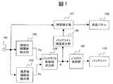
図1は、本発明による液晶表示装置の第1の実施例を示すブロック図である。
液晶表示装置は、映像入力部101と、領域内階調値検出部102と、境界部階調値検出部103と、バックライト制御値決定部104と、バックライト制御部105と、バックライト輝度算出部106、映像補正部107と、液晶パネル108、バックライト109を備えて構成される。液晶パネル108は、入力映像信号の階調レベルに応じて画素の透過率を制御し、バックライト109は液晶パネル108を背面から照射する。バックライト109はLED等からなる複数の光源ブロックで構成し、それぞれの光源ブロックは異なる明るさ(バックライト輝度)で点灯することが可能である。FIG. 1 is a block diagram showing a first embodiment of a liquid crystal display device according to the present invention.
The liquid crystal display device includes a
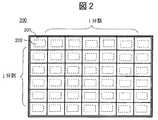
始めに、液晶パネル108の画面の領域分割について説明する。
図2は、表示画面の領域分割を示す図である。表示画面200上の画素は複数の画素群からなるサブ領域201に分割される。ここでは、画面横方向にi分割、画面縦方向にj分割し、i×j個の矩形状のサブ領域201に分割している。各サブ領域201は、それぞれ光源ブロック202を備え、各光源ブロック202は独立に明るさの制御が可能である。なお、1個のサブ領域201が複数の光源ブロック202により照射される構成とすることもできる。First, the screen area division of the
FIG. 2 is a diagram showing area division of the display screen. Pixels on the
ここで図9は、各光源ブロック202の一構成例を示す図である。光源ブロック202のそれぞれは、一次光源としての例えば発光ダイオード(LED)901が、LED駆動基板902の一方の面(液晶パネル906側の面)に実装されている。一方、LED駆動基板902の他方の面には、LED901に駆動電流を供給するためのLEDドライバ907が実装されており、このLEDドライバ907からLED901へ供給される駆動電流が上記バックライト制御部105により制御される。ここで、LED901は、例えば白色光を出射するものであり、またLEDの電極面に対して水平方向(この例ではLED駆動基板902の主平面と平行な方向と等しい)に光を出射する、いわゆるサイドビュー型のLEDを用いている。 Here, FIG. 9 is a diagram illustrating a configuration example of each
このLED901の光出射側には、LED901からの出射光(図9中では点線の矢印で示している)を前面側(液晶パネル906側)に導く導光板904が配置されている。ここで、LED901は、1枚の導光板904に対し複数個(例えば3個)用いられており、ここでは、複数のLED901が紙面と直交する方向に一列に配列されているものとする。また導光板ブロック904の背面側には、導光板904に入射されたLED901からの出射光を効率的に前面側に反射させるための反射シート903が設けられている。また反射シート903とLED駆動基板902との間の空間には、光の反射のために白色にされた支持部材909が配置されており、この支持部材909により反射シート903及び導光板904をその背面側から支持する。 A
導光板904は、液晶パネル906の垂直方向(図9の紙面左右方向)の断面が、図9に示されるように光が入射される入射端面から、その入射端面と対向する先端部にかけて次第に厚さが薄くなる楔形の形状をなしている。更に導光板904の背面側には反射シート903が設けられている。このため、導光板904に入射したLED901からの出射光は上記した導光板904の楔形の形状、及び反射シート903の反射作用により導光板904内部で上方向(液晶パネル906側の方向)に屈曲される。さらに、導光板904の底面(反射シート903側の面)あるいは光出射面(液晶パネル906側の面)に設けられた拡散反射パターンの作用によって、入射光輝度レベルがほぼ均一な面状の光として、例えば図9の点線の矢印で示されるように、上方(液晶パネル906側の方向)に出射される。 The
拡散板905は、導光板904から出射された光を拡散してさらに空間的に均一な面状の光として液晶パネル906に出射する。液晶パネル906は、入力映像信号に基づきピクセル毎に光透過率が制御され、拡散版905からの光を空間的に変調して映像を形成する。これにより、図中の紙面上方を向かう矢印に示す映像光が液晶表示装置の前面側に出力される。 The
この例では、LED101として白色光を出射するLEDを用いたが、これに限定されるものではなく、例えば赤、青、緑の三色の光をそれぞれ放出する3つのLEDの組を複数用いてもよい。 In this example, an LED that emits white light is used as the
このような構成の光源ブロック202が、液晶パネルの背面において画面の水平及び垂直方向に二次元状に複数配列されている。そして、各光源ブロック202に対してそれぞれ設けられているLED101(ここでは3個一組)を個別に制御することで、サブ領域201の明るさを独立して制御可能にされている。 A plurality of light source blocks 202 having such a configuration are arranged two-dimensionally in the horizontal and vertical directions of the screen on the back surface of the liquid crystal panel. The brightness of the
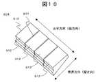
図10は、導光板904の一構成例を示す図である。1つの光源ブロック202に対して1つの導光板を用いてもよいが、例えば図10に示されるように、画面水平方向(横方向、図9の奥行き方向と等しい)に複数(図10では4個)の導光板を結合して一体化し、4つの光源ブロック202に対して1つの一体型導光板910を用いるようにしてもよい。この一体型導光板910を画面水平方向及び垂直方向に複数配列することで液晶パネル全面をカバーする導光板を構成する。このとき、一体化導光板910には画面垂直方向に延びる溝911が形成されており、これにより一体化導光板910が、それぞれが光源ブロック202に対応する複数の導光板ブロック912に分割される。これとは逆に、図示しないが、画面垂直方向に複数の導光板を結合して一体化してもよい。 FIG. 10 is a diagram illustrating a configuration example of the
図3は、表示画面の各サブ領域の領域境界部を示す図である。ここで、サブ領域201は、縦方向の境界線301と横方向の境界線302で囲まれている。そして、サブ領域内を、境界線から離れた中央部304と、境界線に接する領域境界部305(以下、単に境界部とも言う)とに分ける。ここで境界部305とは、各境界線から領域内側に例えば1〜2画素の幅に含まれる枠状の領域である。また、中央部304と境界部305を含む領域を領域内303と呼ぶ。 FIG. 3 is a diagram illustrating a region boundary portion of each sub-region of the display screen. Here, the
次に、各部の動作を説明する。
領域内階調値検出部102は、液晶パネルを構成する複数のサブ領域201毎に、領域内303に属する画素群について入力映像信号の階調レベルを検出し、検出結果から階調レベルの領域内ヒストグラム(頻度表)を作成する。そして、サブ領域201内で最も明るい階調レベルから上位所定範囲(m%)内の画素の階調レベルを除去して、残りの階調レベルのうちで最も明るい階調レベルを求め、領域内最大階調レベルPaとする。Next, the operation of each unit will be described.
The in-region tone
境界部階調値検出部103は、液晶パネルを構成する複数のサブ領域201毎に、当該サブ領域内の境界部305に属する画素群について入力映像信号の階調レベルを検出し、検出結果から階調レベルの境界部ヒストグラム(頻度表)を作成する。そして、境界部305内で最も明るい階調レベルから上位所定範囲(n%)内の画素の階調レベルを除去して、残りの階調レベルのうちで最も明るい階調レベルを求め、境界部最大階調レベルPbとする。 The boundary gradation
バックライト制御値決定部104は、各光源ブロック202に対応する制御データをバックライト制御部105に与える制御データ演算部であり、領域内階調値検出部102で検出された領域内最大階調レベルPaと、境界部階調値検出部103で検出された境界部最大階調レベルPbとを比較し、階調レベルの大きい方を当該サブ領域201の最大階調レベルPcとして決定する。そして、決定した最大階調レベルPcと階調レベルの上限値Pmaxとの比から当該サブ領域201に対するバックライト制御値Kを求める。
K=Pc/Pmax(K≦1)
また、バックライト制御値Kによりバックライトの輝度Bを、
B=K×Bmax(Bmaxはバックライトの最大輝度)
に低下させ、バックライトの消費電力を低減する。The backlight control
K = Pc / Pmax (K ≦ 1)
Further, the backlight brightness B is determined by the backlight control value K.
B = K × Bmax (Bmax is the maximum brightness of the backlight)
To reduce the power consumption of the backlight.
バックライト制御部105は、バックライト制御値決定部104で決定した各サブ領域に対するバックライト制御値Kを受け、当該サブ領域に属するバックライト109(光源ブロック)に対して光源(LED)を点灯させるため制御を行う。光源の輝度を調整するため、例えばPWM(Pulse Width Modulation)や振幅変調で制御する。PWMの場合には、輝度最大のときデューティ比を100%になるよう設定し、バックライト制御値Kに応じてデューティ比を変える。また、PWM周波数は、液晶表示装置のフレーム周波数より高いことが望ましい。 The
バックライト輝度算出部106では、バックライト制御値決定部104から送出された各サブ領域に対するバックライト制御値Kに基づき、画面上のバックライト輝度を算出する。画面上の任意の点Aにおけるバックライト輝度Bsumは、各サブ領域のバックライト(光源ブロック)を1つずつ前記バックライト制御値Kで点灯させたときの点Aの輝度を求め、その総和をとることで求める。 The backlight
映像補正部107では、バックライト輝度算出部106で算出されたバックライト輝度Bsumに基づき、各画素の映像信号(階調値)の補正を行う。バックライト輝度Bsumが100%点灯した場合のバックライト輝度をBmax、入力映像信号の補正前の階調値をPinとしたとき、補正後の階調値Poutは、
Pout=Pin×Bmax/Bsum
となるよう補正する。補正された映像信号を液晶パネル108へ送出する。The
Pout = Pin × Bmax / Bsum
Correct so that The corrected video signal is sent to the
液晶パネル部108では、入力された補正後の映像信号に基づいて階調電圧制御信号と駆動制御信号を生成し、パネル上の画素回路へ階調電圧を印加し、当該画素領域における液晶の透過率を制御する。 The liquid
上述した領域内階調知検出部102、境界部階調値検出部103、バックライト制御値決定部104、バックライト制御部105、バックライト輝度算出部106、及び映像補正部107の各要素を例えば集積化し、1つのバックライト制御回路として構成してもよい。このバックライト制御回路は、例えばリモコンからのユーザの指令に応答して液晶表示装置全体を制御するための中央処理装置(CPU)に組み込んでもよいし、またこのCPUとは別のバックライト制御専用のICもしくはLSIとして構成してもよい。 The above-described intra-regional
図1では省略したが、バックライト制御値決定部104の後段には空間フィルタと時間フィルタを挿入しても良い。
空間フィルタは、隣接するサブ領域間での光漏れの影響を考慮してバックライト制御値Kを補正する。すなわち、隣接するサブ領域間での漏れ量を示す領域係数を用いて周囲の領域からの光漏れ量を加算し、当該サブ領域のバックライト輝度が所望の値になるようにバックライト制御値KをK’に補正するものである。Although omitted in FIG. 1, a spatial filter and a temporal filter may be inserted after the backlight control
The spatial filter corrects the backlight control value K in consideration of the influence of light leakage between adjacent sub-regions. That is, the amount of light leakage from surrounding regions is added using a region coefficient indicating the amount of leakage between adjacent subregions, and the backlight control value K is set so that the backlight luminance of the subregions becomes a desired value. Is corrected to K ′.
また時間フィルタは、フリッカ防止用のものである。各サブ領域のバックライト制御値Kを数フレーム分保持しておき、前記空間フィルタで補正された各領域のバックライト制御値K’と比較する。その差分がある閾値よりも大きい場合、バックライト制御値として補正した制御値K’ではなく、保持している制御値Kを僅かに増減させた値で置き換える。 The time filter is for preventing flicker. The backlight control value K of each sub-region is held for several frames and compared with the backlight control value K ′ of each region corrected by the spatial filter. When the difference is larger than a certain threshold value, the control value K ′ corrected as the backlight control value is replaced with a value obtained by slightly increasing or decreasing the held control value K.
本実施例では、サブ領域201内における最大階調レベルPaとともに、サブ領域内の境界部305における最大階調レベルPbを求め、階調レベルの大きい方を最大階調レベルPcとして採用する。よって、階調レベルの大きな画素が境界部305に偏って存在するとき、これを優先して最大階調レベルPcを決定できる。その結果、境界部305における階調つぶれが小さくなり、これに伴う輝度段差を抑えることができる。 In this embodiment, the maximum gradation level Pb at the
図4は、本実施例におけるバックライト制御値の決定方法を示すフローチャートである。各サブ領域201毎に、以下の手順でバックライト制御値Kを決定する。
S401では、入力映像信号に基づいて、領域内303の対象画素の画素値を検出する。そのとき、RGBの各画素値のうちで最大階調の画素値を選択する。その後、選択した画素値をディスプレイの特性に合わせたガンマ変換を行う。なお、ガンマ変換は、後述のヒストグラム作成後の工程(S407〜S409)で行っても良い。FIG. 4 is a flowchart showing a method for determining the backlight control value in this embodiment. For each
In S401, the pixel value of the target pixel in the
S402では、ガンマ変換後の画素値を予め定めた複数の階調レベルに区分する。例えば、最大階調値が255のとき、これを階調幅16で16段階のレベル(後述図5A,図5BにおけるH1〜H16)を設定し、どのレベルに属するかを判定する。
S403では、領域内ヒストグラムにおいて、S402で取得した階調レベルに対する頻度値としてカウントする。In S402, the pixel value after the gamma conversion is divided into a plurality of predetermined gradation levels. For example, when the maximum gradation value is 255, 16 levels (H1 to H16 in FIGS. 5A and 5B described later) are set with a gradation width of 16, and it is determined to which level.
In S403, the frequency is counted as the frequency value for the gradation level acquired in S402 in the in-region histogram.
S404では、対象画素が境界部305に属するかどうかを判定する。境界部305に属していれば、S405へ進み、属していなければ(すなわち中央部304であれば)S406へ進む。
S405では、境界部ヒストグラムにおいて、S402で取得した階調レベルに対する頻度値としてカウントする。
S406では,領域内303の全画素の処理を終了したかどうかを判定する。終了していなければS401へ戻り、残りの対象画素について処理を繰り返す。終了していればS407へ進む。In S404, it is determined whether or not the target pixel belongs to the
In S405, in the boundary part histogram, it counts as a frequency value with respect to the gradation level acquired in S402.
In S406, it is determined whether or not the processing for all the pixels in the
S407では、領域内ヒストグラムを参照し領域内最大階調レベルPaを決定する。領域内ヒストグラムの中で、最も明るい階調レベルから上位所定範囲(m%)内の画素の階調レベルを除去して、残りの階調レベルのうちで最も明るい階調レベルを求め、領域内最大階調レベルPaとする。
S408では、境界部ヒストグラムを参照し境界部最大階調レベルPbを決定する。境界部ヒストグラムの中で、最も明るい階調レベルから上位所定範囲(n%)内の画素の階調レベルを除去して、残りの階調レベルのうちで最も明るい階調レベルを求め、境界部最大階調レベルPbとする。In S407, the intra-region maximum gradation level Pa is determined with reference to the intra-region histogram. In the in-region histogram, the tone level of the pixel in the upper predetermined range (m%) is removed from the brightest tone level, and the brightest tone level is obtained from the remaining tone levels. The maximum gradation level Pa is assumed.
In S408, the boundary portion maximum gradation level Pb is determined with reference to the boundary portion histogram. In the boundary histogram, the gradation level of the pixel within the upper predetermined range (n%) is removed from the brightest gradation level, and the brightest gradation level is obtained from the remaining gradation levels. The maximum gradation level Pb is assumed.
S409では、領域内最大階調レベルPaと境界部最大階調レベルPbとを比較し、階調レベルの大きい方を当該サブ領域の最大階調レベルPcとする。
S410では、最大階調レベルPcと階調レベルの上限値Pmaxとの比Pc/Pmaxを求めて、当該サブ領域201に対するバックライト制御値Kとする。In S409, the region maximum gradation level Pa and the boundary maximum gradation level Pb are compared, and the larger gradation level is set as the maximum gradation level Pc of the sub-region.
In S410, a ratio Pc / Pmax between the maximum gradation level Pc and the gradation level upper limit value Pmax is obtained and set as the backlight control value K for the
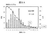
図5Aと図5Bは、作成したヒストグラムの一例を示す図である。
図5Aは領域内ヒストグラムの一例で、階調レベルH1〜H16に対する頻度を示す。また比率とは、各階調レベルにて存在する画素数を最も明るい階調レベルを起点に累積値として示したものである。領域内最大階調レベルPaを求めるには、上記比率が所定範囲、例えばm=3%となる範囲の階調レベル(H16〜H13)を除去する。そして、残りの階調レベルのうちで最も明るい階調レベルであるH12を領域内最大階調レベルPaとする。5A and 5B are diagrams illustrating an example of the created histogram.
FIG. 5A is an example of the in-region histogram and shows the frequency with respect to the gradation levels H1 to H16. The ratio indicates the number of pixels existing at each gradation level as an accumulated value starting from the brightest gradation level. In order to obtain the in-region maximum gradation level Pa, gradation levels (H16 to H13) in a range where the ratio is within a predetermined range, for example, m = 3%, are removed. Then, H12 which is the brightest gradation level among the remaining gradation levels is set as the in-region maximum gradation level Pa.
一方図5Bは境界部ヒストグラムの一例で、同様に階調レベルH1〜H16に対する頻度と比率を示す。境界部の画素数は領域全体の画素数よりはるかに少ないので、母数は小さくなっている。境界部最大階調レベルPbを求めるには、上記比率が所定範囲、例えばn=3%となる範囲の階調レベル(H16〜H14)を除去し、残りの階調レベルのうちで最も明るい階調レベルであるH13を境界部最大階調レベルPbとする。 On the other hand, FIG. 5B is an example of the boundary portion histogram, and similarly shows the frequency and ratio for the gradation levels H1 to H16. Since the number of pixels at the boundary is much smaller than the number of pixels in the entire region, the population parameter is small. In order to obtain the boundary maximum gradation level Pb, gradation levels (H16 to H14) in which the ratio is within a predetermined range, for example, n = 3%, are removed, and the brightest floor among the remaining gradation levels is obtained. The tone level H13 is set as the boundary maximum gradation level Pb.
この場合、領域内最大階調レベルPaはH12、境界部最大階調レベルPbはH13であり、当該サブ領域の最大階調レベルPcとして階調レベルの大きい方であるH13を採用する。これに従い、バックライト制御値Kは、K=Pc/Pmax=H13/H16=0.81と決定する。 In this case, the in-region maximum gradation level Pa is H12, the boundary maximum gradation level Pb is H13, and H13 having the larger gradation level is adopted as the maximum gradation level Pc of the sub-region. Accordingly, the backlight control value K is determined as K = Pc / Pmax = H13 / H16 = 0.81.
なお、領域内ヒストグラムで除去する画素の範囲(m%)と、境界部ヒストグラムで除去する画素の範囲(n%)は、画質劣化の許容値に応じて適宜設定し、またm値とn値を異なる範囲に設定しても良い。 Note that the pixel range (m%) to be removed by the in-region histogram and the pixel range (n%) to be removed by the boundary histogram are appropriately set according to the allowable value of image quality degradation, and the m value and the n value. May be set to different ranges.
本実施例によれば、最も明るい階調レベルから所定範囲のレベルを除去して最大階調レベルPcを決定するので、バックライトの消費電力を大幅に低減することができる。その際、境界部に階調レベルの大きな画素が存在するとき、これを優先して最大階調レベルPcを決定する。よって、図6で示したような境界部603における階調つぶれ614が小さくなり、これに伴う輝度段差615及び影部607の発生を抑えることができる。 According to the present embodiment, since the maximum gradation level Pc is determined by removing a predetermined range of levels from the brightest gradation level, the power consumption of the backlight can be greatly reduced. At this time, when a pixel having a large gradation level exists at the boundary, the maximum gradation level Pc is determined by giving priority to the pixel. Therefore, the
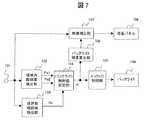
図7は、本発明による液晶表示装置の第2の実施例を示すブロック図である。その構成は前記第1の実施例(図1)を基本としており、同一要素には同一符号を付す。図1と異なる箇所について説明する。 FIG. 7 is a block diagram showing a second embodiment of the liquid crystal display device according to the present invention. The configuration is based on the first embodiment (FIG. 1), and the same elements are denoted by the same reference numerals. A different part from FIG. 1 is demonstrated.
領域内階調値検出部102は、入力映像信号の階調レベルを検出し、検出結果から階調レベルの領域内ヒストグラムを作成する。そして、サブ領域201内で最も明るい階調レベルから2通りの所定範囲(m1%,m2%)内の画素の階調レベルを除去して、残りの階調レベルのうちで最も明るい階調レベルを求め、2通りの領域内最大階調レベルPa1,Pa2を求める。このとき、m1<m2に設定すると、Pa1≧Pa2となる。例えば、m1=1%、m2=3%などとする。 The in-region gradation
境界部階調値検出部103は、図1と同様に境界部最大階調レベルPbを求める。バックライト制御値決定部104は、領域内階調値検出部102で求めた2通りの領域内最大階調レベルPa1,Pa2を入力し、境界部階調値検出部103から入力する境界部最大階調レベルPbに基づき、領域内最大階調レベルPa1,Pa2の一方を選択する。すなわち、PbがPa2よりも大きいときは階調レベルが大きい方のPa1を選択し、PbがPa2よりも小さいときは階調レベルが小さい方のPa2を選択して最大階調レベルPcとする。 The boundary gradation
本実施例によれば、境界部に階調レベルの大きな画素が存在するとき、ヒストグラムの上位から除去される範囲が狭くなるので(m1%を採用)、境界部における階調つぶれが小さくなり、これに伴う輝度段差の発生を抑えることができる。 According to the present embodiment, when a pixel having a large gradation level exists in the boundary portion, the range removed from the upper part of the histogram is narrowed (adopting m1%), so the gradation collapse in the boundary portion is reduced, It is possible to suppress the occurrence of a luminance step accompanying this.
図8は、本発明による液晶表示装置の第3の実施例を示すブロック図である。その構成は前記第1の実施例(図1)を基本としており、同一要素には同一符号を付す。図1と異なる箇所について説明する。 FIG. 8 is a block diagram showing a third embodiment of the liquid crystal display device according to the present invention. The configuration is based on the first embodiment (FIG. 1), and the same elements are denoted by the same reference numerals. A different part from FIG. 1 is demonstrated.
領域内階調値検出部102は、図1と同様に領域内最大階調レベルPaを求める。境界部階調値検出部103は、図1と同様に境界部最大階調レベルPbを求める。 The in-region gradation
新たに設けた境界部階調値比較部110は、境界部階調値検出部102が検出対象とする境界部305に属する画素群の階調レベルを、隣接するサブ領域の対向する画素群の階調レベルと比較し、その差分値が閾値よりも大きい画素については検出対象から除外するように境界部階調値検出部103に対しカウント指令信号Scを送る。 The newly provided boundary gradation
すなわち、図3を用いて説明すると、境界部305に属する各画素の階調レベル(Q1,Q2・・・)について、隣接するサブ領域の対向位置にある各画素の階調レベル(Q1’,Q2’・・・)とそれぞれ比較する。階調レベルの差分|Q1−Q1’|,|Q2−Q2’|が閾値以下であれば、カウント指令信号ScをON(実行)、閾値より大きければカウント指令信号ScをOFF(非実行)とする。境界部階調値検出部103は、指令信号Scに従い境界部ヒストグラムへのカウント動作を実行する。閾値は階調レベルのダイナミックレンジ(上限値と下限値の差分)の例えば3%以下となるように設定する。 That is, with reference to FIG. 3, with respect to the gradation levels (Q1, Q2,...) Of each pixel belonging to the
本実施例によれば、境界部階調値検出部103は、境界線の両側の階調レベルが近接している画素についてのみ境界部ヒストグラムへのカウントを行うことになる。輝度段差は、境界両側の輝度が近接している場合に目立ちやすいので、輝度段差の発生をより確実に抑える効果がある。 According to the present embodiment, the boundary gradation
なお、上記本発明の実施形態の説明においては、サブ領域毎に、サブ領域内全体の最大階調レベルPaとこのサブ領域の隣接サブ領域との境界部の最大階調レベルPbを求めたが、これに限られるものではない。例えば、サブ領域の境界部の階調レベルとこの境界部を除く中央部の最大階調レベルとを求めるようにしてもよい。また、サブ領域内全体のヒストグラムを求め、これから中央部のヒストグラムを除くことにより、境界部の最大階調レベルを求めるようにしてもよい。すなわち、あるサブ領域を全体的に見たとき(すなわち境界部を除く中央部もしくは該中央部を含むサブ領域全体)の最大階調レベルと、そのサブ領域の境界部における最大階調レベルを求めることができるならば、どのような方法を用いてもよい。 In the above description of the embodiment of the present invention, for each sub-region, the maximum gradation level Pa in the entire sub-region and the maximum gradation level Pb at the boundary between adjacent sub-regions of this sub-region are obtained. However, it is not limited to this. For example, the gradation level at the boundary portion of the sub-region and the maximum gradation level at the central portion excluding the boundary portion may be obtained. Further, the maximum gradation level of the boundary portion may be obtained by obtaining a histogram of the entire sub-region and removing the histogram of the central portion from this. That is, the maximum gradation level when a certain sub-region is viewed as a whole (that is, the central portion excluding the boundary portion or the entire sub-region including the central portion) and the maximum gradation level at the boundary portion of the sub-region are obtained. Any method can be used as long as it can.
101…映像入力部、
102…領域内階調値検出部、
103…境界部階調値検出部、
104…バックライト制御値決定部、
105…バックライト制御部、
106…バックライト輝度算出部、
107…映像補正部、
108,906…液晶パネル、
109…バックライト、
110…境界部階調値比較部、
200…表示画面、
201…サブ領域、
202…光源ブロック、
303…領域内、
305…領域境界部、
613,614…階調つぶれ、
615…輝度段差、
901…発光ダイオード(LED)、
904…導光板、
Pa…領域内最大階調レベル、
Pb…境界部最大階調レベル、
Pc…最大階調レベル、
K…バックライト制御値。101 ... Video input section,
102... In-region gradation value detection unit,
103 ... boundary gradation value detection unit,
104 ... Backlight control value determination unit,
105 ... Backlight control unit,
106: Backlight luminance calculation unit,
107 ... image correction unit,
108,906 ... Liquid crystal panel,
109 ... Backlight,
110 ... Boundary tone value comparison unit,
200 ... display screen,
201 ... sub-region,
202 ... light source block,
303 ... in the area,
305 ... area boundary,
613, 614 ... gradation collapse,
615: Luminance step,
901 ... Light emitting diode (LED),
904 ... Light guide plate,
Pa: Maximum gradation level in the area,
Pb: Maximum gradation level at the boundary,
Pc: maximum gradation level,
K: Backlight control value.
Claims (8)
Translated fromJapanese前記液晶パネルはパネル上の画素を複数の画素群からなるサブ領域に分割され、前記バックライトは該サブ領域に対応した複数の光源ブロックで構成されており、
該光源ブロックを個別に制御するためのバックライト制御回路を備え、該制御回路は、
前記各サブ領域において、隣接サブ領域との境界部における入力映像信号から第1最大階調レベルと、前記境界部以外の部分または当該サブ領域における入力映像信号から第2最大階調レベルを求め、
前記第1最大階調レベルと前記第2最大階調レベルのいずれか大きい方を用いて前記各光源ブロックの制御データを演算して各光源ブロックの明るさを個別に制御することを特徴とする液晶表示装置。In a liquid crystal display device comprising a liquid crystal panel that controls the transmittance of pixels according to the gradation level of an input video signal, and a backlight that illuminates the liquid crystal panel from the back side,
The liquid crystal panel divides pixels on the panel into sub-regions composed of a plurality of pixel groups, and the backlight includes a plurality of light source blocks corresponding to the sub-regions,
A backlight control circuit for individually controlling the light source block, the control circuit,
In each of the sub-regions, a first maximum gradation level is obtained from an input video signal at a boundary portion with an adjacent sub-region, and a second maximum gradation level is obtained from an input video signal in a portion other than the boundary portion or the sub-region,
The brightness of each light source block is individually controlled by calculating control data of each light source block using the larger one of the first maximum gradation level and the second maximum gradation level. Liquid crystal display device.
前記液晶パネルはパネル上の画素を複数の画素群からなるサブ領域に分割され、前記バックライトは該サブ領域に対応した複数の光源ブロックで構成されるものであって、
該サブ領域毎に入力映像信号の階調レベルを検出し、該サブ領域内で最も明るい階調レベルから上位所定範囲(m%)内の画素の階調レベルを除去して領域内最大階調レベルPaを検出する領域内階調値検出部と、
該サブ領域内の領域境界部に属する画素群について、最も明るい階調レベルから上位所定範囲(n%)内の画素の階調レベルを除去して境界部最大階調レベルPbを検出する境界部階調値検出部と、
前記領域内最大階調レベルPaと前記境界部最大階調レベルPbのいずれか大きい方を当該サブ領域の最大階調レベルPcに選択し、該最大階調レベルPcと階調レベル上限値Pmaxとの比からバックライト制御値Kを決定するバックライト制御値決定部と、
当該サブ領域を照射する光源ブロックに対して、前記バックライト制御値Kに基づくバックライト輝度で点灯制御するバックライト制御部とを備えたことを特徴とする液晶表示装置。In a liquid crystal display device comprising a liquid crystal panel that controls the transmittance of pixels according to the gradation level of an input video signal, and a backlight that illuminates the liquid crystal panel from the back side,
The liquid crystal panel divides pixels on the panel into sub-regions composed of a plurality of pixel groups, and the backlight is composed of a plurality of light source blocks corresponding to the sub-regions,
The gradation level of the input video signal is detected for each sub-region, and the gradation level of the pixels within the upper predetermined range (m%) is removed from the brightest gradation level in the sub-region, and the maximum gradation in the region An in-region gradation value detection unit for detecting level Pa;
Boundary portion for detecting the boundary maximum gradation level Pb by removing the gradation level of the pixels in the upper predetermined range (n%) from the brightest gradation level for the pixel group belonging to the region boundary in the sub-region A gradation value detector;
The larger of the in-region maximum gradation level Pa and the boundary maximum gradation level Pb is selected as the maximum gradation level Pc of the sub-region, and the maximum gradation level Pc and the gradation level upper limit value Pmax are selected. A backlight control value determining unit that determines a backlight control value K from the ratio of
A liquid crystal display device comprising: a backlight control unit that controls lighting with a backlight luminance based on the backlight control value K with respect to a light source block that irradiates the sub-region.
前記液晶パネルはパネル上の画素を複数の画素群からなるサブ領域に分割され、前記バックライトは該サブ領域に対応した複数の光源ブロックで構成されるものであって、
該サブ領域毎に入力映像信号の階調レベルを検出し、該サブ領域内で最も明るい階調レベルから2通りの所定範囲(m1%,m2%)内の画素の階調レベルを除去して2通りの領域内最大階調レベルPa1,Pa2を検出する領域内階調値検出部と、
該サブ領域内の領域境界部に属する画素群について、最も明るい階調レベルから上位所定範囲(n%)内の画素の階調レベルを除去して境界部最大階調レベルPbを検出する境界部階調値検出部と、
前記境界部最大階調レベルPbに基づき、前記領域内最大階調レベルPa1,Pa2の一方を当該サブ領域の最大階調レベルPcに選択し、該最大階調レベルPcと階調レベル上限値Pmaxとの比からバックライト制御値Kを決定するバックライト制御値決定部と、
当該サブ領域を照射する光源ブロックに対して、前記バックライト制御値Kに基づくバックライト輝度で点灯制御するバックライト制御部とを備えたことを特徴とする液晶表示装置。In a liquid crystal display device comprising a liquid crystal panel that controls the transmittance of pixels according to the gradation level of an input video signal, and a backlight that illuminates the liquid crystal panel from the back side,
The liquid crystal panel divides pixels on the panel into sub-regions composed of a plurality of pixel groups, and the backlight is composed of a plurality of light source blocks corresponding to the sub-regions,
The gradation level of the input video signal is detected for each sub area, and the gradation levels of pixels in two predetermined ranges (m1%, m2%) are removed from the brightest gradation level in the sub area. An in-region gradation value detection unit for detecting two in-region maximum gradation levels Pa1, Pa2,
Boundary portion for detecting the boundary maximum gradation level Pb by removing the gradation level of the pixels in the upper predetermined range (n%) from the brightest gradation level for the pixel group belonging to the region boundary in the sub-region A gradation value detector;
Based on the boundary maximum gradation level Pb, one of the maximum gradation levels Pa1 and Pa2 in the region is selected as the maximum gradation level Pc of the sub-region, and the maximum gradation level Pc and the gradation level upper limit value Pmax are selected. A backlight control value determining unit that determines the backlight control value K from the ratio of
A liquid crystal display device comprising: a backlight control unit that controls lighting with a backlight luminance based on the backlight control value K with respect to a light source block that irradiates the sub-region.
前記境界部階調値検出部が検出対象とする領域境界部に属する画素群の階調レベルを、隣接するサブ領域の対向する画素群の階調レベルと比較し、その差分値が閾値よりも大きい画素については検出対象から除外する境界部階調値比較部を備えたことを特徴とする液晶表示装置。The liquid crystal display device according to claim 3.
The gradation value of the pixel group belonging to the region boundary part to be detected by the boundary gradation value detection unit is compared with the gradation level of the opposing pixel group of the adjacent sub-region, and the difference value is smaller than the threshold value. A liquid crystal display device comprising a boundary tone value comparison unit that excludes large pixels from detection targets.
前記液晶パネルはパネル上の画素を複数の画素群からなるサブ領域に分割され、前記バックライトは該サブ領域に対応した複数の光源ブロックで構成されるものであって、
該サブ領域毎に入力映像信号の階調レベルを検出し、該サブ領域内で最も明るい階調レベルから上位所定範囲(m%)内の画素の階調レベルを除去して領域内最大階調レベルPaを検出し、
該サブ領域内の領域境界部に属する画素群について、最も明るい階調レベルから上位所定範囲(n%)内の画素の階調レベルを除去して境界部最大階調レベルPbを検出し、
前記領域内最大階調レベルPaと前記境界部最大階調レベルPbのいずれか大きい方を当該サブ領域の最大階調レベルPcに選択し、該最大階調レベルPcと階調レベル上限値Pmaxとの比からバックライト制御値Kを決定し、
当該サブ領域を照射する光源ブロックに対して、前記バックライト制御値Kに基づくバックライト輝度で点灯制御することを特徴とするバックライト制御方法。In a backlight control method of a liquid crystal display device including a backlight that irradiates a liquid crystal panel from the back side,
The liquid crystal panel divides pixels on the panel into sub-regions composed of a plurality of pixel groups, and the backlight is composed of a plurality of light source blocks corresponding to the sub-regions,
The gradation level of the input video signal is detected for each sub-region, and the gradation level of the pixels within the upper predetermined range (m%) is removed from the brightest gradation level in the sub-region, and the maximum gradation in the region Detect level Pa,
For the pixel group belonging to the region boundary in the sub-region, the boundary maximum gradation level Pb is detected by removing the gradation level of the pixels in the upper predetermined range (n%) from the brightest gradation level,
The larger of the in-region maximum gradation level Pa and the boundary maximum gradation level Pb is selected as the maximum gradation level Pc of the sub-region, and the maximum gradation level Pc and the gradation level upper limit value Pmax are selected. The backlight control value K is determined from the ratio of
A backlight control method, wherein lighting control is performed on a light source block that irradiates the sub-region with backlight luminance based on the backlight control value K.
前記液晶パネルはパネル上の画素を複数の画素群からなるサブ領域に分割され、前記バックライトは該サブ領域に対応した複数の光源ブロックで構成されるものであって、
該サブ領域毎に入力映像信号の階調レベルを検出し、該サブ領域内で最も明るい階調レベルから2通りの所定範囲(m1%,m2%)内の画素の階調レベルを除去して2通りの領域内最大階調レベルPa1,Pa2を検出し、
該サブ領域内の領域境界部に属する画素群について、最も明るい階調レベルから上位所定範囲(n%)内の画素の階調レベルを除去して境界部最大階調レベルPbを検出し、
前記境界部最大階調レベルPbに基づき、前記領域内最大階調レベルPa1,Pa2の一方を当該サブ領域の最大階調レベルPcに選択し、該最大階調レベルPcと階調レベル上限値Pmaxとの比からバックライト制御値Kを決定し、
当該サブ領域を照射する光源ブロックに対して、前記バックライト制御値Kに基づくバックライト輝度で点灯制御することを特徴とするバックライト制御方法。In a backlight control method of a liquid crystal display device including a backlight that irradiates a liquid crystal panel from the back side,
The liquid crystal panel divides pixels on the panel into sub-regions composed of a plurality of pixel groups, and the backlight is composed of a plurality of light source blocks corresponding to the sub-regions,
The gradation level of the input video signal is detected for each sub area, and the gradation levels of pixels in two predetermined ranges (m1%, m2%) are removed from the brightest gradation level in the sub area. Detect maximum gradation levels Pa1 and Pa2 in two areas,
For the pixel group belonging to the region boundary in the sub-region, the boundary maximum gradation level Pb is detected by removing the gradation level of the pixels in the upper predetermined range (n%) from the brightest gradation level,
Based on the boundary maximum gradation level Pb, one of the maximum gradation levels Pa1 and Pa2 in the region is selected as the maximum gradation level Pc of the sub-region, and the maximum gradation level Pc and the gradation level upper limit value Pmax are selected. The backlight control value K is determined from the ratio of
A backlight control method, wherein lighting control is performed on a light source block that irradiates the sub-region with backlight luminance based on the backlight control value K.
前記境界部最大階調レベルPbを検出する際、前記領域境界部に属する画素群の階調レベルを隣接するサブ領域の対向する画素群の階調レベルと比較し、その差分値が閾値よりも大きい画素については検出対象から除外することを特徴とするバックライト制御方法。The backlight control method according to claim 6,
When the boundary maximum gradation level Pb is detected, the gradation level of the pixel group belonging to the region boundary is compared with the gradation level of the opposing pixel group in the adjacent sub-region, and the difference value is smaller than the threshold value. A backlight control method, wherein large pixels are excluded from detection targets.
Priority Applications (4)
| Application Number | Priority Date | Filing Date | Title |
|---|---|---|---|
| JP2009205844AJP2011059177A (en) | 2009-09-07 | 2009-09-07 | Liquid crystal display device and backlight control method |
| EP10250960AEP2306445A1 (en) | 2009-09-07 | 2010-05-21 | Liquid crystal display device and backlight control method |
| US12/785,242US20110057961A1 (en) | 2009-09-07 | 2010-05-21 | Liquid Crystal Display Device and Backlight Control Method |
| CN2010102428951ACN102013239A (en) | 2009-09-07 | 2010-07-30 | Liquid crystal display device and backlight control method |
Applications Claiming Priority (1)
| Application Number | Priority Date | Filing Date | Title |
|---|---|---|---|
| JP2009205844AJP2011059177A (en) | 2009-09-07 | 2009-09-07 | Liquid crystal display device and backlight control method |
Publications (1)
| Publication Number | Publication Date |
|---|---|
| JP2011059177Atrue JP2011059177A (en) | 2011-03-24 |
Family
ID=42498730
Family Applications (1)
| Application Number | Title | Priority Date | Filing Date |
|---|---|---|---|
| JP2009205844AWithdrawnJP2011059177A (en) | 2009-09-07 | 2009-09-07 | Liquid crystal display device and backlight control method |
Country Status (4)
| Country | Link |
|---|---|
| US (1) | US20110057961A1 (en) |
| EP (1) | EP2306445A1 (en) |
| JP (1) | JP2011059177A (en) |
| CN (1) | CN102013239A (en) |
Cited By (6)
| Publication number | Priority date | Publication date | Assignee | Title |
|---|---|---|---|---|
| WO2013018472A1 (en)* | 2011-08-04 | 2013-02-07 | シャープ株式会社 | Image display device |
| WO2013018822A1 (en)* | 2011-08-03 | 2013-02-07 | シャープ株式会社 | Image display device and image display method |
| JP2013029573A (en)* | 2011-07-27 | 2013-02-07 | Hitachi Consumer Electronics Co Ltd | Image display apparatus |
| WO2013080287A1 (en)* | 2011-11-28 | 2013-06-06 | 日立コンシューマエレクトロニクス株式会社 | Image display device, and display method for image display device |
| JP2022132061A (en)* | 2021-02-26 | 2022-09-07 | 日亜化学工業株式会社 | Image display method |
| US11837181B2 (en) | 2021-02-26 | 2023-12-05 | Nichia Corporation | Color balancing in display of multiple images |
Families Citing this family (24)
| Publication number | Priority date | Publication date | Assignee | Title |
|---|---|---|---|---|
| JP5744586B2 (en)* | 2011-03-24 | 2015-07-08 | キヤノン株式会社 | Liquid crystal display device and program used therefor |
| CN103135737A (en)* | 2011-11-23 | 2013-06-05 | 中兴通讯股份有限公司 | Terminal and method reducing terminal power consumption |
| JP6051544B2 (en)* | 2012-03-13 | 2016-12-27 | セイコーエプソン株式会社 | Image processing circuit, liquid crystal display device, electronic apparatus, and image processing method |
| JP5498532B2 (en)* | 2012-05-23 | 2014-05-21 | シャープ株式会社 | Video display device |
| WO2013188298A2 (en) | 2012-06-15 | 2013-12-19 | Dolby Laboratories Licensing Corporation | Systems and methods for controlling dual modulation displays |
| JP5929538B2 (en) | 2012-06-18 | 2016-06-08 | セイコーエプソン株式会社 | Display control circuit, display control method, electro-optical device, and electronic apparatus |
| KR102053618B1 (en)* | 2013-04-11 | 2019-12-09 | 엘지디스플레이 주식회사 | Electronic device, display controlling apparatus and method there of |
| CN103676254B (en)* | 2013-12-04 | 2017-02-08 | 青岛海信电器股份有限公司 | See-through display device and driving method thereof, and electronic equipment |
| JP6463118B2 (en)* | 2014-12-19 | 2019-01-30 | キヤノン株式会社 | VIDEO SIGNAL GENERATION DEVICE, LIQUID CRYSTAL DISPLAY DEVICE, VIDEO SIGNAL GENERATION METHOD, AND VIDEO SIGNAL GENERATION PROGRAM |
| CN104505055B (en)* | 2014-12-31 | 2017-02-22 | 深圳创维-Rgb电子有限公司 | Method and device for adjusting backlight brightness |
| US9805662B2 (en)* | 2015-03-23 | 2017-10-31 | Intel Corporation | Content adaptive backlight power saving technology |
| CN105137627A (en)* | 2015-09-22 | 2015-12-09 | 青岛海信电器股份有限公司 | Method and device for partition backlight detection |
| US10916191B2 (en)* | 2017-02-13 | 2021-02-09 | Samsung Display Co., Ltd. | Display device and method of driving the same |
| CN106710534A (en)* | 2017-02-28 | 2017-05-24 | 青岛海信电器股份有限公司 | Subregion backlight gain coefficient determination method and device and liquid crystal display device |
| CN107610675A (en)* | 2017-09-11 | 2018-01-19 | 青岛海信电器股份有限公司 | A kind of image processing method and device based on dynamic level |
| CN107665681B (en)* | 2017-09-26 | 2020-06-05 | 武汉华星光电技术有限公司 | Liquid crystal display driving method, system and computer readable medium |
| CN110308576B (en)* | 2019-08-01 | 2024-04-12 | 深圳市鑫三力自动化设备有限公司 | Mechanism for improving brightness performance consistency of assembled liquid crystal display and backlight module |
| CN111477186B (en)* | 2020-05-07 | 2021-03-16 | Tcl华星光电技术有限公司 | Time schedule controller, display panel and driving method thereof |
| US12002432B2 (en)* | 2020-05-29 | 2024-06-04 | Nichia Corporation | Information processing method, information processing program, information processing device, and image display device |
| KR102696842B1 (en)* | 2020-12-14 | 2024-08-19 | 엘지디스플레이 주식회사 | Electroluminescent Display Device And Driving Method Of The Same |
| US11972739B2 (en)* | 2021-02-26 | 2024-04-30 | Nichia Corporation | Luminance control of backlight in display of image |
| CN114420059B (en)* | 2021-12-31 | 2023-12-12 | 海宁奕斯伟集成电路设计有限公司 | Backlight control method and device and display equipment |
| CN114663682B (en)* | 2022-03-18 | 2023-04-07 | 北京理工大学 | Target significance detection method for improving anti-interference performance |
| JP2024027865A (en)* | 2022-08-19 | 2024-03-01 | 株式会社ジャパンディスプレイ | display device |
Family Cites Families (9)
| Publication number | Priority date | Publication date | Assignee | Title |
|---|---|---|---|---|
| TWI249630B (en)* | 1999-05-10 | 2006-02-21 | Matsushita Electric Industrial Co Ltd | Image display device and method for displaying image |
| JP4348457B2 (en)* | 2002-03-13 | 2009-10-21 | ドルビー ラボラトリーズ ライセンシング コーポレイション | High dynamic range display, display controller, and image display method |
| KR100989159B1 (en)* | 2003-12-29 | 2010-10-20 | 엘지디스플레이 주식회사 | LCD and its control method |
| KR101097512B1 (en)* | 2004-11-23 | 2011-12-22 | 엘지디스플레이 주식회사 | Liquid crystal dispaly apparatus and driviing method thereof |
| JP4904783B2 (en)* | 2005-03-24 | 2012-03-28 | ソニー株式会社 | Display device and display method |
| JP5256552B2 (en)* | 2006-07-10 | 2013-08-07 | Nltテクノロジー株式会社 | Liquid crystal display device, drive control circuit used for the liquid crystal display device, and drive method |
| US20080042927A1 (en)* | 2006-08-16 | 2008-02-21 | Samsung Electronics Co., Ltd. | Display apparatus and method of adjusting brightness thereof |
| CN101523477A (en)* | 2006-11-20 | 2009-09-02 | 夏普株式会社 | Display apparatus driving method, driver circuit, liquid crystal display apparatus, and television receiver |
| CN101363994B (en)* | 2007-08-08 | 2011-09-07 | 深圳Tcl新技术有限公司 | Lcd device and method |
- 2009
- 2009-09-07JPJP2009205844Apatent/JP2011059177A/ennot_activeWithdrawn
- 2010
- 2010-05-21USUS12/785,242patent/US20110057961A1/ennot_activeAbandoned
- 2010-05-21EPEP10250960Apatent/EP2306445A1/ennot_activeWithdrawn
- 2010-07-30CNCN2010102428951Apatent/CN102013239A/enactivePending
Cited By (8)
| Publication number | Priority date | Publication date | Assignee | Title |
|---|---|---|---|---|
| JP2013029573A (en)* | 2011-07-27 | 2013-02-07 | Hitachi Consumer Electronics Co Ltd | Image display apparatus |
| WO2013018822A1 (en)* | 2011-08-03 | 2013-02-07 | シャープ株式会社 | Image display device and image display method |
| WO2013018472A1 (en)* | 2011-08-04 | 2013-02-07 | シャープ株式会社 | Image display device |
| JP2013050703A (en)* | 2011-08-04 | 2013-03-14 | Sharp Corp | Video display device |
| US9001166B2 (en) | 2011-08-04 | 2015-04-07 | Sharp Kabushiki Kaisha | Video display device |
| WO2013080287A1 (en)* | 2011-11-28 | 2013-06-06 | 日立コンシューマエレクトロニクス株式会社 | Image display device, and display method for image display device |
| JP2022132061A (en)* | 2021-02-26 | 2022-09-07 | 日亜化学工業株式会社 | Image display method |
| US11837181B2 (en) | 2021-02-26 | 2023-12-05 | Nichia Corporation | Color balancing in display of multiple images |
Also Published As
| Publication number | Publication date |
|---|---|
| US20110057961A1 (en) | 2011-03-10 |
| EP2306445A1 (en) | 2011-04-06 |
| CN102013239A (en) | 2011-04-13 |
Similar Documents
| Publication | Publication Date | Title |
|---|---|---|
| JP2011059177A (en) | Liquid crystal display device and backlight control method | |
| JP5337757B2 (en) | Liquid crystal display device and backlight control method | |
| EP2390871B1 (en) | Control of a back light of a liquid crystal device | |
| JP4968219B2 (en) | Liquid crystal display device and video display method used therefor | |
| JP5460435B2 (en) | Image display device and control method of image display device | |
| US9607577B2 (en) | Dynamic power and brightness control for a display screen | |
| KR101231445B1 (en) | Display device and display method | |
| KR100885285B1 (en) | Liquid crystal display and image display method used therein | |
| JP2008304907A (en) | Liquid crystal display, and image display method used therefor | |
| JP2010175913A (en) | Image display apparatus | |
| JP2010044180A (en) | Liquid crystal display device and video signal processing method used for the same | |
| JP2012123100A (en) | Liquid crystal display device | |
| JP2009042652A (en) | Liquid crystal display device and image display method thereof | |
| KR102119091B1 (en) | Display device and driving method thereof | |
| JP2009042651A (en) | Liquid crystal display device and image display method thereof | |
| JP2009042650A (en) | Liquid crystal display device and image display method thereof | |
| JP5743782B2 (en) | Image display device | |
| JP5002725B2 (en) | Backlight device and backlight control method | |
| JP5176896B2 (en) | Liquid crystal display | |
| JP5111652B2 (en) | Backlight device and control method of backlight device | |
| JP2012095127A (en) | Video display device and backlight control device | |
| JP2013008678A (en) | Lighting device, image display device, and image signal control method |
Legal Events
| Date | Code | Title | Description |
|---|---|---|---|
| A621 | Written request for application examination | Free format text:JAPANESE INTERMEDIATE CODE: A621 Effective date:20120322 | |
| A977 | Report on retrieval | Free format text:JAPANESE INTERMEDIATE CODE: A971007 Effective date:20121009 | |
| A761 | Written withdrawal of application | Free format text:JAPANESE INTERMEDIATE CODE: A761 Effective date:20121108 |