JP2011054637A - Semiconductor device and method of manufacturing the same - Google Patents
Semiconductor device and method of manufacturing the sameDownload PDFInfo
- Publication number
- JP2011054637A JP2011054637AJP2009200117AJP2009200117AJP2011054637AJP 2011054637 AJP2011054637 AJP 2011054637AJP 2009200117 AJP2009200117 AJP 2009200117AJP 2009200117 AJP2009200117 AJP 2009200117AJP 2011054637 AJP2011054637 AJP 2011054637A
- Authority
- JP
- Japan
- Prior art keywords
- semiconductor device
- guard ring
- wiring
- insulating film
- integrated circuit
- Prior art date
- Legal status (The legal status is an assumption and is not a legal conclusion. Google has not performed a legal analysis and makes no representation as to the accuracy of the status listed.)
- Pending
Links
- 239000004065semiconductorSubstances0.000titleclaimsabstractdescription211
- 238000004519manufacturing processMethods0.000titleclaimsdescription30
- 239000000758substrateSubstances0.000claimsabstractdescription51
- 239000010949copperSubstances0.000claimsdescription23
- RYGMFSIKBFXOCR-UHFFFAOYSA-NCopperChemical compound[Cu]RYGMFSIKBFXOCR-UHFFFAOYSA-N0.000claimsdescription21
- VYPSYNLAJGMNEJ-UHFFFAOYSA-NSilicium dioxideChemical compoundO=[Si]=OVYPSYNLAJGMNEJ-UHFFFAOYSA-N0.000claimsdescription21
- 229910052802copperInorganic materials0.000claimsdescription21
- 229910052814silicon oxideInorganic materials0.000claimsdescription21
- XAGFODPZIPBFFR-UHFFFAOYSA-NaluminiumChemical compound[Al]XAGFODPZIPBFFR-UHFFFAOYSA-N0.000claimsdescription20
- 229910052782aluminiumInorganic materials0.000claimsdescription20
- WFKWXMTUELFFGS-UHFFFAOYSA-NtungstenChemical compound[W]WFKWXMTUELFFGS-UHFFFAOYSA-N0.000claimsdescription19
- 229910052721tungstenInorganic materials0.000claimsdescription19
- 239000010937tungstenSubstances0.000claimsdescription19
- RTAQQCXQSZGOHL-UHFFFAOYSA-NTitaniumChemical compound[Ti]RTAQQCXQSZGOHL-UHFFFAOYSA-N0.000claimsdescription16
- 229910052715tantalumInorganic materials0.000claimsdescription16
- GUVRBAGPIYLISA-UHFFFAOYSA-Ntantalum atomChemical compound[Ta]GUVRBAGPIYLISA-UHFFFAOYSA-N0.000claimsdescription16
- 239000010936titaniumSubstances0.000claimsdescription16
- 229910052719titaniumInorganic materials0.000claimsdescription16
- 238000000034methodMethods0.000claimsdescription15
- 239000000853adhesiveSubstances0.000claimsdescription11
- 230000001070adhesive effectEffects0.000claimsdescription11
- 229910045601alloyInorganic materials0.000claimsdescription11
- 239000000956alloySubstances0.000claimsdescription11
- 229910021420polycrystalline siliconInorganic materials0.000claimsdescription9
- 229920005591polysiliconPolymers0.000claimsdescription9
- NRTOMJZYCJJWKI-UHFFFAOYSA-NTitanium nitrideChemical compound[Ti]#NNRTOMJZYCJJWKI-UHFFFAOYSA-N0.000claimsdescription8
- 238000005304joiningMethods0.000claimsdescription8
- MZLGASXMSKOWSE-UHFFFAOYSA-Ntantalum nitrideChemical compound[Ta]#NMZLGASXMSKOWSE-UHFFFAOYSA-N0.000claimsdescription8
- 238000010030laminatingMethods0.000claimsdescription4
- ATJFFYVFTNAWJD-UHFFFAOYSA-NTinChemical compound[Sn]ATJFFYVFTNAWJD-UHFFFAOYSA-N0.000claimsdescription3
- PCHJSUWPFVWCPO-UHFFFAOYSA-NgoldChemical compound[Au]PCHJSUWPFVWCPO-UHFFFAOYSA-N0.000claimsdescription3
- 229910052737goldInorganic materials0.000claimsdescription3
- 239000010931goldSubstances0.000claimsdescription3
- 229910052718tinInorganic materials0.000claimsdescription3
- 239000011135tinSubstances0.000claimsdescription3
- 230000002093peripheral effectEffects0.000abstract2
- 239000000463materialSubstances0.000description19
- QVGXLLKOCUKJST-UHFFFAOYSA-Natomic oxygenChemical compound[O]QVGXLLKOCUKJST-UHFFFAOYSA-N0.000description16
- 239000001301oxygenSubstances0.000description16
- 229910052760oxygenInorganic materials0.000description16
- 238000005530etchingMethods0.000description13
- 239000010410layerSubstances0.000description12
- 230000001590oxidative effectEffects0.000description10
- XUIMIQQOPSSXEZ-UHFFFAOYSA-NSiliconChemical compound[Si]XUIMIQQOPSSXEZ-UHFFFAOYSA-N0.000description8
- 239000007789gasSubstances0.000description8
- 229910052710siliconInorganic materials0.000description8
- 239000010703siliconSubstances0.000description8
- 235000012431wafersNutrition0.000description8
- 239000004020conductorSubstances0.000description7
- 238000005260corrosionMethods0.000description7
- 230000007797corrosionEffects0.000description7
- 230000003647oxidationEffects0.000description7
- 238000007254oxidation reactionMethods0.000description7
- 238000005498polishingMethods0.000description6
- 238000000137annealingMethods0.000description5
- 238000001312dry etchingMethods0.000description5
- 230000000149penetrating effectEffects0.000description5
- XKRFYHLGVUSROY-UHFFFAOYSA-NArgonChemical compound[Ar]XKRFYHLGVUSROY-UHFFFAOYSA-N0.000description4
- IJGRMHOSHXDMSA-UHFFFAOYSA-NAtomic nitrogenChemical compoundN#NIJGRMHOSHXDMSA-UHFFFAOYSA-N0.000description4
- 239000004341OctafluorocyclobutaneSubstances0.000description4
- 238000005229chemical vapour depositionMethods0.000description4
- 238000010894electron beam technologyMethods0.000description4
- 238000000227grindingMethods0.000description4
- 238000009413insulationMethods0.000description4
- 239000011229interlayerSubstances0.000description4
- BCCOBQSFUDVTJQ-UHFFFAOYSA-NoctafluorocyclobutaneChemical compoundFC1(F)C(F)(F)C(F)(F)C1(F)FBCCOBQSFUDVTJQ-UHFFFAOYSA-N0.000description4
- 235000019407octafluorocyclobutaneNutrition0.000description4
- 239000000126substanceSubstances0.000description4
- 229910004298SiO 2Inorganic materials0.000description3
- 238000010521absorption reactionMethods0.000description3
- 229910000838Al alloyInorganic materials0.000description2
- 229910018503SF6Inorganic materials0.000description2
- 229910052786argonInorganic materials0.000description2
- UMIVXZPTRXBADB-UHFFFAOYSA-NbenzocyclobuteneChemical compoundC1=CC=C2CCC2=C1UMIVXZPTRXBADB-UHFFFAOYSA-N0.000description2
- 238000010292electrical insulationMethods0.000description2
- SFZCNBIFKDRMGX-UHFFFAOYSA-Nsulfur hexafluorideChemical compoundFS(F)(F)(F)(F)FSFZCNBIFKDRMGX-UHFFFAOYSA-N0.000description2
- 229960000909sulfur hexafluorideDrugs0.000description2
- 238000010586diagramMethods0.000description1
- 230000010354integrationEffects0.000description1
- 239000000203mixtureSubstances0.000description1
- 238000009832plasma treatmentMethods0.000description1
- 230000002265preventionEffects0.000description1
Images


Classifications
- H—ELECTRICITY
- H01—ELECTRIC ELEMENTS
- H01L—SEMICONDUCTOR DEVICES NOT COVERED BY CLASS H10
- H01L2924/00—Indexing scheme for arrangements or methods for connecting or disconnecting semiconductor or solid-state bodies as covered by H01L24/00
- H01L2924/0001—Technical content checked by a classifier
- H01L2924/0002—Not covered by any one of groups H01L24/00, H01L24/00 and H01L2224/00
Landscapes
- Internal Circuitry In Semiconductor Integrated Circuit Devices (AREA)
Abstract
Description
Translated fromJapanese本発明は、半導体装置およびその製造方法に関するものである。 The present invention relates to a semiconductor device and a manufacturing method thereof.
最近の半導体装置の微細化傾向は、さらなる微細化によるマスク工程の高集積化を目指した「more Moore」が減速してきている。それに代わって、垂直方向に素子を積み上げ、その素子間を3次元的に配線で接続することで、素子間の抵抗や容量を低減できる「beyond Moore」が注目を集めている。3次元方向への積層は、ウエハレベルでのパッケージ技術開発が加わることで、低コスト化も可能となる。 The recent trend toward miniaturization of semiconductor devices has slowed down “more Moore”, which aims at higher integration of mask processes by further miniaturization. Instead, “beyond Moore”, which can reduce the resistance and capacitance between elements by stacking elements in the vertical direction and connecting the elements in a three-dimensional manner, is attracting attention. Stacking in the three-dimensional direction can reduce costs by adding package technology development at the wafer level.
例えば、3次元配線の例としては、シリコン基板を用いたウエハプロセスの最初に、シリコン基板表面から埋め込み配線(タングステン(W)や、ポリシリコン等)を形成しておく。そしてウエハプロセスが終了した後に、シリコン基板を裏面研削して埋め込み配線を露出させ、バンプを形成する。そして、同様に作製した他方のウエハとバンプ同士を接合させて貼り合わせ、ウエハ間での電気的導通を取る手法(例えば、特許文献1参照。)がある。 For example, as an example of three-dimensional wiring, embedded wiring (tungsten (W), polysilicon, etc.) is formed from the surface of the silicon substrate at the beginning of the wafer process using the silicon substrate. Then, after the wafer process is completed, the back surface of the silicon substrate is ground to expose the embedded wiring, and bumps are formed. Then, there is a method (for example, refer to Patent Document 1) in which the other wafer manufactured in the same manner and the bumps are bonded and bonded together so as to obtain electrical continuity between the wafers.
また、図7に示すように、半導体デバイス101と半導体デバイス102とを張り合わせた後に、各々のウエハ間にあらかじめ埋め込んでおいた導電性のパッド部111に接触または貫通するように孔121をあけ、その孔121を導電性材料122で埋め込むことで導通を取る手法(例えば、非特許文献1参照。)等がある。 Further, as shown in FIG. 7, after bonding the
しかし、3次元方向にウエハ(例えば半導体デバイス101,102)を積み上げる際、従来のウエハプロセスにおいて使用されていたチップ間の吸湿防止シール(ガードリング131、132)がデバイス間または接合面で分離してしまう。その結果、分離した部分の界面部から侵入した水分や大気成分が配線箇所に拡散し、配線141、142等に酸化および腐食を発生させる危険がある。 However, when stacking wafers (for example,
解決しようとする問題点は、3次元方向に半導体デバイスを積み上げた場合に、各半導体デバイスのチップ間の吸湿を防止するガードリングが接合面で分離してしまうため、その接合界面部から侵入した水分や大気成分が半導体デバイスの配線等を酸化、腐食する点である。 The problem to be solved is that when semiconductor devices are stacked in a three-dimensional direction, the guard ring that prevents moisture absorption between the chips of each semiconductor device is separated at the joint surface, so that it enters from the joint interface portion. Moisture and atmospheric components oxidize and corrode the wiring of semiconductor devices.
本発明は、3次元方向に半導体デバイスを積み上げた場合に、各半導体デバイスのチップ間の吸湿を防止するガードリングを接合面で接合して、接合面から水分や大気成分がチップ内に侵入することを防止する。 In the present invention, when semiconductor devices are stacked in a three-dimensional direction, a guard ring that prevents moisture absorption between chips of each semiconductor device is joined at the joining surface, and moisture and atmospheric components enter the chip from the joining surface. To prevent that.
本発明の半導体装置は、第1基板に第1半導体集積回路が形成され、その第1半導体集積回路の側周を囲む耐湿性を有する第1ガードリングを備えた第1半導体デバイスと、
第2基板に第2半導体集積回路が形成され、その第2半導体集積回路の側周を囲む耐湿性を有する第2ガードリングを備えた第2半導体デバイスが積層されていて、
前記第1半導体デバイスと前記第2半導体デバイスの接合面で前記第1ガードリングと前記第2ガードリングとが接合されている。According to another aspect of the present invention, there is provided a semiconductor device including: a first semiconductor device having a first guard integrated circuit formed on a first substrate and having a moisture-resistant first guard ring surrounding a side periphery of the first semiconductor integrated circuit;
A second semiconductor integrated circuit is formed on the second substrate, and a second semiconductor device having a second guard ring having moisture resistance surrounding the side periphery of the second semiconductor integrated circuit is laminated,
The first guard ring and the second guard ring are joined to each other at a joint surface between the first semiconductor device and the second semiconductor device.
本発明の半導体装置では、第1半導体デバイスと第2半導体デバイスの接合面で第1ガードリングと第2ガードリングとが接合されているから、第1半導体デバイスと第2半導体デバイスとの接合面から侵入した水分や大気成分(主として酸素等の酸化成分)は、第1配線部や第2配線部内に侵入することがない。このため、第1配線部の配線や第2配線部の配線が酸化、腐食を受けることがない。 In the semiconductor device of the present invention, since the first guard ring and the second guard ring are joined at the joint surface between the first semiconductor device and the second semiconductor device, the joint surface between the first semiconductor device and the second semiconductor device. Moisture and atmospheric components (mainly oxidizing components such as oxygen) that have entered through the air do not enter the first wiring portion and the second wiring portion. For this reason, the wiring of the 1st wiring part and the wiring of the 2nd wiring part do not receive oxidation and corrosion.
本発明の半導体装置の製造方法は、第1基板に第1半導体集積回路が形成され、その第1半導体集積回路上に形成された絶縁膜とその絶縁膜中に形成された複数層の配線からなる第1配線部を備えた第1半導体デバイスと、第2基板に第2半導体集積回路が形成され、その第2半導体集積回路上に形成された絶縁膜とその絶縁膜中に形成された複数層の配線からなる第2配線部を備えた第2半導体デバイスを、前記第1配線部と前記第2配線部とを対向させて積層する工程と、前記第1基板に前記第1配線部の側周を囲む耐湿性を有する第1ガードリングを前記第2ガードリングに接合させて形成する工程を備えている。 According to a method of manufacturing a semiconductor device of the present invention, a first semiconductor integrated circuit is formed on a first substrate, an insulating film formed on the first semiconductor integrated circuit, and a plurality of layers of wiring formed in the insulating film. A first semiconductor device having a first wiring portion, a second semiconductor integrated circuit formed on a second substrate, an insulating film formed on the second semiconductor integrated circuit, and a plurality of insulating films formed in the insulating film Laminating a second semiconductor device having a second wiring portion made of a layer wiring with the first wiring portion and the second wiring portion facing each other; and forming the first wiring portion on the first substrate. A step of forming a first guard ring having moisture resistance surrounding the side periphery and joining the second guard ring is provided.
本発明の半導体装置の製造方法は、第1基板に第1半導体集積回路が形成され、その第1半導体集積回路上に形成された絶縁膜とその絶縁膜中に形成された複数層の配線からなる第1配線部の側周に耐湿性を有する第1ガードリングを備えた第1半導体デバイスと、第2基板に第2半導体集積回路が形成され、その第2半導体集積回路上に形成された絶縁膜とその絶縁膜中に形成された複数層の配線からなる第2配線部を備えた第2半導体デバイスを、前記第1配線部と前記第2配線部とを対向させて積層する工程と、前記第2基板に前記第2半導体集積回路の側周を囲む耐湿性を有する第2ガードリングを前記第1ガードリングに接合させて形成する工程を備えている。 According to a method of manufacturing a semiconductor device of the present invention, a first semiconductor integrated circuit is formed on a first substrate, an insulating film formed on the first semiconductor integrated circuit, and a plurality of layers of wiring formed in the insulating film. A first semiconductor device provided with a first guard ring having moisture resistance on the side periphery of the first wiring portion, and a second semiconductor integrated circuit formed on the second substrate, and formed on the second semiconductor integrated circuit Laminating an insulating film and a second semiconductor device including a second wiring portion formed of a plurality of layers of wiring formed in the insulating film with the first wiring portion and the second wiring portion facing each other; And a step of forming a second guard ring having moisture resistance surrounding the side periphery of the second semiconductor integrated circuit on the second substrate by bonding to the first guard ring.
本発明の半導体装置の製造方法では、第1半導体デバイスと第2半導体デバイスの接合面で第1ガードリングと第2ガードリングとが接合されることから、第1半導体デバイスと第2半導体デバイスとの接合面から侵入した水分や大気成分(主として酸素等の酸化成分)は、第1配線部や第2配線部内に侵入することがない。このため、第1配線部の配線や第2配線部の配線が酸化、腐食を受けることがない。 In the method of manufacturing a semiconductor device according to the present invention, the first guard ring and the second guard ring are joined at the joint surface between the first semiconductor device and the second semiconductor device. Moisture and atmospheric components (mainly oxidizing components such as oxygen) that have entered from the bonding surface of the first and second wiring portions do not enter the first wiring portion and the second wiring portion. For this reason, the wiring of the 1st wiring part and the wiring of the 2nd wiring part do not receive oxidation and corrosion.
本発明の半導体装置は、第1ガードリングと第2ガードリングがデバイス接合面で接合されているため、第1半導体集積回路の配線や第2半導体集積回路の配線が酸化、腐食を受けることがないので、配線の信頼性の向上が図れる。 In the semiconductor device of the present invention, since the first guard ring and the second guard ring are joined at the device joint surface, the wiring of the first semiconductor integrated circuit and the wiring of the second semiconductor integrated circuit may be oxidized and corroded. Therefore, the reliability of wiring can be improved.
本発明の半導体装置の製造方法は、第1ガードリングと第2ガードリングがデバイス接合面で接合されるため、第1半導体集積回路の配線や第2半導体集積回路の配線が酸化、腐食を受けることがないので、配線の信頼性の向上が図れる。 In the method of manufacturing a semiconductor device according to the present invention, the first guard ring and the second guard ring are joined at the device joint surface, so that the wiring of the first semiconductor integrated circuit and the wiring of the second semiconductor integrated circuit are oxidized and corroded. Therefore, the reliability of the wiring can be improved.
以下、発明を実施するための形態(以下、実施の形態とする)について説明する。 Hereinafter, modes for carrying out the invention (hereinafter referred to as embodiments) will be described.
<1.第1の実施の形態>
[半導体装置の構成の第1例]
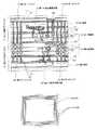
本発明の第1実施の形態に係る半導体装置の構成の第1例を、図1の概略構成断面図およびガードリング部の平面レイアウト図によって説明する。図1(1)に概略構成断面図を示し、(2)にガードリング部の平面レイアウト図を示す。<1. First Embodiment>
[First Example of Configuration of Semiconductor Device]
A first example of the configuration of the semiconductor device according to the first embodiment of the present invention will be described with reference to the schematic configuration cross-sectional view of FIG. FIG. 1A is a schematic cross-sectional view, and FIG. 1B is a plan layout view of the guard ring portion.
図1に示すように、第1半導体デバイス11は、第1基板12に第1半導体集積回路13が形成されている。上記第1半導体集積回路13上には、絶縁膜31とその絶縁膜31中に形成された複数層の配線32からなる第1配線部33を有し、その第1配線部33の側周を囲む耐湿性を有する第1ガードリング14が上記絶縁膜31に形成されている。 As shown in FIG. 1, in the first semiconductor device 11, a first semiconductor integrated circuit 13 is formed on a
一方、第2半導体デバイス21は、第2基板22に第2半導体集積回路23が形成されている。上記第2半導体集積回路23上には、絶縁膜41とその絶縁膜41中に形成された複数層の配線42からなる第2配線部43を有し、その第2配線部43の側周を囲む耐湿性を有する第2ガードリング24が上記絶縁膜41に形成されている。
そして、上記第1半導体デバイス11と上記第2半導体デバイス21が接合された積層されている。On the other hand, in the second semiconductor device 21, the second semiconductor integrated circuit 23 is formed on the second substrate 22. On the second semiconductor integrated circuit 23, there is a
The first semiconductor device 11 and the second semiconductor device 21 are laminated.
上記第1半導体デバイス11と上記第2半導体デバイス21の接合面では上記第1ガードリング14と上記第2ガードリング24とが接合されている。 The
例えば、上記記第1半導体デバイス11と上記第2半導体デバイス21との接合は、接着剤51で成されている。
または、図示していないが、上記第1半導体デバイス11の接合面は第1酸化シリコン膜で形成され、上記第2半導体デバイス21の接合面は第2酸化シリコン膜で形成され、上記第1半導体デバイス11と上記第2半導体デバイス21との接合は、上記第1、第2酸化シリコン膜同士の接合で成されていてもよい。For example, the first semiconductor device 11 and the second semiconductor device 21 are joined with an adhesive 51.
Alternatively, although not shown, the bonding surface of the first semiconductor device 11 is formed of a first silicon oxide film, the bonding surface of the second semiconductor device 21 is formed of a second silicon oxide film, and the first semiconductor device The device 11 and the second semiconductor device 21 may be joined by joining the first and second silicon oxide films.
上記第1ガードリング14と上記第2ガードリング24は、詳細を図示はしていないが、以下のような構成となっている。
例えば、上記第1ガードリング14は、上記第1基板12、上記絶縁膜31等を貫通する貫通溝15の側面に形成された側壁絶縁膜(図示せず)を介して埋め込まれた、アルミニウム、銅、タングステン、チタン、タンタル、窒化チタン、窒化タンタル、ポリシリコン、もしくはそれらの積層構造や、またはアルミニウム、銅、タングステン、チタン、タンタルのいずれか1種以上を主成分とした合金等の耐湿性材料17で形成されている。
したがって、上記第1ガードリング14は、水分や大気成分(主として酸素(O)等の酸化成分)を通すことはない。Although the details of the
For example, the
Therefore, the
また、上記第2ガードリング24は、少なくとも上記絶縁膜41を貫通する貫通溝25の側面に形成された側壁絶縁膜を介して埋め込まれた、アルミニウム、銅、タングステン、チタン、タンタル、窒化チタン、窒化タンタル、ポリシリコン、もしくはそれらの積層構造や、またはアルミニウム、銅、タングステン、チタン、タンタルのいずれか1種以上を主成分とした合金等の耐湿性材料27で形成されている。
したがって、上記第2ガードリング24は、水分や大気成分(主として酸素(O)等の酸化成分)を通すことはない。The
Therefore, the
なお、上記第1ガードリング14、第2ガードリング24は、複数の溝をつなぎ合わせて形成した貫通溝15(25)内に上記耐湿性材料17(27)を埋め込んで形成したものであってもよい。 The
また、上記第1ガードリング14、第2ガードリング24ともに、その幅は、数百nmから数μmとする。例えば、200nm〜4μm程度とする。上記のガードリング材料であれば、200nm以上の厚さがあれば、十分な耐湿性が得られる。また、ガードリングが厚くなれば、接合幅も広くなり、耐湿性の点で有利になるが、4μmを超えるような厚さは必要なく、チップ面積の増大になる。 Further, the width of both the
したがって、上記半導体装置1では、第1半導体デバイス11と第2半導体デバイス21の接合面で、第1ガードリング14と第2ガードリング24とが接合されている。このため、第1半導体デバイス11と第2半導体デバイス21との接合面から侵入した水分や大気成分(主として酸素等の酸化成分)は、第1配線部33や第2配線部43内に侵入することがない。すなわち、接合界面での水分や大気成分の侵入が防止される。このため、第1配線部33の配線32や第2配線部43の配線42が酸化、腐食を受けることがない。
よって、配線の信頼性の向上が図れる。Therefore, in the
Therefore, the reliability of wiring can be improved.
なお、図面では、第1ガードリング14、第2ガードリング24ともに、それぞれ、第1半導体集積回路13、第2半導体集積回路23の側周を三重に囲むように形成されているが、その数は、一重もしくは二重であっても、三重よりも多くてもかまわない。しかし、ガードリング数が多くなると、チップ面積の増大になるので、三重以下に形成されることが好ましい。 In the drawing, both the
また、第1配線部33の配線32と第2配線部43の配線42との電気的接続は、プラグ28によって成されている。このプラグ28は、上記第1、第2ガードリング14、24と同様な構成を有する。 The electrical connection between the
[半導体装置の構成の第2例]
本発明の第1実施の形態に係る半導体装置の構成の第2例を、図2の概略構成断面図によって説明する。[Second Example of Configuration of Semiconductor Device]
A second example of the configuration of the semiconductor device according to the first embodiment of the present invention will be described with reference to the schematic configuration cross-sectional view of FIG.
図2に示すように、第1半導体デバイス11は、第1基板12に第1半導体集積回路13が形成されている。上記第1半導体集積回路13上には、絶縁膜31とその絶縁膜31中に形成された複数層の配線32からなる第1配線部33を有し、その第1配線部33の側周を囲む耐湿性を有する第1ガードリング14が上記絶縁膜31に形成されている。 As shown in FIG. 2, in the first semiconductor device 11, a first semiconductor integrated circuit 13 is formed on a
一方、第2半導体デバイス21は、第2基板22に第2半導体集積回路23が形成されている。上記第2半導体集積回路23上に形成された絶縁膜41とその絶縁膜41中に形成された複数層の配線42からなる第2配線部43を有し、その第2配線部43の側周を囲む耐湿性を有する第2ガードリング24が上記絶縁膜41に形成されている。
そして、上記第1半導体デバイス11と上記第2半導体デバイス21が接合された積層されている。On the other hand, in the second semiconductor device 21, the second semiconductor integrated circuit 23 is formed on the second substrate 22. It has a
The first semiconductor device 11 and the second semiconductor device 21 are laminated.
上記第1半導体デバイス11と上記第2半導体デバイス21の接合面では上記第1ガードリング14と上記第2ガードリング24とが、例えば第2ガードリング24に形成されたバンプ29Aを介して接合されている。もちろん、バンプ29Aは、第1ガードリング14側に形成されていてもよく、第1ガードリング14と第2ガードリング24の両方に形成されていてもよい。
上記バンプ29Aは、例えば、スズ、銅、金、もしくはそれらを主成分とした合金で形成されている。The
The
例えば、上記記第1半導体デバイス11と上記第2半導体デバイス21との接合は、接着剤51で成されている。
または、図示していないが、上記第1半導体デバイス11の接合面は第1酸化シリコン膜で形成され、上記第2半導体デバイス21の接合面は第2酸化シリコン膜で形成され、上記第1半導体デバイス11と上記第2半導体デバイス21との接合は、上記第1、第2酸化シリコン膜同士の接合で成されていてもよい。For example, the first semiconductor device 11 and the second semiconductor device 21 are joined with an adhesive 51.
Alternatively, although not shown, the bonding surface of the first semiconductor device 11 is formed of a first silicon oxide film, the bonding surface of the second semiconductor device 21 is formed of a second silicon oxide film, and the first semiconductor device The device 11 and the second semiconductor device 21 may be joined by joining the first and second silicon oxide films.
上記第1ガードリング14と上記第2ガードリング24は、詳細を図示はしていないが、以下のような構成となっている。
例えば、上記第1ガードリング14は、少なくとも絶縁膜31を貫通する貫通溝15の側面に形成された側壁絶縁膜(図示せず)を介して埋め込まれた、アルミニウム、銅、タングステン、チタン、タンタル、窒化チタン、窒化タンタル、ポリシリコン、もしくはそれらの積層構造や、またはアルミニウム、銅、タングステン、チタン、タンタルのいずれか1種以上を主成分とした合金等の耐湿性材料17で形成されている。
したがって、上記第1ガードリング14は、水分や大気成分(主として酸素(O)等の酸化成分)を通すことはない。Although the details of the
For example, the
Therefore, the
また、上記第2ガードリング24は、少なくとも絶縁膜41を貫通する貫通溝25の側面に形成された絶縁膜を介して埋め込まれた、アルミニウム、銅、タングステン、チタン、タンタル、窒化チタン、窒化タンタル、ポリシリコン、もしくはそれらの積層構造や、またはアルミニウム、銅、タングステン、チタン、タンタルのいずれか1種以上を主成分とした合金等の耐湿性材料27で形成されている。
したがって、上記第2ガードリング24は、水分や大気成分(主として酸素(O)等の酸化成分)を通すことはない。Further, the
Therefore, the
なお、上記第1ガードリング14、第2ガードリング24は、複数の溝をつなぎ合わせて形成した貫通溝15(25)内に上記耐湿性材料17(27)を埋め込んで形成したものであってもよい。 The
また、上記第1ガードリング14、第2ガードリング24ともに、その幅は、数百nmから数μmとする。例えば、200nm〜4μm程度とする。上記のガードリング材料であれば、200nm以上の厚さがあれば、十分な耐湿性が得られる。また、ガードリングが厚くなれば、接合幅も広くなり、耐湿性の点で有利になるが、4μmを超えるような厚さは必要なく、チップ面積の増大になる。 Further, the width of both the
したがって、上記半導体装置2では、第1半導体デバイス11と第2半導体デバイス21の接合面で、第1ガードリング14と第2ガードリング24とがバンプ29を介して接合されているから、第1半導体デバイス11と第2半導体デバイス21との接合面から侵入した水分や大気成分(主として酸素等の酸化成分)は、第1配線部13や第2配線部23内に侵入することがない。すなわち、接合界面での水分や大気成分の侵入が防止される。このため、第1配線部33の配線32や第2配線部43の配線42が酸化、腐食を受けることがない。
よって、配線の信頼性の向上が図れる。Therefore, in the
Therefore, the reliability of wiring can be improved.
なお、図面では、第1ガードリング14、第2ガードリング24ともに、それぞれ、第1半導体集積回路13、第2半導体集積回路23の側周を三重に囲むように形成されているが、その数は、一重もしくは二重であっても、三重よりも多くてもかまわない。しかし、ガードリング数が多くなると、チップ面積の増大になるので、三重以下に形成されることが好ましい。 In the drawing, both the
また、第1配線部33の配線32と第2配線部43の配線42との電気的接続は、バンプ29Bによって成されている。このバンプ29Bは上記バンプ29Aと同様な材料で形成されている。 Further, the electrical connection between the
<2.第2の実施の形態>
[半導体装置の製造方法の第1例]
本発明の第2実施の形態に係る半導体装置の製造方法の第1例を、図3〜図4の製造工程断面図によって説明する。<2. Second Embodiment>
[First Example of Manufacturing Method of Semiconductor Device]
A first example of the method for manufacturing a semiconductor device according to the second embodiment of the present invention will be described with reference to the manufacturing process sectional views of FIGS.
図3(1)に示すように、第1半導体デバイス11は、第1基板12に第1半導体集積回路13が形成されている。上記第1半導体集積回路13上には、絶縁膜31とその絶縁膜31中に形成された複数層の配線32からなる第1配線部33を有している。 As shown in FIG. 3A, in the first semiconductor device 11, a first semiconductor integrated circuit 13 is formed on a
一方、第2半導体デバイス21は、第2基板22に第2半導体集積回路23が形成されている。上記第2半導体集積回路23上には、絶縁膜41とその絶縁膜41中に形成された複数層の配線42からなる第2配線部43を有し、その第2配線部43の側周を囲む耐湿性を有する第2ガードリング24が上記絶縁膜41に形成されている。
上記第1半導体デバイス11と上記第2半導体デバイス21を、例えば接着剤51で貼り合わせる。もしくは、図示はしていないが、上記絶縁膜31の接合面に形成された酸化シリコン膜と、絶縁膜41の接合面に形成された酸化シリコン(SiO2)膜とをプラズマ接合等により貼り合わせる。On the other hand, in the second semiconductor device 21, the second semiconductor integrated circuit 23 is formed on the second substrate 22. On the second semiconductor integrated circuit 23, there is a
The first semiconductor device 11 and the second semiconductor device 21 are bonded together with an adhesive 51, for example. Alternatively, although not shown, the silicon oxide film formed on the bonding surface of the insulating
次に、図3(2)に示すように、例えば第1基板12の裏面側(素子、配線等が形成されていない側)を裏面研削(BGR)や化学的機械研磨(CMP)を使用し、研削もしくは研磨して、第1基板12を薄くする。 Next, as shown in FIG. 3 (2), for example, the back surface side (the side where elements, wirings, etc. are not formed) of the
次に、図4(3)に示すように、ドライエッチング等により、上記第1基板12から上記絶縁膜31を貫通する貫通溝15を形成する。
次に、例えば化学気相成長(CVD)法によって、上記貫通溝15の内面に第1基板12のシリコン(Si)との絶縁を確保する側壁絶縁膜(図示せず)を形成する。
その際、貫通溝15底部に形成された側壁絶縁膜は、異方性の強い、例えば電子ビーム(EB)加工や、異方性エッチングによって除去する。
その後、上記貫通溝15の内部を銅(Cu)、タングステン(W)等の耐湿性材料17で埋め込む。そして、化学的機械研磨(CMP)等で余分な耐湿性材料17を取り除く。
この結果、貫通溝15内の側壁に側壁絶縁膜を介して耐湿性材料17が埋め込まれてなる第1ガードリング14が形成される。
上記耐湿性材料17は、上記第2ガードリング24を構成する耐湿性材料27も同様であり、アルミニウム、銅、タングステン、チタン、タンタル、窒化チタン、窒化タンタル、ポリシリコン、もしくはそれらの積層構造や、またはアルミニウム、銅、タングステン、チタン、タンタルのいずれか1種以上を主成分とした合金等で形成される。Next, as shown in FIG. 4C, through
Next, a sidewall insulating film (not shown) for ensuring insulation from silicon (Si) of the
At this time, the sidewall insulating film formed at the bottom of the through
Thereafter, the inside of the through
As a result, the
The moisture-
また、上記第1ガードリング14を形成するとき、同時に、第1配線部13、第2配線部43の配線32、配線42に接続するプラグ28を形成することはできる。図面では、配線32に接続するプラグ28を示した。 Further, when the
次に、図4(4)に示すように、例えば、第1基板12上に層間絶縁膜61を成膜して第1基板12のシリコン(Si)部分との絶縁を確保する。その後、層間絶縁膜61の所定の位置に配線32に接続されたプラグ28に達する開口部62を形成し、この開口部62を通じて配線32に接続されるパッド電極63を形成する。このパッド電極63は、例えばアルミニウムもしくはアルミニウム合金で形成される。もちろん、上記パッド電極63は、アルミニウム以外の導電性材料で形成されてもよい。 Next, as shown in FIG. 4 (4), for example, an
また、上記貫通溝15、貫通溝25は、その幅が、例えば数百nmから数μmとなるように形成される。例えば、ガードリング材料が200nm〜4μmの幅で埋め込まれるように、側壁絶縁膜の膜厚を考慮して形成される。例えば、側壁絶縁膜の膜厚は、電気的絶縁性は確保されればよいので、例えば酸化シリコン膜の場合、20nm以上とする。また上記のガードリング材料であれば、200nm以上の幅があれば、十分な耐湿性が得られる。また、ガードリングが厚くなれば、接合幅も広くなり、耐湿性の点で有利になるが、4μmを超えるような厚さは必要なく、チップ面積の増大になる。 Further, the through
したがって、上記半導体装置の製造方法では、第1半導体デバイス11と第2半導体デバイス21の接合面で、第1ガードリング14と第2ガードリング24とが接合されることから、第1半導体デバイス11と第2半導体デバイス21との接合面から侵入した水分や大気成分(主として酸素等の酸化成分)は、第1配線部33や第2配線部43内に侵入することがない。このため、第1配線部33の配線32や第2配線部43の配線42が酸化、腐食を受けることがない。
よって、配線の信頼性の向上が図れる。Therefore, in the method for manufacturing a semiconductor device, the
Therefore, the reliability of wiring can be improved.
なお、図面では、第1ガードリング14、第2ガードリング24ともに、それぞれ、第1半導体集積回路13、第2半導体集積回路23の側周を三重に囲むように形成されているが、その数は、一重もしくは二重であっても、三重よりも多くてもかまわない。しかし、ガードリング数が多くなると、チップ面積の増大になるので、三重以下に形成されることが好ましい。 In the drawing, both the
[半導体装置の製造方法の第2例]
本発明の第2実施の形態に係る半導体装置の製造方法の第2例を、図5〜図6の製造工程断面図によって説明する。[Second Example of Manufacturing Method of Semiconductor Device]
A second example of the method of manufacturing a semiconductor device according to the second embodiment of the present invention will be described with reference to the manufacturing process sectional views of FIGS.
図5(1)に示すように、第1半導体デバイス11は、第1基板12に第1半導体集積回路13が形成されている。上記第1半導体集積回路13上には、絶縁膜31とその絶縁膜31中に形成された複数層の配線32からなる第1配線部33を有し、その第1配線部33の側周を囲む耐湿性を有する第1ガードリング14が上記絶縁膜31に形成されている。
上記第1ガードリング14の接合部には、接合用パッド14Pが形成されていることが好ましい。As shown in FIG. 5A, in the first semiconductor device 11, the first semiconductor integrated circuit 13 is formed on the
It is preferable that a
一方、第2半導体デバイス21は、第2基板22に第2半導体集積回路23が形成されている。上記第2半導体集積回路23上には、絶縁膜41とその絶縁膜41中に形成された複数層の配線42からなる第2配線部43を有し、その第2配線部43の側周を囲む耐湿性を有する第2ガードリング24が上記絶縁膜41に形成されている。
上記第2ガードリング24の接合部には、接合用パッド24P(上記バンプ29Aに対応)が形成されていることが好ましい。On the other hand, in the second semiconductor device 21, the second semiconductor integrated circuit 23 is formed on the second substrate 22. On the second semiconductor integrated circuit 23, there is a
It is preferable that a
そして、上記第1半導体デバイス11と上記第2半導体デバイス21を、例えば接着剤51で貼り合わせる。もしくは、図示はしていないが、上記絶縁膜31の接合面に形成された酸化シリコン膜と、絶縁膜41の接合面に形成された酸化シリコン(SiO2)膜とをプラズマ接合等により貼り合わせる。Then, the first semiconductor device 11 and the second semiconductor device 21 are bonded together with an adhesive 51, for example. Alternatively, although not shown, the silicon oxide film formed on the bonding surface of the insulating
このとき、上記第1ガードリング14の接合用パッド14Pと上記第2ガードリング24の接合用パッド24Pとが接合される。なお、上記接着剤51を用いて説明する場合、上記接着剤51が接合用パッド14P表面、接合用パッド24P表面に被着されないようにしている。例えば、接合用パッド14P表面および接合用パッド24P表面以外の領域に接着剤51を形成して貼り合わせてもよい。その際、接着剤51の被着は、第1半導体デバイス11側でも第2半導体デバイス21側でも、その両方でもよい。または例えば、接合用パッド14P表面と接合用パッド24P表面を接合した後、隙間に接着剤51を充填してもよい。 At this time, the bonding pad 14P of the
次に、図5(2)に示すように、例えば第1基板12の裏面側(素子、配線等が形成されていない側)を裏面研削(BGR)や化学的機械研磨(CMP)を使用し、研削もしくは研磨して、第1基板12を薄くする。 Next, as shown in FIG. 5 (2), for example, the back surface side (the side where elements, wirings, etc. are not formed) of the
次に、図6(3)に示すように、ドライエッチング等により、上記第1基板12から上記絶縁膜31を貫通して第1配線部33の配線32の一部に達する貫通孔35を形成する。
次に、例えば化学気相成長(CVD)法によって、上記貫通孔35の内面に第1基板12のシリコン(Si)との絶縁を確保する側壁絶縁膜(図示せず)を形成する。
その際、貫通孔35底部に形成された側壁絶縁膜は、異方性の強い、例えば電子ビーム(EB)加工や、異方性エッチングによって除去する。
その後、上記貫通孔35の内部を銅(Cu)、タングステン(W)等の導電性材料37で埋め込む。そして、化学的機械研磨(CMP)等で余分な導電性材料37を取り除く。
この結果、貫通孔35内の側壁に側壁絶縁膜を介して導電性材料37が埋め込まれてなるプラグ38が形成される。
上記導電性材料37は、上記耐湿性材料17と同様であり、アルミニウム、銅、タングステン、チタン、タンタル、窒化チタン、窒化タンタル、ポリシリコン、もしくはそれらの積層構造や、またはアルミニウム、銅、タングステン、チタン、タンタルのいずれか1種以上を主成分とした合金等で形成される。Next, as shown in FIG. 6 (3), through-
Next, a sidewall insulating film (not shown) for ensuring insulation from silicon (Si) of the
At this time, the sidewall insulating film formed at the bottom of the through
Thereafter, the inside of the through
As a result, a
The
次に、図6(4)に示すように、例えば、第1基板12上に層間絶縁膜61を成膜して第1基板12のシリコン(Si)部分との絶縁を確保する。その後、層間絶縁膜61の所定の位置に配線32に接続されたプラグ38に達する開口部62を形成し、この開口部62を通じて配線32に接続されるパッド電極63を形成する。このパッド電極63は、例えばアルミニウムもしくはアルミニウム合金で形成される。もちろん、上記パッド電極63は、アルミニウム以外の導電性材料で形成されてもよい。 Next, as shown in FIG. 6 (4), for example, an
また、上記貫通溝15、貫通溝25は、その幅が、例えば数百nmから数μmとなるように形成される。例えば、ガードリング材料が200nm〜4μmの幅で埋め込まれるように、側壁絶縁膜の膜厚を考慮して形成される。例えば、側壁絶縁膜の膜厚は、電気的絶縁性は確保されればよいので、例えば酸化シリコン膜の場合、20nm以上とする。また上記のガードリング材料であれば、200nm以上の幅があれば、十分な耐湿性が得られる。また、ガードリングが厚くなれば、接合幅も広くなり、耐湿性の点で有利になるが、4μmを超えるような厚さは必要なく、チップ面積の増大になる。 Further, the through
したがって、上記半導体装置の製造方法(第2例)では、第1半導体デバイス11と第2半導体デバイス21の接合面で、第1ガードリング14と第2ガードリング24とが接合されることから、第1半導体デバイス11と第2半導体デバイス21との接合面から侵入した水分や大気成分(主として酸素等の酸化成分)は、第1配線部33や第2配線部43内に侵入することがない。このため、第1配線部33の配線32や第2配線部43の配線42が酸化、腐食を受けることがない。
よって、配線の信頼性の向上が図れる。Therefore, in the semiconductor device manufacturing method (second example), the
Therefore, the reliability of wiring can be improved.
なお、図面では、第1ガードリング14、第2ガードリング24ともに、それぞれ、第1半導体集積回路13、第2半導体集積回路23の側周を三重に囲むように形成されているが、その数は、一重もしくは二重であっても、三重よりも多くてもかまわない。しかし、ガードリング数が多くなると、チップ面積の増大になるので、三重以下に形成されることが好ましい。 In the drawing, both the
また、上記各製造方法において、貫通溝15,25、貫通孔35等を形成するには、例えば、ドライエッチングを用いる。 In each of the above manufacturing methods, for example, dry etching is used to form the through
シリコン(Si)部分のドライエッチングでは、例えば、エッチングガスに、サルファーヘキサフルオライド(SF6)と、酸素(O2)を用いる。そのエッチング雰囲気の圧力を24Pa、RFパワーを700Wに設定される。エッチングガス流量は、サルファーヘキサフルオライド(SF6)を100cm3/min、酸素(O2)を80cm3/minに設定される。さらに、基板温度を、トップ側を40℃、サイド部分を40℃、底部を30℃に設定される。上記条件は一例であって、上記条件に限定されない。In dry etching of a silicon (Si) portion, for example, sulfur hexafluoride (SF6 ) and oxygen (O2 ) are used as an etching gas. The pressure of the etching atmosphere is set to 24 Pa and the RF power is set to 700 W. Etching gas flow rate is set sulfur hexafluoride and(SF 6) 100cm 3 / min , the oxygen (O2) to 80 cm3 / min. Further, the substrate temperature is set to 40 ° C. on the top side, 40 ° C. on the side portion, and 30 ° C. on the bottom portion. The above condition is an example and is not limited to the above condition.
上記絶縁膜31、絶縁膜41が酸化シリコン(SiO2)である場合のエッチングでは、例えば、エッチングガスにオクタフルオロシクロブタン(C4F8)、酸素(O2)、アルゴン(Ar)を用いる。そのエッチング雰囲気の圧力を5.3Pa、RFパワーを1500W、バイアスパワーを700Wに設定する。また、エッチングガス流量は、オクタフルオロシクロブタン(C4F8)を16cm3/min、酸素(O2)を10cm3/min、アルゴン(Ar)を900cm3/minに設定する。さらに基板温度を、トップ側を60℃、サイド部分を60℃、底部を20℃に設定する。上記条件は一例であって、上記条件に限定されない。In the etching in the case where the insulating
上記絶縁膜31、絶縁膜41がベンゾシクロブテン(BCB)である場合の上記絶縁膜31、絶縁膜41のドライエッチングでは、エッチングガスに、オクタフルオロシクロブタン(C4F8)、酸素(O2)、窒素(N2)を用いる。また、エッチング雰囲気の圧力を13.3Pa、RFパワーを1500W、バイアスパワーを700Wに設定される。また、エッチングガス流量は、オクタフルオロシクロブタン(C4F8)を10cm3/min、酸素(O2)を50cm3/min、窒素(N2)を500cm3/minに設定する。さらにエッチング雰囲気の温度を例えば23℃(室温)に設定する。上記条件は一例であって、上記条件に限定されない。In the dry etching of the insulating
また、プラズマ処理による第1半導体デバイス11の酸化シリコン膜と第2半導体デバイス21の酸化シリコン膜との接合に用いるプラズマ接合条件の一例として、プラズマパワーを200W、プラズマ接合雰囲気の圧力を0.67kPa、プロセスガスに窒素(N2)を用い、基板温度を23℃(室温)とした。上記条件は一例であって、上記条件に限定されない。As an example of plasma bonding conditions used for bonding the silicon oxide film of the first semiconductor device 11 and the silicon oxide film of the second semiconductor device 21 by plasma processing, the plasma power is 200 W and the pressure of the plasma bonding atmosphere is 0.67 kPa. Nitrogen (N2 ) was used as the process gas, and the substrate temperature was 23 ° C. (room temperature). The above condition is an example and is not limited to the above condition.
また、接合時に行うアニールの条件としては、アニール温度を400℃、アニール雰囲気の圧力を周囲圧力(例えば、大気圧)、プロセスガスに窒素(N2)を用い、アニール時間を1時間とした。また、ロード、アンロードにおける温度を400℃に設定した。上記条件は一例であって、上記条件に限定されない。
なお、接合に係る圧着は、プラズマ処理後に重ね合わせてアニール処理するだけで貼り合わせが可能である。The annealing conditions for the bonding were as follows: annealing temperature was 400 ° C., annealing atmosphere pressure was ambient pressure (eg, atmospheric pressure), process gas was nitrogen (N2 ), and annealing time was 1 hour. The temperature during loading and unloading was set to 400 ° C. The above condition is an example and is not limited to the above condition.
Note that the bonding for bonding can be performed by simply superposing and annealing after the plasma treatment.
11…第1半導体デバイス、12…第1基板、13…第1半導体集積回路、14…第1ガードリング、21…第1半導体デバイス、22…第2基板、23…第2半導体集積回路、24…第2ガードリング、31…絶縁膜、32…配線、33…第1配線部、41…絶縁膜、42…配線、43…第2配線部 DESCRIPTION OF SYMBOLS 11 ... 1st semiconductor device, 12 ... 1st board | substrate, 13 ... 1st semiconductor integrated circuit, 14 ... 1st guard ring, 21 ... 1st semiconductor device, 22 ... 2nd board | substrate, 23 ... 2nd semiconductor integrated circuit, 24 ... second guard ring, 31 ... insulating film, 32 ... wiring, 33 ... first wiring portion, 41 ... insulating film, 42 ... wiring, 43 ... second wiring portion
Claims (13)
Translated fromJapanese第2基板に第2半導体集積回路が形成され、その第2半導体集積回路上に形成された絶縁膜とその絶縁膜中に形成された複数層の配線からなる第2配線部の側周を囲む耐湿性を有する第2ガードリングを備えた第2半導体デバイスが、前記第1配線部と前記第2配線部とを対向させて積層されていて、
前記第1半導体デバイスと前記第2半導体デバイスの接合面で前記第1ガードリングと前記第2ガードリングとが接合されている
半導体装置。A first semiconductor integrated circuit is formed on a first substrate, and surrounds a side periphery of a first wiring portion including an insulating film formed on the first semiconductor integrated circuit and a plurality of layers of wiring formed in the insulating film. A first semiconductor device comprising a first guard ring having moisture resistance;
A second semiconductor integrated circuit is formed on the second substrate, and surrounds a side periphery of a second wiring portion made up of an insulating film formed on the second semiconductor integrated circuit and a plurality of layers of wiring formed in the insulating film. A second semiconductor device comprising a second guard ring having moisture resistance is laminated with the first wiring portion and the second wiring portion facing each other;
A semiconductor device in which the first guard ring and the second guard ring are joined at a joint surface between the first semiconductor device and the second semiconductor device.
請求項1記載の半導体装置。The semiconductor device according to claim 1, wherein the first semiconductor device and the second semiconductor device are joined with an adhesive.
前記第2半導体デバイスの接合面は第2酸化シリコン膜で形成され、
前記第1半導体デバイスと前記第2半導体デバイスとの接合は、前記第1、第2酸化シリコン膜同士の接合で成されている
請求項1記載の半導体装置。A bonding surface of the first semiconductor device is formed of a first silicon oxide film;
A bonding surface of the second semiconductor device is formed of a second silicon oxide film;
The semiconductor device according to claim 1, wherein a junction between the first semiconductor device and the second semiconductor device is formed by a junction between the first and second silicon oxide films.
前記第2半導体デバイスの接合面における前記第2半導体集積回路の第2配線が接合されていて、
前記第1配線と前記第2配線との接合は、それぞれの配線に形成されたバンプを介して接合されていて、
前記第1ガードリングと前記第2ガードリングとの接合は、それぞれのガードリングに形成されたバンプを介して接合されている
請求項1,2または3記載の半導体装置。A first wiring of the first semiconductor integrated circuit at a bonding surface of the first semiconductor device;
The second wiring of the second semiconductor integrated circuit on the bonding surface of the second semiconductor device is bonded;
The bonding between the first wiring and the second wiring is bonded via a bump formed on each wiring,
The semiconductor device according to claim 1, wherein the first guard ring and the second guard ring are joined via bumps formed on the respective guard rings.
請求項1ないし請求項4のうちの1項に記載の半導体装置。The first guard ring and the second guard ring are made of aluminum, copper, tungsten, titanium, tantalum, embedded through an insulating film in a through hole formed in each of the first substrate and the second substrate. 5. The titanium nitride, tantalum nitride, polysilicon, or a laminated structure thereof, or an alloy mainly containing at least one of aluminum, copper, tungsten, titanium, and tantalum. 2. A semiconductor device according to item 1.
請求項4記載の半導体装置。The semiconductor device according to claim 4, wherein the bump is made of tin, copper, gold, or an alloy containing these as a main component.
第2基板に第2半導体集積回路が形成され、その第2半導体集積回路上に形成された絶縁膜とその絶縁膜中に形成された複数層の配線からなる第2配線部を備えた第2半導体デバイスを、前記第1配線部と前記第2配線部とを対向させて積層する工程と、
前記第1基板に前記第1配線部の側周を囲む耐湿性を有する第1ガードリングを前記第2ガードリングに接合させて形成する工程を備えた
半導体装置の製造方法。A first semiconductor integrated circuit is formed on a first substrate, and includes a first wiring portion including an insulating film formed on the first semiconductor integrated circuit and a plurality of wiring layers formed in the insulating film. A semiconductor device;
A second semiconductor integrated circuit is formed on the second substrate, and includes a second wiring portion including an insulating film formed on the second semiconductor integrated circuit and a plurality of layers of wiring formed in the insulating film. Laminating a semiconductor device with the first wiring portion and the second wiring portion facing each other;
A method for manufacturing a semiconductor device, comprising: forming a first guard ring having moisture resistance surrounding the side periphery of the first wiring portion on the first substrate by bonding the first guard ring to the second guard ring.
第2基板に第2半導体集積回路が形成され、その第2半導体集積回路上に形成された絶縁膜とその絶縁膜中に形成された複数層の配線からなる第2配線部を備えた第2半導体デバイスを、前記第1配線部と前記第2配線部とを対向させて積層する工程と、
前記第2基板に前記第2半導体集積回路の側周を囲む耐湿性を有する第2ガードリングを前記第1ガードリングに接合させて形成する工程を備えた
半導体装置の製造方法。A first semiconductor integrated circuit is formed on a first substrate, and a moisture resistance is provided on a side periphery of a first wiring portion including an insulating film formed on the first semiconductor integrated circuit and a plurality of layers of wiring formed in the insulating film. A first semiconductor device comprising a first guard ring having a property;
A second semiconductor integrated circuit is formed on the second substrate, and includes a second wiring portion including an insulating film formed on the second semiconductor integrated circuit and a plurality of layers of wiring formed in the insulating film. Laminating a semiconductor device with the first wiring portion and the second wiring portion facing each other;
A method of manufacturing a semiconductor device, comprising: forming a second guard ring having moisture resistance surrounding a side periphery of the second semiconductor integrated circuit on the second substrate by bonding the second guard ring to the first guard ring.
請求項7または8記載の半導体装置の製造方法。The method for manufacturing a semiconductor device according to claim 7, wherein the first semiconductor device and the second semiconductor device are joined with an adhesive.
前記第2半導体デバイスの接合面に第2酸化シリコン膜が形成され、
前記第1半導体デバイスと前記第2半導体デバイスとの接合は、前記第1、第2酸化シリコン膜同士の接合で成される
請求項7または8記載の半導体装置の製造方法。A first silicon oxide film is formed on the bonding surface of the first semiconductor device;
A second silicon oxide film is formed on the bonding surface of the second semiconductor device;
The method for manufacturing a semiconductor device according to claim 7, wherein the first semiconductor device and the second semiconductor device are joined by joining the first and second silicon oxide films.
同時に、前記第1ガードリングと前記第2ガードリングとの接合は、それぞれまたは一方のガードリングに形成されたバンプを介して接合する
請求項8、9または10に記載の半導体装置の製造方法。The first wiring of the first semiconductor integrated circuit on the bonding surface of the first semiconductor device and the bonding of the second wiring of the second semiconductor integrated circuit on the bonding surface of the second semiconductor device are connected in advance to each wiring. Join through the formed bumps,
11. The method of manufacturing a semiconductor device according to claim 8, wherein the first guard ring and the second guard ring are joined together via bumps formed on each or one of the guard rings.
請求項7ないし請求項11のうちの1項に記載の半導体装置の製造方法。The first guard ring and the second guard ring are made of aluminum, copper, tungsten, titanium, tantalum, titanium nitride embedded in through holes formed in the first substrate and the second substrate, respectively, through an insulating film. The tantalum nitride, polysilicon, or a laminated structure thereof, or an alloy mainly containing at least one of aluminum, copper, tungsten, titanium, and tantalum. 2. A method for manufacturing a semiconductor device according to item 1.
請求項11記載の半導体装置の製造方法。The method for manufacturing a semiconductor device according to claim 11, wherein the bumps are formed of tin, copper, gold, or an alloy containing them as a main component.
Priority Applications (1)
| Application Number | Priority Date | Filing Date | Title |
|---|---|---|---|
| JP2009200117AJP2011054637A (en) | 2009-08-31 | 2009-08-31 | Semiconductor device and method of manufacturing the same |
Applications Claiming Priority (1)
| Application Number | Priority Date | Filing Date | Title |
|---|---|---|---|
| JP2009200117AJP2011054637A (en) | 2009-08-31 | 2009-08-31 | Semiconductor device and method of manufacturing the same |
Publications (1)
| Publication Number | Publication Date |
|---|---|
| JP2011054637Atrue JP2011054637A (en) | 2011-03-17 |
Family
ID=43943385
Family Applications (1)
| Application Number | Title | Priority Date | Filing Date |
|---|---|---|---|
| JP2009200117APendingJP2011054637A (en) | 2009-08-31 | 2009-08-31 | Semiconductor device and method of manufacturing the same |
Country Status (1)
| Country | Link |
|---|---|
| JP (1) | JP2011054637A (en) |
Cited By (34)
| Publication number | Priority date | Publication date | Assignee | Title |
|---|---|---|---|---|
| JP2012204444A (en)* | 2011-03-24 | 2012-10-22 | Sony Corp | Semiconductor device and manufacturing method of the same |
| JP2012204443A (en)* | 2011-03-24 | 2012-10-22 | Sony Corp | Semiconductor device and manufacturing method of the same |
| WO2012161044A1 (en)* | 2011-05-24 | 2012-11-29 | ソニー株式会社 | Semiconductor device |
| JP2012256736A (en)* | 2011-06-09 | 2012-12-27 | Sony Corp | Semiconductor device |
| JP2013033900A (en)* | 2011-07-05 | 2013-02-14 | Sony Corp | Semiconductor device, electronic apparatus, method of fabricating semiconductor device |
| WO2015019836A1 (en) | 2013-08-05 | 2015-02-12 | ソニー株式会社 | Imaging device and electronic device |
| WO2015019837A1 (en) | 2013-08-05 | 2015-02-12 | ソニー株式会社 | Conversion device, imaging device, electronic device, and conversion method |
| US8963319B2 (en) | 2011-06-20 | 2015-02-24 | Kabushiki Kaisha Toshiba | Semiconductor chip with through hole vias |
| WO2015040798A1 (en)* | 2013-09-20 | 2015-03-26 | パナソニックIpマネジメント株式会社 | Semiconductor device and manufacturing method therefor |
| JP2015162640A (en)* | 2014-02-28 | 2015-09-07 | ルネサスエレクトロニクス株式会社 | Semiconductor device and manufacturing method thereof |
| WO2016117124A1 (en)* | 2015-01-23 | 2016-07-28 | オリンパス株式会社 | Image-capturing device and endoscope |
| US9443802B2 (en) | 2011-07-05 | 2016-09-13 | Sony Corporation | Semiconductor device, fabrication method for a semiconductor device and electronic apparatus |
| WO2016185883A1 (en)* | 2015-05-18 | 2016-11-24 | ソニー株式会社 | Semiconductor device and imaging device |
| WO2017002200A1 (en)* | 2015-06-30 | 2017-01-05 | オリンパス株式会社 | Semiconductor device |
| JP2017120939A (en)* | 2010-06-30 | 2017-07-06 | キヤノン株式会社 | Solid-state imaging device |
| JP2017120913A (en)* | 2015-12-29 | 2017-07-06 | 台湾積體電路製造股▲ふん▼有限公司Taiwan Semiconductor Manufacturing Company,Ltd. | Stack ring structure of stack integrated circuit |
| KR20170139342A (en)* | 2016-06-09 | 2017-12-19 | 삼성전자주식회사 | wafer-to-wafer bonding structure |
| JP2018022924A (en)* | 2017-10-25 | 2018-02-08 | キヤノン株式会社 | Solid state image pickup device and method of manufacturing the same |
| US9972650B2 (en) | 2010-06-30 | 2018-05-15 | Canon Kabushiki Kaisha | Solid-state imaging apparatus and method for manufacturing the solid-state imaging apparatus having sealing portion disposed in bonded members |
| US10229948B2 (en) | 2012-09-28 | 2019-03-12 | Canon Kabushiki Kaisha | Semiconductor apparatus |
| CN110534507A (en)* | 2018-05-25 | 2019-12-03 | 台湾积体电路制造股份有限公司 | Through-silicon via design, three dimensional integrated circuits and its manufacturing method |
| JP2019212729A (en)* | 2018-06-04 | 2019-12-12 | ルネサスエレクトロニクス株式会社 | Semiconductor device and method for manufacturing semiconductor device |
| WO2020175712A2 (en) | 2019-02-28 | 2020-09-03 | Sony Semiconductor Solutions Corporation | Image sensor |
| CN113437077A (en)* | 2020-03-23 | 2021-09-24 | 铠侠股份有限公司 | Semiconductor device with a plurality of semiconductor chips |
| CN113785394A (en)* | 2019-06-12 | 2021-12-10 | 伊文萨思粘合技术公司 | Sealed bonding structure and method of forming the same |
| CN113892170A (en)* | 2021-08-31 | 2022-01-04 | 长江存储科技有限责任公司 | Semiconductor device with sealing ring |
| JP2022509249A (en)* | 2019-01-30 | 2022-01-20 | 長江存儲科技有限責任公司 | Semiconductor devices, junction structures and methods for forming semiconductor devices |
| JP2022130097A (en)* | 2021-02-25 | 2022-09-06 | キオクシア株式会社 | Semiconductor device and its manufacturing method |
| US11462496B2 (en) | 2018-03-07 | 2022-10-04 | Kioxia Corporation | Semiconductor device |
| WO2024042996A1 (en)* | 2022-08-26 | 2024-02-29 | ソニーセミコンダクタソリューションズ株式会社 | Laminated substrate and semiconductor device |
| US12009325B2 (en) | 2020-11-04 | 2024-06-11 | Samsung Electronics Co., Ltd. | Semiconductor device and electronic system including the same |
| WO2024190271A1 (en)* | 2023-03-13 | 2024-09-19 | 富士フイルム株式会社 | Semiconductor device |
| WO2025047553A1 (en)* | 2023-08-30 | 2025-03-06 | ソニーセミコンダクタソリューションズ株式会社 | Semiconductor device, electronic apparatus, and method for manufacturing semiconductor device |
| US12381119B2 (en) | 2017-03-21 | 2025-08-05 | Adeia Semiconductor Bonding Technologies Inc. | Seal for microelectronic assembly |
- 2009
- 2009-08-31JPJP2009200117Apatent/JP2011054637A/enactivePending
Cited By (87)
| Publication number | Priority date | Publication date | Assignee | Title |
|---|---|---|---|---|
| US12074181B2 (en) | 2010-06-30 | 2024-08-27 | Canon Kabushiki Kaisha | Solid-state imaging apparatus and method for manufacturing the solid-state imaging apparatus having sealing portion disposed in bonded members |
| JP2020191467A (en)* | 2010-06-30 | 2020-11-26 | キヤノン株式会社 | Solid state imaging device |
| JP2018160674A (en)* | 2010-06-30 | 2018-10-11 | キヤノン株式会社 | Solid state imaging device |
| US9972650B2 (en) | 2010-06-30 | 2018-05-15 | Canon Kabushiki Kaisha | Solid-state imaging apparatus and method for manufacturing the solid-state imaging apparatus having sealing portion disposed in bonded members |
| US10847558B2 (en) | 2010-06-30 | 2020-11-24 | Canon Kabushiki Kaisha | Solid-state imaging apparatus and method for manufacturing the solid-state imaging apparatus having sealing portion disposed in bonded members |
| JP2022132369A (en)* | 2010-06-30 | 2022-09-08 | キヤノン株式会社 | Solid state imaging device |
| JP7309670B2 (en) | 2010-06-30 | 2023-07-18 | キヤノン株式会社 | Solid-state imaging device |
| JP2017120939A (en)* | 2010-06-30 | 2017-07-06 | キヤノン株式会社 | Solid-state imaging device |
| JP2012204443A (en)* | 2011-03-24 | 2012-10-22 | Sony Corp | Semiconductor device and manufacturing method of the same |
| JP2012204444A (en)* | 2011-03-24 | 2012-10-22 | Sony Corp | Semiconductor device and manufacturing method of the same |
| KR20220030312A (en)* | 2011-05-24 | 2022-03-10 | 소니그룹주식회사 | Semiconductor device |
| TWI578484B (en)* | 2011-05-24 | 2017-04-11 | Sony Corp | Semiconductor device |
| WO2012161044A1 (en)* | 2011-05-24 | 2012-11-29 | ソニー株式会社 | Semiconductor device |
| TWI728248B (en)* | 2011-05-24 | 2021-05-21 | 日商新力股份有限公司 | Imaging device |
| EP3534399A1 (en)* | 2011-05-24 | 2019-09-04 | Sony Corporation | Semiconductor device |
| CN105938825A (en)* | 2011-05-24 | 2016-09-14 | 索尼公司 | Semiconductor image receiving device |
| TWI667763B (en)* | 2011-05-24 | 2019-08-01 | 日商新力股份有限公司 | A semiconductor image reception device |
| US11923279B2 (en) | 2011-05-24 | 2024-03-05 | Sony Group Corporation | Semiconductor device |
| TWI746146B (en)* | 2011-05-24 | 2021-11-11 | 日商新力股份有限公司 | Semiconductor device |
| CN103503122A (en)* | 2011-05-24 | 2014-01-08 | 索尼公司 | Semiconductor device |
| KR20140022039A (en)* | 2011-05-24 | 2014-02-21 | 소니 주식회사 | Semiconductor device |
| KR102574526B1 (en) | 2011-05-24 | 2023-09-07 | 소니그룹주식회사 | Semiconductor device |
| US10236238B2 (en) | 2011-05-24 | 2019-03-19 | Sony Corporation | Semiconductor device |
| US9799587B2 (en) | 2011-05-24 | 2017-10-24 | Sony Corporation | Semiconductor device |
| KR101952976B1 (en)* | 2011-05-24 | 2019-02-27 | 소니 주식회사 | Semiconductor device |
| US11626356B2 (en) | 2011-05-24 | 2023-04-11 | Sony Group Corporation | Semiconductor device |
| US11587857B2 (en) | 2011-05-24 | 2023-02-21 | Sony Corporation | Semiconductor device |
| EP2717300A4 (en)* | 2011-05-24 | 2015-04-22 | Sony Corp | SEMICONDUCTOR COMPONENT |
| JP2012256736A (en)* | 2011-06-09 | 2012-12-27 | Sony Corp | Semiconductor device |
| US8963319B2 (en) | 2011-06-20 | 2015-02-24 | Kabushiki Kaisha Toshiba | Semiconductor chip with through hole vias |
| US11569123B2 (en) | 2011-07-05 | 2023-01-31 | Sony Corporation | Semiconductor device, fabrication method for a semiconductor device and electronic apparatus |
| JP2013033900A (en)* | 2011-07-05 | 2013-02-14 | Sony Corp | Semiconductor device, electronic apparatus, method of fabricating semiconductor device |
| US9443802B2 (en) | 2011-07-05 | 2016-09-13 | Sony Corporation | Semiconductor device, fabrication method for a semiconductor device and electronic apparatus |
| US10229948B2 (en) | 2012-09-28 | 2019-03-12 | Canon Kabushiki Kaisha | Semiconductor apparatus |
| WO2015019836A1 (en) | 2013-08-05 | 2015-02-12 | ソニー株式会社 | Imaging device and electronic device |
| WO2015019837A1 (en) | 2013-08-05 | 2015-02-12 | ソニー株式会社 | Conversion device, imaging device, electronic device, and conversion method |
| US10068876B2 (en) | 2013-09-20 | 2018-09-04 | Panasonic Intellectual Property Management Co., Ltd. | Semiconductor device and manufacturing method therefor |
| JPWO2015040798A1 (en)* | 2013-09-20 | 2017-03-02 | パナソニックIpマネジメント株式会社 | Semiconductor device and manufacturing method thereof |
| WO2015040798A1 (en)* | 2013-09-20 | 2015-03-26 | パナソニックIpマネジメント株式会社 | Semiconductor device and manufacturing method therefor |
| JP2015162640A (en)* | 2014-02-28 | 2015-09-07 | ルネサスエレクトロニクス株式会社 | Semiconductor device and manufacturing method thereof |
| JPWO2016117124A1 (en)* | 2015-01-23 | 2017-11-02 | オリンパス株式会社 | Imaging apparatus and endoscope |
| WO2016117124A1 (en)* | 2015-01-23 | 2016-07-28 | オリンパス株式会社 | Image-capturing device and endoscope |
| US10622398B2 (en) | 2015-01-23 | 2020-04-14 | Olympus Corporation | Image pickup apparatus and endoscope comprising a guard ring formed along an outer edge on a wire layer and a through-hole with an electrode pad having outer periphery portion in contact with a silicon layer over a whole periphery |
| JP2022173467A (en)* | 2015-05-18 | 2022-11-18 | ソニーグループ株式会社 | Semiconductor device and imaging device |
| US11069735B2 (en) | 2015-05-18 | 2021-07-20 | Sony Corporation | Semiconductor device and imaging device |
| CN111883501A (en)* | 2015-05-18 | 2020-11-03 | 索尼公司 | Semiconductor device and imaging device |
| US10720462B2 (en)* | 2015-05-18 | 2020-07-21 | Sony Corporation | Semiconductor device and imaging device |
| JP7151748B2 (en) | 2015-05-18 | 2022-10-12 | ソニーグループ株式会社 | Semiconductor device and imaging device |
| JP2020198459A (en)* | 2015-05-18 | 2020-12-10 | ソニー株式会社 | Semiconductor device and imaging device |
| JP7424445B2 (en) | 2015-05-18 | 2024-01-30 | ソニーグループ株式会社 | Semiconductor devices and imaging devices |
| JPWO2016185883A1 (en)* | 2015-05-18 | 2018-03-08 | ソニー株式会社 | Semiconductor device and imaging device |
| CN107615481A (en)* | 2015-05-18 | 2018-01-19 | 索尼公司 | Semiconductor device and imaging device |
| WO2016185883A1 (en)* | 2015-05-18 | 2016-11-24 | ソニー株式会社 | Semiconductor device and imaging device |
| CN111883501B (en)* | 2015-05-18 | 2024-10-18 | 索尼公司 | Light detection device and imaging device |
| US10355039B2 (en) | 2015-05-18 | 2019-07-16 | Sony Corporation | Semiconductor device and imaging device |
| US20180061779A1 (en)* | 2015-06-30 | 2018-03-01 | Olympus Corporation | Semiconductor device |
| JPWO2017002200A1 (en)* | 2015-06-30 | 2018-04-19 | オリンパス株式会社 | Semiconductor device |
| WO2017002200A1 (en)* | 2015-06-30 | 2017-01-05 | オリンパス株式会社 | Semiconductor device |
| JP2017120913A (en)* | 2015-12-29 | 2017-07-06 | 台湾積體電路製造股▲ふん▼有限公司Taiwan Semiconductor Manufacturing Company,Ltd. | Stack ring structure of stack integrated circuit |
| CN107026151A (en)* | 2015-12-29 | 2017-08-08 | 台湾积体电路制造股份有限公司 | Three-dimensional integrated circuit chip and forming method thereof |
| KR102505856B1 (en)* | 2016-06-09 | 2023-03-03 | 삼성전자 주식회사 | wafer-to-wafer bonding structure |
| KR20170139342A (en)* | 2016-06-09 | 2017-12-19 | 삼성전자주식회사 | wafer-to-wafer bonding structure |
| US12381119B2 (en) | 2017-03-21 | 2025-08-05 | Adeia Semiconductor Bonding Technologies Inc. | Seal for microelectronic assembly |
| JP2018022924A (en)* | 2017-10-25 | 2018-02-08 | キヤノン株式会社 | Solid state image pickup device and method of manufacturing the same |
| US11462496B2 (en) | 2018-03-07 | 2022-10-04 | Kioxia Corporation | Semiconductor device |
| US12218088B2 (en) | 2018-03-07 | 2025-02-04 | Kioxia Corporation | Semiconductor device |
| US11063038B2 (en) | 2018-05-25 | 2021-07-13 | Taiwan Semiconductor Manufacturing Company, Ltd. | Through silicon via design for stacking integrated circuits |
| CN110534507A (en)* | 2018-05-25 | 2019-12-03 | 台湾积体电路制造股份有限公司 | Through-silicon via design, three dimensional integrated circuits and its manufacturing method |
| US10964692B2 (en) | 2018-05-25 | 2021-03-30 | Taiwan Semiconductor Manufacturing Co., Ltd. | Through silicon via design for stacking integrated circuits |
| US11646308B2 (en) | 2018-05-25 | 2023-05-09 | Taiwan Semiconductor Manufacturing Company, Ltd. | Through silicon via design for stacking integrated circuits |
| US11705449B2 (en) | 2018-05-25 | 2023-07-18 | Taiwan Semiconductor Manufacturing Company, Ltd. | Through silicon via design for stacking integrated circuits |
| JP2019212729A (en)* | 2018-06-04 | 2019-12-12 | ルネサスエレクトロニクス株式会社 | Semiconductor device and method for manufacturing semiconductor device |
| JP7214871B2 (en) | 2019-01-30 | 2023-01-30 | 長江存儲科技有限責任公司 | Semiconductor devices, junction structures and methods for forming semiconductor devices |
| JP2022509249A (en)* | 2019-01-30 | 2022-01-20 | 長江存儲科技有限責任公司 | Semiconductor devices, junction structures and methods for forming semiconductor devices |
| WO2020175712A2 (en) | 2019-02-28 | 2020-09-03 | Sony Semiconductor Solutions Corporation | Image sensor |
| US12374641B2 (en) | 2019-06-12 | 2025-07-29 | Adeia Semiconductor Bonding Technologies Inc. | Sealed bonded structures and methods for forming the same |
| CN113785394A (en)* | 2019-06-12 | 2021-12-10 | 伊文萨思粘合技术公司 | Sealed bonding structure and method of forming the same |
| US12119337B2 (en) | 2020-03-23 | 2024-10-15 | Kioxia Corporation | Method of manufacturing a semiconductor device |
| CN113437077A (en)* | 2020-03-23 | 2021-09-24 | 铠侠股份有限公司 | Semiconductor device with a plurality of semiconductor chips |
| CN113437077B (en)* | 2020-03-23 | 2024-08-13 | 铠侠股份有限公司 | Semiconductor devices |
| US12009325B2 (en) | 2020-11-04 | 2024-06-11 | Samsung Electronics Co., Ltd. | Semiconductor device and electronic system including the same |
| JP7652586B2 (en) | 2021-02-25 | 2025-03-27 | キオクシア株式会社 | Semiconductor device and its manufacturing method |
| JP2022130097A (en)* | 2021-02-25 | 2022-09-06 | キオクシア株式会社 | Semiconductor device and its manufacturing method |
| CN113892170A (en)* | 2021-08-31 | 2022-01-04 | 长江存储科技有限责任公司 | Semiconductor device with sealing ring |
| WO2024042996A1 (en)* | 2022-08-26 | 2024-02-29 | ソニーセミコンダクタソリューションズ株式会社 | Laminated substrate and semiconductor device |
| WO2024190271A1 (en)* | 2023-03-13 | 2024-09-19 | 富士フイルム株式会社 | Semiconductor device |
| WO2025047553A1 (en)* | 2023-08-30 | 2025-03-06 | ソニーセミコンダクタソリューションズ株式会社 | Semiconductor device, electronic apparatus, and method for manufacturing semiconductor device |
Similar Documents
| Publication | Publication Date | Title |
|---|---|---|
| JP2011054637A (en) | Semiconductor device and method of manufacturing the same | |
| JP6212720B2 (en) | Semiconductor device and manufacturing method thereof | |
| US20230378139A1 (en) | 3DIC Interconnect Apparatus and Method | |
| CN104716086B (en) | The manufacture method and semiconductor device of semiconductor device | |
| JP6330151B2 (en) | Semiconductor device and manufacturing method thereof | |
| JP5259197B2 (en) | Semiconductor device and manufacturing method thereof | |
| US8421238B2 (en) | Stacked semiconductor device with through via | |
| CN104779243B (en) | 3DIC seal ring structures and forming method thereof | |
| TWI338911B (en) | Stacked structures and methods for fabricating stacked structures and semiconductor devices | |
| CN103035660B (en) | Semiconductor device and semiconductor device manufacturing method | |
| JP5250911B2 (en) | Manufacturing process of high integration density image sensor | |
| JP5106933B2 (en) | Semiconductor device | |
| WO2014184988A1 (en) | Semiconductor device and method for manufacturing same | |
| JP2013229415A (en) | Semiconductor device and method for manufacturing semiconductor device | |
| CN102456647A (en) | Conductive pillar structure | |
| JP4383274B2 (en) | Semiconductor device and semiconductor wafer manufacturing method | |
| KR100840665B1 (en) | Manufacturing Method of Semiconductor Device and System-in-Package | |
| JP2016157832A (en) | Semiconductor device and manufacturing method of the same | |
| JP2013030537A (en) | Method of manufacturing semiconductor device | |
| JP4773697B2 (en) | SOI substrate, method of manufacturing the same, and semiconductor device | |
| JP4609985B2 (en) | Semiconductor chip, method for manufacturing the same, and semiconductor device | |
| JP2014103137A (en) | Semiconductor device, and method of manufacturing the same | |
| JP2013239569A (en) | Semiconductor device and manufacturing method of the same | |
| JP2012160595A (en) | Semiconductor device and method of manufacturing the same | |
| JP4382687B2 (en) | Semiconductor device and manufacturing method thereof |