JP2011049555A - Method of processing cavity of core substrate - Google Patents
Method of processing cavity of core substrateDownload PDFInfo
- Publication number
- JP2011049555A JP2011049555AJP2010178924AJP2010178924AJP2011049555AJP 2011049555 AJP2011049555 AJP 2011049555AJP 2010178924 AJP2010178924 AJP 2010178924AJP 2010178924 AJP2010178924 AJP 2010178924AJP 2011049555 AJP2011049555 AJP 2011049555A
- Authority
- JP
- Japan
- Prior art keywords
- core substrate
- cavity
- thickness
- processing region
- processing
- Prior art date
- Legal status (The legal status is an assumption and is not a legal conclusion. Google has not performed a legal analysis and makes no representation as to the accuracy of the status listed.)
- Granted
Links
- 239000000758substrateSubstances0.000titleclaimsabstractdescription81
- 238000012545processingMethods0.000titleclaimsabstractdescription58
- 238000000034methodMethods0.000titleabstractdescription34
- 238000003672processing methodMethods0.000claimsdescription14
- 230000000149penetrating effectEffects0.000claimsdescription2
- 239000010410layerSubstances0.000description33
- 230000008569processEffects0.000description19
- 238000010586diagramMethods0.000description12
- 238000003754machiningMethods0.000description12
- 239000012212insulatorSubstances0.000description11
- 238000004519manufacturing processMethods0.000description11
- 239000011159matrix materialSubstances0.000description6
- 230000035882stressEffects0.000description6
- 239000012790adhesive layerSubstances0.000description5
- 238000013461designMethods0.000description3
- 238000011156evaluationMethods0.000description3
- 239000011229interlayerSubstances0.000description3
- 230000008646thermal stressEffects0.000description3
- 238000005452bendingMethods0.000description2
- 238000004364calculation methodMethods0.000description2
- 230000008859changeEffects0.000description2
- 238000006073displacement reactionMethods0.000description2
- 238000005553drillingMethods0.000description2
- 238000005259measurementMethods0.000description2
- 239000000654additiveSubstances0.000description1
- 230000000996additive effectEffects0.000description1
- 238000007796conventional methodMethods0.000description1
- 230000007547defectEffects0.000description1
- 230000001419dependent effectEffects0.000description1
- 238000005516engineering processMethods0.000description1
- 239000000463materialSubstances0.000description1
- 238000012986modificationMethods0.000description1
- 230000004048modificationEffects0.000description1
- 230000007935neutral effectEffects0.000description1
- 230000000704physical effectEffects0.000description1
- 238000004080punchingMethods0.000description1
- 238000004088simulationMethods0.000description1
- 230000009466transformationEffects0.000description1
- 238000000844transformationMethods0.000description1
- 230000002087whitening effectEffects0.000description1
Images


Classifications
- H—ELECTRICITY
- H05—ELECTRIC TECHNIQUES NOT OTHERWISE PROVIDED FOR
- H05K—PRINTED CIRCUITS; CASINGS OR CONSTRUCTIONAL DETAILS OF ELECTRIC APPARATUS; MANUFACTURE OF ASSEMBLAGES OF ELECTRICAL COMPONENTS
- H05K3/00—Apparatus or processes for manufacturing printed circuits
- H05K3/007—Manufacture or processing of a substrate for a printed circuit board supported by a temporary or sacrificial carrier
- H—ELECTRICITY
- H01—ELECTRIC ELEMENTS
- H01L—SEMICONDUCTOR DEVICES NOT COVERED BY CLASS H10
- H01L23/00—Details of semiconductor or other solid state devices
- H01L23/52—Arrangements for conducting electric current within the device in operation from one component to another, i.e. interconnections, e.g. wires, lead frames
- H01L23/538—Arrangements for conducting electric current within the device in operation from one component to another, i.e. interconnections, e.g. wires, lead frames the interconnection structure between a plurality of semiconductor chips being formed on, or in, insulating substrates
- H01L23/5389—Arrangements for conducting electric current within the device in operation from one component to another, i.e. interconnections, e.g. wires, lead frames the interconnection structure between a plurality of semiconductor chips being formed on, or in, insulating substrates the chips being integrally enclosed by the interconnect and support structures
- H—ELECTRICITY
- H01—ELECTRIC ELEMENTS
- H01L—SEMICONDUCTOR DEVICES NOT COVERED BY CLASS H10
- H01L24/00—Arrangements for connecting or disconnecting semiconductor or solid-state bodies; Methods or apparatus related thereto
- H01L24/01—Means for bonding being attached to, or being formed on, the surface to be connected, e.g. chip-to-package, die-attach, "first-level" interconnects; Manufacturing methods related thereto
- H01L24/18—High density interconnect [HDI] connectors; Manufacturing methods related thereto
- H01L24/23—Structure, shape, material or disposition of the high density interconnect connectors after the connecting process
- H01L24/24—Structure, shape, material or disposition of the high density interconnect connectors after the connecting process of an individual high density interconnect connector
- H—ELECTRICITY
- H01—ELECTRIC ELEMENTS
- H01L—SEMICONDUCTOR DEVICES NOT COVERED BY CLASS H10
- H01L24/00—Arrangements for connecting or disconnecting semiconductor or solid-state bodies; Methods or apparatus related thereto
- H01L24/80—Methods for connecting semiconductor or other solid state bodies using means for bonding being attached to, or being formed on, the surface to be connected
- H01L24/82—Methods for connecting semiconductor or other solid state bodies using means for bonding being attached to, or being formed on, the surface to be connected by forming build-up interconnects at chip-level, e.g. for high density interconnects [HDI]
- H—ELECTRICITY
- H05—ELECTRIC TECHNIQUES NOT OTHERWISE PROVIDED FOR
- H05K—PRINTED CIRCUITS; CASINGS OR CONSTRUCTIONAL DETAILS OF ELECTRIC APPARATUS; MANUFACTURE OF ASSEMBLAGES OF ELECTRICAL COMPONENTS
- H05K1/00—Printed circuits
- H05K1/18—Printed circuits structurally associated with non-printed electric components
- H05K1/182—Printed circuits structurally associated with non-printed electric components associated with components mounted in the printed circuit board, e.g. insert mounted components [IMC]
- H05K1/185—Components encapsulated in the insulating substrate of the printed circuit or incorporated in internal layers of a multilayer circuit
- H—ELECTRICITY
- H05—ELECTRIC TECHNIQUES NOT OTHERWISE PROVIDED FOR
- H05K—PRINTED CIRCUITS; CASINGS OR CONSTRUCTIONAL DETAILS OF ELECTRIC APPARATUS; MANUFACTURE OF ASSEMBLAGES OF ELECTRICAL COMPONENTS
- H05K3/00—Apparatus or processes for manufacturing printed circuits
- H05K3/0011—Working of insulating substrates or insulating layers
- H05K3/0017—Etching of the substrate by chemical or physical means
- H05K3/0026—Etching of the substrate by chemical or physical means by laser ablation
- H05K3/0032—Etching of the substrate by chemical or physical means by laser ablation of organic insulating material
- H—ELECTRICITY
- H05—ELECTRIC TECHNIQUES NOT OTHERWISE PROVIDED FOR
- H05K—PRINTED CIRCUITS; CASINGS OR CONSTRUCTIONAL DETAILS OF ELECTRIC APPARATUS; MANUFACTURE OF ASSEMBLAGES OF ELECTRICAL COMPONENTS
- H05K3/00—Apparatus or processes for manufacturing printed circuits
- H05K3/46—Manufacturing multilayer circuits
- H05K3/4697—Manufacturing multilayer circuits having cavities, e.g. for mounting components
- H—ELECTRICITY
- H01—ELECTRIC ELEMENTS
- H01L—SEMICONDUCTOR DEVICES NOT COVERED BY CLASS H10
- H01L21/00—Processes or apparatus adapted for the manufacture or treatment of semiconductor or solid state devices or of parts thereof
- H01L21/02—Manufacture or treatment of semiconductor devices or of parts thereof
- H01L21/04—Manufacture or treatment of semiconductor devices or of parts thereof the devices having potential barriers, e.g. a PN junction, depletion layer or carrier concentration layer
- H01L21/50—Assembly of semiconductor devices using processes or apparatus not provided for in a single one of the groups H01L21/18 - H01L21/326 or H10D48/04 - H10D48/07 e.g. sealing of a cap to a base of a container
- H01L21/56—Encapsulations, e.g. encapsulation layers, coatings
- H01L21/568—Temporary substrate used as encapsulation process aid
- H—ELECTRICITY
- H01—ELECTRIC ELEMENTS
- H01L—SEMICONDUCTOR DEVICES NOT COVERED BY CLASS H10
- H01L2224/00—Indexing scheme for arrangements for connecting or disconnecting semiconductor or solid-state bodies and methods related thereto as covered by H01L24/00
- H01L2224/01—Means for bonding being attached to, or being formed on, the surface to be connected, e.g. chip-to-package, die-attach, "first-level" interconnects; Manufacturing methods related thereto
- H01L2224/02—Bonding areas; Manufacturing methods related thereto
- H01L2224/04—Structure, shape, material or disposition of the bonding areas prior to the connecting process
- H01L2224/04105—Bonding areas formed on an encapsulation of the semiconductor or solid-state body, e.g. bonding areas on chip-scale packages
- H—ELECTRICITY
- H01—ELECTRIC ELEMENTS
- H01L—SEMICONDUCTOR DEVICES NOT COVERED BY CLASS H10
- H01L2224/00—Indexing scheme for arrangements for connecting or disconnecting semiconductor or solid-state bodies and methods related thereto as covered by H01L24/00
- H01L2224/01—Means for bonding being attached to, or being formed on, the surface to be connected, e.g. chip-to-package, die-attach, "first-level" interconnects; Manufacturing methods related thereto
- H01L2224/18—High density interconnect [HDI] connectors; Manufacturing methods related thereto
- H01L2224/23—Structure, shape, material or disposition of the high density interconnect connectors after the connecting process
- H01L2224/24—Structure, shape, material or disposition of the high density interconnect connectors after the connecting process of an individual high density interconnect connector
- H01L2224/241—Disposition
- H01L2224/24151—Connecting between a semiconductor or solid-state body and an item not being a semiconductor or solid-state body, e.g. chip-to-substrate, chip-to-passive
- H01L2224/24221—Connecting between a semiconductor or solid-state body and an item not being a semiconductor or solid-state body, e.g. chip-to-substrate, chip-to-passive the body and the item being stacked
- H01L2224/24225—Connecting between a semiconductor or solid-state body and an item not being a semiconductor or solid-state body, e.g. chip-to-substrate, chip-to-passive the body and the item being stacked the item being non-metallic, e.g. insulating substrate with or without metallisation
- H01L2224/24227—Connecting between a semiconductor or solid-state body and an item not being a semiconductor or solid-state body, e.g. chip-to-substrate, chip-to-passive the body and the item being stacked the item being non-metallic, e.g. insulating substrate with or without metallisation the HDI interconnect not connecting to the same level of the item at which the semiconductor or solid-state body is mounted, e.g. the semiconductor or solid-state body being mounted in a cavity or on a protrusion of the item
- H—ELECTRICITY
- H01—ELECTRIC ELEMENTS
- H01L—SEMICONDUCTOR DEVICES NOT COVERED BY CLASS H10
- H01L2224/00—Indexing scheme for arrangements for connecting or disconnecting semiconductor or solid-state bodies and methods related thereto as covered by H01L24/00
- H01L2224/74—Apparatus for manufacturing arrangements for connecting or disconnecting semiconductor or solid-state bodies and for methods related thereto
- H01L2224/76—Apparatus for connecting with build-up interconnects
- H01L2224/7615—Means for depositing
- H01L2224/76151—Means for direct writing
- H01L2224/76155—Jetting means, e.g. ink jet
- H—ELECTRICITY
- H01—ELECTRIC ELEMENTS
- H01L—SEMICONDUCTOR DEVICES NOT COVERED BY CLASS H10
- H01L2224/00—Indexing scheme for arrangements for connecting or disconnecting semiconductor or solid-state bodies and methods related thereto as covered by H01L24/00
- H01L2224/80—Methods for connecting semiconductor or other solid state bodies using means for bonding being attached to, or being formed on, the surface to be connected
- H01L2224/82—Methods for connecting semiconductor or other solid state bodies using means for bonding being attached to, or being formed on, the surface to be connected by forming build-up interconnects at chip-level, e.g. for high density interconnects [HDI]
- H01L2224/821—Forming a build-up interconnect
- H01L2224/82101—Forming a build-up interconnect by additive methods, e.g. direct writing
- H01L2224/82102—Forming a build-up interconnect by additive methods, e.g. direct writing using jetting, e.g. ink jet
- H—ELECTRICITY
- H01—ELECTRIC ELEMENTS
- H01L—SEMICONDUCTOR DEVICES NOT COVERED BY CLASS H10
- H01L2924/00—Indexing scheme for arrangements or methods for connecting or disconnecting semiconductor or solid-state bodies as covered by H01L24/00
- H01L2924/01—Chemical elements
- H01L2924/01004—Beryllium [Be]
- H—ELECTRICITY
- H01—ELECTRIC ELEMENTS
- H01L—SEMICONDUCTOR DEVICES NOT COVERED BY CLASS H10
- H01L2924/00—Indexing scheme for arrangements or methods for connecting or disconnecting semiconductor or solid-state bodies as covered by H01L24/00
- H01L2924/01—Chemical elements
- H01L2924/01005—Boron [B]
- H—ELECTRICITY
- H01—ELECTRIC ELEMENTS
- H01L—SEMICONDUCTOR DEVICES NOT COVERED BY CLASS H10
- H01L2924/00—Indexing scheme for arrangements or methods for connecting or disconnecting semiconductor or solid-state bodies as covered by H01L24/00
- H01L2924/01—Chemical elements
- H01L2924/01006—Carbon [C]
- H—ELECTRICITY
- H01—ELECTRIC ELEMENTS
- H01L—SEMICONDUCTOR DEVICES NOT COVERED BY CLASS H10
- H01L2924/00—Indexing scheme for arrangements or methods for connecting or disconnecting semiconductor or solid-state bodies as covered by H01L24/00
- H01L2924/01—Chemical elements
- H01L2924/01019—Potassium [K]
- H—ELECTRICITY
- H01—ELECTRIC ELEMENTS
- H01L—SEMICONDUCTOR DEVICES NOT COVERED BY CLASS H10
- H01L2924/00—Indexing scheme for arrangements or methods for connecting or disconnecting semiconductor or solid-state bodies as covered by H01L24/00
- H01L2924/01—Chemical elements
- H01L2924/01033—Arsenic [As]
- H—ELECTRICITY
- H01—ELECTRIC ELEMENTS
- H01L—SEMICONDUCTOR DEVICES NOT COVERED BY CLASS H10
- H01L2924/00—Indexing scheme for arrangements or methods for connecting or disconnecting semiconductor or solid-state bodies as covered by H01L24/00
- H01L2924/01—Chemical elements
- H01L2924/01074—Tungsten [W]
- H—ELECTRICITY
- H01—ELECTRIC ELEMENTS
- H01L—SEMICONDUCTOR DEVICES NOT COVERED BY CLASS H10
- H01L2924/00—Indexing scheme for arrangements or methods for connecting or disconnecting semiconductor or solid-state bodies as covered by H01L24/00
- H01L2924/01—Chemical elements
- H01L2924/01082—Lead [Pb]
- H—ELECTRICITY
- H01—ELECTRIC ELEMENTS
- H01L—SEMICONDUCTOR DEVICES NOT COVERED BY CLASS H10
- H01L2924/00—Indexing scheme for arrangements or methods for connecting or disconnecting semiconductor or solid-state bodies as covered by H01L24/00
- H01L2924/10—Details of semiconductor or other solid state devices to be connected
- H01L2924/11—Device type
- H01L2924/12—Passive devices, e.g. 2 terminal devices
- H01L2924/1204—Optical Diode
- H01L2924/12042—LASER
- H—ELECTRICITY
- H01—ELECTRIC ELEMENTS
- H01L—SEMICONDUCTOR DEVICES NOT COVERED BY CLASS H10
- H01L2924/00—Indexing scheme for arrangements or methods for connecting or disconnecting semiconductor or solid-state bodies as covered by H01L24/00
- H01L2924/15—Details of package parts other than the semiconductor or other solid state devices to be connected
- H01L2924/151—Die mounting substrate
- H01L2924/1515—Shape
- H01L2924/15153—Shape the die mounting substrate comprising a recess for hosting the device
- H—ELECTRICITY
- H01—ELECTRIC ELEMENTS
- H01L—SEMICONDUCTOR DEVICES NOT COVERED BY CLASS H10
- H01L2924/00—Indexing scheme for arrangements or methods for connecting or disconnecting semiconductor or solid-state bodies as covered by H01L24/00
- H01L2924/15—Details of package parts other than the semiconductor or other solid state devices to be connected
- H01L2924/151—Die mounting substrate
- H01L2924/1517—Multilayer substrate
- H—ELECTRICITY
- H01—ELECTRIC ELEMENTS
- H01L—SEMICONDUCTOR DEVICES NOT COVERED BY CLASS H10
- H01L2924/00—Indexing scheme for arrangements or methods for connecting or disconnecting semiconductor or solid-state bodies as covered by H01L24/00
- H01L2924/30—Technical effects
- H01L2924/301—Electrical effects
- H01L2924/3025—Electromagnetic shielding
- H—ELECTRICITY
- H01—ELECTRIC ELEMENTS
- H01L—SEMICONDUCTOR DEVICES NOT COVERED BY CLASS H10
- H01L2924/00—Indexing scheme for arrangements or methods for connecting or disconnecting semiconductor or solid-state bodies as covered by H01L24/00
- H01L2924/30—Technical effects
- H01L2924/35—Mechanical effects
- H01L2924/351—Thermal stress
- H01L2924/3511—Warping
- H—ELECTRICITY
- H05—ELECTRIC TECHNIQUES NOT OTHERWISE PROVIDED FOR
- H05K—PRINTED CIRCUITS; CASINGS OR CONSTRUCTIONAL DETAILS OF ELECTRIC APPARATUS; MANUFACTURE OF ASSEMBLAGES OF ELECTRICAL COMPONENTS
- H05K2201/00—Indexing scheme relating to printed circuits covered by H05K1/00
- H05K2201/09—Shape and layout
- H05K2201/09209—Shape and layout details of conductors
- H05K2201/09654—Shape and layout details of conductors covering at least two types of conductors provided for in H05K2201/09218 - H05K2201/095
- H05K2201/09781—Dummy conductors, i.e. not used for normal transport of current; Dummy electrodes of components
- H—ELECTRICITY
- H05—ELECTRIC TECHNIQUES NOT OTHERWISE PROVIDED FOR
- H05K—PRINTED CIRCUITS; CASINGS OR CONSTRUCTIONAL DETAILS OF ELECTRIC APPARATUS; MANUFACTURE OF ASSEMBLAGES OF ELECTRICAL COMPONENTS
- H05K2201/00—Indexing scheme relating to printed circuits covered by H05K1/00
- H05K2201/10—Details of components or other objects attached to or integrated in a printed circuit board
- H05K2201/10613—Details of electrical connections of non-printed components, e.g. special leads
- H05K2201/10621—Components characterised by their electrical contacts
- H05K2201/10674—Flip chip
- H—ELECTRICITY
- H05—ELECTRIC TECHNIQUES NOT OTHERWISE PROVIDED FOR
- H05K—PRINTED CIRCUITS; CASINGS OR CONSTRUCTIONAL DETAILS OF ELECTRIC APPARATUS; MANUFACTURE OF ASSEMBLAGES OF ELECTRICAL COMPONENTS
- H05K2203/00—Indexing scheme relating to apparatus or processes for manufacturing printed circuits covered by H05K3/00
- H05K2203/01—Tools for processing; Objects used during processing
- H05K2203/0147—Carriers and holders
- H05K2203/0156—Temporary polymeric carrier or foil, e.g. for processing or transferring
- H—ELECTRICITY
- H05—ELECTRIC TECHNIQUES NOT OTHERWISE PROVIDED FOR
- H05K—PRINTED CIRCUITS; CASINGS OR CONSTRUCTIONAL DETAILS OF ELECTRIC APPARATUS; MANUFACTURE OF ASSEMBLAGES OF ELECTRICAL COMPONENTS
- H05K2203/00—Indexing scheme relating to apparatus or processes for manufacturing printed circuits covered by H05K3/00
- H05K2203/05—Patterning and lithography; Masks; Details of resist
- H05K2203/0548—Masks
- H05K2203/0554—Metal used as mask for etching vias, e.g. by laser ablation
- H—ELECTRICITY
- H05—ELECTRIC TECHNIQUES NOT OTHERWISE PROVIDED FOR
- H05K—PRINTED CIRCUITS; CASINGS OR CONSTRUCTIONAL DETAILS OF ELECTRIC APPARATUS; MANUFACTURE OF ASSEMBLAGES OF ELECTRICAL COMPONENTS
- H05K2203/00—Indexing scheme relating to apparatus or processes for manufacturing printed circuits covered by H05K3/00
- H05K2203/15—Position of the PCB during processing
- H05K2203/1572—Processing both sides of a PCB by the same process; Providing a similar arrangement of components on both sides; Making interlayer connections from two sides
- H—ELECTRICITY
- H05—ELECTRIC TECHNIQUES NOT OTHERWISE PROVIDED FOR
- H05K—PRINTED CIRCUITS; CASINGS OR CONSTRUCTIONAL DETAILS OF ELECTRIC APPARATUS; MANUFACTURE OF ASSEMBLAGES OF ELECTRICAL COMPONENTS
- H05K3/00—Apparatus or processes for manufacturing printed circuits
- H05K3/46—Manufacturing multilayer circuits
- H05K3/4602—Manufacturing multilayer circuits characterized by a special circuit board as base or central core whereon additional circuit layers are built or additional circuit boards are laminated
- Y—GENERAL TAGGING OF NEW TECHNOLOGICAL DEVELOPMENTS; GENERAL TAGGING OF CROSS-SECTIONAL TECHNOLOGIES SPANNING OVER SEVERAL SECTIONS OF THE IPC; TECHNICAL SUBJECTS COVERED BY FORMER USPC CROSS-REFERENCE ART COLLECTIONS [XRACs] AND DIGESTS
- Y10—TECHNICAL SUBJECTS COVERED BY FORMER USPC
- Y10T—TECHNICAL SUBJECTS COVERED BY FORMER US CLASSIFICATION
- Y10T29/00—Metal working
- Y10T29/49—Method of mechanical manufacture
- Y10T29/49002—Electrical device making
- Y10T29/49117—Conductor or circuit manufacturing
- Y10T29/49124—On flat or curved insulated base, e.g., printed circuit, etc.
Landscapes
- Engineering & Computer Science (AREA)
- Microelectronics & Electronic Packaging (AREA)
- Computer Hardware Design (AREA)
- Power Engineering (AREA)
- Manufacturing & Machinery (AREA)
- Physics & Mathematics (AREA)
- Condensed Matter Physics & Semiconductors (AREA)
- General Physics & Mathematics (AREA)
- Optics & Photonics (AREA)
- Production Of Multi-Layered Print Wiring Board (AREA)
- Structure Of Printed Boards (AREA)
Abstract
Description
Translated fromJapanese本発明はコア基板のキャビティ加工方法に関する。 The present invention relates to a core substrate cavity processing method.
基板内に電子素子が内蔵されるエンベデッド基板を製造するためには、基板内に電子素子を内蔵するための空間としてキャビティを加工しなければならない。基板にキャビティを加工する方法としては、機械的加工であるCNCドリルや、金型を用いたパンチング法、そしてレーザードリル(CO2レーザーまたはYAGレーザー)を用いた方法などを用いることができる。In order to manufacture an embedded substrate in which an electronic element is embedded in the substrate, a cavity must be processed as a space for incorporating the electronic element in the substrate. As a method for processing a cavity in a substrate, a CNC drill which is mechanical processing, a punching method using a mold, a method using a laser drill (CO2 laser or YAG laser), or the like can be used.
この中、機械的加工方式は、キャビティの大きさの精度が低く、基板との機械的摩擦によりキャビティの内壁にバリ(Burr)、クラック(Crack)、白化などの潜在的不良が顕在化する可能性があるため、レーザードリルを用いた加工方法が用いられる場合が多い。 Among these, the mechanical processing method has low accuracy in the size of the cavity, and potential defects such as burrs, cracks, and whitening can be revealed on the inner wall of the cavity due to mechanical friction with the substrate. Therefore, a processing method using a laser drill is often used.
従来方式によれば、コア基板に回路を形成した後、露出した絶縁層に直接レーザードリル加工してキャビティを形成する。この場合、露出した絶縁層は、レーザービームにより除去されてキャビティが形成されるが、実際にキャビティが形成される領域以外の絶縁層までレーザービームにより損傷(変形)を受けることになる。また、レーザービームのマスクの形状が、そのまま絶縁層の表面に転写されてキャビティの大きさの精度を低下させるという問題があった。 According to the conventional method, after forming a circuit on the core substrate, the cavity is formed by directly laser drilling the exposed insulating layer. In this case, the exposed insulating layer is removed by the laser beam to form a cavity, but the insulating layer other than the region where the cavity is actually formed is damaged (deformed) by the laser beam. Further, there is a problem that the shape of the laser beam mask is transferred as it is onto the surface of the insulating layer and the accuracy of the cavity size is lowered.
こうした従来技術の問題点に鑑み、本発明は、キャビティの形状を正確に形成することができるコア基板のキャビティ加工方法を提供することを目的とする。 In view of the problems of the prior art, an object of the present invention is to provide a cavity processing method for a core substrate that can accurately form the shape of a cavity.
本発明の一実施形態によれば、コア基板の一面に回路パターンにより区画される第1加工領域を形成する工程と、上記コア基板の他面に回路パターンにより区画される第2加工領域を形成する工程と、上記コア基板の一面から上記第1加工領域を全て除去してキャビティを加工する工程と、を含むコア基板のキャビティ加工方法が提供される。 According to one embodiment of the present invention, a step of forming a first processing region partitioned by a circuit pattern on one surface of the core substrate and a second processing region partitioned by a circuit pattern on the other surface of the core substrate are formed. And a cavity processing method for the core substrate, including the step of removing the first processing region from one surface of the core substrate and processing the cavity.
上記第2加工領域は上記第1加工領域よりも広く形成されることができ、このとき、上記第1加工領域の中心と上記第2加工領域の中心とは同一垂直線上に位置することができる。また、上記第1加工領域と上記第2加工領域はほぼ同様の形状であってもよい。 The second processing region may be formed wider than the first processing region, and at this time, the center of the first processing region and the center of the second processing region may be located on the same vertical line. . Further, the first processing region and the second processing region may have substantially the same shape.
本発明の実施例によれば、キャビティの形状を正確に形成することができる。 According to the embodiment of the present invention, the shape of the cavity can be accurately formed.
なお、上記の発明の概要は、本発明の必要な特徴の全てを列挙したものではない。また、これらの特徴群のサブコンビネーションもまた、発明となりうる。 The above summary of the invention does not enumerate all necessary features of the present invention. In addition, a sub-combination of these feature groups can also be an invention.
本発明は多様な変換を加えることができ、様々な実施例を有することができるため、本願では特定実施例を図面に例示し、詳細に説明する。しかし、これは本発明を特定の実施形態に限定するものではなく、本発明の思想及び技術範囲に含まれるあらゆる変換、均等物及び代替物を含むものとして理解されるべきである。本発明の説明において、係る公知技術に対する具体的な説明が本発明の要旨をかえって不明瞭にすると判断される場合、その詳細な説明を省略する。 Since the present invention can be modified in various ways and can have various embodiments, specific embodiments are illustrated in the drawings and described in detail herein. However, this is not to be construed as limiting the invention to the specific embodiments, but is to be understood as including all transformations, equivalents, and alternatives falling within the spirit and scope of the invention. In the description of the present invention, when it is determined that the specific description of the known technology is obscured instead of the gist of the present invention, the detailed description thereof is omitted.
以下、本発明に係るコア基板のキャビティ加工方法の好ましい実施例を添付図面を参照して詳しく説明するが、添付図面を参照して説明することにおいて、同一かつ対応する構成要素は同一の図面番号を付し、これに対する重複説明は省略する。 Hereinafter, preferred embodiments of a method for processing a cavity of a core substrate according to the present invention will be described in detail with reference to the accompanying drawings. In the description with reference to the accompanying drawings, the same and corresponding components are denoted by the same drawing numbers. And redundant description thereof is omitted.
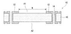
図1から図3は、本発明の一実施例に係るコア基板のキャビティ加工方法を示す図面である。図1から図3を参照すると、コア基板10、第1加工領域A1、第2加工領域A2、回路パターン12、ビア14、絶縁体16、レーザービームLが示されている。 1 to 3 are views illustrating a cavity processing method for a core substrate according to an embodiment of the present invention. 1 to 3, a
先ず、図1に示すように、コア基板10の一面、より具体的には絶縁体16の一面に回路パターン12により区画される第1加工領域A1を形成する。ここで、第1加工領域A1とは、レーザービームが直接照射される絶縁体16の一側表面をいう。このような第1加工領域A1は、絶縁体16の表面に形成された回路パターン12により区画される。すなわち、回路パターン12でカバーされていない領域である露出部分が第1加工領域A1となる。 First, as shown in FIG. 1, a first processing region A <b> 1 defined by the
絶縁体16の一面に回路パターン12を形成する方法としては、サブトラクティブ法(subtractive process)、アディティブ法(additive process)、インクジェット法(ink jet process)など様々な方法を用いることができる。 As a method of forming the
一方、絶縁体16の他面に、回路パターン12により区画される第2加工領域A2を形成する。第2加工領域A2は、第1加工領域A1と同様に、絶縁体16の下面に形成される回路パターン12により区画される部分であって、コア基板10の下面に形成された回路パターン12でカバーされていない領域である露出部分である。本実施例では、第2加工領域A2は、第1加工領域A1と対称に形成される。具体的に、第1加工領域A1と第2加工領域A2は絶縁体16を中心に対称位置に、同一大きさ及び同一形状に形成される。 On the other hand, a second processing region A2 defined by the
その他、絶縁体16の上下面に形成される回路パターン12は、絶縁体16を貫通するビア14により互いに電気的に接続されることができる。 In addition, the
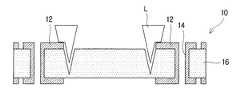
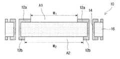
このように第1加工領域A1と第2加工領域A2を形成した後に、図2に示すように、レーザービームLを用いてコア基板10の一面から第1加工領域A1を全て除去してキャビティを加工する。このようにキャビティを加工すると、図3に示すように、キャビティの形状が回路パターン12により区画されるため、最初に設計した形状及び大きさWを有するキャビティを安定して確保することができる。すなわち、キャビティの大きさが回路パターン12により決定されることになる。これによって、キャビティの大きさの精度を向上させることができ、キャビティの内壁及び表面の加工品質も向上させることができる。図3には、回路パターン12により矩形の加工領域が区画され、それによって、四角柱状のキャビティが形成されたことが示されている。 After forming the first processing region A1 and the second processing region A2 in this way, as shown in FIG. 2, the first processing region A1 is completely removed from one surface of the
図4から図6は、本発明の他の実施例に係るコア基板10のキャビティ加工方法を示す図面である。本実施例は、上述した実施例と比較して場合、第2加工領域A2が第1加工領域A1よりも広く形成される点が異なっている。以下では、上述した実施例との相違点を中心に説明する。 4 to 6 are views illustrating a cavity processing method for the
本実施例によれば、図4に示すように、第2加工領域A2が第1加工領域A1よりも広く形成される。図4には、第1加工領域A1が「W1」の大きさを有し、第2加工領域A2が「W2」の大きさを有することが示されている。 According to this embodiment, as shown in FIG. 4, the second machining area A2 is formed wider than the first machining area A1. FIG. 4 shows that the first machining area A1 has a size of “W1” and the second machining area A2 has a size of “W2”.
このように、第2加工領域A2を第1加工領域A1より大きく設計して形成すると、コア基板10の上下面に回路パターン12a,12bを形成する過程で層間ずれが生じても、このずれによるキャビティの縮小を防止できるため、所望する大きさのキャビティを正確に加工することができる。図5には、レーザービームLを用いてキャビティを加工する方法が示されている。 As described above, when the second processing region A2 is designed and formed larger than the first processing region A1, even if an interlayer shift occurs in the process of forming the
図6は、層間ずれによりキャビティの大きさが縮小された場合を示している。図6に示すように、コア基板10の上下回路パターン12間にずれが生じる場合、キャビティの傾斜により、設計時のキャビティの大きさW1よりも小さい大きさW3を有するキャビティが形成される。すなわち、電子素子20が内蔵される空間が縮小されてしまうことになる。 FIG. 6 shows a case where the size of the cavity is reduced due to interlayer displacement. As shown in FIG. 6, when a deviation occurs between the upper and
このような問題を解決するために、本実施例によれば、第2加工領域A2を第1加工領域A1よりも大きく形成することにより、図7に示すように、ずれが生じても第1加工領域A1と第2加工領域A2との大きさの差によりずれが補正可能となり、設計時のキャビティの大きさを確保することができる。 In order to solve such a problem, according to the present embodiment, by forming the second processing region A2 larger than the first processing region A1, even if a shift occurs as shown in FIG. The shift can be corrected by the difference in size between the machining area A1 and the second machining area A2, and the size of the cavity at the time of design can be ensured.
一方、回路パターン12a,12bのずれは、X−Y全方向に亘って生じる可能性があり、これを十分に補完するために、第1加工領域A1の中心と第2加工領域A2の中心とを同一垂直線上に位置させることができる。図8の(a)は、第1加工領域A1の中心と第2加工領域A2の中心が重なっていることを示している。 On the other hand, the displacement of the
さらに、第1加工領域A1と第2加工領域A2とを同一形状にすることにより、回路パターン12a,12bが全方向にずれることをより十分に補完することもできる。図8の(a)及び(b)は、第1加工領域A1と第2加工領域A2が両方とも正四角形状を有する場合を示している。 Further, by making the first machining area A1 and the second machining area A2 the same shape, it is possible to more fully compensate for the
次に、本発明の他の実施形態に係る電子素子内蔵型印刷回路基板について説明する。 Next, an electronic element built-in type printed circuit board according to another embodiment of the present invention will be described.
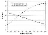
図9は、電子素子及び絶縁層が積層された状態における応力評価のためのモデリング図面であり、図10は、絶縁層の厚さによって変化する応力を示すグラフであり、図11は、絶縁層の厚さによって変化する反り程度を示すグラフであり、図12は本発明の好ましい一実施例に係る電子素子内蔵型印刷回路基板を示す概念図である。 FIG. 9 is a modeling diagram for stress evaluation in a state in which an electronic element and an insulating layer are stacked, FIG. 10 is a graph showing a stress that varies depending on the thickness of the insulating layer, and FIG. FIG. 12 is a conceptual diagram illustrating a printed circuit board with a built-in electronic element according to a preferred embodiment of the present invention.
本実施例では、繰り返し熱応力環境下でも、反り現象が最小化になる超薄型、高信頼性の電子素子内蔵型印刷回路基板を実現するために、幾何学的に対称構造となる電子素子の内蔵構造と、このための電子素子の内蔵方法を特徴とする。基板の熱応力環境下での反り現象は、用いられる資材の熱膨張係数(CTE)、弾性係数(Young's modulus)、ポアソン比(Poisson ratio)などの物性値と幾何学的因子(Geometric factor)により決定される。これを計算するために、図9のような印刷回路基板モデルを例に挙げると、中心軸(Neutral Line)は式(1)のように表される。
式(1)から計算される基板の曲げモーメント(bending moment、M;単位:Nm)及び水平荷重(normal force、N;単位:N)は式(2)のように表される。
式(2)から計算される構成行列(Compliance matrix)は式(3)のようになる。
式(3)から計算される剛性行列(Stiffness matrix)は式(4)のようになる。
式(4)から計算されるABD行列(ABD matrix)は式(5)のようになる。
式(5)から計算される基板の変形率(strain)と曲率(curvature)はそれぞれ式(6)の行列により得ることができる。
式(6)の計算から得られた応力評価(Stress Evaluation)の結果は、式(7)のようになる。
これをグラフに表すと図10のようになる。具体的に、図10は、電子素子の厚さを100μmに固定したとき、絶縁層の厚さによって変化する基板の上部(top)と下部(bottom)における応力変化を示したものである。 This is shown in a graph in FIG. Specifically, FIG. 10 shows the stress change at the top and bottom of the substrate, which varies with the thickness of the insulating layer, when the thickness of the electronic element is fixed at 100 μm.
また、反りの程度を基準として絶縁層の厚さに対する電子素子の厚さの依存性で計算した結果をグラフに表すと図11のようになる。具体的に、図11は、電子素子の厚さをそれぞれ50μm及び100μmに固定したとき、絶縁層の厚さによって変化する基板の反りの程度を示したものである。 FIG. 11 is a graph showing the result of calculation based on the dependence of the thickness of the electronic element on the thickness of the insulating layer based on the degree of warpage. Specifically, FIG. 11 shows the degree of warpage of the substrate that varies depending on the thickness of the insulating layer when the thickness of the electronic element is fixed to 50 μm and 100 μm, respectively.
図11において、絶縁層の厚さが50μmであるとき、ICの厚さが50μmである場合の反りは約0.26mmであり、ICの厚さが100μmで、2倍増加した場合の反りは約0.09mmであって約1/3に減少することから、基板の反り現象は絶縁層の厚さよりも電子素子の厚さに大きく依存していることが分かる。これにより、幾何学的に非対称的な構造を有する印刷回路基板において電子素子の薄型化に伴って基板全体の厚さを薄くすることはできないほど反り現象が増大すると予想される。 In FIG. 11, when the thickness of the insulating layer is 50 μm, the warpage when the thickness of the IC is 50 μm is about 0.26 mm, and the warpage when the thickness of the IC is 100 μm and increases twice. Since it is about 0.09 mm and is reduced to about 1/3, it can be seen that the warping phenomenon of the substrate is more dependent on the thickness of the electronic element than the thickness of the insulating layer. As a result, it is expected that the warpage phenomenon increases in the printed circuit board having a geometrically asymmetric structure as the thickness of the electronic element cannot be reduced as the electronic element becomes thinner.
これを解決するために、電子素子を基板の絶縁層に対して中央に位置させることにより幾何学的対称性を与えて反りを最小化しなければならない。したがって、本実施例では、電子素子内蔵型印刷回路基板に幾何学的対称性を与えることにより、繰り返し熱応力環境下でも反りが最小化になる超薄型、高信頼性の電子素子内蔵型印刷回路基板を実現することができる。 To solve this, the electronic element must be centered with respect to the insulating layer of the substrate to provide geometric symmetry and minimize warpage. Therefore, in this embodiment, by providing geometric symmetry to the printed circuit board with built-in electronic elements, the ultra-thin and highly reliable printed circuit with built-in electronic elements that minimizes warpage even under repeated thermal stress environments. A circuit board can be realized.
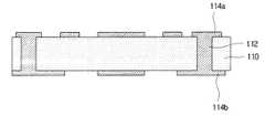
図12は本発明の一実施例に係る電子素子内蔵型印刷回路基板100を示す断面図である。本実施例に係る電子素子内蔵型印刷回路基板100は、図12に示すように、キャビティ116が形成されたコア基板110と、上記キャビティ116にフェースアップ(face-up)方式で内蔵され、表面に電極122が形成された電子素子120と、コア基板110の上面に積層された第1絶縁層130aと、上記コア基板110の下面に積層され、上記第1絶縁層130aと同一厚さを有する第2絶縁層130bと、を含む。ここで、電極122の厚さを含む上記電子素子の厚さbは、コア基板110の厚さと同一である。 FIG. 12 is a cross-sectional view illustrating a printed
ここで、「同一」とは、数学的に完全一致のみを意味するのみならず、設計誤差、製造誤差、測定誤差などを鑑みて実質的に同一であることを意味する。以下、本明細書における他の寸法及び位置などを「同一」という場合も同様である。 Here, “same” means not only mathematically a complete match, but also substantially the same in view of design error, manufacturing error, measurement error, and the like. Hereinafter, the same applies to the case where other dimensions and positions in the present specification are referred to as “same”.
本実施例に係る電子素子内蔵型印刷回路基板100は、内蔵される電子素子120を中心に対称構造に設計・製造されるため、基板の反りを最小化することができる構造である。さらに、電極122の厚さを含む電子素子120の厚さbを、コア基板110の厚さと同一に設計することにより、コア基板110自体の対称性を確保することができ、その結果、電子素子120が内蔵されたコア基板110の反りを最小化することができる。すなわち、コア基板110の上下対称性を実現するにおいて、電子素子120の表面に形成される電極122の厚さまで考慮してコア基板110自体の対称性を最大限に確保することである。このような対称構造によれば、印刷回路基板及びそれに内蔵される電子素子120の厚さが薄型化するに伴って反りが増大する危険性を低減させることが可能性となる。 The printed
また、コア基板110に内蔵される電子素子120をフェースアップ方式で実装することにより、回路の位置合わせ精度を容易に高めることができる。実際に、印刷回路基板において上面と下面の位置合わせ精度の差は少なくとも20μm〜50μm程度発生するが、本実施例のように、フェースアップ方式で電子素子120を内蔵することにより、電極122が上部に位置して、電子素子の電極と基板回路の位置合わせ精度を改善することができる。 In addition, the circuit alignment accuracy can be easily increased by mounting the
コア基板110の表面に内層回路114a,114bが形成される場合、電極122の厚さを含む電子素子120の厚さbを、内層回路114a,114bの厚さを含むコア基板110の厚さaと同一に設計することもできる。 When the
一方、電子素子120の水平方向の両側面からキャビティ116の内壁までの距離の和は、少なくとも60μm以上にしなければならない。キャビティ116は穿孔やレーザーなどで加工し、また電子素子120の場合もダイシング過程でチッピング(Chipping)が発生することがあるため、距離の基準はそれぞれの凹凸の界面における最外郭線を基準とする。 On the other hand, the sum of the distances from the both side surfaces of the
電子素子120と内壁との間隔は、設計値を基準として片側30μm程度が最小値であるが、実際には、設備のトレランス(Tolerance)のために電子素子120が一側内壁に接する場合も発生する。したがって、図12の「c」と「d」の各範囲は、0〜60μm程度の値を有することができ、「c+d」の値が60μm以上になることがよい。 The minimum distance between the
片側の距離を50μm以下に設計した場合は、電子素子120がキャビティ116に完全に収容されず、一側内壁に乗り上げた状態となり、シミュレーションと実測データによれば、キャビティ116が大きくなるほど、基板の反り現象は低減する傾向があった。ただし、キャビティ116が広くなりすぎると、回路空間を確保しにくくなる問題があるため、「c+d」の最大値は160μm以下にすることがよい。 When the distance on one side is designed to be 50 μm or less, the
以上では、本発明の一実施例に係る電子素子内蔵型印刷回路基板の構造について説明したが、以下では上記電子素子内蔵型印刷回路基板を製造する方法について図13から図19を参照して説明する。本発明の一実施例に係る電子素子内蔵型印刷回路基板の構造は、上述した通りであるため、以下では構造的な特徴に関する説明は省略し、製造工程を中心に説明する。 The structure of the printed circuit board with a built-in electronic element according to an embodiment of the present invention has been described above, but a method for manufacturing the printed circuit board with a built-in electronic element will be described below with reference to FIGS. To do. The structure of a printed circuit board with a built-in electronic element according to an embodiment of the present invention is as described above, and therefore, description regarding structural features will be omitted below, and the description will focus on the manufacturing process.
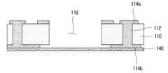
先ず、図13に示すように、コア基板110を用意する。コア基板110の表面には内層回路114a,114bを形成してもよく、この場合、コア基板110の上下面はビア112を介して電気的に接続することになる。 First, as shown in FIG. 13, a
次に、図14に示すように、コア基板110にキャビティ116を形成する。キャビティ116は、後で電子素子120が内蔵される領域であって、内蔵される電子素子120の大きさや形状を考慮して適切な大きさ及び形状に加工される。コア基板110にキャビティ116を加工するために、機械的ドリルまたはレーザードリルなどを用いることができる。 Next, as shown in FIG. 14, the
その後、図15に示すように、コア基板110の下面に接着層140を付着する。キャビティ116が形成されたコア基板110の下面に接着層140を付着すると、キャビティ116の下面は接着層140により遮蔽される。 Thereafter, as shown in FIG. 15, an
次に、図16に示すように、キャビティ116の露出している接着層140の表面に電子素子120をフェースアップ方式で付着し、その後、図17に示すように、コア基板110の上面に第1絶縁層130aを積層して電子素子120をカバーする。コア基板110の上面に積層される第1絶縁層130aにより、電子素子120が内蔵されたキャビティ116の内部も充填される。 Next, as shown in FIG. 16, the
その後、図18に示すように、コア基板110の下面に付着された接着層140を除去し、コア基板110の下面に第2絶縁層130bを積層する。 Thereafter, as shown in FIG. 18, the
次に、図19に示すように、第1絶縁層130a及び第2絶縁層130bに回路パターン132a,132b及びビア134a,134bを形成する。 Next, as shown in FIG. 19,
以上、本発明を実施の形態を用いて説明したが、本発明の技術的範囲は上記実施の形態に記載の範囲には限定されない。上記実施の形態に、多様な変更または改良を加えることが可能であることが当業者に明らかである。その様な変更または改良を加えた形態も本発明の技術的範囲に含まれ得ることが、特許請求の範囲の記載から明らかである。 As mentioned above, although this invention was demonstrated using embodiment, the technical scope of this invention is not limited to the range as described in the said embodiment. It will be apparent to those skilled in the art that various modifications or improvements can be added to the above-described embodiment. It is apparent from the scope of the claims that the embodiments added with such changes or improvements can be included in the technical scope of the present invention.
10 コア基板
A1 第1加工領域
A2 第2加工領域
12,12a,12b 回路パターン
14 ビア
16 絶縁体
20 電子素子
110 コア基板
112 ビア
114a,114b 内層回路
116 キャビティ
120 電子素子
122 電極
130a,130b 絶縁層
134a,134b ビアDESCRIPTION OF
Claims (7)
Translated fromJapanese前記コア基板の他面に、回路パターンにより区画される第2加工領域を形成する工程と、
前記コア基板の一面から前記第1加工領域を全て除去してキャビティを加工する工程と
を含むコア基板のキャビティ加工方法。Forming a first processing region partitioned by a circuit pattern on one surface of the core substrate;
Forming a second processing region partitioned by a circuit pattern on the other surface of the core substrate;
Removing the entire first processing region from one surface of the core substrate and processing the cavity.
前記コア基板を貫通するキャビティと、
表面に電極が形成され、前記キャビティにフェースアップ方式で内蔵される電子素子と、
前記コア基板の一面に積層される第1絶縁層と、
前記コア基板の他面に積層され、前記第1絶縁層と同一厚さを有する第2絶縁層と
を含み、
前記電極の厚さを含む前記電子素子の厚さは、前記コア基板の厚さと同一であることを特徴とする電子素子内蔵型印刷回路基板。A core substrate;
A cavity penetrating the core substrate;
An electrode formed on the surface and embedded in the cavity in a face-up manner;
A first insulating layer laminated on one surface of the core substrate;
A second insulating layer laminated on the other surface of the core substrate and having the same thickness as the first insulating layer;
The electronic device-embedded printed circuit board, wherein a thickness of the electronic device including a thickness of the electrode is the same as a thickness of the core substrate.
前記電極の厚さを含む前記電子素子の厚さは、前記内層回路の厚さを含む前記コア基板の厚さと同一であることを特徴とする請求項5に記載の電子素子内蔵型印刷回路基板。An inner layer circuit is formed on the surface of the core substrate,
6. The printed circuit board with built-in electronic device according to claim 5, wherein the thickness of the electronic device including the thickness of the electrode is the same as the thickness of the core substrate including the thickness of the inner layer circuit. .
Applications Claiming Priority (4)
| Application Number | Priority Date | Filing Date | Title |
|---|---|---|---|
| KR1020090078738AKR20110021123A (en) | 2009-08-25 | 2009-08-25 | Electronic printed circuit board |
| KR10-2009-0078738 | 2009-08-25 | ||
| KR1020090102504AKR101107067B1 (en) | 2009-10-27 | 2009-10-27 | Method for processing cavity of core substrate |
| KR10-2009-0102504 | 2009-10-27 |
Related Child Applications (1)
| Application Number | Title | Priority Date | Filing Date |
|---|---|---|---|
| JP2012195408ADivisionJP2012235175A (en) | 2009-08-25 | 2012-09-05 | Electronic element built-in printed circuit board |
Publications (2)
| Publication Number | Publication Date |
|---|---|
| JP2011049555Atrue JP2011049555A (en) | 2011-03-10 |
| JP5200249B2 JP5200249B2 (en) | 2013-06-05 |
Family
ID=43623157
Family Applications (2)
| Application Number | Title | Priority Date | Filing Date |
|---|---|---|---|
| JP2010178924AActiveJP5200249B2 (en) | 2009-08-25 | 2010-08-09 | Cavity processing method for core substrate |
| JP2012195408APendingJP2012235175A (en) | 2009-08-25 | 2012-09-05 | Electronic element built-in printed circuit board |
Family Applications After (1)
| Application Number | Title | Priority Date | Filing Date |
|---|---|---|---|
| JP2012195408APendingJP2012235175A (en) | 2009-08-25 | 2012-09-05 | Electronic element built-in printed circuit board |
Country Status (4)
| Country | Link |
|---|---|
| US (2) | US8633397B2 (en) |
| JP (2) | JP5200249B2 (en) |
| CN (1) | CN101998772B (en) |
| TW (1) | TWI418272B (en) |
Cited By (4)
| Publication number | Priority date | Publication date | Assignee | Title |
|---|---|---|---|---|
| JP2013055109A (en)* | 2011-09-01 | 2013-03-21 | Fujikura Ltd | Substrate with built-in component and method for manufacturing the same |
| JP2015065400A (en)* | 2013-09-25 | 2015-04-09 | サムソン エレクトロ−メカニックス カンパニーリミテッド. | Element embedded printed circuit board and method of manufacturing the same |
| JP2016111332A (en)* | 2014-12-02 | 2016-06-20 | 旭徳科技股▲ふん▼有限公司 | Packaging structure and manufacturing method thereof |
| US10383231B2 (en) | 2013-02-08 | 2019-08-13 | Fujikura Ltd. | Component-embedded board and method of manufacturing same |
Families Citing this family (29)
| Publication number | Priority date | Publication date | Assignee | Title |
|---|---|---|---|---|
| KR101283821B1 (en)* | 2011-05-03 | 2013-07-08 | 엘지이노텍 주식회사 | The method for manufacturing the printed circuit board |
| US20130256007A1 (en)* | 2012-03-28 | 2013-10-03 | Ibiden Co., Ltd. | Wiring board with built-in electronic component and method for manufacturing the same |
| CN103635023B (en)* | 2012-08-27 | 2016-08-24 | 富葵精密组件(深圳)有限公司 | The manufacture method of circuit board |
| KR20140042604A (en)* | 2012-09-28 | 2014-04-07 | 엘지이노텍 주식회사 | Printed circuit board and method for manufacturing same |
| KR20140081193A (en)* | 2012-12-21 | 2014-07-01 | 삼성전기주식회사 | Hybrid substrate with high density and low density substrate area and manufacturing method thereof |
| US9288917B2 (en)* | 2013-11-07 | 2016-03-15 | Unimicron Technology Corp. | Manufacturing method for multi-layer circuit board |
| KR102466204B1 (en)* | 2015-12-16 | 2022-11-11 | 삼성전기주식회사 | Printed circuit board and method of manufacturing the same |
| JP6637608B2 (en)* | 2016-09-09 | 2020-01-29 | 株式会社フジクラ | Component-embedded substrate and manufacturing method thereof |
| CN107222972A (en)* | 2017-06-14 | 2017-09-29 | 鹤山市中富兴业电路有限公司 | A kind of PCB construction and its manufacture craft for being embedded with passive device |
| KR20190075647A (en)* | 2017-12-21 | 2019-07-01 | 삼성전자주식회사 | Fan-out semiconductor package |
| EP3621107B1 (en)* | 2018-09-10 | 2025-03-26 | AT & S Austria Technologie & Systemtechnik Aktiengesellschaft | Component with dielectric layer for embedding in component carrier |
| US11342256B2 (en) | 2019-01-24 | 2022-05-24 | Applied Materials, Inc. | Method of fine redistribution interconnect formation for advanced packaging applications |
| US11277917B2 (en)* | 2019-03-12 | 2022-03-15 | Advanced Semiconductor Engineering, Inc. | Embedded component package structure, embedded type panel substrate and manufacturing method thereof |
| IT201900006740A1 (en)* | 2019-05-10 | 2020-11-10 | Applied Materials Inc | SUBSTRATE STRUCTURING PROCEDURES |
| IT201900006736A1 (en) | 2019-05-10 | 2020-11-10 | Applied Materials Inc | PACKAGE MANUFACTURING PROCEDURES |
| US11931855B2 (en) | 2019-06-17 | 2024-03-19 | Applied Materials, Inc. | Planarization methods for packaging substrates |
| CN112770495B (en)* | 2019-10-21 | 2022-05-27 | 宏启胜精密电子(秦皇岛)有限公司 | Omnidirectional embedded module and manufacturing method thereof, and packaging structure and manufacturing method thereof |
| US11862546B2 (en) | 2019-11-27 | 2024-01-02 | Applied Materials, Inc. | Package core assembly and fabrication methods |
| US11257790B2 (en) | 2020-03-10 | 2022-02-22 | Applied Materials, Inc. | High connectivity device stacking |
| US11454884B2 (en) | 2020-04-15 | 2022-09-27 | Applied Materials, Inc. | Fluoropolymer stamp fabrication method |
| US11400545B2 (en) | 2020-05-11 | 2022-08-02 | Applied Materials, Inc. | Laser ablation for package fabrication |
| US11232951B1 (en) | 2020-07-14 | 2022-01-25 | Applied Materials, Inc. | Method and apparatus for laser drilling blind vias |
| US11676832B2 (en) | 2020-07-24 | 2023-06-13 | Applied Materials, Inc. | Laser ablation system for package fabrication |
| CN114449781B (en)* | 2020-10-30 | 2024-11-15 | 庆鼎精密电子(淮安)有限公司 | Method for manufacturing circuit board with embedded components |
| US11521937B2 (en) | 2020-11-16 | 2022-12-06 | Applied Materials, Inc. | Package structures with built-in EMI shielding |
| US11404318B2 (en) | 2020-11-20 | 2022-08-02 | Applied Materials, Inc. | Methods of forming through-silicon vias in substrates for advanced packaging |
| US11705365B2 (en) | 2021-05-18 | 2023-07-18 | Applied Materials, Inc. | Methods of micro-via formation for advanced packaging |
| US12183684B2 (en) | 2021-10-26 | 2024-12-31 | Applied Materials, Inc. | Semiconductor device packaging methods |
| CN117794082A (en)* | 2024-01-08 | 2024-03-29 | 沪士电子股份有限公司 | Printed circuit board and preparation method thereof |
Citations (5)
| Publication number | Priority date | Publication date | Assignee | Title |
|---|---|---|---|---|
| JP2007266195A (en)* | 2006-03-28 | 2007-10-11 | Dainippon Printing Co Ltd | Multilayer printed wiring board and manufacturing method thereof |
| JP2007318090A (en)* | 2006-04-25 | 2007-12-06 | Ngk Spark Plug Co Ltd | Method for manufacturing wiring board |
| JP2008034589A (en)* | 2006-07-28 | 2008-02-14 | Dainippon Printing Co Ltd | Multilayer printed wiring board and manufacturing method thereof |
| JP2008306173A (en)* | 2007-05-07 | 2008-12-18 | Ngk Spark Plug Co Ltd | Wiring board with built-in component and method for manufacturing same |
| JP2009105345A (en)* | 2007-10-25 | 2009-05-14 | Ngk Spark Plug Co Ltd | Wiring substrate with built-in plate-like component |
Family Cites Families (16)
| Publication number | Priority date | Publication date | Assignee | Title |
|---|---|---|---|---|
| JPH0955459A (en)* | 1995-06-06 | 1997-02-25 | Seiko Epson Corp | Semiconductor device |
| US5841193A (en)* | 1996-05-20 | 1998-11-24 | Epic Technologies, Inc. | Single chip modules, repairable multichip modules, and methods of fabrication thereof |
| US5889654A (en)* | 1997-04-09 | 1999-03-30 | International Business Machines Corporation | Advanced chip packaging structure for memory card applications |
| US6538210B2 (en)* | 1999-12-20 | 2003-03-25 | Matsushita Electric Industrial Co., Ltd. | Circuit component built-in module, radio device having the same, and method for producing the same |
| JP4160439B2 (en) | 2003-04-22 | 2008-10-01 | 日立ビアメカニクス株式会社 | Laser drilling method |
| TWI241007B (en)* | 2004-09-09 | 2005-10-01 | Phoenix Prec Technology Corp | Semiconductor device embedded structure and method for fabricating the same |
| KR100688769B1 (en)* | 2004-12-30 | 2007-03-02 | 삼성전기주식회사 | Chip embedded printed circuit board by plating and manufacturing method thereof |
| TWI269361B (en)* | 2005-06-17 | 2006-12-21 | Advanced Semiconductor Eng | Structure of substrate integrated embedded passive component and method of forming the same |
| US8335084B2 (en)* | 2005-08-01 | 2012-12-18 | Georgia Tech Research Corporation | Embedded actives and discrete passives in a cavity within build-up layers |
| KR100697980B1 (en) | 2005-09-12 | 2007-03-23 | 삼성전기주식회사 | Manufacturing method of printed circuit board containing electronic components |
| US8101868B2 (en)* | 2005-10-14 | 2012-01-24 | Ibiden Co., Ltd. | Multilayered printed circuit board and method for manufacturing the same |
| KR100758229B1 (en) | 2006-04-11 | 2007-09-12 | 삼성전기주식회사 | Electronic circuit board and manufacturing method |
| US20080054443A1 (en)* | 2006-08-23 | 2008-03-06 | Chao-Wen Shih | Carrier board structure with semiconductor chip embedded therein |
| JP2008277392A (en)* | 2007-04-26 | 2008-11-13 | Kyocera Corp | Component built-in substrate and manufacturing method thereof |
| KR100821154B1 (en)* | 2007-07-11 | 2008-04-14 | 삼성전기주식회사 | Electronic circuit board and manufacturing method |
| TWI338941B (en)* | 2007-08-22 | 2011-03-11 | Unimicron Technology Corp | Semiconductor package structure |
- 2010
- 2010-07-26TWTW099124561Apatent/TWI418272B/ennot_activeIP Right Cessation
- 2010-08-09JPJP2010178924Apatent/JP5200249B2/enactiveActive
- 2010-08-20USUS12/860,301patent/US8633397B2/enactiveActive - Reinstated
- 2010-08-25CNCN2010102632578Apatent/CN101998772B/ennot_activeExpired - Fee Related
- 2012
- 2012-09-05JPJP2012195408Apatent/JP2012235175A/enactivePending
- 2014
- 2014-01-09USUS14/151,577patent/US20140123486A1/ennot_activeAbandoned
Patent Citations (5)
| Publication number | Priority date | Publication date | Assignee | Title |
|---|---|---|---|---|
| JP2007266195A (en)* | 2006-03-28 | 2007-10-11 | Dainippon Printing Co Ltd | Multilayer printed wiring board and manufacturing method thereof |
| JP2007318090A (en)* | 2006-04-25 | 2007-12-06 | Ngk Spark Plug Co Ltd | Method for manufacturing wiring board |
| JP2008034589A (en)* | 2006-07-28 | 2008-02-14 | Dainippon Printing Co Ltd | Multilayer printed wiring board and manufacturing method thereof |
| JP2008306173A (en)* | 2007-05-07 | 2008-12-18 | Ngk Spark Plug Co Ltd | Wiring board with built-in component and method for manufacturing same |
| JP2009105345A (en)* | 2007-10-25 | 2009-05-14 | Ngk Spark Plug Co Ltd | Wiring substrate with built-in plate-like component |
Cited By (4)
| Publication number | Priority date | Publication date | Assignee | Title |
|---|---|---|---|---|
| JP2013055109A (en)* | 2011-09-01 | 2013-03-21 | Fujikura Ltd | Substrate with built-in component and method for manufacturing the same |
| US10383231B2 (en) | 2013-02-08 | 2019-08-13 | Fujikura Ltd. | Component-embedded board and method of manufacturing same |
| JP2015065400A (en)* | 2013-09-25 | 2015-04-09 | サムソン エレクトロ−メカニックス カンパニーリミテッド. | Element embedded printed circuit board and method of manufacturing the same |
| JP2016111332A (en)* | 2014-12-02 | 2016-06-20 | 旭徳科技股▲ふん▼有限公司 | Packaging structure and manufacturing method thereof |
Also Published As
| Publication number | Publication date |
|---|---|
| US20140123486A1 (en) | 2014-05-08 |
| US20110048780A1 (en) | 2011-03-03 |
| CN101998772A (en) | 2011-03-30 |
| JP2012235175A (en) | 2012-11-29 |
| TWI418272B (en) | 2013-12-01 |
| TW201112897A (en) | 2011-04-01 |
| JP5200249B2 (en) | 2013-06-05 |
| CN101998772B (en) | 2013-03-27 |
| US8633397B2 (en) | 2014-01-21 |
Similar Documents
| Publication | Publication Date | Title |
|---|---|---|
| JP5200249B2 (en) | Cavity processing method for core substrate | |
| JP6427817B2 (en) | Printed circuit board and manufacturing method thereof | |
| JP6969557B2 (en) | Through Silicon Via Board and Mounting Board | |
| JP5827166B2 (en) | Wiring board and method of manufacturing wiring board | |
| JP2007207781A (en) | Multilayer printed wiring board and method for manufacturing printed wiring board | |
| US12019111B2 (en) | Manufacturing method of a multi-layer for a probe card | |
| JP2016111221A (en) | Method of manufacturing wiring board and wiring board | |
| CN111696930A (en) | Embedded element packaging structure, embedded surface packaging substrate and manufacturing method thereof | |
| CN101849284B (en) | Structure for reducing substrate warpage | |
| JP2015231005A (en) | Wiring board and manufacturing method of the same | |
| US20160071807A1 (en) | Methodology to achieve zero warpage for ic package | |
| KR20190068641A (en) | Delayed via formation in electronic devices | |
| US20090265028A1 (en) | Organic Substrate with Asymmetric Thickness for Warp Mitigation | |
| JP2009016806A (en) | Embedded pattern board and its manufacturing method | |
| JP2017076763A (en) | Wiring board and manufacturing method therefor | |
| JP4899548B2 (en) | Manufacturing method of semiconductor device | |
| JP2013183002A (en) | Electronic component | |
| JP4452846B2 (en) | Metal-ceramic bonding substrate and manufacturing method thereof | |
| KR20150028031A (en) | Printed circuit board | |
| JP2013008910A (en) | Wiring board and method for manufacturing wiring board | |
| Ding et al. | Molding process development for high density I/Os Fan-Out Wafer Level Package (FOWLP) with fine pitch RDL | |
| KR20110021123A (en) | Electronic printed circuit board | |
| JP2010263035A (en) | Method for manufacturing printed wiring board | |
| KR101748237B1 (en) | Improving Method for Bending Printed Circuit Board | |
| JP2008010709A (en) | Method of manufacturing circuit board |
Legal Events
| Date | Code | Title | Description |
|---|---|---|---|
| A977 | Report on retrieval | Free format text:JAPANESE INTERMEDIATE CODE: A971007 Effective date:20120525 | |
| A131 | Notification of reasons for refusal | Free format text:JAPANESE INTERMEDIATE CODE: A131 Effective date:20120605 | |
| A521 | Request for written amendment filed | Free format text:JAPANESE INTERMEDIATE CODE: A523 Effective date:20120905 | |
| TRDD | Decision of grant or rejection written | ||
| A01 | Written decision to grant a patent or to grant a registration (utility model) | Free format text:JAPANESE INTERMEDIATE CODE: A01 Effective date:20130115 | |
| A61 | First payment of annual fees (during grant procedure) | Free format text:JAPANESE INTERMEDIATE CODE: A61 Effective date:20130117 | |
| R150 | Certificate of patent or registration of utility model | Free format text:JAPANESE INTERMEDIATE CODE: R150 Ref document number:5200249 Country of ref document:JP Free format text:JAPANESE INTERMEDIATE CODE: R150 | |
| FPAY | Renewal fee payment (event date is renewal date of database) | Free format text:PAYMENT UNTIL: 20160222 Year of fee payment:3 | |
| R250 | Receipt of annual fees | Free format text:JAPANESE INTERMEDIATE CODE: R250 | |
| R250 | Receipt of annual fees | Free format text:JAPANESE INTERMEDIATE CODE: R250 | |
| R250 | Receipt of annual fees | Free format text:JAPANESE INTERMEDIATE CODE: R250 | |
| R250 | Receipt of annual fees | Free format text:JAPANESE INTERMEDIATE CODE: R250 | |
| R250 | Receipt of annual fees | Free format text:JAPANESE INTERMEDIATE CODE: R250 | |
| R250 | Receipt of annual fees | Free format text:JAPANESE INTERMEDIATE CODE: R250 | |
| R250 | Receipt of annual fees | Free format text:JAPANESE INTERMEDIATE CODE: R250 | |
| R250 | Receipt of annual fees | Free format text:JAPANESE INTERMEDIATE CODE: R250 | |
| R250 | Receipt of annual fees | Free format text:JAPANESE INTERMEDIATE CODE: R250 |