JP2011049398A - Laser irradiation device and manufacturing method of semiconductor substrate - Google Patents
Laser irradiation device and manufacturing method of semiconductor substrateDownload PDFInfo
- Publication number
- JP2011049398A JP2011049398AJP2009197200AJP2009197200AJP2011049398AJP 2011049398 AJP2011049398 AJP 2011049398AJP 2009197200 AJP2009197200 AJP 2009197200AJP 2009197200 AJP2009197200 AJP 2009197200AJP 2011049398 AJP2011049398 AJP 2011049398A
- Authority
- JP
- Japan
- Prior art keywords
- laser
- semiconductor
- substrate
- layer
- semiconductor film
- Prior art date
- Legal status (The legal status is an assumption and is not a legal conclusion. Google has not performed a legal analysis and makes no representation as to the accuracy of the status listed.)
- Granted
Links
- 239000004065semiconductorSubstances0.000titleclaimsabstractdescription240
- 239000000758substrateSubstances0.000titleclaimsdescription133
- 238000004519manufacturing processMethods0.000titleclaimsdescription17
- 230000003287optical effectEffects0.000claimsabstractdescription29
- 239000012535impuritySubstances0.000claimsdescription90
- XUIMIQQOPSSXEZ-UHFFFAOYSA-NSiliconChemical compound[Si]XUIMIQQOPSSXEZ-UHFFFAOYSA-N0.000claimsdescription40
- 229910052710siliconInorganic materials0.000claimsdescription40
- 239000010703siliconSubstances0.000claimsdescription40
- 238000012545processingMethods0.000claimsdescription39
- 239000000463materialSubstances0.000claimsdescription30
- OKTJSMMVPCPJKN-UHFFFAOYSA-NCarbonChemical compound[C]OKTJSMMVPCPJKN-UHFFFAOYSA-N0.000claimsdescription13
- 239000003463adsorbentSubstances0.000claimsdescription9
- 229910002804graphiteInorganic materials0.000claimsdescription8
- 239000010439graphiteSubstances0.000claimsdescription8
- 238000007493shaping processMethods0.000claims2
- 239000011358absorbing materialSubstances0.000abstract1
- 239000010410layerSubstances0.000description225
- 239000010408filmSubstances0.000description134
- 238000000034methodMethods0.000description48
- 239000013078crystalSubstances0.000description45
- 239000007789gasSubstances0.000description29
- 238000010438heat treatmentMethods0.000description29
- 150000002500ionsChemical class0.000description25
- 230000008018meltingEffects0.000description18
- 238000002844meltingMethods0.000description18
- 229910052581Si3N4Inorganic materials0.000description17
- HQVNEWCFYHHQES-UHFFFAOYSA-Nsilicon nitrideChemical compoundN12[Si]34N5[Si]62N3[Si]51N64HQVNEWCFYHHQES-UHFFFAOYSA-N0.000description17
- 239000012298atmosphereSubstances0.000description16
- 238000005468ion implantationMethods0.000description16
- 238000005530etchingMethods0.000description15
- VYPSYNLAJGMNEJ-UHFFFAOYSA-NSilicium dioxideChemical compoundO=[Si]=OVYPSYNLAJGMNEJ-UHFFFAOYSA-N0.000description14
- 230000007547defectEffects0.000description14
- 239000010936titaniumSubstances0.000description14
- 239000001257hydrogenSubstances0.000description13
- 229910052739hydrogenInorganic materials0.000description13
- 229910052782aluminiumInorganic materials0.000description12
- XAGFODPZIPBFFR-UHFFFAOYSA-NaluminiumChemical compound[Al]XAGFODPZIPBFFR-UHFFFAOYSA-N0.000description12
- 230000008569processEffects0.000description12
- 239000011521glassSubstances0.000description11
- 229910052719titaniumInorganic materials0.000description11
- 238000011282treatmentMethods0.000description11
- PXHVJJICTQNCMI-UHFFFAOYSA-NNickelChemical compound[Ni]PXHVJJICTQNCMI-UHFFFAOYSA-N0.000description10
- RTAQQCXQSZGOHL-UHFFFAOYSA-NTitaniumChemical compound[Ti]RTAQQCXQSZGOHL-UHFFFAOYSA-N0.000description10
- 230000006870functionEffects0.000description10
- 229910052814silicon oxideInorganic materials0.000description10
- 230000004888barrier functionEffects0.000description9
- 230000015572biosynthetic processEffects0.000description9
- 230000000694effectsEffects0.000description9
- IJGRMHOSHXDMSA-UHFFFAOYSA-NAtomic nitrogenChemical compoundN#NIJGRMHOSHXDMSA-UHFFFAOYSA-N0.000description8
- UFHFLCQGNIYNRP-UHFFFAOYSA-NHydrogenChemical compound[H][H]UFHFLCQGNIYNRP-UHFFFAOYSA-N0.000description8
- CSDREXVUYHZDNP-UHFFFAOYSA-NalumanylidynesiliconChemical compound[Al].[Si]CSDREXVUYHZDNP-UHFFFAOYSA-N0.000description8
- 239000002585baseSubstances0.000description8
- 229910052751metalInorganic materials0.000description8
- 239000002184metalSubstances0.000description8
- 238000009832plasma treatmentMethods0.000description8
- 238000011109contaminationMethods0.000description7
- 230000001678irradiating effectEffects0.000description7
- 229910052750molybdenumInorganic materials0.000description7
- 239000011733molybdenumSubstances0.000description7
- XKRFYHLGVUSROY-UHFFFAOYSA-NArgonChemical compound[Ar]XKRFYHLGVUSROY-UHFFFAOYSA-N0.000description6
- ZOKXTWBITQBERF-UHFFFAOYSA-NMolybdenumChemical compound[Mo]ZOKXTWBITQBERF-UHFFFAOYSA-N0.000description6
- 230000003647oxidationEffects0.000description6
- 238000007254oxidation reactionMethods0.000description6
- BASFCYQUMIYNBI-UHFFFAOYSA-NplatinumChemical compound[Pt]BASFCYQUMIYNBI-UHFFFAOYSA-N0.000description6
- 239000002356single layerSubstances0.000description6
- GQPLMRYTRLFLPF-UHFFFAOYSA-NNitrous OxideChemical compound[O-][N+]#NGQPLMRYTRLFLPF-UHFFFAOYSA-N0.000description5
- NRTOMJZYCJJWKI-UHFFFAOYSA-NTitanium nitrideChemical compound[Ti]#NNRTOMJZYCJJWKI-UHFFFAOYSA-N0.000description5
- 229910052799carbonInorganic materials0.000description5
- 150000001722carbon compoundsChemical class0.000description5
- 238000005229chemical vapour depositionMethods0.000description5
- 239000010949copperSubstances0.000description5
- 230000002349favourable effectEffects0.000description5
- 230000001590oxidative effectEffects0.000description5
- 239000001301oxygenSubstances0.000description5
- 229910052760oxygenInorganic materials0.000description5
- 238000005268plasma chemical vapour depositionMethods0.000description5
- 238000000926separation methodMethods0.000description5
- 229910021332silicideInorganic materials0.000description5
- FVBUAEGBCNSCDD-UHFFFAOYSA-Nsilicide(4-)Chemical compound[Si-4]FVBUAEGBCNSCDD-UHFFFAOYSA-N0.000description5
- 238000004544sputter depositionMethods0.000description5
- WFKWXMTUELFFGS-UHFFFAOYSA-NtungstenChemical compound[W]WFKWXMTUELFFGS-UHFFFAOYSA-N0.000description5
- 229910052721tungstenInorganic materials0.000description5
- 239000010937tungstenSubstances0.000description5
- ZOXJGFHDIHLPTG-UHFFFAOYSA-NBoronChemical compound[B]ZOXJGFHDIHLPTG-UHFFFAOYSA-N0.000description4
- CURLTUGMZLYLDI-UHFFFAOYSA-NCarbon dioxideChemical compoundO=C=OCURLTUGMZLYLDI-UHFFFAOYSA-N0.000description4
- 239000000956alloySubstances0.000description4
- QVGXLLKOCUKJST-UHFFFAOYSA-Natomic oxygenChemical compound[O]QVGXLLKOCUKJST-UHFFFAOYSA-N0.000description4
- 229910052796boronInorganic materials0.000description4
- 239000011651chromiumSubstances0.000description4
- KPUWHANPEXNPJT-UHFFFAOYSA-NdisiloxaneChemical class[SiH3]O[SiH3]KPUWHANPEXNPJT-UHFFFAOYSA-N0.000description4
- 238000009826distributionMethods0.000description4
- 229910052736halogenInorganic materials0.000description4
- 150000002367halogensChemical class0.000description4
- 238000010884ion-beam techniqueMethods0.000description4
- 229910021421monocrystalline siliconInorganic materials0.000description4
- 229910052759nickelInorganic materials0.000description4
- 229910052757nitrogenInorganic materials0.000description4
- 239000010453quartzSubstances0.000description4
- 229920005989resinPolymers0.000description4
- 239000011347resinSubstances0.000description4
- KDLHZDBZIXYQEI-UHFFFAOYSA-NPalladiumChemical compound[Pd]KDLHZDBZIXYQEI-UHFFFAOYSA-N0.000description3
- OAICVXFJPJFONN-UHFFFAOYSA-NPhosphorusChemical compound[P]OAICVXFJPJFONN-UHFFFAOYSA-N0.000description3
- 229910045601alloyInorganic materials0.000description3
- 229910052786argonInorganic materials0.000description3
- 150000001875compoundsChemical class0.000description3
- 229910052802copperInorganic materials0.000description3
- 238000002425crystallisationMethods0.000description3
- 230000008025crystallizationEffects0.000description3
- 238000010586diagramMethods0.000description3
- -1hydrogen ionsChemical class0.000description3
- 239000007943implantSubstances0.000description3
- 239000010955niobiumSubstances0.000description3
- 239000011368organic materialSubstances0.000description3
- 229910052698phosphorusInorganic materials0.000description3
- 239000011574phosphorusSubstances0.000description3
- HBMJWWWQQXIZIP-UHFFFAOYSA-Nsilicon carbideChemical compound[Si+]#[C-]HBMJWWWQQXIZIP-UHFFFAOYSA-N0.000description3
- 229910010271silicon carbideInorganic materials0.000description3
- 238000003746solid phase reactionMethods0.000description3
- 229910052715tantalumInorganic materials0.000description3
- GUVRBAGPIYLISA-UHFFFAOYSA-Ntantalum atomChemical compound[Ta]GUVRBAGPIYLISA-UHFFFAOYSA-N0.000description3
- 238000012546transferMethods0.000description3
- QGZKDVFQNNGYKY-UHFFFAOYSA-NAmmoniaChemical compoundNQGZKDVFQNNGYKY-UHFFFAOYSA-N0.000description2
- ZAMOUSCENKQFHK-UHFFFAOYSA-NChlorine atomChemical compound[Cl]ZAMOUSCENKQFHK-UHFFFAOYSA-N0.000description2
- VYZAMTAEIAYCRO-UHFFFAOYSA-NChromiumChemical compound[Cr]VYZAMTAEIAYCRO-UHFFFAOYSA-N0.000description2
- RYGMFSIKBFXOCR-UHFFFAOYSA-NCopperChemical compound[Cu]RYGMFSIKBFXOCR-UHFFFAOYSA-N0.000description2
- YCKRFDGAMUMZLT-UHFFFAOYSA-NFluorine atomChemical compound[F]YCKRFDGAMUMZLT-UHFFFAOYSA-N0.000description2
- 229910052779NeodymiumInorganic materials0.000description2
- 239000004642PolyimideSubstances0.000description2
- 230000001133accelerationEffects0.000description2
- 229910052783alkali metalInorganic materials0.000description2
- 150000001340alkali metalsChemical class0.000description2
- 229910052784alkaline earth metalInorganic materials0.000description2
- 150000001342alkaline earth metalsChemical class0.000description2
- 229910052785arsenicInorganic materials0.000description2
- RQNWIZPPADIBDY-UHFFFAOYSA-Narsenic atomChemical compound[As]RQNWIZPPADIBDY-UHFFFAOYSA-N0.000description2
- 229910002092carbon dioxideInorganic materials0.000description2
- 239000001569carbon dioxideSubstances0.000description2
- 239000000919ceramicSubstances0.000description2
- 230000008859changeEffects0.000description2
- 239000000460chlorineSubstances0.000description2
- 229910052801chlorineInorganic materials0.000description2
- 229910052804chromiumInorganic materials0.000description2
- 239000010941cobaltSubstances0.000description2
- 229910017052cobaltInorganic materials0.000description2
- GUTLYIVDDKVIGB-UHFFFAOYSA-Ncobalt atomChemical compound[Co]GUTLYIVDDKVIGB-UHFFFAOYSA-N0.000description2
- 238000004891communicationMethods0.000description2
- 239000004020conductorSubstances0.000description2
- 229910021419crystalline siliconInorganic materials0.000description2
- 238000001312dry etchingMethods0.000description2
- 238000007667floatingMethods0.000description2
- 229910052731fluorineInorganic materials0.000description2
- 239000011737fluorineSubstances0.000description2
- 239000010931goldSubstances0.000description2
- 239000001307heliumSubstances0.000description2
- 229910052734heliumInorganic materials0.000description2
- SWQJXJOGLNCZEY-UHFFFAOYSA-Nhelium atomChemical compound[He]SWQJXJOGLNCZEY-UHFFFAOYSA-N0.000description2
- 230000006872improvementEffects0.000description2
- 238000009616inductively coupled plasmaMethods0.000description2
- 239000012212insulatorSubstances0.000description2
- 239000007791liquid phaseSubstances0.000description2
- 239000011572manganeseSubstances0.000description2
- 230000004048modificationEffects0.000description2
- 238000012986modificationMethods0.000description2
- QEFYFXOXNSNQGX-UHFFFAOYSA-Nneodymium atomChemical compound[Nd]QEFYFXOXNSNQGX-UHFFFAOYSA-N0.000description2
- 238000005121nitridingMethods0.000description2
- MWUXSHHQAYIFBG-UHFFFAOYSA-Nnitrogen oxideInorganic materialsO=[N]MWUXSHHQAYIFBG-UHFFFAOYSA-N0.000description2
- 239000001272nitrous oxideSubstances0.000description2
- TWNQGVIAIRXVLR-UHFFFAOYSA-Noxo(oxoalumanyloxy)alumaneChemical compoundO=[Al]O[Al]=OTWNQGVIAIRXVLR-UHFFFAOYSA-N0.000description2
- 239000002245particleSubstances0.000description2
- 238000000059patterningMethods0.000description2
- 230000035515penetrationEffects0.000description2
- 229910052697platinumInorganic materials0.000description2
- 229920001721polyimidePolymers0.000description2
- 150000003254radicalsChemical class0.000description2
- 230000009467reductionEffects0.000description2
- 229910052594sapphireInorganic materials0.000description2
- 239000010980sapphireSubstances0.000description2
- 150000003376siliconChemical class0.000description2
- 239000007790solid phaseSubstances0.000description2
- 239000010935stainless steelSubstances0.000description2
- 229910001220stainless steelInorganic materials0.000description2
- VZGDMQKNWNREIO-UHFFFAOYSA-NtetrachloromethaneChemical compoundClC(Cl)(Cl)ClVZGDMQKNWNREIO-UHFFFAOYSA-N0.000description2
- 239000010409thin filmSubstances0.000description2
- JBRZTFJDHDCESZ-UHFFFAOYSA-NAsGaChemical compound[As]#[Ga]JBRZTFJDHDCESZ-UHFFFAOYSA-N0.000description1
- UGFAIRIUMAVXCW-UHFFFAOYSA-NCarbon monoxideChemical compound[O+]#[C-]UGFAIRIUMAVXCW-UHFFFAOYSA-N0.000description1
- 239000004593EpoxySubstances0.000description1
- GYHNNYVSQQEPJS-UHFFFAOYSA-NGalliumChemical compound[Ga]GYHNNYVSQQEPJS-UHFFFAOYSA-N0.000description1
- 229910001218Gallium arsenideInorganic materials0.000description1
- GPXJNWSHGFTCBW-UHFFFAOYSA-NIndium phosphideChemical compound[In]#PGPXJNWSHGFTCBW-UHFFFAOYSA-N0.000description1
- PWHULOQIROXLJO-UHFFFAOYSA-NManganeseChemical compound[Mn]PWHULOQIROXLJO-UHFFFAOYSA-N0.000description1
- CBENFWSGALASAD-UHFFFAOYSA-NOzoneChemical compound[O-][O+]=OCBENFWSGALASAD-UHFFFAOYSA-N0.000description1
- 239000004952PolyamideSubstances0.000description1
- BLRPTPMANUNPDV-UHFFFAOYSA-NSilaneChemical compound[SiH4]BLRPTPMANUNPDV-UHFFFAOYSA-N0.000description1
- 229910000577Silicon-germaniumInorganic materials0.000description1
- BQCADISMDOOEFD-UHFFFAOYSA-NSilverChemical compound[Ag]BQCADISMDOOEFD-UHFFFAOYSA-N0.000description1
- 229910002808Si–O–SiInorganic materials0.000description1
- 238000005411Van der Waals forceMethods0.000description1
- GDFCWFBWQUEQIJ-UHFFFAOYSA-N[B].[P]Chemical compound[B].[P]GDFCWFBWQUEQIJ-UHFFFAOYSA-N0.000description1
- LEVVHYCKPQWKOP-UHFFFAOYSA-N[Si].[Ge]Chemical compound[Si].[Ge]LEVVHYCKPQWKOP-UHFFFAOYSA-N0.000description1
- NIXOWILDQLNWCW-UHFFFAOYSA-Nacrylic acid groupChemical groupC(C=C)(=O)ONIXOWILDQLNWCW-UHFFFAOYSA-N0.000description1
- 239000003570airSubstances0.000description1
- 125000000217alkyl groupChemical group0.000description1
- PNEYBMLMFCGWSK-UHFFFAOYSA-Naluminium oxideInorganic materials[O-2].[O-2].[O-2].[Al+3].[Al+3]PNEYBMLMFCGWSK-UHFFFAOYSA-N0.000description1
- 239000005407aluminoborosilicate glassSubstances0.000description1
- 239000005354aluminosilicate glassSubstances0.000description1
- 229910021529ammoniaInorganic materials0.000description1
- 150000004945aromatic hydrocarbonsChemical class0.000description1
- GPBUGPUPKAGMDK-UHFFFAOYSA-NazanylidynemolybdenumChemical compound[Mo]#NGPBUGPUPKAGMDK-UHFFFAOYSA-N0.000description1
- 229910052788bariumInorganic materials0.000description1
- DSAJWYNOEDNPEQ-UHFFFAOYSA-Nbarium atomChemical compound[Ba]DSAJWYNOEDNPEQ-UHFFFAOYSA-N0.000description1
- UMIVXZPTRXBADB-UHFFFAOYSA-NbenzocyclobuteneChemical compoundC1=CC=C2CCC2=C1UMIVXZPTRXBADB-UHFFFAOYSA-N0.000description1
- 238000007664blowingMethods0.000description1
- 239000005380borophosphosilicate glassSubstances0.000description1
- 239000005388borosilicate glassSubstances0.000description1
- 229910002091carbon monoxideInorganic materials0.000description1
- 239000000969carrierSubstances0.000description1
- 230000001413cellular effectEffects0.000description1
- 238000006243chemical reactionMethods0.000description1
- 238000003776cleavage reactionMethods0.000description1
- 239000011248coating agentSubstances0.000description1
- 238000000576coating methodMethods0.000description1
- 239000000356contaminantSubstances0.000description1
- 238000001816coolingMethods0.000description1
- PMHQVHHXPFUNSP-UHFFFAOYSA-Mcopper(1+);methylsulfanylmethane;bromideChemical compoundBr[Cu].CSCPMHQVHHXPFUNSP-UHFFFAOYSA-M0.000description1
- 238000011161developmentMethods0.000description1
- 238000007598dipping methodMethods0.000description1
- 238000007599dischargingMethods0.000description1
- 230000005684electric fieldEffects0.000description1
- 230000005669field effectEffects0.000description1
- 239000012467final productSubstances0.000description1
- 229910052733galliumInorganic materials0.000description1
- 229910052732germaniumInorganic materials0.000description1
- GNPVGFCGXDBREM-UHFFFAOYSA-Ngermanium atomChemical compound[Ge]GNPVGFCGXDBREM-UHFFFAOYSA-N0.000description1
- PCHJSUWPFVWCPO-UHFFFAOYSA-NgoldChemical compound[Au]PCHJSUWPFVWCPO-UHFFFAOYSA-N0.000description1
- 229910052737goldInorganic materials0.000description1
- 239000007770graphite materialSubstances0.000description1
- 229910021480group 4 elementInorganic materials0.000description1
- 229910052735hafniumInorganic materials0.000description1
- VBJZVLUMGGDVMO-UHFFFAOYSA-Nhafnium atomChemical compound[Hf]VBJZVLUMGGDVMO-UHFFFAOYSA-N0.000description1
- 229910000449hafnium oxideInorganic materials0.000description1
- WIHZLLGSGQNAGK-UHFFFAOYSA-Nhafnium(4+);oxygen(2-)Chemical compound[O-2].[O-2].[Hf+4]WIHZLLGSGQNAGK-UHFFFAOYSA-N0.000description1
- 238000005984hydrogenation reactionMethods0.000description1
- GPRLSGONYQIRFK-UHFFFAOYSA-NhydronChemical compound[H+]GPRLSGONYQIRFK-UHFFFAOYSA-N0.000description1
- 125000002887hydroxy groupChemical group[H]O*0.000description1
- 239000011261inert gasSubstances0.000description1
- 229910052743kryptonInorganic materials0.000description1
- DNNSSWSSYDEUBZ-UHFFFAOYSA-Nkrypton atomChemical compound[Kr]DNNSSWSSYDEUBZ-UHFFFAOYSA-N0.000description1
- 238000005224laser annealingMethods0.000description1
- 238000013532laser treatmentMethods0.000description1
- 239000007788liquidSubstances0.000description1
- 229910052748manganeseInorganic materials0.000description1
- 239000011159matrix materialSubstances0.000description1
- 230000007246mechanismEffects0.000description1
- 239000007769metal materialSubstances0.000description1
- 239000000203mixtureSubstances0.000description1
- 150000002751molybdenumChemical class0.000description1
- RUFLMLWJRZAWLJ-UHFFFAOYSA-Nnickel silicideChemical compound[Ni]=[Si]=[Ni]RUFLMLWJRZAWLJ-UHFFFAOYSA-N0.000description1
- 229910021334nickel silicideInorganic materials0.000description1
- 229910052758niobiumInorganic materials0.000description1
- GUCVJGMIXFAOAE-UHFFFAOYSA-Nniobium atomChemical compound[Nb]GUCVJGMIXFAOAE-UHFFFAOYSA-N0.000description1
- 150000004767nitridesChemical class0.000description1
- 239000012299nitrogen atmosphereSubstances0.000description1
- 150000002831nitrogen free-radicalsChemical class0.000description1
- GVGCUCJTUSOZKP-UHFFFAOYSA-Nnitrogen trifluorideChemical compoundFN(F)FGVGCUCJTUSOZKP-UHFFFAOYSA-N0.000description1
- 230000006911nucleationEffects0.000description1
- 238000010899nucleationMethods0.000description1
- 238000007645offset printingMethods0.000description1
- 150000001282organosilanesChemical class0.000description1
- BPUBBGLMJRNUCC-UHFFFAOYSA-Noxygen(2-);tantalum(5+)Chemical compound[O-2].[O-2].[O-2].[O-2].[O-2].[Ta+5].[Ta+5]BPUBBGLMJRNUCC-UHFFFAOYSA-N0.000description1
- 229910052763palladiumInorganic materials0.000description1
- 229920002647polyamidePolymers0.000description1
- 229910021420polycrystalline siliconInorganic materials0.000description1
- 230000001681protective effectEffects0.000description1
- 230000007017scissionEffects0.000description1
- 238000007650screen-printingMethods0.000description1
- VSZWPYCFIRKVQL-UHFFFAOYSA-Nselanylidenegallium;seleniumChemical compound[Se].[Se]=[Ga].[Se]=[Ga]VSZWPYCFIRKVQL-UHFFFAOYSA-N0.000description1
- 229910000077silaneInorganic materials0.000description1
- FDNAPBUWERUEDA-UHFFFAOYSA-Nsilicon tetrachlorideChemical compoundCl[Si](Cl)(Cl)ClFDNAPBUWERUEDA-UHFFFAOYSA-N0.000description1
- 239000002210silicon-based materialSubstances0.000description1
- 229910052709silverInorganic materials0.000description1
- 239000004332silverSubstances0.000description1
- 238000004528spin coatingMethods0.000description1
- 238000005507sprayingMethods0.000description1
- 239000007858starting materialSubstances0.000description1
- 238000003860storageMethods0.000description1
- 125000001424substituent groupChemical group0.000description1
- SFZCNBIFKDRMGX-UHFFFAOYSA-Nsulfur hexafluorideChemical compoundFS(F)(F)(F)(F)FSFZCNBIFKDRMGX-UHFFFAOYSA-N0.000description1
- 229960000909sulfur hexafluorideDrugs0.000description1
- 229910001936tantalum oxideInorganic materials0.000description1
- TXEYQDLBPFQVAA-UHFFFAOYSA-NtetrafluoromethaneChemical compoundFC(F)(F)FTXEYQDLBPFQVAA-UHFFFAOYSA-N0.000description1
- 150000003608titaniumChemical class0.000description1
- FAQYAMRNWDIXMY-UHFFFAOYSA-NtrichloroboraneChemical compoundClB(Cl)ClFAQYAMRNWDIXMY-UHFFFAOYSA-N0.000description1
- WQJQOUPTWCFRMM-UHFFFAOYSA-Ntungsten disilicideChemical compound[Si]#[W]#[Si]WQJQOUPTWCFRMM-UHFFFAOYSA-N0.000description1
- 229910021342tungsten silicideInorganic materials0.000description1
- 238000004506ultrasonic cleaningMethods0.000description1
- LEONUFNNVUYDNQ-UHFFFAOYSA-Nvanadium atomChemical compound[V]LEONUFNNVUYDNQ-UHFFFAOYSA-N0.000description1
- 238000007740vapor depositionMethods0.000description1
- 238000001947vapour-phase growthMethods0.000description1
- 238000001039wet etchingMethods0.000description1
- 229910052724xenonInorganic materials0.000description1
- FHNFHKCVQCLJFQ-UHFFFAOYSA-Nxenon atomChemical compound[Xe]FHNFHKCVQCLJFQ-UHFFFAOYSA-N0.000description1
Images


Landscapes
- Laser Beam Processing (AREA)
- Thin Film Transistor (AREA)
- Recrystallisation Techniques (AREA)
Abstract
Description
Translated fromJapanese本発明は、半導体基板又は半導体膜などをレーザ光を用いて結晶化するためのレーザ照射装置に関する。また、そのレーザ照射装置を用いた半導体基板の作製方法に関する。The present invention relates to a laser irradiation apparatus for crystallizing a semiconductor substrate or a semiconductor film using laser light. Further, the present invention relates to a method for manufacturing a semiconductor substrate using the laser irradiation apparatus.
半導体製造工程において、半導体基板または絶縁表面上に設けられた半導体層の、結晶化、結晶品質の改善、または平坦化のためにレーザ光(レーザビーム)の照射が行われている。In a semiconductor manufacturing process, irradiation with a laser beam (laser beam) is performed for crystallization, improvement of crystal quality, or planarization of a semiconductor layer provided on a semiconductor substrate or an insulating surface.
例えば、特許文献1では、スマートカット(登録商標)法によって製造されたSOI基板の単結晶シリコン層の結晶品質を改善するために、単結晶シリコン層にレーザ光を照射する方法が開示されている。For example, Patent Document 1 discloses a method of irradiating a single crystal silicon layer with laser light in order to improve the crystal quality of the single crystal silicon layer of an SOI substrate manufactured by a smart cut (registered trademark) method. .
なお、スマートカット法とは、SOI基板の作製方法の一つであり、その作製方法の概要は以下の通りである。まず、シリコンウエハにイオン注入法を用いて水素イオンを注入することによって表面から所定の深さに微小気泡層を形成する。次に、酸化シリコン膜を介して、水素イオンを注入したシリコンウエハを別のシリコンウエハに接合させる。その後、熱処理を行うことにより、微小気泡層が劈開面となり、水素イオンが注入されたシリコンウエハの一部が微小気泡層を境に薄膜状に分離し、接合させた別のシリコンウエハ上に単結晶シリコン膜を形成することができる。ここで、スマートカット法は水素イオン注入剥離法と呼ぶこともある。The smart cut method is one of methods for manufacturing an SOI substrate, and an outline of the method is as follows. First, a microbubble layer is formed at a predetermined depth from the surface by implanting hydrogen ions into a silicon wafer using an ion implantation method. Next, the silicon wafer implanted with hydrogen ions is bonded to another silicon wafer through the silicon oxide film. After that, by performing heat treatment, the microbubble layer becomes a cleavage plane, and a part of the silicon wafer into which hydrogen ions are implanted is separated into a thin film with the microbubble layer as a boundary, and is simply put on another bonded silicon wafer. A crystalline silicon film can be formed. Here, the smart cut method may be referred to as a hydrogen ion implantation separation method.
また、特許文献2では、基板上のシリコン薄膜を熱処理する方法として、レーザ光とマイクロ波を組み合わせて処理するレーザアニール装置が開示されている。特許文献2では、レーザ光で溶融したシリコンにマイクロ波を照射することで、レーザ光のみで溶融した場合より冷却時間を長くし、シリコンの結晶化深度の拡大を図る方法を開示している。Patent Document 2 discloses a laser annealing apparatus that performs processing by combining laser light and microwaves as a method of heat-treating a silicon thin film on a substrate. Patent Document 2 discloses a method for extending the crystallization depth of silicon by irradiating silicon melted with laser light with a microwave so that the cooling time is longer than that when melted only with laser light.
結晶性や表面の平坦性が重視される半導体試料において、レーザ処理による改質効果を十分に得るために、レーザ照射直後のシリコンの溶融時間を長くすることが望まれる。特許文献2の処理装置においては、レーザ照射領域に、マイクロ波に加え付加的な加熱手段を設けようとしても、装置構成においてマイクロ波アンテナと試料との間は2mm程度と狭く、加熱手段をこの間に設けるのは困難である。In a semiconductor sample in which crystallinity and surface flatness are important, it is desired to increase the melting time of silicon immediately after laser irradiation in order to obtain a sufficient modification effect by laser treatment. In the processing apparatus of Patent Document 2, even if an additional heating means in addition to the microwave is provided in the laser irradiation region, the distance between the microwave antenna and the sample is as narrow as about 2 mm in the apparatus configuration. It is difficult to provide in.
そこで本発明の一態様は、半導体膜の結晶性若しくは表面の平坦性、又は結晶性及び表面の平坦性を高めることのできるレーザ照射装置を提供することを目的の一とする。In view of the above, an object of one embodiment of the present invention is to provide a laser irradiation device capable of improving crystallinity or surface flatness of a semiconductor film, or crystallinity and surface flatness.
本発明の一態様は、レーザ発振器と、レーザ発振器から射出されたレーザ光を線状に成形する光学系と、光学系によって成形された線状のレーザ光が照射される被照射物を載置するステージと、を有し、ステージは、支持台上に、ヒータ、不純物吸着材及び被照射物を載置する載置台が順に固定されているレーザ照射装置である。One embodiment of the present invention includes a laser oscillator, an optical system that linearly shapes laser light emitted from the laser oscillator, and an object to be irradiated with the linear laser light formed by the optical system. The stage is a laser irradiation apparatus in which a mounting table on which a heater, an impurity adsorbent, and an irradiation object are mounted is fixed in order on a support table.
また、本発明の別の一態様は、レーザ発振器と、レーザ発振器から射出されたレーザ光を線状に成形する光学系と、上面に給気経路が、下面に排気経路がそれぞれ設けられたレーザ処理チャンバーと、レーザ処理チャンバー内に配置され、光学系によって成形された線状のレーザ光が照射される被照射物を載置するステージと、を有し、レーザ処理チャンバー内の気流は、給気経路及び排気経路によって下降流に制御され、ステージは、支持台上に、ヒータ及び被照射物を載置する載置台が順に固定されているレーザ照射装置である。Another embodiment of the present invention is a laser in which a laser oscillator, an optical system that linearly shapes laser light emitted from the laser oscillator, an air supply path on the upper surface, and an exhaust path on the lower surface are provided. A processing chamber, and a stage on which an object to be irradiated with linear laser light molded by an optical system is placed. The air flow in the laser processing chamber is The stage is a laser irradiation apparatus that is controlled to a downward flow by an air path and an exhaust path, and a stage on which a heater and a mounting table on which an object to be irradiated is mounted are fixed in order on a support table.
また、上述のレーザ照射装置において、被照射物表面と垂直な方向の層流である。In the laser irradiation apparatus described above, the laminar flow is in a direction perpendicular to the surface of the irradiated object.
また、上述のレーザ照射装置において、レーザ処理チャンバー内に配置されたステージは、ヒータと載置台の間に、不純物吸着材を有していてもよい。In the above laser irradiation apparatus, the stage disposed in the laser processing chamber may have an impurity adsorbing material between the heater and the mounting table.
また、上述のレーザ照射装置において、ヒータと不純物吸着材との距離は、1mm以上10mm以下であることが好ましい。In the laser irradiation apparatus described above, the distance between the heater and the impurity adsorbent is preferably 1 mm or more and 10 mm or less.
また、上述のレーザ照射装置において、不純物吸着材として、シリコン純度が98%乃至99%の低純度シリコンからなるシリコン基板を用いることが好ましい。In the above laser irradiation apparatus, it is preferable to use a silicon substrate made of low-purity silicon having a silicon purity of 98% to 99% as the impurity adsorbing material.
また、上述のレーザ照射装置において、ヒータとして、グラファイトヒータを用いることが好ましい。In the above laser irradiation apparatus, it is preferable to use a graphite heater as the heater.
また、本発明の一態様は、絶縁表面上に設けられた半導体膜に、上述のレーザ照射装置を用いて、レーザ光を照射し、半導体膜を結晶化する半導体基板の作製方法である。Another embodiment of the present invention is a method for manufacturing a semiconductor substrate in which a semiconductor film provided over an insulating surface is irradiated with laser light using the above laser irradiation apparatus to crystallize the semiconductor film.
なお、本明細書において単結晶とは、ある結晶軸に注目した場合、その結晶軸の方向が試料のどの部分において同じ方向を向いている結晶のことをいい、かつ結晶と結晶の間に結晶粒界が存在しない結晶である。なお、本明細書では、結晶欠陥やダングリングボンドを含んでいても、上記のように結晶軸の方向が揃っており、粒界が存在していない結晶であるものは単結晶とする。In this specification, a single crystal refers to a crystal in which the direction of the crystal axis is the same in any part of the sample when attention is paid to a certain crystal axis, and a crystal between the crystals. It is a crystal with no grain boundaries. Note that in this specification, even if crystal defects and dangling bonds are included, a crystal that has a uniform crystal axis direction and no grain boundaries as described above is a single crystal.
また、本明細書において結晶化とは、基板上に形成された非晶質半導体膜を結晶化させる技術や、半導体基板または半導体膜に形成された結晶欠陥を修復して再結晶化する技術を含む。さらには、半導体基板または半導体膜の平坦化や表面改質に適用される技術も含んでいる。In this specification, crystallization means a technique for crystallizing an amorphous semiconductor film formed on a substrate, or a technique for repairing and recrystallizing a crystal defect formed on a semiconductor substrate or a semiconductor film. Including. Further, it includes a technique applied to planarization or surface modification of a semiconductor substrate or semiconductor film.
本発明の一態様のレーザ照射装置を用いることで、結晶性及び平坦性の良好な半導体膜を有する半導体基板を作製することができる。By using the laser irradiation apparatus of one embodiment of the present invention, a semiconductor substrate having a semiconductor film with favorable crystallinity and flatness can be manufactured.
以下に本発明の実施の形態を説明する。なお、本発明は多くの異なる態様で実施することが可能であり、本発明の趣旨及びその範囲から逸脱することなく、その形態及び詳細を様々に変更し得ることは当業者であれば容易に理解される。したがって、本発明は実施形態及び実施例の記載内容に限定して解釈されるものではない。また、異なる図面間で同じ参照符号が付されている要素は同じ要素を表しており、材料、形状、作製方法等について繰り返しになる説明は省略している。Embodiments of the present invention will be described below. It should be noted that the present invention can be implemented in many different modes, and it is easy for those skilled in the art to make various changes in form and details without departing from the spirit and scope of the present invention. Understood. Therefore, the present invention should not be construed as being limited to the description of the embodiments and examples. In addition, elements denoted by the same reference numerals in different drawings represent the same elements, and repeated descriptions of materials, shapes, manufacturing methods, and the like are omitted.
(実施の形態1)
本実施の形態では、本発明の一態様のレーザ照射装置の構成について図面を参照して説明する。(Embodiment 1)
In this embodiment, a structure of a laser irradiation apparatus of one embodiment of the present invention is described with reference to drawings.
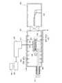
図1は、本実施の形態のレーザ照射装置の構成の一例を説明する概略図である。本実施の形態のレーザ照射装置は、レーザ光を発振するレーザ発振器301と、被照射物である基板100を載置するステージ303を有する。レーザ発振器301にはコントローラ304が接続されている。コントローラ304の制御により、レーザ発振器301から発振するレーザ光のエネルギーや、繰り返し周波数などを変化させることが可能となる。また、ステージ303は、基板100を載置する載置台307と、基板100を加熱することが可能なヒータ306と、不純物吸着材308と、が設けられており、これらがピン310によって支持台312に固定されている。FIG. 1 is a schematic diagram illustrating an example of the configuration of the laser irradiation apparatus according to the present embodiment. The laser irradiation apparatus of this embodiment includes a
レーザ発振器301とステージ303の間には、レンズやミラー等を含む光学系305が配置されている。レーザ発振器301から射出されたレーザ光は、光学系305によりそのエネルギー分布が均一化され、且つその断面形状が線状に成形される。光学系305を通過したレーザ光は、ステージ上に載置された基板100に照射される。An
なお、図示していないが、基板を載置するステージ303をチャンバー内に配置して、レーザ光を照射する工程での圧力または照射雰囲気等を制御することも可能である。この場合、レーザ発振器301及び光学系305は、チャンバー内に配置しても良いし、チャンバー外に配置し、窓を通過させてステージ上の基板100にレーザ光を照射しても良い。窓はレーザ光が通過できればよく、使用するレーザ光の強度に耐えうる耐熱性が高い材料、例えば石英板で形成することができる。Although not shown, it is also possible to place a
図2に光学系305の構成の一例を示す。図2(A)に示す光学系305はレーザビーム300の断面形状を線状に加工し、かつそのエネルギー分布を均一にするための光学系である。なお、光学系305の構成は図2の構成に限られない。FIG. 2 shows an example of the configuration of the
光学系305には、レーザ発振器301側から、シリンドリカルレンズアレイ351、シリンドリカルレンズアレイ352、シリンドリカルレンズアレイ353、シリンドリカルレンズ354、シリンドリカルレンズ355、ミラー356、ダブレットシリンドリカルレンズ357が配置されている。なお、一点鎖線で囲った領域358は光学系305の部分的な領域である。図2(B)には、光路を中心にシリンドリカルレンズアレイ351からシリンドリカルレンズ355までの各光学素子を90度回転した平面図を示している。In the
光学系305に入射したレーザ光は、シリンドリカルレンズアレイ351、シリンドリカルレンズアレイ352、シリンドリカルレンズアレイ353を通過することで、レーザ光の幅方向のエネルギープロファイルがガウシアン分布から長方形状に変化する。線状ビームは、シリンドリカルレンズ354、355を通過することで、長さ方向のビーム長が長くされ、且つ幅方向に集光される。レーザ光はミラー356で反射される。ダブレットシリンドリカルレンズ357により、レーザ光はビームの幅方向に集光される。その結果、線状のレーザ光が基板100へ照射される。The laser light incident on the
レーザ発振器301には、連続発振レーザ、疑似連続発振レーザおよびパルス発振レーザを用いることができる。なお、基板100上に設けられた半導体膜を部分溶融させるためパルス発振レーザが好ましい。パルス発振レーザの場合は、繰り返し周波数1MHz以下、パルス幅10n秒以上500n秒以下とすることができる。代表的なパルス発振レーザは、400nm以下の波長のビームを発振するエキシマレーザである。例えば、繰り返し周波数10Hz〜300Hz、パルス幅25n秒、波長308nmのXeClエキシマレーザを用いることができる。As the
レーザ光の波長は、半導体膜101に吸収される波長であり、レーザ光の表皮深さ(skin depth)等を考慮して決定することができる。例えば、波長は250nm以上700nm以下の範囲とすることができる。また、レーザ光のエネルギーも、レーザ光の波長、レーザ光の表皮深さ、半導体膜101の膜厚等を考慮して決定することができる。レーザ光のエネルギーは、例えば、300mJ/cm2以上800mJ/cm2以下の範囲とすることができる。またレーザ光の照射は、大気雰囲気のような酸素を含む雰囲気、または窒素雰囲気のような不活性雰囲気で行うことができる。窒素などの不活性雰囲気のほうが、大気雰囲気よりも半導体膜101の平坦性を向上させる効果が高く、またクラックの発生を抑える効果が高い。The wavelength of the laser light is a wavelength absorbed by the
次に、図1のレーザ照射装置によって、基板100に設けられた半導体膜にレーザ光を照射する方法を説明する。Next, a method of irradiating a semiconductor film provided on the
まず、半導体膜101を有する基板100を載置台307上に配置する。載置台307上の基板100は、載置台307下方に設けられたヒータ306によって加熱される。First, the
レーザ発振器301から射出されたレーザ光は、光学系305により断面が線状の線状ビームに形成される。図1では、紙面に垂直な方向が線状のレーザ光の長軸方向である。Laser light emitted from the
線状に加工されたレーザ光は、基板100に照射され、基板100に設けられた半導体膜101を溶融する。そして、図1の白抜き矢印に沿って、ステージ303またはレーザ光を走査しながら、且つ、ヒータ306によって基板100を加熱しながら、レーザ光を半導体膜101に照射する。図1において、白抜き矢印の方向は、線状のレーザ光の短軸方向に相当する。The laser light processed into a linear shape is applied to the
半導体膜101にレーザ光を照射することにより、半導体膜101を溶融させることができる。半導体膜101は、レーザ光によって溶融させた部分が冷却し、固化するため、平坦性が向上される。また、レーザ光の照射により平坦性の向上と共に、半導体膜の結晶欠陥が減少し、半導体膜101の結晶性を向上させることができる。By irradiating the
なお、レーザ光の照射による半導体膜101の溶融は部分溶融とすることが好ましい。完全溶融させた場合には、液相となった後の無秩序な核発生により微結晶化し、結晶性が低下する可能性が高いためである。一方で、部分溶融させることにより、溶融されていない固相部分から結晶成長が進行する。これにより、半導体膜中の結晶欠陥を減少させることができる。ここで、完全溶融とは、半導体膜101が下部界面付近まで溶融されて、液体状態になることをいう。他方、部分溶融とは、この場合、半導体膜101の上部は溶融して液相となるが、下部は溶融せずに固相のままであることをいう。Note that the melting of the
また、本実施の形態で示すレーザ照射装置は、ステージ303に設けられたヒータ306により、基板100を加熱しながら、レーザ光を照射することが可能である。これによって、溶融した半導体膜101が冷却される速度を遅くする(すなわち、半導体膜101が溶融している時間を延長する)ことができる。半導体膜101の溶融時間を溶融している時間を延長することにより、シリコン原子の移動の制限が小さくなる。溶融時、表面張力が原子の移動に作用するが、溶融時間の延長により被照射面の平坦性が格段に向上する。また、半導体膜中のダングリングボンドや、半導体膜と下地膜との界面の欠陥などのミクロな欠陥を除去することができ、より高品質の半導体膜を得ることができる。なお、ヒータの加熱温度は200℃〜1200℃程度が好ましい。適切な温度は、下地の支持基板の耐熱性や、スループットを鑑みて決定すればよい。In addition, the laser irradiation apparatus described in this embodiment can irradiate laser light while heating the
また、溶融している時間を延長することにより、半導体膜がレーザビームの照射によって溶融してから固化するまでに、次のレーザビームを照射できるため、ショット数を低減することができる。別言すると、ショット数を低減しても十分な表面の平坦性が得られる。また、ショット数を低減することは生産性の向上に寄与する。レーザビームの走査において、1回のショットと次のショットとを一部重ねてオーバーラップさせる割合をオーバーラップ率と呼ぶが、溶融している時間を延長することにより、オーバーラップ率も十分の一程度にまで低減でき、さらに0%とすることもできる。Further, by extending the melting time, the next laser beam can be irradiated from the time when the semiconductor film is melted by laser beam irradiation until it is solidified, so that the number of shots can be reduced. In other words, sufficient surface flatness can be obtained even if the number of shots is reduced. Further, reducing the number of shots contributes to improvement of productivity. In the scanning of the laser beam, the ratio of overlapping one shot and the next shot by overlapping each other is called the overlap ratio. By extending the melting time, the overlap ratio is one tenth. It can be reduced to the extent that it can be further reduced to 0%.
不純物吸着材308は、半導体膜101へ不純物が混入するのを抑制するための汚染物除去機構として設けられている。具体的には、不純物吸着材308として、例えば、シリコン基板を用いることができる。ヒータ306による加熱時に、当該ヒータから排出される炭素化合物等の不純物を不純物吸着材308によってゲッタリングすることで、レーザ光によって溶融した半導体膜101と接触しないように除去する。これによって、結晶化された半導体膜の結晶性が不純物によって低下するのを抑制することができる。The
不純物吸着材308として、シリコン基板を用いる場合には、シリコン純度が98%乃至99%の低純度シリコン(いわゆる金属シリコン)からなる基板、またはシリコン純度が11N(イレブンナイン)以上の半導体グレードの単結晶シリコン基板の双方を用いることができる。ただし、レーザ照射装置の作製コストを低減するために、金属シリコンからなる基板を用いるのが好ましい。または、シリコン基板に代えて、ガラス基板、セラミック基板、石英基板、サファイア基板などの絶縁体でなる基板、金属やステンレスなどの導電体でなる基板等の支持基板の表面を覆うように厚み100〜20000μm程度のシリコン層を設けた基板を用いてもよい。また、不純物吸着材308の形状は、板状に限られるものではなく、例えば、ヒータの周囲を囲むように加工することも可能である。When a silicon substrate is used as the
ヒータ306としては、室温から1200℃程度まで加熱が可能なヒータを用いるのが好ましい。なお、ヒータとしてグラファイトヒータを用いると、電気抵抗が温度によって大きく変化しないため、ヒータパワーがコントロールしやすく、また、形状成形も容易であるため、ヒータプロファイルの調整も容易であるため、グラファイトヒータを用いるのが好ましい。さらに、グラファイトヒータは、W(タングステン)ヒータのように再結晶化してヒータ特性が劣化することがなく、高温において機械的にも安定している。As the
しかしながら、ヒータとしてグラファイトヒータを用いた場合、加熱時にグラファイト材から一酸化炭素または二酸化炭素等の発生ガスが排気される。また、グラファイトヒータの表面コーティングに炭化珪素が用いられている場合、加熱時に炭化珪素から炭素化合物が排出されることがある。レーザ光照射により溶融した半導体膜にこれらの炭酸ガス、または炭素化合物等が付着すると、溶融した膜中に不純物として取り込まれ、半導体膜が炭素汚染されるため、半導体膜の結晶性が低下してしまう。However, when a graphite heater is used as the heater, generated gas such as carbon monoxide or carbon dioxide is exhausted from the graphite material during heating. Further, when silicon carbide is used for the surface coating of the graphite heater, the carbon compound may be discharged from the silicon carbide during heating. If these carbon dioxide gas or carbon compound adheres to the molten semiconductor film by laser light irradiation, it is taken in as an impurity in the molten film, and the semiconductor film is contaminated with carbon, so that the crystallinity of the semiconductor film is lowered. End up.
本実施の形態で示すレーザ照射装置は、ヒータ306と基板100との間に不純物吸着材308としてシリコン基板を有している。このシリコン基板によって、ヒータから発生した炭素化合物等の不純物をゲッタリングすることができる。よって、レーザ光照射による半導体膜の溶融と、ヒータによる基板の加熱を同時に行った場合にも、ヒータから発生した不純物による半導体膜の汚染を防止することができる。また、ヒータ306としてグラファイトヒータを好適に用いることが可能である。The laser irradiation apparatus described in this embodiment includes a silicon substrate as the
なお、ヒータから排出される不純物を効率よく除去するために、ヒータと対向する不純物吸着材の面積は、ヒータの上面積(不純物吸着材と対向する面積)よりも大きいことが好ましい。また、ヒータと不純物吸着材とは、近接させるのが好ましく、その距離を1mm以上10mm以下程度とするのが好ましい。In order to efficiently remove impurities discharged from the heater, the area of the impurity adsorbent facing the heater is preferably larger than the upper area of the heater (area facing the impurity adsorbent). The heater and the impurity adsorbing material are preferably close to each other, and the distance is preferably about 1 mm to 10 mm.
以上示したように、本実施の形態で示すレーザ照射装置は、半導体膜へのレーザ光照射処理において、半導体膜の不純物汚染を抑制しながら、半導体膜の溶融時間を延長することが可能である。よって、本実施の形態で示すレーザ照射装置を用いることで、結晶性および平坦性の良好な半導体膜を形成することができる。As described above, the laser irradiation apparatus described in this embodiment can extend the melting time of a semiconductor film while suppressing impurity contamination of the semiconductor film in laser light irradiation processing on the semiconductor film. . Therefore, by using the laser irradiation apparatus described in this embodiment, a semiconductor film with favorable crystallinity and flatness can be formed.
(実施の形態2)
本実施の形態では、図1に示したレーザ照射装置の構成の一例とは異なる例を図3に示す。(Embodiment 2)
In this embodiment mode, an example different from the configuration example of the laser irradiation apparatus shown in FIG. 1 is shown in FIG.
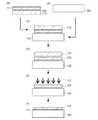
図3に示す本実施の形態のレーザ照射装置は、レーザ光を発振するレーザ発振器301と、レーザ処理チャンバー401と、レーザ処理チャンバー401に基板を搬送するための搬送チャンバー403とを有している。The laser irradiation apparatus of this embodiment mode illustrated in FIG. 3 includes a
なお、実施の形態1と同様にレーザ発振器301にはコントローラ304が接続されている。また、レーザ発振器301から射出されたレーザ光は、光学系305によりそのエネルギー分布が均一化され、且つその断面形状が線状に成形される。As in the first embodiment, a
レーザ処理チャンバー401は、ステージ303を有する。ステージ303は、基板100を載置する載置台307と、基板100を加熱することが可能なヒータ306と、が設けられており、これらがピン310によって支持台312に固定されている。図2において、ステージ303は伸縮管409と接続され、伸縮管409を用いて白抜き矢印方向に走査される。また、伸縮管409はモータ411によって制御されている。The
また、レーザ処理チャンバー401上面には、給気口405a及び給気ダクト405bを有する給気経路405が、下面には排気口407a及び排気ダクト407bを有する排気経路407がそれぞれ設けられている。給気口405a及び排気口407aは、それぞれ複数設けられているのが好ましい。給気経路405を用いてレーザ処理チャンバー401内に気体を供給し、排気経路407を用いてレーザ処理チャンバー401から気体を排出することで、レーザ処理チャンバー内の気流を下降流(ダウンフロー)に制御することが可能である。なお、排気経路407は図示しない真空ポンプに接続されていることが好ましく、真空ポンプを用いることで、レーザ処理チャンバー401内の圧力を制御することができる。Further, an
次に、図2のレーザ照射装置によって、基板100に設けられた半導体膜101にレーザ光を照射する方法を説明する。Next, a method for irradiating the
まず、搬送ロボット413を用いて半導体膜101を有する基板100を搬送チャンバー403からレーザ処理チャンバー401内に搬送し、載置台307上に配置する。載置台307上の基板100は、載置台307下方に設けられたヒータ306によって加熱される。First, the
レーザ処理チャンバー401には、給気口405aから窒素、アルゴン等の不活性ガス、または空気が給気ダクト405bを通して供給される。給気口405aから供給された気体は、レーザ処理チャンバー401内を下降流で流れ、排気口407a及び排気ダクト407bを通じてレーザ処理チャンバー401外へと排出される。また、上面(天井)に給気口405aを、下面(床面)に排気口407aをそれぞれ複数設けることで、レーザ処理チャンバー401内の気流を、被照射物である基板100表面と垂直または概略垂直な方向の層流である下降流に精度良く制御することができる。従って、レーザ処理チャンバー401内に浮遊しているパーティクル(不純物)を半導体膜101の表面に付着させることなく下降流に乗せてレーザ処理チャンバーの下部へ誘導することができる。An inert gas such as nitrogen or argon, or air is supplied to the
なお、排気経路407を通じて排出された気体は、給気経路405へと循環させることも可能である。また、レーザ処理チャンバー401の天井にHEPA(High Efficiency Particulate Air)フィルタ、ULPA(Ultra Low Penetration Air)フィルタ等の高性能フィルタを配置し、給気口405aから高性能フィルタを通じてレーザ処理チャンバー401内に清浄化された気体を供給しても良い。Note that the gas discharged through the
なお、窒素などの不活性雰囲気でレーザ光照射処理を行うほうが、大気雰囲気よりも半導体膜の平坦性を向上させる効果は高い。また、大気雰囲気よりも不活性雰囲気のほうがクラックやリッジの発生を抑える効果が高く、レーザ光の使用可能なエネルギー密度の範囲が広くなる。なお、レーザ光の照射は、減圧雰囲気で行ってもよい。減圧雰囲気でレーザ光を照射する場合には、不活性雰囲気における照射と同等の効果を得ることができる。なお、下降流による汚染防止効果を得るために、レーザ処理チャンバー401内を減圧雰囲気とする場合には、分子流領域に達しない程度、つまり、約100Pa以上とすることが
とするのが好ましい。Note that the laser light irradiation treatment in an inert atmosphere such as nitrogen has a higher effect of improving the flatness of the semiconductor film than the air atmosphere. In addition, the inert atmosphere has a higher effect of suppressing the generation of cracks and ridges than the air atmosphere, and the energy density range in which laser light can be used is widened. Note that laser light irradiation may be performed in a reduced-pressure atmosphere. When laser light is irradiated in a reduced-pressure atmosphere, the same effect as irradiation in an inert atmosphere can be obtained. In order to obtain the effect of preventing contamination due to the downflow, when the inside of the
レーザ発振器301から射出されたレーザ光は、光学系305により断面が線状の線状ビームに形成される。図1では、紙面に垂直な方向が線状のレーザ光の長軸方向である。光学系305を通過したレーザ光は、窓415を介してレーザ処理チャンバー401内に配置された基板100に照射される。なお、窓415はレーザ光が通過できればよく、使用するレーザ光の強度に耐えうる耐熱性が高い材料、例えば石英板で形成することができる。Laser light emitted from the
線状に加工されたレーザ光は、基板100に照射され、基板100に設けられた半導体膜101を溶融する。そして、図3の白抜き矢印に沿って、伸縮管409を用いてステージ303を走査しながら、且つ、ヒータ306によって基板100を加熱しながら、レーザ光を半導体膜101に照射する。図3において、白抜き矢印の方向は、線状のレーザ光の短軸方向に相当する。なお、図3では、ステージ303を走査する方法を示しているが、本実施の形態はこれに限られず、レーザ光を走査しても良い。または、レーザ光とステージ303の双方を走査しても良い。The laser light processed into a linear shape is applied to the
半導体膜101にレーザ光を照射することにより、半導体膜101を溶融させることができる。半導体膜101は、レーザ光によって溶融させた部分が冷却し、固化するため、平坦性が向上される。また、レーザ光の照射により平坦性の向上と共に、半導体膜の結晶欠陥が減少し、半導体膜101の結晶性を向上させることができる。By irradiating the
また、本実施の形態で示すレーザ照射装置は、ステージ303に設けられたヒータ306により、基板100を加熱しながら、レーザ光を照射することが可能である。これによって、溶融した半導体膜101が冷却される速度を遅くする(すなわち、半導体膜101が溶融している時間を延長する)ことができる。半導体膜101の溶融時間を溶融している時間を延長することにより、シリコン原子の移動の制限が小さくなる。溶融時、表面張力が原子の移動に作用するが、溶融時間の延長により被照射面の平坦性が格段に向上する。また、半導体膜中のダングリングボンドや、半導体膜と下地膜との界面の欠陥などのミクロな欠陥を除去することができ、より高品質の半導体膜を得ることができる。In addition, the laser irradiation apparatus described in this embodiment can irradiate laser light while heating the
さらに、本実施の形態で示すレーザ照射装置は、レーザ処理チャンバー401を有し、当該レーザ処理チャンバー401は、上面に設けられた給気経路405及び下面に設けられた排気経路407によって、気流が下降流に制御されている。従って、レーザ処理チャンバー401内に浮遊しているパーティクルを半導体膜の表面に付着させることなく下降流に乗せてレーザ処理チャンバーの下部へ誘導した後、排気経路407によってレーザ処理チャンバー401外へと排出することができる。これによって、レーザ光によって溶融した半導体膜中へ、例えばグラファイトヒータから排出される炭素化合物などの不純物が取り込まれ、半導体膜が不純物によって汚染されるのを防ぐことができる。Further, the laser irradiation apparatus described in this embodiment includes a
また、本実施の形態で示すレーザ照射装置は、レーザ処理チャンバー401の上面に設けられた給気経路405及び下面に設けられた排気経路407によって、気流が下降流に制御されている。そのため、基板表面に気体を吹き付けることで吹きつけ箇所のみ不純物の付着が防止される場合と比較して、半導体膜表面全面への不純物付着の防止効果が高い。よって、より結晶性の向上した半導体膜を作製することが可能である。なお、ステージ303に、実施の形態1で示した不純物吸着材を設けてもよい。不純物吸着材を設けることで、半導体膜中への不純物の混入をより防止することができる。In the laser irradiation apparatus described in this embodiment, the airflow is controlled to be a downward flow by an
以上示したように、本実施の形態で示すレーザ照射装置は、半導体膜へのレーザ光照射処理において、半導体膜の炭素汚染を抑制しながら、半導体膜の溶融時間を延長することが可能である。よって、本実施の形態で示すレーザ照射装置を用いることで、結晶性および平坦性の良好な半導体膜を形成することができる。As described above, the laser irradiation apparatus described in this embodiment can extend the melting time of a semiconductor film while suppressing carbon contamination of the semiconductor film in the laser irradiation process on the semiconductor film. . Therefore, by using the laser irradiation apparatus described in this embodiment, a semiconductor film with favorable crystallinity and flatness can be formed.
なお、本実施の形態は実施の形態1と組み合わせることができる。Note that this embodiment mode can be combined with Embodiment Mode 1.
(実施の形態3)
本実施の形態では、実施の形態1または2で示したレーザ照射装置を用いた半導体基板の作製方法について、図4を参照して説明する。(Embodiment 3)
In this embodiment, a method for manufacturing a semiconductor substrate using the laser irradiation apparatus described in Embodiment 1 or 2 will be described with reference to FIGS.
はじめに、基板100を用意する(図4(A)参照)。基板100には、透光性を有するガラス基板を好ましく用いることができる。ガラス基板としては、歪み点が580℃以上680℃以下(好ましくは、600℃以上680℃以下)であるものを用いると良い。また、ガラス基板は無アルカリガラス基板であることが好ましい。無アルカリガラス基板には、例えば、アルミノシリケートガラス、アルミノホウケイ酸ガラス、バリウムホウケイ酸ガラスなどのガラス材料が用いられている。First, the
なお、基板100としては、ガラス基板の他、セラミック基板、石英基板、サファイア基板などの絶縁体でなる基板、珪素などの半導体でなる基板、金属やステンレスなどの導電体でなる基板などを用いることもできる。As the
本実施の形態においては示さないが、基板100の表面に絶縁層を形成しても良い。該絶縁層を設けることにより、基板100に不純物(アルカリ金属やアルカリ土類金属など)が含まれている場合には、当該不純物が半導体層へ拡散することを防止できる。絶縁層は単層構造でも良いし積層構造でも良い。絶縁層を構成する材料としては、酸化珪素、窒化珪素、酸化窒化珪素、窒化酸化珪素などを挙げることができる。Although not shown in this embodiment mode, an insulating layer may be formed on the surface of the
次に、単結晶半導体基板110を用意する。単結晶半導体基板110としては、例えば、シリコン、ゲルマニウム、シリコンゲルマニウム、炭化シリコンなどの第4属元素でなる単結晶半導体基板を用いることができる。もちろん、ガリウムヒ素、インジウムリンなどの化合物半導体でなる基板を用いてもよい。本実施の形態においては、単結晶半導体基板110として、単結晶シリコン基板を用いることとする。単結晶半導体基板110の形状やサイズに制限は無いが、例えば、8インチ(200mm)、12インチ(300mm)、18インチ(450mm)といった円形の半導体基板を、矩形に加工して用いることができる。Next, a single
単結晶半導体基板110を洗浄した後、単結晶半導体基板110表面に絶縁層を形成する。絶縁層を設けない構成とすることもできるが、後のイオン打ち込みの際の単結晶半導体基板110の汚染及び表面の損傷を防ぐためには、絶縁層を設けることが好ましい。After the single
次に、上記絶縁層を介して、電界で加速されたイオンでなるイオンビームを単結晶半導体基板110に照射し、単結晶半導体基板110の表面から所定の深さの領域に、脆化層102を形成する。脆化層102が形成される領域の深さは、イオンビームの加速エネルギーとイオンビームの入射角によって制御することができる。ここで、脆化層102は、イオンの平均侵入深さと同程度の深さの領域に形成されることになる。Next, the single
上述の脆化層102が形成される深さにより、単結晶半導体基板110から分離される半導体層の厚さが決定される。脆化層102が形成される深さは、単結晶半導体基板110の表面から50nm以上500nm以下であり、好ましくは50nm以上200nm以下である。The thickness of the semiconductor layer separated from the single
イオンを単結晶半導体基板110に打ち込む際には、イオン注入装置又はイオンドーピング装置を用いることができる。イオン注入装置では、ソースガスを励起してイオン種を生成し、生成されたイオン種を質量分離して、所定の質量を有するイオン種を被処理物に注入する。イオンドーピング装置は、プロセスガスを励起してイオン種を生成し、生成されたイオン種を質量分離せずに被処理物に打ち込む。なお、質量分離装置を備えているイオンドーピング装置では、イオン注入装置と同様に、質量分離を伴うイオンの注入を行うこともできる。本明細書において、イオン注入装置又はイオンドーピング装置のいずれか一方を特に用いる必要がある場合にのみそれを明記し、特に明記しないときは、いずれの装置を用いてイオンの打ち込みを行っても良いこととする。When ions are implanted into the single
イオンドーピング装置を用いる場合のイオンの打ち込み工程は、例えば、以下の条件で行うことができる。
・加速電圧 10kV以上100kV以下(好ましくは30kV以上80kV以下)
・ドーズ量 1×10¹⁶ions/cm2以上4×1016ions/cm2以下
・ビーム電流密度 2μA/cm2以上(好ましくは5μA/cm2以上、より好ましくは10μA/cm2以上)The ion implantation process in the case of using an ion doping apparatus can be performed, for example, under the following conditions.
・ Acceleration voltage: 10 kV to 100 kV (preferably 30 kV to 80 kV)
・ Dose amount 1 × 10¹⁶ ions / cm2 or more and 4 × 10¹⁶ ions / cm2 or less ・ Beam current density2 μA / cm2 or more (preferably 5 μA / cm2 or more, more preferably 10 μA / cm2 or more)
イオンドーピング装置を用いる場合、イオンの打ち込み工程のソースガスには水素を含むガスを用いることができる。該ガスを用いることによりイオン種としてH+、H2+、H3+を生成することができる。該ガスをソースガスとして用いる場合には、H3+を多く打ち込むことが好ましい。具体的には、イオンビームに、H+、H2+、H3+の総量に対してH3+イオンが70%以上含まれるようにすることが好ましい。また、H3+イオンの割合を80%以上とすることがより好ましい。このようにH3+の割合を高めておくことで、脆化層102に1×10²⁰atoms/cm3以上の濃度で水素を含ませることが可能である。これにより、脆化層102からの剥離が容易になる。また、H3+イオンを多く打ち込むことで、H+、H2+を打ち込むよりもイオンの打ち込み効率が向上する。つまり、打ち込みにかかる時間を短縮することができる。In the case of using an ion doping apparatus, a gas containing hydrogen can be used as a source gas in an ion implantation process. By using the gas, H+ , H2+ , and H3+ can be generated as ionic species. When the gas is used as a source gas, it is preferable to implant a large amount of H3+ . Specifically, it is preferable that 70% or more of H3+ ions are included in the ion beam with respect to the total amount of H+ , H2+ , and H3+ . Moreover, it is more preferable that the ratio of H3+ ions is 80% or more. By increasing the ratio of H3+ in this manner, the
イオン注入装置を用いる場合には、質量分離により、H3+イオンが注入されるようにすることが好ましい。もちろん、H2+を注入してもよい。ただし、イオン注入装置を用いる場合には、イオン種を選択して注入するため、イオンドーピング装置を用いる場合と比較して、イオン打ち込みの効率が低下する場合がある。When using an ion implantation apparatus, it is preferable to implant H3+ ions by mass separation. Of course, H2+ may be implanted. However, when an ion implantation apparatus is used, since ion species are selected and implanted, the efficiency of ion implantation may be reduced as compared with the case where an ion doping apparatus is used.
上記の脆化層102を形成した後、絶縁層を除去し、新たに絶縁層111を形成する(図4(B)参照)。ここで、絶縁層を除去するのは、上記のイオン打ち込みの際に、絶縁層が損傷している可能性が高いためである。なお、絶縁層の損傷が問題とならない場合には絶縁層を除去する必要はない。After the
絶縁層111は、貼り合わせにおけるボンディング(接合)を形成する層であるから、その表面は、高い平坦性を有していることが好ましい。このような絶縁層111としては、例えば、有機シランガスを用いて化学気相成長法により形成される酸化珪素膜を用いることができる。なお、本実施の形態においては絶縁層111を単層構造としたが、2層以上の積層構造としても良い。Since the insulating
また、絶縁層111は、単結晶半導体基板110を、酸化性雰囲気下において熱処理することにより形成してもよい。熱酸化処理は、酸化性雰囲気中にハロゲンを添加した酸化を行うことが好ましい。ハロゲンを添加して熱酸化を行うことにより形成された絶縁層中にはハロゲンが含まれており、ハロゲンは1×10¹⁶atoms/cm3以上2×1021atoms/cm3以下の濃度で含まれることにより金属等の不純物を捕獲して単結晶半導体基板110の汚染を防止する保護膜としての機能を発現させることができる。The insulating
その後、上記の基板100と単結晶半導体基板110とをそれぞれ貼り合わせる(図4(C)参照)。具体的には、基板100及び絶縁層111の表面を超音波洗浄などの方法で洗浄した後、基板100の表面と絶縁層111の表面とが接触するように配置し、基板100の表面と絶縁層111の表面とでボンディング(接合)が形成されるように加圧処理を施す。ボンディングの形成には、ファン・デル・ワールス力や水素結合が関与しているものと考えられている。なお、1枚の基板上に、2枚以上の単結晶半導体基板を貼り合わせても構わない。After that, the
ボンディングを形成する前に、基板100又は絶縁層111の表面を酸素プラズマ処理又はオゾン処理して、その表面を親水性にしても良い。この処理によって、基板100又は絶縁層111の表面に水酸基が付加されるため、水素結合を効率よく形成することができる。Before forming the bonding, the surface of the
次に、貼り合わせられた基板100及び単結晶半導体基板110に対して加熱処理を施して、貼り合わせを強固なものとする。この際の加熱温度は、脆化層102における分離が進行しない温度とする必要がある。例えば、400℃未満、好ましくは300℃以下とすることができる。加熱処理時間については特に限定されず、処理速度と貼り合わせ強度との関係から最適な条件を適宜設定すればよい。本実施の形態においては、200℃、2時間の加熱処理を施すこととする。ここで、貼り合わせに係る領域のみにマイクロ波を照射して、局所的に加熱することも可能である。なお、貼り合わせ強度に問題がない場合は、上記加熱処理を省略しても良い。Next, heat treatment is performed on the bonded
次に、単結晶半導体基板110を、脆化層102にて、半導体膜101と単結晶半導体基板118とに分離する(図4(D)参照)。単結晶半導体基板110の分離は、加熱処理により行う。該加熱処理の温度は、基板100の耐熱温度を目安にすることができる。例えば、基板100としてガラス基板を用いる場合には、加熱温度は400℃以上650℃以下とすることが好ましい。ただし、短時間であれば、400℃以上700℃以下の加熱処理を行っても良い。なお、本実施の形態においては、600℃、2時間の加熱処理を施すこととする。Next, the single
上述のような加熱処理を行うことにより、脆化層102に形成された微小な空孔の体積変化が生じ、脆化層102に亀裂が生ずる。その結果、脆化層102に沿って単結晶半導体基板110が劈開する。絶縁層111は基板100と貼り合わせられているので、基板100上には単結晶半導体基板110から分離された半導体膜101が固定される。また、この加熱処理で、基板100と絶縁層111の貼り合わせに係る界面が加熱されるため、貼り合わせに係る界面に共有結合が形成され、基板100と絶縁層111の結合力が一層向上する。By performing the heat treatment as described above, a volume change of minute holes formed in the
その後、実施の形態1または2で示したレーザ照射装置を用いて、半導体膜101にレーザ光113を照射する(図4(E)参照)。実施の形態1または2のレーザ照射装置は、半導体膜へのレーザ光照射処理において、半導体膜の炭素汚染を抑制しながら、半導体膜の溶融時間を延長することが可能であり、結晶性および平坦性の良好な半導体膜を形成することができる。After that, using the laser irradiation apparatus described in Embodiment 1 or 2, the
上述のようにレーザ光113を照射した後には、半導体膜101の膜厚を小さくする薄膜化工程を行っても良い。半導体膜101の薄膜化には、ドライエッチングまたはウエットエッチングの一方、または双方を組み合わせたエッチング処理(エッチバック処理)を適用すればよい。例えば、半導体膜101がシリコン材料からなる層である場合、SF6と02をプロセスガスに用いたドライエッチング処理で、半導体膜101を薄くすることができる。After irradiation with the
なお、本実施の形態においては、レーザ光の照射により平坦化等した後でエッチング処理を行う例を挙げたが、これに限定して解釈されるものではない。例えば、レーザ光の照射前にエッチング処理を行ってもよい。この場合には、エッチング処理により半導体層表面の凹凸や欠陥をある程度低減することができる。また、レーザ光の照射前及び照射後の両方に上記処理を適用しても良い。また、レーザ光の照射と上記処理を交互に繰り返しても良い。このように、レーザ光の照射とエッチング処理を組み合わせて用いることにより、半導体層表面の凹凸、欠陥等を著しく低減することができる。もちろん、上述のエッチング処理や加熱処理などを常に用いる必要はない。Note that in this embodiment mode, an example in which an etching process is performed after planarization by laser light irradiation is given, but the present invention is not construed as being limited thereto. For example, etching treatment may be performed before laser light irradiation. In this case, the unevenness and defects on the surface of the semiconductor layer can be reduced to some extent by the etching treatment. Further, the above processing may be applied both before and after laser light irradiation. Further, the laser light irradiation and the above process may be repeated alternately. As described above, by using a combination of laser light irradiation and etching treatment, unevenness, defects, and the like on the surface of the semiconductor layer can be significantly reduced. Of course, it is not always necessary to use the above-described etching treatment or heat treatment.
以上により、表面の平坦性が向上し、欠陥が低減された半導体膜101(本実施の形態においては、単結晶シリコン半導体層)を有する半導体基板を作製することができる(図4(F)参照)。Through the above, a semiconductor substrate having the semiconductor film 101 (in this embodiment, a single crystal silicon semiconductor layer) in which surface flatness is improved and defects are reduced can be manufactured (see FIG. 4F). ).
本実施の形態は、他の実施の形態と適宜組み合わせて用いることができる。This embodiment can be combined with any of the other embodiments as appropriate.
(実施の形態4)
本実施の形態では、図5乃至7を参照して、上述の半導体基板を用いた半導体装置の作製方法について説明する。ここでは、半導体装置の一例として複数のトランジスタからなる半導体装置の作製方法について説明することとする。なお、以下において示すトランジスタを組み合わせて用いることで、様々な半導体装置を形成することができる。(Embodiment 4)
In this embodiment mode, a method for manufacturing a semiconductor device using the above-described semiconductor substrate will be described with reference to FIGS. Here, a method for manufacturing a semiconductor device including a plurality of transistors is described as an example of the semiconductor device. Note that various semiconductor devices can be formed by using a combination of the transistors described below.
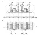
図5(A)は、実施の形態3により作製した半導体基板の断面図である。ただし、本実施の形態においては、実施の形態3における絶縁層111を2層構造とした場合について示すこととする。FIG. 5A is a cross-sectional view of the semiconductor substrate manufactured according to Embodiment 3. Note that in this embodiment, the case where the insulating
半導体膜101には、TFTのしきい値電圧を制御するために、硼素、アルミニウム、ガリウムなどのp型不純物、若しくはリン、砒素などのn型不純物を添加しても良い。不純物を添加する領域、および添加する不純物の種類は、適宜変更することができる。例えば、nチャネル型TFTの形成領域にはp型不純物を添加し、pチャネル型TFTの形成領域にn型不純物を添加することができる。上述の不純物を添加する際には、ドーズ量が1×10¹⁵ions/cm2以上1×1017ions/cm2以下程度となるように行えばよい。その後、半導体膜101を島状に分離して、半導体層702、及び半導体層704を形成する(図5(B)参照)。In order to control the threshold voltage of the TFT, a p-type impurity such as boron, aluminum, or gallium or an n-type impurity such as phosphorus or arsenic may be added to the
次に、半導体層702と半導体層704を覆うように、ゲート絶縁層706を形成する(図5(C)参照)。ここでは、プラズマCVD法を用いて、酸化珪素膜を単層で形成することとする。その他にも、酸化窒化珪素、窒化酸化珪素、窒化珪素、酸化ハフニウム、酸化アルミニウム、酸化タンタル等を含む膜を、単層構造又は積層構造で形成することによりゲート絶縁層706としても良い。Next, a
プラズマCVD法以外の作製方法としては、スパッタリング法や、高密度プラズマ処理による酸化または窒化による方法が挙げられる。高密度プラズマ処理は、例えば、ヘリウム、アルゴン、クリプトン、キセノンなどの希ガスと、酸素、酸化窒素、アンモニア、窒素、水素などガスの混合ガスを用いて行う。この場合、プラズマの励起をマイクロ波の導入により行うことで、低電子温度で高密度のプラズマを生成することができる。このような高密度のプラズマで生成された酸素ラジカル(OHラジカルを含む場合もある)や窒素ラジカル(NHラジカルを含む場合もある)によって、半導体層の表面を酸化または窒化することにより、1nm以上20nm以下、望ましくは2nm以上10nm以下の絶縁層を半導体層に接するように形成する。As a manufacturing method other than the plasma CVD method, a sputtering method or a method using oxidation or nitridation by high-density plasma treatment can be given. The high-density plasma treatment is performed using a mixed gas of a rare gas such as helium, argon, krypton, or xenon and a gas such as oxygen, nitrogen oxide, ammonia, nitrogen, or hydrogen. In this case, high-density plasma can be generated at a low electron temperature by exciting the plasma by introducing a microwave. By oxidizing or nitriding the surface of the semiconductor layer with oxygen radicals (which may include OH radicals) or nitrogen radicals (which may include NH radicals) generated by such high-density plasma, 1 nm or more An insulating layer of 20 nm or less, preferably 2 nm or more and 10 nm or less is formed so as to be in contact with the semiconductor layer.
上述した高密度プラズマ処理による半導体層の酸化または窒化は固相反応であるため、ゲート絶縁層706と半導体層702及び半導体層704との界面準位密度をきわめて低くすることができる。また、高密度プラズマ処理により半導体層を直接酸化または窒化することで、形成される絶縁層の厚さのばらつきを抑えることが出来る。また、半導体層が結晶性を有するため、高密度プラズマ処理を用いて半導体層の表面を固相反応で酸化させる場合であっても、結晶粒界における不均一な酸化を抑え、均一性が良く、界面準位密度の低いゲート絶縁層を形成することができる。このように、高密度プラズマ処理により形成された絶縁層をトランジスタのゲート絶縁層の一部または全部に用いることで、特性のばらつきを抑制することができる。Since the oxidation or nitridation of the semiconductor layer by the high-density plasma treatment described above is a solid-phase reaction, the interface state density between the
プラズマ処理による絶縁層の作製方法のより具体的な一例について説明する。亜酸化窒素(N2O)を、アルゴン(Ar)を用いて1倍以上3倍以下(流量比)に希釈し、10Pa以上30Pa以下の圧力下で3kW以上5kW以下のマイクロ波(2.45GHz)電力を印加して、半導体層702と半導体層704の表面を酸化または窒化させる。この処理により1nm以上10nm以下(好ましくは2nm以上6nm以下)のゲート絶縁層706の下層を形成する。さらに、亜酸化窒素(N2O)とシラン(SiH4)を導入し、10Pa以上30Pa以下の圧力下で3kW以上5kW以下のマイクロ波(2.45GHz)電力を印加して気相成長法により酸化窒化シリコン膜を形成し、ゲート絶縁層706の上層とする。このように、固相反応と気相成長法を組み合わせてゲート絶縁層706を形成することにより界面準位密度が低く絶縁耐圧の優れたゲート絶縁層706を形成することができる。なお、この場合においてゲート絶縁層706は2層構造となる。A more specific example of a method for manufacturing an insulating layer by plasma treatment will be described. Nitrous oxide (N2 O) is diluted 1 to 3 times (flow rate ratio) with argon (Ar), and a microwave (2.45 GHz) of 3 kW to 5 kW under a pressure of 10 Pa to 30 Pa. ) Electric power is applied to oxidize or nitride the surfaces of the
或いは、半導体層702と半導体層704を熱酸化させることで、ゲート絶縁層706を形成するようにしても良い。このような熱酸化を用いる場合には、耐熱性の比較的高いベース基板を用いることが好ましい。Alternatively, the
なお、水素を含むゲート絶縁層706を形成し、その後、350℃以上450℃以下の温度による加熱処理を行うことで、ゲート絶縁層706中に含まれる水素を半導体層702及び半導体層704中に拡散させるようにしても良い。この場合、ゲート絶縁層706として、プラズマCVD法を用いた窒化シリコン又は窒化酸化シリコンを用いることができる。なお、プロセス温度は350℃以下とすると良い。このように、半導体層702及び半導体層704に水素を供給することで、半導体層702中、半導体層704中、ゲート絶縁層706と半導体層702の界面、及びゲート絶縁層706と半導体層704の界面における欠陥を効果的に低減することができる。Note that a
次に、ゲート絶縁層706上に導電層を形成した後、該導電層を所定の形状に加工(パターニング)することで、半導体層702と半導体層704の上方に電極708を形成する(図5(D)参照)。導電層の形成にはCVD法、スパッタリング法等を用いることができる。導電層は、タンタル(Ta)、タングステン(W)、チタン(Ti)、モリブデン(Mo)、アルミニウム(Al)、銅(Cu)、クロム(Cr)、ニオブ(Nb)等の材料を用いて形成することができる。また、上記金属を主成分とする合金材料を用いても良いし、上記金属を含む化合物を用いても良い。または、半導体に導電性を付与する不純物元素をドーピングした多結晶珪素など、半導体材料を用いて形成しても良い。Next, after a conductive layer is formed over the
本実施の形態では電極708を単層の導電層で形成しているが、本発明の半導体装置は該構成に限定されない。電極708は積層された複数の導電層で形成されていても良い。2層構造とする場合には、例えば、モリブデン膜、チタン膜、窒化チタン膜等を下層に用い、上層にはアルミニウム膜などを用いればよい。3層構造の場合には、モリブデン膜とアルミニウム膜とモリブデン膜の積層構造や、チタン膜とアルミニウム膜とチタン膜の積層構造などを採用するとよい。In this embodiment mode, the
なお、電極708を形成する際に用いるマスクは、酸化珪素や窒化酸化珪素等の材料を用いて形成してもよい。この場合、酸化珪素膜や窒化酸化珪素膜等をパターニングしてマスクを形成する工程が加わるが、レジスト材料と比較して、エッチング時におけるマスクの膜減りが少ないため、より正確な形状の電極708を形成することができる。また、マスクを用いずに、液滴吐出法を用いて選択的に電極708を形成しても良い。ここで、液滴吐出法とは、所定の組成物を含む液滴を吐出または噴出することで所定のパターンを形成する方法を意味し、インクジェット法などがその範疇に含まれる。Note that a mask used for forming the
また、ICP(Inductively Coupled Plasma:誘導結合型プラズマ)エッチング法を用い、エッチング条件(コイル型の電極層に印加される電力量、基板側の電極層に印加される電力量、基板側の電極温度等)を適宜調節し、所望のテーパー形状を有するように導電層をエッチングすることで、電極708を形成することもできる。また、テーパー形状は、マスクの形状によって制御することもできる。なお、エッチング用ガスとしては、塩素、塩化硼素、塩化珪素もしくは四塩化炭素などの塩素系ガス、四弗化炭素、弗化硫黄もしくは弗化窒素などのフッ素系ガス又は酸素などを適宜用いることができる。Further, using an ICP (Inductively Coupled Plasma) etching method, etching conditions (amount of power applied to the coil-type electrode layer, a power amount applied to the electrode layer on the substrate side, and an electrode temperature on the substrate side) Etc.) is adjusted as appropriate, and the conductive layer is etched so as to have a desired tapered shape, whereby the
次に、電極708をマスクとして、一導電型を付与する不純物元素を半導体層702、半導体層704に添加する(図6(A)参照)。本実施の形態では、半導体層702にn型を付与する不純物元素(例えばリンまたはヒ素)を、半導体層704にp型を付与する不純物元素(例えばボロン)を添加する。なお、n型を付与する不純物元素を半導体層702に添加する際には、p型の不純物が添加される半導体層704はマスク等で覆い、n型を付与する不純物元素の添加が選択的に行われるようにする。また、p型を付与する不純物元素を半導体層704に添加する際には、n型の不純物が添加される半導体層702はマスク等で覆い、p型を付与する不純物元素の添加が選択的に行われるようにする。又は、半導体層702及び半導体層704に、p型を付与する不純物元素又はn型を付与する不純物元素の一方を添加した後、一方の半導体層のみに、より高い濃度でp型を付与する不純物元素又はn型を付与する不純物元素の他方を添加するようにしても良い。上記不純物の添加により、半導体層702に不純物領域710、半導体層704に不純物領域712が形成される。Next, using the
次に、電極708の側面にサイドウォール714を形成する(図6(B)参照)。サイドウォール714は、例えば、ゲート絶縁層706及び電極708を覆うように新たに絶縁層を形成し、垂直方向を主体とした異方性エッチングにより、該絶縁層を部分的にエッチングすることで形成することができる。なお、上記の異方性エッチングにより、ゲート絶縁層706を部分的にエッチングしても良い。サイドウォール714を形成するための絶縁層としては、プラズマCVD法やスパッタリング法等により、珪素、酸化珪素、窒化珪素、酸化窒化珪素、窒化酸化珪素、有機材料などを含む膜を、単層構造又は積層構造で形成すれば良い。本実施の形態では、膜厚100nmの酸化珪素膜をプラズマCVD法によって形成する。また、エッチングガスとしては、CHF3とヘリウムの混合ガスを用いることができる。なお、サイドウォール714を形成する工程は、これらに限定されるものではない。Next, a
次に、ゲート絶縁層706、電極708及びサイドウォール714をマスクとして、半導体層702、半導体層704に一導電型を付与する不純物元素を添加する(図6(C)参照)。なお、半導体層702、半導体層704には、それぞれ先の工程で添加した不純物元素と同じ導電型の不純物元素をより高い濃度で添加する。なお、n型を付与する不純物元素を半導体層702に添加する際には、p型の不純物が添加される半導体層704はマスク等で覆い、n型を付与する不純物元素の添加が選択的に行われるようにする。また、p型を付与する不純物元素を半導体層704に添加する際には、n型の不純物が添加される半導体層702はマスク等で覆い、p型を付与する不純物元素の添加が選択的に行われるようにする。Next, an impurity element imparting one conductivity type is added to the semiconductor layers 702 and 704 using the
上記不純物元素の添加により、半導体層702に、一対の高濃度不純物領域716と、一対の低濃度不純物領域718と、チャネル形成領域720とが形成される。また、上記不純物元素の添加により、半導体層704に、一対の高濃度不純物領域722と、一対の低濃度不純物領域724と、チャネル形成領域726とが形成される。高濃度不純物領域716、高濃度不純物領域722はソース又はドレインとして機能し、低濃度不純物領域718、低濃度不純物領域724はLDD(Lightly Doped Drain)領域として機能する。By the addition of the impurity element, a pair of high-
なお、半導体層702上に形成されたサイドウォール714と、半導体層704上に形成されたサイドウォール714は、キャリアが移動する方向(いわゆるチャネル長に平行な方向)の長さが同じになるように形成しても良いが、異なるように形成しても良い。pチャネル型トランジスタとなる半導体層704上のサイドウォール714の長さは、nチャネル型トランジスタとなる半導体層702上のサイドウォール714の長さよりも大きくすると良い。なぜならば、pチャネル型トランジスタにおいてソース及びドレインを形成するために注入されるボロンは拡散しやすく、短チャネル効果を誘起しやすいためである。pチャネル型トランジスタにおいて、サイドウォール714の長さをより大きくすることで、ソース及びドレインに高濃度のボロンを添加することが可能となり、ソース及びドレインを低抵抗化することができる。Note that the
ソース及びドレインをさらに低抵抗化するために、半導体層702及び半導体層704の一部をシリサイド化したシリサイド層を形成しても良い。シリサイド化は、半導体層に金属を接触させ、加熱処理(例えば、GRTA法、LRTA法等)により、半導体層中の珪素と金属とを反応させて行う。シリサイド層としては、コバルトシリサイド又はニッケルシリサイドを用いれば良い。半導体層702や半導体層704が薄い場合には、半導体層702、半導体層704の底部までシリサイド反応を進めても良い。シリサイド化に用いることができる金属材料としては、チタン(Ti)、ニッケル(Ni)、タングステン(W)、モリブデン(Mo)、コバルト(Co)、ジルコニウム(Zr)、Hf(ハフニウム)、タンタル(Ta)、バナジウム(V)、ネオジム(Nb)、クロム(Cr)、白金(Pt)、パラジウム(Pd)等が挙げられる。また、レーザ光の照射などによってもシリサイド層を形成することができる。In order to further reduce the resistance of the source and the drain, a silicide layer in which part of the
上述の工程により、nチャネル型トランジスタ728及びpチャネル型トランジスタ730が形成される。なお、図6(C)に示す段階では、ソース電極又はドレイン電極として機能する導電層は形成されていないが、これらのソース電極又はドレイン電極として機能する導電層を含めてトランジスタと呼ぶこともある。Through the above steps, an n-
次に、nチャネル型トランジスタ728、pチャネル型トランジスタ730を覆うように絶縁層732を形成する(図6(D)参照)。絶縁層732は必ずしも設ける必要はないが、絶縁層732を形成することで、アルカリ金属やアルカリ土類金属などの不純物がnチャネル型トランジスタ728、pチャネル型トランジスタ730に侵入することを防止できる。具体的には、絶縁層732を、酸化珪素、窒化珪素、酸化窒化珪素、窒化酸化珪素、窒化アルミニウム、酸化アルミニウムなどの材料を用いて形成するのが望ましい。本実施の形態では、膜厚600nm程度の窒化酸化珪素膜を、絶縁層732として用いる。この場合、上述の水素化の工程は、該窒化酸化珪素膜形成後に行っても良い。なお、本実施の形態においては、絶縁層732を単層構造としているが、積層構造としても良いことはいうまでもない。例えば、2層構造とする場合には、酸化窒化珪素膜と窒化酸化珪素膜との積層構造とすることができる。Next, an insulating
次に、nチャネル型トランジスタ728、pチャネル型トランジスタ730を覆うように、絶縁層732上に絶縁層734を形成する。絶縁層734は、ポリイミド、アクリル、ポリイミド、ベンゾシクロブテン、ポリアミド、エポキシ等の、耐熱性を有する有機材料を用いて形成するとよい。また、上記有機材料の他に、低誘電率材料(low−k材料)、シロキサン系樹脂、酸化珪素、窒化珪素、酸化窒化珪素、窒化酸化珪素、PSG(リンガラス)、BPSG(リンボロンガラス)、アルミナ等を用いることもできる。ここで、シロキサン系樹脂とは、シロキサン系材料を出発材料として形成されたSi−O−Si結合を含む樹脂に相当する。シロキサン系樹脂は、置換基に水素の他、フッ素、アルキル基、芳香族炭化水素から選ばれる一を有していても良い。なお、これらの材料で形成される絶縁層を複数積層させることで、絶縁層734を形成しても良い。Next, an insulating
絶縁層734の形成には、その材料に応じて、CVD法、スパッタ法、SOG法、スピンコート、ディップ、スプレー塗布、液滴吐出法(インクジェット法、スクリーン印刷、オフセット印刷等)、ドクターナイフ、ロールコーター、カーテンコーター、ナイフコーター等を用いることができる。For the formation of the insulating
次に、半導体層702と半導体層704の一部が露出するように絶縁層732及び絶縁層734にコンタクトホールを形成する。そして、該コンタクトホールを介して半導体層702と半導体層704に接する導電層736、導電層738を形成する(図7(A)参照)。導電層736及び導電層738は、トランジスタのソース電極又はドレイン電極として機能する。なお、本実施の形態においては、コンタクトホール開口時のエッチングに用いるガスとしてCHF3とHeの混合ガスを用いたが、これに限定されるものではない。Next, contact holes are formed in the insulating
導電層736、導電層738は、CVD法やスパッタリング法等により形成することができる。具体的には、導電層736、導電層738として、アルミニウム(Al)、タングステン(W)、チタン(Ti)、タンタル(Ta)、モリブデン(Mo)、ニッケル(Ni)、白金(Pt)、銅(Cu)、金(Au)、銀(Ag)、マンガン(Mn)、ネオジム(Nd)、炭素(C)、珪素(Si)等を用いることができる。また、上記材料を主成分とする合金を用いても良いし、上記材料を含む化合物を用いても良い。また、導電層736、導電層738は、単層構造としても良いし、積層構造としても良い。The
アルミニウムを主成分とする合金の例としては、アルミニウムを主成分として、ニッケルを含むものを挙げることができる。また、アルミニウムを主成分とし、ニッケルと、炭素または珪素の一方または両方を含むものを挙げることができる。アルミニウムやアルミニウムシリコン(Al−Si)は抵抗値が低く、安価であるため、導電層736、導電層738を形成する材料として適している。特に、アルミニウムシリコンは、パターニングの際のレジストベークによるヒロックの発生を抑制することができるため好ましい。また、珪素の代わりに、アルミニウムに0.5%程度のCuを混入させた材料を用いても良い。As an example of an alloy containing aluminum as a main component, an alloy containing aluminum as a main component and containing nickel can be given. Further, examples include aluminum as a main component and one or both of nickel and carbon or silicon. Aluminum and aluminum silicon (Al—Si) have low resistance and are inexpensive, and thus are suitable as materials for forming the
導電層736、導電層738を積層構造とする場合には、例えば、バリア膜とアルミニウムシリコン膜とバリア膜の積層構造、バリア膜とアルミニウムシリコン膜と窒化チタン膜とバリア膜の積層構造などを採用するとよい。なお、バリア膜とは、チタン、チタンの窒化物、モリブデンまたはモリブデンの窒化物などを用いて形成された膜である。バリア膜の間にアルミニウムシリコン膜を挟むように導電層を形成すると、アルミニウムやアルミニウムシリコンのヒロックの発生をより一層防止することができる。また、還元性の高い元素であるチタンを用いてバリア膜を形成すると、半導体層702と半導体層704上に薄い酸化膜が形成されていたとしても、バリア膜に含まれるチタンが該酸化膜を還元し、導電層736と半導体層702、及び導電層738と半導体層704のコンタクトを良好なものとすることができる。また、バリア膜を複数積層するようにして用いても良い。その場合、例えば、導電層736、導電層738を、下層からチタン、窒化チタン、アルミニウムシリコン、チタン、窒化チタンのように、5層構造又はそれ以上の積層構造とすることもできる。When the
また、導電層736、導電層738として、WF6ガスとSiH4ガスから化学気相成長法で形成したタングステンシリサイドを用いても良い。また、WF6を水素還元して形成したタングステンを、導電層736、導電層738として用いても良い。Alternatively, tungsten silicide formed by a chemical vapor deposition method using WF6 gas and SiH4 gas may be used for the
なお、導電層736はnチャネル型トランジスタ728の高濃度不純物領域716に接続されている。導電層738はpチャネル型トランジスタ730の高濃度不純物領域722に接続されている。Note that the
図7(B)に、図7(A)に示したnチャネル型トランジスタ728及びpチャネル型トランジスタ730の平面図を示す。ここで、図7(B)のA−Bにおける断面が図7(A)に対応している。ただし、図7(B)においては、簡単のため、導電層736、導電層738、絶縁層732、絶縁層734等を省略している。FIG. 7B is a plan view of the n-
なお、本実施の形態においては、nチャネル型トランジスタ728とpチャネル型トランジスタ730が、それぞれゲート電極として機能する電極708を1つずつ有する場合を例示しているが、本実施の形態は該構成に限定されない。本実施の形態で作製されるトランジスタは、ゲート電極として機能する電極を複数有し、なおかつ該複数の電極が電気的に接続されているマルチゲート構造を有していても良い。Note that in this embodiment, the case where each of the n-
本実施の形態では、実施の形態1または2のレーザ照射装置によって作製した結晶性および平坦性の良好な半導体基板を用いることにより、高速動作が可能で、サブスレッショルド値が低く、電界効果移動度が高く、低電圧で駆動可能なトランジスタを低いコストで作製することができる。In this embodiment mode, by using the semiconductor substrate with favorable crystallinity and flatness manufactured by the laser irradiation apparatus of Embodiment Mode 1 or 2, high-speed operation is possible, the subthreshold value is low, and the field-effect mobility is high. And a transistor that can be driven at a low voltage can be manufactured at low cost.
本実施の形態は、他の実施の形態と適宜組み合わせて用いることができる。This embodiment can be combined with any of the other embodiments as appropriate.
(実施の形態5)(Embodiment 5)
上記実施の形態で示した半導体基板を用いてトランジスタ等の半導体装置を作製し、この半導体装置を用いてさまざまな電子機器を完成することができる。実施の形態3で示した半導体基板に設けられた半導体膜は結晶欠陥が低減されているため、ゲート絶縁層との界面において、局在準位密度を低減させることが可能となる。この半導体膜を活性層として用いることで、リーク電流が低減し、電気的特性が向上した半導体素子を製造することができる。すなわち、実施の形態3で示した半導体基板を用いることで、電流駆動能力が高く、かつ信頼性の高い半導体素子を作製することが可能になり、結果として、最終製品としての電子機器をスループット良く、良好な品質で作製することが可能になる。本実施の形態では、図面を用いて具体的な電子機器への適用例を説明する。A semiconductor device such as a transistor can be manufactured using the semiconductor substrate described in any of the above embodiments, and various electronic devices can be completed using the semiconductor device. Since the semiconductor film provided on the semiconductor substrate described in Embodiment 3 has reduced crystal defects, the density of localized states can be reduced at the interface with the gate insulating layer. By using this semiconductor film as an active layer, a semiconductor element with reduced leakage current and improved electrical characteristics can be manufactured. That is, by using the semiconductor substrate described in Embodiment 3, a semiconductor element with high current driving capability and high reliability can be manufactured. As a result, an electronic device as a final product can be manufactured with high throughput. It becomes possible to produce with good quality. In this embodiment, specific application examples to electronic devices are described with reference to drawings.
半導体装置(特に表示装置)を用いて作製される電子機器としては、ビデオカメラ、デジタルカメラ、ゴーグル型ディスプレイ(ヘッドマウントディスプレイ)、ナビゲーションシステム、音響再生装置(カーオーディオコンポ等)、コンピュータ、ゲーム機器、携帯情報端末(モバイルコンピュータ、携帯電話、携帯型ゲーム機または電子書籍等)、記録媒体を備えた画像再生装置(具体的にはDigital Versatile Disc(DVD)等の記録媒体を再生し、その画像を表示しうるディスプレイを備えた装置)などが挙げられる。Electronic devices manufactured using semiconductor devices (particularly display devices) include video cameras, digital cameras, goggle-type displays (head-mounted displays), navigation systems, sound playback devices (such as car audio components), computers, and game devices. , A portable information terminal (mobile computer, cellular phone, portable game machine, electronic book, etc.), an image reproducing device (specifically, a digital versatile disc (DVD)) provided with a recording medium, and the image And the like).
図8(A)はテレビ受像器又はパーソナルコンピュータのモニタである。筺体1001、支持台1002、表示部1003、スピーカー部1004、ビデオ入力端子1005等を含む。表示部1003には、上記実施の形態で示した半導体装置が用いられており、信頼性が高く高性能なテレビ受像器又はパーソナルコンピュータのモニタを低価格で提供することができる。FIG. 8A illustrates a television receiver or a personal computer monitor. A
図8(B)はデジタルカメラである。本体1011の正面部分には受像部1013が設けられており、本体1011の上面部分にはシャッターボタン1016が設けられている。また、本体1011の背面部分には、表示部1012、操作キー1014、及び外部接続ポート1015が設けられている。表示部1012には、上記実施の形態で示した半導体装置が用いられており、信頼性が高く高性能なデジタルカメラを低価格で提供することができる。FIG. 8B illustrates a digital camera. An
図8(C)はノート型パーソナルコンピュータである。本体1021には、キーボード1024、外部接続ポート1025、ポインティングデバイス1026が設けられている。また、本体1021には、表示部1023を有する筐体1022が取り付けられている。表示部1023には、上記実施の形態で示した半導体装置が用いられており、信頼性が高く高性能なノート型パーソナルコンピュータを低価格で提供することができる。FIG. 8C illustrates a laptop personal computer. A
図8(D)はモバイルコンピュータであり、本体1031、表示部1032、スイッチ1033、操作キー1034、赤外線ポート1035等を含む。表示部1032にはアクティブマトリクス表示装置が設けられている。表示部1032には、上記実施の形態で示した半導体装置が用いられており、信頼性が高く高性能なモバイルコンピュータを低価格で提供することができる。FIG. 8D illustrates a mobile computer, which includes a
図8(E)は画像再生装置である。本体1041には、表示部B1044、記録媒体読み込み部1045及び操作キー1046が設けられている。また、本体1041には、スピーカー部1047及び表示部A1043それぞれを有する筐体1042が取り付けられている。表示部A1043及び表示部B1044それぞれには、上記実施の形態で示した半導体装置が用いられており、信頼性が高く高性能な画像再生装置を低価格で提供することができる。FIG. 8E shows an image reproducing device. The
図8(F)は電子書籍である。本体1051には操作キー1053が設けられている。また、本体1051には複数の表示部1052が取り付けられている。表示部1052には、上記実施の形態で示した半導体装置が用いられており、信頼性が高く高性能な電子書籍を低価格で提供することができる。FIG. 8F illustrates an electronic book. The
図8(G)はビデオカメラであり、本体1061には外部接続ポート1064、リモコン受信部1065、受像部1066、バッテリー1067、音声入力部1068、操作キー1069が設けられている、また、本体1061には、表示部1062を有する筐体1063が取り付けられている。表示部1062には、上記実施の形態で示した半導体装置が用いられており、信頼性が高く高性能なビデオカメラを低価格で提供することができる。FIG. 8G illustrates a video camera. A
図8(H)は携帯電話であり、本体1071、筐体1072、表示部1073、音声入力部1074、音声出力部1075、操作キー1076、外部接続ポート1077、アンテナ1078等を含む。表示部1073には、上記実施の形態で示した半導体装置が用いられており、信頼性が高く高性能な携帯電話を低価格で提供することができる。FIG. 8H illustrates a mobile phone, which includes a
図9は、電話としての機能と、情報端末としての機能を併せ持った携帯電子機器1100の構成の一例である。ここで、図9(A)は正面図、図9(B)は背面図、図9(C)は展開図である。携帯電子機器1100は、電話と情報端末の双方の機能を備えており、音声通話以外にも様々なデータ処理が可能な、いわゆるスマートフォンと呼ばれる電子機器である。FIG. 9 illustrates an example of a configuration of a portable
携帯電子機器1100は、筐体1101及び筐体1102で構成されている。筐体1101は、表示部1111、スピーカー1112、マイクロフォン1113、操作キー1114、ポインティングデバイス1115、カメラ用レンズ1116、外部接続端子1117等を備え、筐体1102は、キーボード1121、外部メモリスロット1122、カメラ用レンズ1123、ライト1124、イヤフォン端子1125等を備えている。また、アンテナは筐体1101内部に内蔵されている。上記構成に加えて、非接触ICチップ、小型記録装置等を内蔵していてもよい。A portable
表示部1111には、上記実施の形態で示した半導体装置が組み込まれている。なお、表示部1111に表示される映像(及びその表示方向)は、携帯電子機器1100の使用形態に応じて様々に変化する。また、表示部1111と同一面にカメラ用レンズ1116を備えているため、映像を伴う音声通話(いわゆるテレビ電話)が可能である。なお、スピーカー1112及びマイクロフォン1113は音声通話に限らず、録音、再生等に用いることが可能である。カメラ用レンズ1123(及び、ライト1124)を用いて静止画及び動画の撮影を行う場合には、表示部1111はファインダーとして用いられることになる。操作キー1114は、電話の発信・着信、電子メール等の簡単な情報入力、画面のスクロール、カーソル移動等に用いられる。In the
重なり合った筐体1101と筐体1102(図9(A))は、スライドし、図9(C)のように展開し、情報端末として使用できる。この場合には、キーボード1121、ポインティングデバイス1115を用いた円滑な操作が可能である。外部接続端子1117はACアダプタやUSBケーブル等の各種ケーブルと接続可能であり、充電やコンピュータ等とのデータ通信を可能にしている。また、外部メモリスロット1122に記録媒体を挿入し、より大容量のデータの保存及び移動に対応できる。上記機能に加えて、赤外線などの電磁波を用いた無線通信機能や、テレビ受信機能等を有していても良い。上記実施の形態で示した半導体装置を搭載することで、信頼性が高く高性能な携帯電子機器を低価格で提供することができる。The
以上の様に、本実施の形態の適用範囲は極めて広く、あらゆる分野の電子機器に用いることが可能である。なお、本実施の形態は、他の実施の形態と適宜組み合わせて用いることができる。As described above, the application range of this embodiment is extremely wide and can be used for electronic devices in various fields. Note that this embodiment can be combined with any of the other embodiments as appropriate.
100 基板
101 半導体膜
102 脆化層
110 単結晶半導体基板
111 絶縁層
113 レーザ光
118 単結晶半導体基板
300 レーザビーム
301 レーザ発振器
303 ステージ
304 コントローラ
305 光学系
306 ヒータ
307 載置台
308 不純物吸着材
310 ピン
312 支持台
351 シリンドリカルレンズアレイ
352 シリンドリカルレンズアレイ
353 シリンドリカルレンズアレイ
354 シリンドリカルレンズ
355 シリンドリカルレンズ
356 ミラー
357 ダブレットシリンドリカルレンズ
358 領域
401 レーザ処理チャンバー
403 搬送チャンバー
405 給気経路
405a 給気口
405b 給気ダクト
407 排気経路
407a 排気口
407b 排気ダクト
409 伸縮管
411 モータ
413 搬送ロボット
415 窓
702 半導体層
704 半導体層
706 ゲート絶縁層
708 電極
710 不純物領域
712 不純物領域
714 サイドウォール
716 高濃度不純物領域
718 低濃度不純物領域
720 チャネル形成領域
722 高濃度不純物領域
724 低濃度不純物領域
726 チャネル形成領域
728 nチャネル型トランジスタ
730 pチャネル型トランジスタ
732 絶縁層
734 絶縁層
736 導電層
738 導電層
1001 筺体
1002 支持台
1003 表示部
1004 スピーカー部
1005 ビデオ入力端子
1011 本体
1012 表示部
1013 受像部
1014 操作キー
1015 外部接続ポート
1016 シャッターボタン
1021 本体
1022 筐体
1023 表示部
1024 キーボード
1025 外部接続ポート
1026 ポインティングデバイス
1031 本体
1032 表示部
1033 スイッチ
1034 操作キー
1035 赤外線ポート
1041 本体
1042 筐体
1043 表示部A
1044 表示部B
1045 部
1046 操作キー
1047 スピーカー部
1051 本体
1052 表示部
1053 操作キー
1061 本体
1062 表示部
1063 筐体
1064 外部接続ポート
1065 リモコン受信部
1066 受像部
1067 バッテリー
1068 音声入力部
1069 操作キー
1071 本体
1072 筐体
1073 表示部
1074 音声入力部
1075 音声出力部
1076 操作キー
1077 外部接続ポート
1078 アンテナ
1100 携帯電子機器
1101 筐体
1102 筐体
1111 表示部
1112 スピーカー
1113 マイクロフォン
1114 操作キー
1115 ポインティングデバイス
1116 カメラ用レンズ
1117 外部接続端子
1121 キーボード
1122 外部メモリスロット
1123 カメラ用レンズ
1124 ライト
1125 イヤフォン端子100 substrate 101 semiconductor film 102 embrittlement layer 110 single crystal semiconductor substrate 111 insulating layer 113 laser beam 118 single crystal semiconductor substrate 300 laser beam 301 laser oscillator 303 stage 304 controller 305 optical system 306 heater 307 mounting base 308 impurity adsorbent 310 pin 312 Support base 351 Cylindrical lens array 352 Cylindrical lens array 353 Cylindrical lens array 354 Cylindrical lens 355 Cylindrical lens 356 Mirror 357 Doublet cylindrical lens 358 Area 401 Laser processing chamber 403 Transport chamber 405 Air supply path 405a Air supply port 405b Air supply duct 407 Exhaust path 407a Exhaust port 407b Exhaust duct 409 Telescopic tube 411 Motor 413 Transport robot 415 Window 702 Semiconductor layer 704 Semiconductor layer 706 Gate insulating layer 708 Electrode 710 Impurity region 712 Impurity region 714 Side wall 716 High concentration impurity region 718 Low concentration impurity region 720 Channel formation region 722 High concentration impurity region 724 Low concentration impurity region 726 Channel formation region 728 n-channel transistor 730 p-channel transistor 732 insulating layer 734 insulating layer 736 conductive layer 738 conductive layer 1001 housing 1002 support base 1003 display unit 1004 speaker unit 1005 video input terminal 1011 main body 1012 display unit 1013 image receiving unit 1014 operation key 1015 external Connection port 1016 Shutter button 1021 Main body 1022 Case 1023 Display unit 1024 Keyboard 1025 External connection port 1026 Pointing device 031 body 1032 display unit 1033 switches 1034 operation keys 1035 infrared port 1041 body 1042 housing 1043 display portion A
1044 Display unit B
1045
Claims (8)
Translated fromJapanese前記レーザ発振器から射出されたレーザ光を線状に成形する光学系と、
前記光学系によって成形された線状のレーザ光が照射される被照射物を載置するステージと、を有し、
前記ステージは、支持台上に、ヒータ、不純物吸着材及び前記被照射物を載置する載置台が順に固定されていることを特徴とするレーザ照射装置。A laser oscillator;
An optical system for linearly shaping laser light emitted from the laser oscillator;
A stage on which an object to be irradiated with linear laser light molded by the optical system is placed;
The laser irradiation apparatus according to claim 1, wherein the stage has a mounting table on which a heater, an impurity adsorbent, and the irradiation object are mounted in order on a support table.
前記レーザ発振器から射出されたレーザ光を線状に成形する光学系と、
上面に給気経路が、下面に排気経路がそれぞれ設けられたレーザ処理チャンバーと、
前記レーザ処理チャンバー内に配置され、前記光学系によって成形された線状のレーザ光が照射される被照射物を載置するステージと、を有し、
前記レーザ処理チャンバー内の気流は、前記給気経路及び前記排気経路によって下降流に制御され、
前記ステージは、支持台上に、ヒータ及び前記被照射物を載置する載置台が順に固定されていることを特徴とするレーザ照射装置。A laser oscillator;
An optical system for linearly shaping laser light emitted from the laser oscillator;
A laser processing chamber having an air supply path on the upper surface and an exhaust path on the lower surface;
A stage for placing an object to be irradiated with linear laser light that is arranged in the laser processing chamber and shaped by the optical system;
The air flow in the laser processing chamber is controlled to a downward flow by the air supply path and the exhaust path,
The laser irradiation apparatus, wherein the stage has a heater and a mounting table on which the object to be irradiated is mounted in order on a support table.
前記下降流は、前記被照射物表面と垂直な方向の層流であることを特徴とするレーザ照射装置。In claim 2,
The laser irradiation apparatus according to claim 1, wherein the downward flow is a laminar flow in a direction perpendicular to the surface of the irradiation object.
前記ステージは、前記ヒータと前記載置台の間に、不純物吸着材を有することを特徴とするレーザ照射装置。In claim 2 or 3,
The laser irradiation apparatus, wherein the stage has an impurity adsorbing material between the heater and the mounting table.
前記ヒータと前記不純物吸着材との距離は、1mm以上10mm以下であることを特徴とするレーザ照射装置。In claim 1 or 4,
The laser irradiation apparatus characterized in that a distance between the heater and the impurity adsorbent is 1 mm or more and 10 mm or less.
前記不純物吸着材として、シリコン純度が98%乃至99%の低純度シリコンからなるシリコン基板を用いることを特徴とするレーザ照射装置。In any one of claims 1, 4 or 5,
A laser irradiation apparatus using a silicon substrate made of low-purity silicon having a silicon purity of 98% to 99% as the impurity adsorbing material.
前記ヒータとして、グラファイトヒータを用いることを特徴とするレーザ照射装置。In any one of Claims 1 thru | or 6,
A laser irradiation apparatus using a graphite heater as the heater.
Priority Applications (1)
| Application Number | Priority Date | Filing Date | Title |
|---|---|---|---|
| JP2009197200AJP5500914B2 (en) | 2009-08-27 | 2009-08-27 | Laser irradiation device |
Applications Claiming Priority (1)
| Application Number | Priority Date | Filing Date | Title |
|---|---|---|---|
| JP2009197200AJP5500914B2 (en) | 2009-08-27 | 2009-08-27 | Laser irradiation device |
Publications (3)
| Publication Number | Publication Date |
|---|---|
| JP2011049398Atrue JP2011049398A (en) | 2011-03-10 |
| JP2011049398A5 JP2011049398A5 (en) | 2012-08-30 |
| JP5500914B2 JP5500914B2 (en) | 2014-05-21 |
Family
ID=43835438
Family Applications (1)
| Application Number | Title | Priority Date | Filing Date |
|---|---|---|---|
| JP2009197200AExpired - Fee RelatedJP5500914B2 (en) | 2009-08-27 | 2009-08-27 | Laser irradiation device |
Country Status (1)
| Country | Link |
|---|---|
| JP (1) | JP5500914B2 (en) |
Cited By (39)
| Publication number | Priority date | Publication date | Assignee | Title |
|---|---|---|---|---|
| US9676167B2 (en) | 2013-12-17 | 2017-06-13 | Corning Incorporated | Laser processing of sapphire substrate and related applications |
| US9701563B2 (en) | 2013-12-17 | 2017-07-11 | Corning Incorporated | Laser cut composite glass article and method of cutting |
| US9815144B2 (en) | 2014-07-08 | 2017-11-14 | Corning Incorporated | Methods and apparatuses for laser processing materials |
| US9815730B2 (en) | 2013-12-17 | 2017-11-14 | Corning Incorporated | Processing 3D shaped transparent brittle substrate |
| US9850159B2 (en) | 2012-11-20 | 2017-12-26 | Corning Incorporated | High speed laser processing of transparent materials |
| US9850160B2 (en) | 2013-12-17 | 2017-12-26 | Corning Incorporated | Laser cutting of display glass compositions |
| WO2018025495A1 (en)* | 2016-08-04 | 2018-02-08 | 株式会社日本製鋼所 | Laser release device, laser release method, and method for manufacturing organic el display |
| JP2018024014A (en)* | 2016-08-04 | 2018-02-15 | 株式会社日本製鋼所 | Laser peeling apparatus, laser peeling method, and organic EL display manufacturing method |
| US10047001B2 (en) | 2014-12-04 | 2018-08-14 | Corning Incorporated | Glass cutting systems and methods using non-diffracting laser beams |
| US10144093B2 (en) | 2013-12-17 | 2018-12-04 | Corning Incorporated | Method for rapid laser drilling of holes in glass and products made therefrom |
| US10173916B2 (en) | 2013-12-17 | 2019-01-08 | Corning Incorporated | Edge chamfering by mechanically processing laser cut glass |
| US10233112B2 (en) | 2013-12-17 | 2019-03-19 | Corning Incorporated | Laser processing of slots and holes |
| US10252931B2 (en) | 2015-01-12 | 2019-04-09 | Corning Incorporated | Laser cutting of thermally tempered substrates |
| US10280108B2 (en) | 2013-03-21 | 2019-05-07 | Corning Laser Technologies GmbH | Device and method for cutting out contours from planar substrates by means of laser |
| US10335902B2 (en) | 2014-07-14 | 2019-07-02 | Corning Incorporated | Method and system for arresting crack propagation |
| US10377658B2 (en) | 2016-07-29 | 2019-08-13 | Corning Incorporated | Apparatuses and methods for laser processing |
| US10421683B2 (en) | 2013-01-15 | 2019-09-24 | Corning Laser Technologies GmbH | Method and device for the laser-based machining of sheet-like substrates |
| US10522963B2 (en) | 2016-08-30 | 2019-12-31 | Corning Incorporated | Laser cutting of materials with intensity mapping optical system |
| US10525657B2 (en) | 2015-03-27 | 2020-01-07 | Corning Incorporated | Gas permeable window and method of fabricating the same |
| US10526234B2 (en) | 2014-07-14 | 2020-01-07 | Corning Incorporated | Interface block; system for and method of cutting a substrate being transparent within a range of wavelengths using such interface block |
| US10611667B2 (en) | 2014-07-14 | 2020-04-07 | Corning Incorporated | Method and system for forming perforations |
| US10626040B2 (en) | 2017-06-15 | 2020-04-21 | Corning Incorporated | Articles capable of individual singulation |
| US10688599B2 (en) | 2017-02-09 | 2020-06-23 | Corning Incorporated | Apparatus and methods for laser processing transparent workpieces using phase shifted focal lines |
| US10730783B2 (en) | 2016-09-30 | 2020-08-04 | Corning Incorporated | Apparatuses and methods for laser processing transparent workpieces using non-axisymmetric beam spots |
| US10752534B2 (en) | 2016-11-01 | 2020-08-25 | Corning Incorporated | Apparatuses and methods for laser processing laminate workpiece stacks |
| JP2021042472A (en)* | 2019-09-09 | 2021-03-18 | シュトゥルム マシーネン ウント アラゲンバウ ゲゼルシャフト ミット ベシュレンクテル ハフツングSturm Maschinen− & Anlagenbau GmbH | Coating device and method for subjecting workpiece to metal coating |
| US11062986B2 (en) | 2017-05-25 | 2021-07-13 | Corning Incorporated | Articles having vias with geometry attributes and methods for fabricating the same |
| US11078112B2 (en) | 2017-05-25 | 2021-08-03 | Corning Incorporated | Silica-containing substrates with vias having an axially variable sidewall taper and methods for forming the same |
| US11114309B2 (en) | 2016-06-01 | 2021-09-07 | Corning Incorporated | Articles and methods of forming vias in substrates |
| US11111170B2 (en) | 2016-05-06 | 2021-09-07 | Corning Incorporated | Laser cutting and removal of contoured shapes from transparent substrates |
| US11186060B2 (en) | 2015-07-10 | 2021-11-30 | Corning Incorporated | Methods of continuous fabrication of holes in flexible substrate sheets and products relating to the same |
| US11542190B2 (en) | 2016-10-24 | 2023-01-03 | Corning Incorporated | Substrate processing station for laser-based machining of sheet-like glass substrates |
| US11554984B2 (en) | 2018-02-22 | 2023-01-17 | Corning Incorporated | Alkali-free borosilicate glasses with low post-HF etch roughness |
| US11556039B2 (en) | 2013-12-17 | 2023-01-17 | Corning Incorporated | Electrochromic coated glass articles and methods for laser processing the same |
| US11648623B2 (en) | 2014-07-14 | 2023-05-16 | Corning Incorporated | Systems and methods for processing transparent materials using adjustable laser beam focal lines |
| JP2023077014A (en)* | 2021-11-24 | 2023-06-05 | 株式会社ディスコ | Generation method of wafer |
| US11774233B2 (en) | 2016-06-29 | 2023-10-03 | Corning Incorporated | Method and system for measuring geometric parameters of through holes |
| US11773004B2 (en) | 2015-03-24 | 2023-10-03 | Corning Incorporated | Laser cutting and processing of display glass compositions |
| US12180108B2 (en) | 2017-12-19 | 2024-12-31 | Corning Incorporated | Methods for etching vias in glass-based articles employing positive charge organic molecules |
Families Citing this family (1)
| Publication number | Priority date | Publication date | Assignee | Title |
|---|---|---|---|---|
| DE102017129479A1 (en)* | 2017-12-11 | 2019-06-13 | Trumpf Laser- Und Systemtechnik Gmbh | Laser processing device for processing workpieces by means of a laser |
Citations (9)
| Publication number | Priority date | Publication date | Assignee | Title |
|---|---|---|---|---|
| JPH06295859A (en)* | 1992-11-06 | 1994-10-21 | Semiconductor Energy Lab Co Ltd | Laser treating method |
| JPH08191049A (en)* | 1995-01-11 | 1996-07-23 | Hitachi Ltd | Semiconductor manufacturing equipment |
| JPH11111628A (en)* | 1997-09-30 | 1999-04-23 | Shin Etsu Chem Co Ltd | Silicon heating element and semiconductor manufacturing apparatus using the same |
| JP2000012549A (en)* | 1998-06-17 | 2000-01-14 | Sukegawa Electric Co Ltd | Plate heating apparatus |
| JP2004039953A (en)* | 2002-07-05 | 2004-02-05 | Renesas Technology Corp | Manufacturing method of semiconductor device |
| JP2004172610A (en)* | 2002-11-08 | 2004-06-17 | Semiconductor Energy Lab Co Ltd | Method for producing semiconductor device, semiconductor device, and laser irradiation apparatus |
| JP2004304096A (en)* | 2003-04-01 | 2004-10-28 | Tokyo Electron Ltd | Heat-treatment method and apparatus |
| WO2004114377A1 (en)* | 2003-06-23 | 2004-12-29 | Tokyo Electron Limited | Heat treatment apparatus |
| JP2008243820A (en)* | 1997-07-31 | 2008-10-09 | Covalent Materials Corp | Carbon heater |
- 2009
- 2009-08-27JPJP2009197200Apatent/JP5500914B2/ennot_activeExpired - Fee Related
Patent Citations (9)
| Publication number | Priority date | Publication date | Assignee | Title |
|---|---|---|---|---|
| JPH06295859A (en)* | 1992-11-06 | 1994-10-21 | Semiconductor Energy Lab Co Ltd | Laser treating method |
| JPH08191049A (en)* | 1995-01-11 | 1996-07-23 | Hitachi Ltd | Semiconductor manufacturing equipment |
| JP2008243820A (en)* | 1997-07-31 | 2008-10-09 | Covalent Materials Corp | Carbon heater |
| JPH11111628A (en)* | 1997-09-30 | 1999-04-23 | Shin Etsu Chem Co Ltd | Silicon heating element and semiconductor manufacturing apparatus using the same |
| JP2000012549A (en)* | 1998-06-17 | 2000-01-14 | Sukegawa Electric Co Ltd | Plate heating apparatus |
| JP2004039953A (en)* | 2002-07-05 | 2004-02-05 | Renesas Technology Corp | Manufacturing method of semiconductor device |
| JP2004172610A (en)* | 2002-11-08 | 2004-06-17 | Semiconductor Energy Lab Co Ltd | Method for producing semiconductor device, semiconductor device, and laser irradiation apparatus |
| JP2004304096A (en)* | 2003-04-01 | 2004-10-28 | Tokyo Electron Ltd | Heat-treatment method and apparatus |
| WO2004114377A1 (en)* | 2003-06-23 | 2004-12-29 | Tokyo Electron Limited | Heat treatment apparatus |
Cited By (57)
| Publication number | Priority date | Publication date | Assignee | Title |
|---|---|---|---|---|
| US9850159B2 (en) | 2012-11-20 | 2017-12-26 | Corning Incorporated | High speed laser processing of transparent materials |
| US11028003B2 (en) | 2013-01-15 | 2021-06-08 | Corning Laser Technologies GmbH | Method and device for laser-based machining of flat substrates |
| US10421683B2 (en) | 2013-01-15 | 2019-09-24 | Corning Laser Technologies GmbH | Method and device for the laser-based machining of sheet-like substrates |
| US11345625B2 (en) | 2013-01-15 | 2022-05-31 | Corning Laser Technologies GmbH | Method and device for the laser-based machining of sheet-like substrates |
| US11713271B2 (en) | 2013-03-21 | 2023-08-01 | Corning Laser Technologies GmbH | Device and method for cutting out contours from planar substrates by means of laser |
| US10280108B2 (en) | 2013-03-21 | 2019-05-07 | Corning Laser Technologies GmbH | Device and method for cutting out contours from planar substrates by means of laser |
| US10183885B2 (en) | 2013-12-17 | 2019-01-22 | Corning Incorporated | Laser cut composite glass article and method of cutting |
| US9815730B2 (en) | 2013-12-17 | 2017-11-14 | Corning Incorporated | Processing 3D shaped transparent brittle substrate |
| US9676167B2 (en) | 2013-12-17 | 2017-06-13 | Corning Incorporated | Laser processing of sapphire substrate and related applications |
| US10144093B2 (en) | 2013-12-17 | 2018-12-04 | Corning Incorporated | Method for rapid laser drilling of holes in glass and products made therefrom |
| US10173916B2 (en) | 2013-12-17 | 2019-01-08 | Corning Incorporated | Edge chamfering by mechanically processing laser cut glass |
| US10179748B2 (en) | 2013-12-17 | 2019-01-15 | Corning Incorporated | Laser processing of sapphire substrate and related applications |
| US10597321B2 (en) | 2013-12-17 | 2020-03-24 | Corning Incorporated | Edge chamfering methods |
| US10233112B2 (en) | 2013-12-17 | 2019-03-19 | Corning Incorporated | Laser processing of slots and holes |
| US9850160B2 (en) | 2013-12-17 | 2017-12-26 | Corning Incorporated | Laser cutting of display glass compositions |
| US11148225B2 (en) | 2013-12-17 | 2021-10-19 | Corning Incorporated | Method for rapid laser drilling of holes in glass and products made therefrom |
| US10293436B2 (en) | 2013-12-17 | 2019-05-21 | Corning Incorporated | Method for rapid laser drilling of holes in glass and products made therefrom |
| US11556039B2 (en) | 2013-12-17 | 2023-01-17 | Corning Incorporated | Electrochromic coated glass articles and methods for laser processing the same |
| US10611668B2 (en) | 2013-12-17 | 2020-04-07 | Corning Incorporated | Laser cut composite glass article and method of cutting |
| US10392290B2 (en) | 2013-12-17 | 2019-08-27 | Corning Incorporated | Processing 3D shaped transparent brittle substrate |
| US9701563B2 (en) | 2013-12-17 | 2017-07-11 | Corning Incorporated | Laser cut composite glass article and method of cutting |
| US10442719B2 (en) | 2013-12-17 | 2019-10-15 | Corning Incorporated | Edge chamfering methods |
| US9815144B2 (en) | 2014-07-08 | 2017-11-14 | Corning Incorporated | Methods and apparatuses for laser processing materials |
| US11697178B2 (en) | 2014-07-08 | 2023-07-11 | Corning Incorporated | Methods and apparatuses for laser processing materials |
| US10611667B2 (en) | 2014-07-14 | 2020-04-07 | Corning Incorporated | Method and system for forming perforations |
| US11648623B2 (en) | 2014-07-14 | 2023-05-16 | Corning Incorporated | Systems and methods for processing transparent materials using adjustable laser beam focal lines |
| US10335902B2 (en) | 2014-07-14 | 2019-07-02 | Corning Incorporated | Method and system for arresting crack propagation |
| US10526234B2 (en) | 2014-07-14 | 2020-01-07 | Corning Incorporated | Interface block; system for and method of cutting a substrate being transparent within a range of wavelengths using such interface block |
| US10047001B2 (en) | 2014-12-04 | 2018-08-14 | Corning Incorporated | Glass cutting systems and methods using non-diffracting laser beams |
| US11014845B2 (en) | 2014-12-04 | 2021-05-25 | Corning Incorporated | Method of laser cutting glass using non-diffracting laser beams |
| US10252931B2 (en) | 2015-01-12 | 2019-04-09 | Corning Incorporated | Laser cutting of thermally tempered substrates |
| US11773004B2 (en) | 2015-03-24 | 2023-10-03 | Corning Incorporated | Laser cutting and processing of display glass compositions |
| US10525657B2 (en) | 2015-03-27 | 2020-01-07 | Corning Incorporated | Gas permeable window and method of fabricating the same |
| US11186060B2 (en) | 2015-07-10 | 2021-11-30 | Corning Incorporated | Methods of continuous fabrication of holes in flexible substrate sheets and products relating to the same |
| US11111170B2 (en) | 2016-05-06 | 2021-09-07 | Corning Incorporated | Laser cutting and removal of contoured shapes from transparent substrates |
| US11114309B2 (en) | 2016-06-01 | 2021-09-07 | Corning Incorporated | Articles and methods of forming vias in substrates |
| US11774233B2 (en) | 2016-06-29 | 2023-10-03 | Corning Incorporated | Method and system for measuring geometric parameters of through holes |
| US10377658B2 (en) | 2016-07-29 | 2019-08-13 | Corning Incorporated | Apparatuses and methods for laser processing |
| JP6999264B2 (en) | 2016-08-04 | 2022-01-18 | 株式会社日本製鋼所 | Laser peeling device, laser peeling method, and manufacturing method of organic EL display |
| US11471974B2 (en) | 2016-08-04 | 2022-10-18 | Jsw Aktina System Co., Ltd. | Laser lift-off apparatus, laser lift-off method, and method for manufacturing organic el display |
| JP2018024014A (en)* | 2016-08-04 | 2018-02-15 | 株式会社日本製鋼所 | Laser peeling apparatus, laser peeling method, and organic EL display manufacturing method |
| WO2018025495A1 (en)* | 2016-08-04 | 2018-02-08 | 株式会社日本製鋼所 | Laser release device, laser release method, and method for manufacturing organic el display |
| JP2022043196A (en)* | 2016-08-04 | 2022-03-15 | 株式会社日本製鋼所 | Laser peeling device, laser peeling method, and manufacturing method of organic EL display |
| US10522963B2 (en) | 2016-08-30 | 2019-12-31 | Corning Incorporated | Laser cutting of materials with intensity mapping optical system |
| US10730783B2 (en) | 2016-09-30 | 2020-08-04 | Corning Incorporated | Apparatuses and methods for laser processing transparent workpieces using non-axisymmetric beam spots |
| US11130701B2 (en) | 2016-09-30 | 2021-09-28 | Corning Incorporated | Apparatuses and methods for laser processing transparent workpieces using non-axisymmetric beam spots |
| US11542190B2 (en) | 2016-10-24 | 2023-01-03 | Corning Incorporated | Substrate processing station for laser-based machining of sheet-like glass substrates |
| US10752534B2 (en) | 2016-11-01 | 2020-08-25 | Corning Incorporated | Apparatuses and methods for laser processing laminate workpiece stacks |
| US10688599B2 (en) | 2017-02-09 | 2020-06-23 | Corning Incorporated | Apparatus and methods for laser processing transparent workpieces using phase shifted focal lines |
| US11972993B2 (en) | 2017-05-25 | 2024-04-30 | Corning Incorporated | Silica-containing substrates with vias having an axially variable sidewall taper and methods for forming the same |
| US11062986B2 (en) | 2017-05-25 | 2021-07-13 | Corning Incorporated | Articles having vias with geometry attributes and methods for fabricating the same |
| US11078112B2 (en) | 2017-05-25 | 2021-08-03 | Corning Incorporated | Silica-containing substrates with vias having an axially variable sidewall taper and methods for forming the same |
| US10626040B2 (en) | 2017-06-15 | 2020-04-21 | Corning Incorporated | Articles capable of individual singulation |
| US12180108B2 (en) | 2017-12-19 | 2024-12-31 | Corning Incorporated | Methods for etching vias in glass-based articles employing positive charge organic molecules |
| US11554984B2 (en) | 2018-02-22 | 2023-01-17 | Corning Incorporated | Alkali-free borosilicate glasses with low post-HF etch roughness |
| JP2021042472A (en)* | 2019-09-09 | 2021-03-18 | シュトゥルム マシーネン ウント アラゲンバウ ゲゼルシャフト ミット ベシュレンクテル ハフツングSturm Maschinen− & Anlagenbau GmbH | Coating device and method for subjecting workpiece to metal coating |
| JP2023077014A (en)* | 2021-11-24 | 2023-06-05 | 株式会社ディスコ | Generation method of wafer |
Also Published As
| Publication number | Publication date |
|---|---|
| JP5500914B2 (en) | 2014-05-21 |
Similar Documents
| Publication | Publication Date | Title |
|---|---|---|
| JP5500914B2 (en) | Laser irradiation device | |
| CN101562153B (en) | Semiconductor device and method for manufacturing semiconductor device | |
| JP5404064B2 (en) | Laser processing apparatus and semiconductor substrate manufacturing method | |
| TW544938B (en) | Method of manufacturing a semiconductor device | |
| JP5586912B2 (en) | Method for manufacturing semiconductor substrate | |
| JP5433220B2 (en) | Semiconductor device and manufacturing method thereof | |
| US8492248B2 (en) | Manufacturing method of semiconductor substrate | |
| JP5586906B2 (en) | Method for manufacturing semiconductor device | |
| JP5583916B2 (en) | Method for manufacturing semiconductor substrate and method for manufacturing semiconductor device | |
| JP5925440B2 (en) | Method for manufacturing SOI substrate and method for manufacturing semiconductor device | |
| JP5284669B2 (en) | Method for manufacturing semiconductor device | |
| JP5279260B2 (en) | Semiconductor layer evaluation method | |
| JP5576617B2 (en) | Method for evaluating crystallinity of single crystal semiconductor layer | |
| US20120045883A1 (en) | Method for manufacturing soi substrate | |
| KR101641499B1 (en) | Method for manufacturing soi substrate | |
| JP2009212387A (en) | Method of manufacturing semiconductor substrate |
Legal Events
| Date | Code | Title | Description |
|---|---|---|---|
| A521 | Written amendment | Free format text:JAPANESE INTERMEDIATE CODE: A523 Effective date:20120718 | |
| A621 | Written request for application examination | Free format text:JAPANESE INTERMEDIATE CODE: A621 Effective date:20120718 | |
| A977 | Report on retrieval | Free format text:JAPANESE INTERMEDIATE CODE: A971007 Effective date:20131212 | |
| A131 | Notification of reasons for refusal | Free format text:JAPANESE INTERMEDIATE CODE: A131 Effective date:20140107 | |
| A521 | Written amendment | Free format text:JAPANESE INTERMEDIATE CODE: A523 Effective date:20140206 | |
| TRDD | Decision of grant or rejection written | ||
| A01 | Written decision to grant a patent or to grant a registration (utility model) | Free format text:JAPANESE INTERMEDIATE CODE: A01 Effective date:20140304 | |
| A61 | First payment of annual fees (during grant procedure) | Free format text:JAPANESE INTERMEDIATE CODE: A61 Effective date:20140311 | |
| R150 | Certificate of patent or registration of utility model | Ref document number:5500914 Country of ref document:JP Free format text:JAPANESE INTERMEDIATE CODE: R150 | |
| R250 | Receipt of annual fees | Free format text:JAPANESE INTERMEDIATE CODE: R250 | |
| LAPS | Cancellation because of no payment of annual fees |