JP2011049270A - Method of manufacturing semiconductor device, and semiconductor device - Google Patents
Method of manufacturing semiconductor device, and semiconductor deviceDownload PDFInfo
- Publication number
- JP2011049270A JP2011049270AJP2009195112AJP2009195112AJP2011049270AJP 2011049270 AJP2011049270 AJP 2011049270AJP 2009195112 AJP2009195112 AJP 2009195112AJP 2009195112 AJP2009195112 AJP 2009195112AJP 2011049270 AJP2011049270 AJP 2011049270A
- Authority
- JP
- Japan
- Prior art keywords
- metal electrode
- interlayer insulating
- insulating film
- opening
- substrate
- Prior art date
- Legal status (The legal status is an assumption and is not a legal conclusion. Google has not performed a legal analysis and makes no representation as to the accuracy of the status listed.)
- Granted
Links
Images


Classifications
- H—ELECTRICITY
- H01—ELECTRIC ELEMENTS
- H01L—SEMICONDUCTOR DEVICES NOT COVERED BY CLASS H10
- H01L2224/00—Indexing scheme for arrangements for connecting or disconnecting semiconductor or solid-state bodies and methods related thereto as covered by H01L24/00
- H01L2224/01—Means for bonding being attached to, or being formed on, the surface to be connected, e.g. chip-to-package, die-attach, "first-level" interconnects; Manufacturing methods related thereto
- H01L2224/02—Bonding areas; Manufacturing methods related thereto
- H01L2224/07—Structure, shape, material or disposition of the bonding areas after the connecting process
- H01L2224/08—Structure, shape, material or disposition of the bonding areas after the connecting process of an individual bonding area
- H01L2224/081—Disposition
- H01L2224/0812—Disposition the bonding area connecting directly to another bonding area, i.e. connectorless bonding, e.g. bumpless bonding
- H01L2224/08121—Disposition the bonding area connecting directly to another bonding area, i.e. connectorless bonding, e.g. bumpless bonding the connected bonding areas being not aligned with respect to each other
- H—ELECTRICITY
- H01—ELECTRIC ELEMENTS
- H01L—SEMICONDUCTOR DEVICES NOT COVERED BY CLASS H10
- H01L2224/00—Indexing scheme for arrangements for connecting or disconnecting semiconductor or solid-state bodies and methods related thereto as covered by H01L24/00
- H01L2224/01—Means for bonding being attached to, or being formed on, the surface to be connected, e.g. chip-to-package, die-attach, "first-level" interconnects; Manufacturing methods related thereto
- H01L2224/10—Bump connectors; Manufacturing methods related thereto
- H01L2224/15—Structure, shape, material or disposition of the bump connectors after the connecting process
- H01L2224/16—Structure, shape, material or disposition of the bump connectors after the connecting process of an individual bump connector
- H—ELECTRICITY
- H01—ELECTRIC ELEMENTS
- H01L—SEMICONDUCTOR DEVICES NOT COVERED BY CLASS H10
- H01L2224/00—Indexing scheme for arrangements for connecting or disconnecting semiconductor or solid-state bodies and methods related thereto as covered by H01L24/00
- H01L2224/80—Methods for connecting semiconductor or other solid state bodies using means for bonding being attached to, or being formed on, the surface to be connected
- H01L2224/80001—Methods for connecting semiconductor or other solid state bodies using means for bonding being attached to, or being formed on, the surface to be connected by connecting a bonding area directly to another bonding area, i.e. connectorless bonding, e.g. bumpless bonding
- H01L2224/8034—Bonding interfaces of the bonding area
- H—ELECTRICITY
- H01—ELECTRIC ELEMENTS
- H01L—SEMICONDUCTOR DEVICES NOT COVERED BY CLASS H10
- H01L2224/00—Indexing scheme for arrangements for connecting or disconnecting semiconductor or solid-state bodies and methods related thereto as covered by H01L24/00
- H01L2224/80—Methods for connecting semiconductor or other solid state bodies using means for bonding being attached to, or being formed on, the surface to be connected
- H01L2224/80001—Methods for connecting semiconductor or other solid state bodies using means for bonding being attached to, or being formed on, the surface to be connected by connecting a bonding area directly to another bonding area, i.e. connectorless bonding, e.g. bumpless bonding
- H01L2224/808—Bonding techniques
- H01L2224/80894—Direct bonding, i.e. joining surfaces by means of intermolecular attracting interactions at their interfaces, e.g. covalent bonds, van der Waals forces
- H01L2224/80895—Direct bonding, i.e. joining surfaces by means of intermolecular attracting interactions at their interfaces, e.g. covalent bonds, van der Waals forces between electrically conductive surfaces, e.g. copper-copper direct bonding, surface activated bonding
- H—ELECTRICITY
- H01—ELECTRIC ELEMENTS
- H01L—SEMICONDUCTOR DEVICES NOT COVERED BY CLASS H10
- H01L2224/00—Indexing scheme for arrangements for connecting or disconnecting semiconductor or solid-state bodies and methods related thereto as covered by H01L24/00
- H01L2224/80—Methods for connecting semiconductor or other solid state bodies using means for bonding being attached to, or being formed on, the surface to be connected
- H01L2224/80001—Methods for connecting semiconductor or other solid state bodies using means for bonding being attached to, or being formed on, the surface to be connected by connecting a bonding area directly to another bonding area, i.e. connectorless bonding, e.g. bumpless bonding
- H01L2224/808—Bonding techniques
- H01L2224/80894—Direct bonding, i.e. joining surfaces by means of intermolecular attracting interactions at their interfaces, e.g. covalent bonds, van der Waals forces
- H01L2224/80896—Direct bonding, i.e. joining surfaces by means of intermolecular attracting interactions at their interfaces, e.g. covalent bonds, van der Waals forces between electrically insulating surfaces, e.g. oxide or nitride layers
Landscapes
- Internal Circuitry In Semiconductor Integrated Circuit Devices (AREA)
- Wire Bonding (AREA)
Abstract
Description
Translated fromJapanese本発明は、半導体装置の製造方法および半導体装置に関するものである。 The present invention relates to a semiconductor device manufacturing method and a semiconductor device.
LSIの高集積化によりその内部配線の微細化、多層化が進んでいるが、微細化に伴う半導体製造装置の高価格化がLSIのコストに大きく影響を与えるようになってきた。また、ロジックとメモリー、撮像素子等を一つのチップに混載することも行われているが、それぞれのデバイスに要求されるプロセスの特徴を最大限に生かした混載を行うためには、プロセスの複雑化、コスト上昇を避けることができない。 With the higher integration of LSIs, the miniaturization and multilayering of internal wiring are progressing. However, the cost increase of semiconductor manufacturing devices accompanying the miniaturization has greatly affected the cost of LSIs. In addition, logic, memory, image sensors, etc. are mixedly mounted on a single chip, but in order to make the maximum possible use of the characteristics of the process required for each device, the process is complicated. Increase in cost and cost cannot be avoided.
このような状況のもと、単機能(ロジック、メモリー、撮像素子)のLSI同士をウエハレベル、チップレベルで貼り合せて積層化することで、高機能なLSIを、集積度を犠牲にすること無く1チップ化することが行われ始めている。絶縁膜同士で貼り合せて、貫通ビアにて積層したウエハやチップ間の電気的導通を得る構造に関しての検討も進められている。また、このような貫通ビアを用いること無く、金属配線同士を直接貼り合せる3次元実装の検討も行われている。 Under such circumstances, the integration of LSIs with single functions (logic, memory, image sensor) at the wafer level and chip level and stacking them, sacrifices the degree of integration of highly functional LSIs. One chip is starting to be used. Studies are also being conducted on a structure in which insulating films are bonded to each other to obtain electrical continuity between wafers and chips laminated by through vias. Further, three-dimensional mounting in which metal wirings are directly bonded to each other without using such through vias has been studied.
例えば、金属配線として銅配線を用い、その銅配線同士を接合する場合(例えば、非特許文献1参照。)、図8に示すように、接合時の合わせズレにより、例えば一方側の銅配線115(125)が、他方側の層間絶縁膜112(122)に直接接触する懸念もある。例えば、銅配線115の銅が層間絶縁膜112と接触した場合、銅配線115部分の銅が酸化される(銅酸化膜131が形成される)ことにより電極抵抗の上昇や、その後の熱プロセスにより銅イオンが層間絶縁膜112中に拡散し、リーク等の信頼性の問題を引き起こす原因となる。 For example, when copper wiring is used as the metal wiring and the copper wirings are joined to each other (see, for example, Non-Patent Document 1), as shown in FIG. There is also a concern that (125) directly contacts the interlayer insulating film 112 (122) on the other side. For example, when the copper of the
このような銅配線115(125)の酸化、層間絶縁膜112(122)中への拡散を防止する方法がある。
例えば、図9に示すように、層間絶縁膜112(122)表層に銅の拡散を阻止する特性を有する拡散防止層114(124)として、例えば窒化シリコン(SiN)膜や炭化酸化シリコン(SiOC)膜を形成する場合がある。しかしながら、拡散防止層114(124)を形成する場合には、合わせずれによる上記問題点は解決されるが、配線間容量の増大が懸念される。この表層の窒化シリコン(SiN)膜や炭化酸化シリコン(SiOC)膜を薄くすれば、配線間容量の増大は防ぐことが可能となるが、CMP時のエロージョンによって拡散防止層114(124)が無くなる恐れがある。したがって、拡散防止層114(124)を層間容量が問題とならない厚さに形成することは困難である。There is a method for preventing such oxidation of the copper wiring 115 (125) and diffusion into the interlayer insulating film 112 (122).
For example, as shown in FIG. 9, as the diffusion prevention layer 114 (124) having a characteristic of preventing copper diffusion in the surface layer of the interlayer insulating film 112 (122), for example, a silicon nitride (SiN) film or silicon carbide oxide (SiOC) A film may be formed. However, when the diffusion prevention layer 114 (124) is formed, the above problem due to misalignment is solved, but there is a concern about an increase in inter-wiring capacitance. If the surface silicon nitride (SiN) film or silicon carbide oxide (SiOC) film is thinned, it is possible to prevent an increase in capacitance between wirings, but the diffusion preventing layer 114 (124) is eliminated by erosion during CMP. There is a fear. Therefore, it is difficult to form the diffusion prevention layer 114 (124) to a thickness that does not cause a problem with interlayer capacitance.
解決しようとする問題点は、異なる基板に形成された電極同士を接合する場合、合わせずれが発生すると、電極が直接層間絶縁膜に接触し、電極抵抗の上昇や電流リーク等を発生することがある点である。 The problem to be solved is that when electrodes formed on different substrates are joined together, if the misalignment occurs, the electrodes directly contact the interlayer insulating film, which may cause an increase in electrode resistance or current leakage. There is a point.
本発明は、異なる基板に形成された電極同士を接合する場合、合わせずれが発生しても、電極抵抗の上昇や電流リーク等の発生を、層間容量を大きくせず防止することを可能にする。 The present invention makes it possible to prevent an increase in electrode resistance or current leakage without increasing the interlayer capacitance even when misalignment occurs when electrodes formed on different substrates are joined. .
本発明の半導体装置の製造方法(第1製造方法)は、第1基板上に第1層間絶縁膜が形成され、該第1層間絶縁膜に形成された第1溝内に第1金属電極が埋め込まれた第1基板を用意し、第2基板上に第2層間絶縁膜が形成され、該第2層間絶縁膜に形成された第2溝内に第2金属電極が埋め込まれた第2基板を用意し、前記第1層間絶縁膜側に第1拡散防止層を形成する工程と、前記第2層間絶縁膜側に第2拡散防止層を形成する工程と、前記第1金属電極と前記第2金属電極を対向して接合する際に、前記第1金属電極と前記第2金属電極のそれぞれの形成領域内の前記第1拡散防止層に第1開口部を形成する工程と、前記第1金属電極と前記第2金属電極を対向して接合する際に、前記第1金属電極と前記第2金属電極のそれぞれの形成領域内の前記第2拡散防止層に第2開口部を形成する工程と、前記第1開口部と前記第2開口部を対向させて熱処理を行い、前記第1金属電極と前記第2金属電極を熱膨張によって前記第1開口部と前記第2開口部を通じて接合させる工程を有する。 According to a method of manufacturing a semiconductor device of the present invention (first manufacturing method), a first interlayer insulating film is formed on a first substrate, and a first metal electrode is formed in a first groove formed in the first interlayer insulating film. A second substrate in which a first embedded substrate is prepared, a second interlayer insulating film is formed on the second substrate, and a second metal electrode is embedded in a second groove formed in the second interlayer insulating film Preparing a first diffusion preventing layer on the first interlayer insulating film side, forming a second diffusion preventing layer on the second interlayer insulating film side, the first metal electrode, and the first Forming a first opening in the first diffusion prevention layer in the formation region of each of the first metal electrode and the second metal electrode when joining the two metal electrodes facing each other; and Each shape of the first metal electrode and the second metal electrode when the metal electrode and the second metal electrode are joined to face each other. Forming a second opening in the second diffusion barrier layer in the region, and performing heat treatment with the first opening and the second opening facing each other, so that the first metal electrode and the second metal electrode Joining the first opening and the second opening by thermal expansion.
本発明の半導体装置の製造方法(第1製造方法)では、第1金属電極と第2金属電極とを接合する際に、第1金属電極と第2金属電極との間には、第1拡散防止層と第2拡散防止層が形成されている。このため、合わせずれによって、第1金属電極と第2金属電極の位置がずれたとしても、第1金属電極および第2金属電極の接合面側は、接合部分も含めて第1拡散防止層および第2拡散防止層に被覆されている。したがって、第1金属電極および第2金属電極の接合面側は、接合部分も含めて層間絶縁膜に直接接触することが避けられている。 In the method for manufacturing a semiconductor device according to the present invention (first manufacturing method), when the first metal electrode and the second metal electrode are joined, the first diffusion is provided between the first metal electrode and the second metal electrode. A prevention layer and a second diffusion prevention layer are formed. For this reason, even if the positions of the first metal electrode and the second metal electrode shift due to misalignment, the bonding surface side of the first metal electrode and the second metal electrode includes the first diffusion prevention layer and the bonding portion. The second diffusion prevention layer is covered. Therefore, it is avoided that the bonding surface side of the first metal electrode and the second metal electrode is in direct contact with the interlayer insulating film including the bonding portion.
本発明の半導体装置の製造方法(第2製造方法)は、第1基板上に第1層間絶縁膜が形成され、該第1層間絶縁膜に形成された第1溝内に第1金属電極が埋め込まれた第1基板を用意し、第2基板上に第2層間絶縁膜が形成され、該第2層間絶縁膜に形成された第2溝内に第2金属電極が埋め込まれた第2基板を用意し、前記第1層間絶縁膜もしくは前記第2層間絶縁膜の少なくとも一方側に層間絶縁膜上に拡散防止層を形成する工程と、前記第1金属電極と前記第2金属電極を対向して接合する際に、前記第1金属電極と前記第2金属電極のそれぞれの形成領域内の前記拡散防止層に開口部を形成する工程と、前記開口部を挟んで前記第1金属電極と前記第2金属電極を対向させて熱処理を行い、前記第1金属電極と前記第2金属電極を熱膨張によって前記開口部を通じて接合させる工程を有する。 According to a method of manufacturing a semiconductor device of the present invention (second manufacturing method), a first interlayer insulating film is formed on a first substrate, and a first metal electrode is formed in a first groove formed in the first interlayer insulating film. A second substrate in which a first embedded substrate is prepared, a second interlayer insulating film is formed on the second substrate, and a second metal electrode is embedded in a second groove formed in the second interlayer insulating film Preparing a diffusion prevention layer on the interlayer insulating film on at least one side of the first interlayer insulating film or the second interlayer insulating film, and opposing the first metal electrode and the second metal electrode. Forming an opening in the diffusion prevention layer in each of the formation regions of the first metal electrode and the second metal electrode, and bonding the first metal electrode and the first metal electrode with the opening interposed therebetween. Heat treatment is performed with the second metal electrode facing each other, and the first metal electrode and the second metal electrode are heated. A step of bonding through the opening by Zhang.
本発明の半導体装置の製造方法(第2製造方法)では、第1金属電極と第2金属電極とを接合する際に、第1金属電極と第2金属電極との間には、第1拡散防止層が形成されている。このため、合わせずれによって、第1金属電極と第2金属電極の位置がずれたとしても、第1金属電極および第2金属電極の接合面側は、接合部分も含めて第1拡散防止層に被覆されている。したがって、第1金属電極および第2金属電極の接合面側は、接合部分も含めて層間絶縁膜に直接接触することが避けられている。 In the semiconductor device manufacturing method (second manufacturing method) of the present invention, when the first metal electrode and the second metal electrode are joined, the first diffusion is provided between the first metal electrode and the second metal electrode. A prevention layer is formed. For this reason, even if the positions of the first metal electrode and the second metal electrode are shifted due to misalignment, the bonding surface side of the first metal electrode and the second metal electrode is included in the first diffusion prevention layer including the bonding portion. It is covered. Therefore, it is avoided that the bonding surface side of the first metal electrode and the second metal electrode is in direct contact with the interlayer insulating film including the bonding portion.
本発明の半導体装置は、第1基板上に形成された第1層間絶縁膜と、前記第1層間絶縁膜に形成された第1溝内に埋め込まれた第1金属電極と、第2基板上に形成された第2層間絶縁膜と、前記第2層間絶縁膜に形成された第2溝内に埋め込まれた第2金属電極と、前記第1層間絶縁膜と前記第2層間絶縁膜との間に形成された拡散防止層と、前記第1金属電極および前記第2金属電極の形成領域内で前記拡散防止層に形成された開口部を有し、前記開口部を通じて前記第1金属配線と前記第2金属配線とが接合されている。 A semiconductor device according to the present invention includes a first interlayer insulating film formed on a first substrate, a first metal electrode embedded in a first groove formed in the first interlayer insulating film, and a second substrate. A second interlayer insulating film formed on the second interlayer insulating film; a second metal electrode embedded in a second groove formed in the second interlayer insulating film; and the first interlayer insulating film and the second interlayer insulating film. A diffusion prevention layer formed therebetween, and an opening formed in the diffusion prevention layer in a formation region of the first metal electrode and the second metal electrode, and the first metal wiring through the opening The second metal wiring is joined.
本発明の半導体装置では、第1金属電極と第2金属電極との接合側は、接合部分も含めて、第1拡散防止層に被覆されている。このため、たとえ合わせずれによって、第1金属電極と第2金属電極の位置がずれて形成されたものであっても、第1金属電極および第2金属電極の接合面側は、接合部分も含めて層間絶縁膜に直接接触することが避けられている。 In the semiconductor device of the present invention, the bonding side of the first metal electrode and the second metal electrode is covered with the first diffusion preventing layer including the bonding portion. Therefore, even if the positions of the first metal electrode and the second metal electrode are shifted due to misalignment, the bonding surface side of the first metal electrode and the second metal electrode includes the bonding portion. Thus, direct contact with the interlayer insulating film is avoided.
本発明の半導体装置の製造方法は、第1金属電極および第2金属電極の接合面側は、接合部分も含めて層間絶縁膜に直接接触することが避けられるため、金属電極の酸化による電極抵抗の上昇や電流リーク等の発生を防止することができる。
よって、信頼性の高い電極間接合が可能になり、信頼性の高い半導体装置を製造できる。In the method of manufacturing a semiconductor device according to the present invention, since the joint surfaces of the first metal electrode and the second metal electrode are avoided from directly contacting the interlayer insulating film including the joint portion, the electrode resistance due to oxidation of the metal electrode is avoided. Can be prevented from occurring and current leakage.
Therefore, highly reliable interelectrode bonding is possible, and a highly reliable semiconductor device can be manufactured.
本発明の半導体装置は、第1金属電極および第2金属電極の接合面側は、接合部分も含めて層間絶縁膜に直接接触することが避けられているため、第1、第2金属電極の酸化による電極抵抗の上昇や電流リーク等の発生を防止することができる。
よって、信頼性の高い電極間接合が可能になり、信頼性の高い半導体装置を提供できる。In the semiconductor device of the present invention, since the bonding surface side of the first metal electrode and the second metal electrode is avoided from coming into direct contact with the interlayer insulating film including the bonding portion, the first and second metal electrodes It is possible to prevent an increase in electrode resistance and current leakage due to oxidation.
Therefore, highly reliable interelectrode bonding is possible, and a highly reliable semiconductor device can be provided.
以下、発明を実施するための形態(以下、実施の形態とする)について説明する。 Hereinafter, modes for carrying out the invention (hereinafter referred to as embodiments) will be described.
<1.第1の実施の形態>
[半導体装置の製造方法の第1例]
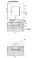
本発明の第1実施の形態に係る半導体装置の製造方法の第1例を、図1ないし図3の製造工程図によって説明する。図1、図2の製造工程図では、各図の上側の図に平面図を示し、下側の図に上記平面図におけるA−A’線断面図を示した。図3の製造工程図では断面図を示した。<1. First Embodiment>
[First Example of Manufacturing Method of Semiconductor Device]
A first example of a method of manufacturing a semiconductor device according to the first embodiment of the present invention will be described with reference to manufacturing process diagrams of FIGS. In the manufacturing process diagrams of FIGS. 1 and 2, a plan view is shown in an upper diagram of each figure, and a cross-sectional view taken along line AA ′ in the plan view is shown in a lower diagram. The manufacturing process diagram of FIG. 3 shows a cross-sectional view.
図1(1)に示すように、第1基板11上に第1層間絶縁膜12が形成され、この第1層間絶縁膜12に形成された第1溝13内に第1バリアメタル層14を介して第1金属電極15が埋め込まれている。このような第1基板11を用意する。
上記第1基板11には、例えばシリコン基板が用いられ、通常のLSIプロセスにより、半導体素子(図示せず)の形成、配線(図示せず)の形成等を行った後、層間絶縁膜が形成されている。この層間絶縁膜の最上層の上記第1層間絶縁膜12に、通常の溝配線形成技術(例えば、ダマシン加工法、デュアルダマシン加工法等)により第1溝13内に第1金属電極15を形成する。
上記第1金属電極15は、例えば50μm角の方形で厚さが500nmに形成され、その表面は、上記第1層間絶縁膜12の表面と同一高さに形成されている。すなわち、上記第1層間絶縁膜12の表面と上記第1金属電極15の表面とは、段差がなく、いわゆる同一平面上にある。上記第1金属電極15は、例えば、銅で形成されている。もちろん、他の金属、例えば、銅、金、銀のうちの1種、もしくはこれらの金属を2種以上用いた合金であってもよい。または、これらの金属を主材料とする合金であってもよい。As shown in FIG. 1A, a first
For example, a silicon substrate is used as the first substrate 11, and a semiconductor element (not shown) is formed, a wiring (not shown) is formed by a normal LSI process, and then an interlayer insulating film is formed. Has been. A
The
また、図2(1)に示すように、第2基板21上に第2層間絶縁膜22が形成され、この第2層間絶縁膜22に形成された第2溝23内に第2バリアメタル層24を介して第2金属電極25が埋め込まれている。このような第2基板21を用意する。
上記第2基板21には、例えばシリコン基板が用いられ、通常のLSIプロセスにより、半導体素子(図示せず)の形成、配線(図示せず)の形成等を行った後、層間絶縁膜が形成されている。この層間絶縁膜の最上層の上記第2層間絶縁膜22に、通常の溝配線形成技術(例えば、ダマシン加工法、デュアルダマシン加工法等)により第2溝23内に第2金属電極25を形成する。
上記第2金属電極25は、例えば50μm角の方形で厚さが500nmに形成され、その表面は、上記第2層間絶縁膜22の表面と同一高さに形成されている。すなわち、上記第2層間絶縁膜22の表面と上記第2金属電極25の表面とは、段差がなく、いわゆる同一平面上にある。上記第2金属電極25は、例えば、銅で形成されている。もちろん、他の金属、例えば、銅、金、銀のうちの1種、もしくはこれらの金属を2種以上用いた合金であってもよい。または、これらの金属を主材料とする合金であってもよい。Further, as shown in FIG. 2A, a second
For example, a silicon substrate is used as the second substrate 21, and after forming a semiconductor element (not shown), forming a wiring (not shown), etc. by a normal LSI process, an interlayer insulating film is formed. Has been. A
The
次に、上記第1層間絶縁膜12もしくは上記第2層間絶縁膜22の少なくとも一方側に層間絶縁膜上に拡散防止層を形成する。ここでは両方の層間絶縁膜に拡散防止層を形成する。
図1(2)に示すように、上記第1層間絶縁膜12の表面に上記第1金属電極15を被覆する第1拡散防止層16を形成する。この第1拡散防止層16は銅の拡散を阻止する材料で形成される。例えば、窒化シリコン化合物または炭化酸化シリコン化合物で形成される。上記窒化シリコン化合物としては窒化シリコン(SiN)があり、上記炭化酸化シリコン化合物としては炭化酸化シリコン(SiOC)があり、また窒化炭化酸化シリコン(SiOCN)を用いることもできる。その膜厚は、銅の拡散を防止し、また第1金属電極15側への酸素の侵入を阻止する膜厚であればよく、例えば、35nm以上50nm以下に形成されている。
例えば、上記第1拡散防止層16を窒化シリコンで形成する場合の成膜条件は、一例として、プラズマCVD法を用いる。そのプロセス条件は、例えば、プロセスガスにアンモニア(NH3)と、窒素(N2)を用い、成膜雰囲気にアンモニア(NH3)を50cm3/min、窒素(N2)を500cm3/minの流量で供給する。成膜雰囲気の圧力を665Pa、基板温度を350℃、プラズマCVD装置のRFパワーを1000W(13.56MHz)に設定する。この条件で、上記第1拡散防止層16を50nmの膜厚に成膜した。Next, a diffusion prevention layer is formed on the interlayer insulating film on at least one side of the first
As shown in FIG. 1B, a first
For example, as a film forming condition when the first
同様に、図2(2)に示すように、上記第2層間絶縁膜22の表面に上記第2金属電極25を被覆する第2拡散防止層26を形成する。この第2拡散防止層26は銅の拡散を阻止する材料で形成される。例えば、窒化シリコン化合物または炭化酸化シリコン化合物で形成される。上記窒化シリコン化合物としては窒化シリコン(SiN)があり、上記炭化酸化シリコン化合物としては炭化酸化シリコン(SiOC)があり、また窒化炭化酸化シリコン(SiOCN)を用いることもできる。その膜厚は、銅の拡散を防止し、また第2金属電極25側への酸素の侵入を阻止する膜厚であればよく、例えば、30nm以上50nm以下に形成されている。
例えば、上記第2拡散防止層26を窒化シリコンで形成する場合の成膜条件は、一例として、プラズマCVD法を用いる。そのプロセス条件は、例えば、プロセスガスにアンモニア(NH3)と、窒素(N2)を用い、成膜雰囲気にアンモニア(NH3)を50cm3/min、窒素(N2)を500cm3/minの流量で供給する。成膜雰囲気の圧力を665Pa、基板温度を350℃、プラズマCVD装置のRFパワーを1000W(13.56MHz)に設定する。この条件で、上記第2拡散防止層26を50nmの膜厚に成膜した。Similarly, as shown in FIG. 2 (2), a second
For example, as a film forming condition when the second
上記第1拡散防止層16、第2拡散防止層26には、銅銅の拡散を阻止する膜としてプラズマCVD法による窒化シリコン膜を用いたが、その他の製法(例えば高周波スパッタ法や高密度プラズマ(High density Plasma)法)を用いて成膜しても良い。また、窒化シリコン膜の他に、上記したように炭化酸化シリコン(SiOC)膜、窒化炭化酸化シリコン(SiOCN)膜を用いることもできる。
上記窒化シリコン膜も炭化酸化シリコン(SiOC)膜も窒化炭化酸化シリコン(SiOCN)膜も、バリア性についての差はない。例えば、400℃の熱処理によって窒化シリコン膜も炭化酸化シリコン膜も窒化炭化酸化シリコン(SiOCN)膜も、膜中への銅の拡散は、20nm程度である。したがって、窒化シリコン膜、炭化酸化シリコン膜、窒化炭化酸化シリコン(SiOCN)膜ともに、30nm以上の膜厚を有すれば、銅のバリア性は十分に確保できる。As the first
There is no difference in barrier properties between the silicon nitride film, the silicon carbide oxide (SiOC) film, and the silicon nitride carbonized oxide (SiOCN) film. For example, the diffusion of copper into the silicon nitride film, silicon carbide oxide film, and silicon nitride oxide (SiOCN) film by heat treatment at 400 ° C. is about 20 nm. Therefore, if the silicon nitride film, the silicon carbide oxide film, and the silicon nitride carbide oxide (SiOCN) film have a film thickness of 30 nm or more, the barrier property of copper can be sufficiently secured.
次に、図1(3)に示すように、上記第1金属電極15と上記第2金属電極25(前記図2(2)参照)を対向して接合する際に、上記第1金属電極15と上記第2金属電極25のそれぞれの形成領域内の上記第1拡散防止層16に第1開口部17を形成する。
上記第1開口部17は、例えば、平面レイアウト上、30μm角の方形に形成される。この第1開口部17の大きさは、適宜、決定される。例えば、後の工程における熱処理時に、上記第1金属電極15が熱膨張をした際に、上記第1開口部17が埋め込まれる大きさに形成される。ここでは、上記条件を満たす大きさとして30μm角の方形とした。
上記第1開口部17は、例えば、上記第1拡散防止層16が窒化シリコン膜で形成されている場合、例えばフッ素系のエッチングガスを用いた反応性イオンエッチング(RIE)によって形成される。Next, as shown in FIG. 1 (3), when the
The
For example, when the first
また、図2(3)に示すように、上記第1金属電極15(前記図1(2)参照)と上記第2金属電極25を対向して接合する際に、上記第1金属電極15と上記第2金属電極25のそれぞれの形成領域内の上記第2拡散防止層26に第2開口部27を形成する。
上記第2開口部27は、例えば、平面レイアウト上、上記第1開口部17(前記図1(3)参照)よりも小さい10μm角の方形に形成される。この第2開口部27の大きさは、適宜、決定される。例えば、後の工程における熱処理時に、上記第2金属電極25が熱膨張をした際に、上記第2開口部27が埋め込まれる大きさに形成される。ここでは、上記条件を満たす大きさとして10μm角の方形とした。もちろん、上記第1開口部17と同様な大きさとしてもよい。
上記第2開口部27は、例えば、上記第2拡散防止層26が窒化シリコン膜で形成されている場合、例えばフッ素系のエッチングガスを用いた反応性イオンエッチング(RIE)によって形成される。Further, as shown in FIG. 2 (3), when the first metal electrode 15 (see FIG. 1 (2)) and the
The
For example, when the second
なお、上記第1開口部17と第2開口部27の大きさを違えることによって、後の熱処理の工程において、開口の大きさが小さい上記第2開口部27に充填される金属が上記第1開口部17側にはみ出す。これによって、第1金属電極15と第2金属電極25との熱膨張による接合が強固になる。このとき、上記第2開口部27に充填される金属が上記第1開口部17側にはみ出したとしても、上記第1開口部17側には空間的余裕があるので、上記はみ出した金属が上記第1拡散防止層16と上記第2拡散防止層26との間に入り込むことはない。 Note that by making the
次に、図1(4)に示すように、上記第1金属電極15表面に形成された酸化膜を除去する前処理を行う。この前処理は、例えば、水素プラズマ処理による還元処理による。
例えば、上記第1金属電極15が銅で形成されている場合には、プロセスガスに水素(H2)とアルゴン(Ar)を用い、還元処理雰囲気に例えば水素を100cm3/minの流量で、アルゴンを170cm3/minの流量で供給する。また、水素プラズマ処理のマイクロ波パワーを2.8kW(2.45GHz)、還元雰囲気の圧力を0.4Pa、基板温度を400℃、還元処理時間を1分とした。この条件は一例であって、適宜、変更可能である。また、上記第1金属電極15表面に酸化膜が形成されていない場合、例えば上記第1金属電極15が金で形成されている場合には、上記水素還元処理を行う必要がない。Next, as shown in FIG. 1 (4), a pretreatment for removing the oxide film formed on the surface of the
For example, when the
同様に、図2(4)に示すように、上記第2金属電極25表面に形成された酸化膜を除去する前処理を行う。この前処理は、例えば、水素プラズマ処理による還元処理による。
例えば、上記第2金属電極25が銅で形成されている場合には、プロセスガスに水素(H2)とアルゴン(Ar)を用い、還元処理雰囲気に例えば水素を100cm3/minの流量で、アルゴンを170cm3/minの流量で供給する。また、水素プラズマ処理のマイクロ波パワーを2.8kW(2.45GHz)、還元雰囲気の圧力を0.4Pa、基板温度を400℃、還元処理時間を1分とした。この条件は一例であって、適宜、変更可能である。また、上記第2金属電極25表面に酸化膜が形成されていない場合、例えば上記第2金属電極25が金で形成されている場合には、上記水素還元処理を行う必要がない。
また、上記のように水素プラズマによる前処理の代わりに、例えば、水素アニール、フォーミングガス(窒素(N2)/水素(H2))によるアニール、アンモニア(NH3)プラズマ、蟻酸プラズマ等による還元処理を行っても良い。Similarly, as shown in FIG. 2 (4), a pretreatment for removing the oxide film formed on the surface of the
For example, when the
Further, instead of the pretreatment with hydrogen plasma as described above, for example, hydrogen annealing, annealing with forming gas (nitrogen (N2 ) / hydrogen (H2 )), reduction with ammonia (NH3 ) plasma, formic acid plasma, etc. Processing may be performed.
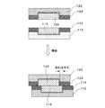
次に、図3(5)に示すように、上記第1開口部17と上記第2開口部27を挟んで上記第1金属電極15と上記第2金属電極25を対向させる。 Next, as shown in FIG. 3 (5), the
そして、図3(6)に示すように、上記第1開口部17と上記第2開口部27を対向させ、上記第1拡散防止層16と上記第2拡散防止層26とを圧して接合させた状態で、熱処理を行う。そして、上記第1金属電極15と上記第2金属電極25の熱膨張によって、上記第1開口部17と上記第2開口部27を通じて上記第1金属電極15と上記第2金属電極25接合させる。
すなわち、熱処理によって、上記第1金属電極15は膨張する。このとき、第1金属電極15は上記第1開口部17以外、第1層間絶縁膜12によって固定されているため、上記第1開口部17側に膨張する。同様に、上記第2金属電極25も膨張する。このとき、第2金属電極25は上記第2開口部27以外、第2層間絶縁膜22によって固定されているため、上記第2開口部27側に膨張する。
そして、互いに膨張した第1金属電極15と第2金属電極25とが、第1開口部17と第2開口部27内で接合し、膨張の圧力によって圧着される。
このとき、上記第1拡散防止層16と上記第2拡散防止層26とを圧して接合させた状態となっているので、膨張した金属電極の金属が第1拡散防止層16と上記第2拡散防止層26との間に入り込むことはない。
なお、上記第1開口部17内および上記第2開口部27内が、上記熱処理による上記第1金属電極15および上記第2金属電極25の膨張した部分で埋め込まれることが望ましい。そのため、第1金属電極15と第2金属電極25の体積膨張量を考慮して、上記第1開口部17と上記第2開口部27の大きさを決定することが好ましい。Then, as shown in FIG. 3 (6), the
That is, the
And the
At this time, since the first
The
上記半導体装置の製造方法では、第1金属電極15と第2金属電極25の熱膨張(体積膨張)を利用しているので、金属を高温、例えば500℃以上で加熱する必要はなく、接合時の加熱温度を、約450℃以下、好ましくは400℃以下にすることができる。そして、第1金属電極15と第2金属電極25の体積膨張により、第1開口部17と第2開口部27内が自己整合的に第1金属電極15と第2金属電極25の金属が充填されて接合することが可能となる。 In the semiconductor device manufacturing method, since the thermal expansion (volume expansion) of the
例えば、上記第1金属電極15(大きさが50μm角の方形、厚さが500nm)の場合、銅の線膨張係数αは16.8×10⁻⁶(1/T)であり、銅の体積膨張係数βは3αである。例えば、上記第1金属電極15を23℃から400℃に加熱した場合を想定すると、第1金属電極15の膨張体積Xは下記のようになる。For example, in the case of the first metal electrode 15 (a square having a size of 50 μm square and a thickness of 500 nm), the linear expansion coefficient α of copper is 16.8 × 10⁻⁶ (1 / T), and the volume of copper The expansion coefficient β is 3α. For example, assuming that the
X=β×(400-23)×50μm×50μm×0.5μm=23.8μm3X = β × (400-23) × 50 μm × 50 μm × 0.5 μm = 23.8 μm3
また、例えば450℃に加熱した場合、X=26.9μm3となる。このとき、第1金属電極15上に30μm角の方形の第1開口部17が形成されていた場合、第1拡散防止層16の厚さが50nmであるから、第1開口部17内に膨張してきた第1金属電極15は、第1拡散防止層16表面から約20nm凹んだ位置まで膨張する。したがって、第1金属電極15の銅が膨張した残りの第1開口部17は約18μm3となる。
また、第2金属電極25上に10μm角の方形の第2開口部27を形成した場合、第2拡散防止層26の厚さが50nmであるから、第2金属電極25の膨張は第2拡散防止層26表面から約156nm凸の形状となる。すなわち、第2開口部27からはみ出した銅の膨張分は約18μm3となる。このように温度を制御することで、過不足無く、第1開口部17と第2開口部27を充填することが可能となる。For example, when heated to 450 ° C., X = 26.9 μm3 . At this time, when the 30 μm square
Further, when the 10 μm square
したがって、第1金属電極15、第2金属電極25のそれぞれの体積、第1開口部17、第2開口部27のそれぞれの面積を決めることによって、双方の接合部分の形状を加熱温度で制御することが可能となる。 Therefore, by determining the respective volumes of the
上記半導体装置の製造方法では、たとえ、第1基板11と第2基板21とで合わせズレが発生したとしても、上記第1金属電極15の第1開口部17側は、上記第1拡散防止層16によって被覆されている。また上記第2金属電極25の第2開口部27側は、上記第1拡散防止層16によって被覆されている。すなわち、上記第1金属電極15は、上記第1バリアメタル層14と上記第1拡散防止層16で囲まれている。また、上記第2金属電極25は、上記第2バリアメタル層24と上記第1拡散防止層16で囲まれている。このため、合わせずれの問題が解消できる。 In the semiconductor device manufacturing method, even if misalignment occurs between the first substrate 11 and the second substrate 21, the
[半導体装置の製造方法の第2例]
本発明の第1実施の形態に係る半導体装置の製造方法の第2例を、図4ないし図6の製造工程図によって説明する。図4、図5の製造工程図では、各図の上側の図に平面図を示し、下側の図に上記平面図におけるA−A’線断面図を示した。図6の製造工程図では断面図を示した。[Second Example of Manufacturing Method of Semiconductor Device]
A second example of the method for manufacturing the semiconductor device according to the first embodiment of the present invention will be described with reference to the manufacturing process diagrams of FIGS. In the manufacturing process diagrams of FIGS. 4 and 5, a plan view is shown in the upper diagram of each figure, and a cross-sectional view along the line AA ′ in the plan view is shown in the lower diagram. The manufacturing process diagram of FIG. 6 shows a cross-sectional view.
図4(1)に示すように、第1基板11上に第1層間絶縁膜12が形成され、この第1層間絶縁膜12に形成された第1溝13内に第1バリアメタル層14を介して第1金属電極15が埋め込まれている。このような第1基板11を用意する。
上記第1基板11には、例えばシリコン基板が用いられ、通常のLSIプロセスにより、半導体素子(図示せず)の形成、配線(図示せず)の形成等を行った後、層間絶縁膜が形成されている。この層間絶縁膜の最上層の上記第1層間絶縁膜12に、通常の溝配線形成技術(例えば、ダマシン加工法、デュアルダマシン加工法等)により第1溝13内に第1バリアメタル層14を介して第1金属電極15を形成する。
上記第1金属電極15は、例えば50μm角の方形で厚さが500nmに形成され、その表面は、上記第1層間絶縁膜12の表面と同一高さに形成されている。すなわち、上記第1層間絶縁膜12の表面と上記第1金属電極15の表面とは、段差がなく、いわゆる同一平面上にある。上記第1金属電極15は、例えば、銅で形成されている。もちろん、他の金属、例えば、銅、金、銀のうちの1種、もしくはこれらの金属を2種以上用いた合金であってもよい。または、これらの金属を主材料とする合金であってもよい。As shown in FIG. 4A, a first
For example, a silicon substrate is used as the first substrate 11, and a semiconductor element (not shown) is formed, a wiring (not shown) is formed by a normal LSI process, and then an interlayer insulating film is formed. Has been. A first
The
また、図5(1)に示すように、第2基板21上に第2層間絶縁膜22が形成され、この第2層間絶縁膜22に形成された第2溝23内に第2バリアメタル層24を介して第2金属電極25が埋め込まれている。このような第2基板21を用意する。
上記第2基板21には、例えばシリコン基板が用いられ、通常のLSIプロセスにより、半導体素子(図示せず)の形成、配線(図示せず)の形成等を行った後、層間絶縁膜が形成されている。この層間絶縁膜の最上層の上記第2層間絶縁膜22に、通常の溝配線形成技術(例えば、ダマシン加工法、デュアルダマシン加工法等)により第2溝23内に第2バリアメタル層24を介して第2金属電極25を形成する。
上記第2金属電極25は、例えば50μm角の方形で厚さが500nmに形成され、その表面は、上記第2層間絶縁膜22の表面と同一高さに形成されている。すなわち、上記第2層間絶縁膜22の表面と上記第2金属電極25の表面とは、段差がなく、いわゆる同一平面上にある。上記第2金属電極25は、例えば、銅で形成されている。もちろん、他の金属、例えば、銅、金、銀のうちの1種、もしくはこれらの金属を2種以上用いた合金であってもよい。または、これらの金属を主材料とする合金であってもよい。Further, as shown in FIG. 5A, a second
For example, a silicon substrate is used as the second substrate 21, and after forming a semiconductor element (not shown), forming a wiring (not shown), etc. by a normal LSI process, an interlayer insulating film is formed. Has been. A second
The
次に、上記第1層間絶縁膜12もしくは上記第2層間絶縁膜22の少なくとも一方側に層間絶縁膜上に拡散防止層を形成する。ここでは両方の層間絶縁膜に拡散防止層を形成する。
図4(2)に示すように、上記第1層間絶縁膜12の表面に第1拡散防止層16を形成する。この第1拡散防止層16は銅の拡散を阻止する材料で形成される。例えば、窒化シリコン化合物または炭化酸化シリコン化合物で形成される。上記窒化シリコン化合物としては窒化シリコン(SiN)があり、上記炭化酸化シリコン化合物としては炭化酸化シリコン(SiOC)があり、また窒化炭化酸化シリコン(SiOCN)を用いることもできる。その膜厚は、銅の拡散を防止し、また第1金属電極15側への酸素の侵入を阻止する膜厚であればよく、例えば、30nm以上50nm以下に形成されている。
例えば、上記第1拡散防止層16を窒化シリコンで形成する場合の成膜条件は、一例として、プラズマCVD法を用いる。そのプロセス条件は、例えば、プロセスガスにアンモニア(NH3)と、窒素(N2)を用い、成膜雰囲気にアンモニア(NH3)を50cm3/min、窒素(N2)を500cm3/minの流量で供給する。成膜雰囲気の圧力を665Pa、基板温度を350℃、プラズマCVD装置のRFパワーを1000W(13.56MHz)に設定する。この条件で、上記第1拡散防止層16を50nmの膜厚に成膜した。Next, a diffusion prevention layer is formed on the interlayer insulating film on at least one side of the first
As shown in FIG. 4B, a first
For example, as a film forming condition when the first
上記第1拡散防止層16には、銅の拡散を阻止する膜としてプラズマCVD法による窒化シリコン膜を用いたが、その他の製法(例えば高周波スパッタ法や高密度プラズマ(High density Plasma)法)を用いて成膜しても良い。また、窒化シリコン膜の他に、上記したように炭化酸化シリコン(SiOC)膜、窒化炭化酸化シリコン(SiOCN)膜を用いることもできる。
上記窒化シリコン膜も炭化酸化シリコン(SiOC)膜も窒化炭化酸化シリコン(SiOCN)膜も、バリア性については、差はない。例えば、400℃の熱処理によって窒化シリコン膜も炭化酸化シリコン膜中への銅の拡散は、20nm程度である。したがって、窒化シリコン膜、炭化酸化シリコン膜、窒化炭化酸化シリコン(SiOCN)膜ともに、30nm以上の膜厚を有すれば、銅のバリア性は十分に確保できる。As the first
There is no difference in barrier properties between the silicon nitride film, the silicon carbide oxide (SiOC) film, and the nitrided silicon carbide oxide (SiOCN) film. For example, the diffusion of copper into the silicon nitride film and the silicon nitride film by heat treatment at 400 ° C. is about 20 nm. Therefore, if the silicon nitride film, the silicon carbide oxide film, and the silicon nitride carbide oxide (SiOCN) film have a film thickness of 30 nm or more, the barrier property of copper can be sufficiently secured.
次に、図4(3)に示すように、上記第1金属電極15と上記第2金属電極25(前記図5(1)参照)を対向して接合する際に、上記第1金属電極15と上記第2金属電極25のそれぞれの形成領域内の上記第1拡散防止層16に第1開口部17を形成する。
上記第1開口部17は、例えば、平面レイアウト上、30μm角の方形に形成される。この第1開口部17の大きさは、適宜、決定される。例えば、後の工程における熱処理時に、上記第1金属電極15が熱膨張をした際に、上記第1開口部17が埋め込まれる大きさに形成される。ここでは、上記条件を満たす大きさとして30μm角の方形とした。
上記第1開口部17は、例えば、上記第1拡散防止層16が窒化シリコン膜で形成されている場合、例えばフッ素系のエッチングガスを用いた反応性イオンエッチング(RIE)によって形成される。Next, as shown in FIG. 4 (3), when the
The
For example, when the first
次に、図4(4)に示すように、上記第1金属電極15表面に形成された酸化膜を除去する前処理を行う。この前処理は、例えば、水素プラズマ処理による還元処理による。
例えば、上記第1金属電極15が銅で形成されている場合には、プロセスガスに水素(H2)とアルゴン(Ar)を用い、還元処理雰囲気に例えば水素を100cm3/minの流量で、アルゴンを170cm3/minの流量で供給する。また、水素プラズマ処理のマイクロ波パワーを2.8kW(2.45GHz)、還元雰囲気の圧力を0.4Pa、基板温度を400℃、還元処理時間を1分とした。この条件は一例であって、適宜、変更可能である。また、上記第1金属電極15表面に酸化膜が形成されていない場合、例えば上記第1金属電極15が金で形成されている場合には、上記水素還元処理を行う必要がない。Next, as shown in FIG. 4 (4), a pretreatment for removing the oxide film formed on the surface of the
For example, when the
同様に、図5(2)に示すように、上記第2金属電極25表面に形成された酸化膜を除去する前処理を行う。この前処理は、例えば、水素プラズマ処理による還元処理による。
例えば、上記第2金属電極25が銅で形成されている場合には、プロセスガスに水素(H2)とアルゴン(Ar)を用い、還元処理雰囲気に例えば水素を100cm3/minの流量で、アルゴンを170cm3/minの流量で供給する。また、水素プラズマ処理のマイクロ波パワーを2.8kW(2.45GHz)、還元雰囲気の圧力を0.4Pa、基板温度を400℃、還元処理時間を1分とした。この条件は一例であって、適宜、変更可能である。また、上記第2金属電極25表面に酸化膜が形成されていない場合、例えば上記第2金属電極25が金で形成されている場合には、上記水素還元処理を行う必要がない。
また、上記のように水素プラズマによる前処理の代わりに、例えば、水素アニール、フォーミングガス(窒素(N2)/水素(H2))によるアニール、アンモニア(NH3)プラズマ、蟻酸プラズマ等による還元処理を行っても良い。Similarly, as shown in FIG. 5B, a pretreatment for removing the oxide film formed on the surface of the
For example, when the
Further, instead of the pretreatment with hydrogen plasma as described above, for example, hydrogen annealing, annealing with forming gas (nitrogen (N2 ) / hydrogen (H2 )), reduction with ammonia (NH3 ) plasma, formic acid plasma, etc. Processing may be performed.
次に、図6(5)に示すように、上記第1開口部17を挟んで上記第1金属電極15と上記第2金属電極25を対向させる。 Next, as shown in FIG. 6 (5), the
そして、図6(6)に示すように、上記第1拡散防止層16と、上記第2金属電極25、上記第2層間絶縁膜22とを圧して接合させた状態で、熱処理を行う。そして、上記第1金属電極15と上記第2金属電極25の熱膨張によって、上記第1開口部17を通じて上記第1金属電極15と上記第2金属電極25を接合させる。
すなわち、熱処理によって、上記第1金属電極15は膨張する。このとき、第1金属電極15は上記第1開口部17以外、第1層間絶縁膜12によって固定されているため、上記第1開口部17側に膨張する。同様に、上記第2金属電極25も膨張する。このとき、第2金属電極25は上記第1開口部17以外、第2層間絶縁膜22によって固定されているため、上記第1開口部17側に膨張する。
そして、互いに膨張した第1金属電極15と第2金属電極25とが、第1開口部17内で接合し、膨張の圧力によって圧着される。
このとき、上記第1拡散防止層16と、上記第2金属電極25、上記第2層間絶縁膜22とを圧して接合させた状態となっているので、膨張した金属電極の金属が第1拡散防止層16と上記第2層間絶縁膜22との間に入り込むことはない。
なお、上記第1開口部17内が、上記熱処理による上記第1金属電極15および上記第2金属電極25の膨張した部分で埋め込まれることが望ましい。そのため、第1金属電極15と第2金属電極25の体積膨張量を考慮して、上記第1開口部17の大きさを決定することが好ましい。Then, as shown in FIG. 6 (6), heat treatment is performed in a state where the first
That is, the
And the
At this time, since the first
The
上記半導体装置の製造方法(第2例)では、たとえ、第1基板11と第2基板21とで合わせズレが発生したとしても、第1金属電極15、第2金属電極25の第1開口部17側は、上記第1拡散防止層16によって被覆されている。すなわち、上記第1金属電極15は、上記第1バリアメタル層14と上記第1拡散防止層16で囲まれている。また、上記第2金属電極25は、上記第2バリアメタル層24と上記第1拡散防止層16で囲まれている。このため、合わせずれの問題が解消できる。 In the semiconductor device manufacturing method (second example), even if misalignment occurs between the first substrate 11 and the second substrate 21, the first openings of the
また、第1金属電極15と第2金属電極25の熱膨張(体積膨張)を利用しているので、接合時の加熱温度を、約400℃以下にすることもできる。さらに、第1金属電極15と第2金属電極25の体積膨張量により、第1開口部17内が自己整合的に第1金属電極15と第2金属電極25の金属が充填されて接合することが可能となる。 Further, since the thermal expansion (volume expansion) of the
上記第1例、第2例ともに、熱処理方法は通常の電気炉、ランプ加熱炉等を用いた熱処理が行える。上記熱処理時の雰囲気は、真空状態であっても、不活性ガス雰囲気であってもよい。また、マイクロ波加熱を利用することもできる。 In both the first and second examples, the heat treatment can be performed using a normal electric furnace, lamp heating furnace, or the like. The atmosphere during the heat treatment may be a vacuum state or an inert gas atmosphere. Microwave heating can also be used.
<2.第2の実施の形態>
[半導体装置の構成の一例]
本発明の第2実施の形態に係る半導体装置の構成の一例を、図7の概略構成断面図によって説明する。<2. Second Embodiment>
[Example of configuration of semiconductor device]
An example of the configuration of the semiconductor device according to the second embodiment of the present invention will be described with reference to the schematic cross-sectional view of FIG.
図7に示すように、第1基板11上に第1層間絶縁膜12が形成され、この第1層間絶縁膜12に形成された第1溝13内に第1バリアメタル層14を介して第1金属電極15が埋め込まれている。
上記第1基板11には、例えばシリコン基板が用いられ、このシリコン基板には、半導体素子(図示せず)、配線(図示せず)等が形成され、さらに層間絶縁膜が形成されている。この層間絶縁膜の最上層の層間絶縁膜が上記第1層間絶縁膜12である。
上記第1金属電極15は、例えば50μm角の方形で厚さが500nmに形成されている。上記第1金属電極15は、例えば、銅で形成されている。もちろん、他の金属、例えば、銅、金、銀のうちの1種、もしくはこれらの金属を2種以上用いた合金であってもよい。または、これらの金属を主材料とする合金であってもよい。As shown in FIG. 7, a first
For example, a silicon substrate is used as the first substrate 11. A semiconductor element (not shown), wiring (not shown), and the like are formed on the silicon substrate, and an interlayer insulating film is further formed. The uppermost interlayer insulating film of the interlayer insulating film is the first
The
また、第2基板21上に第2層間絶縁膜22が形成され、この第2層間絶縁膜22に形成された第2溝23内に第2バリアメタル層24を介して第2金属電極25が埋め込まれている。
上記第2基板21には、例えばシリコン基板が用いられ、このシリコン基板には、半導体素子(図示せず)、配線(図示せず)等が形成され、さらに層間絶縁膜が形成されている。この層間絶縁膜の最上層の層間絶縁膜が上記第2層間絶縁膜22である。
上記第2金属電極25は、例えば50μm角の方形で厚さが500nmに形成されている。上記第2金属電極25は、例えば、銅で形成されている。もちろん、他の金属、例えば、銅、金、銀のうちの1種、もしくはこれらの金属を2種以上用いた合金であってもよい。または、これらの金属を主材料とする合金であってもよい。In addition, a second
For example, a silicon substrate is used as the second substrate 21. A semiconductor element (not shown), wiring (not shown), and the like are formed on the silicon substrate, and an interlayer insulating film is further formed. The uppermost interlayer insulating film of this interlayer insulating film is the second
The
上記第1層間絶縁膜12と上記第2層間絶縁膜22間には第1拡散防止層16が形成されている。この第1拡散防止層16は銅の拡散を阻止する材料で形成される。例えば、窒化シリコン膜で形成される。その膜厚は、銅の拡散を防止し、また第1金属電極15、第2金属電極25の両方への酸素の侵入を阻止する膜厚であればよく、例えば、35nm以上50nm以下に形成されている。 A first
上記第1拡散防止層16には、銅の拡散を阻止する膜としてプラズマCVD法による窒化シリコン膜を用いたが、その他の製法(例えば高周波スパッタ法や高密度プラズマ(High density Plasma)法)を用いた膜としても良い。また、窒化シリコン膜の他に、炭化酸化シリコン(SiOC)膜を用いることもできる。 As the first
上記第1拡散防止層16には、上記第1金属電極15と上記第2金属電極25のそれぞれの形成領域内に第1開口部17が形成されている。
上記第1開口部17は、例えば、平面レイアウト上、30μm角の方形に形成される。この第1開口部17の大きさは、適宜、決定される。例えば、後の工程における熱処理時に、上記第1金属電極15および第2金属電極25が熱膨張をした際に、上記第1開口部17が埋め込まれる大きさに形成される。ここでは、上記条件を満たす大きさとして30μm角の方形とした。In the first
The
上記第1開口部17を挟んで上記第1金属電極15と上記第2金属電極25とが対向して接合している。この接合は、例えば上記第1金属電極15と上記第2金属電極25の熱膨張によって、熱圧着による。
なお、上記第1開口部17内が、上記第1金属電極15および上記第2金属電極25の膨張した部分で埋め込まれることが望ましい。The
The
上記半導体装置では、たとえ、第1基板11と第2基板21とで合わせズレが発生したとしても、第1金属電極15、第2金属電極25の第1開口部17側は、上記第1拡散防止層16によって被覆されている。すなわち、上記第1金属電極15は、上記第1バリアメタル層14と上記第1拡散防止層16で囲まれている。また、上記第2金属電極25は、上記第2バリアメタル層24と上記第1拡散防止層16で囲まれている。このため、合わせずれの問題が解消できる。 In the semiconductor device, even if misalignment occurs between the first substrate 11 and the second substrate 21, the
11…第1基板、12…第1層間絶縁膜、13…第1溝、15…第1金属電極、16…第1拡散防止層、17…第1開口部、21…第2基板、22…第2層間絶縁膜、23…第2溝、25…第2金属電極、26…第2拡散防止層、27…第2開口部 DESCRIPTION OF SYMBOLS 11 ... 1st board | substrate, 12 ... 1st interlayer insulation film, 13 ... 1st groove | channel, 15 ... 1st metal electrode, 16 ... 1st diffusion prevention layer, 17 ... 1st opening part, 21 ... 2nd board | substrate, 22 ... Second interlayer insulating film, 23 ... second groove, 25 ... second metal electrode, 26 ... second diffusion prevention layer, 27 ... second opening
Claims (7)
Translated fromJapanese第2基板上に第2層間絶縁膜が形成され、該第2層間絶縁膜に形成された第2溝内に第2金属電極が埋め込まれた第2基板を用意し、
前記第1層間絶縁膜側に第1拡散防止層を形成する工程と、
前記第2層間絶縁膜側に第2拡散防止層を形成する工程と、
前記第1金属電極と前記第2金属電極を対向して接合する際に、前記第1金属電極と前記第2金属電極のそれぞれの形成領域内の前記第1拡散防止層に第1開口部を形成する工程と、
前記第1金属電極と前記第2金属電極を対向して接合する際に、前記第1金属電極と前記第2金属電極のそれぞれの形成領域内の前記第2拡散防止層に第2開口部を形成する工程と、
前記第1開口部と前記第2開口部を対向させて熱処理を行い、前記第1金属電極と前記第2金属電極を熱膨張によって前記第1開口部と前記第2開口部を通じて接合させる工程を有する
半導体装置の製造方法。Preparing a first substrate in which a first interlayer insulating film is formed on a first substrate, and a first metal electrode is embedded in a first groove formed in the first interlayer insulating film;
Preparing a second substrate in which a second interlayer insulating film is formed on the second substrate, and a second metal electrode is embedded in a second groove formed in the second interlayer insulating film;
Forming a first diffusion barrier layer on the first interlayer insulating film side;
Forming a second diffusion barrier layer on the second interlayer insulating film side;
When the first metal electrode and the second metal electrode are joined to face each other, a first opening is formed in the first diffusion prevention layer in each formation region of the first metal electrode and the second metal electrode. Forming, and
When the first metal electrode and the second metal electrode are joined to face each other, a second opening is formed in the second diffusion prevention layer in each formation region of the first metal electrode and the second metal electrode. Forming, and
Performing a heat treatment with the first opening and the second opening facing each other, and joining the first metal electrode and the second metal electrode through the first opening and the second opening by thermal expansion; A method for manufacturing a semiconductor device.
請求項1記載の半導体装置の製造方法。The method for manufacturing a semiconductor device according to claim 1, wherein the first diffusion prevention layer and the second diffusion prevention layer are made of a silicon nitride compound or a silicon carbide oxide compound.
請求項1または請求項2記載の半導体装置の製造方法。The method for manufacturing a semiconductor device according to claim 1, wherein the first opening and the second opening have an opening area difference.
第2基板上に第2層間絶縁膜が形成され、該第2層間絶縁膜に形成された第2溝内に第2金属電極が埋め込まれた第2基板を用意し、
前記第1層間絶縁膜もしくは前記第2層間絶縁膜の少なくとも一方側に層間絶縁膜上に拡散防止層を形成する工程と、
前記第1金属電極と前記第2金属電極を対向して接合する際に、前記第1金属電極と前記第2金属電極のそれぞれの形成領域内の前記拡散防止層に開口部を形成する工程と、
前記開口部を挟んで前記第1金属電極と前記第2金属電極を対向させて熱処理を行い、前記第1金属電極と前記第2金属電極を熱膨張によって前記開口部を通じて接合させる工程を有する
半導体装置の製造方法。Preparing a first substrate in which a first interlayer insulating film is formed on a first substrate, and a first metal electrode is embedded in a first groove formed in the first interlayer insulating film;
Preparing a second substrate in which a second interlayer insulating film is formed on the second substrate, and a second metal electrode is embedded in a second groove formed in the second interlayer insulating film;
Forming a diffusion prevention layer on the interlayer insulating film on at least one side of the first interlayer insulating film or the second interlayer insulating film;
Forming an opening in the diffusion preventing layer in each of the formation regions of the first metal electrode and the second metal electrode when the first metal electrode and the second metal electrode are joined to face each other; ,
A step of heat-treating the first metal electrode and the second metal electrode facing each other with the opening interposed therebetween, and joining the first metal electrode and the second metal electrode through the opening by thermal expansion; Device manufacturing method.
請求項4記載の半導体装置の製造方法。The method for manufacturing a semiconductor device according to claim 4, wherein the diffusion preventing layer is made of a silicon nitride compound or a silicon carbide oxide compound.
請求項1ないし請求項5のいずれか1項に記載の半導体装置の製造方法。The semiconductor device according to claim 1, wherein the first metal electrode and the second metal electrode are made of copper, gold, or silver, or a plurality of types of alloys thereof. Method.
前記第1層間絶縁膜に形成された第1溝内に埋め込まれた第1金属電極と、
第2基板上に形成された第2層間絶縁膜と、
前記第2層間絶縁膜に形成された第2溝内に埋め込まれた第2金属電極と、
前記第1層間絶縁膜と前記第2層間絶縁膜との間に形成された拡散防止層と、
前記第1金属電極および前記第2金属電極の形成領域内で前記拡散防止層に形成された開口部を有し、
前記開口部を通じて前記第1金属配線と前記第2金属配線とが接合されている
半導体装置。A first interlayer insulating film formed on the first substrate;
A first metal electrode embedded in a first groove formed in the first interlayer insulating film;
A second interlayer insulating film formed on the second substrate;
A second metal electrode embedded in a second groove formed in the second interlayer insulating film;
A diffusion prevention layer formed between the first interlayer insulating film and the second interlayer insulating film;
An opening formed in the diffusion preventing layer in a region where the first metal electrode and the second metal electrode are formed;
The semiconductor device, wherein the first metal wiring and the second metal wiring are joined through the opening.
Priority Applications (1)
| Application Number | Priority Date | Filing Date | Title |
|---|---|---|---|
| JP2009195112AJP5407660B2 (en) | 2009-08-26 | 2009-08-26 | Manufacturing method of semiconductor device |
Applications Claiming Priority (1)
| Application Number | Priority Date | Filing Date | Title |
|---|---|---|---|
| JP2009195112AJP5407660B2 (en) | 2009-08-26 | 2009-08-26 | Manufacturing method of semiconductor device |
Publications (2)
| Publication Number | Publication Date |
|---|---|
| JP2011049270Atrue JP2011049270A (en) | 2011-03-10 |
| JP5407660B2 JP5407660B2 (en) | 2014-02-05 |
Family
ID=43835343
Family Applications (1)
| Application Number | Title | Priority Date | Filing Date |
|---|---|---|---|
| JP2009195112AExpired - Fee RelatedJP5407660B2 (en) | 2009-08-26 | 2009-08-26 | Manufacturing method of semiconductor device |
Country Status (1)
| Country | Link |
|---|---|
| JP (1) | JP5407660B2 (en) |
Cited By (15)
| Publication number | Priority date | Publication date | Assignee | Title |
|---|---|---|---|---|
| JP2012084881A (en)* | 2010-10-14 | 2012-04-26 | Soytec | Process for realizing connecting structure |
| JP2012204501A (en)* | 2011-03-24 | 2012-10-22 | Sony Corp | Semiconductor device, electronic device, and semiconductor device manufacturing method |
| KR20130007972A (en)* | 2011-07-05 | 2013-01-21 | 소니 주식회사 | Semiconductor device, fabrication method for a semiconductor device and electronic apparatus |
| JP2013033786A (en)* | 2011-08-01 | 2013-02-14 | Sony Corp | Semiconductor device and semiconductor device manufacturing method |
| JP2013033900A (en)* | 2011-07-05 | 2013-02-14 | Sony Corp | Semiconductor device, electronic apparatus, method of fabricating semiconductor device |
| JP2013038112A (en)* | 2011-08-04 | 2013-02-21 | Sony Corp | Semiconductor device, semiconductor device manufacturing method and electronic apparatus |
| JP2013073988A (en)* | 2011-09-27 | 2013-04-22 | Sony Corp | Semiconductor device and semiconductor device manufacturing method |
| JP2013118373A (en)* | 2011-12-02 | 2013-06-13 | Samsung Electronics Co Ltd | Electrode connecting structure containing copper |
| JP2013168419A (en)* | 2012-02-14 | 2013-08-29 | Sony Corp | Semiconductor device, method for manufacturing the same, and electronic equipment |
| US9111763B2 (en) | 2011-07-05 | 2015-08-18 | Sony Corporation | Semiconductor device, fabrication method for a semiconductor device and electronic apparatus |
| US9287251B2 (en) | 2014-07-18 | 2016-03-15 | Samsung Electronics Co., Ltd. | Method of manufacturing a semiconductor device |
| WO2018211974A1 (en)* | 2017-05-16 | 2018-11-22 | ソニーセミコンダクタソリューションズ株式会社 | Semiconductor device and method for manufacturing semiconductor device |
| US11127711B2 (en) | 2019-09-10 | 2021-09-21 | Kioxia Corporation | Semiconductor device |
| EP3945566A1 (en)* | 2020-07-29 | 2022-02-02 | Imec VZW | A method for wafer to wafer hybrid bonding, enabling improved metal-to-metal contact and higher density of interconnect pads |
| US12211812B2 (en) | 2021-03-16 | 2025-01-28 | Kioxia Corporation | Semiconductor storage device and method for fabricating semiconductor storage device |
Families Citing this family (2)
| Publication number | Priority date | Publication date | Assignee | Title |
|---|---|---|---|---|
| JP6335099B2 (en) | 2014-11-04 | 2018-05-30 | 東芝メモリ株式会社 | Semiconductor device and manufacturing method of semiconductor device |
| KR102822691B1 (en) | 2020-06-05 | 2025-06-20 | 삼성전자주식회사 | Semiconductor device and semiconductor package including same |
Citations (3)
| Publication number | Priority date | Publication date | Assignee | Title |
|---|---|---|---|---|
| JPH08125121A (en)* | 1994-08-29 | 1996-05-17 | Matsushita Electric Ind Co Ltd | Semiconductor device and manufacturing method thereof |
| JP2000236020A (en)* | 1998-12-17 | 2000-08-29 | Nec Corp | Semiconductor device and manufacture thereof |
| JP2012084881A (en)* | 2010-10-14 | 2012-04-26 | Soytec | Process for realizing connecting structure |
- 2009
- 2009-08-26JPJP2009195112Apatent/JP5407660B2/ennot_activeExpired - Fee Related
Patent Citations (3)
| Publication number | Priority date | Publication date | Assignee | Title |
|---|---|---|---|---|
| JPH08125121A (en)* | 1994-08-29 | 1996-05-17 | Matsushita Electric Ind Co Ltd | Semiconductor device and manufacturing method thereof |
| JP2000236020A (en)* | 1998-12-17 | 2000-08-29 | Nec Corp | Semiconductor device and manufacture thereof |
| JP2012084881A (en)* | 2010-10-14 | 2012-04-26 | Soytec | Process for realizing connecting structure |
Cited By (31)
| Publication number | Priority date | Publication date | Assignee | Title |
|---|---|---|---|---|
| KR101300811B1 (en)* | 2010-10-14 | 2013-08-26 | 소이텍 | Process for realising a connecting structure |
| JP2012084881A (en)* | 2010-10-14 | 2012-04-26 | Soytec | Process for realizing connecting structure |
| US9224704B2 (en) | 2010-10-14 | 2015-12-29 | Soitec | Process for realizing a connecting structure |
| JP2012204501A (en)* | 2011-03-24 | 2012-10-22 | Sony Corp | Semiconductor device, electronic device, and semiconductor device manufacturing method |
| US10985102B2 (en) | 2011-07-05 | 2021-04-20 | Sony Corporation | Semiconductor device, fabrication method for a semiconductor device and electronic apparatus |
| US9911778B2 (en) | 2011-07-05 | 2018-03-06 | Sony Corporation | Semiconductor device, fabrication method for a semiconductor device and electronic apparatus |
| US10431621B2 (en) | 2011-07-05 | 2019-10-01 | Sony Corporation | Semiconductor device, fabrication method for a semiconductor device and electronic apparatus |
| US11569123B2 (en) | 2011-07-05 | 2023-01-31 | Sony Corporation | Semiconductor device, fabrication method for a semiconductor device and electronic apparatus |
| JP2013033900A (en)* | 2011-07-05 | 2013-02-14 | Sony Corp | Semiconductor device, electronic apparatus, method of fabricating semiconductor device |
| KR102298787B1 (en) | 2011-07-05 | 2021-09-07 | 소니그룹주식회사 | Semiconductor device, fabrication method for a semiconductor device and electronic apparatus |
| US9111763B2 (en) | 2011-07-05 | 2015-08-18 | Sony Corporation | Semiconductor device, fabrication method for a semiconductor device and electronic apparatus |
| KR20200070189A (en)* | 2011-07-05 | 2020-06-17 | 소니 주식회사 | Semiconductor device, fabrication method for a semiconductor device and electronic apparatus |
| KR20130007972A (en)* | 2011-07-05 | 2013-01-21 | 소니 주식회사 | Semiconductor device, fabrication method for a semiconductor device and electronic apparatus |
| US9443802B2 (en) | 2011-07-05 | 2016-09-13 | Sony Corporation | Semiconductor device, fabrication method for a semiconductor device and electronic apparatus |
| KR102030852B1 (en)* | 2011-07-05 | 2019-10-10 | 소니 주식회사 | Semiconductor device, fabrication method for a semiconductor device and electronic apparatus |
| US10038024B2 (en) | 2011-07-05 | 2018-07-31 | Sony Corporation | Semiconductor device, fabrication method for a semiconductor device and electronic apparatus |
| JP2013033786A (en)* | 2011-08-01 | 2013-02-14 | Sony Corp | Semiconductor device and semiconductor device manufacturing method |
| JP2013038112A (en)* | 2011-08-04 | 2013-02-21 | Sony Corp | Semiconductor device, semiconductor device manufacturing method and electronic apparatus |
| JP2013073988A (en)* | 2011-09-27 | 2013-04-22 | Sony Corp | Semiconductor device and semiconductor device manufacturing method |
| KR101931491B1 (en)* | 2011-12-02 | 2018-12-24 | 삼성전자주식회사 | Electrodes Connecting Structures Having Copper |
| JP2013118373A (en)* | 2011-12-02 | 2013-06-13 | Samsung Electronics Co Ltd | Electrode connecting structure containing copper |
| JP2013168419A (en)* | 2012-02-14 | 2013-08-29 | Sony Corp | Semiconductor device, method for manufacturing the same, and electronic equipment |
| US9287251B2 (en) | 2014-07-18 | 2016-03-15 | Samsung Electronics Co., Ltd. | Method of manufacturing a semiconductor device |
| WO2018211974A1 (en)* | 2017-05-16 | 2018-11-22 | ソニーセミコンダクタソリューションズ株式会社 | Semiconductor device and method for manufacturing semiconductor device |
| US11257782B2 (en) | 2017-05-16 | 2022-02-22 | Sony Semiconductor Solutions Corporation | Method of manufacturing semiconductor device and semiconductor device |
| US11721664B2 (en) | 2017-05-16 | 2023-08-08 | Sony Semiconductor Solutions Corporation | Method of manufacturing semiconductor device and semiconductor device |
| US12211819B2 (en) | 2017-05-16 | 2025-01-28 | Sony Semiconductor Solutions Corporation | Method of manufacturing semiconductor device and semiconductor device |
| US11127711B2 (en) | 2019-09-10 | 2021-09-21 | Kioxia Corporation | Semiconductor device |
| EP3945566A1 (en)* | 2020-07-29 | 2022-02-02 | Imec VZW | A method for wafer to wafer hybrid bonding, enabling improved metal-to-metal contact and higher density of interconnect pads |
| US11769750B2 (en) | 2020-07-29 | 2023-09-26 | Imec Vzw | Substrate, assembly and method for wafer-to-wafer hybrid bonding |
| US12211812B2 (en) | 2021-03-16 | 2025-01-28 | Kioxia Corporation | Semiconductor storage device and method for fabricating semiconductor storage device |
Also Published As
| Publication number | Publication date |
|---|---|
| JP5407660B2 (en) | 2014-02-05 |
Similar Documents
| Publication | Publication Date | Title |
|---|---|---|
| JP5407660B2 (en) | Manufacturing method of semiconductor device | |
| US11715752B2 (en) | Semiconductor device and method for production of semiconductor device | |
| CN101339924B (en) | Semiconductor device | |
| WO2015040784A1 (en) | Semiconductor device and method for manufacturing same | |
| CN101527300A (en) | Stacked integrated circuit and method of manufacturing the same | |
| JP2013077711A (en) | Semiconductor device and manufacturing method of semiconductor device | |
| JP2003249547A (en) | Connection structure between wirings and manufacturing method thereof | |
| JP2008010534A (en) | Semiconductor device and manufacturing method thereof | |
| JP2002231808A (en) | Semiconductor device and its manufacturing method | |
| US7199043B2 (en) | Method of forming copper wiring in semiconductor device | |
| KR20100040455A (en) | Method for fabricating of semiconductor device | |
| JP2007150301A (en) | Semiconductor device and manufacturing method thereof | |
| US11211348B2 (en) | First wafer, fabricating method thereof and wafer stack | |
| CN100463190C (en) | SOI substrate and its manufacturing method | |
| US11769750B2 (en) | Substrate, assembly and method for wafer-to-wafer hybrid bonding | |
| CN113964080B (en) | Semiconductor device and manufacturing method thereof | |
| KR100960934B1 (en) | Metal wiring of semiconductor device and method of forming the same | |
| JP2008108769A (en) | Manufacturing method of semiconductor device | |
| KR20070024865A (en) | Metal wiring formation method of semiconductor device | |
| JP3087692B2 (en) | Method for manufacturing semiconductor device | |
| US11862607B2 (en) | Composite dielectric structures for semiconductor die assemblies and associated systems and methods | |
| TWI761192B (en) | Method for forming wire | |
| KR100567539B1 (en) | Metal wiring formation method of semiconductor device | |
| CN118969730A (en) | Hybrid bonding method and hybrid bonding structure | |
| KR100790248B1 (en) | Semiconductor device manufacturing method |
Legal Events
| Date | Code | Title | Description |
|---|---|---|---|
| RD02 | Notification of acceptance of power of attorney | Free format text:JAPANESE INTERMEDIATE CODE: A7422 Effective date:20110712 | |
| A621 | Written request for application examination | Free format text:JAPANESE INTERMEDIATE CODE: A621 Effective date:20120731 | |
| A977 | Report on retrieval | Free format text:JAPANESE INTERMEDIATE CODE: A971007 Effective date:20130626 | |
| A131 | Notification of reasons for refusal | Free format text:JAPANESE INTERMEDIATE CODE: A131 Effective date:20130723 | |
| A521 | Request for written amendment filed | Free format text:JAPANESE INTERMEDIATE CODE: A523 Effective date:20130913 | |
| A01 | Written decision to grant a patent or to grant a registration (utility model) | Free format text:JAPANESE INTERMEDIATE CODE: A01 Effective date:20131008 | |
| A61 | First payment of annual fees (during grant procedure) | Free format text:JAPANESE INTERMEDIATE CODE: A61 Effective date:20131021 | |
| LAPS | Cancellation because of no payment of annual fees |