JP2011040742A - Heatsink with periodically patterned baseplate structure, and related device and method (heat sink with periodically patterned baseplate structure) - Google Patents
Heatsink with periodically patterned baseplate structure, and related device and method (heat sink with periodically patterned baseplate structure)Download PDFInfo
- Publication number
- JP2011040742A JP2011040742AJP2010174276AJP2010174276AJP2011040742AJP 2011040742 AJP2011040742 AJP 2011040742AJP 2010174276 AJP2010174276 AJP 2010174276AJP 2010174276 AJP2010174276 AJP 2010174276AJP 2011040742 AJP2011040742 AJP 2011040742A
- Authority
- JP
- Japan
- Prior art keywords
- heat sink
- patches
- electrically conductive
- base
- periodic pattern
- Prior art date
- Legal status (The legal status is an assumption and is not a legal conclusion. Google has not performed a legal analysis and makes no representation as to the accuracy of the status listed.)
- Granted
Links
Images


Classifications
- H—ELECTRICITY
- H01—ELECTRIC ELEMENTS
- H01L—SEMICONDUCTOR DEVICES NOT COVERED BY CLASS H10
- H01L23/00—Details of semiconductor or other solid state devices
- H01L23/34—Arrangements for cooling, heating, ventilating or temperature compensation ; Temperature sensing arrangements
- H01L23/36—Selection of materials, or shaping, to facilitate cooling or heating, e.g. heatsinks
- H01L23/367—Cooling facilitated by shape of device
- H01L23/3677—Wire-like or pin-like cooling fins or heat sinks
- H—ELECTRICITY
- H01—ELECTRIC ELEMENTS
- H01L—SEMICONDUCTOR DEVICES NOT COVERED BY CLASS H10
- H01L23/00—Details of semiconductor or other solid state devices
- H01L23/34—Arrangements for cooling, heating, ventilating or temperature compensation ; Temperature sensing arrangements
- H01L23/46—Arrangements for cooling, heating, ventilating or temperature compensation ; Temperature sensing arrangements involving the transfer of heat by flowing fluids
- H01L23/467—Arrangements for cooling, heating, ventilating or temperature compensation ; Temperature sensing arrangements involving the transfer of heat by flowing fluids by flowing gases, e.g. air
- H—ELECTRICITY
- H01—ELECTRIC ELEMENTS
- H01L—SEMICONDUCTOR DEVICES NOT COVERED BY CLASS H10
- H01L23/00—Details of semiconductor or other solid state devices
- H01L23/552—Protection against radiation, e.g. light or electromagnetic waves
- H—ELECTRICITY
- H01—ELECTRIC ELEMENTS
- H01Q—ANTENNAS, i.e. RADIO AERIALS
- H01Q15/00—Devices for reflection, refraction, diffraction or polarisation of waves radiated from an antenna, e.g. quasi-optical devices
- H01Q15/0006—Devices acting selectively as reflecting surface, as diffracting or as refracting device, e.g. frequency filtering or angular spatial filtering devices
- H01Q15/006—Selective devices having photonic band gap materials or materials of which the material properties are frequency dependent, e.g. perforated substrates, high-impedance surfaces
- H—ELECTRICITY
- H01—ELECTRIC ELEMENTS
- H01L—SEMICONDUCTOR DEVICES NOT COVERED BY CLASS H10
- H01L2924/00—Indexing scheme for arrangements or methods for connecting or disconnecting semiconductor or solid-state bodies as covered by H01L24/00
- H01L2924/0001—Technical content checked by a classifier
- H01L2924/0002—Not covered by any one of groups H01L24/00, H01L24/00 and H01L2224/00
Landscapes
- Physics & Mathematics (AREA)
- Engineering & Computer Science (AREA)
- Computer Hardware Design (AREA)
- Power Engineering (AREA)
- Microelectronics & Electronic Packaging (AREA)
- Condensed Matter Physics & Semiconductors (AREA)
- General Physics & Mathematics (AREA)
- Materials Engineering (AREA)
- Chemical & Material Sciences (AREA)
- Health & Medical Sciences (AREA)
- Electromagnetism (AREA)
- Toxicology (AREA)
- Optics & Photonics (AREA)
- Cooling Or The Like Of Electrical Apparatus (AREA)
- Cooling Or The Like Of Semiconductors Or Solid State Devices (AREA)
- Shielding Devices Or Components To Electric Or Magnetic Fields (AREA)
Abstract
Translated fromJapaneseDescription
Translated fromJapanese本発明は、電磁干渉の伝搬を低減させることに関し、具体的には、集積回路用ヒートシンクの文脈で電磁干渉の伝搬を低減させることに関する。 The present invention relates to reducing the propagation of electromagnetic interference, and in particular to reducing the propagation of electromagnetic interference in the context of an integrated circuit heat sink.
電磁干渉(EMI)は、電気回路に悪影響を与える電磁放射による外乱である。この外乱は、回路の効果的な実行を遮り、妨げ、あるいは他の態様で低下させ、または制限することがある。望ましくない電磁放射はしばしば集積回路(IC)に始まり、他の構造により、他の構成要素との干渉を引き起こす十分なレベルで放射される。具体的にはヒートシンクが問題となることがある。その大きな金属の表面積のため、ヒートシンクは、電磁放射を伝搬する効率的なアンテナの役目を果たすことがある。 Electromagnetic interference (EMI) is a disturbance from electromagnetic radiation that adversely affects electrical circuits. This disturbance may block, prevent, or otherwise reduce or limit the effective execution of the circuit. Undesirable electromagnetic radiation often begins in an integrated circuit (IC) and is emitted by other structures at a sufficient level to cause interference with other components. Specifically, heat sinks can be a problem. Because of its large metal surface area, the heat sink can serve as an efficient antenna for propagating electromagnetic radiation.
当技術分野では、EMIを低減させる数多くの方法が知られている。EMIを低減させる1つの方法は、各能動デバイス上でバイパス・コンデンサまたは「減結合」コンデンサを使用する方法である。減結合コンデンサは、電源の両極間の、能動デバイスのできるだけ近くに接続される。雑音を低減させることで知られている他の方法は、高速信号の立上り時間を制御する方法である。立上り時間は例えば、直列抵抗器を使用して制御することができる。VCCフィルタリングを使用して、電源接続を介して広がる無線周波干渉の量を低減させることもできる。RFガスケットなどの追加の構成要素を追加する必要はあるが、シールドを使用することもできる。 There are a number of ways known in the art to reduce EMI. One way to reduce EMI is to use a bypass or “decoupling” capacitor on each active device. A decoupling capacitor is connected between the poles of the power supply as close as possible to the active device. Another method known to reduce noise is to control the rise time of high speed signals. The rise time can be controlled using, for example, a series resistor. VCC filtering can also be used to reduce the amount of radio frequency interference that spreads through the power connection. Although additional components such as RF gaskets need to be added, shields can also be used.
集積回路のクロック速度およびデータ速度が1GHz超に増大した結果、ICから放出される放射の波長は、ICヒートシンクの物理寸法と同程度の寸法となっている。このことは、IC/ICパッケージ上の雑音に対してアンテナの働きをするヒートシンクの効率に寄与する。この問題を解決しようとする複数のヒートシンク接地方式が存在するが、これらの対策は、プリント回路板アセンブリの費用を増大させ、そのうえ、回路板上の限られた空間のかなりの部分を使用する。 As a result of the increase in clock speed and data rate of integrated circuits above 1 GHz, the wavelength of radiation emitted from the IC has dimensions comparable to the physical dimensions of IC heat sinks. This contributes to the efficiency of the heat sink acting as an antenna for noise on the IC / IC package. Although there are multiple heat sink grounding schemes that attempt to solve this problem, these measures increase the cost of the printed circuit board assembly and also use a significant portion of the limited space on the circuit board.
本発明の目的は、背景技術において説明した内容を改善することにある。An object of the present invention is to improve the contents described in the background art.
本発明の第1の実施形態は、基準面の2つの次元において間隔を置いて配置され、基準面に垂直な厚さを有する電気伝導性/熱伝導性パッチのアレイを含む周期的パターン構造を有するベースを含むヒートシンクである。複数の枝がパッチを構造的に接続する。各枝は、隣接するパッチを接続し、基準面内において、隣接するそれぞれのパッチの幅よりも狭い幅を有する。複数の熱伝導性冷却フィンが、ベースに結合され、基準面に垂直に延びる。 A first embodiment of the present invention comprises a periodic pattern structure comprising an array of electrically conductive / thermally conductive patches spaced in two dimensions of a reference plane and having a thickness perpendicular to the reference plane. A heat sink including a base having the same. Multiple branches structurally connect the patches. Each branch connects adjacent patches, and has a width smaller than the width of each adjacent patch in the reference plane. A plurality of thermally conductive cooling fins are coupled to the base and extend perpendicular to the reference plane.
第2の実施形態は、連続する電気伝導性層を含むプリント回路板を有する装置である。プロセッサが、プリント回路板に物理的に結合され、電気伝導性層に電気的に結合される。ヒートシンクが、プロセッサと熱接触するように回路板に結合される。このヒートシンクは、伝導性層に平行に間隔を置いて配置され、伝導性層に垂直な厚さを有する電気伝導性/熱伝導性パッチのアレイを含む周期的パターン構造を有するベースを含む。複数の枝がパッチを構造的に接続する。各枝は、隣接する2つのパッチ間の開口部を横切って延び、基準面内において、隣接するそれぞれのパッチの幅よりも狭い幅を有する。複数の熱伝導性冷却フィンが、ベースに結合され、基準面に垂直に延びる。 The second embodiment is an apparatus having a printed circuit board that includes a continuous electrically conductive layer. A processor is physically coupled to the printed circuit board and electrically coupled to the electrically conductive layer. A heat sink is coupled to the circuit board in thermal contact with the processor. The heat sink includes a base having a periodic pattern structure including an array of electrically conductive / thermally conductive patches spaced in parallel to the conductive layer and having a thickness perpendicular to the conductive layer. Multiple branches structurally connect the patches. Each branch extends across the opening between two adjacent patches and has a width that is narrower than the width of each adjacent patch in the reference plane. A plurality of thermally conductive cooling fins are coupled to the base and extend perpendicular to the reference plane.
第3の実施形態は、マイクロプロセッサが発生させた電磁雑音の伝搬を低減させる方法である。マイクロプロセッサが発生させる電磁雑音の周波数帯を識別する。識別した周波数帯内にストップバンドを有する幾何学的配列を有する、間隔を置いて配置され、枝によって相互接続されたパッチの周期的パターンを選択する。プロセッサを、選択した周期的パターンを有する電気伝導性/熱伝導性材料を含むベースを有するヒートシンクと熱的に接触させる。 The third embodiment is a method for reducing propagation of electromagnetic noise generated by a microprocessor. Identify the frequency band of electromagnetic noise generated by the microprocessor. A periodic pattern of spaced patches, interconnected by branches, having a geometric arrangement with stopbands within the identified frequency bands is selected. The processor is in thermal contact with a heat sink having a base comprising an electrically conductive / thermally conductive material having a selected periodic pattern.
本発明の実施形態は、電子デバイス内の集積回路(IC)が引き起こす電磁干渉(EMI)を低減させることを対象とする。1つの実施形態は、周期的パターン構造をヒートシンクのベース内に含む、IC用のヒートシンクである。この周期的パターン構造は、回路板の中実金属層(例えば接地層または電源層)とともに、ある周波数帯においてアンテナの働きをするヒートシンクの効率を低下させる電磁バンドギャップ(EBG)構造を形成する。周期的パターン構造は、電気伝導性の枝(branch)によって相互接続された電気伝導性パッチ(patch)の周期的なアレイを含む。周期的パターン構造の開口部には、EBG構造の電気特性を損なうことなくヒートシンク内の熱伝達を最大化する熱伝導性/非電気伝導性充填材が充填される。ヒートシンク・ベースには、ヒートシンク・ベースからフィンへの熱伝達を最大化し、その一方でヒートシンク・ベースからフィンを電気的に絶縁する熱伝導性/非電気伝導性結合材を使用して、ヒートシンク・フィンが結合される。周期的パターン構造の物理パラメータは、1つまたは複数の特性帯域における電磁波の伝搬を減らすように選択することができる。このヒートシンクはこのように雑音を低減させるが、従来のヒートシンクに匹敵するレベルの熱放散および費用を有する。 Embodiments of the present invention are directed to reducing electromagnetic interference (EMI) caused by integrated circuits (ICs) in electronic devices. One embodiment is a heat sink for an IC that includes a periodic pattern structure in the base of the heat sink. This periodic pattern structure, together with a solid metal layer (eg, ground layer or power supply layer) on the circuit board, forms an electromagnetic bandgap (EBG) structure that reduces the efficiency of the heat sink acting as an antenna in a certain frequency band. The periodic pattern structure includes a periodic array of electrically conductive patches interconnected by electrically conductive branches. The openings in the periodic pattern structure are filled with a thermally / non-electrically conductive filler that maximizes heat transfer in the heat sink without compromising the electrical properties of the EBG structure. The heatsink base, using a thermally conductive / electrically non-conductive binder from the heatsink base to maximize heat transfer to the fins, to electrically insulate the fins from the other hand heatsink base, heat sink Fins are joined. The physical parameters of the periodic pattern structure can be selected to reduce the propagation of electromagnetic waves in one or more characteristic bands. Although this heat sink thus reduces noise, it has a level of heat dissipation and cost comparable to conventional heat sinks.
本明細書に記載する各種材料は、場合により、電気伝導性または非電気伝導性、および熱伝導性または非熱伝導性として識別される。事実上全ての材料が、状況次第で、少なくともある限られた程度まで、熱および電気を伝導することができるが、一部の材料は、本発明の目的上、電気伝導体とみなされるほど十分には電気を伝導しない。同様に、一部の材料は、本発明の目的上、熱伝導体とみなされるほど十分には熱を伝導しない。したがって、本発明の文脈では、少なくとも約107S/mの電気伝導率を有する場合、その材料を電気伝導性とみなし、少なくとも約1W/m・Kの熱伝導率を有する場合、その材料を熱伝導性とみなす。明確にするためにここで明示的に定義したが、熱伝導性および電気伝導性のこれらの定義は、当業者に知られている運用上の定義と矛盾しない。The various materials described herein are optionally identified as electrically conductive or non-electrically conductive, and thermally conductive or non-thermally conductive. Virtually all materials can conduct heat and electricity to some extent, depending on the circumstances, but some materials are sufficient to be considered electrical conductors for the purposes of the present invention. Does not conduct electricity. Similarly, some materials do not conduct heat well enough to be considered thermal conductors for the purposes of the present invention. Thus, in the context of the present invention, a material is considered to be electrically conductive if it has an electrical conductivity of at least about 107 S / m, and if it has a thermal conductivity of at least about 1 W / m · K, Considered thermal conductivity. Although explicitly defined herein for clarity, these definitions of thermal conductivity and electrical conductivity are consistent with operational definitions known to those skilled in the art.
図1は、本発明の一実施形態に基づくヒートシンク10の透視図である。ヒートシンク10は、周期的パターン構造を有するヒートシンク・ベース20と、ヒートシンク・ベース20に結合された冷却フィン構造40とを含む。ヒートシンク10を回路板(図示せず)に取り付ける、または他の形でヒートシンクを集積回路などの発熱構成要素と熱連通するように固定する取付けタブ16が提供される。連続する電気伝導性の回路板層14も示されており、分かりやすくするために回路板の残りの部分は省かれている。連続する電気伝導性層14は、回路板の接地面、または電源面などの、回路板の非常に薄い、通常は金属の層であり、本明細書では金属層14とも呼ぶ。周期的パターンを有するヒートシンク・ベース20と金属層14は、集合的に、後にさらに説明するEBG構造を形成する。 FIG. 1 is a perspective view of a
金属層14はまた、ヒートシンク10のいくつかの物理的特徴を記述するための便宜上の基準面を画定する。ヒートシンク・ベース20の第1の表面22とその反対側に位置する第2の表面24はともに、金属層14に対して平行である。この特定の実施形態に関しては、第1および第2の表面22、24を、ヒートシンク・ベース20の上面22および下面24と呼ぶ。図1には、参照のため、直角座標(x、y、z)も示されている。「x」軸および「y」軸は、金属層14によって画定される基準面の2つの次元を表す。「z」軸は、x軸およびy軸と直交し、金属層14に垂直である。 The
周期的パターンを有するヒートシンク・ベース20は、間隔を置いて配置され、枝30(図2参照)によって相互接続された複数のパッチ28を含み、枝30は、パッチ28間にさまざまな開口部29を画定する。これらのパッチは、基準面からz方向に上方へ延び、x方向およびy方向に互いに間隔を置いて配置される。パッチ28と枝30は、ヒートシンク・ベース20の互いの反対側に位置する平らな上面22および下面24を共有する。パッチ28は、電気伝導性/熱伝導性材料から形成される。銅は、パッチ28を形成するのに適した電気伝導性/熱伝導性材料の一例である。 Heatsink base has a
冷却フィン構造40は、ヒートシンク・ベース20に結合された複数のプロング(prong)型冷却フィン42を含む。冷却フィン42はz方向を向いている。すなわち金属層14に対して垂直に延びる。代替として、他のタイプの冷却フィンを使用することもできるが、この実施形態のプロング型冷却フィン42は、隣接するパッチ28間の1つの開口部29を横切って冷却フィン42が横方向に延びることなく、ヒートシンク・ベース20の上面22に沿って冷却フィン42を配置することを可能にする。冷却フィン42は、ヒートシンク・ベースのパッチ28と同様に、銅、アルミニウムなどの熱伝導性材料から形成される。冷却フィン42は、熱伝導性/非電気伝導性結合材26によって、ヒートシンク・ベース20の上面22に結合される。このようにすると、熱は、結合材26を通してヒートシンク・ベース20からフィン42へ効率的に伝達されるが、冷却フィン42は、結合材26によって、ヒートシンク・ベース20から電気的に絶縁される。 The cooling
熱伝導性/非電気伝導性結合材26に適している可能性のある材料の一例は、エポキシ複合材である。所望の熱伝導性を達成するが、非電気伝導性とみなすことができる十分に低い電気伝導性を有するように、エポキシ複合材の成分を選択することができる。このようにすると、エポキシ複合材は、冷却フィン42をヒートシンク・ベース20に確実に固定すること、および冷却フィン42をヒートシンク・ベース20から電気的に絶縁することの両方が可能である。エポキシ複合材に熱伝導性を与えるのに適した成分の具体的な一例は、一般に約600W/m・Kの電気伝導性を有する窒化ホウ素である。 One example of a material that may be suitable for the thermally conductive / non-electrically
他の実施形態では、熱伝導性/非電気伝導性結合材を省くことができ、その代わりに、熱伝導性/非電気伝導性材料から冷却フィン42を形成することができる。例えば、約25から470W/m・Kの熱伝導性および約50000S/mの電気伝導性を有する黒鉛から、冷却フィンを形成することができる。 In other embodiments, the thermally conductive / non-electrically conductive binder can be omitted and, instead, the cooling
冷却フィンの数は、ヒートシンクのサイズ、特定の用途での冷却に必要な所望の表面積、マザーボード上およびコンピュータ筐体内の利用可能空間などに応じて、実施形態ごとに変更することができる。一例として、この実施形態の冷却フィン42は、パッチ28あたり4つの冷却フィン42からなるグループにグループ分けされている。冷却フィン42の数および冷却フィン42の長さは、冷却に十分な表面積を提供するように選択される。ヒートシンク・ベース20から冷却フィン42へ伝達された熱は、空気によって効率的に除去することができ、通常は強制対流によって除去されるが、任意選択で自然対流を使用することもできる。 The number of cooling fins can vary from embodiment to embodiment depending on the size of the heat sink, the desired surface area required for cooling in a particular application, the available space on the motherboard and in the computer housing, and the like. As an example, the cooling
図2は、ヒートシンク・ベース20の周期的パターン構造の一実施形態をさらに詳細に示すヒートシンク・ベース20の透視図である。間隔を置いて配置され、枝30によって相互接続された電気伝導性/熱伝導性パッチ28のアレイを示すために、図1の冷却フィン42は図から除かれている。パッチ28は、一例として、横4列×縦4列の長方形のアレイとして配置される。任意選択で、パッチ28のアレイを、x方向およびy方向に等間隔に配置することができる。各枝30は、特定の一対の隣接するパッチ28を接続する。間隔を置いて配置されたパッチ28とパッチ28を接続する枝30との間の周期的パターン構造の開口部は、全体が29で示されている。より具体的には、開口部29は、内側のL字形スロット31と、ヒートシンク・ベース20の2つの外縁33に沿った外側のオープン・スロット32とを含む。 FIG. 2 is a perspective view of the
パッチ28および枝30は、電気伝導性かつ熱伝導性である。したがって、電子は、ヒートシンク・ベース20中を自由に流れることができ、枝30を通って、1つのパッチ28から別パッチ28へと自由に流れることができる。枝30とパッチ28を同じ材料から形成することができ、また、所望のパターンのパッチ28および枝30を得るために、材料の一部を、例えば機械加工、切削またはエッチングによって除去することによって、ヒートシンク・ベース20を単一の材料(例えば銅)ブロックから形成する場合などのように、枝30とパッチ28を単一の部材として形成することもできる。この実施形態では、金属層14に平行にとった周期的パターン構造の断面25を、基準面に垂直な方向に実質的に不変とすることができる。すなわち、この断面を、一般的な製作公差内の変動を除けばz方向に概ね不変とすることができる。ヒートシンク・ベース20は、ヒートシンク全長(LH)およびヒートシンク全幅(WH)を有し、この実施形態ではLHとWHが等しい。ヒートシンク・ベース20はさらに均一な厚さ(t)を有する。
金属層14と周期的パターンを有するヒートシンク・ベース20は、一緒に、特性ストップバンド(stopband)を有する電磁バンドギャップ構造を形成する。ストップバンドは主に、ヒートシンク・ベース20の全体寸法ならびにパッチ28および枝30の形状および寸法を含む、周期的パターン構造の幾何学的配列(geometry)に依存する。ヒートシンク・ベース20は均一な厚さを有するため、各パッチ28および枝30は同じ厚さ「t」を有する。 Together, the
図3は、パッチ28および枝30の幾何学的配列をさらに詳細に示すヒートシンク・ベース20の一部分の拡大透視図である。この実施形態では、パッチ28が全て同じサイズであり、そのため、各パッチ28は、ヒートシンク・ベース20の長さ(LH)と同じ方向のパッチ長(LP)と、ヒートシンク・ベース20の幅(WH)と同じ方向のパッチ幅(WP)とを有する。必須ではないが、パッチ幅とパッチ長が等しくなる(WP=LP)ように、パッチ28を正方形とすることができる。パッチ28と枝30を視覚的に区別するため、図3では、枝28の上面に陰影が付けられている。各枝30は、その枝30が接続する隣接するパッチ28の間隔の方向に沿った枝長(LB)を有する。すなわち、x方向に間隔を置いて配置された2つのパッチを接続する枝30は、x方向に沿った枝長(LB)を有し、y方向に間隔を置いて配置された2つのパッチを接続する枝30は、y方向に沿った枝長(LB)を有する。パッチ28は、枝長(LB)に等しい間隔(S)で等間隔に配置される。開口部29は、パッチ28間の間隔によって部分的に画定されるため、開口部29は、パッチ間の間隔(S)に等しい幅を有する。枝30の寸法がパッチ28よりも小さい結果、枝30は、パッチ28よりもかなり狭い表面積を占有する。一実施形態では、各枝30が、XY平面において、隣接するどちらのパッチについても、そのパッチの表面積の約15パーセント未満の表面積を有する。FIG. 3 is an enlarged perspective view of a portion of the
図4は、開口部29内への熱伝導性/非電気伝導性充填材34の追加を示すヒートシンク・ベース20の上面図である。充填材34は熱伝導性であるため、ヒートシンク・ベース20の全体にわたってパッチ28からパッチ28へ熱を効率的に伝達することができる。しかしながら、充填材34は非電気伝導性であるため、充填材34の存在によってEBG構造の電気特性が大幅に変更されることはない。ヒートシンク・フィン42をヒートシンク・ベース20に結合するのに使用する結合材26(図1参照)と、充填材34はともに、熱伝導性かつ非電気伝導性である必要があるため、同じ材料の充填材34および結合材26を選択することができる。例えば、エポキシ化合物を結合剤26として使用して、冷却フィンをヒートシンク・ベース20に結合することができ、充填材34として使用して、ヒートシンク・ベース20の開口部29を埋めることができる。 FIG. 4 is a top view of the
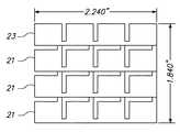
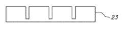
図5は、例示的な特定の一実施形態に基づくヒートシンク・ベース20の寸法入り上面図である。このヒートシンク・ベース20は、3つの第1の部分21と1つの第2の部分23とを含む。図6は、図5のヒートシンク・ベースの第1の部分21の寸法入り上面図である。図7は、図5のヒートシンク・ベースの第2の部分23の寸法入り上面図である。図5のヒートシンク・ベース20は、図5、図6および図7の寸法に従ってヒートシンク・ベース20を機械加工することにより、単一の材料片から形成することができる。代替として、図5のヒートシンク・ベース20を、3つの第1の部分21および1つの第2の部分23を別々に形成し、続いて部分21、23を図5に示すように(例えば溶接またはろう付けによって)接合することにより構築することもできる。 FIG. 5 is a dimensioned top view of the
図8は、マイクロプロセッサ(「プロセッサ」)の冷却用にヒートシンク10を含む電子デバイス50の側面図である。この例では、プロセッサが、システム・ボード60上の中央処理ユニット(CPU)62である。CPU62は、システム・ボード60上のソケット64内に配置されている。ヒートシンク・アセンブリ10をシステム・ボード60に固定する前に、ソケット64内にCPU62をゆるく配置する。ヒートシンク10は、ヒートシンク10のヒートシンク・ベース20とCPU62とをしっかりと係合させる従来の金具17、例えば接地されてない金属柱を使用して、取付けタブ16のところで固定される。これにより、CPU62が発生させた熱は、CPU62からヒートシンク10に伝達される。冷却フィン42を通る空気流を発生させて、ヒートシンク10を強制対流によって冷却するために、システム・ボード60にファン65が取り付けられる。これにより、ヒートシンクはCPU62を冷却する。 FIG. 8 is a side view of an
図9は、電子デバイス50の図8で強調した部分の拡大詳細図である。CPU62は、システム・ボード60の上を向いた表面上の対合電気接点68と整合した(ランド・グリッド・アレイなどの)電気接点66を有し、電気接点66は、CPU62がシステム・ボード60とインタフェースすることを可能にする。この例の金属層14は、システム・ボード60の接地層14である。CPUは、少なくとも1つの接地接点68Gに接地される。CPU62は、大量の電流を引き込むため、電子デバイス50内においてEMIを発生する可能性が高い。(CPUなどの)多くのICのコア周波数はしばしば、ヒートシンク・ベースおよび回路板の基準面によって形成される空洞の最初のいくつかの共振モードと同じ範囲にある。したがって、この場合、ヒートシンク・ベース20と金属接地層14との間の小さな間隙内において空洞共振効果が生じる可能性がある。従来のヒートシンクを使用すると、この空洞共振効果が、特定の共振周波数においてEMIを増幅する。しかしながら、金属接地層14と、ヒートシンク・ベース20の周期的パターンを有する態様は、一緒に、ある周波数のEMIを低減させる特性ストップバンドを有するEBG構造を形成する。前述のとおり、標的ストップバンドを達成するようにヒートシンク・ベースの物理パラメータを選択することによって、ストップバンドを調整することができる。標的ストップバンドは例えば、ピーク周波数を低減させるように選択することができる。 FIG. 9 is an enlarged detailed view of the part highlighted in FIG. 8 of the
図10は、周期的パターンを有する本発明の一実施形態に基づくヒートシンク・ベース20を使用した結果、従来の中実ヒートシンク・ベースに比べてEMIが低減したことを示すグラフ80である。グラフ80は、上曲線81を境界とする第1の周波数プロットと、下曲線82を境界とする第2の周波数プロットとを含む。上曲線81は、中実ヒートシンク・ベースを使用したある周波数範囲の周波数応答を表し、下曲線82は、周期的パターンを有するヒートシンク・ベースを使用した同じ周波数範囲の周波数応答を表す。原型ヒートシンク・ベースは厚さ0.25インチ(6.35mm)の銅製であり、それぞれ500ミル(12.7mm)×400ミル(10.2mm)のパッチの4×4アレイを有する。パッチを接続する枝は80ミル(2.03mm)×80ミル(2.03mm)とした。約4から5GHz、6から8GHzおよび10から16GHzの標的ストップバンド領域が示されている。周期的パターンを有するヒートシンク・ベースの幾何学的配列および物理パラメータを、この周波数範囲のピーク周波数を低減させるように選択した。グラフ80に明白に示されているように、周期的パターンを有するヒートシンク・ベースを使用した結果、従来のヒートシンク・ベースとは対照的に、ピーク周波数はかなり低い。周期的パターンを有するヒートシンク・ベースを使用すると、EMIの伝搬はかなり低減する。 FIG. 10 is a
図10の例では、ピーク周波数を低減させるように標的ストップバンドを選択した。しかしながら、所与のデバイスにおいて、プロセッサが発生させるピーク周波数が、他の回路と最も強く干渉する周波数であるとは限らない。したがって、全ての用途で、標的ストップバンドがピーク周波数を含む必要は必ずしもない。 In the example of FIG. 10, the target stopband was selected to reduce the peak frequency. However, in a given device, the peak frequency generated by the processor is not necessarily the frequency that most interferes with other circuits. Thus, for all applications, the target stopband need not necessarily include a peak frequency.
図11は、回路板上のプロセッサが発生させた電磁雑音の伝搬を低減させる本発明の一実施形態に基づく方法の概要を示す流れ図である。ステップ100は、プロセッサが発生させる電磁雑音の周波数帯を識別することを含む。選択する周波数帯は、プロセッサが発生させるピークEMI周波数、または回路板上の他のデバイス(特にアナログ・デバイス)の動作周波数、あるいはその両方を考慮して選択することができる。ステップ102は、識別した周波数帯内で標的ストップバンドを達成するように選択された幾何学的配列および物理パラメータを有する、間隔を置いて配置され、枝によって相互接続されたパッチの周期的パターンを選択することを含む。伝導性パッチのサイズ、形状および間隔はいずれも、ヒートシンク・ベースの周期的パターン構造によって達成される実際のストップバンドに影響を与える。周期的パターンを選択するこのステップは、パッチ幅、パッチ長、枝幅、枝長、ベース厚またはこれらの組合せを選択するステップを含むことができる。正方形のEBG構造(すなわちLP=WP)の物理寸法と第1の共振周波数の位置との間の一般的な関係は、下式によって与えられる。
上式で、A=WB+LPは、個々のEBG要素間の間隔と個々のEBG要素の寸法(すなわち幅または長さ)との和に対応する。ここで、c=3・108m/sであり、cは自由空間における光速を表し、εeffは、媒質の実効誘電率を表す。相互接続枝の寄与を考慮し、WP=LPおよびWB=LBであると仮定すると、この式は下式のように変形される。
長方形構造の場合には、EBGパッチの追加の長さおよびそれらの長さの組合せに対してLPを代入することによって、理論上、以降の他の全てのストップバンド位置を決定することができる。FIG. 11 is a flow diagram illustrating an overview of a method according to an embodiment of the present invention for reducing the propagation of electromagnetic noise generated by a processor on a circuit board. Step 100 includes identifying a frequency band of electromagnetic noise generated by the processor. The frequency band to be selected can be selected in consideration of the peak EMI frequency generated by the processor and / or the operating frequency of other devices (especially analog devices) on the circuit board. Step 102 creates a periodic pattern of spaced patches, interconnected by branches, having a geometrical arrangement and physical parameters selected to achieve a target stopband within the identified frequency band. Including selecting. The size, shape and spacing of the conductive patches all affect the actual stopband achieved by the heat sink based periodic pattern structure. This step of selecting the periodic pattern can include selecting a patch width, patch length, branch width, branch length, base thickness, or a combination thereof. The general relationship between the physical dimensions of a square EBG structure (ie LP = WP ) and the position of the first resonance frequency is given by:
In the above equation,A = W B +L P corresponds to the sum of the dimensions of the gap and the individual EBG elements between individual EBG elements (i.e. width or length). Here, c = 3 · 108 m / s, c represents the speed of light in free space, and εeff represents the effective dielectric constant of the medium. Assuming WP = LP and WB = LB taking into account the contribution of the interconnecting branches, this equation is transformed as:
In the case of a rectangular structure, all other subsequent stopband positions can theoretically be determined by substituting LP for additional lengths of EBG patches and combinations of those lengths. .
ステップ104では、ステップ102で選択した周期的パターンに従って、ヒートシンク・ベースを形成することができる。ステップ106では、連続する電気伝導性層を有する回路板を選択する。形成されたこの層は、積層回路板の接地面、電源面などの金属層とすることができる。回路板は一般に、プロセッサ、ならびに他のディジタル回路またはアナログ回路あるいはその両方を含む。ステップ108では、周期的パターンを有するヒートシンク・ベースを、プロセッサと熱接触するように固定する。周期的パターンを有するヒートシンク・ベースと金属層は、一緒に、選択したストップバンド周波数範囲におけるEMIの振幅を低減させるEBG構造を形成する。 In
本明細書で使用される用語は、特定の実施形態を記述することだけを目的としたものであり、本発明を限定することは意図されていない。本明細書で使用されるとき、単数形「a」「an」および「the」は、そうでないことが文脈から明らかである場合を除き、複数形も含むことが意図されている。また、本明細書で使用されるとき、用語「含む」は、明示された特徴、完全体、ステップ、動作、要素、構成要素またはグループ、あるいはこれらの任意の組合せの存在を指定するが、1つまたは複数の他の特徴、完全体、ステップ、動作、要素、構成要素またはこれらのグループ、あるいはこれらの任意の組合せの存在または追加を排除しないことが理解される。用語「好ましくは」、「好ましい」、「任意選択で」、「できる」および同種の用語は、言及されている項目、条件またはステップが、本発明の任意選択の特徴(必須でない特徴)であることを示すのに使用される。 The terminology used herein is for the purpose of describing particular embodiments only and is not intended to be limiting of the invention. As used herein, the singular forms “a”, “an”, and “the” are intended to include the plural forms as well, unless otherwise apparent from the context. Also, as used herein, the term “comprising” specifies the presence of a specified feature, completeness, step, action, element, component or group, or any combination thereof, It is understood that the presence or addition of one or more other features, completeness, steps, actions, elements, components or groups thereof, or any combination thereof is not excluded. The terms “preferably”, “preferred”, “optional”, “can” and like terms refer to an optional feature (non-essential feature) of the item, condition or step referred to. Used to indicate that
下記の特許請求の範囲に記載された全ての手段またはステップならびに機能要素の対応する構造、材料、作用および等価物は、特許請求の範囲に特に記載された他の請求の要素と組み合わせて機能を実行する任意の構造、材料または作用を含むことが意図されている。本発明の説明は、例示および説明のために示したものだが、網羅的であること、または開示された形態に本発明を限定することは意図されていない。本発明の範囲および趣旨を逸脱しない多くの修正および変更が当業者には明白であろう。この実施形態は、本発明の原理および実際な用途を最もよく説明するため、および、当業者が、企図された特定の用途に適合したさまざまな変更を有するさまざまな実施形態に関して、本発明を理解することを可能にするために、選び出し、説明した。 All means or steps recited in the claims below and the corresponding structures, materials, acts and equivalents of the functional elements function in combination with other claimed elements specifically recited in the claims. It is intended to include any structure, material or action to be performed. The description of the present invention has been presented for purposes of illustration and description, but is not intended to be exhaustive or limited to the invention in the form disclosed. Many modifications and variations will be apparent to those skilled in the art without departing from the scope and spirit of the invention. This embodiment is intended to best explain the principles and practical applications of the present invention, and for those skilled in the art to understand the present invention with respect to various embodiments having various modifications adapted to the particular application contemplated. Selected and explained to make it possible to do.
10 ヒートシンク
14 金属層、連続する電気伝導性の回路板層、接地層、金属接地層
16 取付けタブ
17 金具
20 ヒートシンク・ベース
21 ヒートシンク・ベースの第1の部分
22 ヒートシンク・ベースの第1の表面、ヒートシンク・ベースの上面
23 ヒートシンク・ベースの第2の部分
24 ヒートシンク・ベースの第2の表面、ヒートシンク・ベースの下面
25 周期的パターン構造の断面
26 熱伝導性/非電気伝導性結合材
28 パッチ(patch)
29 開口部
30 枝(branch)
31 L字形スロット
32 オープン・スロット32
33 ヒートシンク・ベースの外縁
34 熱伝導性/非電気伝導性充填材
40 冷却フィン構造
42 冷却フィン、ヒートシンク・フィン
50 電子デバイス
60 システム・ボード
62 中央処理ユニット(CPU)
64 システム・ボード上のソケット
65 ファン
66 電気接点
68 対合電気接点
68G 接地接点
80 グラフ
81 上曲線
82 下曲線10
29
31 L-shaped slot 32 Open slot 32
33 Outer edge of
64 Socket on
Claims (20)
Translated fromJapanese前記パッチを構造的に接続する複数の枝であり、各枝が、隣接するパッチを接続し、前記基準面内において、隣接するそれぞれのパッチの幅よりも狭い幅を有する、複数の枝と、
前記ベースに結合され、前記基準面に垂直に延びる、複数の熱伝導性冷却フィンと
を含むヒートシンク。A base having a periodic pattern structure including an array of electrically conductive / thermally conductive patches spaced in two dimensions of a reference plane and having a thickness perpendicular to the reference plane;
A plurality of branches structurally connecting the patches, each branch connecting adjacent patches and having a width narrower than the width of each adjacent patch in the reference plane;
A heat sink, comprising: a plurality of thermally conductive cooling fins coupled to the base and extending perpendicular to the reference surface.
をさらに含む、請求項1に記載のヒートシンク。The heat sink of claim 1, further comprising a thermally conductive / non-electrically conductive filler that fills a space between the adjacent patches.
をさらに含む、請求項1に記載のヒートシンク。The heat sink of claim 1, further comprising a thermally conductive / non-electrically conductive binder that couples the cooling fin to a surface of the base.
前記プリント回路板に物理的に結合され、前記電気伝導性層に電気的に結合された、プロセッサと、
前記プロセッサと熱接触するように前記回路板に結合された、ヒートシンクと
を含み、
前記ヒートシンクが、前記伝導性層に平行に間隔を置いて配置され、前記伝導性層に垂直な厚さを有する電気伝導性/熱伝導性パッチのアレイを含む周期的パターン構造を有するベースと、前記パッチを構造的に接続する複数の枝であり、各枝が、隣接する2つのパッチ間の開口部を横切って延び、基準面内において、隣接するそれぞれのパッチの幅よりも狭い幅を有する、複数の枝と、前記ベースに結合され、前記基準面に垂直に延びる複数の熱伝導性冷却フィンとを含む
装置。A printed circuit board comprising a continuous electrically conductive layer;
A processor physically coupled to the printed circuit board and electrically coupled to the electrically conductive layer;
A heat sink coupled to the circuit board in thermal contact with the processor;
A base having a periodic pattern structure including an array of electrically conductive / thermally conductive patches, wherein the heat sink is spaced parallel to the conductive layer and has a thickness perpendicular to the conductive layer; A plurality of branches structurally connecting the patches, each branch extending across an opening between two adjacent patches, and having a width narrower than a width of each adjacent patch in a reference plane A plurality of branches and a plurality of thermally conductive cooling fins coupled to the base and extending perpendicular to the reference plane.
請求項10に記載の装置。A plurality of metal pillars for fixing the processor to the circuit board, wherein the metal pillars are not grounded to a ground layer;
The apparatus according to claim 10.
をさらに含む、請求項9に記載の装置。The apparatus of claim 9, further comprising a thermally / non-electrically conductive filler that fills a space between the adjacent patches.
前記集積回路が発生させる前記電磁雑音の周波数帯を識別するステップと、
前記識別した周波数帯内にストップバンドを有する幾何学的配列を有する、間隔を置いて配置され、枝によって相互接続されたパッチの周期的パターンを選択するステップと、
前記集積回路を、前記選択した周期的パターンを有する電気伝導性/熱伝導性材料を含むベースを有するヒートシンクと熱接触させるステップと
を含む方法。A method for reducing propagation of electromagnetic noise generated by an integrated circuit, comprising:
Identifying a frequency band of the electromagnetic noise generated by the integrated circuit;
Selecting a periodic pattern of spaced patches, interconnected by branches, having a geometric arrangement having stop bands within the identified frequency bands;
Thermally contacting the integrated circuit with a heat sink having a base comprising an electrically conductive / thermally conductive material having the selected periodic pattern.
Applications Claiming Priority (2)
| Application Number | Priority Date | Filing Date | Title |
|---|---|---|---|
| US12/536655 | 2009-08-06 | ||
| US12/536,655US7848108B1 (en) | 2009-08-06 | 2009-08-06 | Heatsink with periodically patterned baseplate structure |
Related Child Applications (1)
| Application Number | Title | Priority Date | Filing Date |
|---|---|---|---|
| JP2015039193ADivisionJP5914717B2 (en) | 2009-08-06 | 2015-02-27 | Heat sink including a base plate structure having a periodic pattern, and related apparatus and method (heat sink including a base plate structure having a periodic pattern) |
Publications (2)
| Publication Number | Publication Date |
|---|---|
| JP2011040742Atrue JP2011040742A (en) | 2011-02-24 |
| JP5765897B2 JP5765897B2 (en) | 2015-08-19 |
Family
ID=43244135
Family Applications (2)
| Application Number | Title | Priority Date | Filing Date |
|---|---|---|---|
| JP2010174276AActiveJP5765897B2 (en) | 2009-08-06 | 2010-08-03 | Heat sink including a base plate structure having a periodic pattern, and related apparatus and method (heat sink including a base plate structure having a periodic pattern) |
| JP2015039193AActiveJP5914717B2 (en) | 2009-08-06 | 2015-02-27 | Heat sink including a base plate structure having a periodic pattern, and related apparatus and method (heat sink including a base plate structure having a periodic pattern) |
Family Applications After (1)
| Application Number | Title | Priority Date | Filing Date |
|---|---|---|---|
| JP2015039193AActiveJP5914717B2 (en) | 2009-08-06 | 2015-02-27 | Heat sink including a base plate structure having a periodic pattern, and related apparatus and method (heat sink including a base plate structure having a periodic pattern) |
Country Status (5)
| Country | Link |
|---|---|
| US (1) | US7848108B1 (en) |
| JP (2) | JP5765897B2 (en) |
| KR (1) | KR20110014956A (en) |
| CN (1) | CN101996963B (en) |
| TW (1) | TWI440425B (en) |
Cited By (3)
| Publication number | Priority date | Publication date | Assignee | Title |
|---|---|---|---|---|
| WO2012169104A1 (en)* | 2011-06-10 | 2012-12-13 | 日本電気株式会社 | Electronic device, structure, and heat sink |
| JP2014027180A (en)* | 2012-07-27 | 2014-02-06 | Toshiba Corp | Electronic circuit and semiconductor component |
| WO2023032247A1 (en)* | 2021-09-02 | 2023-03-09 | 日本電気株式会社 | Wireless device, wireless system, and heat dissipation structure |
Families Citing this family (19)
| Publication number | Priority date | Publication date | Assignee | Title |
|---|---|---|---|---|
| KR20120000282A (en)* | 2010-06-25 | 2012-01-02 | 삼성전자주식회사 | Heat spreader and semiconductor package including the same |
| US10403973B2 (en)* | 2014-04-22 | 2019-09-03 | Intel Corporation | EBG designs for mitigating radio frequency interference |
| EP3278361A4 (en)* | 2015-07-31 | 2019-02-20 | Hewlett-Packard Enterprise Development LP | Multi-chip module |
| US20170214150A1 (en) | 2016-01-25 | 2017-07-27 | Philips Lighting Holding B.V. | Apparatus comprising antenna and heat sink |
| US20170347490A1 (en)* | 2016-05-24 | 2017-11-30 | Texas Instruments Incorporated | High-frequency antenna structure with high thermal conductivity and high surface area |
| US10553930B2 (en)* | 2016-12-30 | 2020-02-04 | Symantec Corporation | Antenna system for wireless communication devices and other wireless applications |
| DE102017200121A1 (en)* | 2017-01-05 | 2018-07-05 | Fraunhofer-Gesellschaft zur Förderung der angewandten Forschung e.V. | Wafer Level Package with at least one integrated antenna element |
| DE102017200122B4 (en) | 2017-01-05 | 2020-07-23 | Fraunhofer-Gesellschaft zur Förderung der angewandten Forschung e.V. | Wafer level package with integrated antennas and means for shielding, system for this and method for its production |
| DE102017200124A1 (en) | 2017-01-05 | 2018-07-05 | Fraunhofer-Gesellschaft zur Förderung der angewandten Forschung e.V. | Wafer Level Packages with integrated or embedded antenna |
| KR102658311B1 (en)* | 2017-02-08 | 2024-04-18 | 삼성전자주식회사 | the Electronic Device including the Speaker |
| CN107240770B (en)* | 2017-05-10 | 2019-11-26 | 哈尔滨工程大学 | A kind of periodic spatial wave resistance gear decoupling arrangements for micro-strip antenna array |
| DE202019005902U1 (en)* | 2018-08-21 | 2023-04-11 | Laird Technologies, Inc. | Patterned materials and foils as well as systems |
| CN108909113B (en)* | 2018-08-24 | 2024-09-24 | 深圳市飞鸿达科技有限公司 | Heat conduction electromagnetic noise suppression sheet and preparation method thereof |
| KR102326231B1 (en)* | 2019-04-23 | 2021-11-16 | 미쓰비시덴키 가부시키가이샤 | Electronics |
| KR102290036B1 (en)* | 2019-05-15 | 2021-08-18 | 주식회사 케이엠더블유 | Antenna apparatus |
| US20220117112A1 (en)* | 2020-10-12 | 2022-04-14 | Intel Corporation | Enhanced electronic package thermal dissipation with in-situ transpiration cooling and reduced thermal interstitial resistance |
| US11252841B1 (en)* | 2021-02-18 | 2022-02-15 | Giftedness And Creativity Company | Heat sink with slotted pin fins |
| CN113611678A (en)* | 2021-08-30 | 2021-11-05 | 江西江南精密科技有限公司 | A kind of high-efficiency and precise heat-dissipating copper block and manufacturing process |
| CN116234323A (en)* | 2022-07-01 | 2023-06-06 | 北京超弦存储器研究院 | Three-dimensional stacked chip and electronic device |
Citations (6)
| Publication number | Priority date | Publication date | Assignee | Title |
|---|---|---|---|---|
| JPS6381838A (en)* | 1986-09-25 | 1988-04-12 | Hitachi Cable Ltd | Cooling element and manufacture thereof |
| JPH0278255A (en)* | 1988-09-14 | 1990-03-19 | Hitachi Ltd | Resin-encapsulated semiconductor device |
| JP2000156578A (en)* | 1998-11-20 | 2000-06-06 | Nec Corp | Heat dissipating structure for electronic apparatus |
| JP2007273943A (en)* | 2006-03-30 | 2007-10-18 | General Electric Co <Ge> | Advanced heat sink and thermal spreader |
| JP2008010859A (en)* | 2006-06-02 | 2008-01-17 | Renesas Technology Corp | Semiconductor device |
| JP2008109161A (en)* | 2008-01-11 | 2008-05-08 | Fujitsu Ltd | Board unit |
Family Cites Families (12)
| Publication number | Priority date | Publication date | Assignee | Title |
|---|---|---|---|---|
| US6437438B1 (en)* | 2000-06-30 | 2002-08-20 | Intel Corporation | Eddy current limiting thermal plate |
| US6563198B1 (en)* | 2001-08-01 | 2003-05-13 | Lsi Logic Corporation | Adhesive pad having EMC shielding characteristics |
| JP2003298283A (en)* | 2002-03-28 | 2003-10-17 | Seiko Epson Corp | Electromagnetic wave shielding member, recording device |
| TWM241965U (en)* | 2003-05-23 | 2004-08-21 | Hon Hai Prec Ind Co Ltd | EMI-Attenuating air ventilation panel |
| US7748440B2 (en)* | 2004-06-01 | 2010-07-06 | International Business Machines Corporation | Patterned structure for a thermal interface |
| JP4843611B2 (en) | 2004-10-01 | 2011-12-21 | デ,ロシェモント,エル.,ピエール | Ceramic antenna module and manufacturing method thereof |
| CN1845666A (en)* | 2005-04-07 | 2006-10-11 | 华硕电脑股份有限公司 | shelter structure |
| WO2006132957A2 (en) | 2005-06-07 | 2006-12-14 | University Of Florida Research Foundation, Inc. | Integrated electronic circuitry and heat sink |
| CN101026132A (en)* | 2006-02-22 | 2007-08-29 | 特奕展科技股份有限公司 | Multi-mode heat sink including cooling chip and heat dissipation method thereof |
| JP2007235460A (en) | 2006-02-28 | 2007-09-13 | Mitsumi Electric Co Ltd | Antenna system |
| CN101031197A (en)* | 2006-03-02 | 2007-09-05 | 华硕电脑股份有限公司 | Electronic device with electromagnetic interference suppression function and heat dissipation component thereof |
| US7839654B2 (en)* | 2007-02-28 | 2010-11-23 | International Business Machines Corporation | Method for ultimate noise isolation in high-speed digital systems on packages and printed circuit boards (PCBS) |
- 2009
- 2009-08-06USUS12/536,655patent/US7848108B1/enactiveActive
- 2010
- 2010-06-10TWTW099118846Apatent/TWI440425B/enactive
- 2010-07-21KRKR1020100070464Apatent/KR20110014956A/ennot_activeCeased
- 2010-08-03JPJP2010174276Apatent/JP5765897B2/enactiveActive
- 2010-08-06CNCN2010102490562Apatent/CN101996963B/ennot_activeExpired - Fee Related
- 2015
- 2015-02-27JPJP2015039193Apatent/JP5914717B2/enactiveActive
Patent Citations (6)
| Publication number | Priority date | Publication date | Assignee | Title |
|---|---|---|---|---|
| JPS6381838A (en)* | 1986-09-25 | 1988-04-12 | Hitachi Cable Ltd | Cooling element and manufacture thereof |
| JPH0278255A (en)* | 1988-09-14 | 1990-03-19 | Hitachi Ltd | Resin-encapsulated semiconductor device |
| JP2000156578A (en)* | 1998-11-20 | 2000-06-06 | Nec Corp | Heat dissipating structure for electronic apparatus |
| JP2007273943A (en)* | 2006-03-30 | 2007-10-18 | General Electric Co <Ge> | Advanced heat sink and thermal spreader |
| JP2008010859A (en)* | 2006-06-02 | 2008-01-17 | Renesas Technology Corp | Semiconductor device |
| JP2008109161A (en)* | 2008-01-11 | 2008-05-08 | Fujitsu Ltd | Board unit |
Cited By (5)
| Publication number | Priority date | Publication date | Assignee | Title |
|---|---|---|---|---|
| WO2012169104A1 (en)* | 2011-06-10 | 2012-12-13 | 日本電気株式会社 | Electronic device, structure, and heat sink |
| US9629282B2 (en) | 2011-06-10 | 2017-04-18 | Nec Corporation | Electronic device, structure, and heat sink |
| JP2014027180A (en)* | 2012-07-27 | 2014-02-06 | Toshiba Corp | Electronic circuit and semiconductor component |
| US9406622B2 (en) | 2012-07-27 | 2016-08-02 | Kabushiki Kaisha Toshiba | Electronic circuit and semiconductor component |
| WO2023032247A1 (en)* | 2021-09-02 | 2023-03-09 | 日本電気株式会社 | Wireless device, wireless system, and heat dissipation structure |
Also Published As
| Publication number | Publication date |
|---|---|
| TW201112938A (en) | 2011-04-01 |
| JP2015135979A (en) | 2015-07-27 |
| KR20110014956A (en) | 2011-02-14 |
| US7848108B1 (en) | 2010-12-07 |
| JP5914717B2 (en) | 2016-05-11 |
| TWI440425B (en) | 2014-06-01 |
| CN101996963B (en) | 2013-01-30 |
| CN101996963A (en) | 2011-03-30 |
| JP5765897B2 (en) | 2015-08-19 |
Similar Documents
| Publication | Publication Date | Title |
|---|---|---|
| JP5914717B2 (en) | Heat sink including a base plate structure having a periodic pattern, and related apparatus and method (heat sink including a base plate structure having a periodic pattern) | |
| US10130003B2 (en) | Reduced thermal transfer to Peltier cooled FETs | |
| US6956285B2 (en) | EMI grounding pins for CPU/ASIC chips | |
| US6943436B2 (en) | EMI heatspreader/lid for integrated circuit packages | |
| KR100609204B1 (en) | Electrical components and electrical circuit modules with connected ground planes | |
| EP3065167B1 (en) | High-frequency module and microwave transceiver | |
| KR101008772B1 (en) | Integrated circuit devices, electronic circuit support boards and thermal connections between integrated circuits and heat sinks | |
| KR20160120486A (en) | Circuit board and method of manufacturing the same | |
| JPH06252282A (en) | Shield structure of package | |
| JP2015535392A (en) | Thermally conductive element and method for forming the thermally conductive element | |
| CN101667560B (en) | Electronic device and method for coping with electrostatic discharge | |
| RU2489770C1 (en) | Hybrid microwave-frequency integrated circuit | |
| JP4958189B2 (en) | Integrated circuit mounting structure | |
| JPWO2008035540A1 (en) | Electronic device-equipped equipment and its resonance suppression method | |
| JPH1117083A (en) | Radiator device with anti-emi function | |
| KR20050025714A (en) | Single-body type eletro-device case | |
| KR101940295B1 (en) | Board structure with radio frequency wave shield | |
| CN215735631U (en) | Electromagnetic shielding structure, radio frequency device and base station | |
| CN215379561U (en) | Metal radiator and electronic control unit comprising same | |
| JPH07142832A (en) | Printed board and electronic circuit employing the same | |
| KR101305581B1 (en) | Shield member and pcb comprising the shield member | |
| JP2011249374A (en) | Electronic apparatus | |
| JPH03177095A (en) | Method of dissipating heat of electronic component | |
| Bhobe et al. | A study of grounded-heatspreader for EMI mitigation of ASIC IC package | |
| JPH05167204A (en) | Printed board |
Legal Events
| Date | Code | Title | Description |
|---|---|---|---|
| A621 | Written request for application examination | Free format text:JAPANESE INTERMEDIATE CODE: A621 Effective date:20130404 | |
| A977 | Report on retrieval | Free format text:JAPANESE INTERMEDIATE CODE: A971007 Effective date:20140314 | |
| A131 | Notification of reasons for refusal | Free format text:JAPANESE INTERMEDIATE CODE: A131 Effective date:20140401 | |
| A02 | Decision of refusal | Free format text:JAPANESE INTERMEDIATE CODE: A02 Effective date:20141104 | |
| RD12 | Notification of acceptance of power of sub attorney | Free format text:JAPANESE INTERMEDIATE CODE: A7432 Effective date:20141125 | |
| A521 | Request for written amendment filed | Free format text:JAPANESE INTERMEDIATE CODE: A821 Effective date:20141126 | |
| A521 | Request for written amendment filed | Free format text:JAPANESE INTERMEDIATE CODE: A523 Effective date:20150227 | |
| A911 | Transfer to examiner for re-examination before appeal (zenchi) | Free format text:JAPANESE INTERMEDIATE CODE: A911 Effective date:20150310 | |
| TRDD | Decision of grant or rejection written | ||
| A01 | Written decision to grant a patent or to grant a registration (utility model) | Free format text:JAPANESE INTERMEDIATE CODE: A01 Effective date:20150519 | |
| A61 | First payment of annual fees (during grant procedure) | Free format text:JAPANESE INTERMEDIATE CODE: A61 Effective date:20150616 | |
| R150 | Certificate of patent or registration of utility model | Ref document number:5765897 Country of ref document:JP Free format text:JAPANESE INTERMEDIATE CODE: R150 | |
| S111 | Request for change of ownership or part of ownership | Free format text:JAPANESE INTERMEDIATE CODE: R313113 | |
| R350 | Written notification of registration of transfer | Free format text:JAPANESE INTERMEDIATE CODE: R350 | |
| R250 | Receipt of annual fees | Free format text:JAPANESE INTERMEDIATE CODE: R250 | |
| R250 | Receipt of annual fees | Free format text:JAPANESE INTERMEDIATE CODE: R250 | |
| S111 | Request for change of ownership or part of ownership | Free format text:JAPANESE INTERMEDIATE CODE: R313113 | |
| R360 | Written notification for declining of transfer of rights | Free format text:JAPANESE INTERMEDIATE CODE: R360 | |
| R360 | Written notification for declining of transfer of rights | Free format text:JAPANESE INTERMEDIATE CODE: R360 | |
| R371 | Transfer withdrawn | Free format text:JAPANESE INTERMEDIATE CODE: R371 | |
| S111 | Request for change of ownership or part of ownership | Free format text:JAPANESE INTERMEDIATE CODE: R313113 | |
| R350 | Written notification of registration of transfer | Free format text:JAPANESE INTERMEDIATE CODE: R350 | |
| R250 | Receipt of annual fees | Free format text:JAPANESE INTERMEDIATE CODE: R250 | |
| R250 | Receipt of annual fees | Free format text:JAPANESE INTERMEDIATE CODE: R250 | |
| R250 | Receipt of annual fees | Free format text:JAPANESE INTERMEDIATE CODE: R250 | |
| R250 | Receipt of annual fees | Free format text:JAPANESE INTERMEDIATE CODE: R250 | |
| R250 | Receipt of annual fees | Free format text:JAPANESE INTERMEDIATE CODE: R250 | |
| S111 | Request for change of ownership or part of ownership | Free format text:JAPANESE INTERMEDIATE CODE: R313113 | |
| R350 | Written notification of registration of transfer | Free format text:JAPANESE INTERMEDIATE CODE: R350 | |
| R250 | Receipt of annual fees | Free format text:JAPANESE INTERMEDIATE CODE: R250 |