Movatterモバイル変換


[0]ホーム

URL:


JP2011029089A - Illumination fixture - Google Patents

Illumination fixture
Download PDF

Info

Publication number
JP2011029089A
JP2011029089AJP2009175856AJP2009175856AJP2011029089AJP 2011029089 AJP2011029089 AJP 2011029089AJP 2009175856 AJP2009175856 AJP 2009175856AJP 2009175856 AJP2009175856 AJP 2009175856AJP 2011029089 AJP2011029089 AJP 2011029089A
Authority
JP
Japan
Prior art keywords
light emitting
functional element
light
unit
mounting substrate
Prior art date
Legal status (The legal status is an assumption and is not a legal conclusion. Google has not performed a legal analysis and makes no representation as to the accuracy of the status listed.)
Withdrawn
Application number
JP2009175856A
Other languages
Japanese (ja)
Inventor
Ken Ichioka
一岡  建
Atsushi Otsubo
篤 大坪
Shinichi Nagaoka
慎一 長岡
Tadahiro Kono
忠博 河野
Current Assignee (The listed assignees may be inaccurate. Google has not performed a legal analysis and makes no representation or warranty as to the accuracy of the list.)
Panasonic Electric Works Co Ltd
Original Assignee
Panasonic Electric Works Co Ltd
Priority date (The priority date is an assumption and is not a legal conclusion. Google has not performed a legal analysis and makes no representation as to the accuracy of the date listed.)
Filing date
Publication date
Application filed by Panasonic Electric Works Co LtdfiledCriticalPanasonic Electric Works Co Ltd
Priority to JP2009175856ApriorityCriticalpatent/JP2011029089A/en
Priority to CN201010243134.8Aprioritypatent/CN101986005B/en
Publication of JP2011029089ApublicationCriticalpatent/JP2011029089A/en
Withdrawnlegal-statusCriticalCurrent

Links

Images

Landscapes

Abstract

Translated fromJapanese

【課題】所定の機能を有する機能素子部の温度上昇を抑制しつつ、均一な配光分布を得ることができるとともに光出力の低下を抑制することができる照明器具を提供する。
【解決手段】照明器具は、LEDチップ(図示せず)を用いた複数の発光部2と、センサ部(機能素子部)3の出力に基づいて発光部2への供給電力を制御することにより発光部2を点灯および消灯させる制御回路部(制御手段)43を有する点灯装置(図示せず)と、円板状に形成され且つセンサ部3が挿通可能なセンサ部挿通孔(機能素子部挿通孔)1bが貫設されたベース基板1と、センサ部3が取着され且つセンサ部3をセンサ部挿通孔1bに挿通する形でベース基板1の他表面側に配置されるセンサ部取付基板(機能素子部取付基板)201とを備える。センサ部取付基板201が、センサ部3におけるベース基板1の前記一表面側に突出した部分が各発光部2の光を遮らないように配置されている。
【選択図】図1
Provided is a lighting apparatus capable of obtaining a uniform light distribution while suppressing a decrease in light output while suppressing an increase in temperature of a functional element portion having a predetermined function.
A lighting apparatus controls power supplied to a light emitting unit 2 based on outputs of a plurality of light emitting units 2 using LED chips (not shown) and a sensor unit (functional element unit) 3. A lighting device (not shown) having a control circuit unit (control means) 43 for turning on and off the light emitting unit 2 and a sensor unit insertion hole (functional element unit insertion) formed in a disk shape and into which the sensor unit 3 can be inserted Hole) 1b through which the base substrate 1 and the sensor unit 3 are attached and the sensor unit mounting substrate is disposed on the other surface side of the base substrate 1 in such a manner that the sensor unit 3 is inserted into the sensor unit insertion hole 1b. (Functional element portion mounting substrate) 201. The sensor unit mounting substrate 201 is arranged so that the portion of the sensor unit 3 protruding to the one surface side of the base substrate 1 does not block the light of each light emitting unit 2.
[Selection] Figure 1

Description

Translated fromJapanese

本発明は、LEDチップを用いた発光部を備えた照明器具に関するものである。  The present invention relates to a lighting apparatus including a light emitting unit using an LED chip.

従来、照明器具の光源としては、白熱灯や蛍光灯が多く使用されていたが、近年では、高出力のLEDチップを用いた白色光源が開発され、当該高出力のLEDチップを用いた白色光源からなる発光部と、当該発光部に電流を出力することにより当該発光部を点灯させる点灯装置を備えた照明器具が増加してきている。  Conventionally, incandescent lamps and fluorescent lamps have been often used as light sources for lighting fixtures, but in recent years, white light sources using high-power LED chips have been developed, and white light sources using such high-power LED chips. There are an increasing number of luminaires including a light emitting unit including the above and a lighting device that turns on the light emitting unit by outputting a current to the light emitting unit.

ここに、LEDチップを用いた白色光源は、高出力になるほど発熱量が大きくなる。従って、高出力のLEDチップを用いた白色光源からなる発光部を備えた照明器具では、当該発光部および当該発光部の周辺に配置された部品の温度上昇を抑制するための放熱手段が必要となる。  Here, the amount of heat generated from the white light source using the LED chip increases as the output increases. Therefore, in a lighting fixture including a light emitting unit composed of a white light source using a high-power LED chip, a heat dissipating unit is required to suppress the temperature rise of the light emitting unit and components arranged around the light emitting unit. Become.

一方、照明器具本体に設けられた手動のスイッチを操作することにより点灯装置を制御して発光部を点灯および消灯させることができる照明器具の他に、リモートコントローラを操作することによりリモートコントローラから送信される無線信号に基づいて点灯装置から発光部への電流出力を制御して発光部を点灯および消灯させることができる制御手段を備えた照明器具や、人の存在の有無を検知する赤外線センサ素子や周囲の明るさを検知する明るさセンサの出力に基づいて点灯装置から発光部への電流出力を制御して発光部を点灯および消灯させる制御手段を備えた照明器具が提案されている。ここで、リモートコントローラから送信される無線信号に基づいて点灯装置から発光部への電流出力を制御する制御手段を備えた照明器具では、リモートコントローラから送信される無線信号を受信するための機能素子である信号受信用素子を設ける必要があり、赤外線センサ素子の出力に基づいて点灯装置から発光部への電流出力を制御する制御手段を備えた照明器具では、機能素子である赤外線センサ素子を設ける必要がある。ここで、前記信号受信用素子や前記赤外線センサ素子は、一般的に耐熱性の低いものが多く、高出力のLEDチップを用いた発光部を備えた照明器具の場合、前記信号受信用素子や前記赤外線センサ素子の温度上昇に注意する必要がある。  On the other hand, in addition to the lighting fixtures that can turn on and off the light-emitting unit by controlling the lighting device by operating a manual switch provided on the lighting fixture body, send from the remote controller by operating the remote controller Luminaire with control means capable of turning on and off the light emitting unit by controlling the current output from the lighting device to the light emitting unit based on the wireless signal to be emitted, and an infrared sensor element for detecting the presence or absence of a person In addition, there has been proposed a lighting apparatus including a control unit that controls the current output from the lighting device to the light emitting unit based on the output of a brightness sensor that detects ambient brightness and turns on and off the light emitting unit. Here, in the lighting fixture provided with the control means which controls the electric current output from a lighting device to a light emission part based on the radio signal transmitted from a remote controller, the functional element for receiving the radio signal transmitted from a remote controller It is necessary to provide a signal receiving element, and in a lighting fixture provided with control means for controlling the current output from the lighting device to the light emitting unit based on the output of the infrared sensor element, the infrared sensor element which is a functional element is provided. There is a need. Here, the signal receiving element and the infrared sensor element are generally low in heat resistance, and in the case of a lighting fixture having a light emitting unit using a high-power LED chip, the signal receiving element or It is necessary to pay attention to the temperature rise of the infrared sensor element.

前記信号受信用素子や前記赤外線センサ素子等の機能素子の温度上昇を抑制するためには、前記機能素子を発熱量の大きい前記発光部から離れた場所に配置するのが効果的である。ところが、この場合、照明器具が大型化したり、デザイン性の低下を招く等のおそれがある。  In order to suppress the temperature rise of the functional elements such as the signal receiving element and the infrared sensor element, it is effective to dispose the functional element in a place away from the light emitting part that generates a large amount of heat. However, in this case, there is a risk that the lighting fixture will be enlarged or the design will be degraded.

これに対して、従来から、図6に示すように、LEDチップを用いた複数の発光部2’と、当該複数の発光部2’が実装されるとともに当該複数の発光部2’を直列に接続するための回路パターン(図示せず)が形成された回路基板51’と、人感センサや明るさセンサ等からなるセンサ部3’と、センサ部3’およびセンサ部3’からの出力に基づいて後述の電源回路を制御するための制御回路(図示せず)が設けられた制御基板52’と、円板状に形成され且つ一表面側に回路基板51’が取着されるとともに他表面側に制御基板52’が取着されたベース基板1’と、ベース基板1’の前記他表面側に配置され且つ回路基板51’および制御基板52’それぞれがリード線7’を介して接続され発光部2’に電力を供給する電源回路(図示せず)が設けられた電源基板53’と、外形が電球状に形成され且つ回路基板51’および制御基板52’が取着されたベース基板1’を前記一表面側を発光部2’からの光が出射する方向に向けた形で支持するとともに電源基板53’をベース基板1’の前記他表面側に配置される形で支持する器具本体10’とを備え、前記制御回路が、センサ部3’の出力に基づいて前記電源回路の出力を制御して前記電源回路から回路基板51’への電流の供給および停止を行うことで、複数の発光部2’を点灯および消灯させる照明器具が提案されている(特許文献1参照)。ここにおいて、前記点灯回路、前記制御回路および前記電源回路から点灯装置が構成されている。なお、前記人感センサとしては、例えば、人体から放射される赤外線を検知する機能素子である赤外線センサ素子を用いた赤外線センサがある。また、前記明るさセンサとしては、可視光の受光強度に応じて電圧を出力する機能素子である受光素子を用いて照明器具の周囲の明るさを検知する照度センサがある。  In contrast, conventionally, as shown in FIG. 6, a plurality oflight emitting units 2 ′ using LED chips and the plurality oflight emitting units 2 ′ are mounted and the plurality oflight emitting units 2 ′ are connected in series. A circuit board 51 ′ on which a circuit pattern (not shown) for connection is formed, asensor unit 3 ′ composed of a human sensor, a brightness sensor, and the like, and outputs from thesensor unit 3 ′ and thesensor unit 3 ′ Acontrol board 52 ′ provided with a control circuit (not shown) for controlling a power supply circuit, which will be described later, and a circuit board 51 ′ formed in a disk shape and attached to one surface side and the otherA base substrate 1 ′ having acontrol board 52 ′ attached to the front surface side, and arranged on the other surface side of thebase substrate 1 ′ and connected to the circuit board 51 ′ and thecontrol board 52 ′ via lead wires 7 ′. Power supply circuit for supplying power to thelight emitting section 2 ′ ( (Not shown) and abase substrate 1 ′ having an outer shape formed in a light bulb shape and having a circuit board 51 ′ and acontrol board 52 ′ attached to thelight emitting portion 2 ′. And aninstrument body 10 ′ for supporting thepower supply board 53 ′ in a form arranged on the other surface side of thebase substrate 1 ′, and supporting thepower supply board 53 ′ in the direction in which the light is emitted. A lighting fixture for turning on and off the plurality oflight emitting units 2 ′ by controlling the output of the power supply circuit based on the output of theunit 3 ′ to supply and stop the current from the power supply circuit to the circuit board 51 ′. Has been proposed (see Patent Document 1). Here, a lighting device is constituted by the lighting circuit, the control circuit, and the power supply circuit. The human sensor includes, for example, an infrared sensor using an infrared sensor element that is a functional element that detects infrared rays emitted from a human body. In addition, as the brightness sensor, there is an illuminance sensor that detects the brightness around the luminaire using a light receiving element that is a functional element that outputs a voltage according to the received light intensity of visible light.

ここに、ベース基板1’は、中央部に一表面側へ突出する平面視円形状の突出部1a’が設けられた形状に形成されている。ベース基板1’の突出部1a’の先端面には、センサ部3’が挿通されるセンサ挿通孔(図示せず)が貫設されている。ここに、前記センサ挿通孔は、平面視円形状に開口し且つ内径が平面視円形状のセンサ部3’の外径よりも大きくなるように設定されている。回路基板51’の中央部には、ベース基板1’の突出部1a’を挿通させるための突出部挿通孔51a’が開口しており、回路基板51’は、突出部挿通孔51a’にベース基板1’の突出部1a’を挿通させた形で、ベース基板1’の前記一表面側にシリコーンゴム等を用いた放熱用部材54’を介して取り付けられる。また、制御基板52’は、センサ部3’を前記センサ挿通孔に挿入した形でベース基板1’の突出部1a’の他表面側に取り付けられる。なお、回路基板51’は、取付ねじ55’によりベース基板1’にねじ止めされており、回路基板51’とベース基板1’との間に放熱用部材54’が挟持されている。  Here, thebase substrate 1 ′ is formed in a shape in which aprojection 1 a ′ having a circular shape in plan view that projects toward the one surface side is provided at the center. A sensor insertion hole (not shown) through which thesensor portion 3 ′ is inserted is provided through the distal end surface of theprotruding portion 1 a ′ of thebase substrate 1 ′. Here, the sensor insertion hole is set to have a circular shape in a plan view and an inner diameter larger than the outer diameter of thesensor portion 3 ′ having a circular shape in a plan view. In the central part of the circuit board 51 ′, a protrudingpart insertion hole 51a ′ for inserting theprotruding part 1a ′ of thebase substrate 1 ′ is opened, and the circuit board 51 ′ has a base in the protrudingpart insertion hole 51a ′. It is attached to the one surface side of thebase substrate 1 ′ through aheat radiating member 54 ′ using silicone rubber or the like, with the protrudingportion 1a ′ of thesubstrate 1 ′ being inserted. The control board 52 'is attached to the other surface side of theprotruding part 1a' of the base board 1 'in a form in which the sensor part 3' is inserted into the sensor insertion hole. The circuit board 51 ′ is screwed to thebase board 1 ′ withmounting screws 55 ′, and aheat dissipation member 54 ′ is sandwiched between the circuit board 51 ′ and thebase board 1 ′.

また、ベース基板1’におけるセンサ部3’の周辺の領域は、発光部2’を配置することが制限された発光部配置禁止領域としている。しかして、ベース基板1’の中央部に配設されるセンサ部3’の温度上昇を抑制している。  Further, a region around thesensor unit 3 ′ in thebase substrate 1 ′ is a light emitting unit disposition prohibiting region in which thelight emitting unit 2 ′ is limited to be disposed. Therefore, the temperature rise of thesensor unit 3 ′ disposed at the center of thebase substrate 1 ′ is suppressed.

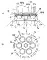
また、従来から、図7に示すように、外形が砲弾型に形成され且つ高出力のLEDチップを用いた複数の発光部2”と、人体から放射される赤外線を検知する赤外線センサ素子からなる人感センサ(以下、センサ部という)3”と、円板状に形成され且つ一表面側における中央部にセンサ部3”が配設されるとともにセンサ部3”の周辺に複数の発光部2”が配設されたベース基板1”(図7(b)参照)と、円筒状に形成され且つ内部にベース基板1”を収納する器具本体10”と、透光性材料により円板状に形成され且つベース基板1”の前記一表面側に対向する形で器具本体10”に固定されるカバー31”とを備える照明器具が提案されている。  Further, conventionally, as shown in FIG. 7, the outer shape is formed into a bullet-shaped and includes a plurality oflight emitting portions 2 ″ using high-power LED chips, and an infrared sensor element for detecting infrared rays emitted from the human body. A human sensor (hereinafter referred to as a sensor unit) 3 ″ and asensor unit 3 ″ which is formed in a disc shape and is disposed at the center on one surface side, and a plurality oflight emitting units 2 around thesensor unit 3 ″. Abase substrate 1 "" (see FIG. 7 (b)), aninstrument body 10 "formed in a cylindrical shape and containing thebase substrate 1", and a disc-like material made of a translucent material. There has been proposed a lighting fixture including acover 31 ″ that is formed and fixed to thefixture body 10 ″ so as to face the one surface side of thebase substrate 1 ″.

図7(a),(b)に示す構成の照明器具では、発光部2”から放射される光(図7(a)の一点鎖線参照)がセンサ部3”の一部に遮られないように、センサ部3”と発光部2”とを離間して配置している。つまり、図7(b)に示すように、センサ部3”の周辺は、発光部2”を配置することが制限された発光部配置禁止領域(図7(b)における一点鎖線で囲まれた領域)としている。  In the lighting apparatus having the configuration shown in FIGS. 7A and 7B, the light emitted from thelight emitting unit 2 ″ (see the one-dot chain line in FIG. 7A) is not blocked by a part of thesensor unit 3 ″. In addition, thesensor unit 3 ″ and thelight emitting unit 2 ″ are arranged apart from each other. That is, as shown in FIG. 7B, the periphery of thesensor unit 3 ″ is surrounded by a light-emitting unit arrangement prohibition region (FIG. 7B) in which the light-emittingunit 2 ″ is restricted. Area).

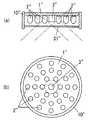
また、従来から、図8に示すように、LEDチップと当該LEDチップから放射された光によって励起され前記LEDチップとは異なる色の光を放射する蛍光体を分散させた透光性材料によりドーム状に形成された色変換部材とを有する複数の発光部102”と、矩形板状に形成され且つ一面側に発光部102”が取着されるとともにベース基板1”に形成された配線パターン(図示せず)に電気的に接続する接続端子101b”が設けられた発光部取付基板101”と、図7に示す構成と同様の赤外線センサ素子(以下、センサ部という)3”と、円板状に形成され且つ一表面側における中央部にセンサ部3”が配設されるとともにセンサ部3”の周辺に複数の貫通孔1a”が貫設されたベース基板1”(図8(a)参照)と、有底円筒状に形成されベース基板1”を収納する器具本体110”と、透光性材料により円板状に形成され且つベース基板1”の前記一表面側に対向する形で器具本体110”に固定されるカバー31”とを備え、発光部取付基板101”が、貫通孔1a”に発光部102”を挿入する形でベース基板1”の前記他表面側に取り付けられた照明器具が提案されている。ここに、ベース基板1”の前記他表面側には、放熱用部材54”が配設されており、発光部取付基板101”が放熱用部材54”に接触している。しかして、発光部102”で発生した熱は、放熱用部材54”および器具本体110”を介して外部に放熱される。  Conventionally, as shown in FIG. 8, the dome is made of a light-transmitting material in which an LED chip and a phosphor that is excited by light emitted from the LED chip and emits light of a color different from the LED chip are dispersed. A plurality oflight emitting portions 102 ″ having a color conversion member formed in a shape, and a wiring pattern (formed on thebase substrate 1 ″ while thelight emitting portion 102 ″ is attached to one surface side and is formed in a rectangular plate shape. A light emittingpart mounting substrate 101 "provided with aconnection terminal 101b" for electrical connection to an unillustrated), an infrared sensor element (hereinafter referred to as a sensor part) 3 "having the same structure as shown in FIG. Abase substrate 1 ″ (see FIG. 8A) having asensor portion 3 ″ disposed in the center on one surface side and a plurality of throughholes 1a ″ extending around thesensor portion 3 ″. See) and cylindrical shape with bottom An instrumentmain body 110 ″ that is formed and accommodates thebase substrate 1 ″, and a cover that is formed in a disc shape with a light-transmitting material and is fixed to the instrumentmain body 110 ″ so as to face the one surface side of thebase substrate 1 ″ 31 ”, and the lightfixture mounting substrate 101 ″ is mounted on the other surface side of thebase substrate 1 ″ by inserting thelight emitting portion 102 ″ into the throughhole 1a ″. Further, aheat radiating member 54 ″ is disposed on the other surface side of thebase substrate 1 ″, and the light emittingportion mounting substrate 101 ″ is in contact with theheat radiating member 54 ″. The heat generated in “is radiated to the outside through theheat radiating member 54 ″ and the instrumentmain body 110 ″.

図8(a)(b)に示す構成の照明器具では、発光部102”から放射される光(図8(a)の一点鎖線参照)がセンサ部3”の一部に遮られないように、センサ部3”と発光部102”とを離間して配置している。つまり、図8(b)に示すように、センサ部3”の周辺は、発光部102”の配置が制限された発光部配置禁止領域(図8(b)における一点鎖線で囲まれた領域)としている。  In the lighting fixture having the configuration shown in FIGS. 8A and 8B, the light emitted from thelight emitting unit 102 ″ (see the one-dot chain line in FIG. 8A) is not blocked by a part of thesensor unit 3 ″. Thesensor unit 3 ″ and thelight emitting unit 102 ″ are arranged apart from each other. That is, as shown in FIG. 8B, the periphery of thesensor unit 3 ″ is a light-emitting unit arrangement prohibited region in which the arrangement of the light-emitting unit 102 ″ is restricted (a region surrounded by a one-dot chain line in FIG. 8B). It is said.

特開2001−325810号公報JP 2001-325810 A

しかしながら、図6に示す構成の照明器具では、センサ部3’の温度上昇を抑制するとともに発光部2’から放射される光の一部がセンサ部3’により遮られないようにするために、ベース基板1’の中央部に前記発光部配置禁止領域を設ける必要があり、照明器具の配光分布が、中央部が暗く周辺部が明るい配光分布(いわゆるドーナツ状の配光分布)となるおそれがあった。  However, in the lighting fixture having the configuration shown in FIG. 6, in order to suppress the temperature rise of thesensor unit 3 ′ and prevent a part of the light emitted from thelight emitting unit 2 ′ from being blocked by thesensor unit 3 ′, It is necessary to provide the light emitting part disposition prohibition region at the center part of thebase substrate 1 ′, and the light distribution of the luminaire is a light distribution that is dark in the center and bright in the peripheral part (so-called donut-shaped light distribution). There was a fear.

また、図7に示す構成の照明器具においても、発光部2”から放射される光の一部がセンサ部3”により遮られないようにするために、センサ部3”の周辺に発光部2”を配置することが制限された領域である発光部配置禁止領域を形成する必要があり、均一な配光分布が得られないおそれがあった。更に、図8に示す構成の照明器具においても、図7に示す構成の照明器具と同様に、センサ部3”の周辺に発光部102”を配置することが制限された領域である発光部配置禁止領域を形成する必要があり、均一な照明器具の配光分布が得られないおそれがあった。  Also in the lighting fixture having the configuration shown in FIG. 7, in order to prevent a part of the light emitted from thelight emitting section 2 ″ from being blocked by thesensor section 3 ″, thelight emitting section 2 is provided around thesensor section 3 ″. Therefore, it is necessary to form a light emitting portion disposition prohibiting region, which is a region where the arrangement of “is restricted”, and there is a possibility that a uniform light distribution cannot be obtained. Further, in the lighting fixture having the configuration shown in FIG. 8, similarly to the lighting fixture having the configuration shown in FIG. 7, the arrangement of the light emitting portion, which is a region where thelight emitting portion 102 ″ is limited to be arranged around thesensor portion 3 ″. It is necessary to form a forbidden area, and there is a possibility that a uniform light distribution of the lighting fixture cannot be obtained.

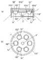
一方、照明器具の配光をより均一にするために、図9および図10に示すように、ベース基板1’の中央部に配設されたセンサ部3’に近接して発光部2’を配置すると、センサ部3’が熱源である発光部2’に近づくことになり、発光部2’で発生しベース基板1’を介してセンサ部3’に伝達する熱により、センサ部3’の温度が上昇するおそれがあった。また、図7や図8に示す構成の照明器具において、発光部2”,102”をセンサ部3”に近接して配置すると、図9や図10に示すように、発光部2”,102”から放射される光(図9(a)および図10(a)の一点鎖線参照)の一部をセンサ部3’が遮ることにより、発光部2”からの配光が制限され、照明器具の光出力が低下してしまうおそれがあった。つまり、発光部2”,102”の光軸と発光部2”,102”から放射される光の放射光量が放射光量の最大値の半分となる光の放射方向に延長された直線とのなす角度を半値角と定義したときに、発光部2”,102”から放射される光のうち、発光部2”,102”から光軸とのなす角度が半値角以下の角度となる方向に放射される光の光量が低下してしまうおそれがあった。  On the other hand, in order to make the light distribution of the luminaire more uniform, as shown in FIGS. 9 and 10, thelight emitting unit 2 ′ is placed in proximity to thesensor unit 3 ′ disposed in the center of thebase substrate 1 ′. When arranged, thesensor unit 3 ′ approaches thelight emitting unit 2 ′ that is a heat source, and the heat generated by thelight emitting unit 2 ′ and transmitted to thesensor unit 3 ′ via thebase substrate 1 ′ causes thesensor unit 3 ′. There was a risk of temperature rise. Further, in the lighting apparatus having the configuration shown in FIGS. 7 and 8, when thelight emitting portions 2 ″ and 102 ″ are arranged close to thesensor portion 3 ″, as shown in FIGS. 9 and 10, thelight emitting portions 2 ″ and 102 are arranged. The light distribution from thelight emitting unit 2 ″ is restricted by thesensor unit 3 ′ blocking a part of the light emitted from the light source (see the one-dot chain line in FIG. 9A and FIG. 10A). There was a risk that the light output of the light would decrease. That is, the optical axis of thelight emitting units 2 ″ and 102 ″ and the straight line extended in the light emitting direction in which the amount of light emitted from thelight emitting units 2 ″ and 102 ″ is half the maximum value of the amount of emitted light. When the angle is defined as a half-value angle, out of the light emitted from thelight emitting units 2 ″ and 102 ″, the light emitted from thelight emitting units 2 ″ and 102 ″ to the optical axis is an angle that is equal to or less than the half-value angle. There was a risk that the amount of light emitted would be reduced.

本願発明は、上記事由に鑑みてなされたものであり、その目的は、所定の機能を有する機能素子部の温度上昇を抑制しつつ、均一な配光分布を得ることができるとともに光出力の低下を抑制することができる照明器具を提供することにある。  The present invention has been made in view of the above-mentioned reasons, and the purpose thereof is to suppress the temperature rise of the functional element unit having a predetermined function and obtain a uniform light distribution and to reduce the light output. It is providing the lighting fixture which can suppress this.

請求項1の発明は、LEDチップを用いた複数の発光部と、所定の機能を有する機能素子部の出力に基づいて発光部への供給電力を制御することにより発光部を点灯および消灯させる制御手段を有する点灯装置とを備えた照明器具であって、板状に形成され且つ機能素子部が挿通可能な大きさの機能素子部挿通孔が貫設されたベース基板と、機能素子部が取着されるとともに機能素子部を前記機能素子部挿通孔に挿通し機能素子部の一部がベース基板の一表面側に突出する形でベース基板の他表面側に配置される機能素子部取付基板と、ベース基板を保持する器具本体とを備え、機能素子部におけるベース基板の一表面側に突出した部分の周辺に前記複数の発光部が配置されるとともに、機能素子部取付基板が、機能素子部におけるベース基板の一表面側に突出した部分が各発光部の光を遮らないように配置されていることを特徴とする。  The invention according toclaim 1 is a control for turning on and off the light emitting unit by controlling the power supplied to the light emitting unit based on the outputs of the plurality of light emitting units using LED chips and the functional element unit having a predetermined function. A lighting device including a lighting device having a means, a base substrate formed in a plate shape and having a functional element portion insertion hole penetrating the functional element portion, and the functional element portion A functional element mounting substrate that is placed on the other surface side of the base substrate in such a manner that the functional element portion is inserted through the functional element portion insertion hole and a part of the functional element portion protrudes to the one surface side of the base substrate. And a fixture main body for holding the base substrate, wherein the plurality of light emitting portions are arranged around a portion of the functional element portion that protrudes to one surface side of the base substrate, and the functional element portion mounting substrate is a functional element. Base group Wherein the one surface side protruding portion of the are arranged so as not to block the light of each light-emitting portion.

この発明によれば、板状に形成され且つ機能素子部が挿通可能な大きさの機能素子部挿通孔が貫設されたベース基板と、機能素子部が取着されるとともに機能素子部を前記機能素子部挿通孔に挿通し機能素子部の一部がベース基板の一表面側に突出する形でベース基板の他表面側に配置される機能素子部取付基板とを備え、機能素子部におけるベース基板の一表面側に突出した部分の周辺に前記複数の発光部が配置されるとともに、機能素子部取付基板が、機能素子部におけるベース基板の前記一表面側に突出した部分が各発光部の光を遮らないように配置されていることにより、発光部の配光が機能素子部により制限されるのを抑制することができるので、均一な照明器具の配光分布を得ることができるとともに照明器具の光出力の低下を抑制することができる。また、機能素子部が、ベース基板とは別の機能素子部取付基板に取着されていることにより、発光部と機能素子部とが同一のベース基板に取着されている場合に比べて、発光部で発生しベース基板を介して機能素子部に伝達する熱を低減させることができるので、機能素子部の温度上昇を抑制することができる。  According to the present invention, a base substrate that is formed in a plate shape and through which a functional element portion insertion hole having a size through which the functional element portion can be inserted, the functional element portion is attached, and the functional element portion is A functional element mounting board disposed on the other surface side of the base substrate in such a manner that a part of the functional element portion is inserted through the functional element portion insertion hole and protrudes on one surface side of the base substrate. The plurality of light emitting portions are arranged around a portion protruding to one surface side of the substrate, and the functional element mounting substrate is a portion of the functional element portion protruding to the one surface side of the base substrate. By arranging so as not to block light, it is possible to suppress the light distribution of the light emitting unit from being restricted by the functional element unit, so that it is possible to obtain a uniform light distribution of the luminaire and illumination Reduce the light output of the instrument It is possible to win. In addition, since the functional element unit is attached to the functional element unit mounting substrate different from the base substrate, compared to the case where the light emitting unit and the functional element unit are attached to the same base substrate, Since heat generated in the light emitting part and transmitted to the functional element part via the base substrate can be reduced, an increase in temperature of the functional element part can be suppressed.

請求項2の発明は、請求項1の発明において、前記発光部が取着される発光部取付基板を備え、前記ベース基板には、前記機能素子部挿通孔の周辺に発光部取付基板に取着された前記発光部を各別に挿通可能な大きさの複数の発光部挿通孔が貫設され、発光部取付基板が、前記発光部を前記発光部挿通孔に挿通するとともに前記機能素子部取付基板に重ならない形で前記ベース基板の前記他表面側に配置されてなることを特徴とする。  According to a second aspect of the present invention, in the first aspect of the invention, the light emitting unit mounting substrate to which the light emitting unit is attached is provided, and the base substrate is attached to the light emitting unit mounting substrate around the functional element unit insertion hole. A plurality of light emitting portion insertion holes of a size that can be inserted through the light emitting portions that are attached to each other are penetrated, and a light emitting portion mounting substrate passes the light emitting portion through the light emitting portion insertion hole and is attached to the functional element portion It is arranged on the other surface side of the base substrate so as not to overlap the substrate.

この発明によれば、前記発光部が取着される発光部取付基板を備え、前記ベース基板には、前記機能素子部挿通孔の周辺に発光部取付基板に取着された前記発光部を各別に挿通可能な大きさの複数の発光部挿通孔が貫設され、発光部取付基板が、前記発光部を前記発光部挿通孔に挿通するとともに前記機能素子部取付基板に重ならない形で前記ベース基板の前記他表面側に配置されてなることにより、前記発光部が前記ベース基板に取着されている場合に比べて、前記発光部で発生し前記ベース基板を介して前記機能素子部に伝達する熱を低減することができるので、前記機能素子部の温度上昇を抑制することができる。  According to this invention, the light emitting unit mounting substrate to which the light emitting unit is attached is provided, and the light emitting unit attached to the light emitting unit mounting substrate is disposed around the functional element unit insertion hole on the base substrate. A plurality of light emitting portion insertion holes of a size that can be separately inserted are provided, and the light emitting portion mounting substrate passes through the light emitting portion through the light emitting portion insertion hole and does not overlap the functional element portion mounting substrate. By being arranged on the other surface side of the substrate, the light emitting portion is generated in the light emitting portion and transmitted to the functional element portion via the base substrate as compared with the case where the light emitting portion is attached to the base substrate. Since the heat to perform can be reduced, the temperature rise of the said functional element part can be suppressed.

請求項3の発明は、請求項2の発明において、前記発光部および前記機能素子部で発生した熱を前記器具本体を介して外部に放熱するための放熱用部材を備え、前記機能素子部取付基板の厚みが、前記発光部取付基板の厚みと同じになるように設定され、放熱用部材が、前記器具本体、前記機能素子部取付基板および前記発光部取付基板に接触する形で配置されてなることを特徴とする。  The invention according toclaim 3 is the invention according toclaim 2, further comprising a heat radiating member for radiating heat generated in the light emitting part and the functional element part to the outside through the instrument body, and the functional element part mounting The thickness of the substrate is set to be the same as the thickness of the light emitting unit mounting substrate, and the heat dissipating member is arranged in contact with the instrument body, the functional element unit mounting substrate, and the light emitting unit mounting substrate. It is characterized by becoming.

この発明によれば、前記発光部および前記機能素子部で発生した熱を前記器具本体を介して外部に放熱するための放熱用部材を備え、前記機能素子部取付基板の厚みが、前記発光部取付基板の厚みと同じになるように設定され、放熱用部材が、前記器具本体、前記機能素子部取付基板および前記発光部取付基板に接触する形で配置されてなることにより、前記機能素子部の温度が放熱用部材の温度に比べて高い場合において、前記機能素子部で発生した熱を外部に効率よく放熱することができるので、前記機能素子部の温度上昇を抑制することができる。  According to this invention, it is provided with the heat radiating member for radiating the heat generated in the light emitting part and the functional element part to the outside via the instrument body, and the thickness of the functional element part mounting substrate is the light emitting part. It is set to be the same as the thickness of the mounting substrate, and the heat radiating member is arranged in contact with the instrument main body, the functional element mounting substrate, and the light emitting unit mounting substrate, whereby the functional element unit When the temperature is higher than the temperature of the heat radiating member, the heat generated in the functional element portion can be efficiently radiated to the outside, so that the temperature rise of the functional element portion can be suppressed.

請求項4の発明は、請求項2の発明において、前記発光部および前記機能素子部で発生した熱を前記器具本体を介して外部に放熱するための放熱用部材を備え、前記機能素子部取付基板の厚みが、前記発光部取付基板の厚みよりも薄くなるように設定され、放熱用部材が、前記器具本体および前記発光部取付基板に接触し且つ前記機能素子部取付基板に接触しない形で配置されてなることを特徴とする。  The invention ofclaim 4 is the invention ofclaim 2, further comprising a heat radiating member for radiating heat generated in the light emitting part and the functional element part to the outside via the instrument body, and the functional element part mounting The thickness of the substrate is set to be thinner than the thickness of the light emitting unit mounting substrate, and the heat dissipating member is in contact with the fixture body and the light emitting unit mounting substrate and not in contact with the functional element unit mounting substrate. It is characterized by being arranged.

この発明によれば、前記発光部および前記機能素子部で発生した熱を前記器具本体を介して外部に放熱するための放熱用部材を備え、前記機能素子部取付基板の厚みが、前記発光部取付基板の厚みよりも薄くなるように設定され、放熱用部材が、前記器具本体および前記発光部取付基板に接触し且つ前記機能素子部取付基板に接触しない形で配置されてなることにより、前記機能素子部の温度が放熱用部材の温度に比べて低い場合において、前記発光部で発生し放熱用部材に伝達した熱が前記機能素子部に伝わるのを抑制することができるので、前記機能素子部の温度上昇を抑制することができる。  According to this invention, it is provided with the heat radiating member for radiating the heat generated in the light emitting part and the functional element part to the outside via the instrument body, and the thickness of the functional element part mounting substrate is the light emitting part. It is set so as to be thinner than the thickness of the mounting substrate, and the heat dissipating member is arranged in contact with the instrument body and the light emitting unit mounting substrate and not in contact with the functional element unit mounting substrate, When the temperature of the functional element portion is lower than the temperature of the heat radiating member, the heat generated in the light emitting portion and transmitted to the heat radiating member can be suppressed from being transmitted to the functional element portion. The temperature rise of the part can be suppressed.

請求項1の発明によれば、機能素子部におけるベース基板の一表面側に突出した部分の周辺に複数の発光部が配置されるとともに、機能素子部取付基板が、機能素子部におけるベース基板の前記一表面側に突出した部分が発光部からの光を遮らないように配置されていることにより、発光部の配光が制限されるのを抑制することができるので、均一な配光を得ることができるとともに光出力の低下を抑制することができる。また、機能素子部が、ベース基板とは別の機能素子部取付基板に取着されていることにより、発光部と機能素子部とが同一のベース基板に取着されている場合に比べて、発光部で発生しベース基板を介して機能素子部に伝達する熱を低減させることができるので、機能素子部の温度上昇を抑制することができる。  According to the first aspect of the present invention, the plurality of light emitting portions are disposed around the portion of the functional element portion that protrudes toward the one surface side of the base substrate, and the functional element portion mounting substrate is provided on the base substrate of the functional element portion. Since the portion protruding to the one surface side is arranged so as not to block the light from the light emitting portion, it is possible to suppress the light distribution of the light emitting portion from being restricted, so that a uniform light distribution is obtained. And a decrease in light output can be suppressed. In addition, since the functional element unit is attached to the functional element unit mounting substrate different from the base substrate, compared to the case where the light emitting unit and the functional element unit are attached to the same base substrate, Since heat generated in the light emitting part and transmitted to the functional element part via the base substrate can be reduced, an increase in temperature of the functional element part can be suppressed.

実施形態1の照明器具を示し、(a)は概略断面図、(b)は概略平面図である。The lighting fixture ofEmbodiment 1 is shown, (a) is a schematic sectional drawing, (b) is a schematic plan view.同上の照明装置の概略斜視図である。It is a schematic perspective view of an illuminating device same as the above.同上の照明装置の回路ブロック図である。It is a circuit block diagram of an illuminating device same as the above.実施形態2の照明器具を示し、(a)は概略断面図、(b)は概略平面図である。The lighting fixture ofEmbodiment 2 is shown, (a) is a schematic sectional drawing, (b) is a schematic plan view.実施形態3の照明器具を示し、(a)は概略断面図、(b)は概略平面図である。The lighting fixture ofEmbodiment 3 is shown, (a) is a schematic sectional drawing, (b) is a schematic plan view.従来例の照明器具における一部破断した側面図である。It is the partially broken side view in the lighting fixture of a prior art example.他の従来例の照明器具を示し、(a)は概略断面図、(b)は概略平面図である。The lighting fixture of another prior art example is shown, (a) is a schematic sectional drawing, (b) is a schematic plan view.他の従来例の照明器具を示し、(a)は概略断面図、(b)は概略平面図である。The lighting fixture of another prior art example is shown, (a) is a schematic sectional drawing, (b) is a schematic plan view.他の従来例の照明器具の概略断面図である。It is a schematic sectional drawing of the lighting fixture of another conventional example.他の従来例の照明器具の概略断面図である。It is a schematic sectional drawing of the lighting fixture of another conventional example.

(実施形態1)
以下、本実施形態の照明器具について図1乃至図3に基づいて説明する。
(Embodiment 1)
Hereinafter, the lighting fixture of this embodiment is demonstrated based on FIG. 1 thru | or FIG.

本実施形態の照明器具は、天井埋め込み型LED照明器具であって、LEDチップ(図示せず)を用いた複数の発光部2と、所定の機能として人体から放射される赤外線を検知する機能を有する赤外線センサ素子を用いた機能素子部であるセンサ部3と、センサ部3の出力に基づいて発光部2への供給電力を制御することにより発光部2を点灯および消灯させる制御手段である制御回路部43(図3参照)を有する点灯装置4(図3参照)と、円板状に形成され且つセンサ部3が挿通可能な大きさの平面視円形状の開口形状を有するセンサ部挿通孔(機能素子部挿通孔)1bが貫設され一表面側に発光部2が配設された第1のプリント基板からなるベース基板1と、一面側にセンサ部3が配設されるとともにセンサ部3をセンサ部挿通孔1bに挿通した形でベース基板1の他表面側に取着される第2のプリント基板からなる機能素子部取付基板であるセンサ部取付基板201と、ベース基板1を保持する器具本体10とを備える。ここに、センサ部3の一部は、センサ部挿通孔1bからベース基板1の前記一表面側に突出している。  The lighting fixture of this embodiment is a ceiling-embedded LED lighting fixture, and has a plurality of light emittingunits 2 using LED chips (not shown) and a function of detecting infrared rays emitted from a human body as a predetermined function. Asensor unit 3 that is a functional element unit using an infrared sensor element and a control unit that controls the power supplied to thelight emitting unit 2 based on the output of thesensor unit 3 to turn on and off thelight emitting unit 2 The lighting device 4 (see FIG. 3) having the circuit portion 43 (see FIG. 3) and the sensor portion insertion hole formed in a disk shape and having a circular opening in a plan view so that thesensor portion 3 can be inserted. (Functional element portion insertion hole) Abase substrate 1 made of a first printed circuit board having a light-transmittingportion 2 disposed on one surface side and asensor portion 3 disposed on one surface side and a sensor portion. 3 is the sensorpart insertion hole 1b. Comprising a sensorunit mounting substrate 201 is a functional element mounting substrate formed of a second printed circuit board is attached to the other surface side of thebase substrate 1 in the insertion form, and a fixturemain body 10 for holding thebase substrate 1. Here, a part of thesensor part 3 protrudes from the sensorpart insertion hole 1 b to the one surface side of thebase substrate 1.

センサ部3は、ベース基板1の中央部に貫設された上述のセンサ部挿通孔1bに挿通されている。また、複数の発光部2は、センサ部3におけるベース基板1の前記一表面側に突出した部分を囲む1つの円周方向において等間隔で配設されている。なお、センサ部3は、赤外線センサ素子として、焦電型センサ素子(図示せず)を用いている。  Thesensor unit 3 is inserted through the above-described sensorunit insertion hole 1 b penetrating through the central portion of thebase substrate 1. The plurality of light emittingunits 2 are arranged at equal intervals in one circumferential direction surrounding a portion of thesensor unit 3 that protrudes toward the one surface side of thebase substrate 1. Thesensor unit 3 uses a pyroelectric sensor element (not shown) as an infrared sensor element.

発光部2は、外形が砲弾型の発光装置であって、LEDチップと、前記LEDチップの正電極および負電極それぞれに電気的に接続された一対のリード(図示せず)と、前記LEDチップから放射された光によって励起され前記LEDチップとは異なる色の光を放射する蛍光体を分散させた透光性樹脂材料からなる透光性部材(図示せず)と、透光性のエポキシ樹脂等からなり前記一対のリードを砲弾型にモールドしてなる光学部材2aとを備えている。ここに、前記一対のリードの一方には、カップ(図示せず)が連続一体に形成されており、当該カップの内底面に前記LEDチップが実装されている。また、前記透光性部材は、前記LEDチップが実装された前記カップ内に充填されている。また、前記LEDチップとして、青色光を放射するGaN系青色LEDチップが用いられ、前記透光性部材に分散させる蛍光体としては黄色蛍光体が用いられており、発光部2からは白色光が放射される。なお、発光部2は、これに限らず、例えば、前記LEDチップとして、紫外光を放射する紫外LEDチップが用いられ、前記透光性部材に分散させる蛍光体としては赤色蛍光体、緑色蛍光体および青色蛍光体を用いたものであってもよい。また、前記透光性部材として、蛍光体を含有しないものを用い、前記LEDチップとして、赤色LEDチップ、緑色LEDチップおよび青色LEDチップを用いたものであってもよい。また、発光部2は、ベース基板1に貫設された一対のリード挿通孔(図示せず)それぞれにベース基板1の前記一表面側から前記各リードを各別に挿通しベース基板1の他表面側でベース基板1の前記他表面側に形成された配線パターン(図示せず)に半田付けすることにより、ベース基板1の前記一表面側に配設される。  Thelight emitting unit 2 is a bullet-shaped light emitting device having an outer shape, an LED chip, a pair of leads (not shown) electrically connected to the positive electrode and the negative electrode of the LED chip, and the LED chip A translucent member (not shown) made of a translucent resin material in which a phosphor that is excited by light emitted from the LED chip and emits light of a color different from that of the LED chip is dispersed, and a translucent epoxy resin And anoptical member 2a formed by molding the pair of leads into a bullet shape. Here, a cup (not shown) is integrally formed on one of the pair of leads, and the LED chip is mounted on the inner bottom surface of the cup. The translucent member is filled in the cup on which the LED chip is mounted. In addition, a GaN blue LED chip that emits blue light is used as the LED chip, a yellow phosphor is used as the phosphor dispersed in the translucent member, and white light is emitted from thelight emitting unit 2. Radiated. Thelight emitting unit 2 is not limited to this. For example, an ultraviolet LED chip that emits ultraviolet light is used as the LED chip, and the phosphors dispersed in the translucent member are red phosphors and green phosphors. Alternatively, a blue phosphor may be used. Moreover, what does not contain fluorescent substance as the said translucent member may be used, and a red LED chip, a green LED chip, and a blue LED chip may be used as said LED chip. In addition, thelight emitting unit 2 inserts each lead separately from the one surface side of thebase substrate 1 into each of a pair of lead insertion holes (not shown) penetrating thebase substrate 1. By soldering to a wiring pattern (not shown) formed on the other surface side of thebase substrate 1 on the side, thebase substrate 1 is disposed on the one surface side.

本実施形態の照明器具は、図2に示すように、金属(例えば、Al、Cuなどの熱伝導率の高い金属)により円筒状に形成され点灯装置4(図3参照)を内部に収納する第1の筐体11と、円筒状部材により形成され且つ当該円筒状部材の下端部の外周全体から外方に延出した外鍔部12aを有する円筒状の第2の筐体12と、第1の筐体11の外側における上端側に配設され点灯装置4へ給電するための端子台15と、第2の筐体12の外側に設けられ第2の筐体12を造営材である天井材(図示せず)に取り付けるための3つの取付ばね14とを備えている。ここで、第1の筐体11と第2の筐体12と後述の隔壁11aは、連続一体に形成されており、第1の筐体11と第2の筐体12と隔壁11aとで器具本体10を構成している。前記天井材には、平面視円形状の取付孔(図示せず)が貫設されている。器具本体10が前記天井材に取り付けられた状態では、第2の筐体12の外鍔部12aが前記取付孔の周部下面に当接するとともに各取付ばね14の一部が前記取付孔の周部上面に弾接している。即ち、器具本体10は、第2の筐体12の外鍔部12aと各取付ばね14とにより前記天井材を挟持する形で、前記天井材に固定される。  As shown in FIG. 2, the lighting fixture of the present embodiment is formed in a cylindrical shape from a metal (for example, a metal having high thermal conductivity such as Al or Cu), and houses the lighting device 4 (see FIG. 3). Afirst casing 11, a cylindricalsecond casing 12 formed of a cylindrical member and having anouter flange portion 12 a extending outward from the entire outer periphery of the lower end portion of the cylindrical member; Aterminal block 15 provided on the upper end side of the outer side of onecasing 11 for supplying power to thelighting device 4, and a ceiling provided on the outer side of thesecond casing 12 and thesecond casing 12 being a construction material. And three attachment springs 14 for attachment to a material (not shown). Here, thefirst casing 11, thesecond casing 12, and apartition wall 11 a to be described later are formed continuously and integrally. Amain body 10 is configured. A mounting hole (not shown) having a circular shape in plan view is provided through the ceiling material. In a state where theinstrument body 10 is attached to the ceiling material, theouter flange portion 12a of thesecond housing 12 abuts on the lower surface of the peripheral portion of the attachment hole, and a part of eachattachment spring 14 surrounds the attachment hole. It is in elastic contact with the top surface of the club. That is, the instrumentmain body 10 is fixed to the ceiling material in such a manner that the ceiling material is sandwiched between theouter flange portion 12a of thesecond housing 12 and the mounting springs 14.

第1の筐体11と第2の筐体12とは、器具本体10と連続一体に形成された隔壁11aで仕切られており、隔壁11aには、ベース基板1が取付ねじ等により取着されている。隔壁11aには、点灯装置4からベース基板1に取着された発光部2に通電するための電線(図示せず)を挿通させるための電線挿通孔(図示せず)と、センサ部3と制御回路部43(図3参照)とを電気的に接続する信号線(図示せず)を挿通させるための信号線挿通孔(図示せず)が設けられている。また、図1に示すように、センサ部3で発生した熱を器具本体10を介して外部に放熱するための放熱用部材54が、器具本体10の一部を構成する第1の筐体11と第2の筐体12との間の隔壁11aに接触する形で配置されている。ここに、放熱用部材54としては、例えば、エポキシ樹脂中に無機フィラーを高密度充填してなるシート状の封止材を使用することができる。また、器具本体10の第2の筐体12における隔壁11a側とは反対側には、透光性材料により円板状に形成された透光パネル31が取り付けられている。  Thefirst housing 11 and thesecond housing 12 are partitioned by apartition wall 11a formed continuously and integrally with theinstrument body 10, and thebase substrate 1 is attached to thepartition wall 11a by a mounting screw or the like. ing. In thepartition wall 11a, an electric wire insertion hole (not shown) for inserting an electric wire (not shown) for energizing thelight emitting portion 2 attached to thebase substrate 1 from thelighting device 4, asensor portion 3, A signal line insertion hole (not shown) for inserting a signal line (not shown) that electrically connects the control circuit unit 43 (see FIG. 3) is provided. Further, as shown in FIG. 1, aheat radiating member 54 for radiating heat generated in thesensor unit 3 to the outside through the instrumentmain body 10 includes afirst housing 11 constituting a part of the instrumentmain body 10. And in contact with thepartition wall 11a between thefirst housing 12 and thesecond housing 12. Here, as theheat radiating member 54, for example, a sheet-like sealing material formed by high density filling of an inorganic filler in an epoxy resin can be used. Moreover, thetranslucent panel 31 formed in the disk shape with the translucent material is attached to the opposite side to thepartition 11a side in the 2nd housing | casing 12 of the instrumentmain body 10. FIG.

ここで、透光パネル31は、外周部の複数箇所に遠心方向に突出する突出部(図示せず)が設けられており、当該複数の突出部が円筒状の第2の筐体12における隔壁11a側とは反対側における周方向に沿って形成された溝部(図示せず)に嵌合した形で取り付けられる。また、当該溝部は、周方向における複数箇所に切欠部(図示せず)が形成されており、透光パネル31は、前記突出部を前記溝部の複数箇所に形成された前記切欠部から挿入した後に周方向に回転させることで前記突出部が前記溝部に嵌合する。  Here, thetranslucent panel 31 is provided with protrusions (not shown) protruding in the centrifugal direction at a plurality of locations on the outer peripheral portion, and the plurality of protrusions are partition walls in the cylindricalsecond housing 12. It is attached in a form fitted into a groove (not shown) formed along the circumferential direction on the side opposite to the 11a side. Moreover, the said groove part has the notch part (not shown) formed in the multiple places in the circumferential direction, and thetranslucent panel 31 inserted the said protrusion part from the said notch part formed in the several places of the said groove part. The protrusion is fitted into the groove by rotating in the circumferential direction later.

点灯装置4は、図3に示すように、商用電源ACから供給される交流電力を整流した後に平滑化して直流電流を出力する整流平滑部41と、複数の発光部2に一定の大きさの電流を供給するための定電流電源部42と、センサ部3に電気的に接続されセンサ部3からの出力に基づいて定電流電源部42から前記複数の発光部2へ供給される電力を制御する前記制御手段である制御回路部43と、制御回路部43に電力を供給するための制御電源部44とを備える。  As shown in FIG. 3, thelighting device 4 includes a rectifying / smoothingunit 41 that rectifies AC power supplied from the commercial power supply AC and then smoothes and outputs a DC current, and a plurality of light emittingunits 2 having a certain size. A constant currentpower supply unit 42 for supplying current and electric power that is electrically connected to thesensor unit 3 and is supplied from the constant currentpower supply unit 42 to the plurality of light emittingunits 2 based on an output from the sensor unit 3 Acontrol circuit unit 43 serving as the control means, and a controlpower supply unit 44 for supplying power to thecontrol circuit unit 43.

制御回路部43には、センサ部3からの出力に基づいて後述の定電流電源部42に対して発光部2を消灯させる消灯制御指示または発光部2を点灯させる点灯制御指示を行う点灯消灯指示手段(図示せず)を備えている。ここに、前記点灯消灯指示手段は、適宜の制御プログラムを搭載したマイクロコンピュータ(図示せず)により実現されている。  Based on the output from thesensor unit 3, thecontrol circuit unit 43 performs a turn-off control instruction to turn off the light-emittingunit 2 or a turn-on instruction to turn on the light-emittingunit 2 with respect to the constant currentpower supply unit 42 described later. Means (not shown) are provided. Here, the on / off instruction means is realized by a microcomputer (not shown) equipped with an appropriate control program.

制御電源部44は、例えば、整流平滑部41の出力端間に接続された第1のスイッチング素子(図示せず)と第1のダイオード(図示せず)とからなる直列回路と、前記第1のダイオードの両端間に接続されたインダクタ(図示せず)と平滑用コンデンサ(図示せず)とからなる直列回路と、前記第1のスイッチング素子に接続され前記第1のスイッチング素子のオン・オフ時間を制御するスイッチング電源用IC(図示せず)とからなる降圧チョッパ回路で構成されている。制御電源部44の一部を構成する前記平滑コンデンサの両端間には、制御回路部43が接続されており、制御電源部44から制御回路部43に直流電圧が出力される。  The controlpower supply unit 44 includes, for example, a series circuit including a first switching element (not shown) and a first diode (not shown) connected between output terminals of the rectifying and smoothingunit 41, and the first A series circuit composed of an inductor (not shown) and a smoothing capacitor (not shown) connected between both ends of the diode, and on / off of the first switching element connected to the first switching element. It comprises a step-down chopper circuit comprising a switching power supply IC (not shown) for controlling time. Acontrol circuit unit 43 is connected between both ends of the smoothing capacitor constituting a part of the controlpower supply unit 44, and a DC voltage is output from the controlpower supply unit 44 to thecontrol circuit unit 43.

定電流電源部42は、例えば、整流平滑部41の出力端間に接続された第2のスイッチング素子(図示せず)と第2のダイオード(図示せず)とからなる直列回路と、前記第2のダイオードの両端間に接続されたチョークコイルからなるインダクタ(図示せず)と平滑用コンデンサ(図示せず)とからなる直列回路と、前記第2のスイッチング素子に接続され前記第2のスイッチング素子のオン・オフ時間を制御するコントローラとからなる降圧チョッパ回路で構成されている。ここに、前記コントローラは、前記マイクロコンピュータに適宜の制御プログラムを搭載することにより実現されている。また、定電流電源部42の一部を構成する前記平滑コンデンサの両端間には、複数の発光部2の直列回路が接続されており、定電流電源部42から複数の発光部2の直列回路に一定の直流電流を出力する。ここで、前記コントローラは、前記点灯消灯指示手段からの前記点灯制御指示に基づいて、定電流電源部42から複数の発光部2への通電を開始するように定電流電源部42を制御して、複数の発光部2を点灯させる。一方、前記コントローラは、前記点灯消灯制御手段からの前記消灯制御指示に基づいて、定電流電源部42から発光部2への電流供給を遮断するように定電流電源部42を制御して複数の発光部2を消灯させる。  The constant currentpower supply unit 42 includes, for example, a series circuit including a second switching element (not shown) and a second diode (not shown) connected between output terminals of the rectifying and smoothingunit 41, and the first A series circuit comprising an inductor (not shown) made of a choke coil connected between both ends of the two diodes and a smoothing capacitor (not shown), and the second switching element connected to the second switching element. It comprises a step-down chopper circuit comprising a controller that controls the on / off time of the element. Here, the controller is realized by mounting an appropriate control program on the microcomputer. Further, a series circuit of a plurality of light emittingunits 2 is connected between both ends of the smoothing capacitor constituting a part of the constant currentpower source unit 42, and the series circuit of the plurality of light emittingunits 2 from the constant currentpower source unit 42. Output a constant DC current. Here, the controller controls the constant currentpower supply unit 42 so as to start energization from the constant currentpower supply unit 42 to the plurality of light emittingunits 2 based on the lighting control instruction from the lighting on / off instruction unit. The plurality of light emittingunits 2 are turned on. On the other hand, the controller controls the constant currentpower supply unit 42 so as to cut off the current supply from the constant currentpower supply unit 42 to thelight emitting unit 2 based on the turn-off control instruction from the turn-on / off control means. Thelight emitting unit 2 is turned off.

整流平滑部41は、商用電源ACから供給される交流電流を全波整流するダイオードブリッジ(図示せず)と、前記ダイオードブリッジの出力端間に接続され前記ダイオードブリッジから出力される脈流を平滑化するための平滑用コンデンサ(図示せず)とから構成される。  The rectifying / smoothingunit 41 is connected between a diode bridge (not shown) for full-wave rectification of an alternating current supplied from a commercial power supply AC and an output terminal of the diode bridge, and smoothes a pulsating current output from the diode bridge. And a smoothing capacitor (not shown).

ところで、本実施形態の照明器具では、図1に示すように、センサ部3がセンサ部取付基板201に取着され、センサ部取付基板201は、ベース基板1の中央部に設けられたセンサ部挿通孔1bを通してベース基板1の前記一表面側にセンサ部3の一部が突出する形でベース基板1の他表面側に取着されている。ここに、センサ部取付基板201は、センサ部3におけるベース基板1の前記一表面側に突出した部分が各発光部2の光を遮らないように配置される。  By the way, in the lighting fixture of this embodiment, as shown in FIG. 1, thesensor unit 3 is attached to the sensorunit mounting substrate 201, and the sensorunit mounting substrate 201 is provided in the center of thebase substrate 1. A part of thesensor portion 3 protrudes from the one surface side of thebase substrate 1 through theinsertion hole 1b and is attached to the other surface side of thebase substrate 1. Here, the sensorunit mounting substrate 201 is arranged so that the portion of thesensor unit 3 protruding to the one surface side of thebase substrate 1 does not block the light of eachlight emitting unit 2.

しかして、ベース基板1の厚みに相当する量だけセンサ部3のベース基板1の前記一表面側の突出量を小さくすることができるので、複数の発光部2それぞれの配光がセンサ部3により制限されるのを抑制することができるから、照明器具の配光の均一性の向上および光出力の低下の抑制を図ることができる。つまり、図1(b)に示すように、ベース基板1の前記一表面側において発光部2を配設することが禁止される領域である発光部配置禁止領域(図1(b)の一点鎖線の内側の領域)が、従来の図7に示す構成の照明器具における前記発光部配置禁止領域(図7(b)の一点鎖線の内側の領域)に比べて小さくなるので、照明器具の配光の均一性を向上させることができる。  Accordingly, the amount of protrusion of thebase substrate 1 of thesensor unit 3 on the one surface side can be reduced by an amount corresponding to the thickness of thebase substrate 1, so that the light distribution of each of the plurality of light emittingunits 2 is caused by thesensor unit 3. Since it can suppress that it is restrict | limited, the improvement of the uniformity of the light distribution of a lighting fixture and suppression of the fall of a light output can be aimed at. That is, as shown in FIG. 1B, the light emitting unit disposition prohibiting region (the dashed line in FIG. 1B) that is a region where thelight emitting unit 2 is prohibited to be disposed on the one surface side of thebase substrate 1. Is smaller than the light emitting portion arrangement prohibited region (region inside the one-dot chain line in FIG. 7B) in the lighting fixture having the configuration shown in FIG. Can improve the uniformity.

また、本実施形態の照明器具では、センサ部3が、ベース基板1とは別のセンサ部取付基板201に取着されていることにより、発光部2とセンサ部3とが同一のベース基板1に取着されている場合に比べて、発光部2で発生しベース基板1を介してセンサ部3に伝達する熱を低減させることができるので、センサ部3の温度上昇を抑制することができる。  Moreover, in the lighting fixture of this embodiment, since thesensor part 3 is attached to the sensor part attachment board |substrate 201 different from the base board |substrate 1, thelight emission part 2 and thesensor part 3 are the same base board 1s. Since the heat generated in thelight emitting part 2 and transmitted to thesensor part 3 through thebase substrate 1 can be reduced compared to the case where thesensor part 3 is attached to thesensor part 3, the temperature rise of thesensor part 3 can be suppressed. .

更に、従来の図7に示す構成の照明器具に比べて、複数の発光部2をセンサ部3に近づけて配置することができるので、ベース基板1の面積を小さくすることができるから、照明器具の小型化を図ることができる。  Furthermore, since the plurality of light emittingunits 2 can be arranged close to thesensor unit 3 as compared with the conventional lighting fixture having the configuration shown in FIG. 7, the area of thebase substrate 1 can be reduced. Can be miniaturized.

(実施形態2)
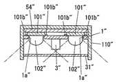
本実施形態の照明器具は、図4に示すように、矩形板状に形成され且つ一面側に発光ダイオードからなる発光部102が取着されるとともにベース基板1に形成された配線パターン(図示せず)に電気的に接続する接続端子101bが設けられたプリント基板からなる発光部取付基板101を備え、ベース基板1には、センサ部挿通孔1bの周辺に発光部取付基板101に配設された発光部102を各別に挿通可能な大きさの複数(図4では、6つ)の発光部挿通孔1aが貫設され、発光部取付基板101が、発光部102を発光部挿通孔1aに挿通するとともにプリント基板からなるセンサ部取付基板201に重ならない形でベース基板1の前記他表面側に配置されている点が実施形態1とは相違する。なお、図1に示す構成と同様の構成については同一の符号を付して説明を省略する。
(Embodiment 2)
As shown in FIG. 4, the lighting fixture of the present embodiment is formed in a rectangular plate shape, and a light-emittingportion 102 made of a light-emitting diode is attached to one side and a wiring pattern (not shown) formed on thebase substrate 1. Thebase board 1 is provided on the light emittingpart mounting board 101 around the sensorpart insertion hole 1b. The light emittingpart mounting board 101 is a printed circuit board provided withconnection terminals 101b for electrical connection. A plurality of (six in FIG. 4) light-emittingportion insertion holes 1a that can be inserted through the respective light-emittingportions 102 are provided so that the light-emittingportion mounting substrate 101 can be inserted into the light-emittingportion insertion holes 1a. It is different from the first embodiment in that it is inserted on the other surface side of thebase substrate 1 so as not to overlap the sensorportion mounting substrate 201 made of a printed circuit board. In addition, the same code | symbol is attached | subjected about the structure similar to the structure shown in FIG. 1, and description is abbreviate | omitted.

発光部取付基板101における発光部102が取着される一面側には、配線パターン(図示せず)が形成されており、接続端子101bに電気的に接続している。また、ベース基板1に形成された前記配線パターンは、点灯装置4から導出された前記電線に電気的に接続している。ここで、ベース基板1に発光部取付基板101を取り付けると同時に、発光部取付基板101に設けられた接続端子101bがベース基板1に形成された前記配線パターンに電気的に接続される。  A wiring pattern (not shown) is formed on one side of the light emittingunit mounting substrate 101 to which thelight emitting unit 102 is attached, and is electrically connected to theconnection terminal 101b. In addition, the wiring pattern formed on thebase substrate 1 is electrically connected to the electric wire led out from thelighting device 4. Here, at the same time when the light emittingunit mounting substrate 101 is attached to thebase substrate 1, theconnection terminals 101 b provided on the light emittingunit mounting substrate 101 are electrically connected to the wiring pattern formed on thebase substrate 1.

発光部102は、LEDチップ(図示せず)および当該LEDチップが実装される実装基板(図示せず)の他に、前記LEDチップから放射された光の配光を制御するドーム状に形成され前記実装基板との間にLEDチップを収納する形で前記実装基板の前記一面側に固着された透光性材料からなる光学部材(図示せず)と、前記光学部材と前記実装基板とで囲まれた空間で前記LEDチップおよび前記LEDチップに電気的に接続されたボンディングワイヤ(図示せず)を封止した透光性材料(例えば、シリコーン樹脂、エポキシ樹脂、ガラスなど)からなる封止部(図示せず)と、前記実装基板の前記一面側から前記光学部材を覆う形で配設され前記LEDチップから放射され前記封止部および前記光学部材を透過した光によって励起され前記LEDチップとは異なる色の光を放射する蛍光体を含有した透光性材料によりドーム状に形成された色変換部材(図示せず)とを備えている。また、前記色変換部材と前記光学部材の表面との間には、空気層(図示せず)が設けられている。前記空気層は、前記色変換部材内で蛍光体により前記光学部材側へ散乱される光および蛍光体から発する光が前記光学部材を透過し前記実装基板等に吸収されるのを抑制して、発光部102の光の取り出し効率を向上させる役割をする。ここに、前記LEDチップとして、青色光を放射するGaN系青色LEDチップが用いられ、前記色変換部材に含有された蛍光体としては黄色蛍光体が用いられており、発光部102からは白色光が放射される。なお、発光部102は、これに限らず、例えば、前記LEDチップとして、紫外光を放射する紫外LEDチップを用い、前記色変換部材に分散させる蛍光体として赤色蛍光体、緑色蛍光体および青色蛍光体を用いたものであってもよい。また、前記色変換部材の代わりに蛍光体を含有しない透光性部材を用い、前記LEDチップとして、赤色LEDチップ、緑色LEDチップおよび青色LEDチップを用いたものであってもよい。  In addition to the LED chip (not shown) and the mounting substrate (not shown) on which the LED chip is mounted, thelight emitting unit 102 is formed in a dome shape that controls the light distribution of the light emitted from the LED chip. An optical member (not shown) made of a translucent material fixed to the one surface side of the mounting substrate so as to house an LED chip between the mounting substrate and the optical member and the mounting substrate. A sealing portion made of a light-transmitting material (for example, silicone resin, epoxy resin, glass, etc.) that seals the LED chip and a bonding wire (not shown) electrically connected to the LED chip in the space formed (Not shown) and disposed on the mounting substrate so as to cover the optical member from the one surface side, and is excited by light emitted from the LED chip and transmitted through the sealing portion and the optical member. Wherein and a domed form color conversion member (not shown) by the light-transmitting material containing phosphors that emit light of a different color from the LED chip. An air layer (not shown) is provided between the color conversion member and the surface of the optical member. The air layer suppresses light scattered from the phosphor within the color conversion member to the optical member side and light emitted from the phosphor through the optical member and absorbed by the mounting substrate, etc. It plays a role of improving the light extraction efficiency of thelight emitting unit 102. Here, a GaN blue LED chip that emits blue light is used as the LED chip, a yellow phosphor is used as the phosphor contained in the color conversion member, and white light is emitted from thelight emitting unit 102. Is emitted. In addition, thelight emission part 102 is not restricted to this, For example, an ultraviolet LED chip | tip which radiates | emits ultraviolet light is used as said LED chip, and red fluorescent substance, green fluorescent substance, and blue fluorescent substance are used as fluorescent substance disperse | distributed to the said color conversion member. The body may be used. Further, a light transmissive member that does not contain a phosphor may be used instead of the color conversion member, and a red LED chip, a green LED chip, and a blue LED chip may be used as the LED chip.

従って、実施形態1と同様に、ベース基板1の厚みに相当する量だけセンサ部3のベース基板1の前記一表面側の突出量を小さくすることができるので、発光部102の配光がセンサ部3により制限されるのを抑制することができるから、均一な配光を得ることができるとともに光出力の低下を抑制することができる。つまり、図4(b)に示すように、ベース基板1の前記一表面側において発光部102を配置することが禁止される領域である発光部配置禁止領域(図4(b)の一点鎖線の内側の領域)が、従来の図8に示す構成の照明器具における前記発光部配置禁止領域(図8(b)の一点鎖線の内側の領域)に比べて小さくなるので、均一な配光を得ることができる。  Therefore, as in the first embodiment, the amount of protrusion on the one surface side of thebase substrate 1 of thesensor unit 3 can be reduced by an amount corresponding to the thickness of thebase substrate 1, so that the light distribution of thelight emitting unit 102 is a sensor. Since it can suppress that it is restrict | limited by thepart 3, while being able to obtain uniform light distribution, the fall of a light output can be suppressed. That is, as shown in FIG. 4B, the light emitting unit disposition prohibiting region (the dashed line in FIG. 4B) is a region where thelight emitting unit 102 is prohibited to be disposed on the one surface side of thebase substrate 1. The inner area is smaller than the light emitting portion disposition prohibiting area (the area inside the one-dot chain line in FIG. 8B) in the conventional lighting apparatus having the configuration shown in FIG. be able to.

ところで、本実施形態の照明器具では、図4に示すように、発光部102およびセンサ部3で発生した熱を器具本体10を介して外部に放熱するための放熱性樹脂シート等からなる放熱用部材54が、器具本体10の一部を構成する第1の筐体11と第2の筐体12との間の隔壁11aに接触する形で配置されている。また、図4に示すように、センサ部取付基板201の厚みが、発光部取付基板101の厚みと同じに設定され、放熱用部材54が、センサ部取付基板201および発光部取付基板101に接触している。  By the way, in the lighting fixture of this embodiment, as shown in FIG. 4, for the heat dissipation which consists of a heat-radiating resin sheet etc. for radiating the heat | fever which generate | occur | produced in thelight emission part 102 and thesensor part 3 to the exterior via the instrumentmain body 10. Themember 54 is disposed in contact with thepartition wall 11 a between thefirst housing 11 and thesecond housing 12 that constitute a part of theinstrument body 10. Further, as shown in FIG. 4, the thickness of the sensorunit mounting substrate 201 is set to be the same as the thickness of the light emittingunit mounting substrate 101, and theheat dissipation member 54 contacts the sensorunit mounting substrate 201 and the light emittingunit mounting substrate 101. is doing.

しかして、センサ部3の温度が放熱用部材54の温度に比べて高い場合において、センサ部3で発生した熱を外部に効率よく放熱することができるので、センサ部3の温度上昇を抑制することができる。  Thus, when the temperature of thesensor unit 3 is higher than the temperature of theheat radiating member 54, the heat generated in thesensor unit 3 can be efficiently radiated to the outside, so that the temperature rise of thesensor unit 3 is suppressed. be able to.

(実施形態3)
本実施形態の照明器具は、図5に示すように、センサ部取付基板201の厚みが、発光部取付基板101の厚みとに比べて薄くなるように設定され、発光部102に発生した熱を放熱するための放熱用部材54が、発光部取付基板101のみに接触する形で配置されている点が実施形態2とは相違する。なお、図4に示す構成と同様の構成については同一の符号を付して説明を省略する。
(Embodiment 3)
As shown in FIG. 5, the lighting fixture of the present embodiment is set so that the thickness of the sensorunit mounting substrate 201 is thinner than the thickness of the light emittingunit mounting substrate 101, and the heat generated in thelight emitting unit 102 is generated. The point from which theheat radiating member 54 for radiating heat | fever is arrange | positioned in the form which contacts only the light emission part attachment board |substrate 101 is different fromEmbodiment 2. FIG. In addition, about the structure similar to the structure shown in FIG. 4, the same code | symbol is attached | subjected and description is abbreviate | omitted.

しかして、センサ部3の温度が放熱用部材54の温度に比べて低い場合において、発光部2で発生し放熱用部材54に伝達した熱がセンサ部3に伝わるのを抑制することができるので、センサ部3の温度上昇を抑制することができる。  Therefore, when the temperature of thesensor unit 3 is lower than the temperature of theheat dissipation member 54, it is possible to suppress the heat generated in thelight emitting unit 2 and transmitted to theheat dissipation member 54 from being transmitted to thesensor unit 3. And the temperature rise of thesensor part 3 can be suppressed.

なお、上述の各実施形態では、センサ部3が、ベース基板1の中央部に配置される照明器具について説明したが、これに限定されるものではなく、例えば、図4に示す構成の照明器具において、発光部2が配置されている箇所にセンサ部3が配置されたものであってもよい。  In each of the above-described embodiments, the lighting unit has been described in which thesensor unit 3 is disposed at the center of thebase substrate 1. However, the present invention is not limited to this, and for example, the lighting unit having the configuration illustrated in FIG. Thesensor unit 3 may be disposed at a position where thelight emitting unit 2 is disposed.

1 ベース基板
1a 発光部挿通孔
1b センサ部挿通孔(機能素子部挿通孔)
2 発光部
3 センサ部(機能素子部)
4 点灯装置
10 器具本体
43 制御回路部(制御手段)
54 放熱用部材
101 発光部取付基板
201 センサ部取付基板(機能素子部取付基板)
1Base substrate 1a Light emittingpart insertion hole 1b Sensor part insertion hole (functional element part insertion hole)
2Light emitting part 3 Sensor part (functional element part)
4lighting device 10 appliancemain body 43 control circuit part (control means)
54Heat Dissipation Member 101 Light EmittingPart Mounting Board 201 Sensor Part Mounting Board (Functional Element Part Mounting Board)

Claims (4)

Translated fromJapanese
LEDチップを用いた複数の発光部と、所定の機能を有する機能素子部の出力に基づいて発光部への供給電力を制御することにより発光部を点灯および消灯させる制御手段を有する点灯装置とを備えた照明器具であって、板状に形成され且つ機能素子部が挿通可能な大きさの機能素子部挿通孔が貫設されたベース基板と、機能素子部が取着されるとともに機能素子部を前記機能素子部挿通孔に挿通し機能素子部の一部がベース基板の一表面側に突出する形でベース基板の他表面側に配置される機能素子部取付基板と、ベース基板を保持する器具本体とを備え、機能素子部におけるベース基板の一表面側に突出した部分の周辺に前記複数の発光部が配置されるとともに、機能素子部取付基板が、機能素子部におけるベース基板の一表面側に突出した部分が各発光部の光を遮らないように配置されていることを特徴とする照明器具。  A plurality of light emitting units using LED chips, and a lighting device having control means for turning on and off the light emitting units by controlling the power supplied to the light emitting units based on the output of the functional element unit having a predetermined function. A base board having a functional element part insertion hole formed in a plate shape and having a size through which the functional element part can be inserted, and the functional element part being attached and the functional element part Is inserted into the functional element part insertion hole, and a functional element part mounting substrate disposed on the other surface side of the base substrate in such a manner that a part of the functional element part protrudes to the one surface side of the base substrate, and the base substrate are held A plurality of light emitting portions arranged around a portion of the functional element portion that protrudes to one surface side of the base substrate, and the functional element portion mounting substrate is provided on one surface of the base substrate in the functional element portion. Protruding to the side Luminaire part is characterized in that it is arranged so as not to block the light of each light-emitting portion. 前記発光部が取着される発光部取付基板を備え、前記ベース基板には、前記機能素子部挿通孔の周辺に発光部取付基板に取着された前記発光部を各別に挿通可能な大きさの複数の発光部挿通孔が貫設され、発光部取付基板が、前記発光部を前記発光部挿通孔に挿通するとともに前記機能素子部取付基板に重ならない形で前記ベース基板の前記他表面側に配置されてなることを特徴とする請求項1記載の照明器具。  The light emitting unit mounting substrate to which the light emitting unit is attached is provided, and the base substrate has a size that allows the light emitting unit attached to the light emitting unit mounting substrate to be inserted around the functional element unit insertion hole. A plurality of light-emitting portion insertion holes, and the light-emitting portion mounting substrate passes through the light-emitting portion through the light-emitting portion insertion hole and does not overlap the functional element portion mounting substrate. The lighting fixture according to claim 1, wherein the lighting fixture is disposed in 前記発光部および前記機能素子部で発生した熱を前記器具本体を介して外部に放熱するための放熱用部材を備え、前記機能素子部取付基板の厚みが、前記発光部取付基板の厚みと同じになるように設定され、放熱用部材が、前記器具本体、前記機能素子部取付基板および前記発光部取付基板に接触する形で配置されてなることを特徴とする請求項2に記載の照明器具。  A heat-dissipating member for dissipating heat generated in the light-emitting part and the functional element part to the outside through the instrument body, and the thickness of the functional element-attachment board is the same as the thickness of the light-emitting part attachment board The lighting device according to claim 2, wherein the heat dissipating member is arranged in contact with the fixture main body, the functional element portion mounting substrate, and the light emitting portion mounting substrate. . 前記発光部および前記機能素子部で発生した熱を前記器具本体を介して外部に放熱するための放熱用部材を備え、前記機能素子部取付基板の厚みが、前記発光部取付基板の厚みよりも薄くなるように設定され、放熱用部材が、前記器具本体および前記発光部取付基板に接触し且つ前記機能素子部取付基板に接触しない形で配置されてなることを特徴とする請求項2に記載の照明器具。  A heat dissipating member for dissipating heat generated in the light emitting part and the functional element part to the outside via the instrument body, wherein the thickness of the functional element part mounting substrate is larger than the thickness of the light emitting part mounting substrate; The heat dissipation member is arranged so as to be thin, and is disposed in such a manner that the heat radiating member is in contact with the instrument main body and the light emitting unit mounting substrate and is not in contact with the functional element unit mounting substrate. Lighting fixtures.
JP2009175856A2009-07-282009-07-28Illumination fixtureWithdrawnJP2011029089A (en)

Priority Applications (2)

Application NumberPriority DateFiling DateTitle
JP2009175856AJP2011029089A (en)2009-07-282009-07-28Illumination fixture
CN201010243134.8ACN101986005B (en)2009-07-282010-07-28Illumination implement

Applications Claiming Priority (1)

Application NumberPriority DateFiling DateTitle
JP2009175856AJP2011029089A (en)2009-07-282009-07-28Illumination fixture

Publications (1)

Publication NumberPublication Date
JP2011029089Atrue JP2011029089A (en)2011-02-10

Family

ID=43637595

Family Applications (1)

Application NumberTitlePriority DateFiling Date
JP2009175856AWithdrawnJP2011029089A (en)2009-07-282009-07-28Illumination fixture

Country Status (2)

CountryLink
JP (1)JP2011029089A (en)
CN (1)CN101986005B (en)

Cited By (4)

* Cited by examiner, † Cited by third party
Publication numberPriority datePublication dateAssigneeTitle
JP2012181982A (en)*2011-03-012012-09-20Rohm Co LtdLed illumination device
JP2014135243A (en)*2013-01-112014-07-24Panasonic CorpLighting apparatus
EP2722587A4 (en)*2011-06-142015-02-25Livingstyle Entpr LtdSensor lighting device
JP2018029085A (en)*2017-11-272018-02-22東芝ライテック株式会社 lighting equipment

Families Citing this family (1)

* Cited by examiner, † Cited by third party
Publication numberPriority datePublication dateAssigneeTitle
CN109140266A (en)*2017-06-272019-01-04松下知识产权经营株式会社Illumination light source and lighting device

Family Cites Families (3)

* Cited by examiner, † Cited by third party
Publication numberPriority datePublication dateAssigneeTitle
JPH10106340A (en)*1996-09-251998-04-24Asahi Natl Shomei KkLuminaire
JP2001325810A (en)*2000-05-162001-11-22Yamada Shomei Kk lighting equipment
JP2008139279A (en)*2006-11-022008-06-19Kyoto Denkiki KkIlluminating apparatus

Cited By (4)

* Cited by examiner, † Cited by third party
Publication numberPriority datePublication dateAssigneeTitle
JP2012181982A (en)*2011-03-012012-09-20Rohm Co LtdLed illumination device
EP2722587A4 (en)*2011-06-142015-02-25Livingstyle Entpr LtdSensor lighting device
JP2014135243A (en)*2013-01-112014-07-24Panasonic CorpLighting apparatus
JP2018029085A (en)*2017-11-272018-02-22東芝ライテック株式会社 lighting equipment

Also Published As

Publication numberPublication date
CN101986005A (en)2011-03-16
CN101986005B (en)2014-07-09

Similar Documents

PublicationPublication DateTitle
US8604679B2 (en)LED light source lamp having drive circuit arranged in outer periphery of led light source
JP2009117346A (en)Illuminating device
JP2007048638A (en)Lighting fixture
US20120049736A1 (en)Lamp unit and illumination apparatus
JP2011029091A (en)Illumination fixture
JP2011243501A (en)Lamp with base, and lighting fixture
JP2011034760A (en)Luminaire
JP2016170912A (en)Luminaire
JPWO2013046319A1 (en) Lamps and lighting fixtures
TW201433212A (en) Lighting fixtures and lighting fixtures
JP7285463B2 (en) Illumination light source and illumination device
JP4987141B2 (en) LED bulb
CN101986005B (en)Illumination implement
TW201312041A (en)Light-emitting circuit and luminaire
JP4989671B2 (en) Lighting device
CN206600639U (en)Lighting device
CN220817537U (en)Lighting device and lighting fixture
JP2015162395A (en)Bulb type lighting device
JP2011181252A (en)Lighting fixture
JP2023119882A (en)Illuminating device
JP2011029095A (en)Illumination fixture
JP6685006B2 (en) lighting equipment
JP2012142316A (en)Led bulb
CN220851815U (en) Lighting devices and lighting fixtures
JP5824680B2 (en) Lamp and lighting device

Legal Events

DateCodeTitleDescription
A711Notification of change in applicant

Free format text:JAPANESE INTERMEDIATE CODE: A712

Effective date:20120118

A300Withdrawal of application because of no request for examination

Free format text:JAPANESE INTERMEDIATE CODE: A300

Effective date:20121002


[8]ページ先頭

©2009-2025 Movatter.jp