JP2011018326A - Conductive plate and touch panel using the same - Google Patents
Conductive plate and touch panel using the sameDownload PDFInfo
- Publication number
- JP2011018326A JP2011018326AJP2010153007AJP2010153007AJP2011018326AJP 2011018326 AJP2011018326 AJP 2011018326AJP 2010153007 AJP2010153007 AJP 2010153007AJP 2010153007 AJP2010153007 AJP 2010153007AJP 2011018326 AJP2011018326 AJP 2011018326A
- Authority
- JP
- Japan
- Prior art keywords
- conductive
- conductive film
- adhesive layer
- substrate
- touch panel
- Prior art date
- Legal status (The legal status is an assumption and is not a legal conclusion. Google has not performed a legal analysis and makes no representation as to the accuracy of the status listed.)
- Granted
Links
Images


Classifications
- G—PHYSICS
- G06—COMPUTING OR CALCULATING; COUNTING
- G06F—ELECTRIC DIGITAL DATA PROCESSING
- G06F3/00—Input arrangements for transferring data to be processed into a form capable of being handled by the computer; Output arrangements for transferring data from processing unit to output unit, e.g. interface arrangements
- G06F3/01—Input arrangements or combined input and output arrangements for interaction between user and computer
- G06F3/03—Arrangements for converting the position or the displacement of a member into a coded form
- G06F3/041—Digitisers, e.g. for touch screens or touch pads, characterised by the transducing means
- G06F3/045—Digitisers, e.g. for touch screens or touch pads, characterised by the transducing means using resistive elements, e.g. a single continuous surface or two parallel surfaces put in contact
- B—PERFORMING OPERATIONS; TRANSPORTING
- B32—LAYERED PRODUCTS
- B32B—LAYERED PRODUCTS, i.e. PRODUCTS BUILT-UP OF STRATA OF FLAT OR NON-FLAT, e.g. CELLULAR OR HONEYCOMB, FORM
- B32B15/00—Layered products comprising a layer of metal
- B32B15/04—Layered products comprising a layer of metal comprising metal as the main or only constituent of a layer, which is next to another layer of the same or of a different material
- B32B15/043—Layered products comprising a layer of metal comprising metal as the main or only constituent of a layer, which is next to another layer of the same or of a different material of metal
- B—PERFORMING OPERATIONS; TRANSPORTING
- B32—LAYERED PRODUCTS
- B32B—LAYERED PRODUCTS, i.e. PRODUCTS BUILT-UP OF STRATA OF FLAT OR NON-FLAT, e.g. CELLULAR OR HONEYCOMB, FORM
- B32B15/00—Layered products comprising a layer of metal
- B32B15/04—Layered products comprising a layer of metal comprising metal as the main or only constituent of a layer, which is next to another layer of the same or of a different material
- B32B15/08—Layered products comprising a layer of metal comprising metal as the main or only constituent of a layer, which is next to another layer of the same or of a different material of synthetic resin
- B—PERFORMING OPERATIONS; TRANSPORTING
- B32—LAYERED PRODUCTS
- B32B—LAYERED PRODUCTS, i.e. PRODUCTS BUILT-UP OF STRATA OF FLAT OR NON-FLAT, e.g. CELLULAR OR HONEYCOMB, FORM
- B32B27/00—Layered products comprising a layer of synthetic resin
- B32B27/06—Layered products comprising a layer of synthetic resin as the main or only constituent of a layer, which is next to another layer of the same or of a different material
- B32B27/08—Layered products comprising a layer of synthetic resin as the main or only constituent of a layer, which is next to another layer of the same or of a different material of synthetic resin
- B—PERFORMING OPERATIONS; TRANSPORTING
- B32—LAYERED PRODUCTS
- B32B—LAYERED PRODUCTS, i.e. PRODUCTS BUILT-UP OF STRATA OF FLAT OR NON-FLAT, e.g. CELLULAR OR HONEYCOMB, FORM
- B32B27/00—Layered products comprising a layer of synthetic resin
- B32B27/30—Layered products comprising a layer of synthetic resin comprising vinyl (co)polymers; comprising acrylic (co)polymers
- B32B27/308—Layered products comprising a layer of synthetic resin comprising vinyl (co)polymers; comprising acrylic (co)polymers comprising acrylic (co)polymers
- B—PERFORMING OPERATIONS; TRANSPORTING
- B32—LAYERED PRODUCTS
- B32B—LAYERED PRODUCTS, i.e. PRODUCTS BUILT-UP OF STRATA OF FLAT OR NON-FLAT, e.g. CELLULAR OR HONEYCOMB, FORM
- B32B27/00—Layered products comprising a layer of synthetic resin
- B32B27/36—Layered products comprising a layer of synthetic resin comprising polyesters
- B32B27/365—Layered products comprising a layer of synthetic resin comprising polyesters comprising polycarbonates
- B—PERFORMING OPERATIONS; TRANSPORTING
- B32—LAYERED PRODUCTS
- B32B—LAYERED PRODUCTS, i.e. PRODUCTS BUILT-UP OF STRATA OF FLAT OR NON-FLAT, e.g. CELLULAR OR HONEYCOMB, FORM
- B32B3/00—Layered products comprising a layer with external or internal discontinuities or unevennesses, or a layer of non-planar shape; Layered products comprising a layer having particular features of form
- B32B3/02—Layered products comprising a layer with external or internal discontinuities or unevennesses, or a layer of non-planar shape; Layered products comprising a layer having particular features of form characterised by features of form at particular places, e.g. in edge regions
- B32B3/08—Layered products comprising a layer with external or internal discontinuities or unevennesses, or a layer of non-planar shape; Layered products comprising a layer having particular features of form characterised by features of form at particular places, e.g. in edge regions characterised by added members at particular parts
- B—PERFORMING OPERATIONS; TRANSPORTING
- B32—LAYERED PRODUCTS
- B32B—LAYERED PRODUCTS, i.e. PRODUCTS BUILT-UP OF STRATA OF FLAT OR NON-FLAT, e.g. CELLULAR OR HONEYCOMB, FORM
- B32B3/00—Layered products comprising a layer with external or internal discontinuities or unevennesses, or a layer of non-planar shape; Layered products comprising a layer having particular features of form
- B32B3/10—Layered products comprising a layer with external or internal discontinuities or unevennesses, or a layer of non-planar shape; Layered products comprising a layer having particular features of form characterised by a discontinuous layer, i.e. formed of separate pieces of material
- B32B3/14—Layered products comprising a layer with external or internal discontinuities or unevennesses, or a layer of non-planar shape; Layered products comprising a layer having particular features of form characterised by a discontinuous layer, i.e. formed of separate pieces of material characterised by a face layer formed of separate pieces of material which are juxtaposed side-by-side
- B—PERFORMING OPERATIONS; TRANSPORTING
- B32—LAYERED PRODUCTS
- B32B—LAYERED PRODUCTS, i.e. PRODUCTS BUILT-UP OF STRATA OF FLAT OR NON-FLAT, e.g. CELLULAR OR HONEYCOMB, FORM
- B32B7/00—Layered products characterised by the relation between layers; Layered products characterised by the relative orientation of features between layers, or by the relative values of a measurable parameter between layers, i.e. products comprising layers having different physical, chemical or physicochemical properties; Layered products characterised by the interconnection of layers
- B32B7/02—Physical, chemical or physicochemical properties
- B—PERFORMING OPERATIONS; TRANSPORTING
- B32—LAYERED PRODUCTS
- B32B—LAYERED PRODUCTS, i.e. PRODUCTS BUILT-UP OF STRATA OF FLAT OR NON-FLAT, e.g. CELLULAR OR HONEYCOMB, FORM
- B32B7/00—Layered products characterised by the relation between layers; Layered products characterised by the relative orientation of features between layers, or by the relative values of a measurable parameter between layers, i.e. products comprising layers having different physical, chemical or physicochemical properties; Layered products characterised by the interconnection of layers
- B32B7/04—Interconnection of layers
- B32B7/12—Interconnection of layers using interposed adhesives or interposed materials with bonding properties
- B32B7/14—Interconnection of layers using interposed adhesives or interposed materials with bonding properties applied in spaced arrangements, e.g. in stripes
- B—PERFORMING OPERATIONS; TRANSPORTING
- B32—LAYERED PRODUCTS
- B32B—LAYERED PRODUCTS, i.e. PRODUCTS BUILT-UP OF STRATA OF FLAT OR NON-FLAT, e.g. CELLULAR OR HONEYCOMB, FORM
- B32B2255/00—Coating on the layer surface
- B32B2255/06—Coating on the layer surface on metal layer
- B—PERFORMING OPERATIONS; TRANSPORTING
- B32—LAYERED PRODUCTS
- B32B—LAYERED PRODUCTS, i.e. PRODUCTS BUILT-UP OF STRATA OF FLAT OR NON-FLAT, e.g. CELLULAR OR HONEYCOMB, FORM
- B32B2255/00—Coating on the layer surface
- B32B2255/10—Coating on the layer surface on synthetic resin layer or on natural or synthetic rubber layer
- B—PERFORMING OPERATIONS; TRANSPORTING
- B32—LAYERED PRODUCTS
- B32B—LAYERED PRODUCTS, i.e. PRODUCTS BUILT-UP OF STRATA OF FLAT OR NON-FLAT, e.g. CELLULAR OR HONEYCOMB, FORM
- B32B2262/00—Composition or structural features of fibres which form a fibrous or filamentary layer or are present as additives
- B32B2262/10—Inorganic fibres
- B32B2262/106—Carbon fibres, e.g. graphite fibres
- B—PERFORMING OPERATIONS; TRANSPORTING
- B32—LAYERED PRODUCTS
- B32B—LAYERED PRODUCTS, i.e. PRODUCTS BUILT-UP OF STRATA OF FLAT OR NON-FLAT, e.g. CELLULAR OR HONEYCOMB, FORM
- B32B2264/00—Composition or properties of particles which form a particulate layer or are present as additives
- B32B2264/10—Inorganic particles
- B32B2264/107—Ceramic
- B32B2264/108—Carbon, e.g. graphite particles
- B—PERFORMING OPERATIONS; TRANSPORTING
- B32—LAYERED PRODUCTS
- B32B—LAYERED PRODUCTS, i.e. PRODUCTS BUILT-UP OF STRATA OF FLAT OR NON-FLAT, e.g. CELLULAR OR HONEYCOMB, FORM
- B32B2307/00—Properties of the layers or laminate
- B32B2307/20—Properties of the layers or laminate having particular electrical or magnetic properties, e.g. piezoelectric
- B32B2307/202—Conductive
- B—PERFORMING OPERATIONS; TRANSPORTING
- B32—LAYERED PRODUCTS
- B32B—LAYERED PRODUCTS, i.e. PRODUCTS BUILT-UP OF STRATA OF FLAT OR NON-FLAT, e.g. CELLULAR OR HONEYCOMB, FORM
- B32B2307/00—Properties of the layers or laminate
- B32B2307/40—Properties of the layers or laminate having particular optical properties
- B32B2307/402—Coloured
- B—PERFORMING OPERATIONS; TRANSPORTING
- B32—LAYERED PRODUCTS
- B32B—LAYERED PRODUCTS, i.e. PRODUCTS BUILT-UP OF STRATA OF FLAT OR NON-FLAT, e.g. CELLULAR OR HONEYCOMB, FORM
- B32B2307/00—Properties of the layers or laminate
- B32B2307/40—Properties of the layers or laminate having particular optical properties
- B32B2307/41—Opaque
- B—PERFORMING OPERATIONS; TRANSPORTING
- B32—LAYERED PRODUCTS
- B32B—LAYERED PRODUCTS, i.e. PRODUCTS BUILT-UP OF STRATA OF FLAT OR NON-FLAT, e.g. CELLULAR OR HONEYCOMB, FORM
- B32B2307/00—Properties of the layers or laminate
- B32B2307/40—Properties of the layers or laminate having particular optical properties
- B32B2307/412—Transparent
- B—PERFORMING OPERATIONS; TRANSPORTING
- B32—LAYERED PRODUCTS
- B32B—LAYERED PRODUCTS, i.e. PRODUCTS BUILT-UP OF STRATA OF FLAT OR NON-FLAT, e.g. CELLULAR OR HONEYCOMB, FORM
- B32B2307/00—Properties of the layers or laminate
- B32B2307/70—Other properties
- B32B2307/706—Anisotropic
- B—PERFORMING OPERATIONS; TRANSPORTING
- B32—LAYERED PRODUCTS
- B32B—LAYERED PRODUCTS, i.e. PRODUCTS BUILT-UP OF STRATA OF FLAT OR NON-FLAT, e.g. CELLULAR OR HONEYCOMB, FORM
- B32B2307/00—Properties of the layers or laminate
- B32B2307/70—Other properties
- B32B2307/75—Printability
- B—PERFORMING OPERATIONS; TRANSPORTING
- B32—LAYERED PRODUCTS
- B32B—LAYERED PRODUCTS, i.e. PRODUCTS BUILT-UP OF STRATA OF FLAT OR NON-FLAT, e.g. CELLULAR OR HONEYCOMB, FORM
- B32B2457/00—Electrical equipment
- B32B2457/08—PCBs, i.e. printed circuit boards
- B—PERFORMING OPERATIONS; TRANSPORTING
- B32—LAYERED PRODUCTS
- B32B—LAYERED PRODUCTS, i.e. PRODUCTS BUILT-UP OF STRATA OF FLAT OR NON-FLAT, e.g. CELLULAR OR HONEYCOMB, FORM
- B32B2457/00—Electrical equipment
- B32B2457/20—Displays, e.g. liquid crystal displays, plasma displays
- B32B2457/208—Touch screens
Landscapes
- Engineering & Computer Science (AREA)
- General Engineering & Computer Science (AREA)
- Theoretical Computer Science (AREA)
- Human Computer Interaction (AREA)
- Physics & Mathematics (AREA)
- General Physics & Mathematics (AREA)
- Position Input By Displaying (AREA)
- Laminated Bodies (AREA)
Abstract
Description
Translated fromJapanese本発明は、導電板及びそれを用いたタッチパネルに関し、特にパターン化された導電性薄膜を備える導電板及びそれを用いたタッチパネルに関するものである。 The present invention relates to a conductive plate and a touch panel using the conductive plate, and more particularly to a conductive plate having a patterned conductive thin film and a touch panel using the conductive plate.
近年、タッチパネルは、キーパッド及びマウスのような従来の入力装置に代わって、新しい入力装置として、グローバル・ポジショニング・システム(GPS)、携帯情報端末(PDA)、携帯電話及びハンドヘルド・コンピュータ(Hand−held PC)のような色々な電子装置に広く用いられてきており、従来の入力装置を用いないことで空間を確保でき、且つその空間に大型の表示パネルを設置して情報を表示することが出来るという利点をもたらす。 In recent years, touch panels have been replaced with conventional input devices such as a keypad and a mouse as new input devices such as a global positioning system (GPS), a personal digital assistant (PDA), a mobile phone, and a handheld computer (Hand- It has been widely used in various electronic devices such as (held PC), and a space can be secured without using a conventional input device, and a large display panel can be installed in the space to display information. Bring the advantage of being able to.
タッチパネルは、上部導電板及び下部導電板を備える。前記導電板の種類には、インジウム・スズ酸化物(Indium Tin Oxide,ITO)導電層を有する透明ガラス基材及び透明プラスチック基材がある。 The touch panel includes an upper conductive plate and a lower conductive plate. Examples of the conductive plate include a transparent glass substrate and a transparent plastic substrate having an indium tin oxide (ITO) conductive layer.
現在、主に用いられている透明導電性フィルム(Transparent Conducting Film)は、インジウム・スズ酸化物(ITO)、酸化スズ(SnO2)、酸化亜鉛(ZnO)等を主要材料としている。インジウム・スズ酸化物(ITO)は、高透光性及び優れた導電性を有するため、多くの透明導電板は、基板にITO透明導電性フィルムを形成したものである。Currently, transparent conductive films mainly used are indium tin oxide (ITO), tin oxide (SnO2 ), zinc oxide (ZnO) and the like as main materials. Since indium tin oxide (ITO) has high translucency and excellent conductivity, many transparent conductive plates are obtained by forming an ITO transparent conductive film on a substrate.
しかし、ITO透明導電性フィルムを有する導電板において、基板が湾曲する場合、前記基板に形成されているITO透明導電性フィルムは引張によって変形されるため、前記ITO透明導電性フィルムの破損を招く。また、ITO透明導電性フィルムを有する導電板において、ITO透明導電性フィルムの製造工程が複雑で、均一度を制御し難く、且つインジウムの鉱物の保存量の欠乏によって導電板のコストの低下を実現できない。従って、前記ITOを代わる透明導電性材料を探索する必要がある。 However, in a conductive plate having an ITO transparent conductive film, when the substrate is curved, the ITO transparent conductive film formed on the substrate is deformed by tension, and thus the ITO transparent conductive film is damaged. In addition, in the conductive plate with the ITO transparent conductive film, the manufacturing process of the ITO transparent conductive film is complicated, the uniformity is difficult to control, and the cost of the conductive plate is reduced due to the lack of storage amount of indium mineral Can not. Therefore, it is necessary to search for a transparent conductive material that replaces the ITO.
以上の問題点に鑑みて、本発明は、製造工程が簡単であり、その均一度を制御し易く、且つコストが低い導電板及びそれを用いたタッチパネルを提供することを目的とする。 In view of the above problems, an object of the present invention is to provide a conductive plate that has a simple manufacturing process, can easily control the uniformity thereof, and is low in cost, and a touch panel using the conductive plate.
前記問題を解決するために、本発明に係る導電板は、基板と、前記基板の1つの表面に形成されている接着層と、前記接着層の前記基板に接触する表面と対向する表面に形成されている導電性フィルムと、を備える。前記導電性フィルム又は前記接着層が、パターン化処理される。 In order to solve the above problem, a conductive plate according to the present invention is formed on a substrate, an adhesive layer formed on one surface of the substrate, and a surface of the adhesive layer that faces the surface that contacts the substrate. An electrically conductive film. The conductive film or the adhesive layer is patterned.
また、本発明に係るタッチパネルは、第一基板と、前記第一基板の1つの表面に形成されている第一接着層と、前記第一接着層の前記第一基板に接触する表面と対向する表面に形成されている第一導電性フィルムと、を含む第一導電板と、第二基板と、前記第二基板の1つの表面に形成されている第二接着層と、前記第二接着層の前記第二基板に接触する表面と対向する表面に形成され且つ前記第一導電性フィルムに対向して設置される第二導電性フィルムと、を含む第二導電板と、を備える。前記第一接着層又は前記第一導電性フィルムが、第一パターン化処理され、前記第二接着層又は前記第二導電性フィルムが、第二パターン化処理される。 The touch panel according to the present invention is opposed to the first substrate, the first adhesive layer formed on one surface of the first substrate, and the surface of the first adhesive layer that contacts the first substrate. A first conductive plate including a first conductive film formed on a surface; a second substrate; a second adhesive layer formed on one surface of the second substrate; and the second adhesive layer. A second conductive plate including a second conductive film formed on a surface facing the second substrate and disposed opposite to the first conductive film. The first adhesive layer or the first conductive film is subjected to a first patterning process, and the second adhesive layer or the second conductive film is subjected to a second patterning process.
また、本発明に係る導電板において、接着層又は導電性フィルムにパターン化処理を実施して感知回路を形成するため、前記導電板の製造工程が簡単であり、その均一度を制御し易く、製造コストが低く、且つ従来のITO層を含む導電板の効果を奏することができる。 Further, in the conductive plate according to the present invention, since the sensing circuit is formed by performing the patterning process on the adhesive layer or the conductive film, the manufacturing process of the conductive plate is simple, and its uniformity can be easily controlled, The manufacturing cost is low, and the effect of a conductive plate including a conventional ITO layer can be achieved.
以下、図面に基づいて、本発明に係る導電板及びそれを用いたタッチパネルについて詳細に説明する。 Hereinafter, a conductive plate and a touch panel using the same according to the present invention will be described in detail with reference to the drawings.
先ず、図1〜図4を参照しながら、本発明の第一実施例に係る導電板について説明する。 First, the conductive plate according to the first embodiment of the present invention will be described with reference to FIGS.
図1及び図2を参照すると、本実施例において、前記導電板の製造方法の第一工程では、基板100及び接着層200を提供する。前記接着層200は、前記基板100に形成される。 Referring to FIGS. 1 and 2, in the present embodiment, a
前記基板100は、透明基板又は不透明基板である。 The
前記透明基板は、ガラス基板又は高分子透明基板である。前記高分子透明基板は、ポリメタクリル酸メチル(PMMA)基板、ポリエチレンテレフタレート(PET)基板又はポリカーボネート(PC)基板などである。前記高分子透明基板は、上述した基板だけに限定されるのではない。前記不透明基板は、金属基板、半導体基板、印刷回路基板又はプラスチック基板などである。前記プラスチック基板は、それ自体が色彩を有するプラスチック基板であることができ、又は透明基板に色彩を塗布したプラスチック基板であることもできる。 The transparent substrate is a glass substrate or a polymer transparent substrate. The polymer transparent substrate is a polymethyl methacrylate (PMMA) substrate, a polyethylene terephthalate (PET) substrate, or a polycarbonate (PC) substrate. The polymer transparent substrate is not limited to the above-described substrate. The opaque substrate is a metal substrate, a semiconductor substrate, a printed circuit board, a plastic substrate, or the like. The plastic substrate may be a plastic substrate having a color per se, or may be a plastic substrate obtained by applying a color to a transparent substrate.
前記接着層200は、印刷塗布、回転塗布又は滴下塗布等の方式によって前記基板100に形成される。前記接着層200は、固化方式が相違する光固化接着剤、熱固化接着剤又は光−熱固化接着剤を採用することができる。前記光固化接着剤とは、特定の波長領域の光を受けて固化される接着剤(例えば、紫外線固化接着剤)を指し、前記熱固化接着剤とは、ある特定の温度以上の環境で固化される接着剤を指し、前記光−熱固化接着剤とは、ある特定の温度以上の環境で、特定の波長領域の光を受けて固化される接着剤を指す。また、前記接着層200は、導電性高分子接着剤のような導電性接着剤を採用することもできる。 The
前記導電板の製造方法の第二工程では、導電性フィルム300を提供し、且つ前記接着層200を介して前記導電性フィルム300を前記基板100に接着させる。即ち、前記導電性フィルム300を前記接着層200の前記基板100に接触する表面と対向する表面に設置して、前記接着層200は、前記導電性フィルム300と前記基板100との間に位置する。 In the second step of the method for manufacturing the conductive plate, the
前記導電性フィルム300は、引張処理を実施することによって電気異方性を有することができる。また、前記導電性フィルム300は、複数のナノユニット(図示せず)を含み、且つ前記複数のナノユニットを特定方向に沿って配列させることにより、前記導電性フィルム300が電気異方性を有することになる。前記ナノユニットは、カーボンナノチューブ及びナノ粒子を含むことができる。電気異方性(導電異方性又は抵抗異方性とも称する)とは、異なる方向で異なる導電性(又は抵抗性)を有することを指す。 The
前記導電板の製造方法の第三工程では、前記導電性フィルム300に対してパターン化処理を行う。前記パターン化処理では、凹凸形成転写法(Transfer Print)、湿式エッチング法(Wet Etching)、乾式エッチング法(Dry Etching)、レーザーパターン化方法、刮除法又はテープ剥離除去法等を採用する。 In the third step of the method for manufacturing the conductive plate, a patterning process is performed on the
前記刮除法とは、ナイフのような工具で前記接着層200の表面に接着されている導電性フィルム300の不必要な部分を直接彫って除去して、導電性フィルム300をパターン化する方法を指す。前記テープ剥離除去法とは、前記接着層200の表面に接着されている導電性フィルム300の不必要な部分にテープを密着させた後、前記テープを剥離して前記不必要な部分を除去して、前記導電性フィルム300をパターン化する方法を指す。レーザーパターン化法とは、レーザーで前記接着層200の表面に接着されている導電性フィルム300の不必要な部分を照射して、レーザーによる熱で前記不必要な部分を除去して、前記導電性フィルム300をパターン化する方法を指す。湿式エッチング法及び乾式エッチング法とは、いずれもリソグラフィー(Lithography)で前記接着層200の表面に接着されている導電性フィルム300に、必要なパターンに沿って耐蝕剤を印刷した後、それぞれ液体エッチング又はイオン衝撃方式でパターン化に不必要な部分(耐蝕剤が印刷されない部分)を除去して、前記導電性フィルム300をパターン化する方法を指す。凹凸形成転写法とは、金型を利用して、前記接着層200の表面に接着されている導電性フィルム300に、膠質体を部分的に形成して、導電性フィルム300に必要なパターンを形成する方法を指す。 The removal method is a method of patterning the
本実施例におけるパターン化処理は、上述した方法のみに限定されるのではなく、他の方法によってパターン化処理されることもできる。なお、予め、前記導電性フィルム300をパターン化処理した後、前記接着層200に接着させることもできる。 The patterning process in the present embodiment is not limited to the above-described method, and the patterning process can be performed by another method. Note that the
図3及び図4を参照すると、前記導電板の製造方法の第四工程では、導電材400を提供し、且つ前記導電材400を前記導電性フィルム300に電気接続させる。前記導電材400の一端は前記導電性フィルム300の上に位置し、前記導電材400の他端は前記基板100又は接着層200の上に位置する。前記導電材400は、導電性接着剤、導線、金属のような導電性材料によって形成される。前記導電性フィルム300は、電気異方性を有し、特定方向に沿ってその抵抗が小さく、前記特定方向と異なる方向に沿ってその抵抗が大きいので、前記導電材400を介して前記パターン化された導電性フィルム300を流れる電流を他の方向へガイドする。本実施例の導電板は、前記導電材400及びパターン化された導電性フィルム300によって、従来のITO層を含む導電板と同様な効果を奏することができる。 3 and 4, in a fourth step of the method for manufacturing the conductive plate, a
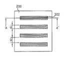
パターン化された前記導電性フィルム300において、隣り合う2つの線の間隔Dは1μm〜1mmであり、線の幅dは1μm〜1mmである。 In the patterned
次に、図5〜図8を参照しながら、本発明の第二実施例に係る導電板について説明する。 Next, a conductive plate according to a second embodiment of the present invention will be described with reference to FIGS.
図5及び図6を参照すると、本実施例において、前記導電板の製造方法の第一工程では、基板100及び接着層200を提供する。前記接着層200は、前記基板100に形成される。本実施例に係る導電板の基板100及び接着層200は、前記第一実施例に係る導電板の基板100及び接着層200と同じであるため、詳細な説明は省略する。 Referring to FIGS. 5 and 6, in this embodiment, the
前記導電板の製造方法の第二工程では、前記接着層200に対してパターン化処理を実施する。前記パターン化処理では、凹凸形成転写法、湿式エッチング法、乾式エッチング法、レーザーパターン化方法、刮除法又はテープ剥離除去法等を採用する。 In the second step of the method for manufacturing the conductive plate, a patterning process is performed on the
本実施例において、前記刮除法とは、ナイフのような工具で前記接着層200の不必要な部分を直接彫って除去して、前記接着層200をパターン化する方法を指す。前記テープ剥離除去法とは、前記接着層200の不必要な部分にテープを密着させた後、前記テープを剥離することで前記不必要な部分を除去して、前記接着層200をパターン化する方法を指す。レーザーパターン化法とは、レーザーで前記接着層200の不必要な部分を照射して、レーザーによる熱で前記不必要な部分を除去して、前記接着層200をパターン化する方法を指す。湿式エッチング法及び乾式エッチング法とは、いずれも平版印刷法で前記接着層200に、必要なパターンに沿って耐蝕剤を印刷した後、それぞれ液体エッチング又はイオン衝撃方式でパターン化に不必要な部分(耐蝕剤が印刷されない部分)を除去して、前記接着層200をパターン化する方法を指す。凹凸形成転写法とは、金型を利用して、前記接着層200の表面に必要なパターンを形成する方法を指す。また、本実施例におけるパターン化処理は、上述した方法のみに限定されるのではなく、他の方法によってパターン化処理されることもできる。 In this embodiment, the removal method refers to a method of patterning the
前記導電板の製造方法の第三工程では、導電性フィルム300を提供し、前記パターン化された接着層200を介して前記導電性フィルム300を前記基板100に接着させる。即ち、前記導電性フィルム300を前記接着層200の前記基板100に接触する表面と対向する表面に設置するため、前記接着層200は、前記導電性フィルム300と前記基板100との間に位置する。前記導電性フィルム300を前記パターン化されている接着剤層200に接着させた後、前記導電性フィルム300の未接着部分を切削などのような方式で除去する。 In the third step of the method for manufacturing the conductive plate, a
前記導電性フィルム300は、引張処理を実施することによって電気異方性を有することができる。また、前記導電性フィルム300は、複数のナノユニット(示せず)を含み、且つ前記複数のナノユニットを特定の方向に沿って配列させることにより、前記導電性フィルム300が電気異方性を有することになる。前記ナノユニットは、カーボンナノチューブ及びナノ粒子を含むことができる。電気異方性(導電異方性又は抵抗異方性とも称する)とは、異なる方向で異なる導電性(又は抵抗性)を有することを指す。 The
図7及び図8を参照すると、前記導電板の製造方法の第四工程では、導電材400を提供し、且つ前記導電材400を前記導電性フィルム300に電気接続させる。前記導電材400の一端は前記導電性フィルム300の上に位置し、前記導電材400の他端は前記基板100又は接着層200の上に位置する。前記導電材400は、導電性接着剤、導線、金属のような導電性材料によって形成される。前記導電性フィルム300は、電気異方性を有し、特定方向に沿ってその抵抗が小さく、前記特定方向と異なる方向に沿ってその抵抗が大きいので、前記導電材400を介して前記パターン化された導電性フィルム300を流れる電流を他の方向へガイドする。本実施例の導電板は、前記導電材400及びパターン化された前記導電性フィルム300によって、従来のITO層を含む導電板と同様な効果を奏することができる。 Referring to FIGS. 7 and 8, in a fourth step of the method for manufacturing the conductive plate, a
パターン化された前記導電性フィルム300において、隣り合う2つの線の間隔Dは1μm〜1mmであり、前記線の幅dは1μm〜1mmである。 In the patterned
本発明に係る導電板は、基板100と、前記基板100の1つの表面に形成されている接着層200と、前記接着層200の前記基板100に接触する表面と対向する表面に形成されている導電性フィルム300と、一端が前記導電性フィルム300に電気接続され、他端が前記基板100又は前記接着層200の上に位置する導電材400と、を備える。前記導電板において、前記接着層200又は前記導電性フィルム300に対してパターン化処理を実施する。 The conductive plate according to the present invention is formed on the
図9は、本発明の第一実施例に係るタッチパネルの構造を示す図である。 FIG. 9 is a diagram showing the structure of the touch panel according to the first embodiment of the present invention.
前記タッチパネルは、対向設置されている第一導電板600及び第二導電板700と、前記第一導電板600と前記第二導電板700との間に設置されている複数の絶縁素子500と、を備える。 The touch panel includes a first
前記第一導電板600は、第一基板610と、前記第一基板610の1つの表面に形成されている第一接着層620と、前記第一接着層620の前記第一基板610に接触する表面と対向する表面に形成されている第一導電性フィルム630と、一端が前記第一導電性フィルム630に電気接続され、他端が前記第一基板610又は前記第一接着層620の上に位置する第一導電材640と、を備える。前記第一導電板600において、前記第一接着層620又は前記第一導電性フィルム630は、第一パターン化処理されている。 The first
前記第二導電板700は、第二基板710と、前記第二基板710の1つの表面に形成されている第二接着層720と、前記第二接着層720の前記第二基板710に接触する表面と対向する表面に形成されている第二導電性フィルム730と、一端が前記第二導電性フィルム730に電気接続され、他端が前記第二基板710又は前記第二接着層720の上に位置する第二導電材740と、を備える。前記第二導電板700において、前記第二接着層720又は前記第二導電性フィルム730は、第二パターン化処理されている。 The second
本実施例において、前記第一導電板600及び前記第二導電板700は、いずれも上述した導電板の第二実施例の構造を採用したが、それに限定されるのではなく、いずれも上述した導電板の第一実施例の構造を採用することもできる。 In the present embodiment, the first
前記第一基板610及び前記第二基板710は前記基板100と同じであり、前記第一接着層620及び前記第二接着層720は前記接着層200と同じであり、前記第一導電性フィルム630及び前記第二導電性フィルム730は前記導電性フィルム300と同じであり、前記第一導電材640及び前記第二導電材740は前記導電材400と同じであるので、詳細な説明は省略する。 The
図10は、本発明の第二実施例に係るタッチパネルの構造を示す図である。 FIG. 10 is a diagram showing the structure of a touch panel according to the second embodiment of the present invention.
本実施例のタッチパネルの構造は、前記第一実施例に係るタッチパネルの構造と似ているが、本実施例の第一導電板600には、前記第一実施例に係る導電板を採用し、第二導電板700には、前記第二実施例に係る導電板を採用する点において、前記第一実施例に係るタッチパネルの構造と異なる。しかし、これに限定されるのではない。即ち、本実施例の第一導電板600には、前記第二実施例に係る導電板を採用し、第二導電板700には、前記第一実施例に係る導電板を採用することもできる。 The structure of the touch panel of the present embodiment is similar to the structure of the touch panel according to the first embodiment, but the first
本発明に係るタッチパネルを応用する場合、使用者は指、タッチペン又は他の部品で前記第二導電板700のある位置を接触すれば、接触位置で前記第二導電性フィルム730と前記第一導電性フィルム630とが電気接続されて、前記接触位置に電位差が発生し、外部の駆動素子は前記電位差を検知して接触位置の座標を計算し、前記タッチパネルの接触部位にカーソル(Cursor)を表示する。 When the touch panel according to the present invention is applied, if the user touches a certain position of the second
本発明に係る導電板において、接着層又は導電性フィルムに対してパターン化処理を実施して、導電性フィルムに感知線路を形成することにより、前記導電板の製造コストが下げることが可能である。 In the conductive plate according to the present invention, it is possible to reduce the manufacturing cost of the conductive plate by patterning the adhesive layer or the conductive film to form a sensing line on the conductive film. .
以上、本発明の好適な実施例について詳細に説明したが、本発明は前記実施例に限定されるものではなく、本発明の範囲内で種々の変形又は修正が可能であり、該変形又は修正も又、本発明の特許請求の範囲内に含まれるものであることは、いうまでもない。 The preferred embodiments of the present invention have been described in detail above. However, the present invention is not limited to the above-described embodiments, and various modifications or corrections are possible within the scope of the present invention. Needless to say, it is also included in the scope of the claims of the present invention.
100 基板
200 接着層
300 導電性フィルム
400 導電材
500 絶縁素子
600 第一導電板
610 第一基板
620 第一接着層
630 第一導電性フィルム
640 第一導電材
700 第二導電板
710 第二基板
720 第二接着層
730 第二導電性フィルム
740 第二導電材DESCRIPTION OF
Claims (19)
Translated fromJapanese前記導電性フィルム又は前記接着層が、パターン化処理されていることを特徴とする導電板。In a conductive plate comprising: a substrate; an adhesive layer formed on one surface of the substrate; and a conductive film formed on a surface of the adhesive layer that faces the surface that contacts the substrate.
The conductive plate, wherein the conductive film or the adhesive layer is patterned.
第二基板と、前記第二基板の1つの表面に形成されている第二接着層と、前記第二接着層の前記第二基板に接触する表面と対向する表面に形成され且つ前記第一導電性フィルムに対向して設置される第二導電性フィルムと、を含む第二導電板と、
を備えてなるタッチパネルにおいて、
前記第一接着層又は前記第一導電性フィルムが、第一パターン化処理されており、前記第二接着層又は前記第二導電性フィルムが、第二パターン化処理されていることを特徴とするタッチパネル。A first substrate, a first adhesive layer formed on one surface of the first substrate, and a first conductive layer formed on a surface of the first adhesive layer facing the surface contacting the first substrate. A first conductive plate including a conductive film;
A second substrate; a second adhesive layer formed on one surface of the second substrate; and a surface of the second adhesive layer facing the surface contacting the second substrate and the first conductive layer. A second conductive film including a second conductive film installed opposite to the conductive film,
In a touch panel comprising:
The first adhesive layer or the first conductive film is subjected to a first patterning process, and the second adhesive layer or the second conductive film is subjected to a second patterning process. Touch panel.
Applications Claiming Priority (2)
| Application Number | Priority Date | Filing Date | Title |
|---|---|---|---|
| CN2009103041322ACN101943963A (en) | 2009-07-08 | 2009-07-08 | Conducting plate and touch screen using same |
| CN200910304132.2 | 2009-07-08 |
Publications (2)
| Publication Number | Publication Date |
|---|---|
| JP2011018326Atrue JP2011018326A (en) | 2011-01-27 |
| JP5645512B2 JP5645512B2 (en) | 2014-12-24 |
Family
ID=42397700
Family Applications (1)
| Application Number | Title | Priority Date | Filing Date |
|---|---|---|---|
| JP2010153007AExpired - Fee RelatedJP5645512B2 (en) | 2009-07-08 | 2010-07-05 | Conductive plate and touch panel using the same |
Country Status (5)
| Country | Link |
|---|---|
| US (1) | US20110005815A1 (en) |
| EP (1) | EP2273354A1 (en) |
| JP (1) | JP5645512B2 (en) |
| KR (1) | KR20110004781A (en) |
| CN (1) | CN101943963A (en) |
Families Citing this family (11)
| Publication number | Priority date | Publication date | Assignee | Title |
|---|---|---|---|---|
| CN102221948A (en)* | 2011-05-11 | 2011-10-19 | 深圳市骏达光电有限公司 | Capacitive touch screen |
| TW201250967A (en)* | 2011-06-09 | 2012-12-16 | Shih Hua Technology Ltd | Touch panel and touch screen |
| CN102819338A (en)* | 2011-06-09 | 2012-12-12 | 天津富纳源创科技有限公司 | Production method of touch panel |
| CN102819340B (en)* | 2011-06-09 | 2016-03-02 | 天津富纳源创科技有限公司 | The preparation method of touch panel |
| CN102819341B (en)* | 2011-06-09 | 2016-02-24 | 天津富纳源创科技有限公司 | The preparation method of touch panel |
| KR101895416B1 (en) | 2011-12-23 | 2018-09-06 | 엘지이노텍 주식회사 | Print circuit board substrate and method ofmanufacturing the same |
| CN102929450A (en)* | 2012-11-21 | 2013-02-13 | 南京华显高科有限公司 | Preparation method for peelable glue protection graph of capacitive touch screen |
| CN105006272A (en)* | 2015-08-03 | 2015-10-28 | 佛山市顺德区百锐新电子材料有限公司 | Ultraviolet conductive silver slurry, and preparation method and application thereof |
| WO2017112438A1 (en)* | 2015-12-22 | 2017-06-29 | 3M Innovative Properties Company | Bonding layer having discrete adhesive patches |
| KR102710915B1 (en)* | 2016-10-25 | 2024-09-26 | 엘지디스플레이 주식회사 | Imprint mold and manufacturing method thereof |
| US10367333B2 (en)* | 2017-04-13 | 2019-07-30 | Nokia Of America Corporation | Increasing fabry-perot cavity free spectral range in hybrid lasers |
Citations (4)
| Publication number | Priority date | Publication date | Assignee | Title |
|---|---|---|---|---|
| JPH10246605A (en)* | 1997-03-05 | 1998-09-14 | Kanto Bussan Kk | Pressure sensitive input panel sensor |
| JP2003015286A (en)* | 2001-06-28 | 2003-01-15 | Tdk Corp | Substrate where functional layer pattern is formed and method for forming functional layer pattern |
| US20090046073A1 (en)* | 2007-08-14 | 2009-02-19 | Tyco Electronics Corporation | Touchscreen using both carbon nanoparticles and metal nanoparticles |
| JP2009104927A (en)* | 2007-10-24 | 2009-05-14 | Touch Panel Kenkyusho:Kk | Composite film or composite sheet transparent and with conductivity, and resistance film type touch panel structure |
Family Cites Families (10)
| Publication number | Priority date | Publication date | Assignee | Title |
|---|---|---|---|---|
| US5909083A (en)* | 1996-02-16 | 1999-06-01 | Dai Nippon Printing Co., Ltd. | Process for producing plasma display panel |
| JP3679943B2 (en)* | 1999-03-02 | 2005-08-03 | 大日本印刷株式会社 | Method for producing pattern forming body |
| TWI223116B (en)* | 2000-09-19 | 2004-11-01 | Au Optronics Corp | Liquid crystal display (LCD) device with a built-in touch panel and the manufacturing process thereof |
| KR100590727B1 (en)* | 2004-02-24 | 2006-06-19 | 한국기계연구원 | Microcontact Printing Technique Using Imprinted Nanostructures and Their Nanostructures |
| JP4657685B2 (en)* | 2004-11-11 | 2011-03-23 | 日立エーアイシー株式会社 | Method for manufacturing electromagnetic shielding film and film thereof |
| JP2006332592A (en)* | 2005-04-28 | 2006-12-07 | Ricoh Co Ltd | Electrical component, method for forming conductive pattern, and inkjet head |
| EP2053495A3 (en)* | 2007-10-23 | 2011-04-27 | Tsinghua University | Touch panel, method for making the same, and display device adopting the same |
| CN101458603B (en)* | 2007-12-12 | 2011-06-08 | 北京富纳特创新科技有限公司 | Touch screen and display device |
| WO2010001591A1 (en)* | 2008-07-04 | 2010-01-07 | 戸田工業株式会社 | Transparent electrically conductive transfer plate and production method therefor, transparent electrically conductive base, method for producing transparent electrically conductive base using transparent electrically conductive transfer plate, and molded article using transparent electrically conductive base |
| KR101316977B1 (en)* | 2008-08-22 | 2013-10-11 | 히타치가세이가부시끼가이샤 | Photosensitive conductive film, method for forming conductive film, method for forming conductive pattern, and conductive film substrate |
- 2009
- 2009-07-08CNCN2009103041322Apatent/CN101943963A/enactivePending
- 2010
- 2010-06-23USUS12/821,140patent/US20110005815A1/ennot_activeAbandoned
- 2010-06-30KRKR1020100062728Apatent/KR20110004781A/ennot_activeWithdrawn
- 2010-07-05JPJP2010153007Apatent/JP5645512B2/ennot_activeExpired - Fee Related
- 2010-07-07EPEP10168767Apatent/EP2273354A1/ennot_activeWithdrawn
Patent Citations (5)
| Publication number | Priority date | Publication date | Assignee | Title |
|---|---|---|---|---|
| JPH10246605A (en)* | 1997-03-05 | 1998-09-14 | Kanto Bussan Kk | Pressure sensitive input panel sensor |
| JP2003015286A (en)* | 2001-06-28 | 2003-01-15 | Tdk Corp | Substrate where functional layer pattern is formed and method for forming functional layer pattern |
| US20090046073A1 (en)* | 2007-08-14 | 2009-02-19 | Tyco Electronics Corporation | Touchscreen using both carbon nanoparticles and metal nanoparticles |
| JP2010537274A (en)* | 2007-08-14 | 2010-12-02 | タイコ・エレクトロニクス・コーポレイション | Touch screen using both carbon and metal nanoparticles |
| JP2009104927A (en)* | 2007-10-24 | 2009-05-14 | Touch Panel Kenkyusho:Kk | Composite film or composite sheet transparent and with conductivity, and resistance film type touch panel structure |
Also Published As
| Publication number | Publication date |
|---|---|
| KR20110004781A (en) | 2011-01-14 |
| US20110005815A1 (en) | 2011-01-13 |
| CN101943963A (en) | 2011-01-12 |
| EP2273354A1 (en) | 2011-01-12 |
| JP5645512B2 (en) | 2014-12-24 |
Similar Documents
| Publication | Publication Date | Title |
|---|---|---|
| JP5645512B2 (en) | Conductive plate and touch panel using the same | |
| TWI395998B (en) | Conductive plate and touch plate applied by the same | |
| JP4794392B2 (en) | Touch panel with curved surface and method for manufacturing the same | |
| US10452219B2 (en) | Touch sensor | |
| US20130044384A1 (en) | Color filter substrate embedded with touch sensor and method for manufacturing the same | |
| JP2013058184A (en) | Method for manufacturing touch panel | |
| US20110050636A1 (en) | Input device and display device provided with the same | |
| KR20120014302A (en) | Capacitive touch panel and its manufacturing method | |
| US20130075266A1 (en) | Method of manufacturing touch panel | |
| US8968506B2 (en) | Method for making touch panel | |
| JP2013122745A (en) | Touch panel and manufacturing method thereof | |
| KR20130023663A (en) | Method of manufacturing touch panel | |
| TW201439875A (en) | Touch panel and touch device with the same | |
| KR20130023665A (en) | Method of manufacturing touch panel | |
| US20150227170A1 (en) | Touch sensor and method for manufacturing the same | |
| KR20160089017A (en) | Touch panel and method of manufacturing the same | |
| JP2013084239A (en) | Touch panel and method of manufacturing the same | |
| TWI650777B (en) | Method for forming a line on a conductive polymer and a flexible touch device | |
| TWM488681U (en) | Touch panel | |
| US8883248B2 (en) | Method for making touch panel | |
| TW201530386A (en) | Touch sensor | |
| JP2014120149A (en) | Touch panel | |
| US20150103262A1 (en) | Touchscreen panel and manufacturing method thereof | |
| KR20130107682A (en) | Touch panel | |
| US8623163B2 (en) | Method for making touch panel |
Legal Events
| Date | Code | Title | Description |
|---|---|---|---|
| A621 | Written request for application examination | Free format text:JAPANESE INTERMEDIATE CODE: A621 Effective date:20130617 | |
| A977 | Report on retrieval | Free format text:JAPANESE INTERMEDIATE CODE: A971007 Effective date:20140221 | |
| A131 | Notification of reasons for refusal | Free format text:JAPANESE INTERMEDIATE CODE: A131 Effective date:20140224 | |
| A521 | Request for written amendment filed | Free format text:JAPANESE INTERMEDIATE CODE: A523 Effective date:20140522 | |
| TRDD | Decision of grant or rejection written | ||
| A01 | Written decision to grant a patent or to grant a registration (utility model) | Free format text:JAPANESE INTERMEDIATE CODE: A01 Effective date:20141006 | |
| A61 | First payment of annual fees (during grant procedure) | Free format text:JAPANESE INTERMEDIATE CODE: A61 Effective date:20141104 | |
| R150 | Certificate of patent or registration of utility model | Ref document number:5645512 Country of ref document:JP Free format text:JAPANESE INTERMEDIATE CODE: R150 | |
| R250 | Receipt of annual fees | Free format text:JAPANESE INTERMEDIATE CODE: R250 | |
| R250 | Receipt of annual fees | Free format text:JAPANESE INTERMEDIATE CODE: R250 | |
| LAPS | Cancellation because of no payment of annual fees |