JP2011014884A - Photoelectric conversion device - Google Patents
Photoelectric conversion deviceDownload PDFInfo
- Publication number
- JP2011014884A JP2011014884AJP2010122394AJP2010122394AJP2011014884AJP 2011014884 AJP2011014884 AJP 2011014884AJP 2010122394 AJP2010122394 AJP 2010122394AJP 2010122394 AJP2010122394 AJP 2010122394AJP 2011014884 AJP2011014884 AJP 2011014884A
- Authority
- JP
- Japan
- Prior art keywords
- semiconductor layer
- electrode
- aluminum
- photoelectric conversion
- conductive
- Prior art date
- Legal status (The legal status is an assumption and is not a legal conclusion. Google has not performed a legal analysis and makes no representation as to the accuracy of the status listed.)
- Withdrawn
Links
Images


Classifications
- H—ELECTRICITY
- H10—SEMICONDUCTOR DEVICES; ELECTRIC SOLID-STATE DEVICES NOT OTHERWISE PROVIDED FOR
- H10F—INORGANIC SEMICONDUCTOR DEVICES SENSITIVE TO INFRARED RADIATION, LIGHT, ELECTROMAGNETIC RADIATION OF SHORTER WAVELENGTH OR CORPUSCULAR RADIATION
- H10F71/00—Manufacture or treatment of devices covered by this subclass
- H10F71/138—Manufacture of transparent electrodes, e.g. transparent conductive oxides [TCO] or indium tin oxide [ITO] electrodes
- C—CHEMISTRY; METALLURGY
- C23—COATING METALLIC MATERIAL; COATING MATERIAL WITH METALLIC MATERIAL; CHEMICAL SURFACE TREATMENT; DIFFUSION TREATMENT OF METALLIC MATERIAL; COATING BY VACUUM EVAPORATION, BY SPUTTERING, BY ION IMPLANTATION OR BY CHEMICAL VAPOUR DEPOSITION, IN GENERAL; INHIBITING CORROSION OF METALLIC MATERIAL OR INCRUSTATION IN GENERAL
- C23C—COATING METALLIC MATERIAL; COATING MATERIAL WITH METALLIC MATERIAL; SURFACE TREATMENT OF METALLIC MATERIAL BY DIFFUSION INTO THE SURFACE, BY CHEMICAL CONVERSION OR SUBSTITUTION; COATING BY VACUUM EVAPORATION, BY SPUTTERING, BY ION IMPLANTATION OR BY CHEMICAL VAPOUR DEPOSITION, IN GENERAL
- C23C14/00—Coating by vacuum evaporation, by sputtering or by ion implantation of the coating forming material
- C23C14/06—Coating by vacuum evaporation, by sputtering or by ion implantation of the coating forming material characterised by the coating material
- C23C14/0676—Oxynitrides
- H—ELECTRICITY
- H10—SEMICONDUCTOR DEVICES; ELECTRIC SOLID-STATE DEVICES NOT OTHERWISE PROVIDED FOR
- H10F—INORGANIC SEMICONDUCTOR DEVICES SENSITIVE TO INFRARED RADIATION, LIGHT, ELECTROMAGNETIC RADIATION OF SHORTER WAVELENGTH OR CORPUSCULAR RADIATION
- H10F10/00—Individual photovoltaic cells, e.g. solar cells
- H10F10/10—Individual photovoltaic cells, e.g. solar cells having potential barriers
- H10F10/17—Photovoltaic cells having only PIN junction potential barriers
- H10F10/172—Photovoltaic cells having only PIN junction potential barriers comprising multiple PIN junctions, e.g. tandem cells
- H—ELECTRICITY
- H10—SEMICONDUCTOR DEVICES; ELECTRIC SOLID-STATE DEVICES NOT OTHERWISE PROVIDED FOR
- H10F—INORGANIC SEMICONDUCTOR DEVICES SENSITIVE TO INFRARED RADIATION, LIGHT, ELECTROMAGNETIC RADIATION OF SHORTER WAVELENGTH OR CORPUSCULAR RADIATION
- H10F10/00—Individual photovoltaic cells, e.g. solar cells
- H10F10/10—Individual photovoltaic cells, e.g. solar cells having potential barriers
- H10F10/17—Photovoltaic cells having only PIN junction potential barriers
- H10F10/174—Photovoltaic cells having only PIN junction potential barriers comprising monocrystalline or polycrystalline materials
- H—ELECTRICITY
- H10—SEMICONDUCTOR DEVICES; ELECTRIC SOLID-STATE DEVICES NOT OTHERWISE PROVIDED FOR
- H10F—INORGANIC SEMICONDUCTOR DEVICES SENSITIVE TO INFRARED RADIATION, LIGHT, ELECTROMAGNETIC RADIATION OF SHORTER WAVELENGTH OR CORPUSCULAR RADIATION
- H10F19/00—Integrated devices, or assemblies of multiple devices, comprising at least one photovoltaic cell covered by group H10F10/00, e.g. photovoltaic modules
- H10F19/30—Integrated devices, or assemblies of multiple devices, comprising at least one photovoltaic cell covered by group H10F10/00, e.g. photovoltaic modules comprising thin-film photovoltaic cells
- H10F19/31—Integrated devices, or assemblies of multiple devices, comprising at least one photovoltaic cell covered by group H10F10/00, e.g. photovoltaic modules comprising thin-film photovoltaic cells having multiple laterally adjacent thin-film photovoltaic cells deposited on the same substrate
- H10F19/33—Patterning processes to connect the photovoltaic cells, e.g. laser cutting of conductive or active layers
- H—ELECTRICITY
- H10—SEMICONDUCTOR DEVICES; ELECTRIC SOLID-STATE DEVICES NOT OTHERWISE PROVIDED FOR
- H10F—INORGANIC SEMICONDUCTOR DEVICES SENSITIVE TO INFRARED RADIATION, LIGHT, ELECTROMAGNETIC RADIATION OF SHORTER WAVELENGTH OR CORPUSCULAR RADIATION
- H10F19/00—Integrated devices, or assemblies of multiple devices, comprising at least one photovoltaic cell covered by group H10F10/00, e.g. photovoltaic modules
- H10F19/30—Integrated devices, or assemblies of multiple devices, comprising at least one photovoltaic cell covered by group H10F10/00, e.g. photovoltaic modules comprising thin-film photovoltaic cells
- H10F19/31—Integrated devices, or assemblies of multiple devices, comprising at least one photovoltaic cell covered by group H10F10/00, e.g. photovoltaic modules comprising thin-film photovoltaic cells having multiple laterally adjacent thin-film photovoltaic cells deposited on the same substrate
- H10F19/35—Structures for the connecting of adjacent photovoltaic cells, e.g. interconnections or insulating spacers
- H—ELECTRICITY
- H10—SEMICONDUCTOR DEVICES; ELECTRIC SOLID-STATE DEVICES NOT OTHERWISE PROVIDED FOR
- H10F—INORGANIC SEMICONDUCTOR DEVICES SENSITIVE TO INFRARED RADIATION, LIGHT, ELECTROMAGNETIC RADIATION OF SHORTER WAVELENGTH OR CORPUSCULAR RADIATION
- H10F71/00—Manufacture or treatment of devices covered by this subclass
- H10F71/10—Manufacture or treatment of devices covered by this subclass the devices comprising amorphous semiconductor material
- H10F71/103—Manufacture or treatment of devices covered by this subclass the devices comprising amorphous semiconductor material including only Group IV materials
- H—ELECTRICITY
- H10—SEMICONDUCTOR DEVICES; ELECTRIC SOLID-STATE DEVICES NOT OTHERWISE PROVIDED FOR
- H10F—INORGANIC SEMICONDUCTOR DEVICES SENSITIVE TO INFRARED RADIATION, LIGHT, ELECTROMAGNETIC RADIATION OF SHORTER WAVELENGTH OR CORPUSCULAR RADIATION
- H10F77/00—Constructional details of devices covered by this subclass
- H10F77/20—Electrodes
- H10F77/244—Electrodes made of transparent conductive layers, e.g. transparent conductive oxide [TCO] layers
- H10F77/251—Electrodes made of transparent conductive layers, e.g. transparent conductive oxide [TCO] layers comprising zinc oxide [ZnO]
- Y—GENERAL TAGGING OF NEW TECHNOLOGICAL DEVELOPMENTS; GENERAL TAGGING OF CROSS-SECTIONAL TECHNOLOGIES SPANNING OVER SEVERAL SECTIONS OF THE IPC; TECHNICAL SUBJECTS COVERED BY FORMER USPC CROSS-REFERENCE ART COLLECTIONS [XRACs] AND DIGESTS
- Y02—TECHNOLOGIES OR APPLICATIONS FOR MITIGATION OR ADAPTATION AGAINST CLIMATE CHANGE
- Y02E—REDUCTION OF GREENHOUSE GAS [GHG] EMISSIONS, RELATED TO ENERGY GENERATION, TRANSMISSION OR DISTRIBUTION
- Y02E10/00—Energy generation through renewable energy sources
- Y02E10/50—Photovoltaic [PV] energy
- Y02E10/547—Monocrystalline silicon PV cells
- Y—GENERAL TAGGING OF NEW TECHNOLOGICAL DEVELOPMENTS; GENERAL TAGGING OF CROSS-SECTIONAL TECHNOLOGIES SPANNING OVER SEVERAL SECTIONS OF THE IPC; TECHNICAL SUBJECTS COVERED BY FORMER USPC CROSS-REFERENCE ART COLLECTIONS [XRACs] AND DIGESTS
- Y02—TECHNOLOGIES OR APPLICATIONS FOR MITIGATION OR ADAPTATION AGAINST CLIMATE CHANGE
- Y02E—REDUCTION OF GREENHOUSE GAS [GHG] EMISSIONS, RELATED TO ENERGY GENERATION, TRANSMISSION OR DISTRIBUTION
- Y02E10/00—Energy generation through renewable energy sources
- Y02E10/50—Photovoltaic [PV] energy
- Y02E10/548—Amorphous silicon PV cells
- Y—GENERAL TAGGING OF NEW TECHNOLOGICAL DEVELOPMENTS; GENERAL TAGGING OF CROSS-SECTIONAL TECHNOLOGIES SPANNING OVER SEVERAL SECTIONS OF THE IPC; TECHNICAL SUBJECTS COVERED BY FORMER USPC CROSS-REFERENCE ART COLLECTIONS [XRACs] AND DIGESTS
- Y02—TECHNOLOGIES OR APPLICATIONS FOR MITIGATION OR ADAPTATION AGAINST CLIMATE CHANGE
- Y02P—CLIMATE CHANGE MITIGATION TECHNOLOGIES IN THE PRODUCTION OR PROCESSING OF GOODS
- Y02P70/00—Climate change mitigation technologies in the production process for final industrial or consumer products
- Y02P70/50—Manufacturing or production processes characterised by the final manufactured product
Landscapes
- Chemical & Material Sciences (AREA)
- Chemical Kinetics & Catalysis (AREA)
- Engineering & Computer Science (AREA)
- Materials Engineering (AREA)
- Mechanical Engineering (AREA)
- Metallurgy (AREA)
- Organic Chemistry (AREA)
- Photovoltaic Devices (AREA)
- Electrodes Of Semiconductors (AREA)
- Physical Vapour Deposition (AREA)
Abstract
Translated fromJapaneseDescription
Translated fromJapanese本発明の一態様は、半導体の光起電力効果を利用する光電変換装置に関する。開示される一態様には透光性導電膜を用いた光電変換装置が含まれる。One embodiment of the present invention relates to a photoelectric conversion device using a photovoltaic effect of a semiconductor. One embodiment disclosed includes a photoelectric conversion device using a light-transmitting conductive film.
半導体薄膜を用いて構成する光電変換装置では、その構成の一部に透光性導電膜が用いられている。例えば、光電変換装置の光入射側の電極として、或いはタンデム型光電変換装置の上部光電変換セルと下部光電変換セルとの間に設ける中間導電層として、さらには光電変換装置の裏面側に設けられる反射電極と半導体層との間の導電層として用いられている(例えば、特許文献1、2参照)。In a photoelectric conversion device configured using a semiconductor thin film, a translucent conductive film is used as part of the configuration. For example, as an electrode on the light incident side of the photoelectric conversion device, or as an intermediate conductive layer provided between the upper photoelectric conversion cell and the lower photoelectric conversion cell of the tandem photoelectric conversion device, and further provided on the back side of the photoelectric conversion device. It is used as a conductive layer between the reflective electrode and the semiconductor layer (see, for example,
光電変換装置に用いられる透光性導電膜として、酸化インジウムに酸化スズを添加して焼結したターゲットを用いて成膜した酸化インジウム−酸化スズ化合物(In2O3―SnO2、以下「ITO」と略記する。)膜や酸化スズが従来から用いられている。As a translucent conductive film used in a photoelectric conversion device, an indium oxide-tin oxide compound (In2 O3 —SnO2) formed using a target obtained by adding tin oxide to indium oxide and sintering it, hereinafter referred to as “ITO” Abbreviated as “). Films and tin oxide have been used conventionally.
ITOは、他の材料系の透光性導電膜と比較して抵抗率が低く、可視光領域での透明性が高いという特性がある。その一方、ITOの主材料であるインジウムは、レアメタルであるため価格が高く、産出国も限られるため、工業的に広く利用されつつも課題が内在している。ITO has characteristics that its resistivity is low and transparency in the visible light region is high as compared with light-transmitting conductive films of other material systems. On the other hand, indium, which is the main material of ITO, is a rare metal and is expensive, and the country of production is limited. Therefore, the problem is inherent while being widely used industrially.
酸化スズは抵抗率がITOと比較して高く、厚膜化しなければならないこと、及び光電変換装置に適した膜と作製するには基板温度を高温化する必要がある(例えば、特許文献3参照)。Tin oxide has a higher resistivity than ITO and must be made thicker, and it is necessary to increase the substrate temperature to produce a film suitable for a photoelectric conversion device (see, for example, Patent Document 3). ).
その他の透光性導電膜として酸化亜鉛が知られている。酸化亜鉛は透明性及び導電性においては、ITOに劣るとされるが、ITOと比較して非常に安価な材料である。例えば、酸化亜鉛を焼結したターゲットのコストは、ITOを焼結させたターゲットのコストの2/3〜1/2程度である。また、酸化亜鉛の導電性を向上させるために、ドナーとして機能する微量のアルミニウムを酸化亜鉛に含ませて透光性導電性酸化物を形成する方法が知られている(特許文献4参照)。Zinc oxide is known as another translucent conductive film. Zinc oxide is considered to be inferior to ITO in transparency and conductivity, but is a very inexpensive material compared to ITO. For example, the cost of the target sintered with zinc oxide is about 2/3 to 1/2 of the cost of the target sintered with ITO. Moreover, in order to improve the electroconductivity of zinc oxide, the method of forming a translucent conductive oxide by including in a zinc oxide a trace amount aluminum which functions as a donor is known (refer patent document 4).
しかしながら、従来の酸化亜鉛膜は、耐薬品性がなくアルカリ溶液に可溶であり、耐湿性が悪く抵抗率が増加してしまうという問題がある。そのため、光電変換装置の透光性導電膜として用いても、特性の向上や安定化を図れないといった問題がある。However, the conventional zinc oxide film has a problem that it has no chemical resistance and is soluble in an alkaline solution, and has poor moisture resistance and an increased resistivity. Therefore, there is a problem that characteristics cannot be improved or stabilized even when used as a translucent conductive film of a photoelectric conversion device.
本発明の一態様は、安価な酸化亜鉛材料を光電変換装置の透光性導電膜として用いることのできる技術を提供することを目的の一とする。An object of one embodiment of the present invention is to provide a technique in which an inexpensive zinc oxide material can be used as a light-transmitting conductive film of a photoelectric conversion device.
本発明の一形態は、第1電極と第2電極との間に、一導電型である第1不純物半導体層と、半導体層と、第1不純物半導体層と逆導電型である第2不純物半導体層とが順に積層されて半導体接合を構成するユニットセルを1つ以上含み、第1の電極または第2の電極は、亜鉛及びアルミニウムを含む導電性酸窒化物で形成される光電変換装置である。According to one embodiment of the present invention, a first impurity semiconductor layer having one conductivity type, a semiconductor layer, and a second impurity semiconductor having a conductivity type opposite to that of the first impurity semiconductor layer are provided between the first electrode and the second electrode. The photoelectric conversion device includes one or more unit cells that are stacked in order to form a semiconductor junction, and the first electrode or the second electrode is formed of a conductive oxynitride containing zinc and aluminum. .
また、本発明の一形態は、第1電極と、第1電極上に形成される第1のユニットセルと、第1のユニットセル上に形成される中間導電層と、中間導電層上に形成される第2のユニットセルと、第2のユニットセル上に形成される第2の電極とを有し、第1のユニットセルは、一導電型である第1不純物半導体層と、第1の半導体層と、第1不純物半導体層と逆導電型である第2不純物半導体層とが順に積層されて半導体接合を構成し、第2のユニットセルは、一導電型である第3不純物半導体層と、第2の半導体層と、第3不純物半導体層と逆導電型である第4不純物半導体層とが順に積層されて半導体接合を構成し、第1の電極、第2の電極、または中間導電層は、亜鉛及びアルミニウムを含む導電性酸窒化物で形成される光電変換装置である。In one embodiment of the present invention, a first electrode, a first unit cell formed over the first electrode, an intermediate conductive layer formed over the first unit cell, and an intermediate conductive layer are formed. The second unit cell, and a second electrode formed on the second unit cell, the first unit cell including a first impurity semiconductor layer of one conductivity type, A semiconductor layer and a first impurity semiconductor layer and a second impurity semiconductor layer having a conductivity type opposite to each other are sequentially stacked to form a semiconductor junction, and the second unit cell includes a third impurity semiconductor layer having a conductivity type, The second semiconductor layer and the fourth impurity semiconductor layer having a conductivity type opposite to that of the third impurity semiconductor layer are sequentially stacked to form a semiconductor junction, and the first electrode, the second electrode, or the intermediate conductive layer Is a photoelectric conversion device formed of conductive oxynitride containing zinc and aluminum That.
なお、亜鉛及びアルミニウムを含む導電性酸窒化物は、亜鉛の組成比が47原子%以下であり且つ前記アルミニウムの組成比より大きく、アルミニウムの組成比は窒素の組成比より大きく、二次イオン質量分析法により測定される前記窒素の濃度は、5.0×10²⁰atoms/cm3以上である。または、亜鉛及びアルミニウムを含む導電性酸窒化物は、亜鉛の組成比が47原子%以下であり、且つアルミニウムの組成比より大きく、アルミニウムの組成比は窒素の組成比より大きく、1.0原子%乃至8.0原子%の前記アルミニウムを含み、且つ0.5原子%乃至4.0原子%の窒素を含む。Note that the conductive oxynitride containing zinc and aluminum has a zinc composition ratio of 47 atomic% or less and larger than the aluminum composition ratio, and the aluminum composition ratio is larger than the nitrogen composition ratio and the secondary ion mass. The nitrogen concentration measured by the analysis method is 5.0 × 10²⁰ atoms / cm3 or more. Alternatively, the conductive oxynitride containing zinc and aluminum has a zinc composition ratio of 47 atomic percent or less and larger than the aluminum composition ratio, and the aluminum composition ratio is larger than the nitrogen composition ratio and 1.0 atom. % To 8.0 atomic% of the aluminum, and 0.5 atomic% to 4.0 atomic% of nitrogen.
なお、本明細書における窒素濃度、酸素濃度、および炭素濃度は、二次イオン質量分析法(SIMS;Secondary Ion Mass Spectrometer)によって計測されるピーク値の濃度である。また、亜鉛及びアルミニウムを含む導電性酸窒化物の組成比の単位は原子%とし、電子線マイクロアナライザー(EPMA:Electron Probe X−ray MicroAnalyzer)を用いた分析により評価するものとする。Note that the nitrogen concentration, the oxygen concentration, and the carbon concentration in this specification are concentrations of peak values measured by a secondary ion mass spectrometry (SIMS; Secondary Ion Mass Spectrometer). In addition, the unit of the composition ratio of the conductive oxynitride containing zinc and aluminum is atomic%, and the evaluation is performed by analysis using an electron beam microanalyzer (EPMA: Electron Probe X-ray MicroAnalyzer).
また、本明細書における非単結晶半導体とは、実質的に真性である半導体を範疇に含む。具体的には、非単結晶半導体に含まれるp型を付与する不純物(代表的にはボロン)若しくはn型を付与する不純物(代表的にはリン)が1×1018cm−3未満の濃度であり、暗伝導度に対して光伝導度が100倍以上である非単結晶半導体を指す。なお、非単結晶半導体は、価電子制御を目的とした不純物元素を意図的に添加しないときに弱いn型の電気伝導性を示す場合がある。そのため、非単結晶半導体の成膜中、或いは成膜後にp型を付与する不純物(代表的にはボロン)を添加することもある。このような場合、非単結晶半導体に含まれるp型不純物の濃度は概略1×10¹⁴/cm3〜6×1016/cm3である。In addition, the non-single-crystal semiconductor in this specification includes, in its category, a semiconductor that is substantially intrinsic. Specifically, the concentration of an impurity imparting p-type (typically boron) or an impurity imparting n-type (typically phosphorus) included in the non-single-crystal semiconductor is less than 1 × 1018 cm−3. It refers to a non-single-crystal semiconductor whose photoconductivity is 100 times or more of dark conductivity. Note that a non-single-crystal semiconductor may exhibit weak n-type conductivity when an impurity element for the purpose of controlling valence electrons is not intentionally added. Therefore, an impurity imparting p-type conductivity (typically boron) may be added during or after the formation of the non-single-crystal semiconductor. In such a case, the concentration of the p-type impurity contained in the non-single-crystal semiconductor is approximately 1 × 10¹⁴ / cm3 to 6 × 10¹⁶ / cm3 .
また、本明細書における「光電変換層」とは、光電効果(内部光電効果)を発現する半導体層を含む他、内部電界や半導体接合を形成するために接合された不純物半導体層を含めたものをいう。すなわち、本明細書における光電変換層は、pin接合などを代表例とする接合が形成された半導体層を示す。In addition, the “photoelectric conversion layer” in this specification includes a semiconductor layer that exhibits a photoelectric effect (internal photoelectric effect), and also includes an impurity semiconductor layer that is bonded to form an internal electric field or a semiconductor junction. Say. That is, the photoelectric conversion layer in this specification indicates a semiconductor layer in which a junction such as a pin junction is a representative example.
また、本明細書における「pin接合」は、光入射側からp型半導体層、i型半導体層、n型半導体層の積層順で配置されるものと、光入射側からn型半導体層、i型半導体層、p型半導体層の積層順で配置されるものを含むものとする。In addition, the “pin junction” in this specification refers to a layer in which the p-type semiconductor layer, the i-type semiconductor layer, and the n-type semiconductor layer are arranged in the order of lamination from the light incident side, and the n-type semiconductor layer, i from the light incident side. It includes a semiconductor layer disposed in the stacking order of a p-type semiconductor layer and a p-type semiconductor layer.
また、本明細書において、「第1」、「第2」、「第3」などの数詞の付く用語は、要素を区別するために便宜的に付与しているものである。したがって、数的に限定するものではなく、配置および段階の順序を限定するものでもない。Further, in this specification, terms having numerals such as “first”, “second”, and “third” are given for convenience in order to distinguish elements. Therefore, it is not limited numerically, nor does it limit the order of arrangement and steps.
良好な透光性及び導電性を有する透光性導電膜を低コストで形成することができ、これにより光電変換装置のコストを低減することができる。A light-transmitting conductive film having favorable light-transmitting properties and conductivity can be formed at low cost, whereby the cost of the photoelectric conversion device can be reduced.
また透光性導電膜の抵抗率を低減することができるので、光電流の取り出し効率を向上させることができる。In addition, since the resistivity of the light-transmitting conductive film can be reduced, the photocurrent extraction efficiency can be improved.
本発明の実施の形態について、図面を用いて以下に説明する。ただし、本発明は以下の説明に限定されず、本発明の趣旨およびその範囲から逸脱することなく、その形態および詳細をさまざまに変更しうることは当業者であれば容易に理解される。したがって、本発明は以下に示す実施の形態の記載内容に限定して解釈されるものではない。なお、以下に説明する本発明の構成において、同じものを指す符号は異なる図面間で共通して用いる。Embodiments of the present invention will be described below with reference to the drawings. However, the present invention is not limited to the following description, and it is easily understood by those skilled in the art that modes and details can be variously changed without departing from the spirit and scope of the present invention. Therefore, the present invention should not be construed as being limited to the description of the embodiments below. Note that in the structures of the present invention described below, the same reference numerals are used in common in different drawings.
(実施の形態1)
図1に、本実施の形態に係る光電変換装置100の断面模式図の一例を示す。(Embodiment 1)
FIG. 1 shows an example of a schematic cross-sectional view of a
図1に示す光電変換装置100は、基板101上に設けられた第1電極102と第2電極140との間に、ユニットセル110が挟持された構成を有する。ユニットセル110は、第1不純物半導体層112pと第2不純物半導体層116nとの間に半導体層114iが設けられており、少なくとも一つの半導体接合を含んでいる。半導体接合としては、代表的にはpin接合が挙げられる。A
第1電極102は、本実施の形態では基板101側を光入射側とするため、透光性を有する電極とする。本実施の形態では、第1電極102として、亜鉛(Zn)、アルミニウム(Al)、窒素(N)、酸素(O)を含む酸窒化物導電膜を用いる。このような酸窒化物導電膜を、「ZnOAlN」、「AZON」、或いは亜鉛及びアルミニウムを含む導電性酸窒化物と呼ぶこととする。ただし、「ZnOAlN」あるいは「AZON」は、ZnOAlNあるいはAZONに含まれる亜鉛(Zn)、アルミニウム(Al)、窒素(N)、酸素(O)の組成比を表すものではない。In this embodiment mode, the
本実施の形態における亜鉛及びアルミニウムを含む導電性酸窒化物とは、代表的には、亜鉛の組成比が47原子%以下であり、アルミニウムの組成比(原子%)より大きい。また、アルミニウムの組成比(原子%)は窒素の組成比より大きい。また、SIMSにより測定される窒素の濃度は、5.0×10²⁰atoms/cm3以上である導電性酸窒化物である。また、亜鉛及びアルミニウムを含む導電性酸窒化物は、少なくとも多結晶構造を有することが好ましい。The conductive oxynitride containing zinc and aluminum in this embodiment typically has a zinc composition ratio of 47 atomic% or less, which is larger than the aluminum composition ratio (atomic%). Moreover, the composition ratio (atomic%) of aluminum is larger than the composition ratio of nitrogen. Further, the nitrogen concentration measured by SIMS is a conductive oxynitride of 5.0 × 10²⁰ atoms / cm3 or more. The conductive oxynitride containing zinc and aluminum preferably has at least a polycrystalline structure.
ここで、亜鉛及びアルミニウムを含む導電性酸窒化物のキャリア密度は、1.0×1020cm−3乃至2.0×1021cm−3が好ましく、より好ましくは、2.2×1020cm−3以上4.2×1020cm−3未満とする。また、亜鉛及びアルミニウムを含む導電性酸窒化物の移動度は、4.0cm2/V・sec乃至60cm2/V・secが好ましく、より好ましくは、4.7cm2/V・sec以上36.0cm2/V・sec未満とする。また、亜鉛及びアルミニウムを含む導電性酸窒化物の抵抗率は、1.0×10−4Ω・cm乃至1.0×10−2Ω・cmが好ましく、より好ましくは、4.1×10−4Ω・cmより大きく、6.1×10−3Ω・cm以下とする。Here, the carrier density of the conductive oxynitride containing zinc and aluminum is preferably 1.0 × 1020 cm−3 to 2.0 × 1021 cm−3 , more preferably 2.2 × 10²⁰. cm−3 or more and less than 4.2 × 1020 cm−3 . Moreover, the mobility of the conductive oxynitride including zinc and aluminum is preferably 4.0cm2 / V · sec to 60cm2 / V · sec, more preferably, 4.7cm2 / V · sec or more 36. 0 cm2 / V · sec. The resistivity of the conductive oxynitride containing zinc and aluminum is preferably 1.0 × 10⁻⁴ Ω · cm to 1.0 × 10⁻² Ω · cm, more preferably 4.1 × 10.It is larger than−4 Ω · cm and not more than 6.1 × 10⁻³ Ω · cm.
また、厚さ100nm程度に形成された亜鉛及びアルミニウムを含む導電性酸窒化物の波長470nmの青色光の透過率は、0.70以上であることが好ましく、より好ましくは、0.75以上とする。また、厚さ100nm程度に形成された亜鉛及びアルミニウムを含む導電性酸窒化物の波長530nmの緑色光の透過率は、0.70以上であることが好ましく、より好ましくは、0.75以上とする。また、厚さ100nm程度に形成された亜鉛及びアルミニウムを含む導電性酸窒化物の波長680nmの赤色光の透過率は、0.70以上であることが好ましく、より好ましくは、0.75以上とする。なお、亜鉛及びアルミニウムを含む導電性酸窒化物は、以上の条件のうち少なくとも1つを満たすものとする。The transmittance of blue light with a wavelength of 470 nm of the conductive oxynitride containing zinc and aluminum formed to a thickness of about 100 nm is preferably 0.70 or more, more preferably 0.75 or more. To do. Further, the transmittance of green light having a wavelength of 530 nm of the conductive oxynitride containing zinc and aluminum formed to a thickness of about 100 nm is preferably 0.70 or more, more preferably 0.75 or more. To do. Further, the transmittance of red light having a wavelength of 680 nm of the conductive oxynitride containing zinc and aluminum formed to a thickness of about 100 nm is preferably 0.70 or more, more preferably 0.75 or more. To do. Note that the conductive oxynitride containing zinc and aluminum satisfies at least one of the above conditions.
また、亜鉛及びアルミニウムを含む導電性酸窒化物中の亜鉛の組成比(原子%)は、47原子%以下とし、アルミニウムの組成比(原子%)より大きい。また、アルミニウムの組成比(原子%)は、窒素の組成比(原子%)より大きい。また、亜鉛及びアルミニウムを含む導電性酸窒化物中には、1.0原子%乃至8.0原子%のアルミニウム及び0.5原子%乃至4.0原子%の窒素が含まれるのが好ましい。Further, the composition ratio (atomic%) of zinc in the conductive oxynitride containing zinc and aluminum is set to 47 atomic% or less, which is larger than the composition ratio (atomic%) of aluminum. Moreover, the composition ratio (atomic%) of aluminum is larger than the composition ratio (atomic%) of nitrogen. Further, the conductive oxynitride containing zinc and aluminum preferably contains 1.0 atomic% to 8.0 atomic% of aluminum and 0.5 atomic% to 4.0 atomic% of nitrogen.
以上のような組成となるように形成することによって、抵抗率の低減された亜鉛及びアルミニウムを含む導電性酸窒化物を作製することができる。なお、亜鉛及びアルミニウムを含む導電性酸窒化物の組成比の単位は原子%とし、電子線マイクロアナライザーを用いた分析により評価するものとする。By forming such a composition as described above, a conductive oxynitride containing zinc and aluminum with reduced resistivity can be manufactured. Note that the unit of the composition ratio of the conductive oxynitride containing zinc and aluminum is atomic%, and the evaluation is performed by analysis using an electron beam microanalyzer.
また、亜鉛及びアルミニウムを含む導電性酸窒化物は、少なくとも多結晶構造を有する。なお、導電性酸窒化物の結晶状態は、X線回折(XRD:X−ray diffraction)の分析により評価するものとする。The conductive oxynitride containing zinc and aluminum has at least a polycrystalline structure. Note that the crystalline state of the conductive oxynitride is evaluated by analysis of X-ray diffraction (XRD).
なお、第1電極102と基板101の間に、酸化インジウム、酸化インジウムスズ合金(ITO)、酸化亜鉛などの透光性の導電材料を用いて、透光性を有する電極を形成してもよい。Note that a light-transmitting electrode may be formed between the
半導体層114iは、単結晶半導体または非単結晶半導体を用いて形成する。The
半導体層114iに用いることが可能な非単結晶半導体層としては、非晶質半導体、微結晶半導体、または多結晶半導体がある。非晶質半導体の代表例としては、アモルファスシリコン、アモルファスシリコンゲルマニウム等がある。また、微結晶半導体、としては、微結晶シリコン、微結晶シリコンゲルマニウム等がある。また、多結晶半導体の代表例としては、ポリシリコン、ポリシリコンゲルマニウム等がある。As the non-single-crystal semiconductor layer that can be used for the
非晶質半導体(代表的にはアモルファスシリコン)のバンドギャップは1.6eV乃至1.8eVであり、多結晶半導体(代表的にはポリシリコン)のバンドギャップは1.1eV乃至1.4eV程度である。The band gap of an amorphous semiconductor (typically amorphous silicon) is 1.6 eV to 1.8 eV, and the band gap of a polycrystalline semiconductor (typically polysilicon) is about 1.1 eV to 1.4 eV. is there.
非単結晶半導体は、単結晶半導体よりもバンドギャップが広い。そのため、単結晶半導体により長波長域光を利用して発電することができ、非単結晶半導体により短波長域光を利用して発電することができる。太陽光は広範囲の波長帯域を有するため、非単結晶半導体を用いた場合には効率よく発電を行うことができる。A non-single crystal semiconductor has a wider band gap than a single crystal semiconductor. Therefore, it is possible to generate power using a long wavelength band light by a single crystal semiconductor, and to generate power using a short wavelength band light by a non-single crystal semiconductor. Since sunlight has a wide wavelength band, power can be generated efficiently when a non-single crystal semiconductor is used.
また、非単結晶半導体として、非晶質構造の中に結晶が離散的に存在している半導体を用いてもよい。当該結晶は、内部電界を形成するために接合された一対の不純物半導体層間、すなわちp型半導体層及びn型半導体層の間に連続的に存在して貫通するように成長していてもよい。Further, as the non-single-crystal semiconductor, a semiconductor in which crystals are discretely present in an amorphous structure may be used. The crystal may be grown so as to continuously exist between a pair of impurity semiconductor layers bonded to form an internal electric field, that is, between a p-type semiconductor layer and an n-type semiconductor layer.
非晶質構造の中に離散的に存在する結晶の形状は、針状であることが好ましい。ここで、「針状」とは、錐形状や柱状のものを含む。具体的には、円錐、円柱、角錐、または角柱などが挙げられる。角錐としては、三角錐、四角錐、六角錐などが挙げられ、角柱としては、三角柱、四角柱、六角柱などが挙げられる。もちろん、その他の多角錐形状または多角柱状のものでもよい。また、円錐状や角錐状で先端が平坦なもの、円柱状や角柱状で先端が尖っているものも含む。多角錐または多角柱の場合、多角形の各辺は等しくともよいし、異なる長さでもよい。The shape of the crystal discretely present in the amorphous structure is preferably a needle shape. Here, the “needle shape” includes a cone shape or a column shape. Specifically, a cone, a cylinder, a pyramid, a prism, or the like can be given. Examples of the pyramid include a triangular pyramid, a quadrangular pyramid, and a hexagonal pyramid. Examples of the prism include a triangular prism, a quadrangular prism, and a hexagonal prism. Of course, other polygonal pyramid shapes or polygonal columnar shapes may be used. Moreover, the thing with a flat tip | tip with a cone shape or a pyramid shape, and the shape with a cylindrical tip or a prismatic shape with a sharp tip are included. In the case of a polygonal pyramid or a polygonal column, each side of the polygon may be equal or may have a different length.
非晶質構造の中に離散的に存在する結晶は、微結晶、多結晶、単結晶などの結晶質半導体を含み、代表的にはポリシリコン、またはポリシリコンゲルマニウムを含む。非晶質構造は非晶質半導体で構成され、代表的にはアモルファスシリコン、またはアモルファスシリコンゲルマニウムで構成される。アモルファスシリコン、またはアモルファスシリコンゲルマニウムに代表される非晶質半導体は、直接遷移型であり、光吸収係数が高い。そのため、非晶質構造の中に結晶が存在する非単結晶半導体層において、非晶質構造は結晶よりも光生成キャリアを発生しやすい。The crystal discretely present in the amorphous structure includes a crystalline semiconductor such as a microcrystal, a polycrystal, and a single crystal, and typically includes polysilicon or polysilicon germanium. The amorphous structure is composed of an amorphous semiconductor, and is typically composed of amorphous silicon or amorphous silicon germanium. An amorphous semiconductor typified by amorphous silicon or amorphous silicon germanium is a direct transition type and has a high light absorption coefficient. Therefore, in a non-single-crystal semiconductor layer in which a crystal is present in an amorphous structure, the amorphous structure is more likely to generate photogenerated carriers than the crystal.
また、アモルファスシリコンで構成される非晶質構造のバンドギャップは1.6eV乃至1.8eVであるのに対し、ポリシリコンで構成される結晶のバンドギャップは1.1eV乃至1.4eV程度である。この関係から、非晶質構造の中に結晶を含む非単結晶半導体で発生した光生成キャリアは、拡散あるいはドリフトにより、非晶質構造の中に離散的に存在する結晶に移動する。非晶質構造の中に離散的に存在する結晶は、光生成キャリアの導通路(キャリアパス)として機能する。The band gap of the amorphous structure made of amorphous silicon is 1.6 eV to 1.8 eV, whereas the band gap of the crystal made of polysilicon is about 1.1 eV to 1.4 eV. . From this relationship, photogenerated carriers generated in a non-single-crystal semiconductor including a crystal in an amorphous structure move to a crystal discretely present in the amorphous structure by diffusion or drift. Crystals discretely present in the amorphous structure function as a conduction path (carrier path) for photogenerated carriers.
以上のような構成によれば、光誘起欠陥が生成されたとしても光生成キャリアは、非晶質構造の中に離散的に存在する結晶に、より流れやすいため、非単結晶半導体の欠陥準位に光生成キャリアがトラップされる確率が減る。また、非晶質構造の中に離散的に存在する結晶は、p型半導体層及びn型半導体層の間を貫通するように形成することで、光生成キャリアである電子および正孔とも、欠陥準位にトラップされる確率が減り流れやすくなる。以上のことから、従来から問題となっている光劣化による特性変動を低減することができる。According to the above configuration, even if photoinduced defects are generated, photogenerated carriers are more likely to flow into crystals that are discretely present in an amorphous structure. The probability that photogenerated carriers are trapped in the order is reduced. In addition, crystals that are discretely present in the amorphous structure are formed so as to penetrate between the p-type semiconductor layer and the n-type semiconductor layer, so that both electrons and holes that are photogenerated carriers are defective. The probability of being trapped in the level is reduced and the flow becomes easier. From the above, it is possible to reduce fluctuations in characteristics due to light degradation, which has been a problem in the past.
半導体層114iに用いることが可能な単結晶半導体としては、薄片化した単結晶半導体基板を用いればよい。代表的には、単結晶シリコン基板を薄片化した単結晶シリコンを用いることができる。単結晶シリコンに代表される単結晶半導体は結晶粒界がないため、多結晶半導体、微結晶半導体または非晶質半導体に比べ、変換効率が高い。そのため、優れた光電変換特性を得ることができる。As a single crystal semiconductor that can be used for the
単結晶半導体(代表的には単結晶シリコン)のバンドギャップは1.1eVである。The band gap of a single crystal semiconductor (typically single crystal silicon) is 1.1 eV.
第1不純物半導体層112pと第2不純物半導体層116nは、一方がp型半導体層であり、他方がn型半導体層である。本実施の形態では、基板101側を光入射側とする構成について説明するため、第1不純物半導体層112pとしてp型半導体層、第2不純物半導体層116nとしてn型半導体層を形成する。One of the first
なお、第1不純物半導体層112pと第2不純物半導体層116nは、非晶質半導体(代表的にはアモルファスシリコン、アモルファスシリコンカーバイトなど)、微結晶半導体(代表的には微結晶シリコンなど)、多結晶半導体(ポリシリコン)、または単結晶半導体(単結晶シリコン)で形成される。Note that the first
なお、第1不純物半導体層112p、半導体層114i、及び第2不純物半導体層116nが単結晶半導体で形成される場合は、基板101を設けなくともよい。Note that in the case where the first
第2電極140は、アルミニウム、銀、チタン、タンタル、または銅などの導電材料を用いて反射電極を形成する。なお、第2電極140の表面を凹凸状としてもよい。光入射面側に形成された凹凸は表面テクスチャとして機能でき、光の吸収率を向上させ、光電変換効率の向上を実現できる。As the
なお、第2電極と第2不純物半導体層116nの間に、第1電極102で列記した亜鉛及びアルミニウムを含む導電性酸窒化物、酸化インジウム、酸化インジウムスズ合金(ITO)、酸化亜鉛などの透光性の導電材料を設けてもよい。Note that a conductive oxynitride, indium oxide, indium tin oxide alloy (ITO), zinc oxide, or the like containing zinc and aluminum listed in the
本実施の形態では、基板101側を光入射側とするため、第1電極を透光性を有する電極としたが、第2電極140側を光入射側とする場合、第1電極102として、第2電極140に列記した材料を適宜用い、第2電極140として、第1電極102に列記した材料を適宜用いることができる。In the present embodiment, since the
基板101は、絶縁表面を有する基板または絶縁基板である。また、本実施の形態では基板101側を光入射側とするため、透光性を有する基板とする。基板101としては、例えば、青板ガラス、白板ガラス、鉛ガラス、強化ガラス或いはセラミックガラスなど市販されている様々なガラス板、アルミノシリケート酸ガラス或いはバリウムホウケイ酸ガラスなどの無アルカリガラス基板、または、石英基板などが挙げられる。The
次に、図1で示す光電変換装置の具体的な構成、および作製方法について、詳細に説明する。Next, a specific structure and manufacturing method of the photoelectric conversion device illustrated in FIG. 1 will be described in detail.
基板101上に第1電極102を形成する。A
基板101としては、本発明に係る光電変換装置の製造プロセスに耐えうるものであれば特に限定されず、絶縁表面を有する基板または絶縁基板を用いることができる。好ましくは、ガラス基板を用いると、大面積化や低コスト化を図ることができる。例えば、液晶ディスプレイ用ガラス基板として流通しており、第1世代と呼ばれる300mm×400mm、第2世代の400mm×500mm、第3世代の550mm×650mm、第4世代の730mm×920mm、第5世代の1000mm×1200mm、第6世代の2450mm×1850mm、第7世代の1870mm×2200mm、第8世代の2000mm×2400mmなどの大面積基板を基板101として用いることができる。The
第1電極102は、スパッタリング法などにより、亜鉛及びアルミニウムを含む導電性酸窒化物を形成する。導電性酸窒化物の膜厚は50nm乃至500nm程度とするのが好ましい。本実施の形態では導電性酸窒化物の膜厚は100nmとする。The
亜鉛及びアルミニウムを含む導電性酸窒化物は、希ガス雰囲気、あるいは希ガスと酸素ガスを含む雰囲気下で、酸化亜鉛と窒化アルミニウムとを含むターゲットを用いたスパッタリング法を用いて形成することができる。なお、希ガスと酸素ガスを含む雰囲気で形成することにより、導電性酸窒化物の透過率を向上させることができる。ただし、酸素ガスを含ませた雰囲気下で形成した導電性酸窒化物は、抵抗率も増加するので、酸素ガスの濃度は、0.10%以上とするのが好ましく、より好ましくは0.36%以上5%未満とする。また、アルゴン等の希ガスのみの雰囲気下でスパッタリング法を行うことで、導電性酸窒化物の抵抗率を低減させることができる。The conductive oxynitride containing zinc and aluminum can be formed by a sputtering method using a target containing zinc oxide and aluminum nitride in a rare gas atmosphere or an atmosphere containing a rare gas and an oxygen gas. . Note that when formed in an atmosphere containing a rare gas and an oxygen gas, the transmittance of the conductive oxynitride can be improved. However, since the resistivity of conductive oxynitride formed in an atmosphere containing oxygen gas is increased, the concentration of oxygen gas is preferably 0.10% or more, more preferably 0.36. % To less than 5%. Further, the resistivity of the conductive oxynitride can be reduced by performing the sputtering method in an atmosphere containing only a rare gas such as argon.
また、スパッタリング法を用いて亜鉛及びアルミニウムを含む導電性酸窒化物を堆積させた後、加熱処理を行ってもよい。当該加熱処理は、窒素雰囲気下で行うことが好ましい。このときの加熱温度を150℃以上350℃以下、好ましくは150℃以上250℃以下で行うことが望ましい。Alternatively, heat treatment may be performed after depositing a conductive oxynitride containing zinc and aluminum by a sputtering method. The heat treatment is preferably performed in a nitrogen atmosphere. The heating temperature at this time is 150 ° C. or higher and 350 ° C. or lower, preferably 150 ° C. or higher and 250 ° C. or lower.
また、酸化亜鉛を含むターゲットの上に、窒化アルミニウムのチップを配置してスパッタリング法を行ってもよい。このとき、酸化亜鉛を含むターゲットに含まれるアルミニウム量より、窒化アルミニウムのチップに含まれるアルミニウム量の方が多くなるようにする。このようにすることで、導電性酸窒化物中の窒素とアルミニウムの量を容易に調節することができる。また、窒化アルミニウムチップは、互いに点対称の位置となるように配置するのが好ましい。このように窒化アルミニウムチップを配置することによって、形成後の導電性酸窒化物中に窒素及びアルミニウムを均一に含ませることができる。Alternatively, a sputtering method may be performed by placing an aluminum nitride chip on a target containing zinc oxide. At this time, the amount of aluminum contained in the aluminum nitride chip is made larger than the amount of aluminum contained in the target containing zinc oxide. By doing so, the amounts of nitrogen and aluminum in the conductive oxynitride can be easily adjusted. The aluminum nitride chips are preferably arranged so as to be point-symmetric with respect to each other. By arranging the aluminum nitride chip in this way, nitrogen and aluminum can be uniformly contained in the conductive oxynitride after formation.
例えば、直径6インチの酸化亜鉛及び窒化アルミニウムを焼結したターゲット(ZnO:AlN=100:1(mol))上に窒化アルミニウムのチップ(10mm×10mm×1mm)を、互いに点対称の位置となるように配置して、基板とターゲットの間との距離を185mm、圧力0.4Pa、高周波(RF)電源0.5kW、室温、アルゴン雰囲気下でスパッタリングすることで、亜鉛及びアルミニウムを含む導電性酸窒化物を形成することができる。For example, an aluminum nitride chip (10 mm × 10 mm × 1 mm) is point-symmetric with respect to a target (ZnO: AlN = 100: 1 (mol)) obtained by sintering zinc oxide and aluminum nitride having a diameter of 6 inches. The conductive acid containing zinc and aluminum is formed by sputtering at a distance between the substrate and the target of 185 mm, a pressure of 0.4 Pa, a radio frequency (RF) power supply of 0.5 kW, a room temperature and an argon atmosphere. Nitride can be formed.
本実施の形態に示す亜鉛及びアルミニウムを含む導電性酸窒化物は、レアメタルであるインジウム(In)を使うことなく作製することができるので、酸化インジウム−酸化錫化合物(ITO)からなる透光性導電膜と比較して、ターゲットのコストを1/2〜2/3程度に抑えることができる。よって、光電変換装置100の作製コストを低減することができる。The conductive oxynitride containing zinc and aluminum described in this embodiment can be manufactured without using indium (In) which is a rare metal, and thus has a light-transmitting property including an indium oxide-tin oxide compound (ITO). Compared with the conductive film, the cost of the target can be reduced to about 1/2 to 2/3. Therefore, the manufacturing cost of the
なお、スパッタリング装置は、パルス直流(DC)電源を用いると、ごみが軽減でき、膜厚分布も均一にできるので、パルス直流(DC)電源を用いるのが好ましい。ただし、酸化亜鉛を含むターゲットの上に、窒化アルミニウムのチップを配置してスパッタリングを行う場合、窒化アルミニウムは導電性がないので、高周波(RF)電源を用いるのがよい。Note that it is preferable to use a pulsed direct current (DC) power supply because a sputtering apparatus can reduce dust and make the film thickness distribution uniform by using a pulsed direct current (DC) power supply. However, when sputtering is performed by placing an aluminum nitride chip on a target containing zinc oxide, a high frequency (RF) power supply is preferably used because aluminum nitride is not conductive.
以上より、亜鉛及びアルミニウムを含む導電性酸窒化物からなる透光性導電膜を形成することができる。As described above, a light-transmitting conductive film made of conductive oxynitride containing zinc and aluminum can be formed.
第1電極102上に、第1不純物半導体層112p、半導体層114i、および第2不純物半導体層116nを形成する。ここでは、一形態として第1不純物半導体層112p、半導体層114i、および第2不純物半導体層116nとして、アモルファスシリコン層を用いた作製方法を示すが、これに限定されるものではなく、適宜光電変換装置の作製方法を用いることができる。A first
第1不純物半導体層112p、半導体層114i、および第2不純物半導体層116nは、化学気相成長(CVD;Chemical Vapor Deposition)法、代表的にはプラズマCVD法により、半導体材料ガスと希釈ガスとを反応ガスとして用いて形成する。半導体材料ガスとしては、シラン、ジシランに代表される水素化シリコン、SiH2Cl2、SiHCl3、SiCl4等の塩化シリコン、またはSiF4等のフッ化シリコンを用いることができる。また、希釈ガスとしては、代表的には水素が挙げられ、水素に加えて、ヘリウム、アルゴン、クリプトン及びネオンから選ばれた一種または複数種の希ガス元素を希釈ガスとして用いることができる。また、希釈ガスとして、複数の種類(例えば水素とアルゴン)を組み合わせて用いることもできる。The first
例えば、第1不純物半導体層112p、半導体層114i、および第2不純物半導体層116nは、上記反応ガスを用い、電力周波数3MHz以上300MHz以下の高周波電力を印加してプラズマを生成するプラズマCVD装置により形成することができる。また、高周波電力に代えて電力周波数1GHz以上5GHz以下、代表的には2.45GHzのマイクロ波電力を印加しても良い。例えば、プラズマCVD装置の処理室内において、水素化シリコン(代表的にはシラン)と水素とを混合し、グロー放電プラズマにより形成することができる。グロー放電プラズマの生成は、3MHz以上30MHz以下、代表的には13.56MHz、27.12MHzの高周波電力、または30MHzより大きく300MHz程度までのVHF帯の高周波電力、代表的には60MHzを印加することで行われる。基板の加熱温度は100℃以上300℃以下、好ましくは120℃以上220℃以下で行う。For example, the first
半導体層114iとしては、ここではアモルファスシリコン層を形成する。具体的には、処理室内に反応ガスを導入し、所定の圧力を維持してグロー放電プラズマを生成し、アモルファスシリコン層を形成することができる。なお、半導体層114iの酸素濃度および炭素濃度は、極力低減させることが好ましい。具体的には、酸素濃度および炭素濃度が5×10¹⁸/cm3未満、好ましくは1×1018/cm3未満となるように、処理室内の酸素濃度および炭素濃度、並びに反応ガスの酸素濃度および炭素濃度(反応ガスの純度)を制御する。Here, an amorphous silicon layer is formed as the
また、半導体層114iに含まれる酸素濃度および炭素濃度を極力低減させるため、半導体層114iは、超高真空(UHV;Ultra High Vacuum)処理室で形成することが好ましい。具体的には、1×10⁻⁸Paを超え、1×10⁻⁵Pa以下の真空度に到達させることができる処理室で、半導体層114iを形成することが好ましい。In order to reduce the oxygen concentration and the carbon concentration contained in the
第1不純物半導体層112pは、半導体材料ガスと希釈ガスとを含む反応ガスに、一導電型を付与する不純物を含むドーピングガスを混合して、一導電型の不純物半導体層を形成する。本実施の形態では、p型を付与する不純物を含むドーピングガスを混合して、p型のアモルファスシリコン層を形成する。p型を付与する不純物としては、代表的には周期表第13族元素であるボロンまたはアルミニウムなどが挙げられる。例えば、ジボランなどのドーピングガスを反応ガスに混合することで、p型のアモルファスシリコン層を形成することができる。The first
第2不純物半導体層116nは、第1不純物半導体層112pと逆導電型である不純物半導体層を形成する。本実施の形態では、n型を付与する不純物を含むドーピングガスを反応ガスに混合して、n型のアモルファスシリコン層を形成する。n型を付与する不純物としては、代表的には周期表第15族元素であるリン、ヒ素、またはアンチモンなどが挙げられる。例えば、フォスフィンなどのドーピングガスを反応ガスに混合することで、n型のアモルファスシリコン層を形成することができる。The second
ここで、第1不純物半導体層112p、半導体層114i、および第2不純物半導体層116nの形成に用いることができるCVD装置の模式図を図2に示す。Here, FIG. 2 is a schematic diagram of a CVD apparatus that can be used for forming the first
図2に示すプラズマCVD装置161は、ガス供給手段150及び排気手段151に接続されている。The
また、プラズマCVD装置161は、処理室141と、ステージ142と、ガス供給部143と、シャワープレート144と、排気口145と、上部電極146と、下部電極147と、交流電源148と、温度制御部149と、を具備する。The
処理室141は剛性のある素材で形成され、内部を真空排気(好ましくは超高真空排気)できるように構成されている。処理室141には、上部電極146と下部電極147が備えられている。なお、図2では、容量結合型(平行平板型)の構成を示しているが、異なる二以上の高周波電力を印加して処理室141の内部にプラズマを生成できるものであれば、誘導結合型など他の構成を適用してもよい。The
ここで、本実施の形態に係る半導体層114iを形成するためには、処理室141内の酸素濃度および炭素濃度を極力低減させた環境にすることが好ましい。具体的には、処理室141は、1×10⁻⁸Paを超え、1×10⁻⁵Pa以下の真空度に到達させることができる超高真空処理室とすることが好ましい。処理室141内の雰囲気を1×10⁻⁸Paを超え、1×10⁻⁵Pa以下の真空度に真空排気した後、反応ガスを導入して半導体層114iを形成することで、該半導体層114iの成膜中に取り込まれる酸素および炭素の濃度を低減させることができる。Here, in order to form the
図2に示すプラズマCVD装置161により処理を行う際には、所定の反応ガスをガス供給部143から供給する。供給された反応ガスは、シャワープレート144を通って、処理室141に導入される。上部電極146と下部電極147に接続された交流電源148により、高周波電力が印加されて処理室141内の反応ガスが励起され、プラズマが生成される。また、真空ポンプに接続された排気口145によって、処理室141内の反応ガスが排気されている。また、温度制御部149によって、被処理体を加熱しながらプラズマ処理することができる。When processing is performed by the
ガス供給手段150は、反応ガスが充填されるシリンダ152、圧力調整弁153、ストップバルブ154、マスフローコントローラ155などで構成されている。処理室141内において、上部電極146と被処理体との間には板状に加工され、複数の細孔が設けられたシャワープレートを有する。上部電極146に供給される反応ガスは、内部の中空構造を経て、この細孔から処理室141内に供給される。The gas supply means 150 includes a
処理室141に接続される排気手段151は、真空排気と、反応ガスを流す場合において処理室141内を所定の圧力に保持するように制御する機能が含まれている。排気手段151の構成としては、バタフライバルブ156、コンダクタンスバルブ157、ターボ分子ポンプ158、ドライポンプ159などが含まれる。バタフライバルブ156とコンダクタンスバルブ157を並列に配置する場合には、バタフライバルブ156を閉じてコンダクタンスバルブ157を動作させることで、反応ガスの排気速度を制御して処理室141の圧力を所定の範囲に保つことができる。また、コンダクタンスの大きいバタフライバルブ156を開くことで高真空排気が可能となる。The exhaust means 151 connected to the
なお、処理室141を超高真空排気する場合には、クライオポンプ160を併用することが好ましい。その他、到達真空度として超高真空まで排気する場合には、処理室141の内壁を鏡面加工し、内壁からのガス放出を低減するためにベーキング用のヒータを設けても良い。Note that the
また、処理室141の内壁全体を覆って膜が形成(被着)されるようにプレコート処理を行うことで、処理室内壁に付着した不純物、または処理室内壁を構成する不純物が被膜(例えば、半導体層114i)などに混入することを防止することができる。例えば、半導体層114iとして非単結晶シリコン層を形成する場合、プレコート処理としてシリコンを主成分とする膜(例えばアモルファスシリコン)を形成すればよい。ただし、プレコート処理で形成する膜には酸素および炭素が含まれないようにすることが好ましい。Further, by performing a pre-coating process so that a film is formed (deposited) so as to cover the entire inner wall of the
なお、第1不純物半導体層112p、半導体層114i、および第2不純物半導体層116nは、価電子制御などを目的として微量の不純物が添加されること、並びに、各層の界面は大気に触れさせることなく連続的に形成することが好ましいことから、複数の成膜処理室が備えられたマルチ・チャンバー構成とすることが望ましい。例えば、図2に示すCVD装置は、図3に示すようなマルチ・チャンバー構成とすることが好ましい。Note that a small amount of impurities are added to the first
図3に示すプラズマCVD装置は、共通室407の周りに、ロード室401、アンロード室402、処理室(1)403a、処理室(2)403b、処理室(3)403c、予備室405を備えた構成となっている。例えば、処理室(1)403aはp型半導体層(本実施の形態では第1不純物半導体層112p)を成膜し、処理室(2)403bはi型半導体層(本実施の形態では半導体層114i)を成膜し、処理室(3)403cはn型半導体層(本実施の形態では第2不純物半導体層116n)を成膜する処理室とする。図3に示すプラズマCVD装置において、少なくとも半導体層114iを成膜する処理室(2)403bは、処理室内の酸素濃度および炭素濃度が極力低減された処理室(図2に示した処理室141)とする。もちろん、各室(ロード室、アンロード室、各処理室および予備室)を含むプラズマCVD装置全体において、酸素濃度および炭素濃度が極力低減されていることが好ましい。The plasma CVD apparatus shown in FIG. 3 includes a
被処理体は、共通室407を介して各室に搬出入される。共通室407と各室の間にはゲートバルブ408が備えられ、各室で行われる処理が、相互に干渉しないように構成されている。被処理体(基板)は、ロード室401のカセット400に装填され、共通室407の搬送手段409により各処理室に運ばれ、所望の処理が終わった後、アンロード室402のカセット400に装填する。図3に示すようなマルチ・チャンバー構成の装置では、成膜する膜種毎に処理室をあてがうことができ、複数の異なる被膜を大気に触れさせることなく連続して形成することができる。The object to be processed is carried into and out of each chamber via the
図3を用いて、第1不純物半導体層112p、半導体層114i、および第2不純物半導体層116nを形成する例について説明する。An example in which the first
第1電極102が形成された基板101を被処理体としてロード室401のカセット400に装填する。共通室407の搬送手段409により、処理室(1)403aに被処理体を搬入し、被処理体の第1電極102上に第1不純物半導体層112pを形成する。ここでは、第1不純物半導体層112pとして、p型の微結晶シリコン層を形成する。The
共通室407の搬送手段409により、処理室(1)403aの被処理体を搬出し、当該被処理体を処理室(2)403bに搬入して、被処理体の第1不純物半導体層112p上に半導体層114iを形成する。処理室(2)403bは、例えば、酸素濃度および炭素濃度が極力低減された超高真空処理室である。By the transfer means 409 in the
処理室(2)403b内に、半導体層114iの成膜に用いる反応ガスを導入して成膜を行う。半導体層114iの成膜に用いる反応ガスとしては、半導体材料ガス、及び希釈ガスを用いる。反応ガスの酸素濃度および炭素濃度は極力低減させる。In the treatment chamber (2) 403b, the reaction gas used for forming the
半導体層114i形成の一例としては、シラン(SiH4)の流量を280sccm、水素(H2)の流量を300sccmとして処理室(2)403bに導入して安定させ、処理室(2)403b内の圧力170Pa、被処理体の温度280℃とし、RF電源周波数13.56MHz、RF電源の電力60Wのプラズマ放電を行って、非単結晶シリコン層を形成する。また、半導体層114iに含まれる酸素濃度および炭素濃度は5×10¹⁸/cm3未満、好ましくは1×1018/cm3未満となるように、処理室(2)403b内の環境および処理室(2)403bに導入されるガスの純度を制御する。As an example of the formation of the
共通室407の搬送手段409により、処理室(2)403bの被処理体を搬出し、当該被処理体を処理室(3)403cに搬入して、被処理体の半導体層114i上に第2不純物半導体層116nを形成する。ここでは、第2不純物半導体層116nとして、n型のアモルファスシリコン層を形成する。By the transfer means 409 in the
共通室407の搬送手段409により、処理室(3)403cの被処理体を搬出し、当該被処理体をアンロード室402のカセット400に装填する。By the transfer means 409 in the
以上により、第1不純物半導体層112p、半導体層114i、および第2不純物半導体層116nを形成して、ユニットセル110を構成することができる。As described above, the
第2不純物半導体層116n上に、第2電極140を形成する。A
第2電極140は、スパッタリング法などにより、アルミニウム、銀、チタン、タンタル、または銅などを用いて、反射電極を形成する。なお、第2電極140と第2不純物半導体層116nとが接する側の界面に凹凸を形成すると、反射率が向上するため好ましい。As the
以上により、光電流の取り出し効率が向上した光電変換装置100を低コストで作製することができる。Thus, the
本実施の形態で示した構成は、本明細書の他の実施の形態で示す構成と適宜組み合わせて行うことができる。The structure described in this embodiment can be combined as appropriate with any of the structures described in the other embodiments in this specification.
(実施の形態2)
本実施の形態では、上記実施の形態と異なる構成の光電変換装置を示す。具体的には、図1に示した光電変換装置と積層されるユニットセルの数が異なる例を示す。(Embodiment 2)
In this embodiment, a photoelectric conversion device having a structure different from that of the above embodiment is described. Specifically, an example in which the number of unit cells to be stacked is different from that of the photoelectric conversion device illustrated in FIG.
図4は、ユニットセルが2層積層されたタンデム型の光電変換装置200を示す。光電変換装置200は、第1電極102が形成された基板101上に形成されたユニットセル110と、当該ユニットセル110上に形成された中間導電層301と、中間導電層301上に形成されたユニットセル220と、当該ユニットセル220上に形成された第2電極140と、で構成される。FIG. 4 shows a tandem
ユニットセル110は、第1電極102側から、第1不純物半導体層112p、半導体層114i、および第2不純物半導体層116nの積層構造で形成される。The
ユニットセル220は、ユニットセル110側から、第3不純物半導体層222p、半導体層224i、および第4不純物半導体層226nの積層構造で形成される。ユニットセル220は、少なくとも一つの半導体接合を有する。The
中間導電層301として、第1電極102に示す亜鉛及びアルミニウムを含む導電性酸窒化物を用いることができる。As the intermediate conductive layer 301, a conductive oxynitride containing zinc and aluminum which is used for the
また、中間導電層としては、亜鉛及びアルミニウムを含む導電性酸窒化物と共に、酸化インジウム、酸化インジウムスズ合金、酸化亜鉛、酸化チタン、酸化マグネシウム亜鉛、酸化カドミウム亜鉛、酸化カドミウム、InGaO3ZnO5及びIn−Ga−Zn−O系のアモルファス酸化物半導体などを積層してもよい。As the intermediate conductive layer, in addition to conductive oxynitride containing zinc and aluminum, indium oxide, indium tin oxide alloy, zinc oxide, titanium oxide, magnesium zinc oxide, cadmium zinc oxide, cadmium oxide, InGaO3 ZnO5 and An In—Ga—Zn—O-based amorphous oxide semiconductor or the like may be stacked.
図4に示す光電変換装置200において、基板101側を光入射側とする場合、光入射側に近いユニットセル110の半導体層114iとして、ユニットセル220の半導体層224iよりもバンドギャップの広い半導体を用いて形成することが好ましい。代表的には、ユニットセル110の半導体層114iを非晶質半導体(例えばアモルファスシリコン、アモルファスシリコンゲルマニウムなど)とし、ユニットセル220の半導体層224iを微結晶半導体(例えば微結晶シリコン、微結晶シリコンゲルマニウムなど)、多結晶半導体(例えばポリシリコン、ポリシリコンゲルマニウムなど)、または単結晶半導体(単結晶シリコンなど)とすることが好ましい。または、ユニットセル110の半導体層114iを微結晶半導体(例えば微結晶シリコン、微結晶シリコンゲルマニウムなど)とし、ユニットセル220の半導体層224iを多結晶半導体(例えばポリシリコン、ポリシリコンゲルマニウムなど)、または単結晶半導体(単結晶シリコンなど)とすることが好ましい。なお、半導体層224iの作製方法は、実施の形態1に示す半導体層114iの方法を適宜用いることができる。In the
第3不純物半導体層222pと第4不純物半導体層226nは、非晶質半導体(代表的にはアモルファスシリコン、アモルファスシリコンカーバイトなど)、微結晶半導体(代表的には微結晶シリコンなど)、多結晶半導体(ポリシリコン)、または単結晶半導体(単結晶シリコン)で形成される。また、第3不純物半導体層222pと第4不純物半導体層226nは、一方がp型半導体層であり、他方がn型半導体層である。さらに、第3不純物半導体層222pは、ユニットセル110の第2不純物半導体層116nと逆導電型である不純物半導体層を形成する。第4不純物半導体層226nは、第3不純物半導体層222pと逆導電型である不純物半導体層を形成する。例えば、第3不純物半導体層222pとしてp型半導体層を形成し、第4不純物半導体層226nとしてはn型半導体層を形成する。The third
なお、ユニットセル220の半導体層224i、第3不純物半導体層222p、及び第4不純物半導体層226nを単結晶半導体で形成する場合、基板101を設けなくともよい。Note that in the case where the
なお、さらに別のユニットセルを積層して、スタック型などの光電変換装置としてもよい。Further, another unit cell may be stacked to form a stack type photoelectric conversion device.
本実施の形態で示す構成は、本明細書の他の実施の形態で示す構成と適宜組み合わせて行うことができる。The structure described in this embodiment can be combined as appropriate with any of the structures described in the other embodiments in this specification.
(実施の形態3)
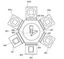
本実施の形態では、同一基板上に複数の光電変換セルを形成し、複数の光電変換セルを直列接続して光電変換装置を集積化する、集積型光電変換装置(光電変換装置モジュール)の例を説明する。また、本実施の形態では、縦方向にユニットセルが2層積層されたタンデム型光電変換装置を集積化する例を説明する。なお、図1に示すようにユニットセルを1層を有する光電変換装置を集積化してもよいし、ユニットセルを3層以上積層した光電変換装置を集積化してもよい。以下、集積型光電変換装置の作製工程および構成の概略について説明する。(Embodiment 3)
In this embodiment, an example of an integrated photoelectric conversion device (photoelectric conversion device module) in which a plurality of photoelectric conversion cells are formed over the same substrate, and the photoelectric conversion devices are integrated by connecting the plurality of photoelectric conversion cells in series. Will be explained. In this embodiment, an example in which a tandem photoelectric conversion device in which two unit cells are stacked in the vertical direction is integrated will be described. Note that as illustrated in FIG. 1, a photoelectric conversion device having one unit cell layer may be integrated, or a photoelectric conversion device in which three or more unit cells are stacked may be integrated. Hereinafter, an outline of a manufacturing process and a configuration of the integrated photoelectric conversion device will be described.
図5(A)において、基板1001上に第1電極1002を設ける。或いは第1電極1002を備えた基板1001を用意する。第1電極1002は、スパッタリング法、蒸着法、または印刷法などにより、実施の形態1の第1電極102に示す亜鉛及びアルミニウムを含む導電性酸窒化物を用いて、40nm〜200nm(好適には50nm〜100nm)の厚さで形成する。In FIG. 5A, a
第1電極1002上には、ユニットセル1010、中間導電層1003、およびユニットセル1020が順に積層形成される。ユニットセル1010およびユニットセル1020を構成する光電変換層は、ここではプラズマCVD法で作製される半導体層で構成され、pin接合に代表される半導体接合を含む。ここでは、光入射側に配置されるユニットセル1010を構成する光電変換層のi層を、ユニットセル1020の半導体層のi層よりもバンドギャップの広い半導体を用いて形成することが好ましいため、実施の形態2に示すタンデム構造を適宜用いることができる。また、中間導電層1003は、実施の形態2に示す中間導電層301と同様に形成する。On the
次に、素子分離された光電変換セルを形成し、光電変換セルを集積化する。光電変換セルの集積化方法および素子分離方法は特に限定されない。ここでは、光電変換セル毎に分離し、互いに隣接する光電変換セル同士を電気的に直列に接続する例を説明する。Next, photoelectric conversion cells separated from each other are formed, and the photoelectric conversion cells are integrated. The method for integrating the photoelectric conversion cells and the device isolation method are not particularly limited. Here, an example will be described in which photoelectric conversion cells are separated for each photoelectric conversion cell and the photoelectric conversion cells adjacent to each other are electrically connected in series.
図5(B)に示すように、同一基板上に複数の光電変換セルを形成するために、レーザ加工法によりユニットセル1010、中間導電層1003、およびユニットセル1020の積層体と第1電極1002とを貫通する開口C0〜Cnを形成する。開口C0、C2、C4、・・・Cn−2、Cnは絶縁分離用の開口であり、素子分離された複数の光電変換セルを形成するために設ける。また、開口C1、C3、C5、・・・Cn−1は、分離された第1電極と、ユニットセル1010、中間導電層1003、およびユニットセル1020の積層体上に後に形成される第2電極と、の接続を形成するために設ける。開口C0〜Cnの形成により、第1電極1002は第1電極T1〜Tmに、ユニットセル1010、中間導電層1003、およびユニットセル1020の積層体は多重接合セルK1〜Kmに分割される。なお、開口を形成するためのレーザ加工法に用いるレーザの種類は限定されるものではないが、Nd−YAGレーザやエキシマレーザなどを用いることが好ましい。いずれにしても、第1電極1002とユニットセル1010、中間導電層1003、およびユニットセル1020が積層された状態でレーザ加工を行うことにより、加工時に第1電極1002が基板1001から剥離することを防ぐことができる。As shown in FIG. 5B, in order to form a plurality of photoelectric conversion cells on the same substrate, a
図5(C)に示すように、開口C0、C2、C4、・・・Cn−2、Cnを充填し、且つ開口C0、C2、C4、・・・Cn−2、Cnの上端部を覆う絶縁層Z0〜Zmを形成する。絶縁層Z0〜Zmはスクリーン印刷法により、アクリル樹脂、フェノール樹脂、エポキシ樹脂、ポリイミド樹脂などの絶縁性のある樹脂材料を用いて形成することができる。例えば、フェノキシ樹脂にシクロヘキサン、イソホロン、高抵抗カーボンブラック、アエロジル(商標登録)、分散剤、消泡剤、およびレベリング剤を混合させた樹脂組成物を用い、スクリーン印刷法により開口C0、C2、C4、・・・Cn−2、Cnを充填するように絶縁樹脂パターンを形成する。絶縁樹脂パターンを形成した後、160℃に設定したオーブン中にて20分間熱硬化させることで、絶縁層Z0〜Zmを形成することができる。As shown in FIG. 5C, the openings C0 , C2 , C4 ,... Cn−2 , Cn are filled and the openings C0 , C2 , C4,. -2 to form an insulating layerZ 0 to Zm to cover the upper end of theC n. The insulating layers Z0 to Zm can be formed by a screen printing method using an insulating resin material such as an acrylic resin, a phenol resin, an epoxy resin, or a polyimide resin. For example, by using a resin composition in which phenoxy resin is mixed with cyclohexane, isophorone, high resistance carbon black, Aerosil (registered trademark), a dispersant, an antifoaming agent, and a leveling agent, openings C0 and C2 are formed by a screen printing method. , C4 ,... Cn-2 , Cn is formed to form an insulating resin pattern. After forming the insulating resin pattern, the insulating layers Z0 to Zm can be formed by thermosetting in an oven set at 160 ° C. for 20 minutes.
次に、図6で示す第2電極E0〜Emを形成する。第2電極E0〜Emは導電材料で形成する。第2電極E0〜Emは、アルミニウム、銀、モリブデン、チタン、クロムなどを用いた導電層をスパッタリング法や真空蒸着法で形成しても良いが、吐出形成できる導電材料を用いて形成することもできる。吐出形成できる導電材料を用いて第2電極E0〜Emを形成する場合は、スクリーン印刷法、インクジェット法、ディスペンス法などにより所定のパターンを直接形成する。例えば、Ag、Au、Cu、W、Al等の金属の導電性粒子を主成分とした導電材料を用いて、第2電極E0〜Emを形成することができる。大面積基板を用いて光電変換装置を作製する場合には、第2電極E0〜Emを低抵抗化することが好ましい。したがって、金属の粒子として抵抗率の低い金、銀、銅のいずれかの粒子、好適には低抵抗な銀或いは銅を溶媒に溶解または分散させた導電材料を用いるとよい。また、レーザ加工された開口C1、C3、C5、・・・Cn−1に導電材料を十分に充填するには、導電性粒子の平均粒径が5nm〜10nmであるナノペーストを用いることが好ましい。Next, a second electrodeE 0 to Em shown in FIG. The second electrodes E0 to Em are formed of a conductive material. The second electrode E0 to Em are aluminum, silver, molybdenum, titanium, chromium, etc. may be formed by a sputtering method or a vacuum evaporation method a conductive layer with, but is formed using a conductive material can be discharged forming You can also. When forming a second electrode E0 to Em by using a conductive material can be discharged forming a screen printing method, an inkjet method, to directly form a predetermined pattern by a dispenser method, or the like. For example, the second electrodes E0 to Em can be formed using a conductive material mainly composed of conductive particles of metal such as Ag, Au, Cu, W, and Al. When a photoelectric conversion device is manufactured using a large-area substrate, it is preferable to reduce the resistance of the second electrodes E0 to Em . Therefore, a conductive material in which any one of gold, silver, and copper having low resistivity, preferably low-resistance silver or copper is dissolved or dispersed in a solvent may be used as the metal particles. Inorder to sufficiently fill the conductive material in the laser processed openings C1 , C3 , C5 ,... Cn−1 , a nano paste having an average particle diameter of conductive particles of 5 nm to 10 nm is used. It is preferable to use it.
第2電極E0〜Emは、上記の他に、導電材料の周囲を他の導電材料で覆った導電性粒子を含む導電性組成物を吐出形成してもよい。例えば、Cuの周りをAgで覆った導電性粒子において、CuとAgの間にニッケルまたはニッケル硼素からなるバッファ層を設けた導電性粒子を用いても良い。溶媒は、酢酸ブチル等のエステル類、イソプロピルアルコール等のアルコール類、アセトン等の有機溶剤等が用いられる。吐出形成する導電性組成物の表面張力と粘度は、溶液の濃度を調整し、界面活性剤等を加えて適宜調整する。In addition to the above, the second electrodes E0 to Em may be formed by discharging a conductive composition including conductive particles in which the periphery of the conductive material is covered with another conductive material. For example, conductive particles in which the periphery of Cu is covered with Ag may be used in which a buffer layer made of nickel or nickel boron is provided between Cu and Ag. Examples of the solvent include esters such as butyl acetate, alcohols such as isopropyl alcohol, and organic solvents such as acetone. The surface tension and viscosity of the conductive composition to be discharged are adjusted as appropriate by adjusting the concentration of the solution and adding a surfactant or the like.
第2電極E0〜Emを形成する導電性組成物の吐出後は、常圧下または減圧下で、レーザビームの照射や瞬間熱アニール(RTA)、加熱炉等により、乾燥および/または焼成を行う。乾燥と焼成の工程は、両工程とも加熱処理の工程であるが、例えば、乾燥は100℃で3分間、焼成は200℃〜350℃で15分間〜120分間で行う。本工程により、導電性組成物中の溶媒を揮発する、または導電性組成物中の分散剤を化学的に除去して、周囲の樹脂を硬化収縮させることで融合と融着を加速する。乾燥と焼成を行う雰囲気は、酸素雰囲気、窒素雰囲気または大気雰囲気で行う。但し、導電性粒子を溶解または分散させている溶媒が除去されやすい酸素雰囲気下で行うことが好適である。After discharging the conductive composition forming the second electrodes E0 to Em , drying and / or baking is performed under normal pressure or reduced pressure by laser beam irradiation, rapid thermal annealing (RTA), a heating furnace, or the like. Do. The drying and baking steps are both heat treatment steps. For example, drying is performed at 100 ° C. for 3 minutes, and baking is performed at 200 ° C. to 350 ° C. for 15 minutes to 120 minutes. By this step, the solvent in the conductive composition is volatilized, or the dispersant in the conductive composition is chemically removed to cure and shrink the surrounding resin, thereby accelerating fusion and fusion. The atmosphere for drying and firing is an oxygen atmosphere, a nitrogen atmosphere, or an air atmosphere. However, it is preferable to perform in an oxygen atmosphere in which the solvent in which the conductive particles are dissolved or dispersed is easily removed.
第2電極E0〜Emは、多重接合セルK1〜Kmの最上層であるユニットセル1020と接触する。第2電極E0〜Emとユニットセル1020の接触をオーム接触とすることで接触抵抗を下げることができる。The second electrodes E0 to Em are in contact with the
第2電極E0〜Em−1のそれぞれは、開口C1、C3、C5、・・・Cn−1において、第1電極T1〜Tmのそれぞれと接続するように形成する。すなわち開口C1、C3、C5、・・・Cn−1に、第2電極E0〜Em−1と同一材料を充填する。このようにして、例えば第2電極E1は第1電極T2と電気的な接続を得て、第2電極Em−1は、第1電極Tmとの電気的な接続を得ることができる。すなわち、第2電極は、隣接する第1電極との電気的な接続を得ることができ、各多重接合セルK1〜Kmは直列に電気的な接続を得る。Each of the second electrodes E0 to Em−1 is formed so as to be connected to each of the first electrodes T1 to Tm in the openings C1 , C3 , C5 ,... Cn−1 . . That is, the openings C1 , C3 , C5 ,... Cn−1 are filled with the same material as the second electrodes E0 to Em−1 . Thus, for example, the second electrode E1 is obtained electrically connected to the first electrode T2, the second electrode Em-1, it can be electrically connected to the first electrode Tm it can. That is, the second electrode can obtain an electrical connection with the adjacent first electrode, and each of the multi-junction cells K1 to Km obtains an electrical connection in series.
以上のようにして、基板1001上に、第1電極T1と多重接合セルK1と第2電極E1からなる光電変換セルS1、・・・第1電極Tmと多重接合セルKmと第2電極Emから成る光電変換セルSmが形成される。m個の光電変換セルS1〜Smは、直列に電気的に接続されている。As described above, the photoelectric conversion cell S1 including the first electrode T1 , the multijunction cell K1 and the second electrode E1 on the
光電変換セルS1〜Sm上を覆うように、封止樹脂層1080を形成する。封止樹脂層1080は、エポキシ樹脂、アクリル樹脂、シリコーン樹脂を用いて形成すればよい。また、第2電極E0上の封止樹脂層1080に開口部1090、第2電極Em上の封止樹脂層1080に開口部1100を形成し、開口部1090、開口部1100で外部配線と接続できるようにする。第2電極E0は第1電極T1と接続されており、直列接続された光電変換セルS1〜Smの一方の取り出し電極となる。また、第2電極Emは、他方の取り出し電極となる。A sealing
本発明を適用した非単結晶半導体層を有する光電変換セルを用いて、集積型の光電変換装置を作製することができる。集積型の光電変換装置とすることで、所望の電力(電流、電圧)を得ることができる。An integrated photoelectric conversion device can be manufactured using a photoelectric conversion cell including a non-single-crystal semiconductor layer to which the present invention is applied. By using an integrated photoelectric conversion device, desired power (current, voltage) can be obtained.
なお、本実施の形態で示す構成は、本明細書の他の実施の形態で示す構成と適宜組み合わせて行うことができる。Note that the structure described in this embodiment can be combined as appropriate with any of the structures described in the other embodiments in this specification.
Claims (4)
Translated fromJapanese一導電型である第1不純物半導体層と、
半導体層と、
前記第1不純物半導体層と逆導電型である第2不純物半導体層と、が順に積層されて半導体接合を構成するユニットセルを1つ以上含み、
前記第1の電極または前記第2の電極は、亜鉛及びアルミニウムを含む導電性酸窒化物で形成されることを特徴とする光電変換装置。Between the first electrode and the second electrode,
A first impurity semiconductor layer having one conductivity type;
A semiconductor layer;
Including at least one unit cell in which the first impurity semiconductor layer and the second impurity semiconductor layer having the opposite conductivity type are sequentially stacked to form a semiconductor junction;
The first electrode or the second electrode is formed of a conductive oxynitride containing zinc and aluminum.
前記第1電極上に形成される第1のユニットセルと、
前記第1のユニットセル上に形成される中間導電層と、
前記中間導電層上に形成される第2のユニットセルと、
前記第2のユニットセル上に形成される第2の電極とを有し、
前記第1のユニットセルは、
一導電型である第1不純物半導体層と、
第1の半導体層と、
前記第1不純物半導体層と逆導電型である第2不純物半導体層と、
が順に積層されて半導体接合を構成し、
前記第2のユニットセルは、
一導電型である第3不純物半導体層と、
第2の半導体層と、
前記第3不純物半導体層と逆導電型である第4不純物半導体層と、
が順に積層されて半導体接合を構成し、
前記第1の電極、第2の電極、または中間導電層は、亜鉛及びアルミニウムを含む導電性酸窒化物で形成されることを特徴とする光電変換装置。A first electrode;
A first unit cell formed on the first electrode;
An intermediate conductive layer formed on the first unit cell;
A second unit cell formed on the intermediate conductive layer;
A second electrode formed on the second unit cell,
The first unit cell is
A first impurity semiconductor layer having one conductivity type;
A first semiconductor layer;
A second impurity semiconductor layer having a conductivity type opposite to that of the first impurity semiconductor layer;
Are stacked in order to form a semiconductor junction,
The second unit cell is
A third impurity semiconductor layer having one conductivity type;
A second semiconductor layer;
A fourth impurity semiconductor layer having a conductivity type opposite to that of the third impurity semiconductor layer;
Are stacked in order to form a semiconductor junction,
The photoelectric conversion device, wherein the first electrode, the second electrode, or the intermediate conductive layer is formed of a conductive oxynitride containing zinc and aluminum.
前記亜鉛及びアルミニウムを含む導電性酸窒化物は、
前記亜鉛の組成比が、47原子%以下であり且つ前記アルミニウムの組成比より大きく、 前記アルミニウムの組成比が窒素の組成比より大きく、
二次イオン質量分析法により測定される前記窒素の濃度が、5.0×10²⁰atoms/cm3以上である
ことを特徴とする光電変換装置。In claim 1 or 2,
The conductive oxynitride containing zinc and aluminum is
The zinc composition ratio is 47 atomic% or less and greater than the aluminum composition ratio; the aluminum composition ratio is greater than the nitrogen composition ratio;
The concentration of the said nitrogen measured by secondary ion mass spectrometry is 5.0 * 10 <20 > atoms / cm <3 > or more. The photoelectric conversion apparatus characterized by the above-mentioned.
前記亜鉛及びアルミニウムを含む導電性酸窒化物は、
前記亜鉛の組成比が47原子%以下であり、且つ前記アルミニウムの組成比より大きく、
前記アルミニウムの組成比が窒素の組成比より大きく、
1.0原子%乃至8.0原子%の前記アルミニウムを含み、且つ0.5原子%乃至4.0原子%の窒素を含む
ことを特徴とする光電変換装置。In claim 1 or 2,
The conductive oxynitride containing zinc and aluminum is
The composition ratio of the zinc is 47 atomic% or less and greater than the composition ratio of the aluminum;
The composition ratio of the aluminum is larger than the composition ratio of nitrogen,
A photoelectric conversion device comprising 1.0 atomic% to 8.0 atomic% of the aluminum and 0.5 atomic% to 4.0 atomic% of nitrogen.
Priority Applications (1)
| Application Number | Priority Date | Filing Date | Title |
|---|---|---|---|
| JP2010122394AJP2011014884A (en) | 2009-06-05 | 2010-05-28 | Photoelectric conversion device |
Applications Claiming Priority (2)
| Application Number | Priority Date | Filing Date | Title |
|---|---|---|---|
| JP2009136740 | 2009-06-05 | ||
| JP2010122394AJP2011014884A (en) | 2009-06-05 | 2010-05-28 | Photoelectric conversion device |
Related Child Applications (1)
| Application Number | Title | Priority Date | Filing Date |
|---|---|---|---|
| JP2014029257ADivisionJP5732558B2 (en) | 2009-06-05 | 2014-02-19 | Photoelectric conversion device and manufacturing method thereof |
Publications (2)
| Publication Number | Publication Date |
|---|---|
| JP2011014884Atrue JP2011014884A (en) | 2011-01-20 |
| JP2011014884A5 JP2011014884A5 (en) | 2013-05-23 |
Family
ID=43299877
Family Applications (2)
| Application Number | Title | Priority Date | Filing Date |
|---|---|---|---|
| JP2010122394AWithdrawnJP2011014884A (en) | 2009-06-05 | 2010-05-28 | Photoelectric conversion device |
| JP2014029257AExpired - Fee RelatedJP5732558B2 (en) | 2009-06-05 | 2014-02-19 | Photoelectric conversion device and manufacturing method thereof |
Family Applications After (1)
| Application Number | Title | Priority Date | Filing Date |
|---|---|---|---|
| JP2014029257AExpired - Fee RelatedJP5732558B2 (en) | 2009-06-05 | 2014-02-19 | Photoelectric conversion device and manufacturing method thereof |
Country Status (2)
| Country | Link |
|---|---|
| US (1) | US20100307590A1 (en) |
| JP (2) | JP2011014884A (en) |
Families Citing this family (4)
| Publication number | Priority date | Publication date | Assignee | Title |
|---|---|---|---|---|
| JP5489859B2 (en) | 2009-05-21 | 2014-05-14 | 株式会社半導体エネルギー研究所 | Conductive film and method for manufacturing conductive film |
| US8772627B2 (en)* | 2009-08-07 | 2014-07-08 | Semiconductor Energy Laboratory Co., Ltd. | Photoelectric conversion device and manufacturing method thereof |
| US9076909B2 (en) | 2010-06-18 | 2015-07-07 | Semiconductor Energy Laboratory Co., Ltd. | Photoelectric conversion device and method for manufacturing the same |
| WO2015029071A1 (en)* | 2013-08-30 | 2015-03-05 | Council Of Scientific And Industrial Research | Water splitting activity of layered oxides |
Citations (2)
| Publication number | Priority date | Publication date | Assignee | Title |
|---|---|---|---|---|
| WO2008134204A1 (en)* | 2007-04-27 | 2008-11-06 | Applied Materials, Inc. | Thin film semiconductor material produced through reactive sputtering of zinc target using nitrogen gases |
| JP2009099643A (en)* | 2007-10-15 | 2009-05-07 | Mitsubishi Electric Corp | Thin film solar cell element and manufacturing method thereof |
Family Cites Families (34)
| Publication number | Priority date | Publication date | Assignee | Title |
|---|---|---|---|---|
| US4387387A (en)* | 1979-08-13 | 1983-06-07 | Shunpei Yamazaki | PN Or PIN junction type semiconductor photoelectric conversion device |
| JPS57160174A (en)* | 1981-03-30 | 1982-10-02 | Hitachi Ltd | Thin film solar battery |
| JPS61222277A (en)* | 1985-03-28 | 1986-10-02 | Sanyo Electric Co Ltd | Photovoltaic device and its manufacturing method |
| US4808462A (en)* | 1987-05-22 | 1989-02-28 | Glasstech Solar, Inc. | Solar cell substrate |
| US5096505A (en)* | 1990-05-21 | 1992-03-17 | The Boeing Company | Panel for solar concentrators and tandem cell units |
| JP3035565B2 (en)* | 1991-12-27 | 2000-04-24 | 株式会社半導体エネルギー研究所 | Fabrication method of thin film solar cell |
| JP2000252500A (en)* | 1999-02-26 | 2000-09-14 | Kanegafuchi Chem Ind Co Ltd | Silicon thin-film photoelectric conversion device |
| JP4776748B2 (en)* | 1999-12-22 | 2011-09-21 | 株式会社半導体エネルギー研究所 | Solar cell |
| JP2002371357A (en)* | 2001-06-14 | 2002-12-26 | Canon Inc | Method for forming silicon-based thin film, silicon-based thin film and semiconductor element, and apparatus for forming silicon-based thin film |
| KR100416094B1 (en)* | 2001-08-28 | 2004-01-24 | 삼성에스디아이 주식회사 | Anode thin film for Lithium secondary battery and preparation method thereof |
| JP2003347572A (en)* | 2002-01-28 | 2003-12-05 | Kanegafuchi Chem Ind Co Ltd | Tandem-type thin film photoelectric conversion device and manufacturing method thereof |
| US20080090425A9 (en)* | 2002-06-12 | 2008-04-17 | Christopher Olsen | Two-step post nitridation annealing for lower EOT plasma nitrided gate dielectrics |
| US20070034251A1 (en)* | 2003-07-25 | 2007-02-15 | Ge Energy (Usa) Llc | Semiconductor elements having zones of reduced oxygen |
| US20050103377A1 (en)* | 2003-10-27 | 2005-05-19 | Goya Saneyuki | Solar cell and process for producing solar cell |
| JP4410654B2 (en)* | 2004-10-20 | 2010-02-03 | 三菱重工業株式会社 | Thin-film silicon laminated solar cell and manufacturing method thereof |
| JP2006120745A (en)* | 2004-10-20 | 2006-05-11 | Mitsubishi Heavy Ind Ltd | Thin-film silicon laminated solar cell |
| JP4454514B2 (en)* | 2005-02-14 | 2010-04-21 | 三洋電機株式会社 | Photovoltaic element, photovoltaic module including photovoltaic element, and method for manufacturing photovoltaic element |
| JP2006270021A (en)* | 2005-02-28 | 2006-10-05 | Fuji Photo Film Co Ltd | Multilayer photoelectric conversion element |
| KR20060131071A (en)* | 2005-06-15 | 2006-12-20 | 삼성전자주식회사 | Wiring for a display device, a thin film transistor array panel comprising the same, and a manufacturing method thereof |
| US8158881B2 (en)* | 2005-07-14 | 2012-04-17 | Konarka Technologies, Inc. | Tandem photovoltaic cells |
| JP2007067194A (en)* | 2005-08-31 | 2007-03-15 | Fujifilm Corp | Organic photoelectric conversion element and stacked photoelectric conversion element |
| JP2007281154A (en)* | 2006-04-06 | 2007-10-25 | Elpida Memory Inc | Manufacturing method of semiconductor device |
| US7785938B2 (en)* | 2006-04-28 | 2010-08-31 | Semiconductor Energy Laboratory Co., Ltd | Semiconductor integrated circuit, manufacturing method thereof, and semiconductor device using semiconductor integrated circuit |
| US7807917B2 (en)* | 2006-07-26 | 2010-10-05 | Translucent, Inc. | Thermoelectric and pyroelectric energy conversion devices |
| US8071872B2 (en)* | 2007-06-15 | 2011-12-06 | Translucent Inc. | Thin film semi-conductor-on-glass solar cell devices |
| US20090183774A1 (en)* | 2007-07-13 | 2009-07-23 | Translucent, Inc. | Thin Film Semiconductor-on-Sapphire Solar Cell Devices |
| US20090104462A1 (en)* | 2007-08-16 | 2009-04-23 | Reflective X-Ray Optics Llc | X-ray multilayer films and smoothing layers for x-ray optics having improved stress and roughness properties and method of making same |
| US8980066B2 (en)* | 2008-03-14 | 2015-03-17 | Applied Materials, Inc. | Thin film metal oxynitride semiconductors |
| US8022291B2 (en)* | 2008-10-15 | 2011-09-20 | Guardian Industries Corp. | Method of making front electrode of photovoltaic device having etched surface and corresponding photovoltaic device |
| JP5489859B2 (en)* | 2009-05-21 | 2014-05-14 | 株式会社半導体エネルギー研究所 | Conductive film and method for manufacturing conductive film |
| CN102460721B (en)* | 2009-06-05 | 2015-07-01 | 株式会社半导体能源研究所 | Photoelectric conversion device and method for manufacturing the same |
| KR101476817B1 (en)* | 2009-07-03 | 2014-12-26 | 가부시키가이샤 한도오따이 에네루기 켄큐쇼 | Display device including transistor and manufacturing method thereof |
| KR101066394B1 (en)* | 2009-09-02 | 2011-09-23 | 한국철강 주식회사 | Photovoltaic Device and Manufacturing Method of Photovoltaic Device |
| KR20120034964A (en)* | 2010-10-04 | 2012-04-13 | 삼성전자주식회사 | Substrate, solar cell including the substrate, and method of manufacturing the same |
- 2010
- 2010-05-28JPJP2010122394Apatent/JP2011014884A/ennot_activeWithdrawn
- 2010-06-02USUS12/792,175patent/US20100307590A1/ennot_activeAbandoned
- 2014
- 2014-02-19JPJP2014029257Apatent/JP5732558B2/ennot_activeExpired - Fee Related
Patent Citations (2)
| Publication number | Priority date | Publication date | Assignee | Title |
|---|---|---|---|---|
| WO2008134204A1 (en)* | 2007-04-27 | 2008-11-06 | Applied Materials, Inc. | Thin film semiconductor material produced through reactive sputtering of zinc target using nitrogen gases |
| JP2009099643A (en)* | 2007-10-15 | 2009-05-07 | Mitsubishi Electric Corp | Thin film solar cell element and manufacturing method thereof |
Non-Patent Citations (1)
| Title |
|---|
| JPN6013058723; K.Kobayashi: '"Electrical and optical properties of ZnO films prepared by sputtering of ZnO targets containing AlN' Applied Surface Science Vol.253, No.11, 30 March 2007, p.5035-5039* |
Also Published As
| Publication number | Publication date |
|---|---|
| JP2014140043A (en) | 2014-07-31 |
| US20100307590A1 (en) | 2010-12-09 |
| JP5732558B2 (en) | 2015-06-10 |
Similar Documents
| Publication | Publication Date | Title |
|---|---|---|
| JP5391012B2 (en) | Photoelectric conversion device | |
| US8389389B2 (en) | Semiconductor layer manufacturing method, semiconductor layer manufacturing apparatus, and semiconductor device manufactured using such method and apparatus | |
| US6287888B1 (en) | Photoelectric conversion device and process for producing photoelectric conversion device | |
| CN100472815C (en) | Electronic device and manufacturing method thereof | |
| JP4797083B2 (en) | Thin film solar cell module | |
| US8519435B2 (en) | Flexible photovoltaic cells having a polyimide material layer and method of producing same | |
| US20080153280A1 (en) | Reactive sputter deposition of a transparent conductive film | |
| US9153730B2 (en) | Solar cell front contact doping | |
| KR101747395B1 (en) | Molybdenum substrates for cigs photovoltaic devices | |
| JP5732558B2 (en) | Photoelectric conversion device and manufacturing method thereof | |
| KR101081194B1 (en) | Fabricating device of solar cell and method of fabricating using the same | |
| JP7588151B2 (en) | Manufacturing method for perovskite thin-film solar cells | |
| JP2009177224A (en) | Thin film solar cell module | |
| US20140102522A1 (en) | A-si:h absorber layer for a-si single- and multijunction thin film silicon solar cell | |
| KR101552968B1 (en) | Fabrication Method of CIGS Thin Films and its application to Thin Film Solar Cells | |
| JP2009004702A (en) | Method for manufacturing photoelectric conversion device | |
| US20130137208A1 (en) | Method for manufacturing solar cell module | |
| EP2717332A1 (en) | Method for producing solar cell | |
| JP2009177222A (en) | Thin film solar cell module | |
| US20120125406A1 (en) | Stacked photovoltaic element and method of manufacturing stacked photovoltaic element | |
| KR20150136721A (en) | Solar cell comprising high quality cigs absorber layer and method of fabricating the same | |
| KR20150136722A (en) | Solar cell comprising high quality cigs absorber layer and method of fabricating the same | |
| JP2011049304A (en) | Stacked photovoltaic element | |
| KR20100032921A (en) | Photoelectric conversion apparatus and method for manufacturing the same | |
| US20140238849A1 (en) | Methods and apparatus for controlling dopant concentration in thin films formed via sputtering deposition |
Legal Events
| Date | Code | Title | Description |
|---|---|---|---|
| A521 | Request for written amendment filed | Free format text:JAPANESE INTERMEDIATE CODE: A523 Effective date:20130402 | |
| A621 | Written request for application examination | Free format text:JAPANESE INTERMEDIATE CODE: A621 Effective date:20130402 | |
| A977 | Report on retrieval | Free format text:JAPANESE INTERMEDIATE CODE: A971007 Effective date:20131127 | |
| A131 | Notification of reasons for refusal | Free format text:JAPANESE INTERMEDIATE CODE: A131 Effective date:20131203 | |
| A521 | Request for written amendment filed | Free format text:JAPANESE INTERMEDIATE CODE: A523 Effective date:20140122 | |
| A02 | Decision of refusal | Free format text:JAPANESE INTERMEDIATE CODE: A02 Effective date:20140212 | |
| A761 | Written withdrawal of application | Free format text:JAPANESE INTERMEDIATE CODE: A761 Effective date:20140226 |