JP2011014773A - Solid-state image pick-up device and method for manufacturing the same - Google Patents
Solid-state image pick-up device and method for manufacturing the sameDownload PDFInfo
- Publication number
- JP2011014773A JP2011014773AJP2009158741AJP2009158741AJP2011014773AJP 2011014773 AJP2011014773 AJP 2011014773AJP 2009158741 AJP2009158741 AJP 2009158741AJP 2009158741 AJP2009158741 AJP 2009158741AJP 2011014773 AJP2011014773 AJP 2011014773A
- Authority
- JP
- Japan
- Prior art keywords
- pixel
- light
- color filter
- solid
- imaging device
- Prior art date
- Legal status (The legal status is an assumption and is not a legal conclusion. Google has not performed a legal analysis and makes no representation as to the accuracy of the status listed.)
- Withdrawn
Links
Images


Classifications
- H—ELECTRICITY
- H10—SEMICONDUCTOR DEVICES; ELECTRIC SOLID-STATE DEVICES NOT OTHERWISE PROVIDED FOR
- H10F—INORGANIC SEMICONDUCTOR DEVICES SENSITIVE TO INFRARED RADIATION, LIGHT, ELECTROMAGNETIC RADIATION OF SHORTER WAVELENGTH OR CORPUSCULAR RADIATION
- H10F39/00—Integrated devices, or assemblies of multiple devices, comprising at least one element covered by group H10F30/00, e.g. radiation detectors comprising photodiode arrays
- H10F39/10—Integrated devices
- H10F39/12—Image sensors
- H10F39/199—Back-illuminated image sensors
- H—ELECTRICITY
- H10—SEMICONDUCTOR DEVICES; ELECTRIC SOLID-STATE DEVICES NOT OTHERWISE PROVIDED FOR
- H10F—INORGANIC SEMICONDUCTOR DEVICES SENSITIVE TO INFRARED RADIATION, LIGHT, ELECTROMAGNETIC RADIATION OF SHORTER WAVELENGTH OR CORPUSCULAR RADIATION
- H10F39/00—Integrated devices, or assemblies of multiple devices, comprising at least one element covered by group H10F30/00, e.g. radiation detectors comprising photodiode arrays
- H10F39/80—Constructional details of image sensors
- H10F39/805—Coatings
- H10F39/8053—Colour filters
- H—ELECTRICITY
- H10—SEMICONDUCTOR DEVICES; ELECTRIC SOLID-STATE DEVICES NOT OTHERWISE PROVIDED FOR
- H10F—INORGANIC SEMICONDUCTOR DEVICES SENSITIVE TO INFRARED RADIATION, LIGHT, ELECTROMAGNETIC RADIATION OF SHORTER WAVELENGTH OR CORPUSCULAR RADIATION
- H10F39/00—Integrated devices, or assemblies of multiple devices, comprising at least one element covered by group H10F30/00, e.g. radiation detectors comprising photodiode arrays
- H10F39/80—Constructional details of image sensors
- H10F39/813—Electronic components shared by multiple pixels, e.g. one amplifier shared by two pixels
Landscapes
- Solid State Image Pick-Up Elements (AREA)
- Transforming Light Signals Into Electric Signals (AREA)
- Color Television Image Signal Generators (AREA)
Abstract
Translated fromJapaneseDescription
Translated fromJapanese本発明は、センサ部の構造に特長がある裏面照射タイプのMOS型の固体撮像装置に関する。 The present invention relates to a back-illuminated MOS solid-state imaging device having a feature in the structure of a sensor unit.
デジタルスチルカメラやカメラ付き携帯電話などの撮像デバイスとして用いられるMOS型の固体撮像装置は、複数の画素セルが二次元配置されてなるセンサ部を備えている。このセンサ部の構造について、図9および図10を用いて説明する。 A MOS type solid-state imaging device used as an imaging device such as a digital still camera or a mobile phone with a camera includes a sensor unit in which a plurality of pixel cells are two-dimensionally arranged. The structure of this sensor part will be described with reference to FIGS.
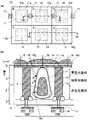
図9は従来のMOS型の固体撮像装置200の回路ブロックを示す概略構成図で、(a)は固体撮像装置200の回路ブロックを構成する画素アレイ201とその周辺の回路を示す図、(b)は画素アレイ201を構成する画素セル202の回路構成を示す図である。図10は従来の固体撮像装置200の画素部の断面図を示している(例えば、特許文献1参照)。 FIG. 9 is a schematic configuration diagram showing a circuit block of a conventional MOS type solid-
図9および図10に示すようにMOS型の固体撮像装置200において、ある特定の波長帯域の光215のみを通す数種類のカラーフィルタ204と各カラーフィルタ204の下に配置されたフォトダイオード207とを含む画素セル202が縦と横にアレイ状に配置されて画素アレイ201は構成されている(図9(a))。 As shown in FIGS. 9 and 10, in the MOS type solid-
図9(a)に示すように固体撮像装置200の回路ブロックは、上述の画素アレイ201と、画素セル202を水平方向に選択する垂直操作回路205と、画素セル202からのデータを読み出す信号線203と、画素セル202からの信号を読み出す読出し回路206とを含んで構成されている。 As shown in FIG. 9A, the circuit block of the solid-
ここで図9(b)に示すように画素セル202は、カラーフィルタ(図示せず)と、フォトダイオード207と、4つのトランジスタとを有している。この4つのトランジスタは具体的には図9(b)のような回路構成の構成要素として配置された転送トランジスタ208、増幅トランジスタ209、リセットトランジスタ210および選択トランジスタ211である。この4つのトランジスタを高速かつ安定に動作させてウェル電位を安定化させるために図9(a)に示すように画素セル202間に基板コンタクト212を配置している。 Here, as shown in FIG. 9B, the
次にこの回路構成の動作について簡単に説明する。 Next, the operation of this circuit configuration will be briefly described.
図9(b)に示すようにフォトダイオード207は、カラーフィルタを通して受光した光をその強度に応じた量の電荷に変換して蓄積する素子部であって、その一端が転送トランジスタ208のソースに接続されている。転送トランジスタ208のドレイン側は、リセットトランジスタ210のソースと増幅トランジスタ209のゲートとに接続されている。また、リセットトランジスタ210と増幅トランジスタ209のドレインは、例えば3.3Vの電位をもつ電源線に接続されており、増幅トランジスタ209のソースは選択トランジスタ211を挟んでデータを読み出すための信号線203に接続されている。なお、選択トランジスタ211は省略することも可能である。このようにして、外部からの光を画素アレイ201の中に取り込み、電気信号に変えて増幅したのち画像データとして転送している。 As shown in FIG. 9B, the
図10の従来の固体撮像装置の画素部220の断面図において、画素部220は、N型シリコン基板221の上にPウェル領域222を設け、ここにフォトダイオード207が設けられている。また、N型シリコン基板221のフォトダイオード207が形成された反対側の上層絶縁層223には、ポリシリコン転送電極(図示せず)と、その上層に銅などの材料で形成された配線層224が設けられている。また、配線層224と反対側のN型シリコン基板221上には、オンチップカラーフィルタ204およびオンチップマイクロレンズ225が設けられている。つまり、配線層224が形成されていない裏面側がフォトダイオード207の受光面となっている。これにより、開口率が大きく、また配線層224により光が反射および散乱されて跳ねられることがないため、光電感度を向上させている。 In the cross-sectional view of the
しかしながら、上記で説明した従来の技術においては、固体撮像装置の画素数が多くなるに従い、出力信号に大きなシェーディングが現われるようになるという課題が生じている。特に、可視光の中でも波長の長い、例えば赤色光のみを透過するカラーフィルタの下に配置されたフォトダイオードからの出力信号に大きなシェーディングが現われるようになるという課題が生じている。 However, in the conventional technique described above, there is a problem that a large shading appears in the output signal as the number of pixels of the solid-state imaging device increases. In particular, there is a problem that a large shading appears in an output signal from a photodiode arranged under a color filter having a long wavelength among visible light, for example, only transmitting red light.
本発明は、上記従来の課題を解決するものであって、各カラーフィルタに応じた基板コンタクトの位置によりシェーディングの発生の状態が異なるので基板コンタクトの最適配置を実施することにより、シェーディングの発生を抑制することができる固体撮像装置およびその製造方法を提供することを目的とする。 The present invention solves the above-described conventional problems, and since the state of occurrence of shading differs depending on the position of the substrate contact corresponding to each color filter, the occurrence of shading can be reduced by implementing the optimal arrangement of the substrate contacts. It is an object of the present invention to provide a solid-state imaging device that can be suppressed and a manufacturing method thereof.
上記目的を達成するために、本発明の固体撮像装置は、半導体基板の内部に形成されたフォトダイオードを含む第1の画素および第2の画素と、上記半導体基板の第1の面側であって、上記第1の画素の上部に形成された第1のカラーフィルタと、上記半導体基板の第1の面側であって、上記第2の画素の上部に形成された第2のカラーフィルタと、上記半導体基板の上記第1の面とは反対側の第2の面側に形成された積層配線層と、上記半導体基板の上記第2の面に接続された基板コンタクトと、を備え、上記第1のカラーフィルタは主に第1の光を透過し、上記第2のカラーフィルタは主に第2の光を透過し、上記第2の光の波長は上記第1の光の波長よりも短く、上記基板コンタクトは、上記第1の画素内には配置せず、上記第2の画素内に配置された構成からなる。 In order to achieve the above object, a solid-state imaging device according to the present invention includes a first pixel and a second pixel including a photodiode formed inside a semiconductor substrate, and a first surface side of the semiconductor substrate. A first color filter formed above the first pixel; a second color filter formed on the first surface side of the semiconductor substrate and above the second pixel; A laminated wiring layer formed on the second surface side opposite to the first surface of the semiconductor substrate, and a substrate contact connected to the second surface of the semiconductor substrate, The first color filter mainly transmits the first light, the second color filter mainly transmits the second light, and the wavelength of the second light is larger than the wavelength of the first light. The substrate contact is short and is not disposed in the first pixel, but the second image. Consisting placed configured within.
このような構成とすることにより、基板コンタクトの配置による空乏層の形状が変形することを防止し画素間での長波長の可視光の感度ばらつきを抑えることができるので、シェーディングの発生を抑制することができる。このことにより、画素間における長波長の可視光の感度をさらに均一にすることができる。 By adopting such a configuration, it is possible to prevent the shape of the depletion layer from being deformed due to the arrangement of the substrate contacts, and to suppress variations in sensitivity of long-wavelength visible light between pixels, thereby suppressing the occurrence of shading. be able to. As a result, the sensitivity of visible light having a long wavelength between pixels can be made more uniform.
また、半導体基板の内部に形成されたフォトダイオードを含む第3の画素をさらに備え、半導体基板の第1の面側であって、第3の画素の上部に形成された第3のカラーフィルタをさらに備え、第3のカラーフィルタは主に第3の光を透過し、第3の光の波長は第2の光の波長よりも短く、基板コンタクトは、第3の画素内にさらに配置された構成としてもよい。 In addition, a third pixel including a photodiode formed inside the semiconductor substrate is further provided, and a third color filter formed on the first surface side of the semiconductor substrate and above the third pixel is provided. In addition, the third color filter mainly transmits the third light, the wavelength of the third light is shorter than the wavelength of the second light, and the substrate contact is further disposed in the third pixel It is good also as a structure.
このような構成とすることにより、シェーディングの発生を抑制することができるだけでなく、基板コンタクトによる基板電位をさらに安定化させ画素間における感度をさらに均一にすることができる。 With such a configuration, not only the occurrence of shading can be suppressed, but also the substrate potential by the substrate contact can be further stabilized and the sensitivity between pixels can be made more uniform.
また、基板コンタクトは、第2の画素と第3の画素との境界にまたがって配置されている構成としてもよい。 In addition, the substrate contact may be arranged across the boundary between the second pixel and the third pixel.
このような構成とすることにより、基板コンタクトを画素間に配置して共有化して基板コンタクトの数を減らすことができるので画素を微細化して固体撮像装置の低コスト化および集積化を進めることができる。 With such a configuration, the number of substrate contacts can be reduced by arranging and sharing the substrate contacts between the pixels. Therefore, the cost of the solid-state imaging device can be reduced and the integration can be promoted by miniaturizing the pixels. it can.
また、基板コンタクトは、第2の画素のフォトダイオードと第3の画素のフォトダイオードとの間に形成されている構成としてもよい。 The substrate contact may be formed between the photodiode of the second pixel and the photodiode of the third pixel.
このような構成とすることにより、長波長の可視光を検出する画素から最も遠ざけることができ、画素間における長波長の可視光の感度をさらに均一にすることができる。 With such a configuration, it is possible to be farthest from a pixel that detects long-wavelength visible light, and it is possible to make the sensitivity of long-wavelength visible light between pixels more uniform.
また、基板コンタクトは、第2の画素のフォトダイオードと第3の画素のフォトダイオードとの間であって、第3の画素のフォトダイオード寄りに形成されている構成としてもよい。 Further, the substrate contact may be formed between the photodiode of the second pixel and the photodiode of the third pixel and closer to the photodiode of the third pixel.
このような構成とすることにより、基板コンタクトを最も短波長の可視光を検出する第3の画素に寄せて形成して第2の画素間で生じるわずかな感度のばらつきも抑えることができる。このことにより、画素間における感度をさらに均一にすることができる。 With such a configuration, the substrate contact is formed close to the third pixel that detects visible light having the shortest wavelength, and slight sensitivity variations occurring between the second pixels can be suppressed. As a result, the sensitivity between pixels can be made more uniform.
また、第1の光は主に赤色光であり、第2の光は主に緑色光であり、第3の光は主に青色光であり、第1の画素、第2の画素および第3の画素はベイヤー配列されている構成としてもよい。 The first light is mainly red light, the second light is mainly green light, the third light is mainly blue light, the first pixel, the second pixel, and the third light. The pixels may be arranged in a Bayer array.
このような構成とすることにより、RGBの各色に対応する光に対する感度のばらつきを抑え、シェーディングの発生をさらに抑制することができる。このことにより、画素間における感度をさらに均一にすることができる。 With such a configuration, it is possible to suppress variation in sensitivity to light corresponding to each color of RGB and further suppress the occurrence of shading. As a result, the sensitivity between pixels can be made more uniform.
また、本発明の固体撮像装置の製造方法は、半導体基板の内部に半導体基板の第1の面から入射する第1の光および第2の光を検出する、第1の画素および第2の画素を構成するフォトダイオードを形成する工程と、半導体基板の第2の面側に、第2の面に接続された基板コンタクトと積層配線層とを形成する工程と、半導体基板の第1の面側であって、第1の画素の上部に第1のカラーフィルタを形成する工程と、半導体基板の第1の面側であって、第2の画素の上部に第2のカラーフィルタを形成する工程と、を備え、第1のカラーフィルタは主に第1の光を透過し、第2のカラーフィルタは主に第2の光を透過し、第2の光の波長は第1の光の波長よりも短く、基板コンタクトは、第1の画素内には形成されず、第2の画素内に形成される方法からなる。 Further, according to the method of manufacturing the solid-state imaging device of the present invention, the first pixel and the second pixel that detect the first light and the second light that enter the semiconductor substrate from the first surface of the semiconductor substrate. Forming a photodiode constituting the semiconductor substrate; forming a substrate contact connected to the second surface and a laminated wiring layer on the second surface side of the semiconductor substrate; and a first surface side of the semiconductor substrate A step of forming a first color filter on the first pixel, and a step of forming a second color filter on the first surface side of the semiconductor substrate and on the second pixel. The first color filter mainly transmits the first light, the second color filter mainly transmits the second light, and the wavelength of the second light is the wavelength of the first light. Shorter than the substrate contact is not formed in the first pixel, but in the second pixel. Consisting of that method.
このような方法とすることにより、基板コンタクトの配置による空乏層の形状が変形することを防止し画素間での長波長の可視光の感度ばらつきを抑えることができるので、シェーディングの発生を抑制することができる。このことにより、画素間における長波長の可視光の感度をさらに均一にすることができる。 By adopting such a method, it is possible to prevent the shape of the depletion layer from being deformed due to the arrangement of the substrate contact, and to suppress the sensitivity variation of visible light having a long wavelength between pixels, thereby suppressing the occurrence of shading. be able to. As a result, the sensitivity of visible light having a long wavelength between pixels can be made more uniform.
本発明の固体撮像装置およびその製造方法によれば、基板コンタクトは長波長の可視光を検出する画素内には配置せず、短波長の可視光を検出する画素内に配置されるのでシェーディングの発生を抑制することができる。このことにより、画素間における長波長の可視光の感度をさらに均一にすることができる。 According to the solid-state imaging device and the manufacturing method thereof of the present invention, the substrate contact is not arranged in the pixel detecting the long-wavelength visible light, but is arranged in the pixel detecting the short-wavelength visible light. Occurrence can be suppressed. As a result, the sensitivity of visible light having a long wavelength between pixels can be made more uniform.
以下、本発明の実施の形態について、図面を参照しながら説明する。なお、同じ構成要素には同じ符号を付しており、説明を省略する場合もある。また、図面は、理解しやすくするためにそれぞれの構成要素を主体に模式的に示している。 Hereinafter, embodiments of the present invention will be described with reference to the drawings. In addition, the same code | symbol is attached | subjected to the same component and description may be abbreviate | omitted. Further, the drawings schematically show the respective constituent elements mainly for easy understanding.
(実施の形態1)
図1は、本発明の実施の形態1にかかる固体撮像装置の画素アレイ部10の構成を模式的に示す図で、(a)は画素アレイ部10の平面図、(b)は(a)の1B−1B線から見た断面図を示す。ただし、図1(b)の画素アレイ部10の断面図は半導体基板11の第1の面11aを上部に第2の面11bを下部にして示している。なお、本実施の形態1の固体撮像装置の画素アレイ部10以外の構成に関しては図9(a)および(b)に示した従来の構成と同様である。(Embodiment 1)
1A and 1B are diagrams schematically illustrating a configuration of a
図1(a)に示すように画素アレイ部10は、画素セルとしてRGBの3つの色の光をそれぞれ検出する第1の画素10r、第2の画素10gおよび第3の画素10bを基本的な構成として含んでいる。第1の画素10r、第2の画素10gおよび第3の画素10bは、図1(b)に示すようにフォトダイオード12、カラーフィルタ13、マイクロレンズ14および回路部(図示せず)を有している。ここで回路部は、例えば図9(b)に示すような転送トランジスタ208、増幅トランジスタ209、リセットトランジスタ210および選択トランジスタ211を含んだ回路構成からなる。 As shown in FIG. 1A, the
また、隣接するフォトダイオード12の間には、それぞれウェル電位を安定化させる基板コンタクト15が配置されており、この基板コンタクト15には基準電圧、例えば0Vが与えられている。 A
本実施の形態1に示す固体撮像装置は、図1(a)および(b)に示すように半導体基板11の内部に形成されたフォトダイオード12を含む第1の画素10rおよび第2の画素10gと、半導体基板11の第1の面11a側であって、第1の画素10rの上部に形成された第1のカラーフィルタ(図示せず)と、半導体基板11の第1の面11a側であって、第2の画素10gの上部に形成された第2のカラーフィルタ13gと、半導体基板11の第1の面11aとは反対側の第2の面11b側に形成された積層配線層16と、半導体基板11の第2の面11bに接続された基板コンタクト15と、を備えている。 The solid-state imaging device shown in the first embodiment includes a
そして第1のカラーフィルタは主に第1の光(赤色光)を透過し、第2のカラーフィルタ13gは主に第2の光(緑色光)を透過し、第2の光の波長は第1の光の波長よりも短く、基板コンタクト15は、第1の画素10r内には配置せず、第2の画素10g内に配置された構成としている。 The first color filter mainly transmits the first light (red light), the
このような構成とすることにより、後述するように基板コンタクト15の配置による空乏層17の形状が変形することを防止し第1の画素10r間での長波長の可視光の感度ばらつきを抑えることができる。したがって、シェーディングの発生を抑制することができ、第1の画素10r間における長波長の可視光の感度をさらに均一にすることができる。 By adopting such a configuration, the shape of the
以上のように構成された固体撮像装置について具体的に説明する。 The solid-state imaging device configured as described above will be specifically described.
図1(b)に示す固体撮像装置において、例えば第2の画素10gのフォトダイオード12に入射する光18はマイクロレンズ14で集光されて入射してくる。このときに第2のカラーフィルタ13gを通過しているため、波長が主に490nm以上、575nm以下の光になり、例えばシリコン材料からなる半導体基板11内の0.5μm以上、1.5μm以下の深さにおいて光電変換されてキャリアとしての電子19を発生する。ここで、フォトダイオード12の周辺に基板コンタクト15が配置されているが、光電変換は基板コンタクト15を配置することによる空乏層17の分水嶺17aがほとんど変化しない深さ約0.5μm以上、1.5μm以下で行われる。このことにより、基板コンタクト15を配置することによる感度変化の影響を受けない。 In the solid-state imaging device shown in FIG. 1B, for example, the light 18 incident on the
しかしながら、例えば第2の画素10gの上部に第2のカラーフィルタ13gが配置されずに波長が575nm以上、700nm以下の赤色光がフォトダイオード12に入射した場合には空乏層17の分水嶺17aが変化している深さが1.5μm以上、3.0μm以下のところで光電変換が行われる。このときには、光電変換されて生じた電子19aは空乏層17の分水嶺17aの変化の影響を受け、基板コンタクト15と離れる側に移動する。このことにより、赤色光がフォトダイオード12周辺に到達すると電気信号として寄与するので感度が増加することになり、感度変化を生じることになる。 However, for example, when the
また、図1(a)および(b)に示すように基板コンタクト15は、第2の画素10gのフォトダイオード12ではなく隣接する第3の画素10bのフォトダイオード12寄りに配置されている。このことにより、基板コンタクト15を配置することによる感度変化をさらに抑制できる。また、図1(b)に示すように拡散層12aを隣接するフォトダイオード12の中心を結んだ線をまたぐように配置することにより上下にレイアウト的な対象が増し、光18が入射する方向による感度変化をさらに抑制できる。 Further, as shown in FIGS. 1A and 1B, the
なお、図1(a)において第1の画素10rのフォトダイオード12に入射する光は、第2の面11bの反対側に位置する第1の面11aから入射するため、赤色光のみを透過する第1のカラーフィルタ13rを通過する。そのため、入射する光は、主に波長が575nm以上、700nm以下の光になり、半導体基板11内の深いところ(約1.5μm以上、3.0μm以下)で光電変換される。ここで、フォトダイオード12の周辺には基板コンタクト15は配置されていないため、どの方向から光が入射しても感度が変わることはない。 In FIG. 1A, light incident on the
また、同様に図1(a)の下側に配置された3つの画素10g、10r、10gのうち第1の画素10rを挟んで隣接する第2の画素10gのフォトダイオード12に入射する光は緑色光のみを透過する第2のカラーフィルタ13gを通過する。そのため、主に波長が490nm以上、575nm以下の光になり、半導体基板11内の約0.5μm以上、1.5μm以下の深さのところで光電変換される。ここで、フォトダイオード12の周辺には基板コンタクト15は配置されていないため、どの方向から光が入射しても感度が変わることはない。 Similarly, light incident on the
また、同様に図1(a)の上側に配置された3つの画素10b、10g、10bのうち第2の画素10gを挟んで隣接する第3の画素10bのフォトダイオード12に入射する光は青色光のみを透過する第3のカラーフィルタ13bを通過する。そのため、主に波長が400nm以上、490nm以下の光になり、半導体基板11内の浅いところ(約0.2μm以上、0.5μm以下)で光電変換される。このように、電荷が発生する深さが浅いため、フォトダイオード12周辺に基板コンタクト15が配置されていても空乏層17の分水嶺17aがほとんど変化しないので感度変化は生じない。 Similarly, the light incident on the
なお、光の波長に対する半導体基板11、例えばシリコン基板における吸収係数および貫通深さは図2に示すグラフのように表されることは一般的によく知られている。すなわち、図2に示す可視光およびその近傍の波長においては波長が長くなると吸収係数は小さくなり、貫通深さは大きくなる。 It is generally well known that the absorption coefficient and penetration depth in the
すなわち、本実施の形態1の固体撮像装置は、半導体基板11の内部に形成されたフォトダイオード12を含む第3の画素10bをさらに備え、半導体基板11の第1の面11a側であって、第3の画素10bの上部に形成された第3のカラーフィルタ13bをさらに備えている。この第3のカラーフィルタ13bは主に第3の光(青色光)を透過し、第3の光の波長は第2の光の波長よりも短く、基板コンタクト15は、第3の画素10b内にさらに配置された構成としている。 That is, the solid-state imaging device according to the first embodiment further includes the
このような構成とすることにより、シェーディングの発生を抑制することができるだけでなく、基板コンタクト15による基板電位をさらに安定化させ画素間における感度をさらに均一にすることができる。 With such a configuration, not only the occurrence of shading can be suppressed, but also the substrate potential by the
また、基板コンタクト15は、図1(a)および(b)に示すように第2の画素10gと第3の画素10bとの境界にまたがって配置されている構成としてもよい。 Further, as shown in FIGS. 1A and 1B, the
このような構成とすることにより、基板コンタクト15を画素間に配置して共有化して基板コンタクト15の数を減らすことができるので画素を微細化して固体撮像装置の低コスト化および集積化を進めることができる。 With such a configuration, the number of
また、基板コンタクト15は、図1(a)に示すように第2の画素10gのフォトダイオード12と第3の画素10bのフォトダイオード12との間に形成されている構成としてもよい。 Further, as shown in FIG. 1A, the
このような構成とすることにより、長波長の可視光を検出する画素、例えば第1の画素10rから最も遠ざけることができ、画素間における長波長の可視光の感度をさらに均一にすることができる。 With such a configuration, it is possible to be farthest from a pixel that detects long-wavelength visible light, for example, the
また、基板コンタクト15は、図1(a)に示すように第2の画素10gのフォトダイオード12と第3の画素10bのフォトダイオード12との間であって、第3の画素10bのフォトダイオード12寄りに形成されている構成としてもよい。 Further, as shown in FIG. 1A, the
このような構成とすることにより、基板コンタクト15を最も短波長の可視光を検出する第3の画素10bに寄せて形成して第2の画素10g間で生じるわずかな感度のばらつきも抑えることができる。このことにより、画素間における感度をさらに均一にすることができる。 By adopting such a configuration, the
また、第1の光は主に赤色光であり、第2の光は主に緑色光であり、第3の光は主に青色光であり、第1の画素10r、第2の画素10gおよび第3の画素10bはベイヤー配列されている構成としてもよい。 The first light is mainly red light, the second light is mainly green light, the third light is mainly blue light, the
このような構成とすることにより、RGBの各色に対応する光に対する感度のばらつきを抑え、シェーディングの発生をさらに抑制することができる。このことにより、画素間における感度をさらに均一にすることができる。 With such a configuration, it is possible to suppress variation in sensitivity to light corresponding to each color of RGB and further suppress the occurrence of shading. As a result, the sensitivity between pixels can be made more uniform.
以上説明したように本実施の形態1の固体撮像装置では、基板コンタクト15を第3の画素10bの第3のカラーフィルタ13bの下に配置されたフォトダイオード12の周辺に主に配置している。このような構成とすることにより、トランジスタのウェル電位を安定に固定したまま、どんな波長の光に対しても感度変化を起こすことなく、シェーディングの発生を抑えることができる。 As described above, in the solid-state imaging device according to the first embodiment, the
図3は、基板コンタクト15を隣接する画素の間に配置した固体撮像装置の画素アレイ部20の構成を模式的に示す図で、(a)は画素アレイ部20の平面図、(b)は(a)の3B−3B線から見た断面図を示す。ただし、図3(b)の画素アレイ部20の断面図は半導体基板11の第1の面11aを上部に第2の面11bを下部にして示している。なお、図3の固体撮像装置の画素アレイ部20以外の構成に関しては図9(a)および(b)に示した従来の構成と同様である。 3A and 3B are diagrams schematically illustrating a configuration of the
図1(a)の画素アレイ部10と異なり、画素アレイ部20の下側の3つの画素20g、20r、20gにおいて隣接する画素間の中央に基板コンタクト15がそれぞれ配置されている。図1(a)において基板コンタクト15は第2の画素10gより第3の画素10bの側に寄せて配置されていたが、図3(a)においては基板コンタクト15が第2の画素20gと第3の画素20bとの間のほぼ中央に配置されている。したがって、図3(b)に示すように基板コンタクト15がフォトダイオード12の位置により近いため空乏層17の分水嶺17aがさらに拡散層12aの方に張り出している。このことにより、光18が入射して深い位置で生成した電子19aに加えて中間の深さで生成した電子19の一部もフォトダイオード12周辺に到達すると電気信号として寄与するので感度が増加することになり、感度変化を生じることになる。したがって、第1の画素20r、第2の画素20gおよび第3の画素20bの間で同じ光量の光18が入射しても感度にばらつきを生じることとなる。 Unlike the
したがって、裏面照射タイプの固体撮像装置の場合、フォトダイオード12と基板コンタクト15との中間部において、赤色光を通す第1のカラーフィルタ13rを通った光18が入射された場合、半導体基板11の深い領域で光電変換により電子19aが発生する。このときに基板コンタクト15が無い場合は空乏層17の分水嶺17bは破線に示す位置となるので、電子19aはフォトダイオード12に吸収されない。しかしながら、基板コンタクト15が有る場合は空乏層17の分水嶺17aは実線に示す位置となるので、電子19aはフォトダイオード12に吸収される。これにより、フォトダイオード12の周辺に基板コンタクト15を配置するかしないかで感度に差が生じる。そのため、光18が上方向から入射される画素アレイ部20の下部では感度が下がり、光18が下方向から入射される画素アレイ部20の上部では感度が上がり、画素アレイ部20全体で見れば上部に行くほど感度が上がるシェーディングが発生する。この現象は画素セルが微細化するに伴い、基板コンタクト15による感度変化の影響の割合が大きくなるため、顕著になってくる。 Therefore, in the case of the backside illumination type solid-state imaging device, when the light 18 that has passed through the
図4は本発明の実施の形態1にかかる固体撮像装置の構成を模式的に示す図で、図1(a)の4A−4A線から見た断面図を示す。 FIG. 4 is a diagram schematically showing the configuration of the solid-state imaging device according to the first embodiment of the present invention, and shows a cross-sectional view taken along
図1(a)および図4に示すように図1(a)の下側の隣接する3つの画素10g、10r、10gには基板コンタクト15は配置されていない。したがって、光18がマイクロレンズ14を通過し第1のカラーフィルタ13rまたは第2のカラーフィルタ13gを通過して半導体基板11に入射するときに、図1(b)または図3(b)と異なり、空乏層17の分水嶺17aは半導体基板11の深いところで拡散層12aの方に膨らんでいない。このことにより、光18により生成した電子19、19aは、図4に示すようにフォトダイオード12に到達することなく拡散層12aに到達して電気信号として寄与しないので感度が増加することなく、感度変化を生じないことになる。 As shown in FIGS. 1A and 4, the
次に、以上のように構成された本実施の形態1の固体撮像装置の動作の概略について説明する。 Next, an outline of the operation of the solid-state imaging device of the first embodiment configured as described above will be described.
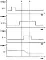
図5は本発明の実施の形態1にかかる固体撮像装置の電気的な動作を説明するタイミングチャートである。なお、以下の説明の回路構成は図9(b)に示す回路構成を想定している。 FIG. 5 is a timing chart for explaining the electrical operation of the solid-state imaging device according to the first embodiment of the present invention. Note that the circuit configuration described below assumes the circuit configuration shown in FIG.
図5に示すタイミングチャートに示すように、ある選択された1水平ライン上の画素のリセットトランジスタ210をオンするハイレベルの選択制御パルス信号φRSを与える。次いでリセットトランジスタ210をオフし、選択トランジスタ211をオンさせる制御パルス信号φSELを与える。このときの信号線sigの電位を読出し回路内にメモリする。次に転送トランジスタ208にハイレベルの選択制御パルス信号φTGを与え、フォトダイオード12から光電変換により蓄積された電荷を増幅トランジスタ209のゲート部に転送する。増幅トランジスタ209のゲート部に転送された電荷は寄生容量により電圧情報に変換され増幅トランジスタ209および選択トランジスタ211を通して信号線sigに転送される。読出し回路ではこのときの信号線sigのレベルと先にメモリした信号線sigのレベルとの差分を出力することとなる。 As shown in the timing chart shown in FIG. 5, a high-level selection control pulse signal φRS for turning on the
次に本実施の形態1の固体撮像装置の製造方法について説明する。 Next, a method for manufacturing the solid-state imaging device according to the first embodiment will be described.
図6は本発明の実施の形態1にかかる固体撮像装置の製造方法を示すフローチャートである。 FIG. 6 is a flowchart showing a method for manufacturing the solid-state imaging device according to the first embodiment of the present invention.
図6に示すように本実施の形態1の固体撮像装置の製造方法は、フォトダイオードを形成する工程と、基板コンタクト15と積層配線層16とを形成する工程と、第1のカラーフィルタ13rを形成する工程と、第2のカラーフィルタ13gを形成する工程と、を備えている。そして本実施の形態1の固体撮像装置において第1のカラーフィルタ13rは主に第1の光を透過し、第2のカラーフィルタ13gは主に第2の光を透過し、第2の光の波長は第1の光の波長よりも短く、基板コンタクト15は、第1の画素10r内には形成されず、第2の画素10g内に形成される方法としている。 As shown in FIG. 6, the manufacturing method of the solid-state imaging device according to the first embodiment includes a step of forming a photodiode, a step of forming a
ここで、フォトダイオード12を形成する工程において、半導体基板11の内部に半導体基板11の第1の面11aから入射する第1の光(主に赤色光)および第2の光(主に緑色光)を検出する、第1の画素10rおよび第2の画素10gを構成するフォトダイオード12が形成されている。また、基板コンタクト15と積層配線層16とを形成する工程において、半導体基板11の第2の面11b側に、第2の面11bに接続された基板コンタクト15と積層配線層16とが形成されている。また、第1のカラーフィルタ13rを形成する工程において、半導体基板11の第1の面11a側であって、第1の画素10rの上部に第1のカラーフィルタ13rが形成されている。同様に第2のカラーフィルタ13gを形成する工程において、半導体基板11の第1の面11a側であって、第2の画素10gの上部に第2のカラーフィルタ13gが形成されている。 Here, in the step of forming the
このような方法とすることにより、基板コンタクト15の配置による空乏層17の形状が変形することを防止し画素間での長波長の可視光の感度ばらつきを抑えることができるので、シェーディングの発生を抑制することができる。このことにより、画素間における長波長の可視光の感度をさらに均一にすることができる。 By adopting such a method, it is possible to prevent the shape of the
(実施の形態2)
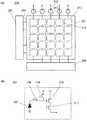
図7は、本発明の実施の形態2にかかる固体撮像装置の画素アレイ部30の構成を模式的に示す平面図である。画素アレイ部30は、図1に示す実施の形態1の画素アレイ部10とは異なり、縦に隣接して配置された2つのフォトダイオードを含んだ単位セル31、32、33がアレイ状に並べられている。このアレイ状に並べられた構成以外の構成は、画素アレイ部10と同様である。なお、図7は2つのフォトダイオードの接続がわかりやすいように接続の配線のレイヤーから見た平面図を示している。(Embodiment 2)
FIG. 7 is a plan view schematically showing the configuration of the
図8は、本発明の実施の形態2の固体撮像装置の回路ブロックを示す概略構成図で、画素アレイ部30を構成する単位セル31、32、33の回路構成を示す図である。 FIG. 8 is a schematic configuration diagram illustrating a circuit block of the solid-state imaging device according to the second embodiment of the present invention, and is a diagram illustrating a circuit configuration of the
図7および図8に示すように各単位セル31、32、33は2つの画素セルから構成される。本実施の形態2の固体撮像装置は、実施の形態1の固体撮像装置と同様に画素セルとしてRGBの3つの色の光をそれぞれ検出する第1の画素30r、第2の画素30gおよび第3の画素30bを基本的な構成として含んでいる。第1の画素30r、第2の画素30gおよび第3の画素30bは、実施の形態1と同様に図1(b)に示すフォトダイオード12、カラーフィルタ13、マイクロレンズ14および回路部(図示せず)を有している。すなわち、単位セル31は第2の画素30gおよび第3の画素30b、単位セル32は第1の画素30rおよび第2の画素30g、単位セル33は第2の画素30gおよび第3の画素30bにより構成されている。 As shown in FIGS. 7 and 8, each
回路構成は、例えば単位セル31の場合には、図8に示すように2つのフォトダイオード12と5つのトランジスタとを有している。この5つのトランジスタは、2つの転送トランジスタ208、増幅トランジスタ209、リセットトランジスタ210および選択トランジスタ211である。このうち、増幅トランジスタ209、リセットトランジスタ210および選択トランジスタ211は2つのフォトダイオード12で検出した信号の処理に共用されている。 For example, in the case of the
また、隣接するフォトダイオード12の間、すなわち上部の3つの画素30b、30g、30bの間には、それぞれウェル電位を安定化させる基板コンタクト15が配置されており、この基板コンタクト15には基準電圧、例えば0Vが与えられている。 A
以上のように構成された画素アレイ部30について説明する。 The
画素アレイ部30において転送トランジスタ208付近に基板コンタクト15を配置すると、実施の形態1と同じ原理で感度が上がり、同一の単位セル31、32、33の2つのフォトダイオード12の間で感度が異なってくる。特に転送トランジスタ208付近はそのゲートの下には転送効率を上げるためのフォトダイオード12を形成するN型の注入が入り込んでいるので、その影響を受けやすい。そのため、転送トランジスタ208と基板コンタクト15との間に別の素子、例えばリセットトランジスタ210を配置することにより2つのフォトダイオード12の感度差を抑制することができる。 When the
図7に示すような画素アレイ部30を有することにより固体撮像装置は、さらに小型化、高集積化および低コスト化をすることができる。 By having the
なお、本実施の形態2では、2画素1セルの構成を有する画素アレイ部30を一例として適用したが、本発明はこれに限定されるものではない。例えば、4画素1単位セルや6画素1単位セルなどのさらに多画素で1単位セルを構成するものを採用することもできる。 In the second embodiment, the
また、本実施の形態1および2では、画素アレイ部10、30における複数の画素10r、10g、10b、30r、30g、30bがマトリクス状に配置された構成を採用したが、本発明はこのような配置に限定されるものではない。例えば、ハニカム形状の複数の画素により画素アレイ部を構成した構造を採用してもよい。 In the first and second embodiments, a configuration in which a plurality of
また、本実施の形態1および2ではカラーフィルタとして原色フィルタを用いたが、補色フィルタやその他のカラーフィルタを組み合わせた構造を採用することもできる。 In the first and second embodiments, the primary color filter is used as the color filter, but a structure in which a complementary color filter and other color filters are combined may be employed.
また、本実施の形態1および2で説明した構成より簡単に構成して、例えばすべてのフォトダイオード間に基板コンタクトを取り、長い波長の光を通すカラーフィルタの下に配置されたフォトダイオード寄りに基板コンタクトを配置するだけでも、本発明の効果を十分に受けることができる。 In addition, the configuration is simpler than the configuration described in the first and second embodiments, and for example, substrate contacts are taken between all photodiodes, and the photodiodes are arranged near the color filters that pass light of a long wavelength. The effect of the present invention can be sufficiently received only by arranging the substrate contacts.
本発明の固体撮像装置およびその製造方法は、基板コンタクトの配置による空乏層の形状が変形することを防止して画素間での長波長の可視光の感度ばらつきを抑えることができるので、シェーディングの発生を抑制することができる。このことにより、画素間における長波長の可視光の感度をさらに均一にすることができるので、デジタルスチルカメラなどの撮像デバイスとして用いられる、高い画質性能が要求される固体撮像装置を実現することができ有用である。 Since the solid-state imaging device and the manufacturing method thereof according to the present invention can prevent the shape of the depletion layer from being deformed due to the arrangement of the substrate contacts and suppress the sensitivity variation of visible light having a long wavelength between pixels, Occurrence can be suppressed. As a result, the sensitivity of long-wavelength visible light between pixels can be made more uniform, so that a solid-state imaging device that is used as an imaging device such as a digital still camera and that requires high image quality performance can be realized. Can be useful.
10,20,30 画素アレイ部
10r,20r,30r 第1の画素
10g,20g,30g 第2の画素
10b,20b,30b 第3の画素
11 半導体基板
11a 第1の面
11b 第2の面
12 フォトダイオード
12a 拡散層
13 カラーフィルタ
13r 第1のカラーフィルタ
13g 第2のカラーフィルタ
13b 第3のカラーフィルタ
14 マイクロレンズ
15 基板コンタクト
16 積層配線層
17 空乏層
17a,17b 分水嶺
18 光
19,19a 電子
31,32,33 単位セル10, 20, 30
Claims (7)
Translated fromJapanese前記半導体基板の第1の面側であって、前記第1の画素の上部に形成された第1のカラーフィルタと、
前記半導体基板の第1の面側であって、前記第2の画素の上部に形成された第2のカラーフィルタと、
前記半導体基板の前記第1の面とは反対側の第2の面側に形成された積層配線層と、
前記半導体基板の前記第2の面に接続された基板コンタクトと、を備え、
前記第1のカラーフィルタは主に第1の光を透過し、前記第2のカラーフィルタは主に第2の光を透過し、
前記第2の光の波長は前記第1の光の波長よりも短く、
前記基板コンタクトは、前記第1の画素内には配置せず、前記第2の画素内に配置されたことを特徴とする固体撮像装置。A first pixel and a second pixel including a photodiode formed inside a semiconductor substrate;
A first color filter formed on the first surface of the semiconductor substrate and above the first pixel;
A second color filter formed on the first surface side of the semiconductor substrate and above the second pixel;
A laminated wiring layer formed on a second surface side opposite to the first surface of the semiconductor substrate;
A substrate contact connected to the second surface of the semiconductor substrate,
The first color filter mainly transmits first light, the second color filter mainly transmits second light,
The wavelength of the second light is shorter than the wavelength of the first light,
The solid-state imaging device, wherein the substrate contact is not disposed in the first pixel but is disposed in the second pixel.
前記半導体基板の前記第1の面側であって、前記第3の画素の上部に形成された第3のカラーフィルタをさらに備え、
前記第3のカラーフィルタは主に第3の光を透過し、
前記第3の光の波長は前記第2の光の波長よりも短く、
前記基板コンタクトは、前記第3の画素内にさらに配置されたことを特徴とする請求項1に記載の固体撮像装置。A third pixel including a photodiode formed in the semiconductor substrate;
A third color filter formed on the first surface of the semiconductor substrate and above the third pixel;
The third color filter mainly transmits third light,
The wavelength of the third light is shorter than the wavelength of the second light,
The solid-state imaging device according to claim 1, wherein the substrate contact is further disposed in the third pixel.
前記第1の画素、前記第2の画素および前記第3の画素はベイヤー配列されていることを特徴とする請求項2〜5のいずれか1項に記載の固体撮像装置。The first light is mainly red light, the second light is mainly green light, the third light is mainly blue light,
The solid-state imaging device according to claim 2, wherein the first pixel, the second pixel, and the third pixel are arranged in a Bayer array.
前記半導体基板の第2の面側に、前記第2の面に接続された基板コンタクトと積層配線層とを形成する工程と、
前記半導体基板の前記第1の面側であって、前記第1の画素の上部に第1のカラーフィルタを形成する工程と、
前記半導体基板の前記第1の面側であって、前記第2の画素の上部に第2のカラーフィルタを形成する工程と、を備え、
前記第1のカラーフィルタは主に前記第1の光を透過し、前記第2のカラーフィルタは主に前記第2の光を透過し、
前記第2の光の波長は前記第1の光の波長よりも短く、
前記基板コンタクトは、前記第1の画素内には形成されず、前記第2の画素内に形成されることを特徴とする固体撮像装置の製造方法。Forming a photodiode constituting the first pixel and the second pixel for detecting the first light and the second light incident from the first surface of the semiconductor substrate inside the semiconductor substrate;
Forming a substrate contact and a laminated wiring layer connected to the second surface on the second surface side of the semiconductor substrate;
Forming a first color filter on the first surface side of the semiconductor substrate and above the first pixel;
Forming a second color filter on the first surface side of the semiconductor substrate and above the second pixel, and
The first color filter mainly transmits the first light, the second color filter mainly transmits the second light,
The wavelength of the second light is shorter than the wavelength of the first light,
The method of manufacturing a solid-state imaging device, wherein the substrate contact is not formed in the first pixel but formed in the second pixel.
Priority Applications (2)
| Application Number | Priority Date | Filing Date | Title |
|---|---|---|---|
| JP2009158741AJP2011014773A (en) | 2009-07-03 | 2009-07-03 | Solid-state image pick-up device and method for manufacturing the same |
| US12/820,655US20110001207A1 (en) | 2009-07-03 | 2010-06-22 | Solid state image sensor and manufacturing method thereof |
Applications Claiming Priority (1)
| Application Number | Priority Date | Filing Date | Title |
|---|---|---|---|
| JP2009158741AJP2011014773A (en) | 2009-07-03 | 2009-07-03 | Solid-state image pick-up device and method for manufacturing the same |
Publications (1)
| Publication Number | Publication Date |
|---|---|
| JP2011014773Atrue JP2011014773A (en) | 2011-01-20 |
Family
ID=43412176
Family Applications (1)
| Application Number | Title | Priority Date | Filing Date |
|---|---|---|---|
| JP2009158741AWithdrawnJP2011014773A (en) | 2009-07-03 | 2009-07-03 | Solid-state image pick-up device and method for manufacturing the same |
Country Status (2)
| Country | Link |
|---|---|
| US (1) | US20110001207A1 (en) |
| JP (1) | JP2011014773A (en) |
Cited By (3)
| Publication number | Priority date | Publication date | Assignee | Title |
|---|---|---|---|---|
| WO2012132760A1 (en)* | 2011-03-31 | 2012-10-04 | 富士フイルム株式会社 | Solid-state imaging device and method for manufacturing solid-state imaging device |
| JP2013118345A (en)* | 2011-12-05 | 2013-06-13 | Canon Inc | Solid-state imaging apparatus, camera, and method for designing solid-state imaging apparatus |
| US9142580B2 (en) | 2012-08-10 | 2015-09-22 | Canon Kabushiki Kaisha | Image pickup apparatus and image pickup system |
Families Citing this family (5)
| Publication number | Priority date | Publication date | Assignee | Title |
|---|---|---|---|---|
| FR3011198A1 (en)* | 2013-10-02 | 2015-04-03 | St Microelectronics Sa | METHOD OF FORMING A STACK OF DIFFERENT MATERIALS AND DEVICE COMPRISING THE STACK |
| CN105810697B (en)* | 2014-12-31 | 2018-06-29 | 格科微电子(上海)有限公司 | Imaging sensor and its color recognition method |
| CN107250314B (en)* | 2015-02-27 | 2019-11-12 | 富士胶片株式会社 | Near-infrared-absorbing composition, cured film, near-infrared-absorbing filter, solid-state imaging device, and infrared sensor |
| CA2954154A1 (en) | 2016-01-11 | 2017-07-11 | Kailash C. Vasudeva | Power tool with detachable auxiliary handle |
| US11121169B2 (en)* | 2019-06-25 | 2021-09-14 | Omnivision Technologies, Inc. | Metal vertical transfer gate with high-k dielectric passivation lining |
Family Cites Families (1)
| Publication number | Priority date | Publication date | Assignee | Title |
|---|---|---|---|---|
| JP3467013B2 (en)* | 1999-12-06 | 2003-11-17 | キヤノン株式会社 | Solid-state imaging device |
- 2009
- 2009-07-03JPJP2009158741Apatent/JP2011014773A/ennot_activeWithdrawn
- 2010
- 2010-06-22USUS12/820,655patent/US20110001207A1/ennot_activeAbandoned
Cited By (6)
| Publication number | Priority date | Publication date | Assignee | Title |
|---|---|---|---|---|
| WO2012132760A1 (en)* | 2011-03-31 | 2012-10-04 | 富士フイルム株式会社 | Solid-state imaging device and method for manufacturing solid-state imaging device |
| CN103460385A (en)* | 2011-03-31 | 2013-12-18 | 富士胶片株式会社 | Solid-state imaging device and method for manufacturing solid-state imaging device |
| US8981509B2 (en) | 2011-03-31 | 2015-03-17 | Fujifilm Corporation | Solid-state imaging device and manufacturing method of solid-state imaging device |
| US9276035B2 (en) | 2011-03-31 | 2016-03-01 | Fujifilm Corporation | Solid-state imaging device and manufacturing method of solid-state imaging device |
| JP2013118345A (en)* | 2011-12-05 | 2013-06-13 | Canon Inc | Solid-state imaging apparatus, camera, and method for designing solid-state imaging apparatus |
| US9142580B2 (en) | 2012-08-10 | 2015-09-22 | Canon Kabushiki Kaisha | Image pickup apparatus and image pickup system |
Also Published As
| Publication number | Publication date |
|---|---|
| US20110001207A1 (en) | 2011-01-06 |
Similar Documents
| Publication | Publication Date | Title |
|---|---|---|
| US11282881B2 (en) | Solid-state imaging device and method of manufacturing the same, and imaging apparatus | |
| US10804328B2 (en) | Solid-state imaging device, method of manufacturing the same, and electronic apparatus | |
| KR102722463B1 (en) | Solid-state imaging device and imaging device | |
| KR100962449B1 (en) | Photoelectric conversion layer stack type color solid-state imaging device | |
| CN104637963B (en) | Solid-state imaging device, manufacturing method of solid-state imaging device, and electronic device | |
| TWI497702B (en) | Solid state camera device | |
| JP4950703B2 (en) | Solid-state image sensor | |
| JP4491323B2 (en) | Photoelectric conversion film stacked color solid-state imaging device | |
| JP2011014773A (en) | Solid-state image pick-up device and method for manufacturing the same | |
| JP4659788B2 (en) | Back-illuminated image sensor | |
| JP2011129633A (en) | Solid-state imaging device and method of manufacturing the same, and electronic apparatus | |
| JP4404561B2 (en) | MOS type color solid-state imaging device | |
| JP4388752B2 (en) | CCD color solid-state imaging device | |
| JP2006108497A (en) | Solid-state imaging device | |
| JP2008258498A (en) | Solid-state imaging device | |
| JP2010040997A (en) | Solid-state imaging element | |
| JP2013041982A (en) | Solid state image pickup device |
Legal Events
| Date | Code | Title | Description |
|---|---|---|---|
| A621 | Written request for application examination | Free format text:JAPANESE INTERMEDIATE CODE: A621 Effective date:20120404 | |
| RD02 | Notification of acceptance of power of attorney | Free format text:JAPANESE INTERMEDIATE CODE: A7422 Effective date:20120501 | |
| A761 | Written withdrawal of application | Free format text:JAPANESE INTERMEDIATE CODE: A761 Effective date:20130117 |