JP2010541468A - Compact multi-element antenna with phase shift - Google Patents
Compact multi-element antenna with phase shiftDownload PDFInfo
- Publication number
- JP2010541468A JP2010541468AJP2010527925AJP2010527925AJP2010541468AJP 2010541468 AJP2010541468 AJP 2010541468AJP 2010527925 AJP2010527925 AJP 2010527925AJP 2010527925 AJP2010527925 AJP 2010527925AJP 2010541468 AJP2010541468 AJP 2010541468A
- Authority
- JP
- Japan
- Prior art keywords
- radiating element
- antenna system
- phase shift
- antenna
- radiating
- Prior art date
- Legal status (The legal status is an assumption and is not a legal conclusion. Google has not performed a legal analysis and makes no representation as to the accuracy of the status listed.)
- Pending
Links
- 230000010363phase shiftEffects0.000titleclaimsabstractdescription112
- 239000000463materialSubstances0.000claimsabstractdescription20
- 238000004891communicationMethods0.000claimsdescription79
- 230000008878couplingEffects0.000claimsdescription2
- 238000010168coupling processMethods0.000claimsdescription2
- 238000005859coupling reactionMethods0.000claimsdescription2
- 238000012545processingMethods0.000description21
- 230000006870functionEffects0.000description20
- 230000005540biological transmissionEffects0.000description13
- 230000000694effectsEffects0.000description10
- 239000004020conductorSubstances0.000description8
- 238000000034methodMethods0.000description8
- 238000013442quality metricsMethods0.000description8
- 230000008859changeEffects0.000description6
- 238000010586diagramMethods0.000description6
- 230000005855radiationEffects0.000description6
- 230000008901benefitEffects0.000description5
- 239000011159matrix materialSubstances0.000description5
- 239000000758substrateSubstances0.000description3
- 238000013461designMethods0.000description2
- 229920000642polymerPolymers0.000description2
- 238000004904shorteningMethods0.000description2
- RYGMFSIKBFXOCR-UHFFFAOYSA-NCopperChemical compound[Cu]RYGMFSIKBFXOCR-UHFFFAOYSA-N0.000description1
- 238000003491arrayMethods0.000description1
- 230000009286beneficial effectEffects0.000description1
- 230000001143conditioned effectEffects0.000description1
- 229910052802copperInorganic materials0.000description1
- 239000010949copperSubstances0.000description1
- MPTQRFCYZCXJFQ-UHFFFAOYSA-Lcopper(II) chloride dihydrateChemical compoundO.O.[Cl-].[Cl-].[Cu+2]MPTQRFCYZCXJFQ-UHFFFAOYSA-L0.000description1
- 230000009977dual effectEffects0.000description1
- 238000005516engineering processMethods0.000description1
- 239000011888foilSubstances0.000description1
- 230000036039immunityEffects0.000description1
- 230000001788irregularEffects0.000description1
- 238000012986modificationMethods0.000description1
- 230000004048modificationEffects0.000description1
- 230000004044responseEffects0.000description1
- 239000004065semiconductorSubstances0.000description1
Images
Classifications
- H—ELECTRICITY
- H01—ELECTRIC ELEMENTS
- H01Q—ANTENNAS, i.e. RADIO AERIALS
- H01Q3/00—Arrangements for changing or varying the orientation or the shape of the directional pattern of the waves radiated from an antenna or antenna system
- H01Q3/26—Arrangements for changing or varying the orientation or the shape of the directional pattern of the waves radiated from an antenna or antenna system varying the relative phase or relative amplitude of energisation between two or more active radiating elements; varying the distribution of energy across a radiating aperture
- H—ELECTRICITY
- H01—ELECTRIC ELEMENTS
- H01Q—ANTENNAS, i.e. RADIO AERIALS
- H01Q1/00—Details of, or arrangements associated with, antennas
- H01Q1/36—Structural form of radiating elements, e.g. cone, spiral, umbrella; Particular materials used therewith
- H—ELECTRICITY
- H01—ELECTRIC ELEMENTS
- H01Q—ANTENNAS, i.e. RADIO AERIALS
- H01Q1/00—Details of, or arrangements associated with, antennas
- H01Q1/36—Structural form of radiating elements, e.g. cone, spiral, umbrella; Particular materials used therewith
- H01Q1/38—Structural form of radiating elements, e.g. cone, spiral, umbrella; Particular materials used therewith formed by a conductive layer on an insulating support
Landscapes
- Variable-Direction Aerials And Aerial Arrays (AREA)
- Details Of Aerials (AREA)
Abstract
Translated fromJapaneseDescription
Translated fromJapaneseこの発明は無線通信システム、およびそのようなシステムで使用される特に指向性アンテナに関する。 The present invention relates to wireless communication systems and particularly to directional antennas used in such systems.
無線通信システムでは、アンテナは、無線周波数信号を送受信するのに使用される。一般に、アンテナは、オムニ指向性または指向性である場合がある。多くの場合、アンテナを使用するデバイスを同封する筐体かケースの中に配置されたアンテナを有することに利益がある。しかしながら、筐体内であって、デバイスの部品の非常に近くにアンテナを配置する場合、アンテナの性能を著しく低下させうる。 In wireless communication systems, antennas are used to transmit and receive radio frequency signals. In general, an antenna may be omni-directional or directional. In many cases, it would be beneficial to have an antenna located within a housing or case that encloses a device that uses the antenna. However, if the antenna is placed within the housing and very close to the device components, the performance of the antenna can be significantly reduced.
したがって、筐体内に設置されたアンテナの性能の向上の必要がある。 Therefore, it is necessary to improve the performance of the antenna installed in the housing.
この出願は、その全体を援用する米国の仮特許出願第60/827,846の2006年10月2日の出願であって、発明の名称が「位相シフトするコンパクト多素子アンテナ」の利益を主張する。 This application is a US Provisional Patent Application No. 60 / 827,846, filed Oct. 2, 2006, which is incorporated by reference in its entirety, and claims the benefit of a “compact multi-element antenna with phase shift”. To do.
方法、装置、およびシステムは、正の利得を提供している間、上記アンテナを使用する装置の筐体内に含まれうるアンテナシステムのために説明される。一形態では、上記アンテナシステムは、アンテナビームパターンを協働して形成するアンテナ素子のアレーを含む。上記アンテナ素子は、所望のビームパターンでの上記アンテナシステムの利得を増やすために、協働する2以上の同相のアンテナ素子として配列されうる。1以上のアンテナ素子の使用は、それらのマイナス効果を上記アンテナシステムの比較的小さい部分に制限することによって上記筐体のシステムの他要素のマイナス効果を減らすことができる、全体的なアンテナシステムの長さを増加させることができる。これは、アンテナシステムのロバスト性および耐性を増加させて、アンテナがプリント回路基板アセンブリ(PCBA)かオンボードアセンブリを有する筐体に埋め込まれているのを許容する。一形態では、2以上のアンテナシステムが、選択的に同時に異なったアンテナパターンを提供するように使用される。 The method, apparatus, and system are described for an antenna system that can be included within the housing of an apparatus that uses the antenna while providing positive gain. In one form, the antenna system includes an array of antenna elements that cooperatively form an antenna beam pattern. The antenna elements can be arranged as two or more in-phase antenna elements that cooperate to increase the gain of the antenna system with a desired beam pattern. The use of one or more antenna elements can reduce the negative effects of other elements of the housing system by limiting their negative effects to a relatively small portion of the antenna system. The length can be increased. This increases the robustness and immunity of the antenna system and allows the antenna to be embedded in a housing having a printed circuit board assembly (PCBA) or on-board assembly. In one form, two or more antenna systems are used to selectively provide different antenna patterns simultaneously.
一実施形態において、フェイズドアレーアンテナシステムは、所望の周波数で共振するために選択された材料および長さからなる第1の放射素子を含む。遅延素子のような位相シフト素子は第1の放射素子の一端に結合される。第2の放射素子は第1の放射素子と反対の上記位相シフト素子の端部に結合され、無線信号は第1の放射素子を通過し、上記位相シフト素子を通過し、上記第2の放射素子を通過し、上記第2の放射素子は、上記第1および第2の放射素子が協働して上記アンテナシステムから所望のビームパターンを形成するよう、共振するために選択された材料および長さからなる。 In one embodiment, the phased array antenna system includes a first radiating element of material and length selected to resonate at a desired frequency. A phase shift element, such as a delay element, is coupled to one end of the first radiating element. A second radiating element is coupled to the end of the phase shift element opposite the first radiating element, and a radio signal passes through the first radiating element, passes through the phase shifting element, and the second radiating element. The material and length selected to resonate so that the second radiating element passes through an element such that the first and second radiating elements cooperate to form a desired beam pattern from the antenna system. It consists of.
この実施形態において、上記第1の放射素子は上記無線信号の波長の約4分の1の長さであり得るし、上記第2の放射素子は上記無線信号の波長の約2分の1の長さである。上記位相シフト素子は、上記無線信号の位相を上記無線信号の波長の約半分ほどシフトする。さらに、上記アンテナはスイッチを含み、上記スイッチの操作は、上記第1の放射素子から上記第2の放射素子を切断する。上記第1および第2の放射素子は、スイッチがオンオフされ、上記素子が共振する周波数を変更できる要素も含みうる。 In this embodiment, the first radiating element may be about a quarter of the wavelength of the radio signal, and the second radiating element is about a half of the wavelength of the radio signal. Length. The phase shift element shifts the phase of the radio signal by about half of the wavelength of the radio signal. Further, the antenna includes a switch, and operation of the switch disconnects the second radiating element from the first radiating element. The first and second radiating elements can also include elements that can change the frequency at which the switch is turned on and off and the element resonates.
他の実施形態において、フェイズドアレーアンテナシステムは、放射素子として協働するダイポール部分およびH部分を備える、下部の放射素子含む。一実施形態において、上記ダイポール部分およびH部分は、協働してダイポールアンテナとして動作する。位相シフト素子は上記下部の放射素子に結合される。端部の放射素子は、上記下部の放射素子と反対の上記位相シフト素子に結合され、上記端部の放射素子および上記下部の放射素子は、協働して所望のアンテナパターンを形成する。 In other embodiments, the phased array antenna system includes a lower radiating element comprising a dipole portion and an H portion that cooperate as radiating elements. In one embodiment, the dipole portion and H portion cooperate to operate as a dipole antenna. A phase shift element is coupled to the lower radiating element. An end radiating element is coupled to the phase shift element opposite the lower radiating element, and the end radiating element and the lower radiating element cooperate to form a desired antenna pattern.
上記アンテナシステムは、また、上記下部の放射素子と上記位相シフト素子との間のスイッチを含み、上記スイッチの操作は、上記下部の放射素子と上記位相シフト素子および上記端部の素子とを結合および分離する。上記位相シフト素子内にもまた、スイッチはあり得る。上記スイッチの操作は、上記位相シフト素子による位相シフト量を変える。 The antenna system also includes a switch between the lower radiating element and the phase shift element, and the operation of the switch couples the lower radiating element with the phase shift element and the end element. And separate. There can also be a switch in the phase shift element. The operation of the switch changes the phase shift amount by the phase shift element.
他の実施形態において、プリント配線基板、基板またはキャリアなどの回路基板は、所望の周波数で共振するために選択された材料および長さからなる第1の放射素子を含む。上記回路基板はまた、上記第1の放射素子の一端に結合された第1の位相シフト素子を含む。上記第1の放射素子と反対の上記位相シフト素子の端部に結合された第2の放射素子があり、無線信号は、第1の放射素子を通過し、上記位相シフト素子を通過し、上記第2の放射素子を通過して、上記第2の放射素子は、上記第1および上記第2の放射素子が協働して上記アンテナシステムからの所望のビームパターンを形成するよう、共振するために選択された材料および長さからなる。 In other embodiments, a circuit board, such as a printed wiring board, board or carrier, includes a first radiating element of material and length selected to resonate at a desired frequency. The circuit board also includes a first phase shift element coupled to one end of the first radiating element. There is a second radiating element coupled to the end of the phase shift element opposite the first radiating element, the radio signal passes through the first radiating element, passes through the phase shifting element, and Passing through a second radiating element, the second radiating element resonates such that the first and second radiating elements cooperate to form a desired beam pattern from the antenna system. Consisting of material and length selected.
上記回路基板はまた、上記第1の放射素子と反対の上記第2の放射素子の一端に結合された第2の位相シフト素子を含みうる。そして第3の放射素子は上記第2の放射素子と反対の第2の位相シフト素子の端部に結合される。無線信号は第1の放射素子を通過し、上記第1の位相シフト素子を通過し、第2の放射素子を通過し、上記第2の位相シフト素子を通過し、そして第3の放射素子を通過して、上記第3の放射素子は、上記第1、第2および第3の放射素子が協働して上記アンテナシステムからの所望のビームパターンを形成するように、共振するために選択された材料および長さからなる。他の実施形態において、どのような所望の数の放射素子および位相シフト素子も、アンテナシステムにおいて用いられうる。 The circuit board may also include a second phase shift element coupled to one end of the second radiating element opposite the first radiating element. The third radiating element is coupled to the end of the second phase shift element opposite to the second radiating element. A wireless signal passes through the first radiating element, passes through the first phase shifting element, passes through the second radiating element, passes through the second phase shifting element, and passes through the third radiating element. In passing, the third radiating element is selected to resonate such that the first, second and third radiating elements cooperate to form a desired beam pattern from the antenna system. Material and length. In other embodiments, any desired number of radiating elements and phase shifting elements can be used in the antenna system.
さらに他の実施形態において、回路基板は第1のアンテナシステムがある第1の面および第2のアンテナシステムがある第2の面を含む。上記2つのアンテナシステムは異なる周波数で作動する。例えば、カードの第1の側面には、第1の所望の周波数で共振するために選択された材料および長さからなる第1の放射素子と、上記第1の放射素子の一端と結合される第1の位相シフト素子と、上記第1の放射素子と反対の上記位相シフト素子の端部に結合される第2の放射素子があり、その結果、無線信号は第1の放射素子を通過し、位相シフト素子を通過し、第2の放射素子を通過して、上記アンテナシステムからの所望のビームパターンを形成するために、上記第1および上記第2の放射素子が協働するように、上記第2の放射素子は、共振するために選択された材料および長さからなる。上記カードの第2の側面には、第2の所望の周波数で共振するために選択された材料および長さからなる第3の放射素子と、上記第3の放射素子の一端に結合された第2の位相シフト素子と、上記第1の放射素子と反対の上記第2の位相シフト素子の端部に結合された第4の放射素子とを備える第2のアンテナシステムがある。その結果、無線信号は第1の放射素子を通過し、位相シフト素子を通過し、第2の放射素子を通過して、上記アンテナシステムからの所望のビームパターンを形成するために、上記第1および上記第2の放射素子が協働するように、上記第2の放射素子は共振するために選択された材料および長さからなる。 In yet another embodiment, the circuit board includes a first surface with a first antenna system and a second surface with a second antenna system. The two antenna systems operate at different frequencies. For example, the first side of the card is coupled to a first radiating element of material and length selected to resonate at a first desired frequency and one end of the first radiating element. There is a first radiating element and a second radiating element coupled to the end of the phase shifting element opposite the first radiating element, so that the radio signal passes through the first radiating element. The first and second radiating elements cooperate to form a desired beam pattern from the antenna system, passing through the phase shifting element and passing through the second radiating element, The second radiating element comprises a material and a length selected to resonate. The second side of the card includes a third radiating element of material and length selected to resonate at a second desired frequency, and a first radiating element coupled to one end of the third radiating element. There is a second antenna system comprising two phase shift elements and a fourth radiating element coupled to the end of the second phase shifting element opposite the first radiating element. As a result, the radio signal passes through the first radiating element, through the phase shifting element, and through the second radiating element to form the desired beam pattern from the antenna system. And the second radiating element comprises a material and a length selected to resonate so that the second radiating element cooperates.
他の実施形態において、図12および図13で図示された回路基板のようなキャリアは、フレキシブルで、堅く、平面、または曲線でありうる。上記キャリアはある形に成形されるか、筐体への付属などの拘束による形のままでありうる。他の実施形態において、アンテナシステムはキャリアの複数のセクションの向こう側にわたりうる。どんな所望の角度でもキャリアのセクションを互いに並べられうる。 In other embodiments, a carrier such as the circuit board illustrated in FIGS. 12 and 13 can be flexible, rigid, planar, or curved. The carrier may be molded into a certain shape or remain in a shape due to constraints such as attachment to a housing. In other embodiments, the antenna system can span across multiple sections of the carrier. The sections of the carrier can be aligned with each other at any desired angle.
上述のアンテナは、無線通信デバイスで使用されうる。一実施形態において、無線通信デバイスは筐体を含む。上記デバイスはまた、電子部品およびグランドプレーンを有するプリント回路基板を含む。第1の放射素子、位相シフト素子および第2の放射素子を含む少なくとも1つのフェイズドアレーアンテナシステムがある。上記第1および第2の放射素子は上記位相シフト素子の反対の端部に結合され、上記第1および第2の放射素子は、所望の周波数における無線信号が上記第1の素子に、そして上記位相シフト素子を通過し、上記第2の放射素子に送られるときに、協働して所望のビームパターンを形成する。 The antenna described above can be used in a wireless communication device. In one embodiment, the wireless communication device includes a housing. The device also includes a printed circuit board having electronic components and a ground plane. There is at least one phased array antenna system that includes a first radiating element, a phase shifting element, and a second radiating element. The first and second radiating elements are coupled to opposite ends of the phase shift element, and the first and second radiating elements are configured to transmit a radio signal at a desired frequency to the first element and to the As it passes through the phase shift element and is sent to the second radiating element, it cooperates to form the desired beam pattern.
一実施形態において、上記無線通信デバイスは多数のビームパターンが形成されるような上記デバイスにおいて指向される多数のフェイズドアレーアンテナシステムを含む。上記アンテナシステムを含みうる無線通信デバイスの実例には、無線ルータ、モバイルアクセスポイント、あるいは他のタイプの無線デバイスが含まれる。 In one embodiment, the wireless communication device includes multiple phased array antenna systems that are directed at the device such that multiple beam patterns are formed. Examples of wireless communication devices that can include the antenna system include wireless routers, mobile access points, or other types of wireless devices.
一実施形態において、無線通信デバイスは筐体、無線機、そして上記筐体内に位置する少なくとも2つのフェイズドアレーアンテナシステムを含み、上記アンテナシステムは、第1の放射素子と、位相シフト素子と、第2の放射素子とを備え、上記第1および第2の放射素子は上記位相シフト素子の反対と端部に結合され、上記第1および第2の放射素子は、所望の周波数における無線周波数信号が上記少なくとも1つのフェイズドアンテナシステムに送られるときに、協働して所望のビームパターンを形成する。上記デバイスはまた、上記無線機を上記少なくとも二つのアンテナシステムに結合するスイッチと、上記少なくとも二つのアンテナシステムのうちの1つを上記無線機に選択的に結合するために上記スイッチを制御する制御器も含む。一実施形態において、無線信号が上記第1の放射素子を通過し、上記位相シフト素子を通過して、上記第2の放射素子に送られる。一実施形態において、上記第1の放射素子は、放射素子として協働するダイポール部分およびH部分を備える下部の放射素子であり、上記第2の放射素子は端部の放射素子であり、無線信号は、上記位相シフト素子に結合される上記下部の放射素子の端部に送られる。 In one embodiment, a wireless communication device includes a housing, a radio, and at least two phased array antenna systems located within the housing, the antenna system including a first radiating element, a phase shift element, a first Two radiating elements, wherein the first and second radiating elements are coupled to opposite ends of the phase shift element, the first and second radiating elements receiving radio frequency signals at a desired frequency. When sent to the at least one phased antenna system, it cooperates to form a desired beam pattern. The device also includes a switch that couples the radio to the at least two antenna systems and a control that controls the switch to selectively couple one of the at least two antenna systems to the radio. Including a bowl. In one embodiment, a wireless signal passes through the first radiating element, passes through the phase shift element, and is sent to the second radiating element. In one embodiment, the first radiating element is a lower radiating element comprising a dipole portion and an H portion that cooperate as a radiating element, the second radiating element is an end radiating element, and a radio signal Is sent to the end of the lower radiating element coupled to the phase shift element.
さらに他の実施形態において、無線通信デバイスは、筐体、少なくとも二つの無線機、上記筐体内に位置する少なくとも二つのフェイズドアレーアンテナシステムを含み、上記アンテナシステムは、第1の放射素子、位相シフト素子および第2の放射素子を備え、上記第1および第2の放射素子は、上記位相シフト素子の反対の端部に結合され、上記第1および第2の放射素子は、所望の周波数における無線周波数信号が上記少なくとも1つのフェイズドアンテナシステムに送られるときに、協働して所望のビームパターンを形成する。上記デバイスは、各無線機に結合される1つのアンテナを有し、様々な無線機から各アンテナへの適切な信号を送るための基礎的な処理を行う電気回路を使用しうる。例えばいくつかの無線機は、他の無線機が起動している間、スイッチが切られ、あるいは上記デバイスは、上記無線信号の異なる位相シフトおよび大きさを活用し、そのパフォーマンスを最大化するために上記指向性アンテナを用いる。上記デバイスはまた、上記少なくとも二つの無線機を上記少なくとも二つのアンテナシステムに結合するスイッチマトリクスと、上記無線機の1つを上記アンテナシステムの1つに選択的に結合するために上記スイッチマトリクスを制御する制御器と、異なるアンテナシステムへの異なる無線機とを含みうる。一実施形態において、無線信号が上記第1の放射素子を通過し、上記位相シフト素子を通過して、上記第2の放射素子に送られる。他の実施形態において、上記第1の放射素子は、放射素子として協働するダイポール部分およびH部分を備える、下部の放射素子であり、上記第2の放射素子は、端部の放射素子であり、無線信号は、上記位相シフト素子に結合される上記下部の放射素子の端部に送られる。他の実施形態において、上記埋め込まれたアンテナは、上記位相シフト機能を使っているのではなく、むしろ、上記所要の指向性パターンを形成するために上記筐体内の他の要素からの反射を活用している。 In yet another embodiment, a wireless communication device includes a housing, at least two radios, and at least two phased array antenna systems located within the housing, the antenna system comprising a first radiating element, a phase shift. An element and a second radiating element, wherein the first and second radiating elements are coupled to opposite ends of the phase shift element, the first and second radiating elements being wireless at a desired frequency. When a frequency signal is sent to the at least one phased antenna system, it cooperates to form a desired beam pattern. The device may have an antenna coupled to each radio and use an electrical circuit that performs the basic processing to send the appropriate signals from the various radios to each antenna. For example, some radios are switched off while other radios are activated, or the device takes advantage of different phase shifts and magnitudes of the radio signal to maximize its performance. The above directional antenna is used. The device also includes a switch matrix that couples the at least two radios to the at least two antenna systems, and the switch matrix to selectively couple one of the radios to one of the antenna systems. It may include a controller to control and different radios to different antenna systems. In one embodiment, a wireless signal passes through the first radiating element, passes through the phase shift element, and is sent to the second radiating element. In another embodiment, the first radiating element is a lower radiating element comprising a dipole portion and an H portion that cooperate as radiating elements, and the second radiating element is an end radiating element. The radio signal is sent to the end of the lower radiating element coupled to the phase shift element. In another embodiment, the embedded antenna does not use the phase shift function, but rather utilizes reflections from other elements in the housing to form the required directional pattern. is doing.
この発明の他の特徴および利点は、以下の詳細な説明および添付の図面を概観した後に、当業者にとって、より容易に明白になるだろう。 Other features and advantages of the present invention will become more readily apparent to those skilled in the art after reviewing the following detailed description and accompanying drawings.
これらおよび他の形態、この発明の利点および詳細は、その構造および操作の双方に関して、同様の参照番号が同様の部分を参照する添付図面の調査によって、一部収集されうる。上記図面は必ずしも実寸図示したものではなく、この発明の原理を図解するのに重点が置かれている。
ここで開示されるような、ある実施形態は、広帯域の無線インタフェース(broadband wireless air interface)に関する通信のための方法、デバイスおよびシステムを提供する。この説明を読んだ後に、様々な代替可能な実施形態および適用例においてこの発明の実施の方法が明白になるだろう。しかしながら、ここでこの発明の様々な実施形態が説明されるが、これらの実施形態が制限ではなく実施例のみとして示されることが理解される。そのようなものとして、様々な代替可能な実施形態についてのこの詳細な説明は、添付された請求項で示されるような、この発明の範囲や幅を制限するために解釈されるべきでない。 Certain embodiments, as disclosed herein, provide methods, devices, and systems for communication over a broadband wireless air interface. After reading this description, the manner of carrying out the invention will become apparent in various alternative embodiments and applications. However, while various embodiments of the invention will now be described, it is understood that these embodiments are shown by way of example only and not limitation. As such, this detailed description of various alternative embodiments should not be construed to limit the scope or breadth of the present invention as set forth in the appended claims.
一実施形態において、アンテナは、無線周波数信号を送受信するためにアンテナを用いるデバイスの筐体内に含められうる。上記アンテナは、所望の方向、あるいはパターンに放射し、かつ、オムニ指向性アンテナと比較して、送信された信号の方向やパターンにおいて正の利得を与えるように構成されうる。一形態において、アンテナは、所望のビームパターンを協働して形成するアンテナ素子の配置を含む。上記アンテナ素子の配置および上記素子に与える信号の位相関係は、ビームパターンを形成するために用いられ得る。また、デバイスの筐体内の上記アンテナ素子の位置および、上記デバイス内の他の電子部品に対するアンテナ素子の配置は、所望のビームパターンを形成するのに用いられうる。例えば、上記デバイスの上記筐体がプラスチックで作られている場合、上記筐体は、アンテナ素子の配置や位相整合を決定するときに考慮されうる上記アンテナシステムに「塑性負荷」を与えうる。さらに、上記デバイスにおいて、他の電子部品およびプリント回路基板(PCB)の配置は、上記アンテナに負荷を与え、アンテナ素子の配置や位相整合を決定するときに考慮されうる。一実施形態において、筐体に封入されたアンテナは、上記筐体内の他の構成要素に作用し、そして相互作用する場合に、所望のビームパターンを形成するように構成されている。 In one embodiment, the antenna may be included in the housing of a device that uses the antenna to transmit and receive radio frequency signals. The antenna can be configured to radiate in a desired direction or pattern and provide a positive gain in the direction and pattern of the transmitted signal compared to an omni-directional antenna. In one form, the antenna includes an arrangement of antenna elements that cooperatively form a desired beam pattern. The arrangement of the antenna elements and the phase relationship of signals applied to the elements can be used to form a beam pattern. Further, the position of the antenna element in the housing of the device and the arrangement of the antenna element with respect to other electronic components in the device can be used to form a desired beam pattern. For example, if the housing of the device is made of plastic, the housing can provide a “plastic load” to the antenna system that can be considered when determining antenna element placement and phase matching. Further, in the device, the arrangement of other electronic components and a printed circuit board (PCB) can be taken into account when applying a load to the antenna and determining the arrangement and phase matching of the antenna elements. In one embodiment, an antenna encapsulated in a housing is configured to form a desired beam pattern when acting on and interacting with other components within the housing.
一実施形態において、上記アンテナは、それらが所望のビームパターンにおける上記アンテナシステムの利得を協働して増加させるように、配置されうるアンテナ素子を含む。2以上のアンテナ素子を用いることで、上記アンテナシステムの比較的より小さい部分に他の構成要素の負の効果を制限することにより、上記筐体の上記システムの他の構成要素の負の効果を減少できる上記アンテナシステムの全長を増加させられる。一形態において、上記2以上のアンテナは、異なるアンテナのパターンを同時にあるいは選択的に提供するために用いられる。 In one embodiment, the antennas include antenna elements that can be arranged such that they cooperatively increase the gain of the antenna system in a desired beam pattern. By using two or more antenna elements, the negative effects of the other components of the system of the enclosure are limited by limiting the negative effects of the other components to a relatively smaller portion of the antenna system. The total length of the antenna system that can be reduced can be increased. In one form, the two or more antennas are used to provide different antenna patterns simultaneously or selectively.
以下の説明において、多くの長さおよび距離が、上記アンテナに用いられる無線周波数の波長の点から表現される。例えば、上述のアンテナシステムは、およそ2.0ギガヘルツ(GHz)、5.0Ghz、あるいは他の選択された周波数のような、いかなる所望の周波数(あるいは周波数に集中したバンド)における操作のため構成されうる。当然のことながら、波長(λ)が用いられる場合、それは、無線周波数が通過する材料の誘電体の効果(λd)が通常考慮されることになっている。このように、以下の議論において特に言及しない限り、波長は、上記無線周波数が通過する材料の誘電体の効果(λd)が考慮される。In the following description, many lengths and distances are expressed in terms of the wavelength of the radio frequency used for the antenna. For example, the antenna system described above is configured for operation at any desired frequency (or band concentrated in frequency), such as approximately 2.0 gigahertz (GHz), 5.0 Ghz, or other selected frequencies. sell. Of course, when wavelength (λ) is used, it is usually taken into account the dielectric effect (λd ) of the material through which the radio frequency passes. Thus, unless specifically mentioned in the following discussion, the wavelength takes into account the dielectric effect (λd ) of the material through which the radio frequency passes.
一実施形態において、アンテナは、アンテナ素子および配列のような位相関係で配列される位相シフト素子を含む。アンテナ素子および位相シフト素子は、所望の方向、パターンのアンテナの放射されたビームパターンを導くように協働する。また、上記アンテナは、回路カード、筐体内のプリント回路基板(PCB)組立、上記筐体内の主要構成要素、しばしば筐体の塑性負荷とみなされる上記筐体自体に関連した上記アンテナの位置を考慮するように、アンテナ素子および位相シフト素子も配列されうる。 In one embodiment, the antenna includes phase shift elements arranged in a phase relationship such as antenna elements and arrays. The antenna element and the phase shift element cooperate to direct the radiated beam pattern of the antenna in the desired direction, pattern. The antenna also takes into account the position of the antenna relative to the circuit card, the printed circuit board (PCB) assembly in the housing, the main components in the housing, and the housing itself, which is often regarded as a plastic load on the housing. As such, antenna elements and phase shift elements may also be arranged.
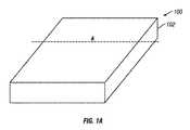
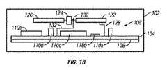
図1は、無線通信デバイス100の斜視図を含む。上記通信デバイス100は外ケースまたは筐体102を含む。図1Bは、図1Aに図示された無線通信デバイスについての断面図である。図1Bで示されるように、多層回路でありうるプリント回路基板(あるいは他の適当なキャリア)104がケースで囲まれる。プリント回路基板はまたグランドプレーン106を含みうる。通信デバイス内に含まれた回路素子、半導体チップ、電源および他の構成要素は、プリント回路基板104に配置された構成要素110a〜eとして一般に表わされる。一実施形態において、上記通信デバイスは、プリント回路基板104に配置された無線機を含む無線ネットワークカードの構成要素を含む。代わりに、上記通信デバイスは、無線ルータ、モバイルのアクセスポイントあるいは他のタイプの無線通信デバイスになりえる。 FIG. 1 includes a perspective view of a
一実施形態において、上記デバイス100におけるアンテナシステム108は、パッシブフェイズドアレーである。パッシブフェイズドアレーは、あるいはアンテナ素子122、例えば、位相反転器または遅延素子を含むかもしれない位相シフト素子、124、また第2の放射、あるいはアンテナ素子126を含む。上記通信デバイスの上記無線機は、接続部128を介して無線信号を送受信する第1のアンテナ素子に連結される。一実施形態において、接続部128は同軸ケーブルおよび適切なコネクターである。あるいは、接続部128は上記プリント回路基板104への第1のアンテナ素子122の端に接続されたピン(図示せず)の接合によりなすことができる。 In one embodiment, the
一実施形態において、第1および第2のアンテナ素子122および126は、選択された周波数で所望の放射を達成するために、それらの電気的な長さを選択する導体になりえる。例えば、導体は回路基板あるいは他の適当なキャリア上でのトレースになりえる。別の実施例において、導体は、プリント基板や基板またはキャリアのような回路基板に付けられた、あるいは貼り付けられる配線の長さ、あるいは上記筐体の壁になりえる。上記導体の長さは例えば、作動頻度、導電材の誘電性の値、導体の波形率などに基づいて選択することができる。 In one embodiment, the first and
一実施形態において、上記位相シフト素子124は位相や遅れ、信号を180度ずつ変える。上記位相シフト素子によって、上記二つのアンテナ素子122と126は、所望のアンテナ放射あるいはビームまたはパターンを生成するアンテナシステム108全体に付加的な利得効果を有する。他の実施形態において、上記2つのアンテナ素子間の所望の連結を得るために、上記位相シフト素子124は、いずれかの所望量によって第2のアンテナ素子126に送る信号の位相をシフトしてもよい。 In one embodiment, the
一実施形態において、ピンダイオードのようなスイッチ130は、第1のアンテナ素子122と位相シフト素子124の間に配置される。制御線はスイッチ130を制御するために用いられうる132である。スイッチが閉の場合、アンテナシステム108は上述の方法で作動する。スイッチが開の場合、第1のアンテナ素子122だけが使用可能である。このように、スイッチは、アンテナ100が2つの異なったパターンを持つことを可能にする。 In one embodiment, a
さらに、第1のアンテナ素子122および/または第2のアンテナ素子126は、構成要素(図示せず)のスイッチがオンあるいはオフの場合、上記アンテナ素子の共振周波数を変更することができる、切り替えられた上記構成要素を含むかもしれない。上記切り替えられた構成要素は、それらの共振周波数を変更することができるように上記アンテナ素子を設定可能にする能力を与える。上記アンテナ素子の共振周波数の変更は、上記素子を電気的に延長するか短くすることと見なされるかもしれない。このように、上記アンテナ素子の各々は、関連する切り替えられた構成要素の状態に依存して、異なった周波数で共振するために構成されうる。一実施形態において、1つの切り替えられた構成要素だけが、上記アンテナ素子のうちのただ一つだけが用いられる。上記切り替えられた構成要素は、制御線、あるいは信号経路に加えられたバイアス電圧で制御されうる。 Further, the
一実施形態において、第1のアンテナ素子122、第2のアンテナ素子126および位相シフト素子124は、すべて設定可能になりえる。例えば、上述したように、上記アンテナ素子は設定可能になりえる。上記位相シフト素子は、例えば、電気的にショートした位相シフト素子の部分が位相シフト素子124の全長あるいは遅れを有効に減少させる、切り替えられた構成要素を含めることにより構成されうる。このように、上記アンテナおよび位相シフト素子は、異なった放射パターンを協働して作成するように、異なった方法で構成されうる。他の実施形態において、位相シフト素子は、上記位相シフト素子によってもたらされた位相シフトを変更するためにその全長を増加する場合がある。さらに、上記アンテナおよび位相シフト素子は、異なる周波数において作動し、あるいは共振するために構成されうる。 In one embodiment, the
一実施形態において、上記アンテナ素子は上記通信デバイス110a〜eの構成要素の上に配置され、プリント回路基板の面と平行に一般に配置される。この方向は、例えば、上記プリント回路基板上の同じアンテナシステムに関連したそれらの構成要素の離調効果を減少させることができる。 In one embodiment, the antenna element is disposed on components of the communication devices 110a-e and is generally disposed parallel to the plane of the printed circuit board. This orientation can, for example, reduce the detuning effects of those components associated with the same antenna system on the printed circuit board.
一実施形態において、上記アンテナシステムがより多くの指向性アンテナパターンを生成するために、プリント回路基板104のグランド層106は反射器として働くことができる。反射量は、上記アンテナシステムとグランド層との間の距離によって影響を受ける。例えば、伝送経路において伝送された信号のおよそ4分の1の波長(λd/4)の範囲内の距離は、充分な反射を与えるだろう。In one embodiment, the
上記筐体100はアンテナシステム108への負荷として働くだろう。例えば、上記筐体の壁、上面および底面に関連した上記アンテナ素子の位置は、上記アンテナシステム108によって生成されたビームパターンを修正できる。上記筐体の壁厚、上記筐体の構造で用いられる材料などの筐体の特徴は、所望の放射パターンを生成するための上記アンテナ素子の設計および配置において考慮されうる。 The
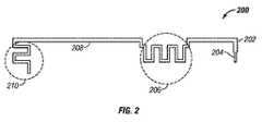
図2は、図1Aに図示された通信デバイスのようなデバイス内で用いられうるアンテナ200の実施形態の平面図である。上記アンテナ200は、タブ204から位相シフト素子206に及ぶ、第1のアンテナ素子202を含む。一実施形態において、タブ204は、例えば、アンテナに無線機を接続するストリップラインに、またはそれを経由して、プリント回路基板あるいは他のキャリアにはんだ付けされうる。一実施形態において、第1のアンテナ素子202の寸法は、伝送経路において伝送された信号のおよそ2分の1の波長(λd/2)である。この実施形態において、上記位相シフト素子206は、上記伝送経路において伝送された信号の2分の1の波長(λd/2)の遅延線として構成される。FIG. 2 is a plan view of an embodiment of an
図2の実施例において、第2のアンテナ素子208は、位相シフト素子206の出力に連結される。上記第2のアンテナ素子208の反対側の端部は、伝送経路において伝送された信号のおよそ4分の1の波長(λd/4)の反射距離である、第2の位相シフト素子、すなわち遅延線210に連結される。上記反射距離は、上記アンテナが用いられる周波数範囲、上記伝送経路の誘電率および上記アンテナの所望の効率を考慮に入れて選択されうる。一実施形態において、第2のアンテナ素子208の反対側の位相シフト210の端部は、上記アンテナ200のための接地接続にはんだづけされる。この実施形態において、上記アンテナは、機械的なサポートおよび信号の接続をするための、プリント回路基板への2つの接続点を有する。In the embodiment of FIG. 2, the
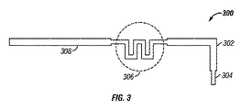
図3は、図1Aに図示された通信デバイスのようなデバイス内で用いられうるアンテナ300の他の実施形態の平面図である。上記アンテナ300は、図2のアンテナ200と同様に、第1のタブ304から延在する、第1のアンテナ素子302を含む。第1のアンテナ素子302の反対側の端部は位相シフト素子306に連結される。位相シフト素子の反対側の端部は第2のアンテナ素子308に連結される。この実施形態において、第2のアンテナ素子308の反対側の端部は電気的に開であり、未結合である。 FIG. 3 is a plan view of another embodiment of an
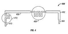
図4は、図1Aに図示された通信デバイスのようなデバイス内で用いられうるアンテナ400の他の実施形態の平面図である。上記アンテナ400は図2のアンテナ200と同様であり、第1のタブ404から延在する、第1のアンテナ素子402を含む。第1のアンテナ素子402の反対側の端部は、位相シフト素子406に連結される。位相シフト素子の反対側の端部は、第2の位相シフト素子410にその反対側の端部を接続する、第2のアンテナ素子408に連結される。第2の位相シフト線410は第2のタブ412に連結される。図4のアンテナ400は図2のアンテナ200とは異なった周波数で動作するように構成される。例えば、第1および第2のアンテナ素子402および404は、異なった材料で構築するか、あるいは異なった波形率を有する。図4の実施例において、位相シフト素子408および410は、異なった材料で構築されるか、異なった波形率を有することにより、異なった周波数で所望の位相シフトを提供できる。例えば、図4の第1および第2の位相シフト素子406および410の全長は、図2の位相シフト素子206および210の全長よりも短いかもしれない。 FIG. 4 is a plan view of another embodiment of an
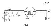
図5は、図1Aに図示された通信デバイスのようなデバイス内で用いられうるアンテナ500の他の実施形態の平面図である。上記アンテナ500は図4のアンテナ400と同様であり、第1のアンテナ素子402、第1のタブ404、位相シフト素子406、第2のアンテナ素子408、第2の位相シフト素子410および第2のタブ412を含む。アンテナ500は、また第2のアンテナ素子408に連結された負荷502を含む。上記負荷502は、第2のアンテナ素子の共振周波数およびアンテナ整合を変更するために選択されうる。 FIG. 5 is a plan view of another embodiment of an
図5は第2のアンテナ素子408に連結された負荷502の実施例を図示しているが、他の実施形態において、負荷は、上記アンテナ500における他の素子に連結されうる。さらに、負荷はアンテナ500において2以上の素子に連結されうる。また、アンテナ素子に連結されたり、外れたり、切り替えられうるように、上記負荷は構成されうる。 Although FIG. 5 illustrates an example of a
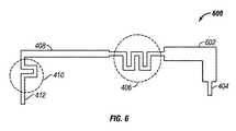
図6は、図1Aに図示された通信デバイスのようなデバイス内で用いられうるアンテナ600の他の実施形態の平面図である。図6に示されたアンテナ600は、図4のアンテナ400と同様であり、第1のアンテナ素子602、第1のタブ404、位相シフト素子406、第2のアンテナ素子408、第2の位相シフト素子410および第2のタブ412を含む。図600の実施例において、上記第1のアンテナ素子602には、図4の第1のアンテナ素子402とは異なる波形率がある。図6の第1のアンテナ素子602の異なった波形率は、図4において第1のアンテナ素子402の共振周波数からの第1のアンテナ素子602の共振周波数を変更できる。 FIG. 6 is a plan view of another embodiment of an
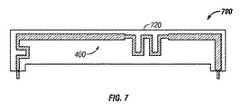
図7は、図1Aに図示された通信デバイスのようなデバイス内で用いられうるアンテナ700の実施形態の平面図である。図7に示された実施例において、上記アンテナシステム700は、ポリマーまたはプラスチック成型720に入れられた、図4に示されるようなアンテナ400を含む。通常、ケーシングはアンテナの誘電率を変更する。例えば、ポリマーまたはプラスチックのケーシングは、通常より小さな(より短い)アンテナ素子を同様に考慮するλdを通常減少させる。上記アンテナの導体素子は、型押しされた銅片あるいは基板上でパターンのある伝導性のフォイルとして、低費用で製造される。あるいは、上記ケーシングは、鋳型に注入された鋳型および導体材料を含むかもしれない。上記アンテナ上の上記ケーシングは、全面的なデバイスの組立を大いに単純化することができる真空ピックアンドプレース機による使用に適している平面を含むかもしれない。この実施形態がRFコネクターあるいは同軸ケーブルを必要としないことが注目される。上記アンテナは、回路基板アセンブリーと容易に結合する、別個の、あらかじめ調整されたアセンブリーになりえる。他の実施形態において、アンテナの異なった形態はすっぽりと包まれうる。FIG. 7 is a plan view of an embodiment of an
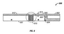
図8は、図1Aに図示された通信デバイスのようなデバイス内で用いられうるアンテナ800の実施形態の平面図である。図8に図示された上記アンテナは、プリント回路基板あるいは他の適当なキャリア、あるいはバッキングの小片上で銅トレースとして形成されうる。図8に示された実施形態において、上記アンテナシステム800は、接地接続804を含むH部分802を含む。上部のダイポール部分806は、無線機に上部のダイポール部分806を連結する伝送経路接続808を含む。上部のダイポール部分806およびH部分802は総体として下部の放射素子とされ、放射素子として協働する。一実施形態において、上部のダイポール部分806およびH部分802は、ダイポールアンテナのように作用するように協働する。上部のダイポール部分806は位相シフト素子810に連結される。一実施形態において、位相シフト素子810は上記伝送経路において伝送された信号のおよそ2分の1の波長(λd/2)の遅延線である。位相シフト素子810の反対側の端部は端部の放射素子812に連結される。上記端部の放射素子812および下部の放射素子は、所望のアンテナパターンを形成するためにアンテナシステム800全体に付加的な利得効果を有する。H部分802は、またアンテナ整合およびチューニングのため、さらなる特徴を提供する。FIG. 8 is a plan view of an embodiment of an
一実施形態において、ピンダイオードのようなスイッチ814は、下部の放射素子と位相シフト素子810の間に配置される。他の実施形態において、スイッチ814は位相シフト素子810に沿って所望の場所に配置される。制御線(示されない)はスイッチ814を制御するために用いられうる。スイッチ814が閉の場合、アンテナシステム800は上述の方法で作動する。スイッチ814が開の場合、下部の放射素子だけが機能する。このように、スイッチ814は、アンテナシステム800が二つの異なった放射、ビーム、パターンを有することができる。 In one embodiment, a
さらに、より低い放射素子および/または端部の放射素子812は、構成要素(図示せず)のスイッチがオンあるいはオフの場合、上記アンテナ素子の共振周波数を変更することができる、切り替えられた上記構成要素を含むかもしれない。上記切り替えられた構成要素は、それらの共振周波数を変更することができるように上記アンテナ素子を設定可能にする能力を与える。上記アンテナ素子の共振周波数の変更は、上記素子を電気的に延長するか短くすることと見なされるかもしれない。このように、上記アンテナ素子の各々は、関連する切り替えられた構成要素の状態に依存して、異なった周波数で共振するために構成されうる。一実施形態において、1つの切り替えられた構成要素だけが、上記アンテナ素子のうちのただ一つだけが用いられる。上記切り替えられた構成要素は、制御線、あるいは信号経路に加えられたバイアス電圧で制御されうる。 Further, the lower radiating element and / or the
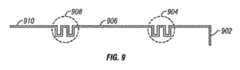
図9は、図1Aに図示された通信デバイスのようなデバイス内で用いられうるアンテナ900の他の実施形態の平面図である。図9に図示された上記アンテナシステムは、多数のアンテナ素子からなるアンテナシステムの一例を図示する。図9に示されるように、アンテナシステム900は第1のアンテナ素子902、第1の位相シフト素子904、第2のアンテナ素子906、第2の位相シフト素子908および第3のアンテナ素子910を含む。図9の実施例は3つのアンテナ素子および二つの位相シフト素子を示しているが、どんな所望の数のアンテナ素子および位相シフト素子でもアンテナシステムの中で用いることができる。一実施形態において、第1のアンテナ素子902の寸法はおよそ4分の1の波長(λd/4)である。そして、位相シフト素子および他のアンテナ素子は、伝送経路において伝送された信号のおよそ2分の1の波長(λd/2)である。他の実施形態において、素子は波長の他の分数になりえる。FIG. 9 is a plan view of another embodiment of an antenna 900 that may be used in a device such as the communication device illustrated in FIG. 1A. The antenna system illustrated in FIG. 9 illustrates an example of an antenna system including a plurality of antenna elements. As shown in FIG. 9, the antenna system 900 includes a
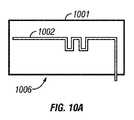
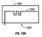
図10Aは、回路基板か基板のようなキャリア1001の第1の側面の平面図である。図10Aに示されるように、キャリアまたは回路基板1001の第1の側面1006は、第1の周波数で作動するように構成されうる第1のアンテナ1002を含む。図10Bは、図10Aで図示されたキャリア1001の第2の側面の平面図である。図10Bに示されるように、キャリア1001の第2の側面1008は、第2の周波数で作動するように構成されうる第2のアンテナ1004を含む。このように、図10AおよびBに図示された上記アンテナシステムは、2重のバンドアンテナとして2つの異なった周波数で作動できる。他の実施形態において、追加のアンテナシステムは、多重バンドアンテナを有するためにキャリア1001に含まれうる。他の実施形態において、第1および第2のアンテナは同じ周波数で作動するように構成されうる。アンテナ1002および1004は、図2〜9に図示された実施例のうちのどれに従っても実装されうる。 FIG. 10A is a plan view of a first side of a
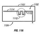
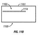
図11Aは、アンテナシステムの一部を含むキャリアの第1の側面の平面図である。図11Aに示されるように、キャリアまたは回路基板の1101の第1の側面1104は、第1のアンテナ素子1110、位相シフト素子1112および第2のアンテナ素子1114の一部のような、アンテナ1102の一部を含み得る。図11Bは、図11Bは、アンテナシステムの他の部分を含む図11Aに図示されたキャリアの、第2の側面の平面図である。図11Bに示されるように、第2のアンテナ素子1114は、同じPCB上を経由した、あるいは製造された、キャリアまたは回路基板の1101の第2の側面まで及ぶ。他の実施形態において、アンテナは、キャリアか回路基板の第2の側面上のキャリアまたは回路基板1101の端部まわりに続く。アンテナ素子がキャリアの第2の側面まで及ぶ効果は、第1のアンテナ素子、第2のアンテナ素子、あるいは位相シフト素子の長さに沿って、いかなる場所にも位置されうる。一実施形態において、2以上の要素が、所望の周波数で共振する、異なったバンドあるいは多重バンドにある場合がある。アンテナ1102は、図2〜9に図示された実施例のうちのどれに従っても実装されうる。 FIG. 11A is a plan view of the first side of the carrier including a portion of the antenna system. As shown in FIG. 11A, the
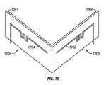
図12はアンテナシステムの他の実施形態の斜視図である。図12に示されるように、キャリア、または回路基板は、2つの部分1200および1201を含む。2つの部分はお互いに角度をなしうる。例えば、それらはお互いに直交し、あるいは60度、45度、あるいは所望の角度にある場合がある。一実施形態において、キャリア部1200および1201は各々アンテナシステム1202および1204を含む。他の実施形態において、キャリア部1200および1201上のどんな所望の数のアンテナシステムもあり得る。また、各部のアンテナシステムの数は異なってもよい。一実施形態において、2つのキャリア部1200および1201は付けられる2つの別個の部分である。他の実施形態において、2つのキャリア部は単一ユニットである。アンテナ1202および1204は、図2〜9に図示された実施例のうちのどれに従っても実装されうる。 FIG. 12 is a perspective view of another embodiment of the antenna system. As shown in FIG. 12, the carrier or circuit board includes two
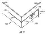
図13はアンテナシステムの他の実施形態の斜視図である。図13において、図12の実施形態と同様に、キャリア、または回路基板は、2つの部分1300および1301を含む。2つの部分はお互いに角度をなしうる。例えば、それらはお互いに直交し、あるいは60度、45度、あるいは所望の角度にある場合がある。一実施形態において、キャリア部1300および1301は各々、少なくともアンテナシステム1302の一部を含む。例えば、図13の実施例において、第1の部分1300は第1の放射素子1310、位相シフト素子1312および第2の放射素子1314の一部を含む。第2の放射素子1314はキャリアの第2の部分1301上に延在する。他の実施形態において、キャリアの第2の部分1301上に延在するアンテナ1302の部分は、アンテナ1302のいずれかの部分になりえる。また、他の実施形態において、キャリア部1300および1301上のどんな所望の数のアンテナシステムもあり得る。また、各部のアンテナシステムの数は異なってもよい。一実施形態において、2つのキャリア部1300および1301は付けられる2つの別個の部分である。他の実施形態において、2つのキャリア部は単一ユニットである。アンテナ1302は、図2〜9に図示された実施例のうちのどれに従っても実装されうる。 FIG. 13 is a perspective view of another embodiment of the antenna system. In FIG. 13, similar to the embodiment of FIG. 12, the carrier or circuit board includes two
他の実施形態において、図12および13に示されたキャリアのようなキャリアは、フレキシブル、固い、平面、曲面でもよい。キャリアは型をとられるか、あるいは筐体の付属物のような拘束によって、形状が保持されうる。他の実施形態において、アンテナはキャリアの複数の部分を横切って測ることができる。キャリアの部分は、いかなる所望の角度でも互いに整列されうる。 In other embodiments, a carrier such as that shown in FIGS. 12 and 13 may be flexible, rigid, flat, curved. The carrier can be shaped or held in shape by constraints such as enclosure accessories. In other embodiments, the antenna can be measured across multiple portions of the carrier. The portions of the carrier can be aligned with each other at any desired angle.
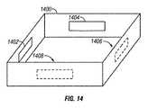
他の実施形態において、2以上のアンテナシステムはダイバーシティシステムの中で用いられうる。図14は、複数のアンテナシステムを含む無線通信デバイスの筐体1400の斜視図である。図14で例示されるように、デバイス1400は略長方形である。他の実施形態において、上記筐体は、楕円形、円形、あるいは他の不揃いな形状のような、他の形状になりえる。 In other embodiments, two or more antenna systems can be used in a diversity system. FIG. 14 is a perspective view of a
図14に示された実施例において、筐体1400は4つのアンテナシステム1402、1404、1406および1408を含む。各アンテナシステム1402、1404、1406および1408は、筐体1400の側壁のうちの1つに沿って整列される。アンテナシステムは図2〜13に図示された実施例のうちのどれに従っても実装されうる。一実施形態において、各アンテナシステムはそれぞれ一般に外へ、そしてアンテナシステムに対して垂直に延在するビームパターンを生成するように構成される。 In the embodiment shown in FIG. 14, the
図14の実施例は、4つのアンテナシステム1402、1404、1406および1408を含むが、他の実施形態において、異なる数のアンテナシステムが用いられうる。例えば、筐体は、1、2、3、4、それ以上のアンテナシステムを使用しうる。同様に、アンテナシステムの異なる指向性が、所望のビームパターンを生成するのに使用されうる。 The example of FIG. 14 includes four
ここで説明されているアンテナシステムは、様々な無線通信プロトコル及び様々な周波数範囲において用いられうる。例えば、上記システムは、周波数領域で、約2ギガヘルツ及び5ギガヘルツを中心としたバンドを有して、用いられうる。 The antenna system described herein can be used in different wireless communication protocols and different frequency ranges. For example, the system can be used with a band centered around 2 GHz and 5 GHz in the frequency domain.
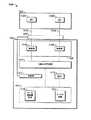
ここで説明されている実施形態は、さまざまな無線システムに結合し、用いられる上述のシステムの組み合わせである。図15は図2〜13に示されたアンテナのような多くのアンテナを用いる無線通信デバイス1500の実施形態の機能ブロック図である。無線デバイス1500は、例えば、無線ルータ、モバイルアクセスポイント、無線ネットワークアダプタ、あるいは他のタイプの無線通信デバイスがあり得る。さらに、無線デバイスはMIMO(多入出力)(multiple−in multiple−out)技術を用いることができる。無線デバイス1500は無線システム1504と通信する2つのアンテナシステム1502aおよび1502bとを含む。他の実施形態において、アンテナ1502とは異なる数が使用されるかもしれない。図15に示された例では、各アンテナは、予定されたパターンで放射するために構成される。他の実施形態において、異なるパターンで放射するために制御可能にアンテナは構成される。 The embodiments described herein are a combination of the systems described above that are used and coupled to various wireless systems. FIG. 15 is a functional block diagram of an embodiment of a
無線システム1504は無線サブシステム1522を含む。図15の実施例において、無線サブシステム1522は、2つの無線機1510aおよび1510bを含む。他の構成において、無線機1510の異なる数が含まれる。無線機1510aおよび1510bはMIMO信号処理モジュール、あるいは信号処理モジュール1512と通信する。無線機1510aおよび1510bは、アンテナ1502aおよび1502bによって送信される無線信号を生成し、アンテナの1502aおよび1502bからの無線信号を受け取る。一実施形態では、スイッチマトリクス、またはスイッチの多数である1506が、選択されたアンテナシステム1502aおよび1502bを無線機に結合するために、ライン1508aおよび1508bを送受信するために選択的に無線機1510aおよび1510bを結合する。制御器1507は、選択的に所望のアンテナシステム1502aおよび1502bに、ライン1508aおよび1508bを結合するために、スイッチマトリクス1506の操作を制御できる。他の実施形態において、各アンテナ1502aおよび1502bは単一の対応する無線機1510aおよび1510bに結合される。各無線機が送受信ライン1508aおよび1508bの送受信によって対応するアンテナと通信するとして図示されているが、より多くのラインが用いられうる。
信号処理モジュール1512は、MIMO処理を実装する。MIMO処理は、当業者によく知られ、またアンテナ1502aおよび1502bを使用している2以上の無線チャネルに情報を送って、複数の無線チャネルおよびアンテナを介して情報を受け取るための処理を含む。信号処理モジュールは、多重アンテナを通してただ一つのデータストリームの中に受け取られた情報を結合できる。信号処理モジュールは、無線システムのメディアアクセス制御(media access control)(MAC)機能のいくつか、またはすべてを実装し、MIMOシステムとして機能するように無線機の操作を制御するかもしれない。一般に、MAC機能は、通信デバイスとの送受信に1以上の物理チャネルにおける利用可能帯域幅を割り当てるために作動する。MAC機能は、優先事項による様々なサービスとそれらのサービスの質によって課されたルールの間の利用可能帯域幅を割り当てることができる。さらに、MAC機能は、TCP/IPのような上位層と、物理チャネルのような物理的な層との間の送信データを送信するために作動する。ここに図の特定の機能ブロックまで説明された機能のつながりは記述の容易さのためだけのものである。様々な機能をブロックの中で動かして、ブロックを超えて共有されて、様々に分類される。 The
中央演算処理デバイス(CPU)1514は上記信号処理モジュール1512と通信する。上記CPU1514は信号処理モジュール1512とMAC機能のいくつかを共有しうる。さらに、上記CPUはデータ通信量制御モジュール1516を含み得る。データ通信量コントロールは、例えば、DSL接続、そして、または、TCP/IPルーティングのようなデータ通信量に関連したルーティングを含み得る。信号処理モジュール1512とCPU1514の両方によってアクセスされうる共通または共有のメモリ1518を使用できる。これはCPUと信号処理モジュールの間のデータパケットの効率の良い輸送を考慮する。 A central processing unit (CPU) 1514 communicates with the
一実施形態において、上記CPU1514は、上記アンテナ1502aおよび1502bの上記図示しないスイッチモジュールを制御できる。例えば、CPU1514は、アンテナ1502aおよび1502bでスイッチを構成するために制御信号を提供できる。あるいはまた、CPU1514は、アンテナ1502aおよび1502bの図示しない制御器に、上記スイッチモジュールの所望の構成を示す信号を提供でき、そして、アンテナの制御器は上記スイッチモジュールを制御できる。他の実施形態では、スイッチモジュールを制御するための制御信号が無線信号に結合されうる。 In one embodiment, the
一実施形態において、コミュニケーションリンクに関する各送信および/または受信信号の信号品質メトリック(signal quality metric)は、アンテナのどのビームパターン方向が好まれるか、例えばRF信号を発信あるいは受信するのが望まれるのはどの方向かを決定するのにモニターされうる。信号品質メトリックは上記MIMO信号処理モジュール1512から提供されうる。MIMO信号処理モジュールは、無線通信デバイス1500と無線通信デバイスが交信する予定であるステーションとの間のコミュニケーションリンクの信号品質メトリックをする前に、MIMO処理を考慮に入れる能力を有する。例えば、各コミュニケーションリンクのために、上記信号処理モジュールは受信ダイバーシチ、最大比合成、および空間多重方式の各MIMO技術から選択できる。また、異なった無線機に接続された異なったアンテナのアンテナパターンが指向性であるという事実を利用する間、送信か受信のどちらか、あるいはその両方のダイバーシチを用いて、このように効果的にどの無線機を動かしたら良いかを選択する技術も使用できる。例えば、データスループットまたはエラー率のような信号処理モジュールから受信した信号品質メトリックは、用いられているMIMO技術に基づいて変えられる。受信した信号強度のような信号品質メトリックも、1つ以上の無線機1510aおよび1510bから供給されうる。上記信号品質メトリックは、どのアンテナ、および使用するのが望ましい上記アンテナのビームパターンの方向を決定または選択するのに用いられうる。例えば、上記信号品質メトリックは、アンテナ1502aおよび1502bのスイッチモジュールの所望の構成を決定するのに用いられうる。 In one embodiment, the signal quality metric of each transmitted and / or received signal for the communication link is preferred for which beam pattern direction of the antenna is preferred, eg, to transmit or receive an RF signal. Can be monitored to determine which direction. A signal quality metric may be provided from the MIMO
他の実施形態では、上記無線通信デバイス1500はスイッチマトリクス1506を含まない。この実施形態では、各無線機1510aおよび1510bは、送受信線1508aおよび1508bによって、それぞれアンテナ1502aおよび1502bに結合される。この構成では、信号処理モジュール1512、CPU1512、または他のモジュールは、デバイス1500の操作の間に1つのラジオか他のラジオを選ぶことができる。 In other embodiments, the
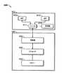
図16は、図2〜13に表現されるように、1以上のアンテナでありうるアンテナシステム1612を使用するかもしれない無線通信デバイス1600の他の実施形態の機能ブロック図である。無線デバイス1600は、例えば、無線ルータ、モバイルアクセスポイント、適合された無線ネットワーク、あるいは他のタイプの無線通信デバイスでもよい。図16の実施形態では、上記通信デバイス1600は、無線システム1604と通信するアンテナシステム1602を含む。図14の例では、無線システム1604は無線モジュール1606、プロセッサモジュール1608、およびメモリーモジュール1610を含む。上記無線モジュール1606はプロセッサモジュール1608と通信する。上記無線モジュール1606は、上記アンテナシステム1602によって送信され、上記アンテナシステムからの無線信号を受信する無線信号を生成する。 FIG. 16 is a functional block diagram of another embodiment of a
上記プロセッサモジュール1608は、上記無線システム1604用のメディアアクセス制御(MAC)機能のいくつか又はすべてを実装し、無線モジュール1606の上記操作を制御しうる。一般に、MAC機能は、通信デバイス1400へおよび通信デバイス1400からの送信について1以上の物理チャネルの利用可能帯域幅を割り当てるために作動する。MAC機能は優先度に基づく様々なサービスとそれらのQoSによって課されたルールとの間の利用可能帯域幅を割り当てることができる。さらにMAC機能は、TCP/IPのような上位層と、物理チャネルのような物理層との間でデータを移動するために作動できる。ここに図の特定の機能ブロックに説明された機能の関連性は、記述の容易さのためだけのものである。様々な機能がブロック間で動かされ、ブロック間で共有され、様々に分類されうる。上記プロセッサはまた、操作中の一時的保存と同様に、上記デバイス1600操作中に上記プロセッサモジュール1608によって実行されるコードを保存できる上記メモリーモジュール1610と通信する。 The
図16の例では、上記アンテナ1602はセンサ/スイッチモジュール1614およびコントロールモジュール1616を含む。一実施形態において、上記センサ/スイッチモジュールは、アンテナ1612aおよび1612bへ、上記無線機モジュール1604へ、および上記無線機モジュール1604から、信号を通信するために、アンテナ1612aおよび1612bと、上記無線機モジュール1604と通信する。上記センサ/スイッチモジュール1614は、所望の構成でビームパターンを形成するために上記アンテナ1612aおよび1612bを選択する、そして/または、構成する、上記アンテナシステム1602のスイッチモジュールを制御するために操作できる。また、上記センサ/スイッチモジュール1614は、上記制御器1616に信号品質の表示を与えることができ、上記制御器1616は、信号品質の表示に基づく所望の構成でアンテナの1612aおよび1612bを選択する、そして/または、構成するために上記センサ/スイッチモジュール1614を制御できる。例えば、スイッチ/センサは伝達信号の反射率を測定できる。上記アンテナは、それぞれの構成において、所望の構成を選択するために比較される、各構成に関連した信号品質表示で設定される。 In the example of FIG. 16, the
図16の説明が、上記アンテナシステム1602に位置している上記センサ/スイッチ1614について説明する一方で、上記センサ/スイッチは例えば上記無線システムの他の位置でありうる。さらに、上記センサ/スイッチ1614によって実行された機能は、全システムの他のモジュールで実行されうる。 While the description of FIG. 16 describes the sensor /
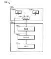
図17は上述の図2〜13に表現されるように、1つ以上のアンテナでありうるアンテナシステムを含む無線通信デバイス1700のさらに別の実施形態の機能ブロック図である。無線デバイス1700は、例えば、無線ルータ、モバイルアクセスポイント、適合された無線ネットワーク、あるいは他のタイプの無線通信デバイスでもよい。図17の実施形態では、通信デバイス1700は無線システム1704と通信するアンテナシステム1702を含む。図17の例では、無線システム1704は無線モジュール1706、プロセッサモジュール1708、およびメモリーモジュール1710を含む。上記無線モジュール1706はプロセッサモジュール1708と通信する。上記無線モジュール1706は、上記アンテナシステム1702によって送信され、上記アンテナシステムからの無線信号を受信する無線信号を生成する。 FIG. 17 is a functional block diagram of yet another embodiment of a
図17の例では、上記アンテナ1702は所望の方向に放射するために構成されうる。上記アンテナが放射する方向は、上記センサ/スイッチモジュール1714によって制御されうる。センサ/スイッチモジュール1714の操作は、受信した信号強度などのような、信号品質メトリックに対する応答において、上記アンテナシステム1712から信号を放射するための所望の方向を選択できる。一実施形態において、上記信号メトリックは上記無線機1706から上記プロセッサモジュール1708へ通信されうるし、上記プロセッサモジュール1706は所望の方向を選択するためにセンサ/スイッチモジュール1714を操作する。他の実施形態では、上記センサ/スイッチモジュール1714は、信号メトリックの表示を上記プロセッサモジュール1708に伝え、そして、上記プロセッサモジュールは所望の構成で上記アンテナを構成するために、センサ/スイッチモジュール1714を操作する。 In the example of FIG. 17, the
図17の説明が、上記アンテナシステム1702に位置している上記センサ/スイッチモジュール1714について説明する一方で、上記センサ/スイッチは、例えば上記無線システムの他の位置でありうる。さらに、上記センサ/スイッチ1714によって実行された機能は、全システムの他のモジュールで実行されうる。 While the description of FIG. 17 describes the sensor /
他の実施形態では、ここで説明される上記アンテナシステムは、最適化された指向性アンテナシステムという題がつけられた、2005年8月22日出願の米国特許出願第11/209,358で説明されたシステムと、それを参照することによって組み込まれて、結合されうる。例えば、上記出願の図6に表現されたシステムでは、要素602として上述のアンテナシステムが用いられうる。同じことが図7の要素703a〜nおよび図8の要素602にも当てはまる。また他の実施形態では、ここで説明される上記アンテナシステムは、最適化された指向性のMIMOアンテナシステムという題がつけられた、2006年12月19日仮出願の米国特許出願第60/870,818で説明されたシステムと、それを参照することによって組み込まれて、結合されうる。例えば、そのケースの図6に表現されたシステムでは、上述されたアンテナシステムが要素602として使用されうる。同じことが、図7の要素703a〜n、図8Aおよび8bの要素802a〜d、および図10の要素602にも当てはまる。 In another embodiment, the antenna system described herein is described in US patent application Ser. No. 11 / 209,358, filed Aug. 22, 2005, entitled Optimized Directional Antenna System. And can be incorporated and combined with the referenced system. For example, in the system represented in FIG. 6 of the above application, the antenna system described above can be used as
上記アンテナの様々な特性は、波長や頻度などのパラメータに関する一例として、ここに実施形態で説明される。当然のことながら、提供された例が、所望の特性を示すように電気的に現れる局面を説明する。 Various characteristics of the antenna will be described in the embodiment as an example regarding parameters such as wavelength and frequency. It will be appreciated that the aspect in which the provided example appears electrically to exhibit the desired characteristics.
開示された実施形態の上述の説明は、当業者が上記発明を作るあるいは用いることができるように提供される。これらの実施形態の多くの変更は、容易に当業者に明らかであろう、そして、この発明の趣旨あるいは範囲から逸脱せずに、ここに定義された原理は他の実施形態に適用されうる。したがって、この発明は、ここに示された実施形態に制限されることを意図しないが、上記原則および開示された新規な特徴と一致した最も広い範囲と一致させられる。 The above description of the disclosed embodiments is provided to enable any person skilled in the art to make or use the above-described invention. Many modifications of these embodiments will be readily apparent to those skilled in the art, and the principles defined herein may be applied to other embodiments without departing from the spirit or scope of the invention. Accordingly, the present invention is not intended to be limited to the embodiments shown herein but is to be accorded the widest scope consistent with the above principles and the disclosed novel features.
ここで開示された実施形態と関連して説明された、上記様々な実例となる論理ブロック、モジュール、および回路は、一般用途のプロセッサ、ディジタル信号処理(DSP)、特定用途向IC(ASIC)、プログラマブルゲートアレー(FPGA)、他のプログラム可能な論理デバイス、離散的なゲート、トランジスタ論理、離散的なハードウェアの部品、またはここに説明された機能を実行するように設計された上記のどんな組み合わせも、実装あるいは機能されうる。汎用プロセッサはマイクロプロセッサでありうるが、かわりに、上記プロセッサは、いずれかのプロセッサ、制御器、マイクロコントローラ、または状態機械でありうる。また、コンピュータデバイス、例えば、DSPとマイクロプロセッサ、多くのマイクロプロセッサの組み合わせ、DSPコア、またはいかなる他のそのような構成のある1台以上のマイクロプロセッサの組み合わせとして、プロセッサは実装されうる。 The various illustrative logic blocks, modules, and circuits described in connection with the embodiments disclosed herein include general purpose processors, digital signal processing (DSP), application specific ICs (ASICs), Programmable gate array (FPGA), other programmable logic devices, discrete gates, transistor logic, discrete hardware components, or any combination of the above designed to perform the functions described herein Can also be implemented or functioned. A general purpose processor may be a microprocessor, but in the alternative, the processor may be any processor, controller, microcontroller, or state machine. A processor may also be implemented as a computing device, eg, a DSP and a microprocessor, a combination of many microprocessors, a DSP core, or a combination of one or more microprocessors of any other such configuration.
ここで開示された実施形態との関係で説明される方法あるいはアルゴリズムの上記ステップは、ハードウェア、プロセッサで実行されるソフトウェアモジュール、あるいはその組合せで直接実施化されうる。ソフトウェアモジュールは、RAMメモリ、フラッシュメモリ、ROMメモリ、EPROMメモリ、EEPROMメモリ、レジスタ、ハードディスク、リムーバブルディスク、CD−ROM、またはいかなる他の形式の記憶媒体に存在しうる。典型的な記憶媒体は、上記プロセッサが上記記憶媒体から情報を読込んだり、上記記憶媒体に情報を書込んだりできる上記プロセッサに結合されうる。別の方法では、上記記憶媒体はプロセッサに不可欠である場合がある。上記プロセッサと上記記憶媒体はASICに存在しうる。 The above steps of the method or algorithm described in connection with the embodiments disclosed herein may be implemented directly in hardware, software modules executed on a processor, or a combination thereof. A software module may reside in RAM memory, flash memory, ROM memory, EPROM memory, EEPROM memory, registers, hard disk, removable disk, CD-ROM, or any other type of storage medium. A typical storage medium may be coupled to the processor such that the processor can read information from, and write information to, the storage medium. In the alternative, the storage medium may be integral to the processor. The processor and the storage medium can reside in an ASIC.
さらに、上述した図面およびここで開示された実施形態に関連して説明された、上記様々な実例となる論理ブロック、モジュール、回路、および方法のステップは、電気的なハードウェア、コンピュータソフトウェア、あるいは両者の組合せとして、しばしば実装されうることを当業者は理解するだろう。ハードウェアとソフトウェアのこの互換性を明確に説明するため、様々な実例となる要素、ブロック、モジュール、回路、および方法のステップがそれらの機能性に関して、一般的に上述された。そのような機能性がハードウェアかソフトウェアとして実装されるかどうかは、特定の用途およびシステム全体に課せられた設計の拘束に依存する。当業者は、各特定用途のために、異なった方法で説明された機能性を実装できるが、本発明の範囲からの逸脱を起こすとして、そのような実現決定を妨げられるべきではない。さらに、モジュール、ブロック、回路またはステップの中の機能の組分けは、記述の容易さのためである。この発明から逸脱せずに、特定の機能かステップが、1つのモジュール、ブロックまたは回路から別のものに移されうる。 Further, the various illustrative logic blocks, modules, circuits, and method steps described in connection with the above-described drawings and embodiments disclosed herein may be implemented in electrical hardware, computer software, or Those skilled in the art will understand that a combination of both can often be implemented. To clearly illustrate this interchangeability of hardware and software, various illustrative elements, blocks, modules, circuits, and method steps have been described above generally in terms of their functionality. Whether such functionality is implemented as hardware or software depends upon the particular application and design constraints imposed on the overall system. Those skilled in the art can implement the functionality described in different ways for each particular application, but should not be precluded from such implementation decisions as they depart from the scope of the present invention. Furthermore, the grouping of functions within a module, block, circuit or step is for ease of description. Certain functions or steps may be transferred from one module, block or circuit to another without departing from this invention.
Claims (25)
Translated fromJapanese上記アンテナシステムは、
所望の周波数で共振するために選択された材料および長さからなる第1の放射素子と、
上記第1の放射素子の一端に結合された位相シフト素子と、
上記第1の放射素子と反対の上記位相シフト素子の端部に結合された第2の放射素子と
を備え、
無線信号は、上記第1の放射素子を通過し、上記位相シフト素子を通過し、上記第2の放射素子を通過して、
上記第2の放射素子は、上記第1および第2の放射素子が協働して上記アンテナシステムから所望のビームパターンを形成するよう、共振するために選択された材料および長さからなる
ことを特徴とするアンテナシステム。A phased array antenna system for use in a wireless communication device,
The antenna system is
A first radiating element of material and length selected to resonate at a desired frequency;
A phase shift element coupled to one end of the first radiating element;
A second radiating element coupled to an end of the phase shift element opposite the first radiating element;
The radio signal passes through the first radiating element, passes through the phase shift element, passes through the second radiating element,
The second radiating element comprises a material and a length selected to resonate such that the first and second radiating elements cooperate to form a desired beam pattern from the antenna system. Features an antenna system.
上記第1の放射素子と第2の放射素子との間に位置するスイッチを備え、
上記スイッチの操作は、上記第1の放射素子から上記第2の放射素子を切断する
ことを特徴とするアンテナシステム。The antenna system according to claim 1, further comprising:
A switch located between the first radiating element and the second radiating element;
The antenna system characterized in that the operation of the switch disconnects the second radiating element from the first radiating element.
上記第1の放射素子、上記位相シフト素子および上記第2の放射素子は、キャリアに結合される
ことを特徴とするアンテナシステム。The antenna system according to claim 1, wherein
The antenna system according to claim 1, wherein the first radiating element, the phase shift element, and the second radiating element are coupled to a carrier.
上記キャリアは第1の面および第2の面を備え、
上記第1の放射素子は上記第1の面にあり、
少なくとも上記第2の放射素子の一部は上記第2の面にある
ことを特徴とするアンテナシステム。The antenna system according to claim 3, wherein
The carrier includes a first surface and a second surface,
The first radiating element is on the first surface;
An antenna system, wherein at least a part of the second radiating element is on the second surface.
上記キャリアは第1の面および第2の面を備え、
上記第1および第2の面は互いに平行ではない
ことを特徴とするアンテナシステム。The antenna system according to claim 3, wherein
The carrier includes a first surface and a second surface,
The antenna system according to claim 1, wherein the first and second surfaces are not parallel to each other.
所望の周波数で共振するために選択された材料および長さからなる、第3の放射素子と、
上記第3の放射素子の一端に結合された第2の位相シフト素子と、
上記第1の放射素子と反対の上記第2の位相シフト素子の端部に結合された、第4の放射素子と
を備え、
無線信号は、上記第1の放射素子を通過し、上記位相シフト素子を通過し、上記第2の放射素子を通過し、
上記第2の放射素子は、上記第1および第2の放射素子が協働して上記アンテナシステムから所望のビームパターンを形成するよう、共振するために選択された材料および長さからなり、
上記第1および第2の放射素子の共振周波数は、上記第3および第4の放射素子の共振周波数と異なる
ことを特徴とするアンテナシステム。The antenna system according to claim 1, further comprising:
A third radiating element of material and length selected to resonate at the desired frequency;
A second phase shift element coupled to one end of the third radiating element;
A fourth radiating element coupled to the end of the second phase shift element opposite the first radiating element;
A radio signal passes through the first radiating element, passes through the phase shift element, passes through the second radiating element,
The second radiating element comprises a material and length selected to resonate such that the first and second radiating elements cooperate to form a desired beam pattern from the antenna system;
The antenna system according to claim 1, wherein a resonance frequency of the first and second radiating elements is different from a resonance frequency of the third and fourth radiating elements.
上記下部の放射素子に結合された位相シフト素子と、
上記下部の放射素子と反対の位相シフト素子に結合された端部の放射素子と
を備え、
上記端部の放射素子および上記下部の放射素子は、協働して所望のビームパターンを形成する
ことを特徴とするアンテナシステム。A lower radiating element comprising a dipole portion and an H portion that cooperate to form a radiating element;
A phase shift element coupled to the lower radiating element;
An end radiating element coupled to the opposite phase shifting element to the lower radiating element;
The antenna system, wherein the end radiating element and the lower radiating element cooperate to form a desired beam pattern.
上記下部の放射素子と上記位相シフト素子との間に位置するスイッチを備え、
上記スイッチの操作は、上記下部の放射素子と上記位相シフト素子および上記端部の素子とを結合および分離する
ことを特徴とするアンテナシステム。The antenna system according to claim 7, further comprising:
A switch located between the lower radiating element and the phase shift element;
The antenna system characterized in that the operation of the switch couples and separates the lower radiating element, the phase shift element, and the end element.
上記位相シフト素子にスイッチを備え、上記スイッチの操作は、上記位相シフト素子の位相シフト量を変える
ことを特徴とするアンテナシステム。The antenna system according to claim 7, further comprising:
An antenna system, wherein the phase shift element includes a switch, and the operation of the switch changes a phase shift amount of the phase shift element.
上記Hセクションはグランドに接続され、
上記ダイポール部分は無線機に接続される
ことを特徴とするアンテナシステム。The antenna system according to claim 7, wherein
The H section is connected to ground,
An antenna system, wherein the dipole part is connected to a radio.
上記下部の放射素子、上記位相シフト素子および上記端部の放射素子は、回路基板に結合される
ことを特徴とするアンテナシステム。The antenna system according to claim 7, wherein
The antenna system, wherein the lower radiating element, the phase shift element, and the end radiating element are coupled to a circuit board.
上記回路基板に結合される、下部の放射素子、位相シフト素子および端部の放射素子を備える、第2のフェイズドアレーアンテナシステムを備える
ことを特徴とするアンテナシステム。The antenna system according to claim 11, further comprising:
An antenna system comprising a second phased array antenna system comprising a lower radiating element, a phase shift element and an end radiating element coupled to the circuit board.
放射素子として協働するダイポール部分およびH部分を備える、第2の下部の放射素子と、
上記第2の下部の放射素子に結合される第2の位相シフト素子と、
上記第2の下部の放射素子と反対の第2の位相シフト素子に結合された、第2の端部の放射素子と
を備え、
上記第2の端部の放射素子および上記第2の下部の放射素子は、
上記下部の放射素子、上記位相シフト素子および上記端部の放射素子によって形成される上記ビームパターンの上記周波数と異なる周波数で、協働して所望のアンテナパターンを形成する
ことを特徴とするアンテナシステム。The antenna system according to claim 7, further comprising:
A second lower radiating element comprising a dipole portion and an H portion that cooperate as radiating elements;
A second phase shift element coupled to the second lower radiating element;
A second end radiating element coupled to a second phase shifting element opposite to the second lower radiating element;
The second end radiating element and the second lower radiating element are:
An antenna system, which cooperates to form a desired antenna pattern at a frequency different from the frequency of the beam pattern formed by the lower radiating element, the phase shift element, and the end radiating element. .
電子部品およびグランドプレーンを備えるプリント回路基板と、
上記筐体内に位置する少なくとも1つのフェイズドアレーアンテナシステムと
を備え、
上記アンテナシステムは、第1の放射素子と、位相シフト素子と、第2の放射素子とを備え、
上記第1および第2の放射素子は、上記位相シフト素子の反対の端部に結合され、
上記第1および第2の放射素子は、所望の周波数における無線周波数信号が上記少なくとも1つのフェイズドアンテナシステムに送られるときに、協働して所望のビームパターンを形成する
ことを特徴とする無線通信デバイス。A housing,
A printed circuit board comprising electronic components and a ground plane;
Comprising at least one phased array antenna system located in the housing,
The antenna system includes a first radiating element, a phase shift element, and a second radiating element,
The first and second radiating elements are coupled to opposite ends of the phase shift element;
The first and second radiating elements cooperate to form a desired beam pattern when a radio frequency signal at a desired frequency is sent to the at least one phased antenna system. device.
多数のビームパターンが形成されるような、上記装置において指向される多数のフェイズドアレーアンテナシステムを備える
ことを特徴とする無線通信デバイス。The wireless communication device of claim 14, further comprising:
A wireless communication device comprising a number of phased array antenna systems oriented in the apparatus such that a number of beam patterns are formed.
第1のアレーアンテナシステムは第1の共振周波数で作動し、
第2のアンテナシステムは第2の共振周波数で作動する
ことを特徴とする無線通信デバイス。The wireless communication device of claim 15, wherein
The first array antenna system operates at a first resonant frequency;
A wireless communication device, wherein the second antenna system operates at a second resonant frequency.
上記デバイスは無線ルータを備える
ことを特徴とする無線通信デバイス。The wireless communication device of claim 14, wherein
A wireless communication device, wherein the device comprises a wireless router.
無線信号は、上記第1の放射素子を通過し、上記位相シフト素子を通過して、上記第2の放射素子に送られる
ことを特徴とする無線通信デバイス。The wireless communication device of claim 14, wherein
A wireless communication device, wherein a wireless signal passes through the first radiating element, passes through the phase shift element, and is sent to the second radiating element.
無線信号は、上記位相シフト素子に結合された上記下部の放射素子の端部に送られる
ことを特徴とする無線通信デバイス。The wireless communication device of claim 14, wherein
A wireless communication device, wherein a wireless signal is sent to an end of the lower radiating element coupled to the phase shift element.
無線機と、
上記筐体内に位置する、少なくとも2つのフェイズドアレーアンテナシステムと
を備え、
上記アンテナシステムは、第1の放射素子と、位相シフト素子と、第2の放射素子とを備え、
上記第1および第2の放射素子は、上記位相シフト素子の反対の端部に結合され、
上記第1および第2の放射素子は、所望の周波数における無線周波数信号が上記少なくとも1つのフェイズドアンテナシステムに送られるときに、協働して所望のビームパターンを形成し、
上記無線機を上記少なくとも二つのアンテナシステムに結合するスイッチと、
上記少なくとも二つのアンテナシステムのうちの1つを、上記無線機に選択的に結合するために上記スイッチを制御する制御器と
を備える
ことを特徴とする無線通信デバイス。A housing,
A radio,
Comprising at least two phased array antenna systems located within the housing;
The antenna system includes a first radiating element, a phase shift element, and a second radiating element,
The first and second radiating elements are coupled to opposite ends of the phase shift element;
The first and second radiating elements cooperate to form a desired beam pattern when a radio frequency signal at a desired frequency is sent to the at least one phased antenna system;
A switch for coupling the radio to the at least two antenna systems;
A wireless communication device, comprising: a controller that controls the switch to selectively couple one of the at least two antenna systems to the radio.
無線信号は、上記第1の放射素子を通過し、上記位相シフト素子を通過して、上記第2の放射素子に送られる
ことを特徴とする無線通信デバイス。The wireless communication device of claim 20,
A wireless communication device, wherein a wireless signal passes through the first radiating element, passes through the phase shift element, and is sent to the second radiating element.
上記第1の放射素子は、放射素子として協働するダイポール部分およびH部分を備える、下部の放射素子であり、
上記第2の放射素子は端部の放射素子であり、
無線信号は、上記位相シフト素子に結合された上記下部の放射素子の端部に送られる
ことを特徴とする無線通信デバイス。The wireless communication device of claim 20,
The first radiating element is a lower radiating element comprising a dipole portion and an H portion that cooperate as a radiating element;
The second radiating element is an end radiating element;
A wireless communication device, wherein a wireless signal is sent to an end of the lower radiating element coupled to the phase shift element.
上記筐体内に位置する少なくとも2つの無線機と
上記筐体内に位置する少なくとも2つのアンテナシステムと
を備え、
上記アンテナシステムは、上記筐体内の他の電子部品と協働して所望のビームパターンを形成し、
第1の無線機は第1のアンテナシステムと通信し、
第2の無線機は第2のアンテナシステムと通信する
ことを特徴とする無線通信デバイス。A housing,
Comprising at least two radios located in the housing and at least two antenna systems located in the housing;
The antenna system forms a desired beam pattern in cooperation with other electronic components in the housing,
The first radio communicates with the first antenna system;
A wireless communication device, wherein the second wireless device communicates with a second antenna system.
上記少なくとも二つのアンテナシステムのうちの1つは、さらに、第1の放射素子と、位相シフト素子と、第2の放射素子とを備え、
上記第1および第2の放射素子は、上記位相シフト素子の反対の端部に結合され、
上記第1および第2の放射素子は、所望の周波数における無線周波数信号が上記少なくとも1つのフェイズドアンテナシステムに送られるときに、協働して所望のビームパターンを形成し、
無線信号は、上記第1の放射素子を通過し、上記位相シフト素子を通過して、上記第2の放射素子に送られる
ことを特徴とする無線通信デバイス。24. The wireless communication device of claim 23.
One of the at least two antenna systems further comprises a first radiating element, a phase shift element, and a second radiating element;
The first and second radiating elements are coupled to opposite ends of the phase shift element;
The first and second radiating elements cooperate to form a desired beam pattern when a radio frequency signal at a desired frequency is sent to the at least one phased antenna system;
A wireless communication device, wherein a wireless signal passes through the first radiating element, passes through the phase shift element, and is sent to the second radiating element.
上記少なくとも二つのアンテナシステムのうちの1つは、さらに、第1の放射素子と、位相シフト素子と、第2の放射素子とを備え、
上記第1および第2の放射素子は、上記位相シフト素子の反対の端部に結合され、
上記第1および第2の放射素子は、所望の周波数における無線周波数信号が上記少なくとも1つのフェイズドアンテナシステムに送られるときに、協働して所望のビームパターンを形成し、
上記第1の放射素子は、放射素子として協働するダイポール部分およびH部分を備える、下部の放射素子であり、
上記第2の放射素子は、端部の放射素子であり、
無線信号は、上記位相シフト素子に結合された上記下部の放射素子の端部に送られる
ことを特徴とする無線通信デバイス。24. The wireless communication device of claim 23.
One of the at least two antenna systems further comprises a first radiating element, a phase shift element, and a second radiating element;
The first and second radiating elements are coupled to opposite ends of the phase shift element;
The first and second radiating elements cooperate to form a desired beam pattern when a radio frequency signal at a desired frequency is sent to the at least one phased antenna system;
The first radiating element is a lower radiating element comprising a dipole portion and an H portion that cooperate as a radiating element;
The second radiating element is an end radiating element;
A wireless communication device, wherein a wireless signal is sent to an end of the lower radiating element coupled to the phase shift element.
Applications Claiming Priority (1)
| Application Number | Priority Date | Filing Date | Title |
|---|---|---|---|
| PCT/US2007/080217WO2009045210A1 (en) | 2007-10-02 | 2007-10-02 | Compact multi-element antenna with phase shift |
Publications (1)
| Publication Number | Publication Date |
|---|---|
| JP2010541468Atrue JP2010541468A (en) | 2010-12-24 |
Family
ID=40526487
Family Applications (1)
| Application Number | Title | Priority Date | Filing Date |
|---|---|---|---|
| JP2010527925APendingJP2010541468A (en) | 2007-10-02 | 2007-10-02 | Compact multi-element antenna with phase shift |
Country Status (3)
| Country | Link |
|---|---|
| JP (1) | JP2010541468A (en) |
| CN (1) | CN101536254B (en) |
| WO (1) | WO2009045210A1 (en) |
Cited By (140)
| Publication number | Priority date | Publication date | Assignee | Title |
|---|---|---|---|---|
| US9608740B2 (en) | 2015-07-15 | 2017-03-28 | At&T Intellectual Property I, L.P. | Method and apparatus for launching a wave mode that mitigates interference |
| US9615269B2 (en) | 2014-10-02 | 2017-04-04 | At&T Intellectual Property I, L.P. | Method and apparatus that provides fault tolerance in a communication network |
| US9628116B2 (en) | 2015-07-14 | 2017-04-18 | At&T Intellectual Property I, L.P. | Apparatus and methods for transmitting wireless signals |
| US9640850B2 (en) | 2015-06-25 | 2017-05-02 | At&T Intellectual Property I, L.P. | Methods and apparatus for inducing a non-fundamental wave mode on a transmission medium |
| US9667317B2 (en) | 2015-06-15 | 2017-05-30 | At&T Intellectual Property I, L.P. | Method and apparatus for providing security using network traffic adjustments |
| US9674711B2 (en) | 2013-11-06 | 2017-06-06 | At&T Intellectual Property I, L.P. | Surface-wave communications and methods thereof |
| US9685992B2 (en) | 2014-10-03 | 2017-06-20 | At&T Intellectual Property I, L.P. | Circuit panel network and methods thereof |
| US9699785B2 (en) | 2012-12-05 | 2017-07-04 | At&T Intellectual Property I, L.P. | Backhaul link for distributed antenna system |
| US9705610B2 (en) | 2014-10-21 | 2017-07-11 | At&T Intellectual Property I, L.P. | Transmission device with impairment compensation and methods for use therewith |
| US9705561B2 (en) | 2015-04-24 | 2017-07-11 | At&T Intellectual Property I, L.P. | Directional coupling device and methods for use therewith |
| US9722318B2 (en) | 2015-07-14 | 2017-08-01 | At&T Intellectual Property I, L.P. | Method and apparatus for coupling an antenna to a device |
| US9729197B2 (en) | 2015-10-01 | 2017-08-08 | At&T Intellectual Property I, L.P. | Method and apparatus for communicating network management traffic over a network |
| US9735833B2 (en) | 2015-07-31 | 2017-08-15 | At&T Intellectual Property I, L.P. | Method and apparatus for communications management in a neighborhood network |
| US9742462B2 (en) | 2014-12-04 | 2017-08-22 | At&T Intellectual Property I, L.P. | Transmission medium and communication interfaces and methods for use therewith |
| US9742521B2 (en) | 2014-11-20 | 2017-08-22 | At&T Intellectual Property I, L.P. | Transmission device with mode division multiplexing and methods for use therewith |
| US9749053B2 (en) | 2015-07-23 | 2017-08-29 | At&T Intellectual Property I, L.P. | Node device, repeater and methods for use therewith |
| US9749013B2 (en) | 2015-03-17 | 2017-08-29 | At&T Intellectual Property I, L.P. | Method and apparatus for reducing attenuation of electromagnetic waves guided by a transmission medium |
| US9762289B2 (en) | 2014-10-14 | 2017-09-12 | At&T Intellectual Property I, L.P. | Method and apparatus for transmitting or receiving signals in a transportation system |
| US9769128B2 (en) | 2015-09-28 | 2017-09-19 | At&T Intellectual Property I, L.P. | Method and apparatus for encryption of communications over a network |
| US9768833B2 (en) | 2014-09-15 | 2017-09-19 | At&T Intellectual Property I, L.P. | Method and apparatus for sensing a condition in a transmission medium of electromagnetic waves |
| US9769020B2 (en) | 2014-10-21 | 2017-09-19 | At&T Intellectual Property I, L.P. | Method and apparatus for responding to events affecting communications in a communication network |
| US9780834B2 (en) | 2014-10-21 | 2017-10-03 | At&T Intellectual Property I, L.P. | Method and apparatus for transmitting electromagnetic waves |
| US9787412B2 (en) | 2015-06-25 | 2017-10-10 | At&T Intellectual Property I, L.P. | Methods and apparatus for inducing a fundamental wave mode on a transmission medium |
| US9793951B2 (en) | 2015-07-15 | 2017-10-17 | At&T Intellectual Property I, L.P. | Method and apparatus for launching a wave mode that mitigates interference |
| US9793955B2 (en) | 2015-04-24 | 2017-10-17 | At&T Intellectual Property I, Lp | Passive electrical coupling device and methods for use therewith |
| US9793954B2 (en) | 2015-04-28 | 2017-10-17 | At&T Intellectual Property I, L.P. | Magnetic coupling device and methods for use therewith |
| US9800327B2 (en) | 2014-11-20 | 2017-10-24 | At&T Intellectual Property I, L.P. | Apparatus for controlling operations of a communication device and methods thereof |
| US9820146B2 (en) | 2015-06-12 | 2017-11-14 | At&T Intellectual Property I, L.P. | Method and apparatus for authentication and identity management of communicating devices |
| US9838896B1 (en) | 2016-12-09 | 2017-12-05 | At&T Intellectual Property I, L.P. | Method and apparatus for assessing network coverage |
| US9838078B2 (en) | 2015-07-31 | 2017-12-05 | At&T Intellectual Property I, L.P. | Method and apparatus for exchanging communication signals |
| US9847566B2 (en) | 2015-07-14 | 2017-12-19 | At&T Intellectual Property I, L.P. | Method and apparatus for adjusting a field of a signal to mitigate interference |
| US9847850B2 (en) | 2014-10-14 | 2017-12-19 | At&T Intellectual Property I, L.P. | Method and apparatus for adjusting a mode of communication in a communication network |
| US9853342B2 (en) | 2015-07-14 | 2017-12-26 | At&T Intellectual Property I, L.P. | Dielectric transmission medium connector and methods for use therewith |
| US9860075B1 (en) | 2016-08-26 | 2018-01-02 | At&T Intellectual Property I, L.P. | Method and communication node for broadband distribution |
| US9866276B2 (en) | 2014-10-10 | 2018-01-09 | At&T Intellectual Property I, L.P. | Method and apparatus for arranging communication sessions in a communication system |
| US9865911B2 (en) | 2015-06-25 | 2018-01-09 | At&T Intellectual Property I, L.P. | Waveguide system for slot radiating first electromagnetic waves that are combined into a non-fundamental wave mode second electromagnetic wave on a transmission medium |
| US9866309B2 (en) | 2015-06-03 | 2018-01-09 | At&T Intellectual Property I, Lp | Host node device and methods for use therewith |
| US9871282B2 (en) | 2015-05-14 | 2018-01-16 | At&T Intellectual Property I, L.P. | At least one transmission medium having a dielectric surface that is covered at least in part by a second dielectric |
| US9871558B2 (en) | 2014-10-21 | 2018-01-16 | At&T Intellectual Property I, L.P. | Guided-wave transmission device and methods for use therewith |
| US9871283B2 (en) | 2015-07-23 | 2018-01-16 | At&T Intellectual Property I, Lp | Transmission medium having a dielectric core comprised of plural members connected by a ball and socket configuration |
| US9876570B2 (en) | 2015-02-20 | 2018-01-23 | At&T Intellectual Property I, Lp | Guided-wave transmission device with non-fundamental mode propagation and methods for use therewith |
| US9876264B2 (en) | 2015-10-02 | 2018-01-23 | At&T Intellectual Property I, Lp | Communication system, guided wave switch and methods for use therewith |
| US9876605B1 (en) | 2016-10-21 | 2018-01-23 | At&T Intellectual Property I, L.P. | Launcher and coupling system to support desired guided wave mode |
| US9887447B2 (en) | 2015-05-14 | 2018-02-06 | At&T Intellectual Property I, L.P. | Transmission medium having multiple cores and methods for use therewith |
| US9893795B1 (en) | 2016-12-07 | 2018-02-13 | At&T Intellectual Property I, Lp | Method and repeater for broadband distribution |
| US9906269B2 (en) | 2014-09-17 | 2018-02-27 | At&T Intellectual Property I, L.P. | Monitoring and mitigating conditions in a communication network |
| US9904535B2 (en) | 2015-09-14 | 2018-02-27 | At&T Intellectual Property I, L.P. | Method and apparatus for distributing software |
| US9912027B2 (en) | 2015-07-23 | 2018-03-06 | At&T Intellectual Property I, L.P. | Method and apparatus for exchanging communication signals |
| US9911020B1 (en) | 2016-12-08 | 2018-03-06 | At&T Intellectual Property I, L.P. | Method and apparatus for tracking via a radio frequency identification device |
| US9912419B1 (en) | 2016-08-24 | 2018-03-06 | At&T Intellectual Property I, L.P. | Method and apparatus for managing a fault in a distributed antenna system |
| US9913139B2 (en) | 2015-06-09 | 2018-03-06 | At&T Intellectual Property I, L.P. | Signal fingerprinting for authentication of communicating devices |
| US9912033B2 (en) | 2014-10-21 | 2018-03-06 | At&T Intellectual Property I, Lp | Guided wave coupler, coupling module and methods for use therewith |
| US9912382B2 (en) | 2015-06-03 | 2018-03-06 | At&T Intellectual Property I, Lp | Network termination and methods for use therewith |
| US9917341B2 (en) | 2015-05-27 | 2018-03-13 | At&T Intellectual Property I, L.P. | Apparatus and method for launching electromagnetic waves and for modifying radial dimensions of the propagating electromagnetic waves |
| US9930668B2 (en) | 2013-05-31 | 2018-03-27 | At&T Intellectual Property I, L.P. | Remote distributed antenna system |
| US9927517B1 (en) | 2016-12-06 | 2018-03-27 | At&T Intellectual Property I, L.P. | Apparatus and methods for sensing rainfall |
| US9948355B2 (en) | 2014-10-21 | 2018-04-17 | At&T Intellectual Property I, L.P. | Apparatus for providing communication services and methods thereof |
| US9948333B2 (en) | 2015-07-23 | 2018-04-17 | At&T Intellectual Property I, L.P. | Method and apparatus for wireless communications to mitigate interference |
| US9954287B2 (en) | 2014-11-20 | 2018-04-24 | At&T Intellectual Property I, L.P. | Apparatus for converting wireless signals and electromagnetic waves and methods thereof |
| US9954286B2 (en) | 2014-10-21 | 2018-04-24 | At&T Intellectual Property I, L.P. | Guided-wave transmission device with non-fundamental mode propagation and methods for use therewith |
| US9967173B2 (en) | 2015-07-31 | 2018-05-08 | At&T Intellectual Property I, L.P. | Method and apparatus for authentication and identity management of communicating devices |
| US9973940B1 (en) | 2017-02-27 | 2018-05-15 | At&T Intellectual Property I, L.P. | Apparatus and methods for dynamic impedance matching of a guided wave launcher |
| US9997819B2 (en) | 2015-06-09 | 2018-06-12 | At&T Intellectual Property I, L.P. | Transmission medium and method for facilitating propagation of electromagnetic waves via a core |
| US9998870B1 (en) | 2016-12-08 | 2018-06-12 | At&T Intellectual Property I, L.P. | Method and apparatus for proximity sensing |
| US9999038B2 (en) | 2013-05-31 | 2018-06-12 | At&T Intellectual Property I, L.P. | Remote distributed antenna system |
| US10009063B2 (en) | 2015-09-16 | 2018-06-26 | At&T Intellectual Property I, L.P. | Method and apparatus for use with a radio distributed antenna system having an out-of-band reference signal |
| US10009065B2 (en) | 2012-12-05 | 2018-06-26 | At&T Intellectual Property I, L.P. | Backhaul link for distributed antenna system |
| US10009067B2 (en) | 2014-12-04 | 2018-06-26 | At&T Intellectual Property I, L.P. | Method and apparatus for configuring a communication interface |
| US10020844B2 (en) | 2016-12-06 | 2018-07-10 | T&T Intellectual Property I, L.P. | Method and apparatus for broadcast communication via guided waves |
| US10027397B2 (en) | 2016-12-07 | 2018-07-17 | At&T Intellectual Property I, L.P. | Distributed antenna system and methods for use therewith |
| US10027398B2 (en) | 2015-06-11 | 2018-07-17 | At&T Intellectual Property I, Lp | Repeater and methods for use therewith |
| US10033108B2 (en) | 2015-07-14 | 2018-07-24 | At&T Intellectual Property I, L.P. | Apparatus and methods for generating an electromagnetic wave having a wave mode that mitigates interference |
| US10033107B2 (en) | 2015-07-14 | 2018-07-24 | At&T Intellectual Property I, L.P. | Method and apparatus for coupling an antenna to a device |
| US10044409B2 (en) | 2015-07-14 | 2018-08-07 | At&T Intellectual Property I, L.P. | Transmission medium and methods for use therewith |
| US10069535B2 (en) | 2016-12-08 | 2018-09-04 | At&T Intellectual Property I, L.P. | Apparatus and methods for launching electromagnetic waves having a certain electric field structure |
| US10079661B2 (en) | 2015-09-16 | 2018-09-18 | At&T Intellectual Property I, L.P. | Method and apparatus for use with a radio distributed antenna system having a clock reference |
| US10090594B2 (en) | 2016-11-23 | 2018-10-02 | At&T Intellectual Property I, L.P. | Antenna system having structural configurations for assembly |
| US10090606B2 (en) | 2015-07-15 | 2018-10-02 | At&T Intellectual Property I, L.P. | Antenna system with dielectric array and methods for use therewith |
| US10096881B2 (en) | 2014-08-26 | 2018-10-09 | At&T Intellectual Property I, L.P. | Guided wave couplers for coupling electromagnetic waves to an outer surface of a transmission medium |
| US10103422B2 (en) | 2016-12-08 | 2018-10-16 | At&T Intellectual Property I, L.P. | Method and apparatus for mounting network devices |
| US10103801B2 (en) | 2015-06-03 | 2018-10-16 | At&T Intellectual Property I, L.P. | Host node device and methods for use therewith |
| US10136434B2 (en) | 2015-09-16 | 2018-11-20 | At&T Intellectual Property I, L.P. | Method and apparatus for use with a radio distributed antenna system having an ultra-wideband control channel |
| US10135146B2 (en) | 2016-10-18 | 2018-11-20 | At&T Intellectual Property I, L.P. | Apparatus and methods for launching guided waves via circuits |
| US10135147B2 (en) | 2016-10-18 | 2018-11-20 | At&T Intellectual Property I, L.P. | Apparatus and methods for launching guided waves via an antenna |
| US10135145B2 (en) | 2016-12-06 | 2018-11-20 | At&T Intellectual Property I, L.P. | Apparatus and methods for generating an electromagnetic wave along a transmission medium |
| US10142086B2 (en) | 2015-06-11 | 2018-11-27 | At&T Intellectual Property I, L.P. | Repeater and methods for use therewith |
| US10139820B2 (en) | 2016-12-07 | 2018-11-27 | At&T Intellectual Property I, L.P. | Method and apparatus for deploying equipment of a communication system |
| US10148016B2 (en) | 2015-07-14 | 2018-12-04 | At&T Intellectual Property I, L.P. | Apparatus and methods for communicating utilizing an antenna array |
| US10144036B2 (en) | 2015-01-30 | 2018-12-04 | At&T Intellectual Property I, L.P. | Method and apparatus for mitigating interference affecting a propagation of electromagnetic waves guided by a transmission medium |
| US10168695B2 (en) | 2016-12-07 | 2019-01-01 | At&T Intellectual Property I, L.P. | Method and apparatus for controlling an unmanned aircraft |
| US10170840B2 (en) | 2015-07-14 | 2019-01-01 | At&T Intellectual Property I, L.P. | Apparatus and methods for sending or receiving electromagnetic signals |
| US10178445B2 (en) | 2016-11-23 | 2019-01-08 | At&T Intellectual Property I, L.P. | Methods, devices, and systems for load balancing between a plurality of waveguides |
| US10205655B2 (en) | 2015-07-14 | 2019-02-12 | At&T Intellectual Property I, L.P. | Apparatus and methods for communicating utilizing an antenna array and multiple communication paths |
| US10225025B2 (en) | 2016-11-03 | 2019-03-05 | At&T Intellectual Property I, L.P. | Method and apparatus for detecting a fault in a communication system |
| US10224634B2 (en) | 2016-11-03 | 2019-03-05 | At&T Intellectual Property I, L.P. | Methods and apparatus for adjusting an operational characteristic of an antenna |
| US10243270B2 (en) | 2016-12-07 | 2019-03-26 | At&T Intellectual Property I, L.P. | Beam adaptive multi-feed dielectric antenna system and methods for use therewith |
| US10243784B2 (en) | 2014-11-20 | 2019-03-26 | At&T Intellectual Property I, L.P. | System for generating topology information and methods thereof |
| US10264586B2 (en) | 2016-12-09 | 2019-04-16 | At&T Mobility Ii Llc | Cloud-based packet controller and methods for use therewith |
| US10291334B2 (en) | 2016-11-03 | 2019-05-14 | At&T Intellectual Property I, L.P. | System for detecting a fault in a communication system |
| US10291311B2 (en) | 2016-09-09 | 2019-05-14 | At&T Intellectual Property I, L.P. | Method and apparatus for mitigating a fault in a distributed antenna system |
| US10298293B2 (en) | 2017-03-13 | 2019-05-21 | At&T Intellectual Property I, L.P. | Apparatus of communication utilizing wireless network devices |
| US10305190B2 (en) | 2016-12-01 | 2019-05-28 | At&T Intellectual Property I, L.P. | Reflecting dielectric antenna system and methods for use therewith |
| US10312567B2 (en) | 2016-10-26 | 2019-06-04 | At&T Intellectual Property I, L.P. | Launcher with planar strip antenna and methods for use therewith |
| US10320586B2 (en) | 2015-07-14 | 2019-06-11 | At&T Intellectual Property I, L.P. | Apparatus and methods for generating non-interfering electromagnetic waves on an insulated transmission medium |
| US10326494B2 (en) | 2016-12-06 | 2019-06-18 | At&T Intellectual Property I, L.P. | Apparatus for measurement de-embedding and methods for use therewith |
| US10326689B2 (en) | 2016-12-08 | 2019-06-18 | At&T Intellectual Property I, L.P. | Method and system for providing alternative communication paths |
| US10340603B2 (en) | 2016-11-23 | 2019-07-02 | At&T Intellectual Property I, L.P. | Antenna system having shielded structural configurations for assembly |
| US10341142B2 (en) | 2015-07-14 | 2019-07-02 | At&T Intellectual Property I, L.P. | Apparatus and methods for generating non-interfering electromagnetic waves on an uninsulated conductor |
| US10340983B2 (en) | 2016-12-09 | 2019-07-02 | At&T Intellectual Property I, L.P. | Method and apparatus for surveying remote sites via guided wave communications |
| US10340600B2 (en) | 2016-10-18 | 2019-07-02 | At&T Intellectual Property I, L.P. | Apparatus and methods for launching guided waves via plural waveguide systems |
| US10340601B2 (en) | 2016-11-23 | 2019-07-02 | At&T Intellectual Property I, L.P. | Multi-antenna system and methods for use therewith |
| US10355367B2 (en) | 2015-10-16 | 2019-07-16 | At&T Intellectual Property I, L.P. | Antenna structure for exchanging wireless signals |
| US10361489B2 (en) | 2016-12-01 | 2019-07-23 | At&T Intellectual Property I, L.P. | Dielectric dish antenna system and methods for use therewith |
| US10359749B2 (en) | 2016-12-07 | 2019-07-23 | At&T Intellectual Property I, L.P. | Method and apparatus for utilities management via guided wave communication |
| US10374316B2 (en) | 2016-10-21 | 2019-08-06 | At&T Intellectual Property I, L.P. | System and dielectric antenna with non-uniform dielectric |
| US10382976B2 (en) | 2016-12-06 | 2019-08-13 | At&T Intellectual Property I, L.P. | Method and apparatus for managing wireless communications based on communication paths and network device positions |
| US10389029B2 (en) | 2016-12-07 | 2019-08-20 | At&T Intellectual Property I, L.P. | Multi-feed dielectric antenna system with core selection and methods for use therewith |
| US10389037B2 (en) | 2016-12-08 | 2019-08-20 | At&T Intellectual Property I, L.P. | Apparatus and methods for selecting sections of an antenna array and use therewith |
| US10411356B2 (en) | 2016-12-08 | 2019-09-10 | At&T Intellectual Property I, L.P. | Apparatus and methods for selectively targeting communication devices with an antenna array |
| US10439675B2 (en) | 2016-12-06 | 2019-10-08 | At&T Intellectual Property I, L.P. | Method and apparatus for repeating guided wave communication signals |
| US10446936B2 (en) | 2016-12-07 | 2019-10-15 | At&T Intellectual Property I, L.P. | Multi-feed dielectric antenna system and methods for use therewith |
| US10498044B2 (en) | 2016-11-03 | 2019-12-03 | At&T Intellectual Property I, L.P. | Apparatus for configuring a surface of an antenna |
| US10530505B2 (en) | 2016-12-08 | 2020-01-07 | At&T Intellectual Property I, L.P. | Apparatus and methods for launching electromagnetic waves along a transmission medium |
| US10535928B2 (en) | 2016-11-23 | 2020-01-14 | At&T Intellectual Property I, L.P. | Antenna system and methods for use therewith |
| US10547348B2 (en) | 2016-12-07 | 2020-01-28 | At&T Intellectual Property I, L.P. | Method and apparatus for switching transmission mediums in a communication system |
| US10601494B2 (en) | 2016-12-08 | 2020-03-24 | At&T Intellectual Property I, L.P. | Dual-band communication device and method for use therewith |
| US10637149B2 (en) | 2016-12-06 | 2020-04-28 | At&T Intellectual Property I, L.P. | Injection molded dielectric antenna and methods for use therewith |
| US10650940B2 (en) | 2015-05-15 | 2020-05-12 | At&T Intellectual Property I, L.P. | Transmission medium having a conductive material and methods for use therewith |
| US10665942B2 (en) | 2015-10-16 | 2020-05-26 | At&T Intellectual Property I, L.P. | Method and apparatus for adjusting wireless communications |
| US10694379B2 (en) | 2016-12-06 | 2020-06-23 | At&T Intellectual Property I, L.P. | Waveguide system with device-based authentication and methods for use therewith |
| US10727599B2 (en) | 2016-12-06 | 2020-07-28 | At&T Intellectual Property I, L.P. | Launcher with slot antenna and methods for use therewith |
| US10755542B2 (en) | 2016-12-06 | 2020-08-25 | At&T Intellectual Property I, L.P. | Method and apparatus for surveillance via guided wave communication |
| US10777873B2 (en) | 2016-12-08 | 2020-09-15 | At&T Intellectual Property I, L.P. | Method and apparatus for mounting network devices |
| US10797781B2 (en) | 2015-06-03 | 2020-10-06 | At&T Intellectual Property I, L.P. | Client node device and methods for use therewith |
| US10811767B2 (en) | 2016-10-21 | 2020-10-20 | At&T Intellectual Property I, L.P. | System and dielectric antenna with convex dielectric radome |
| US10819035B2 (en) | 2016-12-06 | 2020-10-27 | At&T Intellectual Property I, L.P. | Launcher with helical antenna and methods for use therewith |
| US10916969B2 (en) | 2016-12-08 | 2021-02-09 | At&T Intellectual Property I, L.P. | Method and apparatus for providing power using an inductive coupling |
| US10938108B2 (en) | 2016-12-08 | 2021-03-02 | At&T Intellectual Property I, L.P. | Frequency selective multi-feed dielectric antenna system and methods for use therewith |
| JP2021057648A (en)* | 2019-09-27 | 2021-04-08 | 日本電気株式会社 | Phased array antenna device and control method for the same |
| US11032819B2 (en) | 2016-09-15 | 2021-06-08 | At&T Intellectual Property I, L.P. | Method and apparatus for use with a radio distributed antenna system having a control channel reference signal |
Families Citing this family (7)
| Publication number | Priority date | Publication date | Assignee | Title |
|---|---|---|---|---|
| CN103022662B (en)* | 2012-11-14 | 2015-04-15 | 广东隆伏通讯设备有限公司 | A novel communication-in-motion low-profile satellite antenna radiant panel structure |
| CN104078770A (en)* | 2013-03-29 | 2014-10-01 | 深圳光启创新技术有限公司 | Antenna and wireless communication device thereof |
| CN109950690B (en)* | 2017-12-21 | 2020-11-17 | 华为技术有限公司 | Antenna and terminal |
| DE102019201262A1 (en)* | 2019-01-31 | 2020-08-06 | Fraunhofer-Gesellschaft zur Förderung der angewandten Forschung e.V. | Participant in a communication system with a magnetic antenna |
| CN113555690A (en)* | 2020-04-23 | 2021-10-26 | 华为技术有限公司 | Electronic equipment |
| CN114094339B (en)* | 2020-08-07 | 2023-05-16 | 华为技术有限公司 | Adaptive tuning method, adaptive tuning antenna and electronic equipment |
| CN116565532A (en)* | 2023-06-29 | 2023-08-08 | 维沃移动通信有限公司 | Antenna module and electronic equipment |
Citations (4)
| Publication number | Priority date | Publication date | Assignee | Title |
|---|---|---|---|---|
| JPH0495402A (en)* | 1990-08-10 | 1992-03-27 | Matsushita Electric Ind Co Ltd | antenna device |
| JP2006005756A (en)* | 2004-06-18 | 2006-01-05 | Toshiba Corp | Antenna device |
| JP2007166533A (en)* | 2005-12-16 | 2007-06-28 | Matsushita Electric Ind Co Ltd | Folding portable wireless device |
| JP2007174017A (en)* | 2005-12-20 | 2007-07-05 | Samsung Electronics Co Ltd | antenna |
Family Cites Families (7)
| Publication number | Priority date | Publication date | Assignee | Title |
|---|---|---|---|---|
| JP2756672B2 (en) | 1987-12-25 | 1998-05-25 | 日本アンテナ株式会社 | Multi-frequency antenna |
| FR2746547B1 (en)* | 1996-03-19 | 1998-06-19 | France Telecom | PROPELLER ANTENNA WITH INTEGRATED BROADBAND SUPPLY, AND MANUFACTURING METHODS THEREOF |
| DE69832696T2 (en)* | 1998-06-30 | 2006-08-17 | Lucent Technologies Inc. | Phase delay line for collinear array antenna |
| EP1290758A4 (en) | 2000-04-27 | 2004-11-03 | Bae Systemsinformation And Ele | Single feed, multi-element antenna |
| US6512487B1 (en)* | 2000-10-31 | 2003-01-28 | Harris Corporation | Wideband phased array antenna and associated methods |
| US6771221B2 (en)* | 2002-01-17 | 2004-08-03 | Harris Corporation | Enhanced bandwidth dual layer current sheet antenna |
| KR20070058005A (en)* | 2002-09-17 | 2007-06-07 | 아이피알 라이센싱, 인코포레이티드 | Multi-pattern antenna |
- 2007
- 2007-10-02JPJP2010527925Apatent/JP2010541468A/enactivePending
- 2007-10-02CNCN200780036792.6Apatent/CN101536254B/enactiveActive
- 2007-10-02WOPCT/US2007/080217patent/WO2009045210A1/enactiveApplication Filing
Patent Citations (4)
| Publication number | Priority date | Publication date | Assignee | Title |
|---|---|---|---|---|
| JPH0495402A (en)* | 1990-08-10 | 1992-03-27 | Matsushita Electric Ind Co Ltd | antenna device |
| JP2006005756A (en)* | 2004-06-18 | 2006-01-05 | Toshiba Corp | Antenna device |
| JP2007166533A (en)* | 2005-12-16 | 2007-06-28 | Matsushita Electric Ind Co Ltd | Folding portable wireless device |
| JP2007174017A (en)* | 2005-12-20 | 2007-07-05 | Samsung Electronics Co Ltd | antenna |
Cited By (167)
| Publication number | Priority date | Publication date | Assignee | Title |
|---|---|---|---|---|
| US10194437B2 (en) | 2012-12-05 | 2019-01-29 | At&T Intellectual Property I, L.P. | Backhaul link for distributed antenna system |
| US9788326B2 (en) | 2012-12-05 | 2017-10-10 | At&T Intellectual Property I, L.P. | Backhaul link for distributed antenna system |
| US10009065B2 (en) | 2012-12-05 | 2018-06-26 | At&T Intellectual Property I, L.P. | Backhaul link for distributed antenna system |
| US9699785B2 (en) | 2012-12-05 | 2017-07-04 | At&T Intellectual Property I, L.P. | Backhaul link for distributed antenna system |
| US10091787B2 (en) | 2013-05-31 | 2018-10-02 | At&T Intellectual Property I, L.P. | Remote distributed antenna system |
| US9930668B2 (en) | 2013-05-31 | 2018-03-27 | At&T Intellectual Property I, L.P. | Remote distributed antenna system |
| US9999038B2 (en) | 2013-05-31 | 2018-06-12 | At&T Intellectual Property I, L.P. | Remote distributed antenna system |
| US10051630B2 (en) | 2013-05-31 | 2018-08-14 | At&T Intellectual Property I, L.P. | Remote distributed antenna system |
| US9674711B2 (en) | 2013-11-06 | 2017-06-06 | At&T Intellectual Property I, L.P. | Surface-wave communications and methods thereof |
| US10096881B2 (en) | 2014-08-26 | 2018-10-09 | At&T Intellectual Property I, L.P. | Guided wave couplers for coupling electromagnetic waves to an outer surface of a transmission medium |
| US9768833B2 (en) | 2014-09-15 | 2017-09-19 | At&T Intellectual Property I, L.P. | Method and apparatus for sensing a condition in a transmission medium of electromagnetic waves |
| US9906269B2 (en) | 2014-09-17 | 2018-02-27 | At&T Intellectual Property I, L.P. | Monitoring and mitigating conditions in a communication network |
| US10063280B2 (en) | 2014-09-17 | 2018-08-28 | At&T Intellectual Property I, L.P. | Monitoring and mitigating conditions in a communication network |
| US9998932B2 (en) | 2014-10-02 | 2018-06-12 | At&T Intellectual Property I, L.P. | Method and apparatus that provides fault tolerance in a communication network |
| US9973416B2 (en) | 2014-10-02 | 2018-05-15 | At&T Intellectual Property I, L.P. | Method and apparatus that provides fault tolerance in a communication network |
| US9615269B2 (en) | 2014-10-02 | 2017-04-04 | At&T Intellectual Property I, L.P. | Method and apparatus that provides fault tolerance in a communication network |
| US9685992B2 (en) | 2014-10-03 | 2017-06-20 | At&T Intellectual Property I, L.P. | Circuit panel network and methods thereof |
| US9866276B2 (en) | 2014-10-10 | 2018-01-09 | At&T Intellectual Property I, L.P. | Method and apparatus for arranging communication sessions in a communication system |
| US9973299B2 (en) | 2014-10-14 | 2018-05-15 | At&T Intellectual Property I, L.P. | Method and apparatus for adjusting a mode of communication in a communication network |
| US9762289B2 (en) | 2014-10-14 | 2017-09-12 | At&T Intellectual Property I, L.P. | Method and apparatus for transmitting or receiving signals in a transportation system |
| US9847850B2 (en) | 2014-10-14 | 2017-12-19 | At&T Intellectual Property I, L.P. | Method and apparatus for adjusting a mode of communication in a communication network |
| US9960808B2 (en) | 2014-10-21 | 2018-05-01 | At&T Intellectual Property I, L.P. | Guided-wave transmission device and methods for use therewith |
| US9876587B2 (en) | 2014-10-21 | 2018-01-23 | At&T Intellectual Property I, L.P. | Transmission device with impairment compensation and methods for use therewith |
| US9769020B2 (en) | 2014-10-21 | 2017-09-19 | At&T Intellectual Property I, L.P. | Method and apparatus for responding to events affecting communications in a communication network |
| US9780834B2 (en) | 2014-10-21 | 2017-10-03 | At&T Intellectual Property I, L.P. | Method and apparatus for transmitting electromagnetic waves |
| US9871558B2 (en) | 2014-10-21 | 2018-01-16 | At&T Intellectual Property I, L.P. | Guided-wave transmission device and methods for use therewith |
| US9912033B2 (en) | 2014-10-21 | 2018-03-06 | At&T Intellectual Property I, Lp | Guided wave coupler, coupling module and methods for use therewith |
| US9948355B2 (en) | 2014-10-21 | 2018-04-17 | At&T Intellectual Property I, L.P. | Apparatus for providing communication services and methods thereof |
| US9705610B2 (en) | 2014-10-21 | 2017-07-11 | At&T Intellectual Property I, L.P. | Transmission device with impairment compensation and methods for use therewith |
| US9954286B2 (en) | 2014-10-21 | 2018-04-24 | At&T Intellectual Property I, L.P. | Guided-wave transmission device with non-fundamental mode propagation and methods for use therewith |
| US9954287B2 (en) | 2014-11-20 | 2018-04-24 | At&T Intellectual Property I, L.P. | Apparatus for converting wireless signals and electromagnetic waves and methods thereof |
| US9749083B2 (en) | 2014-11-20 | 2017-08-29 | At&T Intellectual Property I, L.P. | Transmission device with mode division multiplexing and methods for use therewith |
| US9800327B2 (en) | 2014-11-20 | 2017-10-24 | At&T Intellectual Property I, L.P. | Apparatus for controlling operations of a communication device and methods thereof |
| US10243784B2 (en) | 2014-11-20 | 2019-03-26 | At&T Intellectual Property I, L.P. | System for generating topology information and methods thereof |
| US9742521B2 (en) | 2014-11-20 | 2017-08-22 | At&T Intellectual Property I, L.P. | Transmission device with mode division multiplexing and methods for use therewith |
| US9742462B2 (en) | 2014-12-04 | 2017-08-22 | At&T Intellectual Property I, L.P. | Transmission medium and communication interfaces and methods for use therewith |
| US10009067B2 (en) | 2014-12-04 | 2018-06-26 | At&T Intellectual Property I, L.P. | Method and apparatus for configuring a communication interface |
| US10144036B2 (en) | 2015-01-30 | 2018-12-04 | At&T Intellectual Property I, L.P. | Method and apparatus for mitigating interference affecting a propagation of electromagnetic waves guided by a transmission medium |
| US9876570B2 (en) | 2015-02-20 | 2018-01-23 | At&T Intellectual Property I, Lp | Guided-wave transmission device with non-fundamental mode propagation and methods for use therewith |
| US9876571B2 (en) | 2015-02-20 | 2018-01-23 | At&T Intellectual Property I, Lp | Guided-wave transmission device with non-fundamental mode propagation and methods for use therewith |
| US9749013B2 (en) | 2015-03-17 | 2017-08-29 | At&T Intellectual Property I, L.P. | Method and apparatus for reducing attenuation of electromagnetic waves guided by a transmission medium |
| US10224981B2 (en) | 2015-04-24 | 2019-03-05 | At&T Intellectual Property I, Lp | Passive electrical coupling device and methods for use therewith |
| US9831912B2 (en) | 2015-04-24 | 2017-11-28 | At&T Intellectual Property I, Lp | Directional coupling device and methods for use therewith |
| US9793955B2 (en) | 2015-04-24 | 2017-10-17 | At&T Intellectual Property I, Lp | Passive electrical coupling device and methods for use therewith |
| US9705561B2 (en) | 2015-04-24 | 2017-07-11 | At&T Intellectual Property I, L.P. | Directional coupling device and methods for use therewith |
| US9793954B2 (en) | 2015-04-28 | 2017-10-17 | At&T Intellectual Property I, L.P. | Magnetic coupling device and methods for use therewith |
| US9871282B2 (en) | 2015-05-14 | 2018-01-16 | At&T Intellectual Property I, L.P. | At least one transmission medium having a dielectric surface that is covered at least in part by a second dielectric |
| US9887447B2 (en) | 2015-05-14 | 2018-02-06 | At&T Intellectual Property I, L.P. | Transmission medium having multiple cores and methods for use therewith |
| US10650940B2 (en) | 2015-05-15 | 2020-05-12 | At&T Intellectual Property I, L.P. | Transmission medium having a conductive material and methods for use therewith |
| US9917341B2 (en) | 2015-05-27 | 2018-03-13 | At&T Intellectual Property I, L.P. | Apparatus and method for launching electromagnetic waves and for modifying radial dimensions of the propagating electromagnetic waves |
| US10050697B2 (en) | 2015-06-03 | 2018-08-14 | At&T Intellectual Property I, L.P. | Host node device and methods for use therewith |
| US9912381B2 (en) | 2015-06-03 | 2018-03-06 | At&T Intellectual Property I, Lp | Network termination and methods for use therewith |
| US9967002B2 (en) | 2015-06-03 | 2018-05-08 | At&T Intellectual I, Lp | Network termination and methods for use therewith |
| US9866309B2 (en) | 2015-06-03 | 2018-01-09 | At&T Intellectual Property I, Lp | Host node device and methods for use therewith |
| US10103801B2 (en) | 2015-06-03 | 2018-10-16 | At&T Intellectual Property I, L.P. | Host node device and methods for use therewith |
| US9935703B2 (en) | 2015-06-03 | 2018-04-03 | At&T Intellectual Property I, L.P. | Host node device and methods for use therewith |
| US10812174B2 (en) | 2015-06-03 | 2020-10-20 | At&T Intellectual Property I, L.P. | Client node device and methods for use therewith |
| US10797781B2 (en) | 2015-06-03 | 2020-10-06 | At&T Intellectual Property I, L.P. | Client node device and methods for use therewith |
| US9912382B2 (en) | 2015-06-03 | 2018-03-06 | At&T Intellectual Property I, Lp | Network termination and methods for use therewith |
| US9997819B2 (en) | 2015-06-09 | 2018-06-12 | At&T Intellectual Property I, L.P. | Transmission medium and method for facilitating propagation of electromagnetic waves via a core |
| US9913139B2 (en) | 2015-06-09 | 2018-03-06 | At&T Intellectual Property I, L.P. | Signal fingerprinting for authentication of communicating devices |
| US10027398B2 (en) | 2015-06-11 | 2018-07-17 | At&T Intellectual Property I, Lp | Repeater and methods for use therewith |
| US10142010B2 (en) | 2015-06-11 | 2018-11-27 | At&T Intellectual Property I, L.P. | Repeater and methods for use therewith |
| US10142086B2 (en) | 2015-06-11 | 2018-11-27 | At&T Intellectual Property I, L.P. | Repeater and methods for use therewith |
| US9820146B2 (en) | 2015-06-12 | 2017-11-14 | At&T Intellectual Property I, L.P. | Method and apparatus for authentication and identity management of communicating devices |
| US9667317B2 (en) | 2015-06-15 | 2017-05-30 | At&T Intellectual Property I, L.P. | Method and apparatus for providing security using network traffic adjustments |
| US9640850B2 (en) | 2015-06-25 | 2017-05-02 | At&T Intellectual Property I, L.P. | Methods and apparatus for inducing a non-fundamental wave mode on a transmission medium |
| US9865911B2 (en) | 2015-06-25 | 2018-01-09 | At&T Intellectual Property I, L.P. | Waveguide system for slot radiating first electromagnetic waves that are combined into a non-fundamental wave mode second electromagnetic wave on a transmission medium |
| US10069185B2 (en) | 2015-06-25 | 2018-09-04 | At&T Intellectual Property I, L.P. | Methods and apparatus for inducing a non-fundamental wave mode on a transmission medium |
| US9882657B2 (en) | 2015-06-25 | 2018-01-30 | At&T Intellectual Property I, L.P. | Methods and apparatus for inducing a fundamental wave mode on a transmission medium |
| US9787412B2 (en) | 2015-06-25 | 2017-10-10 | At&T Intellectual Property I, L.P. | Methods and apparatus for inducing a fundamental wave mode on a transmission medium |
| US10148016B2 (en) | 2015-07-14 | 2018-12-04 | At&T Intellectual Property I, L.P. | Apparatus and methods for communicating utilizing an antenna array |
| US9929755B2 (en) | 2015-07-14 | 2018-03-27 | At&T Intellectual Property I, L.P. | Method and apparatus for coupling an antenna to a device |
| US10170840B2 (en) | 2015-07-14 | 2019-01-01 | At&T Intellectual Property I, L.P. | Apparatus and methods for sending or receiving electromagnetic signals |
| US10320586B2 (en) | 2015-07-14 | 2019-06-11 | At&T Intellectual Property I, L.P. | Apparatus and methods for generating non-interfering electromagnetic waves on an insulated transmission medium |
| US9628116B2 (en) | 2015-07-14 | 2017-04-18 | At&T Intellectual Property I, L.P. | Apparatus and methods for transmitting wireless signals |
| US10341142B2 (en) | 2015-07-14 | 2019-07-02 | At&T Intellectual Property I, L.P. | Apparatus and methods for generating non-interfering electromagnetic waves on an uninsulated conductor |
| US10044409B2 (en) | 2015-07-14 | 2018-08-07 | At&T Intellectual Property I, L.P. | Transmission medium and methods for use therewith |
| US10205655B2 (en) | 2015-07-14 | 2019-02-12 | At&T Intellectual Property I, L.P. | Apparatus and methods for communicating utilizing an antenna array and multiple communication paths |
| US10033107B2 (en) | 2015-07-14 | 2018-07-24 | At&T Intellectual Property I, L.P. | Method and apparatus for coupling an antenna to a device |
| US10033108B2 (en) | 2015-07-14 | 2018-07-24 | At&T Intellectual Property I, L.P. | Apparatus and methods for generating an electromagnetic wave having a wave mode that mitigates interference |
| US9722318B2 (en) | 2015-07-14 | 2017-08-01 | At&T Intellectual Property I, L.P. | Method and apparatus for coupling an antenna to a device |
| US9847566B2 (en) | 2015-07-14 | 2017-12-19 | At&T Intellectual Property I, L.P. | Method and apparatus for adjusting a field of a signal to mitigate interference |
| US9853342B2 (en) | 2015-07-14 | 2017-12-26 | At&T Intellectual Property I, L.P. | Dielectric transmission medium connector and methods for use therewith |
| US9793951B2 (en) | 2015-07-15 | 2017-10-17 | At&T Intellectual Property I, L.P. | Method and apparatus for launching a wave mode that mitigates interference |
| US9608740B2 (en) | 2015-07-15 | 2017-03-28 | At&T Intellectual Property I, L.P. | Method and apparatus for launching a wave mode that mitigates interference |
| US10090606B2 (en) | 2015-07-15 | 2018-10-02 | At&T Intellectual Property I, L.P. | Antenna system with dielectric array and methods for use therewith |
| US9749053B2 (en) | 2015-07-23 | 2017-08-29 | At&T Intellectual Property I, L.P. | Node device, repeater and methods for use therewith |
| US9806818B2 (en) | 2015-07-23 | 2017-10-31 | At&T Intellectual Property I, Lp | Node device, repeater and methods for use therewith |
| US9912027B2 (en) | 2015-07-23 | 2018-03-06 | At&T Intellectual Property I, L.P. | Method and apparatus for exchanging communication signals |
| US9871283B2 (en) | 2015-07-23 | 2018-01-16 | At&T Intellectual Property I, Lp | Transmission medium having a dielectric core comprised of plural members connected by a ball and socket configuration |
| US9948333B2 (en) | 2015-07-23 | 2018-04-17 | At&T Intellectual Property I, L.P. | Method and apparatus for wireless communications to mitigate interference |
| US10074886B2 (en) | 2015-07-23 | 2018-09-11 | At&T Intellectual Property I, L.P. | Dielectric transmission medium comprising a plurality of rigid dielectric members coupled together in a ball and socket configuration |
| US9838078B2 (en) | 2015-07-31 | 2017-12-05 | At&T Intellectual Property I, L.P. | Method and apparatus for exchanging communication signals |
| US9967173B2 (en) | 2015-07-31 | 2018-05-08 | At&T Intellectual Property I, L.P. | Method and apparatus for authentication and identity management of communicating devices |
| US9735833B2 (en) | 2015-07-31 | 2017-08-15 | At&T Intellectual Property I, L.P. | Method and apparatus for communications management in a neighborhood network |
| US9904535B2 (en) | 2015-09-14 | 2018-02-27 | At&T Intellectual Property I, L.P. | Method and apparatus for distributing software |
| US10079661B2 (en) | 2015-09-16 | 2018-09-18 | At&T Intellectual Property I, L.P. | Method and apparatus for use with a radio distributed antenna system having a clock reference |
| US10009063B2 (en) | 2015-09-16 | 2018-06-26 | At&T Intellectual Property I, L.P. | Method and apparatus for use with a radio distributed antenna system having an out-of-band reference signal |
| US10136434B2 (en) | 2015-09-16 | 2018-11-20 | At&T Intellectual Property I, L.P. | Method and apparatus for use with a radio distributed antenna system having an ultra-wideband control channel |
| US9769128B2 (en) | 2015-09-28 | 2017-09-19 | At&T Intellectual Property I, L.P. | Method and apparatus for encryption of communications over a network |
| US9729197B2 (en) | 2015-10-01 | 2017-08-08 | At&T Intellectual Property I, L.P. | Method and apparatus for communicating network management traffic over a network |
| US9876264B2 (en) | 2015-10-02 | 2018-01-23 | At&T Intellectual Property I, Lp | Communication system, guided wave switch and methods for use therewith |
| US10355367B2 (en) | 2015-10-16 | 2019-07-16 | At&T Intellectual Property I, L.P. | Antenna structure for exchanging wireless signals |
| US10665942B2 (en) | 2015-10-16 | 2020-05-26 | At&T Intellectual Property I, L.P. | Method and apparatus for adjusting wireless communications |
| US9912419B1 (en) | 2016-08-24 | 2018-03-06 | At&T Intellectual Property I, L.P. | Method and apparatus for managing a fault in a distributed antenna system |
| US9860075B1 (en) | 2016-08-26 | 2018-01-02 | At&T Intellectual Property I, L.P. | Method and communication node for broadband distribution |
| US10291311B2 (en) | 2016-09-09 | 2019-05-14 | At&T Intellectual Property I, L.P. | Method and apparatus for mitigating a fault in a distributed antenna system |
| US11032819B2 (en) | 2016-09-15 | 2021-06-08 | At&T Intellectual Property I, L.P. | Method and apparatus for use with a radio distributed antenna system having a control channel reference signal |
| US10135147B2 (en) | 2016-10-18 | 2018-11-20 | At&T Intellectual Property I, L.P. | Apparatus and methods for launching guided waves via an antenna |
| US10135146B2 (en) | 2016-10-18 | 2018-11-20 | At&T Intellectual Property I, L.P. | Apparatus and methods for launching guided waves via circuits |
| US10340600B2 (en) | 2016-10-18 | 2019-07-02 | At&T Intellectual Property I, L.P. | Apparatus and methods for launching guided waves via plural waveguide systems |
| US10374316B2 (en) | 2016-10-21 | 2019-08-06 | At&T Intellectual Property I, L.P. | System and dielectric antenna with non-uniform dielectric |
| US9876605B1 (en) | 2016-10-21 | 2018-01-23 | At&T Intellectual Property I, L.P. | Launcher and coupling system to support desired guided wave mode |
| US10811767B2 (en) | 2016-10-21 | 2020-10-20 | At&T Intellectual Property I, L.P. | System and dielectric antenna with convex dielectric radome |
| US10312567B2 (en) | 2016-10-26 | 2019-06-04 | At&T Intellectual Property I, L.P. | Launcher with planar strip antenna and methods for use therewith |
| US10291334B2 (en) | 2016-11-03 | 2019-05-14 | At&T Intellectual Property I, L.P. | System for detecting a fault in a communication system |
| US10498044B2 (en) | 2016-11-03 | 2019-12-03 | At&T Intellectual Property I, L.P. | Apparatus for configuring a surface of an antenna |
| US10225025B2 (en) | 2016-11-03 | 2019-03-05 | At&T Intellectual Property I, L.P. | Method and apparatus for detecting a fault in a communication system |
| US10224634B2 (en) | 2016-11-03 | 2019-03-05 | At&T Intellectual Property I, L.P. | Methods and apparatus for adjusting an operational characteristic of an antenna |
| US10340601B2 (en) | 2016-11-23 | 2019-07-02 | At&T Intellectual Property I, L.P. | Multi-antenna system and methods for use therewith |
| US10340603B2 (en) | 2016-11-23 | 2019-07-02 | At&T Intellectual Property I, L.P. | Antenna system having shielded structural configurations for assembly |
| US10090594B2 (en) | 2016-11-23 | 2018-10-02 | At&T Intellectual Property I, L.P. | Antenna system having structural configurations for assembly |
| US10535928B2 (en) | 2016-11-23 | 2020-01-14 | At&T Intellectual Property I, L.P. | Antenna system and methods for use therewith |
| US10178445B2 (en) | 2016-11-23 | 2019-01-08 | At&T Intellectual Property I, L.P. | Methods, devices, and systems for load balancing between a plurality of waveguides |
| US10361489B2 (en) | 2016-12-01 | 2019-07-23 | At&T Intellectual Property I, L.P. | Dielectric dish antenna system and methods for use therewith |
| US10305190B2 (en) | 2016-12-01 | 2019-05-28 | At&T Intellectual Property I, L.P. | Reflecting dielectric antenna system and methods for use therewith |
| US10727599B2 (en) | 2016-12-06 | 2020-07-28 | At&T Intellectual Property I, L.P. | Launcher with slot antenna and methods for use therewith |
| US10382976B2 (en) | 2016-12-06 | 2019-08-13 | At&T Intellectual Property I, L.P. | Method and apparatus for managing wireless communications based on communication paths and network device positions |
| US10135145B2 (en) | 2016-12-06 | 2018-11-20 | At&T Intellectual Property I, L.P. | Apparatus and methods for generating an electromagnetic wave along a transmission medium |
| US10819035B2 (en) | 2016-12-06 | 2020-10-27 | At&T Intellectual Property I, L.P. | Launcher with helical antenna and methods for use therewith |
| US9927517B1 (en) | 2016-12-06 | 2018-03-27 | At&T Intellectual Property I, L.P. | Apparatus and methods for sensing rainfall |
| US10755542B2 (en) | 2016-12-06 | 2020-08-25 | At&T Intellectual Property I, L.P. | Method and apparatus for surveillance via guided wave communication |
| US10020844B2 (en) | 2016-12-06 | 2018-07-10 | T&T Intellectual Property I, L.P. | Method and apparatus for broadcast communication via guided waves |
| US10694379B2 (en) | 2016-12-06 | 2020-06-23 | At&T Intellectual Property I, L.P. | Waveguide system with device-based authentication and methods for use therewith |
| US10637149B2 (en) | 2016-12-06 | 2020-04-28 | At&T Intellectual Property I, L.P. | Injection molded dielectric antenna and methods for use therewith |
| US10439675B2 (en) | 2016-12-06 | 2019-10-08 | At&T Intellectual Property I, L.P. | Method and apparatus for repeating guided wave communication signals |
| US10326494B2 (en) | 2016-12-06 | 2019-06-18 | At&T Intellectual Property I, L.P. | Apparatus for measurement de-embedding and methods for use therewith |
| US10359749B2 (en) | 2016-12-07 | 2019-07-23 | At&T Intellectual Property I, L.P. | Method and apparatus for utilities management via guided wave communication |
| US10547348B2 (en) | 2016-12-07 | 2020-01-28 | At&T Intellectual Property I, L.P. | Method and apparatus for switching transmission mediums in a communication system |
| US10389029B2 (en) | 2016-12-07 | 2019-08-20 | At&T Intellectual Property I, L.P. | Multi-feed dielectric antenna system with core selection and methods for use therewith |
| US10931018B2 (en) | 2016-12-07 | 2021-02-23 | At&T Intellectual Property I, L.P. | Multi-feed dielectric antenna system with core selection and methods for use therewith |
| US10139820B2 (en) | 2016-12-07 | 2018-11-27 | At&T Intellectual Property I, L.P. | Method and apparatus for deploying equipment of a communication system |
| US10027397B2 (en) | 2016-12-07 | 2018-07-17 | At&T Intellectual Property I, L.P. | Distributed antenna system and methods for use therewith |
| US10446936B2 (en) | 2016-12-07 | 2019-10-15 | At&T Intellectual Property I, L.P. | Multi-feed dielectric antenna system and methods for use therewith |
| US10168695B2 (en) | 2016-12-07 | 2019-01-01 | At&T Intellectual Property I, L.P. | Method and apparatus for controlling an unmanned aircraft |
| US9893795B1 (en) | 2016-12-07 | 2018-02-13 | At&T Intellectual Property I, Lp | Method and repeater for broadband distribution |
| US10243270B2 (en) | 2016-12-07 | 2019-03-26 | At&T Intellectual Property I, L.P. | Beam adaptive multi-feed dielectric antenna system and methods for use therewith |
| US10103422B2 (en) | 2016-12-08 | 2018-10-16 | At&T Intellectual Property I, L.P. | Method and apparatus for mounting network devices |
| US10916969B2 (en) | 2016-12-08 | 2021-02-09 | At&T Intellectual Property I, L.P. | Method and apparatus for providing power using an inductive coupling |
| US9998870B1 (en) | 2016-12-08 | 2018-06-12 | At&T Intellectual Property I, L.P. | Method and apparatus for proximity sensing |
| US10530505B2 (en) | 2016-12-08 | 2020-01-07 | At&T Intellectual Property I, L.P. | Apparatus and methods for launching electromagnetic waves along a transmission medium |
| US9911020B1 (en) | 2016-12-08 | 2018-03-06 | At&T Intellectual Property I, L.P. | Method and apparatus for tracking via a radio frequency identification device |
| US10326689B2 (en) | 2016-12-08 | 2019-06-18 | At&T Intellectual Property I, L.P. | Method and system for providing alternative communication paths |
| US10938108B2 (en) | 2016-12-08 | 2021-03-02 | At&T Intellectual Property I, L.P. | Frequency selective multi-feed dielectric antenna system and methods for use therewith |
| US10389037B2 (en) | 2016-12-08 | 2019-08-20 | At&T Intellectual Property I, L.P. | Apparatus and methods for selecting sections of an antenna array and use therewith |
| US10777873B2 (en) | 2016-12-08 | 2020-09-15 | At&T Intellectual Property I, L.P. | Method and apparatus for mounting network devices |
| US10411356B2 (en) | 2016-12-08 | 2019-09-10 | At&T Intellectual Property I, L.P. | Apparatus and methods for selectively targeting communication devices with an antenna array |
| US10069535B2 (en) | 2016-12-08 | 2018-09-04 | At&T Intellectual Property I, L.P. | Apparatus and methods for launching electromagnetic waves having a certain electric field structure |
| US10601494B2 (en) | 2016-12-08 | 2020-03-24 | At&T Intellectual Property I, L.P. | Dual-band communication device and method for use therewith |
| US9838896B1 (en) | 2016-12-09 | 2017-12-05 | At&T Intellectual Property I, L.P. | Method and apparatus for assessing network coverage |
| US10340983B2 (en) | 2016-12-09 | 2019-07-02 | At&T Intellectual Property I, L.P. | Method and apparatus for surveying remote sites via guided wave communications |
| US10264586B2 (en) | 2016-12-09 | 2019-04-16 | At&T Mobility Ii Llc | Cloud-based packet controller and methods for use therewith |
| US9973940B1 (en) | 2017-02-27 | 2018-05-15 | At&T Intellectual Property I, L.P. | Apparatus and methods for dynamic impedance matching of a guided wave launcher |
| US10298293B2 (en) | 2017-03-13 | 2019-05-21 | At&T Intellectual Property I, L.P. | Apparatus of communication utilizing wireless network devices |
| JP2021057648A (en)* | 2019-09-27 | 2021-04-08 | 日本電気株式会社 | Phased array antenna device and control method for the same |
| JP7342571B2 (en) | 2019-09-27 | 2023-09-12 | 日本電気株式会社 | Phased array antenna device and its control method |
Also Published As
| Publication number | Publication date |
|---|---|
| WO2009045210A1 (en) | 2009-04-09 |
| CN101536254A (en) | 2009-09-16 |
| CN101536254B (en) | 2014-12-31 |
Similar Documents
| Publication | Publication Date | Title |
|---|---|---|
| JP2010541468A (en) | Compact multi-element antenna with phase shift | |
| US8081123B2 (en) | Compact multi-element antenna with phase shift | |
| US11855353B2 (en) | Compact radio frequency (RF) communication modules with endfire and broadside antennas | |
| US11545761B2 (en) | Dual-band cross-polarized 5G mm-wave phased array antenna | |
| US7965242B2 (en) | Dual-band antenna | |
| US7545329B2 (en) | Apparatus and methods for constructing and packaging printed antenna devices | |
| CN103201908B (en) | Dual polarized antennas and mountable antenna elements | |
| US7696948B2 (en) | Configurable directional antenna | |
| JP2005525036A (en) | Antenna device and module including antenna device | |
| US10854996B2 (en) | Dual-polarized substrate-integrated beam steering antenna | |
| KR102446464B1 (en) | Antenna and antenna module including same | |
| KR20190087270A (en) | Antenna device and electronic apparatus having the same | |
| CN113826282A (en) | Dual-polarized antenna powered by displacement series | |
| WO2007024698A2 (en) | Directional antenna system with multi-use elements | |
| CN110212299B (en) | Array antenna module with adjustable element factors | |
| TWI451632B (en) | High gain loop array antenna system and electronic device | |
| JP6305360B2 (en) | Patch antenna and array antenna | |
| TWI600209B (en) | Antenna reset circuit | |
| EP2080247A1 (en) | Compact multi-element antenna with phase shift | |
| JP7125747B2 (en) | antenna device | |
| TWI683480B (en) | Dual-mode antenna array and electronic device having the same | |
| JP2022074722A (en) | Planar antenna |
Legal Events
| Date | Code | Title | Description |
|---|---|---|---|
| A621 | Written request for application examination | Free format text:JAPANESE INTERMEDIATE CODE: A621 Effective date:20100917 | |
| A977 | Report on retrieval | Free format text:JAPANESE INTERMEDIATE CODE: A971007 Effective date:20120620 | |
| A131 | Notification of reasons for refusal | Free format text:JAPANESE INTERMEDIATE CODE: A131 Effective date:20120710 | |
| A02 | Decision of refusal | Free format text:JAPANESE INTERMEDIATE CODE: A02 Effective date:20130108 |