JP2010541164A - Single wafer ion implanter for manufacturing silicon-on-insulator wafers - Google Patents
Single wafer ion implanter for manufacturing silicon-on-insulator wafersDownload PDFInfo
- Publication number
- JP2010541164A JP2010541164AJP2010527029AJP2010527029AJP2010541164AJP 2010541164 AJP2010541164 AJP 2010541164AJP 2010527029 AJP2010527029 AJP 2010527029AJP 2010527029 AJP2010527029 AJP 2010527029AJP 2010541164 AJP2010541164 AJP 2010541164A
- Authority
- JP
- Japan
- Prior art keywords
- ion
- ion implantation
- ion beam
- degrees celsius
- range
- Prior art date
- Legal status (The legal status is an assumption and is not a legal conclusion. Google has not performed a legal analysis and makes no representation as to the accuracy of the status listed.)
- Withdrawn
Links
- 239000012212insulatorSubstances0.000titleclaimsabstractdescription15
- 235000012431wafersNutrition0.000titledescription47
- 238000004519manufacturing processMethods0.000titledescription10
- 150000002500ionsChemical class0.000claimsabstractdescription90
- 238000010884ion-beam techniqueMethods0.000claimsabstractdescription68
- 238000005468ion implantationMethods0.000claimsabstractdescription64
- 239000007789gasSubstances0.000claimsabstractdescription44
- 229910052760oxygenInorganic materials0.000claimsabstractdescription31
- 239000001301oxygenSubstances0.000claimsabstractdescription31
- IJGRMHOSHXDMSA-UHFFFAOYSA-NnitrogenSubstancesN#NIJGRMHOSHXDMSA-UHFFFAOYSA-N0.000claimsabstractdescription26
- 239000001257hydrogenSubstances0.000claimsabstractdescription17
- 229910052739hydrogenInorganic materials0.000claimsabstractdescription17
- 229910052734heliumInorganic materials0.000claimsabstractdescription15
- 229910052757nitrogenInorganic materials0.000claimsabstractdescription15
- 239000001307heliumSubstances0.000claimsabstractdescription14
- 230000008878couplingEffects0.000claimsabstractdescription12
- 238000010168coupling processMethods0.000claimsabstractdescription12
- 238000005859coupling reactionMethods0.000claimsabstractdescription12
- 238000012545processingMethods0.000claimsdescription47
- QVGXLLKOCUKJST-UHFFFAOYSA-Natomic oxygenChemical compound[O]QVGXLLKOCUKJST-UHFFFAOYSA-N0.000claimsdescription28
- 238000000034methodMethods0.000claimsdescription28
- SWQJXJOGLNCZEY-UHFFFAOYSA-Nhelium atomChemical compound[He]SWQJXJOGLNCZEY-UHFFFAOYSA-N0.000claimsdescription13
- UFHFLCQGNIYNRP-UHFFFAOYSA-NHydrogenChemical compound[H][H]UFHFLCQGNIYNRP-UHFFFAOYSA-N0.000claimsdescription12
- 238000010438heat treatmentMethods0.000claimsdescription6
- 150000002431hydrogenChemical class0.000claimsdescription4
- 238000001816coolingMethods0.000claimsdescription3
- -1oxygen ionsChemical class0.000abstractdescription7
- 238000002513implantationMethods0.000description21
- 125000004429atomChemical group0.000description14
- 238000002347injectionMethods0.000description12
- 239000007924injectionSubstances0.000description12
- 239000000463materialSubstances0.000description11
- 230000001133accelerationEffects0.000description8
- 230000001965increasing effectEffects0.000description8
- 230000008569processEffects0.000description8
- 238000012546transferMethods0.000description7
- 238000010586diagramMethods0.000description6
- 239000004065semiconductorSubstances0.000description6
- 229910000831SteelInorganic materials0.000description5
- 238000012937correctionMethods0.000description5
- 238000000605extractionMethods0.000description5
- 239000010959steelSubstances0.000description5
- 238000007654immersionMethods0.000description4
- VYPSYNLAJGMNEJ-UHFFFAOYSA-NSilicium dioxideChemical compoundO=[Si]=OVYPSYNLAJGMNEJ-UHFFFAOYSA-N0.000description3
- 230000000694effectsEffects0.000description3
- 239000007943implantSubstances0.000description3
- 229920002120photoresistant polymerPolymers0.000description3
- 229910001209Low-carbon steelInorganic materials0.000description2
- 229910004298SiO 2Inorganic materials0.000description2
- XUIMIQQOPSSXEZ-UHFFFAOYSA-NSiliconChemical compound[Si]XUIMIQQOPSSXEZ-UHFFFAOYSA-N0.000description2
- 230000006978adaptationEffects0.000description2
- PNEYBMLMFCGWSK-UHFFFAOYSA-Naluminium oxideInorganic materials[O-2].[O-2].[O-2].[Al+3].[Al+3]PNEYBMLMFCGWSK-UHFFFAOYSA-N0.000description2
- 238000000137annealingMethods0.000description2
- 230000008901benefitEffects0.000description2
- 239000013078crystalSubstances0.000description2
- 230000014509gene expressionEffects0.000description2
- 239000012535impuritySubstances0.000description2
- 238000012423maintenanceMethods0.000description2
- 230000000873masking effectEffects0.000description2
- 238000012986modificationMethods0.000description2
- 230000004048modificationEffects0.000description2
- 238000000926separation methodMethods0.000description2
- 229910052710siliconInorganic materials0.000description2
- 239000010703siliconSubstances0.000description2
- 235000012239silicon dioxideNutrition0.000description2
- 239000011343solid materialSubstances0.000description2
- 239000000758substrateSubstances0.000description2
- 230000001629suppressionEffects0.000description2
- XLYOFNOQVPJJNP-UHFFFAOYSA-NwaterSubstancesOXLYOFNOQVPJJNP-UHFFFAOYSA-N0.000description2
- 229910052582BNInorganic materials0.000description1
- PZNSFCLAULLKQX-UHFFFAOYSA-NBoron nitrideChemical compoundN#BPZNSFCLAULLKQX-UHFFFAOYSA-N0.000description1
- 230000009471actionEffects0.000description1
- XAGFODPZIPBFFR-UHFFFAOYSA-NaluminiumChemical compound[Al]XAGFODPZIPBFFR-UHFFFAOYSA-N0.000description1
- 229910052782aluminiumInorganic materials0.000description1
- 238000005280amorphizationMethods0.000description1
- 238000013459approachMethods0.000description1
- 229910010293ceramic materialInorganic materials0.000description1
- 238000003776cleavage reactionMethods0.000description1
- 239000000356contaminantSubstances0.000description1
- 238000000151depositionMethods0.000description1
- 238000009826distributionMethods0.000description1
- 238000004880explosionMethods0.000description1
- 230000001939inductive effectEffects0.000description1
- 238000005259measurementMethods0.000description1
- 230000007246mechanismEffects0.000description1
- 239000000203mixtureSubstances0.000description1
- 230000035515penetrationEffects0.000description1
- 229920000642polymerPolymers0.000description1
- 230000003449preventive effectEffects0.000description1
- 239000010453quartzSubstances0.000description1
- 230000007017scissionEffects0.000description1
- 239000000377silicon dioxideSubstances0.000description1
- 239000007787solidSubstances0.000description1
- 229910001220stainless steelInorganic materials0.000description1
- 239000010935stainless steelSubstances0.000description1
- 230000003746surface roughnessEffects0.000description1
Images


Classifications
- H—ELECTRICITY
- H01—ELECTRIC ELEMENTS
- H01J—ELECTRIC DISCHARGE TUBES OR DISCHARGE LAMPS
- H01J37/00—Discharge tubes with provision for introducing objects or material to be exposed to the discharge, e.g. for the purpose of examination or processing thereof
- H01J37/30—Electron-beam or ion-beam tubes for localised treatment of objects
- H01J37/317—Electron-beam or ion-beam tubes for localised treatment of objects for changing properties of the objects or for applying thin layers thereon, e.g. for ion implantation
- H01J37/3171—Electron-beam or ion-beam tubes for localised treatment of objects for changing properties of the objects or for applying thin layers thereon, e.g. for ion implantation for ion implantation
- H—ELECTRICITY
- H01—ELECTRIC ELEMENTS
- H01J—ELECTRIC DISCHARGE TUBES OR DISCHARGE LAMPS
- H01J37/00—Discharge tubes with provision for introducing objects or material to be exposed to the discharge, e.g. for the purpose of examination or processing thereof
- H01J37/02—Details
- H01J37/20—Means for supporting or positioning the object or the material; Means for adjusting diaphragms or lenses associated with the support
- H—ELECTRICITY
- H01—ELECTRIC ELEMENTS
- H01L—SEMICONDUCTOR DEVICES NOT COVERED BY CLASS H10
- H01L21/00—Processes or apparatus adapted for the manufacture or treatment of semiconductor or solid state devices or of parts thereof
- H01L21/67—Apparatus specially adapted for handling semiconductor or electric solid state devices during manufacture or treatment thereof; Apparatus specially adapted for handling wafers during manufacture or treatment of semiconductor or electric solid state devices or components ; Apparatus not specifically provided for elsewhere
- H01L21/67005—Apparatus not specifically provided for elsewhere
- H01L21/67011—Apparatus for manufacture or treatment
- H01L21/67098—Apparatus for thermal treatment
- H01L21/67109—Apparatus for thermal treatment mainly by convection
- H—ELECTRICITY
- H01—ELECTRIC ELEMENTS
- H01L—SEMICONDUCTOR DEVICES NOT COVERED BY CLASS H10
- H01L21/00—Processes or apparatus adapted for the manufacture or treatment of semiconductor or solid state devices or of parts thereof
- H01L21/67—Apparatus specially adapted for handling semiconductor or electric solid state devices during manufacture or treatment thereof; Apparatus specially adapted for handling wafers during manufacture or treatment of semiconductor or electric solid state devices or components ; Apparatus not specifically provided for elsewhere
- H01L21/683—Apparatus specially adapted for handling semiconductor or electric solid state devices during manufacture or treatment thereof; Apparatus specially adapted for handling wafers during manufacture or treatment of semiconductor or electric solid state devices or components ; Apparatus not specifically provided for elsewhere for supporting or gripping
- H01L21/6831—Apparatus specially adapted for handling semiconductor or electric solid state devices during manufacture or treatment thereof; Apparatus specially adapted for handling wafers during manufacture or treatment of semiconductor or electric solid state devices or components ; Apparatus not specifically provided for elsewhere for supporting or gripping using electrostatic chucks
- H—ELECTRICITY
- H01—ELECTRIC ELEMENTS
- H01J—ELECTRIC DISCHARGE TUBES OR DISCHARGE LAMPS
- H01J2237/00—Discharge tubes exposing object to beam, e.g. for analysis treatment, etching, imaging
- H01J2237/06—Sources
- H01J2237/08—Ion sources
- H01J2237/0815—Methods of ionisation
- H—ELECTRICITY
- H01—ELECTRIC ELEMENTS
- H01J—ELECTRIC DISCHARGE TUBES OR DISCHARGE LAMPS
- H01J2237/00—Discharge tubes exposing object to beam, e.g. for analysis treatment, etching, imaging
- H01J2237/20—Positioning, supporting, modifying or maintaining the physical state of objects being observed or treated
- H01J2237/2001—Maintaining constant desired temperature
- H—ELECTRICITY
- H01—ELECTRIC ELEMENTS
- H01J—ELECTRIC DISCHARGE TUBES OR DISCHARGE LAMPS
- H01J2237/00—Discharge tubes exposing object to beam, e.g. for analysis treatment, etching, imaging
- H01J2237/30—Electron or ion beam tubes for processing objects
- H01J2237/317—Processing objects on a microscale
- H01J2237/31701—Ion implantation
- H01J2237/31703—Dosimetry
Landscapes
- Engineering & Computer Science (AREA)
- Chemical & Material Sciences (AREA)
- Analytical Chemistry (AREA)
- Physics & Mathematics (AREA)
- Condensed Matter Physics & Semiconductors (AREA)
- General Physics & Mathematics (AREA)
- Manufacturing & Machinery (AREA)
- Computer Hardware Design (AREA)
- Microelectronics & Electronic Packaging (AREA)
- Power Engineering (AREA)
- Container, Conveyance, Adherence, Positioning, Of Wafer (AREA)
Abstract
Translated fromJapaneseDescription
Translated fromJapanese本発明は、イオン注入に関する。特に、シリコン・オン・インシュレータ・ウェハをイオン注入により製造する枚葉式ビームライン型イオン注入装置に関する。 The present invention relates to ion implantation. In particular, the present invention relates to a single wafer beam line type ion implantation apparatus for producing a silicon-on-insulator wafer by ion implantation.
イオン注入は、導電型を変更するための不純物を半導体ウェハに導入する際に標準的に利用されている技術である。所望の不純物材料をイオン源でイオン化して、生成されたイオンを加速して所定のエネルギーを持つイオンビームを形成し、当該イオンビームをウェハの表面に向ける。イオンビームを形成している、エネルギーを持ったイオンは半導体材料のバルク内に入り込み、半導体材料の結晶格子に埋め込まれて、所望の導電型の領域を形成する。 Ion implantation is a technique that is used as a standard when introducing impurities for changing the conductivity type into a semiconductor wafer. A desired impurity material is ionized by an ion source, the generated ions are accelerated to form an ion beam having a predetermined energy, and the ion beam is directed to the surface of the wafer. The energetic ions forming the ion beam enter the bulk of the semiconductor material and are embedded in the crystal lattice of the semiconductor material to form a region of the desired conductivity type.
イオン注入装置は、気体状または固体状の材料を、良好に画定されたイオンビームに変換するイオン源を備える。イオンビームは通常、所望でないイオン種を除去するべく質量分析が施され、所望のエネルギーまで加速されて、ターゲットに注入される。イオンビームをターゲット部分に照射するべく、イオンビームを静電スキャンあるいは磁場スキャンするとしてもよいし、ターゲットを移動させるとしてもよいし、または、イオンビームのスキャンとターゲットの移動とを組み合わせるとしてもよい。イオンビームは、点状ビームであってもよいし、または、長辺および短辺を持つような帯状ビームであってもよい。帯状ビームの場合、長辺は通常、少なくともウェハの幅と同等の長さを持つ。 The ion implanter includes an ion source that converts a gaseous or solid material into a well-defined ion beam. The ion beam is typically mass analyzed to remove unwanted ion species, accelerated to the desired energy, and implanted into the target. In order to irradiate the target portion with the ion beam, the ion beam may be scanned electrostatically or magnetically, the target may be moved, or the scanning of the ion beam and the movement of the target may be combined. . The ion beam may be a point beam, or may be a band beam having a long side and a short side. In the case of a strip beam, the long side usually has a length at least equal to the width of the wafer.
シリコン・オン・インシュレータ(SOI)構造は一般的に、シリコン基板および内部絶縁層から形成される多層半導体構造である。基板内に設けられている絶縁層は、例えば、SiO2またはSiNであってよい。SOIによれば、トランジスタを充電または放電するために必要な時間が短縮され、ソース−ドレイン接合における容量が低減され、回路寸法が縮小され得る。A silicon-on-insulator (SOI) structure is generally a multilayer semiconductor structure formed from a silicon substrate and an internal insulating layer. The insulating layer provided in the substrate may be, for example, SiO2 or SiN. With SOI, the time required to charge or discharge a transistor can be shortened, the capacitance at the source-drain junction can be reduced, and the circuit dimensions can be reduced.
SOI構造の製造方法の1つに、SIMOX(Separation by Implantation of Oxygen)方式がある。SIMOX方式では通常、イオンビーム注入とアニーリングとを利用して、二酸化シリコン層を形成する。酸素を注入する前に、酸素注入中もウェハの結晶構造を保持するべく、ウェハを加熱する。その後、酸素をウェハに注入して、ウェハをアニーリングして、SiO2層を形成する。その後、高温アニーリングを実行するとしてよい。一部の実施形態では、シリコンを堆積させることによって、SOIウェハを形成する。One method for manufacturing an SOI structure is a SIMOX (Separation by Implantation of Oxygen) method. In the SIMOX system, a silicon dioxide layer is usually formed using ion beam implantation and annealing. Prior to oxygen implantation, the wafer is heated to maintain the crystal structure of the wafer during oxygen implantation. Thereafter, oxygen is implanted into the wafer and the wafer is annealed to form a SiO2 layer. Thereafter, high temperature annealing may be performed. In some embodiments, the SOI wafer is formed by depositing silicon.
SIMON(Separation by Implantation of Nitrogen)方式は、SIMOX方式と同様の工程で実施され、酸素の代わりに窒素を利用する方法である。窒素イオンは、例えば、良好な絶縁体であるSi3N4を形成するか、または、注入中に酸素イオンと結合し得る。The SIMON (Separation by Implantation of Nitrogen) method is performed in the same process as the SIMOX method, and uses nitrogen instead of oxygen. Nitrogen ions can, for example, form a good insulator, Si3 N4 , or combine with oxygen ions during implantation.
SOI構造を製造する別の方法として、「接合およびへき開」による方法がある。ドナーウェハを酸化して絶縁層を形成する。水素、ヘリウム、または、水素およびヘリウムの混合物をドナーウェハに注入する。この後、ドナーウェハを反転させて、ハンドルウェハとして知られている別のウェハに接合させ、ドナーウェハの注入面がハンドルウェハ上に配設されるようにする。水素またはヘリウムは、注入されると、ドナーウェハ内で気泡またはポケットを形成する。このようにして、ドナーウェハをへき開するとしてよい。つまり、非注入部分と注入部分とを分離させるとしてもよい。 As another method for manufacturing the SOI structure, there is a method by “bonding and cleavage”. The donor wafer is oxidized to form an insulating layer. Hydrogen, helium, or a mixture of hydrogen and helium is implanted into the donor wafer. After this, the donor wafer is inverted and bonded to another wafer, known as the handle wafer, so that the donor wafer implantation surface is disposed on the handle wafer. When hydrogen or helium is implanted, it forms bubbles or pockets in the donor wafer. In this way, the donor wafer may be cleaved. That is, the non-injection portion and the injection portion may be separated.
SOI構造用イオン注入には、プラズマ浸漬が利用されている。プラズマ浸漬では通常、例えば、米国特許第6,207,005号(Henley et al.)に開示されているように、RFプラズマ源を用いてイオンを生成している。しかし、プラズマ浸漬方式では、質量選択用のマグネットを利用しないので、イオンの選択が難しい。また、注入時にドーズを均一に維持することが困難である。 Plasma immersion is used for ion implantation for SOI structure. In plasma immersion, ions are typically generated using an RF plasma source, as disclosed, for example, in US Pat. No. 6,207,005 (Henley et al.). However, in the plasma immersion method, it is difficult to select ions because a magnet for mass selection is not used. In addition, it is difficult to maintain a uniform dose during implantation.
SOI構造用イオン注入には、ディスクスピン型バッチ方式注入装置も同様に用いられ得る。しかし、バッチ方式注入装置において処理中にエラーが発生すると、1つのウェハまたは処理対象物だけでなく、そのバッチのウェハまたは処理対象物がすべて利用できなくなってしまう。一般的に、ウェハは高価なので、バッチ方式注入装置においてこのようなミスが発生すると、その損失コストが非常に高くなってしまう。 For ion implantation for SOI structure, a disk spin-type batch implantation apparatus can be used as well. However, when an error occurs during processing in the batch type injection apparatus, not only one wafer or processing target but also all the wafers or processing target of the batch cannot be used. In general, since a wafer is expensive, if such a mistake occurs in a batch type injection apparatus, the loss cost becomes very high.
枚葉式ビームライン型注入装置には、ディスクスピン型バッチ方式注入装置またはプラズマ浸漬システムにはない利点が数多くある。例えば、2つのマグネットによって形成されるビームラインは、イオンの選択において、非常に重要である。枚葉式イオン注入装置のビーム形状の一部はさらに、スループットを高めるという利点を持つ。これは、このようなビーム形状では、ビームの幅が大きく、ビーム電流量を高くするとイオンビーム輸送が良好になるためである。枚葉式注入装置ではさらに、ウェハに対する熱負荷分配が改善される。 Single wafer beamline implanters have many advantages over disk spin batch implanters or plasma immersion systems. For example, the beam line formed by two magnets is very important in the selection of ions. Part of the beam shape of the single-wafer ion implanter further has the advantage of increasing throughput. This is because with such a beam shape, the beam width is large, and if the beam current amount is increased, ion beam transport is improved. The single wafer implanter further improves the thermal load distribution to the wafer.
従来のSOI構造用枚葉式イオン注入装置は、ビーム面積が非常に小さく、ビーム電流量が小さく、スループットを高くできず、ウェハまたは処理対象物に対する温度制御ができなかった。このため、このような注入装置ではスループットが非常に低いために、注入処理の完了に数日間を要する場合もあった。 A conventional single wafer ion implantation apparatus for SOI structure has a very small beam area, a small amount of beam current, a high throughput, and a temperature control for a wafer or an object to be processed. For this reason, since the throughput of such an injection apparatus is very low, it may take several days to complete the injection process.
したがって、シリコン・オン・インシュレータ構造用の枚葉式ビームライン型イオン注入装置および枚葉式ビームライン型イオン注入方法を改善して新たな装置および方法を開発する必要がある。 Therefore, it is necessary to develop a new apparatus and method by improving the single-wafer beamline ion implantation apparatus and single-wafer beamline ion implantation method for the silicon-on-insulator structure.
本発明の第1の側面によると、イオン注入装置が提供される。当該イオン注入装置は、イオンを生成して、ドーズが所与の範囲内にあるイオンビームを形成するイオンビーム源と、イオンビームから、所望されない種を除去する分析マグネットと、裏面ガスによる熱結合を有する静電チャックとを備え、イオンは、酸素および窒素から成る群から選択され、所与の範囲は、酸素の場合約1E17cm−2から4E17cm−2までの範囲、酸素の場合約1cm−2から3E15cm−2までの範囲、および窒素の場合約1E17cm−2から2E18cm−2までの範囲から成る群から選択され、静電チャックは、ドーズが所与の範囲にあるイオンビームによってシリコン・オン・インシュレータ用のイオン注入を実行するべく1つの処理対象物を保持し、処理対象物を約摂氏300度から摂氏600度の範囲内の温度まで冷却する。According to a first aspect of the present invention, an ion implanter is provided. The ion implanter includes an ion beam source that generates ions to form an ion beam with a dose within a given range, an analysis magnet that removes unwanted species from the ion beam, and thermal coupling with a backside gas. a chuck having the ions are selected from the group consisting of oxygen and nitrogen, the given range is the range from about 1E17 cm-2 case of oxygen to 4E17 cm-2, about the case of oxygen1 cm -2 To 3E15 cm−2 , and in the case of nitrogen about 1E17 cm−2 to 2E18 cm−2 , the electrostatic chuck is silicon-on-on by an ion beam with a dose in the given range. One object is held to perform ion implantation for the insulator, and the object to be processed is about 300 degrees Celsius to 60 degrees Celsius. It cooled to a temperature in the range of degrees.
本発明の第2の側面によると、イオン注入装置が提供される。当該イオン注入装置は、イオンを生成して、ドーズが所与の範囲内にあるイオンビームを形成するイオンビーム源と、イオンビームから、所望されない種を除去する分析マグネットと、裏面ガスによる熱結合を有する静電チャックとを備え、イオンは、水素およびヘリウムから成る群から選択され、所与の範囲は、水素の場合約5E15cm−2から8E16cm−2までの範囲、ヘリウムの場合約5E15cm−2から8E16cm−2までの範囲から成る群から選択され、静電チャックは、ドーズが所与の範囲にあるイオンビームによってシリコン・オン・インシュレータ用のイオン注入を実行するべく1つの処理対象物を保持し、処理対象物を約摂氏300度から摂氏600度の範囲内の温度まで冷却する。According to a second aspect of the present invention, an ion implanter is provided. The ion implanter includes an ion beam source that generates ions to form an ion beam with a dose within a given range, an analysis magnet that removes unwanted species from the ion beam, and thermal coupling with a backside gas. a chuck having the ions are selected from the group consisting of hydrogen and helium, the given range is the range from about 5E15 cm-2 case of hydrogen to 8E16cm-2, about the case of helium 5E15 cm-2 Selected from the group consisting of the range from 1 to 8E16 cm-2 , the electrostatic chuck holds one workpiece to perform ion implantation for a silicon-on-insulator with an ion beam whose dose is in the given range Then, the object to be processed is cooled to a temperature in the range of about 300 degrees Celsius to 600 degrees Celsius.
本発明の第3の側面によると、枚葉式イオン注入装置においてシリコン・オン・インシュレータ構造用にイオン注入を行う方法が提供される。当該方法は、約5E15cm−2から8E16cm−2のドーズの水素、約5E15cm−2から8E16cm−2のドーズのヘリウム、約1E17cm−2から4E17cm−2のドーズの酸素、約1cm−2から3E15cm−2のドーズの酸素、約1E17cm−2から2E18cm−2のドーズの窒素から成る群から選択されたイオンビームを形成する段階と、イオンビームを分析して、所望されない種を除去する段階と、裏面ガスによる熱結合を有する静電チャック上に、シリコン・オン・インシュレータを製造するべく1つの処理対象物を実質的に保持する段階と、イオンビームを用いて、1つの処理対象物にイオン注入を行う段階と、1つの処理対象物を、静電チャックを用いて、約摂氏300度から摂氏600度の範囲内の温度まで冷却する段階とを備える。According to a third aspect of the present invention, there is provided a method for performing ion implantation for a silicon-on-insulator structure in a single wafer ion implanter. The method dose of hydrogen from about 5E15cm-2 8E16cm-2, from about 5E15 cm-2 dose of 8E16cm-2 helium, dose of oxygen from about 1E17 cm-2 4E17 cm-2, 3E15 cm to about1 cm -2- Forming an ion beam selected from the group consisting oftwo doses of oxygen, approximately 1E17 cm−2 to 2E18 cm−2 of dose nitrogen, analyzing the ion beam to remove unwanted species, and backside Substantially holding a workpiece to produce a silicon-on-insulator on an electrostatic chuck that has thermal coupling with a gas, and using an ion beam to perform ion implantation on the workpiece. And performing the process on one processing target using an electrostatic chuck in a range of about 300 degrees Celsius to 600 degrees Celsius. Cooling to a temperature within the enclosure.
本開示をより分かりやすく説明するべく、添付図面を参照する。添付図面は、参照により本明細書に組み込まれる。添付図面は以下の通りである。 For a better understanding of the present disclosure, reference is made to the accompanying drawings. The accompanying drawings are hereby incorporated by reference. The attached drawings are as follows.
本明細書では、イオンビーム注入装置およびイオンビーム注入方法に関連付けて本発明を説明する。しかし、本発明は、半導体製造に関するほかのシステムおよびプロセスにも利用され得る。このため、本発明は、以下に記載する具体的な実施形態に限定されるものではない。 In the present specification, the present invention will be described in relation to an ion beam implantation apparatus and an ion beam implantation method. However, the present invention can also be utilized in other systems and processes related to semiconductor manufacturing. For this reason, this invention is not limited to the specific embodiment described below.
図1は、枚葉式イオン注入装置の実施形態を示す図である。一般的に、バリアン・セミコンダクター・イクイップメント・アソシエーツ・オブ・グロセスター社(米国、マサチューセッツ州)製のVIISta HC型イオン注入装置のような枚葉式イオン注入装置10は、イオンビーム12を生成するイオンビーム源11を備える。イオンビーム源11は、イオンチャンバと、イオン化対象のガスを含むガスボックスとを有するとしてよい。イオンビーム源11は、傍熱型の陰極、マイクロ波イオン源、または、RFイオン源であってよい。ガスは、イオンチャンバに供給されてイオン化される。このようにして形成されたイオンは、イオンチャンバから引き出されてイオンビーム12を形成する。 FIG. 1 is a diagram showing an embodiment of a single wafer ion implantation apparatus. In general, a single
イオンビーム12は、サプレッション電極14および接地電極15を通過して、質量分析器16へと向かう。質量分析器16は、分析マグネット13と、分析スリット18が設けられているマスキング電極17とを含む。分析マグネット13は、所望のイオン種のイオンが分析スリット18を通過するように、イオンビーム12中のイオンを偏向する。所望されないイオン種は、分析スリット18を通過せず、マスキング電極17によってせき止められる。一実施形態によると、分析マグネット13は、所望の種のイオンを、約90度偏向する。 The
所望のイオン種のイオンは、分析スリット18を通過して、角度補正マグネット23へと向かう。一部の実施形態によると、所望の種のイオンはさらに、減速ステージを通過する。角度補正マグネット23は、所望のイオン種のイオンを偏向して、イオンビームを発散イオンビームから、イオン軌道が略平行な帯状ビーム24へと変換する。一実施形態によると、角度補正マグネット23は、所望のイオン種のイオンを約70度偏向する。 Ions of a desired ion species pass through the analysis slit 18 and go to the angle correction magnet 23. According to some embodiments, the desired species of ions further pass through a deceleration stage. The angle correction magnet 23 deflects ions of a desired ion species, and converts the ion beam from a divergent ion beam into a belt-
一部の実施形態によると、イオンビーム12は、加速コラムを通過するとしてよい。この加速コラムは、イオンビーム12のエネルギーを選択的に制御して、イオンビーム12を所望の濃度および侵入度で処理対象物26に与えるようにする。帯状ビーム24はさらに、一部の実施形態において、加速コラムを通過するとしてよい。例えば、最大エネルギーが約60keVである水素注入の場合等、他の実施形態においては、加速コラムは省略するとしてよい。 According to some embodiments, the
具体的な一実施形態によると、加速コラムは分析スリット18および質量分析器16の下流側に配置するとしてよい。酸素を注入する際には、最大エネルギーがおよそ200keVとなる場合があり、上述したような加速コラムが必要となり得る。このような酸素注入用の加速コラムは、必要とされる電流容量および高圧電源を実現するべく構成される。別の具体的な実施形態によると、加速コラムは、角度補正マグネット23の下流側に配置される。 According to a specific embodiment, the acceleration column may be located downstream of the analysis slit 18 and the
帯状ビーム24は、ドーズの範囲を、例えば、酸素について約1E17cm−2から4E17cm−2、酸素について約1cm−2から3E15cm−2、窒素について約1E17cm−2から2E18cm−2、水素について約5E15cm−2から8E16cm−2、ヘリウムについて約5E15cm−2から8E16cm−2とした場合に、生産可能なレベルのスループットで注入を可能とするのに十分なビーム電流量を持つとしてよい。また、帯状ビーム24は、ドーズの範囲を、例えば、酸素損傷注入(damage implant)について約1cm−2から3E15cm−2とした場合に、生産レベルのスループットで注入を可能とするのに十分なビーム電流量を持つとしてよい。帯状ビーム24の具体的なドーズを2つ挙げると、例えば、H+の注入について約5E16cm−2と、O+の注入について約2E17cm−2とが挙げられる。O+の注入は、ほとんどの用途において、少なくとも約80keVというエネルギーが必要となるとしてよい。
エンドステーション25は、処理対象物26のような処理対象物を、所望の種のイオンが処理対象物26に注入されるように、帯状ビーム24の経路に支持する。処理対象物26は、例えば、ウェハまたはその他のイオン注入処理を必要とする物体であってよい。本発明の実施形態で処理対象物26にイオン注入を行う目的は概して、SOI構造を得るためである。 The
エンドステーション25は、処理対象物26以外にも、イオン注入を実行するべくその他の処理対象物を支持するとしてよい。エンドステーション25は、処理対象物26を支持するためのチャック32を有するとしてよい。一部の実施形態によると、エンドステーション25はさらに、処理対象物26の全面にイオンを照射させるべく、帯状ビーム24の断面の長辺に対して垂直に処理対象物26を移動させるか、または、その他の方向に1次元で処理対象物26をスキャンさせるためのスキャナを有するとしてよい。チャック32はさらに、一部の実施形態によると、処理対象物26を回転させたり、直交方向にスキャンを補正するように構成されるとしてよい。 In addition to the
別の実施形態によると、チャック32は、4分割注入を実行させるべく構成されるとしてよい。4分割注入は通常、PRフィーチャーに陰影を与えるべく、ドーズの4分の1が終了する毎に90度、処理対象物26を回転させることを意味する。4分割注入はさらに、左右の傾斜を除去するべく、SOI構造の場合も用いられるとしてよい。 According to another embodiment, the
帯状ビーム24は、少なくとも処理対象物26と幅の大きさが同等であるとしてよい。帯状ビーム24が図示されているが、その他の実施形態に係るイオン注入装置では、スキャンされた(1次元または2次元でスキャンされた)イオンビームを供給するとしてもよいし、または、固定されたイオンビームを供給するとしてもよい。イオン注入装置はさらに、一部の実施形態では、角度補正マグネット23の下流に配置された別の減速ステージを備えるとしてよい。 The belt-
イオン注入装置はさらに、当業者に公知の構成要素を備えるとしてよい。例えば、エンドステーション25は通常、処理対象物をイオン注入装置内に入れて、イオン注入後に処理対象物を取り出すための処理対象物自動取り扱い装置を有する。エンドステーション25はさらに、ドーズ測定システム、エレクトロン・フラッド・ガン、および、その他の公知の構成要素を有するとしてよい。当業者であれば、イオンビームが横断する経路は全長にわたって、イオン注入中は、真空状態であるものと理解されたい。 The ion implanter may further comprise components known to those skilled in the art. For example, the
図1に図示したような枚葉式イオン注入装置は、SOI構造を製造するためのイオン注入を行うべく利用されるとしてよい。枚葉式イオン注入装置10のような枚葉式イオン注入装置は、例えば、水素、ヘリウム、酸素、および窒素を注入することができる。一部の実施形態によると、水素およびヘリウム、または、酸素および窒素は同時に注入される。このように注入を行うことによって、処理対象物に絶縁層が形成されるか、処理対象物に損傷層が形成されるか、または、処理対象物の内部に気泡またはポケットが形成され得る。このように、1つの処理対象物26が帯状ビーム24の経路に載置される。これは、複数の処理対象物に対してイオン注入が同時に実行されるディスクスピン型イオン注入装置のようなバッチ式イオン注入装置とは異なる点である。枚葉式イオン注入装置でSOI構造を製造する場合、イオンを一様に照射する必要がある。この要件を満足させるべく、1次元でスキャンされる帯状ビーム24を利用する。また、静電スキャンまたは電磁スキャンでスキャンする帯状ビーム24を用いるとしてもよい。2次元にメカニカルスキャンを行うことによっても、イオンを一様に照射させ得る。しかし、このようなメカニカルスキャンは慣性のために限界があり、ビームの移動速度は遅くなってしまう場合がある。 A single wafer ion implanter as illustrated in FIG. 1 may be used to perform ion implantation to produce an SOI structure. A single-wafer ion implanter such as the single-
枚葉式イオン注入装置10のような特定の枚葉式イオン注入装置は、従来の枚葉式ウェハSOI注入装置に比べて、SOI構造を形成するためのイオン注入のスループットを大きく改善する。このような効果は、例えば、ウェハまたは処理対象物に対して、ビーム面積を大きくすること、または、温度制御を行うことによって実現され得る。例えば、枚葉式イオン注入装置は、酸素または水素を注入する場合に帯状ビームを用いるとしてよい。SOI構造を製造するためのイオン注入において、一例を挙げると、水素のドーズは約5E16cm−2で、酸素のドーズは約2E17cm−2であってよい。Certain single-wafer ion implanters such as single-
このようにドーズが高いので、高いスループットを維持するためにはビーム電流量を高くする必要がある。帯状ビームによれば、このように高いビーム電流量で発生する空間電荷に起因する「爆発」が低減される。このように高いドーズに対応するためには、ウェハまたは処理対象物を冷却する必要もある。裏面ガスによる熱結合を利用することによって、枚葉式でSOI構造を製造するためのイオン注入をこのように高いドーズで行うことが可能となる。 Since the dose is high in this way, it is necessary to increase the beam current amount in order to maintain high throughput. According to the strip beam, “explosion” due to the space charge generated with such a high beam current amount is reduced. In order to cope with such a high dose, it is necessary to cool the wafer or the processing object. By utilizing the thermal coupling by the backside gas, it becomes possible to perform ion implantation for manufacturing the SOI structure in a single wafer type at such a high dose.
枚葉式イオン注入装置においてSOIを製造する場合の要件としてさらに、ドーズを高精度に制御することが挙げられる。このためには、ビーム電流量を高くするか、または、電力密度を高くするとしてよい。このため、枚葉式イオン注入装置10のような枚葉式イオン注入装置は、正確な温度範囲内で、ウェハまたは処理対象物を維持する必要がある。このためには、異なる実施形態のチャック32を利用するとしてよい。 As a requirement for manufacturing SOI in a single wafer ion implantation apparatus, it is possible to control the dose with high accuracy. For this purpose, the beam current amount may be increased or the power density may be increased. For this reason, a single wafer ion implantation apparatus such as the single wafer
最後に、枚葉式イオン注入装置でSOI構造を製造する場合、酸素を注入するために、シリコンのアモルファス化を防ぐべく酸素注入前に、ウェハまたは処理対象物を事前に加熱しなければならない場合がある。このためには、異なる実施形態のチャック32を利用するとしてよい。また、少なくとも1つのランプを用いるとしてもよい。 Finally, when fabricating SOI structures with single wafer ion implanters, the wafer or object to be processed must be preheated prior to oxygen implantation to prevent oxygen amorphization in order to implant oxygen. There is. For this purpose, a
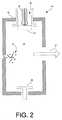
上述したようなイオンビーム源11の一例を挙げると、傍熱型の陰極40が挙げられる。図2は、傍熱型の陰極の実施形態を示す図である。このような構成は、水素、ヘリウム、酸素、および窒素の注入に利用され得る。本実施形態に係る傍熱型の陰極40は、アークチャンバ44の壁43を貫通して延伸している陰極41を有する。フィラメント45は、中空領域46内に陰極41に隣接して配設されている。電源(不図示)がフィラメント45を加熱して、フィラメント45と陰極41との間にバイアス電圧を印加して、陰極41とアークチャンバ44との間にアーク電圧を印加する。 An example of the ion beam source 11 as described above is an indirectly
フィラメント45は、加熱されると、フィラメント45の一部から電子を放出するのに十分なエネルギーを生成して、放出された電子はバイアス電圧によって陰極41の中空領域46へと推進される。この結果、陰極41は昇温させられて、最終的にはアークチャンバ44内に電子を放出し始める。電子は、アーク電圧によってアークチャンバ44内に引き込まれ、ソースガス47が供給するガス分子に衝突すると、プラズマを形成する。一部の実施形態によると、陰極41と壁43との間には、電圧ギャップを維持するべく間隙が設けられている。傍熱型の陰極40を利用するためには、ソースガス47をアークチャンバ44に導入する。一部の実施形態では、陰極41と壁43との間の間隙を小さく留めることによって、この間隙内にソースガス47が流入しないように厳しく制限している。一部の実施形態では制限部材が利用されるとしてよい。陰極41は、ソースガス47をイオン化するべく加熱される。ソースガス47をイオン化して、イオンビーム12を生成する。 When the
効率を高めると共にイオン生成を促進するべく、傍熱型の陰極40は、リペラ50に結合され得る。リペラ50は、機械素子、静電素子、または、磁気素子であってよく、傍熱型の陰極40によって生成された電子がアークチャンバ44を通過した後に当該電子を捕獲して、アークチャンバ44を再度通過するように電子を戻す。このような構成とすることによって、生成された電子とソースガス47とが衝突する可能性が高くなる。 An indirectly
図3は、マイクロ波イオン源の実施形態を示す図である。マイクロ波電力は、イオンビーム源11内でプラズマを生成するべく利用されるとしてよい。マイクロ波電力を利用することによって、フィラメントまたは陰極を設ける必要がなくなる。このため、マイクロ波電力は、長寿命であるとしてよい。マイクロ波電力を生成する方法の1つを挙げると、プラズマチャンバ内で約0.1テスラ(1kG)の軸方向磁場を生じさせる。発生した磁場は、以下の式で与えられる共鳴条件を持つ。
この具体的な実施形態によると、マイクロ波イオン源60は、少なくとも500Wの電力を供給する2.45GHzのマイクロ波生成器67によって駆動される。このようなマイクロ波生成器67は、磁電管である。入力電力が500Wの場合、電子密度が約E12cm−3からE13cm−3のプラズマが形成されるとしてよい。引出ビーム電流量は、プラズマチャンバ61の圧力がサブmTorrの範囲にある場合、約100mA/cm2から200mA/cm2であるとしてよい。According to this specific embodiment, the microwave ion source 60 is driven by a 2.45 GHz microwave generator 67 that supplies at least 500 W of power. Such a microwave generator 67 is a magnetoelectric tube. When the input power is 500 W, plasma having an electron density of about E12 cm−3 to E13 cm−3 may be formed. Extraction beam current, when the pressure in the
2.45GHzマイクロ波生成器の場合、電子の共鳴条件を満たすのは8.75E−2テスラの磁場の周波数である。このような磁場の作用によって、マイクロ波イオン源60は、電子サイクロトロン共鳴(ECR)源となるが、利用可能なビーム電流量は、共鳴値以上に磁場を大きくすることによって、大きくなり得る。In the case of the 2.45 GHz microwave generator, it is the frequency of the magnetic field of 8.75E-2 Tesla that satisfies the electron resonance condition. Due to the action of such a magnetic field, the microwave ion source 60 becomes an electron cyclotron resonance (ECR) source, but the amount of available beam current can be increased by increasing the magnetic field above the resonance value.
イオンは、マイクロ波イオン源60のプラズマチャンバ61で生成される。プラズマチャンバ61は通常、水で冷却されるシリンダーで、本実施形態では、直径が約2cmから5cmで、長さが約7cmから15cmである。プラズマチャンバ61は、アルミニウムまたはステンレススチールのような材料から形成されているとしてよく、一部の実施形態によると、二重壁となっている。プラズマチャンバ61を水で冷却することによって、マイクロ波イオン源60の機能は、低温表面で凝結しない材料からイオンを生成することに限定される。このような材料には、H2、He、N2、またはO2がある。しかし、マイクロ波イオン源60では、固体材料を利用するとしてもよい。Ions are generated in the
マイクロ波電力は、誘電体窓63を介して、プラズマチャンバ61内のプラズマ62に導入される。誘電体窓63は、プラズマチャンバ61の低圧と、大気とを分離している。しかし、マイクロ波電力はさらに、アンテナ等の当業者に公知のその他の手段によって、プラズマ62に導入されるとしてもよい。マイクロ波電力は、近共鳴条件によって、プラズマ62に吸収され得る。 The microwave power is introduced into the
誘電体窓63は通常、石英、アルミナ、または、窒化ホウ素等の複数の材料から形成され、誘電率が空気の誘電率からプラズマ62の誘電率へと段階的に変化するように選択される。これらの複数の材料は、サンドイッチ状または積層構造で配列されるとしてよい。このように段階的に変化させることによって、マイクロ波反射電力が最小限に抑えられる。本実施形態に係る誘電体窓63の寿命は、誘電体窓63を構成する複数の材料のうち、最終層によって決まる。これは、この最終層が、逆流する電子と衝突するためである。誘電体窓63のこの最終層は、予防メインテナンスまたはイオン源メインテナンスの際に交換されるとしてよい。 The
導波路68は、誘電体窓63に接触するように配設される。導波路68は、反射電力を最小限に抑えるスリー・スタブ・チューナーを含むとしてよく、特定のモードで動作する。 The waveguide 68 is disposed so as to contact the
軸方向磁場は、プラズマチャンバ61の周囲に配設されている複数のソレノイド64によって生成される。各ソレノイド64は通常、複数のコイルから構成されており、プラズマチャンバ61内の位置の関数として磁場が調整され得る。ビーム電流量を最大化すると共にビームノイズを最小化するべく、ソレノイド64を微調整するとしてよい。 The axial magnetic field is generated by a plurality of solenoids 64 disposed around the
ガス供給システム69は通常、プラズマチャンバ61に対してガスフローを供給する。一例を挙げると、このガスフローは、毎分当たり数立方センチメートルと小さい。ガスフローは、レギュレータ70から供給されるとしてよい。その他の低圧ガスソースを利用するとしてもよい。例えば、「セーフ・デリバリー・システム(Safe Delivery System)」コンテナまたはその他の当業者に公知のソースを利用するとしてもよい。 The gas supply system 69 normally supplies a gas flow to the
イオンは一般的に、プラズマチャンバ61の、マイクロ波電力の導入箇所とは反対側から引き出される。このため、イオンは通常、誘電体窓63とは反対側から引き出される。引出電極アセンブリ65は通常、プラズマスリット66の下流に位置する領域における漏れ磁場を最小限に抑えるべく軟鋼から形成されるが、当業者に公知のその他の材料から形成されるとしてもよい。 Ions are generally extracted from the opposite side of the
一部の実施形態では、引出電極アセンブリ65にリターンスチール71が含まれるとしてもよい。リターンスチール71は、プラズマチャンバ61の内部の強磁場を短絡させる。リターンスチール71は、軟鋼から形成されており、力線が真空ではなくスチールを通過するので、力線を捕獲する。リターンスチール71は、プラズマチャンバ61から放出されるイオンを偏向してしまう、引出領域近傍の磁場の発生を抑制する。一部の実施形態によると、引出電極アセンブリ65はさらに、サプレッション電極および接地電極を有するとしてよい。 In some embodiments, the
別の実施形態によると、イオンビーム源11には、RFイオン源が利用されるとしてよい。このようなRFイオン生成器は、当業者には公知であるように、高周波によってプラズマを生成する。このようなプラズマの生成は、プラズマ生成チャンバの外部にある外部アンテナによって行われるとしてもよいし、または、プラズマ生成チャンバの内部にある内部アンテナによって行われるとしてもよい。一実施形態に係るRFイオン源は、誘導結合を利用する。 According to another embodiment, the ion beam source 11 may be an RF ion source. Such RF ion generators generate plasma with a high frequency, as is known to those skilled in the art. Such plasma generation may be performed by an external antenna outside the plasma generation chamber, or may be performed by an internal antenna inside the plasma generation chamber. An RF ion source according to one embodiment utilizes inductive coupling.
図4は、静電チャックの実施形態を示す図である。チャック32は、静電力によって処理対象物26を固定および支持する。本実施形態に係るチャック32は、単一の処理対象物26を固定および支持するように構成されている。SOI構造を製造するためのイオン注入は通常、摂氏100度以上のイオン注入を行えるようにチャック32のようなチャックを必要とする。一部の実施形態によると、チャック32は、前述した温度における湾曲(bowing)の問題を最小限に抑えるか解消するように設計されている。 FIG. 4 is a diagram showing an embodiment of the electrostatic chuck. The
本実施形態によると、チャック32は、誘電層81と、導電電極82および83とを有する。2つの電極82および83を図示しているが、チャック32が有する電極の数は1つのみとしてもよいし、または3つ以上としてもよい。電極82および83は、DC電源またはAC電源84に電気接続されているとしてよい。 According to the present embodiment, the
チャック32のような静電チャックは一般的に、クーロン力型またはジョンソン・ラベック型に分類され得る。クーロン力型およびジョンソン・ラベック型の両方の原理を1つのチャックに組み込むとしてもよい。どちらのタイプのチャックも、処理対象物26と電極82および83との間に配置される誘電層81を有するとしてよい。電極82および83には、AC電圧またはDC電圧が印加されるとしてよい。 An electrostatic chuck, such as
誘電層81は、さまざまな絶縁体材料によって形成されるとしてよく、例えば、アルミナ等のセラミック材料から形成されるとしてよい。クーロン力型チャックの誘電層は、クーロン力型チャックの電荷が常に、電極と、クランプされている処理対象物とにあるように、電荷移動を禁止している。これとは対照的に、ジョンソン・ラベック型チャックの誘電層は、誘電層を介して電荷移動を可能としている。ジョンソン・ラベック型チャックの電荷移動に影響を与える要因には、誘電層の厚み、表面形状、および誘電層の表面の粗度が含まれ得る。誘電層を介した電荷移動によって、処理対象物と誘電層との間の界面に、電荷が蓄積される。クーロン力型チャックに比べてジョンソン・ラベック型チャックでは、互いに反対の電荷の間の距離が小さいので、クランプ電圧を同一とすると、クランプ圧はジョンソン・ラベック型チャックの方が大きくなる。 The dielectric layer 81 may be formed of various insulator materials, for example, a ceramic material such as alumina. The dielectric layer of the Coulomb force chuck inhibits charge transfer so that the charge of the Coulomb force chuck is always on the electrode and the object being clamped. In contrast, the dielectric layer of the Johnson-Rabeck chuck allows charge transfer through the dielectric layer. Factors affecting the charge transfer of a Johnson-Labeck chuck can include dielectric layer thickness, surface shape, and surface roughness of the dielectric layer. Due to the charge transfer through the dielectric layer, charge is accumulated at the interface between the object to be processed and the dielectric layer. The Johnson-Labeck chuck has a smaller distance between the opposite charges compared to the Coulomb force-type chuck. Therefore, if the clamp voltage is the same, the Johnson-Rabeck chuck has a higher clamping pressure.
通常は、チャック32が動作する温度範囲は、ドーピングレベルによって決まる。チャック32がジョンソン・ラベック型チャックの場合、ジョンソン・ラベック効果が異なる温度で発生すると共に誘電層81が伝導する電流範囲が正しくなるように、ドーピングレベルを修正することができる。例えば、O+の注入は、約摂氏400度で行うとしてよく、さらに、仕上げの注入を約摂氏50度で行うとしてよい。別の例を挙げると、H+の注入は、室温で行うとしてよい。このため、ジョンソン・ラベック効果を発生させるように、イオン注入が設定され得る。Normally, the temperature range in which the
クランプ電圧を約1kVとした場合、ジョンソン・ラベック型チャックで許容される裏面ガスの圧力は30Torrから50Torrの範囲内である。この範囲内であれば、20kWの酸素イオン(O+)ビームが、処理対象物26の温度を、SIMOX式イオン注入に通常適切な摂氏400度に維持することができる。この様子は、温度と、チャックの裏面ガスのガス圧とを比較した一例を示す図5に図示されている。When the clamp voltage is about 1 kV, the pressure of the backside gas allowed by the Johnson-Rabeck chuck is in the range of 30 Torr to 50 Torr. Within this range, a 20 kW oxygen ion (O+ ) beam can maintain the temperature of the object to be processed at 400 degrees Celsius, which is usually appropriate for SIMOX ion implantation. This state is illustrated in FIG. 5 which shows an example in which the temperature is compared with the gas pressure of the backside gas of the chuck.
図6は、裏面ガスによる熱結合が可能なチャックの実施形態を示す図である。一部の実施形態において、チャック32は、裏面ガスによる熱結合を実現するべく裏面ガス装置を含むとしてよい。尚、ガスの原子または分子87が、処理対象物26とチャック32との間を流動している。ガスの原子または分子87は、チャック32の表面に当たって、チャック32の温度に応じた並進エネルギーおよび回転エネルギーを得る。チャック32の温度に対応するエネルギーは、原子または分子87と、当たった表面との間の結合を説明する適応係数に基づいて説明され得る。適応係数は、原子または分子87の詳細な特性(例えば、自由度)、および、原子または分子87が当たる表面の詳細な特性(例えば、粗度または固着係数)に応じて変化する。 FIG. 6 is a diagram showing an embodiment of a chuck that can be thermally coupled by the backside gas. In some embodiments, the
そして、熱化された原子または分子87は、処理対象物26とチャック32との間の間隙を反対側に移動する。処理対象物26とチャック32との間の距離が、原子または分子87の平均自由工程、または、衝突と衝突との間に移動する平均距離に比べて小さい場合、直接、反対側まで間隙を移動する。原子または分子が処理対象物26に到達すると、同じ熱化プロセスが処理対象物26についても発生する。処理対象物26がチャック32よりも高温である場合、原子または分子87は処理対象物26からエネルギーを吸収する。チャック32が処理対象物26よりも高温である場合、原子または分子87はチャック32からエネルギーを吸収する。原子または分子87が処理対象物26とチャック32との間を移動すると、2つの表面は同じ温度に近づいていく。このようにして、処理対象物26は昇温または降温させられるとしてよい。このような熱伝達の効率は、ガスの原子または分子87同士が衝突する回数が多いと、原子または分子同士の間でエネルギーを共有してしまうので、悪くなってしまう場合がある。一実施形態によると、処理対象物26は、約摂氏300度から摂氏600度の範囲内の温度となるように、昇温または降温させられるとしてよい。 Then, the heated atoms or
一例によると、約15Torrにおいて、N2分子の平均自由工程は約20μmである。ガス圧を高くすると、処理対象物26とチャック32との間で熱伝達を行う原子の数が多くなるが、平均自由工程も短くなる。このように、低圧では、熱伝達はガス圧に比例する。チャックと処理対象物とが分離する程度に平均自由工程が短くなる値まで圧力が高くなると、増加幅は縮小し始める。チャック32に処理対象物26をより近接させて保持することによって、高圧を利用するとしてよい。多くの場合において、クランプ圧は裏面ガス圧よりも高くなければならない。According to one example, at about 15 Torr, the mean free path of N2 molecules is about 20 μm. Increasing the gas pressure increases the number of atoms that transfer heat between the object to be processed 26 and the
チャックの外部に熱源を設けて、処理対象物26を加熱するとしてもよい。図7は、ウェハ加熱用ランプを利用する装置の実施形態を示す図である。この実施形態では、処理対象物26とチャック32との間の界面に裏面ガスを利用するとしてもよいし、利用しないとしてもよい。 A heat source may be provided outside the chuck to heat the
処理対象物26は、この熱の大半を反射または吸収する。熱の一部は伝達されるが、チャック32の誘電体は、処理対象物26ほどは高温にならない場合がある。熱源として、Ushio社製の2kWのQIH−240−2000のようなランプ90を少なくとも1つ設けるとしてよい。熱源は、さまざまな波長のレーザであってもよい。例えば、処理対象物26を加熱するべく、処理対象物26が高効率で吸収する波長として赤外線が選択されるとしてもよい。 The
本実施形態によると、3つのランプ90を有するランプアレイ91が図示されている。別の実施形態では、処理対象物26を均等に加熱するべく、11個のランプ90が設けられている。ランプ90は、直線状のランプで、互いに上下になるように配列されているが、円形の電球で、円状アレイまたは当業者に公知のその他の構成で配列されているとしてもよい。ランプ90は、反射体92の前方に実装される。 According to this embodiment, a
本実施形態によると、ランプ90は帯状ビーム24の軌道の下方に位置しており、垂直位置にある場合に処理対象物26を加熱する。水平加熱位置は、処理対象物26に対するクランプを停止して、裏面の損傷を低減するように、選択され得る。ランプ90は、帯状ビーム24の上方に配置することも可能であり、帯状ビーム24の上方および下方に配置することも可能であり、または、帯状ビーム24が照射される処理対象物26の箇所と同じ箇所を加熱するとしてもよい。本実施形態では、帯状ビーム24を用いてイオン注入を実行するが、同じプロセスを用いて別の形態のイオン注入を実行することもできる。一実施形態によると、ランプ90は、約摂氏300度から摂氏600度までの範囲内の温度まで処理対象物26を加熱する。 According to the present embodiment, the
通常のイオン注入においては、フォトレジストの残留物がランプ90を覆ってしまう場合がある。このような問題は、固体状のマスクが利用されるので、高温イオン注入では発生し得ない。一方、ポリマーベースのフォトレジストは摂氏100度を超えると劣化する。一部の実施形態では、このような問題が発生しないようにするべく、ランプアレイ91には、従来の室温でのイオン注入を実行するべくカバーを設けるとしてもよいし、または、フォトレジストのガス抜けによる蒸気がランプ90または反射体92において凝結しないように、機械的に移動するとしてもよい。一実施形態によると、ランプ90は、ランプ90または反射体92に堆積した汚染物質を焼失させるべく、昇温させられるとしてよい。これに代えて、別の実施形態によると、ランプ90の温度を蒸気が凝結する温度よりも常に高くなるように維持するとしてもよい。 In normal ion implantation, the photoresist residue may cover the
処理対象物26は、チャック32上に配設される。本実施形態によると、チャック32は、方向94にスキャナ機構93によって並進させられるとしてもよい。方向94とは、処理対象物26およびチャック32を、帯状ビーム24の経路からランプアレイ91による加熱用の位置まで移動させるための方向である。 The
本明細書で使用する用語および表現は、説明のために使用するものであり、本発明を限定するものではない。本明細書において特定の用語および表現を使用しても、図示および説明した特徴(または、その一部)の均等物を排除することを意図するものではなく、請求項の範囲内ではさまざまな変形が可能であると認められる。その他にも、変形例、変更例、および代替例が実施可能である。したがって、上述の説明は、本発明を例示するものに過ぎず、本発明を限定することを意図するものではない。 The terms and expressions used herein are used for the purpose of explanation and are not intended to limit the present invention. The use of specific terms and expressions herein is not intended to exclude equivalents of the features shown or described (or portions thereof), and various modifications are within the scope of the claims. Is recognized as possible. In addition, variations, modifications, and alternatives can be implemented. Accordingly, the foregoing description is merely illustrative of the invention and is not intended to limit the invention.
Claims (25)
Translated fromJapanese前記イオンビームから、所望されない種を除去する分析マグネットと、
裏面ガスによる熱結合を有する静電チャックと
を備え、
前記イオンは、酸素および窒素から成る群から選択され、前記所与の範囲は、酸素の場合約1E17cm−2から4E17cm−2までの範囲、酸素の場合約1cm−2から3E15cm−2までの範囲、および窒素の場合約1E17cm−2から2E18cm−2までの範囲から成る群から選択され、
前記静電チャックは、ドーズが前記所与の範囲にある前記イオンビームによってシリコン・オン・インシュレータ用のイオン注入を実行するべく1つの処理対象物を保持し、前記処理対象物を約摂氏300度から摂氏600度の範囲内の温度まで冷却する
イオン注入装置。An ion beam source that generates ions to form an ion beam with a dose within a given range;
An analysis magnet for removing unwanted species from the ion beam;
An electrostatic chuck having thermal coupling with a backside gas,
The ions are selected from the group consisting of oxygen and nitrogen, said given range is the range in the range from about 1E17 cm-2 to 4E17 cm-2 case of oxygen, from about1 cm -2 case of oxygen up to 3E15 cm-2 And in the case of nitrogen, is selected from the group consisting of about 1E17 cm−2 to 2E18 cm−2 ;
The electrostatic chuck holds one processing object to perform ion implantation for a silicon-on-insulator with the ion beam having a dose within the given range, and the processing object is held at about 300 degrees Celsius. To an ion implanter that cools to a temperature in the range of 600 degrees Celsius.
請求項1に記載のイオン注入装置。The ion implantation apparatus according to claim 1, wherein the ion beam is a belt-like beam, and the electrostatic chuck scans the one processing object in a one-dimensional manner.
請求項1に記載のイオン注入装置。The ion implantation apparatus according to claim 1, wherein the ion beam source includes an indirectly heated cathode type ion source.
請求項1に記載のイオン注入装置。The ion implantation apparatus according to claim 1, wherein the ion beam source includes a microwave ion source.
請求項1に記載のイオン注入装置。The ion implantation apparatus according to claim 1, wherein the ion beam source includes an inductively coupled RF ion source.
請求項1に記載のイオン注入装置。The ion implantation apparatus according to claim 1, wherein, prior to the ion implantation, the one object to be processed is preheated to a temperature within a range of about 300 degrees Celsius to 600 degrees Celsius.
請求項6に記載のイオン注入装置。The ion implantation apparatus according to claim 6, wherein the electrostatic chuck heats the one processing object in advance.
をさらに備える請求項6に記載のイオン注入装置。The ion implantation apparatus according to claim 6, further comprising at least one lamp that preheats the one processing object.
請求項1に記載のイオン注入装置。The ion implanter according to claim 1, wherein the thermal coupling by the backside gas realizes a backside gas pressure of at least about 15 Torr.
前記イオンビームから、所望されない種を除去する分析マグネットと、
裏面ガスによる熱結合を有する静電チャックと
を備え、
前記イオンは、水素およびヘリウムから成る群から選択され、前記所与の範囲は、水素の場合約5E15cm−2から8E16cm−2までの範囲、ヘリウムの場合約5E15cm−2から8E16cm−2までの範囲から成る群から選択され、
前記静電チャックは、ドーズが前記所与の範囲にある前記イオンビームによってシリコン・オン・インシュレータ用のイオン注入を実行するべく1つの処理対象物を保持し、前記処理対象物を約摂氏300度から摂氏600度の範囲内の温度まで冷却する
イオン注入装置。An ion beam source that generates ions to form an ion beam with a dose within a given range;
An analysis magnet for removing unwanted species from the ion beam;
An electrostatic chuck having thermal coupling with a backside gas,
The ions are selected from the group consisting of hydrogen and helium, the given range is the range in the range from about 5E15 cm-2 to 8E16cm-2 case of hydrogen, from about 5E15 cm-2 when helium to 8E16cm-2 Selected from the group consisting of
The electrostatic chuck holds one processing object to perform ion implantation for a silicon-on-insulator with the ion beam having a dose within the given range, and the processing object is held at about 300 degrees Celsius. To an ion implanter that cools to a temperature in the range of 600 degrees Celsius.
請求項10に記載のイオン注入装置。The ion implantation apparatus according to claim 10, wherein the ion beam is a belt-like beam, and the electrostatic chuck scans the one processing object in a one-dimensional manner.
請求項10に記載のイオン注入装置。The ion implantation apparatus according to claim 10, wherein the ion beam source includes an indirectly heated cathode type ion source.
請求項10に記載のイオン注入装置。The ion implantation apparatus according to claim 10, wherein the ion beam source includes a microwave ion source.
請求項10に記載のイオン注入装置。The ion implantation apparatus according to claim 10, wherein the ion beam source includes an inductively coupled RF ion source.
請求項10に記載のイオン注入装置。The ion implantation apparatus according to claim 10, wherein the one object to be processed is preheated to a temperature within a range of about 300 degrees Celsius to 600 degrees Celsius prior to ion implantation.
請求項15に記載のイオン注入装置。The ion implantation apparatus according to claim 15, wherein the electrostatic chuck heats the one processing object in advance.
をさらに備える請求項15に記載のイオン注入装置。The ion implantation apparatus according to claim 15, further comprising at least one lamp that preheats the one processing object.
請求項10に記載のイオン注入装置。The ion implanter according to claim 10, wherein the thermal coupling by the backside gas realizes a backside gas pressure of at least about 15 Torr.
約5E15cm−2から8E16cm−2のドーズの水素、約5E15cm−2から8E16cm−2のドーズのヘリウム、約1E17cm−2から4E17cm−2のドーズの酸素、約1cm−2から3E15cm−2のドーズの酸素、約1E17cm−2から2E18cm−2のドーズの窒素から成る群から選択されたイオンビームを形成する段階と、
前記イオンビームを分析して、所望されない種を除去する段階と、
裏面ガスによる熱結合を有する静電チャック上に、シリコン・オン・インシュレータを製造するべく1つの処理対象物を実質的に保持する段階と、
前記イオンビームを用いて、前記1つの処理対象物にイオン注入を行う段階と、
前記1つの処理対象物を、前記静電チャックを用いて、約摂氏300度から摂氏600度の範囲内の温度まで冷却する段階と
を備える方法。A method for performing ion implantation for silicon-on-insulator in a single-wafer ion implantation apparatus,
Dose of hydrogen from about 5E15cm-2 8E16cm-2, from about 5E15 cm-2 dose of helium 8E16cm-2, dose of oxygen from about 1E17 cm-2 4E17 cm-2, from about1 cm -2 dose of 3E15 cm-2 Forming an ion beam selected from the group consisting of oxygen, nitrogen at a dose of about 1E17 cm−2 to 2E18 cm−2 ;
Analyzing the ion beam to remove unwanted species;
Substantially holding a workpiece to produce a silicon-on-insulator on an electrostatic chuck having thermal coupling with a backside gas;
Performing ion implantation on the one object to be processed using the ion beam;
Cooling the one object to be processed to a temperature in the range of about 300 degrees Celsius to 600 degrees Celsius using the electrostatic chuck.
請求項19に記載の方法。The method of claim 19, wherein the ion beam is generated by an indirectly heated cathode ion source.
請求項19に記載の方法。The method of claim 19, wherein the ion beam is generated by a microwave ion source.
請求項19に記載の方法。The method of claim 19, wherein the ion beam is generated by an inductively coupled RF ion source.
をさらに備える請求項19に記載の方法。The method of claim 19, further comprising pre-heating the one object to be processed to a temperature in the range of about 300 degrees Celsius to 600 degrees Celsius using the electrostatic chuck.
をさらに備える請求項19に記載の方法。20. The method of claim 19, further comprising pre-heating the one object to be processed to a temperature in the range of about 300 degrees Celsius to 600 degrees Celsius using at least one lamp.
請求項19に記載の方法。The ion beam is a band beam, and the step of performing ion implantation on the one processing object using the band beam is performed by scanning the processing object in one dimension. the method of.
Applications Claiming Priority (2)
| Application Number | Priority Date | Filing Date | Title |
|---|---|---|---|
| US11/862,810US20090084988A1 (en) | 2007-09-27 | 2007-09-27 | Single wafer implanter for silicon-on-insulator wafer fabrication |
| PCT/US2008/076615WO2009042459A1 (en) | 2007-09-27 | 2008-09-17 | Single wafer implanter for silicon-on-insulator wafer fabrication |
Publications (1)
| Publication Number | Publication Date |
|---|---|
| JP2010541164Atrue JP2010541164A (en) | 2010-12-24 |
Family
ID=40507119
Family Applications (1)
| Application Number | Title | Priority Date | Filing Date |
|---|---|---|---|
| JP2010527029AWithdrawnJP2010541164A (en) | 2007-09-27 | 2008-09-17 | Single wafer ion implanter for manufacturing silicon-on-insulator wafers |
Country Status (6)
| Country | Link |
|---|---|
| US (1) | US20090084988A1 (en) |
| JP (1) | JP2010541164A (en) |
| KR (1) | KR20100072046A (en) |
| CN (1) | CN101802980A (en) |
| TW (1) | TW200924012A (en) |
| WO (1) | WO2009042459A1 (en) |
Cited By (2)
| Publication number | Priority date | Publication date | Assignee | Title |
|---|---|---|---|---|
| JP2019522870A (en)* | 2016-06-02 | 2019-08-15 | アクセリス テクノロジーズ, インコーポレイテッド | Wafer cooling method |
| JP2020043108A (en)* | 2018-09-06 | 2020-03-19 | 住重アテックス株式会社 | Method for manufacturing semiconductor device |
Families Citing this family (13)
| Publication number | Priority date | Publication date | Assignee | Title |
|---|---|---|---|---|
| US8436318B2 (en)* | 2010-04-05 | 2013-05-07 | Varian Semiconductor Equipment Associates, Inc. | Apparatus for controlling the temperature of an RF ion source window |
| US20110320030A1 (en)* | 2010-06-25 | 2011-12-29 | Varian Semiconductor Equipment Associates, Inc. | Thermal Control of a Proximity Mask and Wafer During Ion Implantation |
| CN102376518B (en)* | 2010-08-17 | 2014-07-09 | 上海凯世通半导体有限公司 | Ion implantation system and methods |
| US9024282B2 (en)* | 2013-03-08 | 2015-05-05 | Varian Semiconductor Equipment Associates, Inc. | Techniques and apparatus for high rate hydrogen implantation and co-implantion |
| US9177708B2 (en)* | 2013-06-14 | 2015-11-03 | Varian Semiconductor Equipment Associates, Inc. | Annular cooling fluid passage for magnets |
| US9384937B2 (en)* | 2013-09-27 | 2016-07-05 | Varian Semiconductor Equipment Associates, Inc. | SiC coating in an ion implanter |
| TW201517133A (en)* | 2013-10-07 | 2015-05-01 | Applied Materials Inc | Enabling high activation of dopants in indium-aluminum-gallium-nitride material system using hot implantation and nanosecond annealing |
| US20160217970A1 (en)* | 2015-01-28 | 2016-07-28 | Advanced Ion Beam Technology, Inc. | Ion implanter and method for ion implantation |
| DE102015109661A1 (en)* | 2015-06-17 | 2016-12-22 | Infineon Technologies Ag | A method of forming a semiconductor device and semiconductor device |
| CN109003919B (en)* | 2018-07-11 | 2020-11-03 | 上海华力微电子有限公司 | Feedback method of wafer processing technological parameters |
| CN111653515B (en)* | 2020-05-29 | 2022-12-27 | 华虹半导体(无锡)有限公司 | Silicon wafer back injection device and method for preventing wafer dropping |
| CN114322590B (en)* | 2020-09-30 | 2022-12-06 | 长鑫存储技术有限公司 | Condenser and semiconductor processing machine |
| CN112701026A (en)* | 2020-12-28 | 2021-04-23 | 泉芯集成电路制造(济南)有限公司 | Ion implanter and ion implantation system |
Family Cites Families (9)
| Publication number | Priority date | Publication date | Assignee | Title |
|---|---|---|---|---|
| US5898179A (en)* | 1997-09-10 | 1999-04-27 | Orion Equipment, Inc. | Method and apparatus for controlling a workpiece in a vacuum chamber |
| US6998353B2 (en)* | 2001-11-05 | 2006-02-14 | Ibis Technology Corporation | Active wafer cooling during damage engineering implant to enhance buried oxide formation in SIMOX wafers |
| US20040079289A1 (en)* | 2002-10-23 | 2004-04-29 | Kellerman Peter L. | Electrostatic chuck wafer port and top plate with edge shielding and gas scavenging |
| KR100485385B1 (en)* | 2002-12-17 | 2005-04-27 | 삼성전자주식회사 | Charge exchanger and ion implanter having the same |
| GB2432039B (en)* | 2004-01-09 | 2009-03-11 | Applied Materials Inc | Improvements relating to ion implantation |
| US7819981B2 (en)* | 2004-10-26 | 2010-10-26 | Advanced Technology Materials, Inc. | Methods for cleaning ion implanter components |
| JP4907077B2 (en)* | 2004-11-30 | 2012-03-28 | 株式会社Sen | Wafer processing apparatus, wafer processing method, and ion implantation apparatus |
| US7547897B2 (en)* | 2006-05-26 | 2009-06-16 | Cree, Inc. | High-temperature ion implantation apparatus and methods of fabricating semiconductor devices using high-temperature ion implantation |
| US20080188011A1 (en)* | 2007-01-26 | 2008-08-07 | Silicon Genesis Corporation | Apparatus and method of temperature conrol during cleaving processes of thick film materials |
- 2007
- 2007-09-27USUS11/862,810patent/US20090084988A1/ennot_activeAbandoned
- 2008
- 2008-09-17JPJP2010527029Apatent/JP2010541164A/ennot_activeWithdrawn
- 2008-09-17CNCN200880107324Apatent/CN101802980A/enactivePending
- 2008-09-17KRKR1020107008854Apatent/KR20100072046A/ennot_activeWithdrawn
- 2008-09-17WOPCT/US2008/076615patent/WO2009042459A1/enactiveApplication Filing
- 2008-09-23TWTW097136518Apatent/TW200924012A/enunknown
Cited By (4)
| Publication number | Priority date | Publication date | Assignee | Title |
|---|---|---|---|---|
| JP2019522870A (en)* | 2016-06-02 | 2019-08-15 | アクセリス テクノロジーズ, インコーポレイテッド | Wafer cooling method |
| JP6997108B2 (en) | 2016-06-02 | 2022-01-17 | アクセリス テクノロジーズ, インコーポレイテッド | Wafer cooling method |
| JP2020043108A (en)* | 2018-09-06 | 2020-03-19 | 住重アテックス株式会社 | Method for manufacturing semiconductor device |
| JP7094840B2 (en) | 2018-09-06 | 2022-07-04 | 住重アテックス株式会社 | Manufacturing method of semiconductor device |
Also Published As
| Publication number | Publication date |
|---|---|
| KR20100072046A (en) | 2010-06-29 |
| US20090084988A1 (en) | 2009-04-02 |
| TW200924012A (en) | 2009-06-01 |
| CN101802980A (en) | 2010-08-11 |
| WO2009042459A1 (en) | 2009-04-02 |
Similar Documents
| Publication | Publication Date | Title |
|---|---|---|
| JP2010541164A (en) | Single wafer ion implanter for manufacturing silicon-on-insulator wafers | |
| KR100351489B1 (en) | A method of forming a circuit and buried insulating layer in a semiconductor substrate | |
| US5136171A (en) | Charge neutralization apparatus for ion implantation system | |
| KR100797138B1 (en) | Complementary Metal Oxide Semiconductor Device, and Method of Forming Metal Oxide Semiconductor Device and Complementary Metal Oxide Semiconductor Device | |
| TWI242788B (en) | Electrostatic trap for particles entrained in an ion beam | |
| US7977628B2 (en) | System and method for reducing particles and contamination by matching beam complementary aperture shapes to beam shapes | |
| JP2013525977A (en) | Silaboran injection process | |
| CN1922707B (en) | Modulating ion beam current | |
| KR100583909B1 (en) | Ion Doping Device and Doping Method | |
| US5554853A (en) | Producing ion beams suitable for ion implantation and improved ion implantation apparatus and techniques | |
| JP3265227B2 (en) | Doping apparatus and doping method | |
| US7977652B2 (en) | Optical heater for cryogenic ion implanter surface regeneration | |
| WO2005117059A1 (en) | Charge neutralization device | |
| EP0487656B1 (en) | Charge neutralization apparatus for ion implantation system | |
| KR0143433B1 (en) | Ion implanter | |
| JP3265283B2 (en) | Doping apparatus and doping method | |
| KR100581154B1 (en) | Ion Doping Device and Doping Method | |
| JPH04315757A (en) | Ion implanter | |
| JP2003332255A (en) | Doping processor |
Legal Events
| Date | Code | Title | Description |
|---|---|---|---|
| A300 | Application deemed to be withdrawn because no request for examination was validly filed | Free format text:JAPANESE INTERMEDIATE CODE: A300 Effective date:20111206 |