JP2010539428A - Compact optical system for collecting, integrating and irradiating light energy - Google Patents
Compact optical system for collecting, integrating and irradiating light energyDownload PDFInfo
- Publication number
- JP2010539428A JP2010539428AJP2010524238AJP2010524238AJP2010539428AJP 2010539428 AJP2010539428 AJP 2010539428AJP 2010524238 AJP2010524238 AJP 2010524238AJP 2010524238 AJP2010524238 AJP 2010524238AJP 2010539428 AJP2010539428 AJP 2010539428A
- Authority
- JP
- Japan
- Prior art keywords
- waveguide
- concentrator
- light
- solar concentrator
- solar
- Prior art date
- Legal status (The legal status is an assumption and is not a legal conclusion. Google has not performed a legal analysis and makes no representation as to the accuracy of the status listed.)
- Pending
Links
- 230000003287optical effectEffects0.000titleclaimsdescription44
- 230000001678irradiating effectEffects0.000title1
- 238000012546transferMethods0.000claimsabstractdescription36
- 239000002131composite materialSubstances0.000claims4
- 238000005286illuminationMethods0.000abstractdescription3
- 230000008901benefitEffects0.000description6
- 238000004519manufacturing processMethods0.000description6
- 230000005540biological transmissionEffects0.000description5
- 230000008859changeEffects0.000description5
- 238000010586diagramMethods0.000description4
- 239000000463materialSubstances0.000description4
- 239000012141concentrateSubstances0.000description3
- 238000013461designMethods0.000description3
- 230000001965increasing effectEffects0.000description3
- 238000000034methodMethods0.000description3
- 238000010521absorption reactionMethods0.000description2
- 238000013459approachMethods0.000description2
- 238000006243chemical reactionMethods0.000description2
- 238000005253claddingMethods0.000description2
- 238000000576coating methodMethods0.000description2
- 230000007246mechanismEffects0.000description2
- 238000012986modificationMethods0.000description2
- 230000004048modificationEffects0.000description2
- 238000001228spectrumMethods0.000description2
- 239000011248coating agentSubstances0.000description1
- 230000000295complement effectEffects0.000description1
- 150000001875compoundsChemical class0.000description1
- 239000000446fuelSubstances0.000description1
- 239000011521glassSubstances0.000description1
- 230000002650habitual effectEffects0.000description1
- 230000001939inductive effectEffects0.000description1
- 238000009434installationMethods0.000description1
- 230000008569processEffects0.000description1
- 238000012545processingMethods0.000description1
- 230000001902propagating effectEffects0.000description1
- 238000004064recyclingMethods0.000description1
- 238000007789sealingMethods0.000description1
- 239000007787solidSubstances0.000description1
- 238000002834transmittanceMethods0.000description1
Images


Classifications
- H—ELECTRICITY
- H10—SEMICONDUCTOR DEVICES; ELECTRIC SOLID-STATE DEVICES NOT OTHERWISE PROVIDED FOR
- H10F—INORGANIC SEMICONDUCTOR DEVICES SENSITIVE TO INFRARED RADIATION, LIGHT, ELECTROMAGNETIC RADIATION OF SHORTER WAVELENGTH OR CORPUSCULAR RADIATION
- H10F77/00—Constructional details of devices covered by this subclass
- H10F77/40—Optical elements or arrangements
- H10F77/42—Optical elements or arrangements directly associated or integrated with photovoltaic cells, e.g. light-reflecting means or light-concentrating means
- H10F77/488—Reflecting light-concentrating means, e.g. parabolic mirrors or concentrators using total internal reflection
- H—ELECTRICITY
- H10—SEMICONDUCTOR DEVICES; ELECTRIC SOLID-STATE DEVICES NOT OTHERWISE PROVIDED FOR
- H10F—INORGANIC SEMICONDUCTOR DEVICES SENSITIVE TO INFRARED RADIATION, LIGHT, ELECTROMAGNETIC RADIATION OF SHORTER WAVELENGTH OR CORPUSCULAR RADIATION
- H10F19/00—Integrated devices, or assemblies of multiple devices, comprising at least one photovoltaic cell covered by group H10F10/00, e.g. photovoltaic modules
- H10F19/40—Integrated devices, or assemblies of multiple devices, comprising at least one photovoltaic cell covered by group H10F10/00, e.g. photovoltaic modules comprising photovoltaic cells in a mechanically stacked configuration
- F—MECHANICAL ENGINEERING; LIGHTING; HEATING; WEAPONS; BLASTING
- F24—HEATING; RANGES; VENTILATING
- F24S—SOLAR HEAT COLLECTORS; SOLAR HEAT SYSTEMS
- F24S23/00—Arrangements for concentrating solar-rays for solar heat collectors
- F—MECHANICAL ENGINEERING; LIGHTING; HEATING; WEAPONS; BLASTING
- F24—HEATING; RANGES; VENTILATING
- F24S—SOLAR HEAT COLLECTORS; SOLAR HEAT SYSTEMS
- F24S23/00—Arrangements for concentrating solar-rays for solar heat collectors
- F24S23/12—Light guides
- F—MECHANICAL ENGINEERING; LIGHTING; HEATING; WEAPONS; BLASTING
- F24—HEATING; RANGES; VENTILATING
- F24S—SOLAR HEAT COLLECTORS; SOLAR HEAT SYSTEMS
- F24S23/00—Arrangements for concentrating solar-rays for solar heat collectors
- F24S23/30—Arrangements for concentrating solar-rays for solar heat collectors with lenses
- F—MECHANICAL ENGINEERING; LIGHTING; HEATING; WEAPONS; BLASTING
- F24—HEATING; RANGES; VENTILATING
- F24S—SOLAR HEAT COLLECTORS; SOLAR HEAT SYSTEMS
- F24S23/00—Arrangements for concentrating solar-rays for solar heat collectors
- F24S23/70—Arrangements for concentrating solar-rays for solar heat collectors with reflectors
- F24S23/79—Arrangements for concentrating solar-rays for solar heat collectors with reflectors with spaced and opposed interacting reflective surfaces
- H—ELECTRICITY
- H10—SEMICONDUCTOR DEVICES; ELECTRIC SOLID-STATE DEVICES NOT OTHERWISE PROVIDED FOR
- H10F—INORGANIC SEMICONDUCTOR DEVICES SENSITIVE TO INFRARED RADIATION, LIGHT, ELECTROMAGNETIC RADIATION OF SHORTER WAVELENGTH OR CORPUSCULAR RADIATION
- H10F77/00—Constructional details of devices covered by this subclass
- H10F77/40—Optical elements or arrangements
- H10F77/42—Optical elements or arrangements directly associated or integrated with photovoltaic cells, e.g. light-reflecting means or light-concentrating means
- H10F77/484—Refractive light-concentrating means, e.g. lenses
- F—MECHANICAL ENGINEERING; LIGHTING; HEATING; WEAPONS; BLASTING
- F24—HEATING; RANGES; VENTILATING
- F24S—SOLAR HEAT COLLECTORS; SOLAR HEAT SYSTEMS
- F24S50/00—Arrangements for controlling solar heat collectors
- F24S50/20—Arrangements for controlling solar heat collectors for tracking
- G—PHYSICS
- G02—OPTICS
- G02B—OPTICAL ELEMENTS, SYSTEMS OR APPARATUS
- G02B6/00—Light guides; Structural details of arrangements comprising light guides and other optical elements, e.g. couplings
- G02B6/0001—Light guides; Structural details of arrangements comprising light guides and other optical elements, e.g. couplings specially adapted for lighting devices or systems
- G02B6/0011—Light guides; Structural details of arrangements comprising light guides and other optical elements, e.g. couplings specially adapted for lighting devices or systems the light guides being planar or of plate-like form
- G02B6/0013—Means for improving the coupling-in of light from the light source into the light guide
- G02B6/0023—Means for improving the coupling-in of light from the light source into the light guide provided by one optical element, or plurality thereof, placed between the light guide and the light source, or around the light source
- G02B6/0028—Light guide, e.g. taper
- G—PHYSICS
- G02—OPTICS
- G02B—OPTICAL ELEMENTS, SYSTEMS OR APPARATUS
- G02B6/00—Light guides; Structural details of arrangements comprising light guides and other optical elements, e.g. couplings
- G02B6/0001—Light guides; Structural details of arrangements comprising light guides and other optical elements, e.g. couplings specially adapted for lighting devices or systems
- G02B6/0011—Light guides; Structural details of arrangements comprising light guides and other optical elements, e.g. couplings specially adapted for lighting devices or systems the light guides being planar or of plate-like form
- G02B6/0033—Means for improving the coupling-out of light from the light guide
- G02B6/0035—Means for improving the coupling-out of light from the light guide provided on the surface of the light guide or in the bulk of it
- G02B6/0045—Means for improving the coupling-out of light from the light guide provided on the surface of the light guide or in the bulk of it by shaping at least a portion of the light guide
- G02B6/0046—Tapered light guide, e.g. wedge-shaped light guide
- G02B6/0048—Tapered light guide, e.g. wedge-shaped light guide with stepwise taper
- Y—GENERAL TAGGING OF NEW TECHNOLOGICAL DEVELOPMENTS; GENERAL TAGGING OF CROSS-SECTIONAL TECHNOLOGIES SPANNING OVER SEVERAL SECTIONS OF THE IPC; TECHNICAL SUBJECTS COVERED BY FORMER USPC CROSS-REFERENCE ART COLLECTIONS [XRACs] AND DIGESTS
- Y02—TECHNOLOGIES OR APPLICATIONS FOR MITIGATION OR ADAPTATION AGAINST CLIMATE CHANGE
- Y02E—REDUCTION OF GREENHOUSE GAS [GHG] EMISSIONS, RELATED TO ENERGY GENERATION, TRANSMISSION OR DISTRIBUTION
- Y02E10/00—Energy generation through renewable energy sources
- Y02E10/40—Solar thermal energy, e.g. solar towers
- Y02E10/44—Heat exchange systems
- Y—GENERAL TAGGING OF NEW TECHNOLOGICAL DEVELOPMENTS; GENERAL TAGGING OF CROSS-SECTIONAL TECHNOLOGIES SPANNING OVER SEVERAL SECTIONS OF THE IPC; TECHNICAL SUBJECTS COVERED BY FORMER USPC CROSS-REFERENCE ART COLLECTIONS [XRACs] AND DIGESTS
- Y02—TECHNOLOGIES OR APPLICATIONS FOR MITIGATION OR ADAPTATION AGAINST CLIMATE CHANGE
- Y02E—REDUCTION OF GREENHOUSE GAS [GHG] EMISSIONS, RELATED TO ENERGY GENERATION, TRANSMISSION OR DISTRIBUTION
- Y02E10/00—Energy generation through renewable energy sources
- Y02E10/50—Photovoltaic [PV] energy
- Y02E10/52—PV systems with concentrators
- Y—GENERAL TAGGING OF NEW TECHNOLOGICAL DEVELOPMENTS; GENERAL TAGGING OF CROSS-SECTIONAL TECHNOLOGIES SPANNING OVER SEVERAL SECTIONS OF THE IPC; TECHNICAL SUBJECTS COVERED BY FORMER USPC CROSS-REFERENCE ART COLLECTIONS [XRACs] AND DIGESTS
- Y10—TECHNICAL SUBJECTS COVERED BY FORMER USPC
- Y10S—TECHNICAL SUBJECTS COVERED BY FORMER USPC CROSS-REFERENCE ART COLLECTIONS [XRACs] AND DIGESTS
- Y10S385/00—Optical waveguides
- Y10S385/90—Solar collector or transmitter
Landscapes
- Engineering & Computer Science (AREA)
- Chemical & Material Sciences (AREA)
- Life Sciences & Earth Sciences (AREA)
- Sustainable Development (AREA)
- Sustainable Energy (AREA)
- Thermal Sciences (AREA)
- Physics & Mathematics (AREA)
- Combustion & Propulsion (AREA)
- Mechanical Engineering (AREA)
- General Engineering & Computer Science (AREA)
- Photovoltaic Devices (AREA)
- Optical Elements Other Than Lenses (AREA)
- Investigating Or Analysing Materials By Optical Means (AREA)
- Microscoopes, Condenser (AREA)
Abstract
Translated fromJapaneseDescription
Translated fromJapanese[関連出願の相互参照]
本願は、2008年9月9日に出願された米国特許出願第12/207,346号に対する優先権を主張する。この346号特許出願は、2007年9月10日に出願された米国特許出願第11/852,854号に対する優先権を主張しており、この854号特許出願は、参照することによってその全体が本願に組み込まれる。[Cross-reference of related applications]
This application claims priority to US patent application Ser. No. 12 / 207,346, filed Sep. 9, 2008. This 346 patent application claims priority to US patent application Ser. No. 11 / 852,854 filed on Sep. 10, 2007, which is hereby incorporated by reference in its entirety. Incorporated in this application.
[発明の分野]
本発明は、電気的、熱的及び放射エネルギーを発生するためのソーラー・コンセントレータに関する。より詳細には、本発明は、複数のコンセントレータ・システムから太陽光を集中及び集約するために、屈折光学素子及び反射光学素子及び/又は転送光学素子の組合せを用いるソーラー・コンセントレータに関する。他の応用例には、小型光学素子を用いるライティングやイルミネーションが含まれる。[Field of the Invention]
The present invention relates to a solar concentrator for generating electrical, thermal and radiant energy. More particularly, the present invention relates to a solar concentrator that uses a combination of refractive and reflective and / or transfer optical elements to concentrate and aggregate sunlight from a plurality of concentrator systems. Other applications include lighting and illumination using small optical elements.
ソーラー・コレクタは、太陽光を収集及び集束するため、長期にわたって開発されてきた。周囲の太陽光のエネルギー密度を高めることにより、有用なエネルギー形態へのより効率的な変換が可能にされる。多数の形状とシステムが開発されてきたが、そのようなシステムは性能が平凡でありまた高額であるため、普及することができない。十分な性能と製造のし易さを実現するためには、太陽エネルギー・コレクタを改良する必要がある。 Solar collectors have been developed for a long time to collect and focus sunlight. Increasing the energy density of the surrounding sunlight allows for more efficient conversion to useful energy forms. Numerous shapes and systems have been developed, but such systems are unacceptable due to their mediocre and expensive performance. In order to achieve sufficient performance and ease of manufacture, the solar energy collector needs to be improved.
コンセントレータ・システムは、屈折部品及び/又は反射部品などの集束素子からなる光学素子の組合せを含み、反射及び/又は屈折素子は太陽光を光導波路に転送し、光導波路はレシーバ・ユニット(サーマル・ユニット及び/又は光起電性ユニット)及び他の従来のエネルギー変換システムに太陽光を効率的に集約及び集中するために、複数の階段状の反射面で構成されている。光導波路のアスペクト比と共に反射面の形状を制御することにより、太陽電池装置、ライトパイプ用途、熱交換器、燃料生成システム、スペクトル・スプリッタ(spectrum splitter)及び種々の光学用途に対する他の光の2次操作を含む種々の市販用途に対して、好ましくは連続領域に太陽光を容易に操作、収集及び集中することができる。 The concentrator system includes a combination of optical elements consisting of focusing elements such as refractive and / or reflective parts, where the reflective and / or refractive elements transfer sunlight to the optical waveguide, which is a receiver unit (thermal Unit and / or photovoltaic unit) and other conventional energy conversion systems in order to efficiently concentrate and concentrate sunlight into a plurality of stepped reflective surfaces. By controlling the shape of the reflective surface along with the aspect ratio of the light guide, solar cells, light pipe applications, heat exchangers, fuel generation systems, spectrum splitters and other light applications for various optical applications For various commercial applications including subsequent operations, sunlight can be easily manipulated, collected and concentrated, preferably in a continuous area.
本発明のこれらの及び他の目的、利点、及び応用例は、その動作の構成及び方法と共に添付した図面と合わせて考慮すれば、以下の詳細な説明から明らかになる。 These and other objects, advantages, and applications of the present invention will become apparent from the following detailed description when considered in conjunction with the accompanying drawings, together with the structure and method of operation thereof.
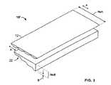
本発明の好ましい実施形態に基づいて構成された太陽エネルギー・コンセントレータ・システムは、図1では概略的に番号10で示されている。この太陽エネルギー・コンセントレータ・システム10は、光学集束素子12を備えている。この光学集束素子12は、対物レンズ、フレネルレンズ、及び/又は放物線又は複合形反射器のような反射面素子などの任意の従来の光学コンセントレータとすることができる。この光学集束素子12は、光14を小さな焦点領域16に集束させるように入射光14に対して動作する。好ましい実施形態では、この小さい焦点領域16は、反射部品又は転送部品18、又は全反射を生じさせる他の従来の光転送素子の中に配置される。この転送部品18は、集束光20を導波路22の中に転送する。導波路22は、スネルの法則に基づいて導波路22に沿って伝搬する光20が全反射するように構成される。ここで、全反射は、導波路22の表面24に入射する光20の角度が臨界角Φcよりも大きい場合に発生する。
Φc=sin(ηwaveguide/ηcladding)
ここで、Φc=全反射に対する臨界角
ηwaveguide=導波路材料の屈折率
ηcladding=クラッド層の屈折率又は周囲/導波路インターフェースにおける指数A solar energy concentrator system constructed in accordance with a preferred embodiment of the present invention is shown generally at 10 in FIG. The solar
Φc = sin (ηwaveguide / ηcladding )
Where Φc = critical angle for total reflection
ηwaveguide = refractive index of waveguide material
index in the refractive index or ambient / waveguide interface etacladding = clad layer
レシーバ26が導波路22の端部に配置され、光20を受け入れて有用なエネルギー又は他の光学用途のために処理する。 A
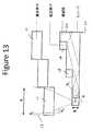
図13は、この機構部の細部が付いた、システム10の好ましい形態を例示している。複数のN個の集束素子12と転送素子18が示されている。集束素子12のそれぞれは、領域Aから半角θ1で入射光14を取り込み、この光14を集中度=A/Bとなるように半角θ2でより小さい領域Bに集束させる。転送素子18のそれぞれは、集束素子12の関連する1つからの集束光を受け取り、それをある角度ψで回転させ、かつそれを領域Bと半角θ2によって画定された集束レベルを維持しながら、導波路22の部分に挿入する。導波路22は、長さAで互いに間隔を空けた、高さBの増分段差(incremental step)を有する複数の部分から構成している。導波路22の各部分は転送素子18の関連する1つからの光を受け取り、導波路22が複数の集束素子14や転送素子18からの光を全体として集合して、その光14をレシーバ23が収集するように長さ方向に沿って伝搬させる。導波路22は与えられた集束レベルを変えないため、導波路22のアスペクト比は、
=導波路の高さ/導波路の長さ
=NxB/NxA
=B/A
=1/各素子内の集中度FIG. 13 illustrates a preferred form of
= Wave height / Wave length = NxB / NxA
= B / A
= 1 / concentration in each element
小型であることは、ソーラー・コンセントレータ(及び発光体などの他の装置)に対する大きな実際的な利点である。特に、使用される材料が少ないこと、難しいシールが必要な光学素子とレシーバ23との間の大きなエアギャップが除かれること、輸送や据付を安価にするために、装置がかさばらないこと、高価で危険を伴う習慣的な製造技術とは対照的に、従来の平坦なモジュール製造方法を利用できるという利点を有する。 The small size is a great practical advantage over solar concentrators (and other devices such as light emitters). In particular, less material is used, a large air gap between the optical element that requires difficult sealing and the
導波路22に関する小型化の限度は、レシーバ23によって規定される。このため、導波路22は、導波路が光を送るレシーバ23と同じ程度に小型化できるに過ぎない。たいていのコンセントレータでは、コンセントレータ12を小型化することは、レシーバ23の幅よりも影響が遙かに大きい。しかしながら、この装置は導波路22をそれぞれが送られた集束光の領域で規定される高さを有する部分から構成するため、集合された導波路22の高さはレシーバ23の高さに等しい。換言すると、導波路22の小型化は限定される。 The miniaturization limit for the
従って、本発明の構成に鑑みて、コンセントレータ・システム10によって実現される光の収束は、アスペクト比A/Bの関数であり、極めてコンパクトなコンセントレータ・システム10をもたらすことになる。この装置は比較的広い領域からの光を集めて、それを連続した領域を有するが高いコンパクト性を維持している比較的小さいレシーバに集束させることができる。これにより、必要な材料の体積を減らすことによって製造が単純化され、1つのモールドから複数のユニットを作ることが可能にされ、また構体の複雑性が低減される。 Thus, in light of the configuration of the present invention, the light convergence realized by the
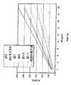
図12は、図2及び図6〜11に示された設計に対して実行された光線トレーシングの結果を示している。各設計は、A/Bの比率で示されるように、光を長さ寸法に集束させる能力に関して特定の性能を例示している。このデータは、±1度の入力された円錐状の半角、±20度の出力された円錐状の半角、初期の屈折率がn=1、そして最終的な屈折率がn=1.5の光に対するものである。これらの入力パラメータを有する理論的な最大許容集中度は長さ寸法では30xであるが、例えば図9では、25xの集光係数が達成されている。長さ寸法の集光係数がアスペクト比に比例するため、図9に示されている設計は、長さ(A)が250ミリメータで厚さ(B)がわずか10ミリメータのコンセントレータ、又は長さ(A)が500ミリメータで厚さ(B)がわずか20ミリメータのコンセントレータを与えることができる。これは比較的広い領域から集束光を効率的に集めて、それを1つのレシーバに与えることができる極めてコンパクトなコンセントレータ・システム10を示している。 FIG. 12 shows the results of ray tracing performed on the design shown in FIG. 2 and FIGS. Each design illustrates specific performance with respect to the ability to focus light into a length dimension, as indicated by the A / B ratio. This data is: ± 1 degree input conical half angle, ± 20 degree output conical half angle, initial refractive index n = 1, and final refractive index n = 1.5. It is for light. The theoretical maximum allowable concentration with these input parameters is 30x in the length dimension, but for example, in FIG. 9, a 25x condensing coefficient is achieved. The design shown in FIG. 9 is a concentrator with a length (A) of 250 millimeters and a thickness (B) of only 10 millimeters, or a length ( A concentrator with A) of 500 millimeters and a thickness (B) of only 20 millimeters can be provided. This illustrates a very
集束素子12と転送素子18の寸法と数は、コンセントレータ12の任意の入力開口に対して変えることができる。例えば、図13に示されているシステム10は、寸法が半分(A/2及びB/2)の2倍の数(2xN)の素子で実現することができる。集束素子12と転送素子18がより小さくかつ数が多くなるにつれて、コンセントレータ12の全体のアスペクト比は、1/集中度で与えられる導波路22のアスペクト比に近付く。言い換えると、集中度が10の場合、コンセントレータ12のアスペクト比を0.1にすることができる The size and number of focusing
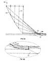
コンセントレータ12に対する代表的なアスペクト比は、およそ1の程度である。図14は屈折式コンセントレータ12を示しており、これは、例えば、対物レンズ又はフレネルレンズとすることができる。対物レンズの焦点距離が高さ25を画定する。集中度がA/Bで与えられるのに対して、アスペクト比は高さ/Aで与えられる。この値は、集中度よりも大きい。図15は、反射形式のコンセントレータ12に対する同様の状況を示している。 A typical aspect ratio for the
1つの集束素子に対する小型化の限界に到達することを目指した試みがなされてきた。図16は、1次及び2次反射光学素子を有するカセグレン式コンセントレータを示している。高さ/Aによって与えられたアスペクト比は0.25である。Winstonは、「Planar Concentrators Near the Etendue Limit」、2005年、の中で、「1/4アスペクト比に関する基本的な小型化の限界」について記載している。本発明との関連では、この小型化の限界は、集束素子12の個々の1つに適用される。複数の集束素子12から光を集める導波路22を使用することにより、1/4よりも小さくするように、また1/集中度に近付くようにシステム10を小型化することが可能にされる。 Attempts have been made to reach the limits of miniaturization for a single focusing element. FIG. 16 shows a Cassegrain concentrator having primary and secondary reflective optical elements. The aspect ratio given by height / A is 0.25. Winston, in “Planar Concentrators Near the Etendue Limit”, 2005, describes “basic miniaturization limits for 1/4 aspect ratio”. In the context of the present invention, this miniaturization limit applies to each individual focusing
本発明は、入力部からの光エネルギーをレシーバ23に配送する伝達効率にも利点がある。図13では、θ2は集束素子12によって制御される。θ2は導波路22の表面に当たる光によって作られる角度になり、また90−θ2は、導波路表面の法線に対して作られる角度である。上記のように、導波路22の中で全反射が生じるようにθ2を設定して、表面吸収損失をゼロまで減少することができる。The present invention also has an advantage in transmission efficiency for delivering light energy from the input unit to the
さらに、下記の特定の実施形態に示されているように、全反射を用いて光14を操作するように、集束素子12と転送素子18を設計することができる。また、固体誘導性媒体の中に光14のための連続した経路を設けるように、集束素子12、転送素子18及び導波路22を設計することができる。言い換えると、入力領域からレシーバ23に向かう光線は、反射コーティングや屈折率の変化のいずれにも遭遇しないことが必要である。反射コーティングは、約8%の吸収損失を引き起こす可能性がある。空気に対する屈折率1.5の光学材料(プラスチック又はガラス)の屈折率の変化は、約4%のフレネル反射による損失を発生する可能性がある。その結果、これらの損失の仕組みに対する伝達効率は、100%に達することができる。 Furthermore, the focusing
このことは、従来のコンセントレータ用光学素子とは著しく違っている。反射光学素子は、反射当たり8%の損失がある。このため、伝達効率は光学素子が1つの場合は約92%であり、2次反射光学素子が使用される場合は、約85%になる。屈折光学素子は、少なくとも1回の屈折率の変化が必要である。このため、伝達効率は光学素子が1つの場合は約96%であり、2次屈折光学素子が使用される場合は、約92%になる。 This is markedly different from conventional concentrator optical elements. The reflective optical element has a loss of 8% per reflection. Therefore, the transmission efficiency is about 92% when one optical element is used, and about 85% when a secondary reflective optical element is used. The refractive optical element needs to change the refractive index at least once. Therefore, the transmission efficiency is about 96% when one optical element is used, and about 92% when a second-order refractive optical element is used.
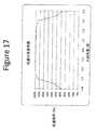
図17は、図13に示されている本発明の実施形態を通して、入力半角θ1の関数としての伝達効率を示している。この計算は、光線トレーシング用ソフトウェアに基づいている。この実施形態は、入力半角が±3度内で機能するように設計された。この効率は、フレネル反射とハード反射(hard reflection)による損失を考慮している。図示されているように、装置の効率は、θ1=0度では100%に近付き、±3度内ではほぼ100%に留まるが、その後急速に落ち込む。FIG. 17 shows the transmission efficiency as a function of the input half angle θ1 through the embodiment of the invention shown in FIG. This calculation is based on ray tracing software. This embodiment was designed so that the input half-angle functions within ± 3 degrees. This efficiency takes into account losses due to Fresnel reflection and hard reflection. As shown, the efficiency of the device approaches 100% at θ1 = 0 degrees, stays almost 100% within ± 3 degrees, but then falls off rapidly.
図2に示されているコンセントレータ・システム10の別の好ましい形態では、入射光14は、第1の段差では、前述された素子12を用いて集束又は合焦される。集束光20は、コンセントレータ・システム10のセクションを反射器/導波路セクション28に関連付けることによってさらに処理される。それぞれの反射器/導波路セクション28は反射セクション28を備えている。この反射セクション28は集束光20を受け取り、光30を関連する導波路セクション28の中に転送する。ここで、光30は全導波路22の長さに沿って全反射(TIR)される。複数の反射器/導波路セクション28は、階段状の構造の導波路22を有している。 In another preferred form of the
図18は、システム10の別の実施形態を示している。この実施形態では、導波路22はレシーバ23が配置されている、導波路22のベース面に向けて光14を転送する反射器27で終端する。コンセントレータの光学素子を、レシーバ23を組み入れる従来のレシーバ素子の面上に平坦に配置することは、製造上の利点がある。 FIG. 18 illustrates another embodiment of the
この構成では、図19に示されるように、コンセントレータ12を対称軸の周りにミラー化して、1つの単独のレシーバ23が配置されるように、両方の端部からの2つのレシーバ23が1つの連続した領域を形成することができる。この場合、開口領域が2倍になるがコンセントレータ12の厚さは変わらないため、小型化の限度は、1/(2x集中度)で与えられる。 In this configuration, as shown in FIG. 19, two
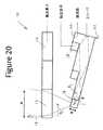
転送素子18は、光の経路を角度φだけ回転させる。図13では、φが90度であるように示されている。図20は、φ<90度であるように示している。これにより、1つの利点として、集束素子12を同じ面上に配置し、また転送素子18を同様に自身の面上に配置することができるため、製造を容易にすることができる。 The
集束素子12、転送素子18、及び関連する導波路22は大きさを変えることができ、図21はこの実施例を示している。ここで、A1、A2、及びA3は、B1、B2、及びB3と同様に長さが異なっている。しかしながら、集中度は、A1/B1=A2/B2などなどというように、各セクションで同じ状態のままである。導波路22のアスペクト比は、このため、下記の式によって与えられる。
=(B1+B2+B3)/(A1+A2+A3)
=1/集中度The focusing
= (B1 + B2 + B3) / (A1 + A2 + A3)
= 1 / concentration
図22に示されている別の実施形態では、光31を逆に通過させることによって、システム10を光ディフューザとして使用することもできる。図22では、当初はレシーバ23であった光源33からの入力光は、導波路22を通って導かれ、転送素子18によって集束素子12に転送される。この集束素子12は、出力光をシステム10の上方に送る。応用例には、照明、バックライト、及び他の光拡散装置が含まれる。全体を通して、光を集束するために例示された光学素子は、光源に置き換えられる「レシーバ23」を用いる照明用にも使用できることは理解されたい。 In another embodiment shown in FIG. 22, the
種々の反射器/導波路セクション28の断面図は、コンセントレータ・システム10の様々な構成に対して基本的な構成単位を提供する。1つの代表的な市販用の実施形態が図3に示されている。そのアスペクト比はNxB/NxA、A/Bであり、A/Bに比例する領域集光係数(area concentration factor)又はエネルギー密度△Φを有している。ここで、NxAは導波路22の長さであり、NxBは最大厚さ(図2及び図3を参照のこと)である。最も好ましい実施形態では、厚さNxBは複数の増分段差高さBから構成されており、これはそれぞれの反射器/導波路セクション32からのTIR光に対してクリアな光経路を提供する。 The cross-sectional views of the various reflector /
図4は、コンセントレータ・システム10’を有する回転(又は軸方向)対称形状のコンセントレータ・システム10の別の実施例を例示している。このコンセントレータ・システム10’は、導波路22の反射器/導波路セクション28に関連した集束素子12を有している。コンセントレータ・システム10’(すなわち、システム10)のこの回転対称形状は、円全体の任意の部分とすることができ、入射光14に対して三次元の径方向集束を可能にして、△Φにおいて(A/B)2に比例する集中度を生じるため、収集及びコンセントレータの効率が著しく高められる。図4の最も好ましい実施形態では、図3の実施形態では1軸トラッキングが使用されているのに対して、2軸のソーラー・トラッキングが使用されていることである。FIG. 4 illustrates another embodiment of a rotationally (or axially)
図4は、2軸にわたって集束を実現する1つの方法を示しており、図23は別の方法を示している。ここで、直線対称の1次コンセントレータ12は、1つの軸に沿って集束された光をコンセントレータ12の側部にあるレシーバ23に送る。そこでは、第2の直線対称コンセントレータ37が、垂直軸に沿って配置されている。この2次コンセントレータ37は、第2の軸に沿って光を集束して、この光を末尾のレシーバ23に送る。 FIG. 4 shows one way to achieve focusing over two axes, and FIG. 23 shows another way. Here, the linearly symmetric
図24は、2軸にわたって集束を実現する第3の方法を示している。ここで、示されているコンセントレータ12は、図19で説明されたようにミラー対称である。この場合も前と同様に、直線対称の1次コンセントレータ12は1つの軸に沿って集束された光14を、コンセントレータ12のベースにあるレシーバ23に送る。そこでは、第2の直線対称コンセントレータ37が、垂直軸に沿って配置されている。この2次コンセントレータ37は、第2の軸に沿って光14を集束して、この光を末尾のレシーバ23に送る。 FIG. 24 shows a third way to achieve focusing over two axes. Here, the
図3及び図4の直線形及び回転形の実施形態に加えて、コンセントレータ・システム10’は、入射光14の方向に関連して導波路22の上及び/又は下に配置されることができる。そのような実施形態では、いくらかの光14は導波路22を通過し、コンセントレータ・システム10’によって導波路22の後方に転送される。これらのシステムの形態により、光のリサイクリングが可能にされるため、最終的な効率が向上され、また本願で説明された、集束用に反射形システムを使用することにより、従来の屈折形システムに対して光を集束する効率が増加される。 In addition to the linear and rotational embodiments of FIGS. 3 and 4, the
別の実施形態では、TIRを生じさせるために、反射素子18を導波路22に関して角度的に調整することができる。反射素子18は、種々の角度形状を有する導波路22の一体部分とすることができる(図5A及び図5Bを参照されたい)。素子18は、別個の素子38及び39とすることもできる(図5C及び図5Dを参照のこと)。さらに、反射素子18と関連する導波路22は、それぞれ図5Eと図5Fに示されているように、入り組んだ光コレクタ・パイプ42及び光転送部品43の形態を取ることもできる。 In another embodiment, the
前述されたコンセントレータ・システム10及び10’の形態は、節領域(nodal area)ではなく連続領域に集束光20を提供するため、太陽電池、さらに処理するためのライトパイプ、熱交換器、2次コンセントレータ及び光スペクトル・スプリッタ(light spectrum splitter)などの、様々な下流のレシーバ26に集束された太陽エネルギーを送ることが可能にされる。 The form of the
図6〜図11Bに示されているさらに別の一連の実施形態では、集束及び収集効率をさらに著しく高めるために、種々の構成部品を組み合わせて使用することができる。図6は、最も好ましい実施形態の中で、光52を曲面反射器(curved reflector)54に向ける曲面形集束素子(curved concentrating element)50を示している。この曲面反射器54は、光52を導波路22に送る。図7は、別の最も好ましい実施形態の中で、別の曲面形集束素子56を示している。この曲面形集束素子56は、光52をTIRによって導波路22の中に向ける2つのプレーナ面(planar surface)59及び60を有している。図8Aは、界面66で光52を転送し、曲面反射器68で光52を反射し、光52を光学部品64の下側反射面72間の界面70に集束させる、部分的に閉じた光学素子64を示している。図8Bの拡大図で最も良く分かるように、導波路22は反射面72にほぼ相補的に角度適合している。 In yet another set of embodiments shown in FIGS. 6-11B, various components can be used in combination to further significantly increase focusing and collection efficiency. FIG. 6 shows, in the most preferred embodiment, a curved concentrating
別の最も好ましい実施形態の中の図9Aは、図8Aと同様のシステムであるが、光学部品65が閉じており、(光パイプの形式で)拡張導波路74に接続されている。この拡張導波路74は、光52を集めて、それを導波路22の中に転送する(図9Bに最も良く示されている)。 FIG. 9A, in another most preferred embodiment, is a system similar to FIG. 8A, but with the
図10Aでは、光学素子76は閉じており、図10Bに最も良く示されているように、入射光52は個別の角度交差セクション(angular cross section)を有する反射面77から全反射で反射される。この角度交差セクションは、全反射した光を収集し、面80、81及び82で反射させて導波路22に入力することができる。 In FIG. 10A, the
図11Aでは、光学部品82は別の反射器84と協同して、光52を2つの異なる光源82及び84から導波路22に向けることにより、光学部品82の面86に入射する全ての光をさらに確実に収集できるようにする。この実施形態では、光学部品82及び84は、集束素子と反射素子の両方の役割を演じる。 In FIG. 11A,
図25では、曲面集束素子(curved concentrating element)12は、光14を転送素子18に向け、この転送素子18は光14を導波路22に送る。集束素子12と転送素子18は同じ物理的部分の2つの異なる構造体として示されているが、導波路22は、第1の部分に結合された第2の物理的部分として示されている。図26では、曲面集束素子12は、光14を次々に動作する2つの反射器(転送素子18)に向け、これらの反射器は光14を導波路22に送る。集束素子12、転送素子18、及び導波路22は、一緒に連結された別個の物理的部分として示されている。図27は、光14を図26と同様に導波路22に向ける。しかしながら、転送素子18と導波路22は1つの構成の中に組み合わされている。 In FIG. 25, a curved concentrating
本発明の実施形態に関する前述の説明は、例示及び説明するために行われたものである。その説明は完全なものではなく、本発明を開示された詳細な形態に限定するものではない。修正及び変更は上記の教義に照らして可能であるか、又は本発明を実行することから得ることができる。当業者が本発明を種々の実施形態の中で、また考えられた特定の使用に適合するように種々の変形例を用いて使用できるように、本発明の原理及びその実際的な応用例を説明するため、これらの実施形態が選択されて記述されている。 The foregoing descriptions of the embodiments of the present invention have been presented for purposes of illustration and description. It is not intended to be exhaustive or to limit the invention to the precise form disclosed. Modifications and changes are possible in light of the above doctrine or can be obtained from practicing the invention. The principles of the present invention and its practical applications so that those skilled in the art can use the present invention in various embodiments and with various modifications to suit the particular use envisaged. For purposes of explanation, these embodiments have been selected and described.
Claims (17)
Translated fromJapanese前記入射光を受け取り、前記光を転送する複数の増分段差を有する転送部品と、
長さに沿って前記複数の増分段差に結合された形状の導波路と
を具備する、ソーラー・コンセントレータであって、
前記導波路が、前記入射光をレシーバが収集するように伝搬し、前記レシーバの幅が前記導波路の高さの関数である、ソーラー・コンセントレータ。A concentrator element that collects incident light;
A transfer component having a plurality of incremental steps for receiving the incident light and transferring the light;
A solar concentrator comprising: a waveguide coupled to the plurality of incremental steps along a length;
A solar concentrator, wherein the waveguide propagates as the receiver collects the incident light, the width of the receiver being a function of the height of the waveguide.
Applications Claiming Priority (5)
| Application Number | Priority Date | Filing Date | Title |
|---|---|---|---|
| US11/852,854US7672549B2 (en) | 2007-09-10 | 2007-09-10 | Solar energy concentrator |
| US11/852,854 | 2007-09-10 | ||
| US12/207,346US7664350B2 (en) | 2007-09-10 | 2008-09-09 | Compact optics for concentration, aggregation and illumination of light energy |
| PCT/US2008/075737WO2009035986A2 (en) | 2007-09-10 | 2008-09-09 | Compact optics for concentration, aggregation and illumination of light energy |
| US12/207,346 | 2008-09-09 |
Publications (3)
| Publication Number | Publication Date |
|---|---|
| JP2010539428Atrue JP2010539428A (en) | 2010-12-16 |
| JP2010539428A6 JP2010539428A6 (en) | 2011-05-06 |
| JP2010539428A5 JP2010539428A5 (en) | 2011-09-29 |
Family
ID=40431910
Family Applications (1)
| Application Number | Title | Priority Date | Filing Date |
|---|---|---|---|
| JP2010524238APendingJP2010539428A (en) | 2007-09-10 | 2008-09-09 | Compact optical system for collecting, integrating and irradiating light energy |
Country Status (8)
| Country | Link |
|---|---|
| US (2) | US7664350B2 (en) |
| EP (1) | EP2201309A4 (en) |
| JP (1) | JP2010539428A (en) |
| KR (1) | KR101455892B1 (en) |
| CN (1) | CN101809377B (en) |
| AU (1) | AU2008299119B2 (en) |
| CA (1) | CA2698284C (en) |
| WO (1) | WO2009035986A2 (en) |
Cited By (3)
| Publication number | Priority date | Publication date | Assignee | Title |
|---|---|---|---|---|
| JP2013543150A (en)* | 2010-11-04 | 2013-11-28 | バニヤン エナジー インコーポレイテッド | Compact optical components for heat collection and lighting systems |
| JP2013543991A (en)* | 2010-10-28 | 2013-12-09 | バニヤン エナジー インコーポレイテッド | Turning optics for heat collection and lighting systems |
| US9335530B2 (en) | 2007-05-01 | 2016-05-10 | Morgan Solar Inc. | Planar solar energy concentrator |
Families Citing this family (71)
| Publication number | Priority date | Publication date | Assignee | Title |
|---|---|---|---|---|
| US9040808B2 (en)* | 2007-05-01 | 2015-05-26 | Morgan Solar Inc. | Light-guide solar panel and method of fabrication thereof |
| US9337373B2 (en) | 2007-05-01 | 2016-05-10 | Morgan Solar Inc. | Light-guide solar module, method of fabrication thereof, and panel made therefrom |
| US7672549B2 (en)* | 2007-09-10 | 2010-03-02 | Banyan Energy, Inc. | Solar energy concentrator |
| JP2010539428A (en)* | 2007-09-10 | 2010-12-16 | バンヤン エナジー,インコーポレイテッド | Compact optical system for collecting, integrating and irradiating light energy |
| WO2009063416A2 (en)* | 2007-11-13 | 2009-05-22 | Koninklijke Philips Electronics, N.V. | Thin and efficient collecting optics for solar system |
| TWI359961B (en)* | 2008-04-16 | 2012-03-11 | Univ Nat Taiwan Science Tech | Light-concentrating panel |
| US20100024805A1 (en)* | 2008-07-29 | 2010-02-04 | Genie Lens Technologies, Llc | Solar panels for concentrating, capturing, and transmitting solar energy in conversion systems |
| CN102216695B (en)* | 2008-09-19 | 2013-12-25 | 加利福尼亚大学董事会 | System and method for solar energy capture and related method of manufacturing |
| WO2010040053A1 (en)* | 2008-10-02 | 2010-04-08 | Richard Morris Knox | Solar energy concentrator |
| ES2364665B1 (en)* | 2008-11-12 | 2012-05-23 | Abengoa Solar New Technologies, S.A. | LIGHTING AND CONCENTRATION SYSTEM. |
| US7968790B2 (en)* | 2009-01-16 | 2011-06-28 | Genie Lens Technologies, Llc | Photovoltaic (PV) enhancement films for enhancing optical path lengths and for trapping reflected light |
| US8338693B2 (en)* | 2009-01-16 | 2012-12-25 | Genie Lens Technology, LLC | Solar arrays and other photovoltaic (PV) devices using PV enhancement films for trapping light |
| US8048250B2 (en)* | 2009-01-16 | 2011-11-01 | Genie Lens Technologies, Llc | Method of manufacturing photovoltaic (PV) enhancement films |
| US7904871B2 (en)* | 2009-01-16 | 2011-03-08 | Genie Lens Technologies, Llc | Computer-implemented method of optimizing refraction and TIR structures to enhance path lengths in PV devices |
| US20100294338A1 (en)* | 2009-02-20 | 2010-11-25 | Solaria Corporation | Large Area Concentrator Lens Structure and Method |
| WO2010124028A2 (en)* | 2009-04-21 | 2010-10-28 | Vasylyev Sergiy V | Light collection and illumination systems employing planar waveguide |
| WO2010127348A2 (en)* | 2009-05-01 | 2010-11-04 | Garrett Bruer | Device and method for converting incident radiation into electrical energy using an upconversion photoluminescent solar concentrator |
| WO2010131250A1 (en)* | 2009-05-14 | 2010-11-18 | Yair Salomon Enterprises Ltd. | Light collection system and method |
| US7817885B1 (en)* | 2009-06-24 | 2010-10-19 | University Of Rochester | Stepped light collection and concentration system, components thereof, and methods |
| US9246038B2 (en)* | 2009-06-24 | 2016-01-26 | University Of Rochester | Light collecting and emitting apparatus, method, and applications |
| US8189970B2 (en) | 2009-06-24 | 2012-05-29 | University Of Rochester | Light collecting and emitting apparatus, method, and applications |
| CN102483484A (en)* | 2009-06-24 | 2012-05-30 | 罗切斯特大学 | Dimpled light collection and concentration system, components thereof, and methods |
| DE102009032575A1 (en)* | 2009-07-10 | 2011-02-17 | Carl Zeiss Ag | Optical arrangement for deflecting and concentrating sunlight on solar cell in solar power plant, has plate aligned to light source so that light is transmitted to Fresnel-structure and enters through boundary surface to medium i.e. air |
| TWI409967B (en)* | 2009-07-13 | 2013-09-21 | Epistar Corp | Solar battery module and manufacturing method thereof |
| US8723016B2 (en)* | 2009-07-14 | 2014-05-13 | Honeywell International Inc. | Low profile solar concentrator |
| TWI482995B (en)* | 2009-07-20 | 2015-05-01 | Ind Tech Res Inst | Light collecting device and lighting equipment |
| EP2460186A1 (en)* | 2009-07-31 | 2012-06-06 | Technische Universiteit Eindhoven | Luminescent optical device and solar cell system with such luminescent optical device |
| CN102947745A (en)* | 2009-08-20 | 2013-02-27 | 光处方革新有限公司 | Stepped flow-line concentrators and collimators |
| WO2011153633A1 (en)* | 2010-06-11 | 2011-12-15 | Morgan Solar Inc. | Monolithic photovoltaic solar concentrator |
| TWI400812B (en)* | 2010-06-30 | 2013-07-01 | 晶元光電股份有限公司 | Solar battery module and electromagnetic wave collecting device thereof |
| CA2804359A1 (en) | 2010-07-06 | 2012-01-12 | Sudhir V. Panse | A device for collecting solar energy |
| US8735791B2 (en) | 2010-07-13 | 2014-05-27 | Svv Technology Innovations, Inc. | Light harvesting system employing microstructures for efficient light trapping |
| WO2012014088A2 (en) | 2010-07-30 | 2012-02-02 | Morgan Solar Inc. | Light-guide solar module, method of fabrication thereof, and panel made therefrom |
| CN102034886B (en)* | 2010-10-15 | 2012-05-23 | 北京工业大学 | Secondary spotlighting solar photovoltaic device |
| CN102544172B (en) | 2010-12-30 | 2015-10-21 | 财团法人工业技术研究院 | Concentrated solar light guide module |
| US9054252B1 (en)* | 2011-01-10 | 2015-06-09 | Bingwu Gu | Two-axis tracking Fresnel lens solar oven and stove |
| US8885995B2 (en) | 2011-02-07 | 2014-11-11 | Morgan Solar Inc. | Light-guide solar energy concentrator |
| US20120234371A1 (en)* | 2011-03-18 | 2012-09-20 | Tong Zhang | Incident angle dependent smart solar concentrator |
| US8928988B1 (en) | 2011-04-01 | 2015-01-06 | The Regents Of The University Of California | Monocentric imaging |
| RU2488149C2 (en)* | 2011-04-26 | 2013-07-20 | Денис Михайлович Афанасьев | Planar lightguide |
| WO2012169980A1 (en) | 2011-06-09 | 2012-12-13 | Selimoglu Ozgur | A waveguide for concentrated solar collectors and a solar collector thereof |
| US8970767B2 (en) | 2011-06-21 | 2015-03-03 | Qualcomm Mems Technologies, Inc. | Imaging method and system with angle-discrimination layer |
| US8847142B2 (en) | 2011-07-20 | 2014-09-30 | Hong Kong Applied Science and Technology Research Institute, Co. Ltd. | Method and device for concentrating, collimating, and directing light |
| US9108369B2 (en) | 2011-07-25 | 2015-08-18 | Microsoft Technology Licensing, Llc | Wedge light guide |
| KR101347785B1 (en)* | 2011-08-29 | 2014-01-10 | 정재헌 | An elliptical mirror optic condensing guide |
| US9097826B2 (en) | 2011-10-08 | 2015-08-04 | Svv Technology Innovations, Inc. | Collimating illumination systems employing a waveguide |
| KR20140129157A (en)* | 2012-02-17 | 2014-11-06 | 쓰리엠 이노베이티브 프로퍼티즈 컴파니 | Backlight system |
| US8328403B1 (en) | 2012-03-21 | 2012-12-11 | Morgan Solar Inc. | Light guide illumination devices |
| WO2013152532A1 (en)* | 2012-04-09 | 2013-10-17 | 河南思可达光伏材料股份有限公司 | Light-concentrating photovoltaic glass with linear fresnel lens patterns |
| CN103378199B (en)* | 2012-04-26 | 2018-11-16 | 常州亚玛顿股份有限公司 | Solar energy hot systems |
| US20130329451A1 (en)* | 2012-06-11 | 2013-12-12 | Falcon Lin | Surgical light with led light guiding and focusing structure and method |
| TWI468737B (en)* | 2012-11-08 | 2015-01-11 | Univ Nat Taiwan Science Tech | Layer upon layer of optical disk |
| US20150301267A1 (en)* | 2012-12-05 | 2015-10-22 | 3M Innovative Properties Company | Anamorphic optical package |
| US20140196785A1 (en)* | 2013-01-11 | 2014-07-17 | Industrial Technology Research Institute | Light concentration module |
| US9595627B2 (en) | 2013-03-15 | 2017-03-14 | John Paul Morgan | Photovoltaic panel |
| US9960303B2 (en) | 2013-03-15 | 2018-05-01 | Morgan Solar Inc. | Sunlight concentrating and harvesting device |
| WO2014138857A1 (en) | 2013-03-15 | 2014-09-18 | John Paul Morgan | Light panel, optical assembly with improved interface and light panel with improved manufacturing tolerances |
| US9714756B2 (en) | 2013-03-15 | 2017-07-25 | Morgan Solar Inc. | Illumination device |
| US9442241B2 (en) | 2013-03-15 | 2016-09-13 | Morgan Solar Inc. | Optics for illumination devices |
| CN104456980B (en)* | 2014-12-09 | 2017-07-28 | 中国科学院工程热物理研究所 | A kind of secondary condensation reflection and transmission type parabolic trough type solar thermal collector |
| TWI580887B (en)* | 2015-02-06 | 2017-05-01 | 飛立威光能股份有限公司 | Lighting system and manufacturing method thereof |
| CN104990285B (en)* | 2015-07-20 | 2017-12-08 | 滕万圆 | Free of sun tracking energy concentrator |
| US10541643B2 (en) | 2015-12-21 | 2020-01-21 | Raydyne Energy, Inc. | Two-axis solar concentrator system |
| EP3535519A4 (en) | 2016-11-03 | 2020-06-17 | Basf Se | Daylighting panel |
| US10955531B2 (en) | 2017-06-21 | 2021-03-23 | Apple Inc. | Focal region optical elements for high-performance optical scanners |
| WO2019024080A1 (en)* | 2017-08-04 | 2019-02-07 | 博立多媒体控股有限公司 | Vertical solar apparatus |
| US10473923B2 (en)* | 2017-09-27 | 2019-11-12 | Apple Inc. | Focal region optical elements for high-performance optical scanners |
| KR102116173B1 (en)* | 2018-01-12 | 2020-05-28 | 제트카베 그룹 게엠베하 | Lamp for vehicle and vehicle |
| US11550038B2 (en) | 2018-09-26 | 2023-01-10 | Apple Inc. | LIDAR system with anamorphic objective lens |
| WO2021002227A1 (en)* | 2019-07-01 | 2021-01-07 | 日本電気株式会社 | Light-receiving device |
| CN115603657B (en)* | 2022-09-21 | 2023-06-27 | 国网甘肃省电力公司经济技术研究院 | Non-tracking low-magnification concentrating solar power generation device and design method |
Citations (8)
| Publication number | Priority date | Publication date | Assignee | Title |
|---|---|---|---|---|
| US4344417A (en)* | 1980-10-21 | 1982-08-17 | Jan Malecek | Solar energy collector |
| JPH1012025A (en)* | 1996-06-21 | 1998-01-16 | Casio Comput Co Ltd | Light source device |
| JPH10289605A (en)* | 1997-04-16 | 1998-10-27 | Casio Comput Co Ltd | Surface light source device |
| JP2000155219A (en)* | 1998-11-20 | 2000-06-06 | Taiyo Yuden Co Ltd | Condenser |
| JP2004047753A (en)* | 2002-07-12 | 2004-02-12 | Bridgestone Corp | Solar cell with condensing element |
| WO2004114418A1 (en)* | 2003-06-23 | 2004-12-29 | Hitachi Chemical Co., Ltd. | Concentrating photovoltaic power generation system |
| WO2006064365A2 (en)* | 2004-12-17 | 2006-06-22 | Universal Biosensors Pty Ltd. | Electromagnetic radiation collector |
| JP2007218540A (en)* | 2006-02-17 | 2007-08-30 | Nagaoka Univ Of Technology | Solar collector, solar cell and solar collector using the same |
Family Cites Families (135)
| Publication number | Priority date | Publication date | Assignee | Title |
|---|---|---|---|---|
| US705778A (en)* | 1901-11-07 | 1902-07-29 | William Leggett Mccabe | Portable conveyer. |
| US3780722A (en)* | 1972-04-26 | 1973-12-25 | Us Navy | Fiber optical solar collector |
| US4029519A (en)* | 1976-03-19 | 1977-06-14 | The United States Of America As Represented By The United States Energy Research And Development Administration | Solar collector having a solid transmission medium |
| US4357486A (en) | 1978-03-16 | 1982-11-02 | Atlantic Richfield Company | Luminescent solar collector |
| US4266179A (en)* | 1979-02-27 | 1981-05-05 | Hamm Jr James E | Solar energy concentration system |
| US4411490A (en)* | 1980-08-18 | 1983-10-25 | Maurice Daniel | Apparatus for collecting, distributing and utilizing solar radiation |
| US4379944A (en)* | 1981-02-05 | 1983-04-12 | Varian Associates, Inc. | Grooved solar cell for deployment at set angle |
| US4863224A (en)* | 1981-10-06 | 1989-09-05 | Afian Viktor V | Solar concentrator and manufacturing method therefor |
| US4505264A (en)* | 1983-12-27 | 1985-03-19 | Universite Laval | Electromagnetic wave concentrator |
| US5353075A (en) | 1988-08-17 | 1994-10-04 | In Focus Systems, Inc. | Convertible flat panel display system |
| US5828427A (en) | 1990-06-11 | 1998-10-27 | Reveo, Inc. | Computer-based image display systems having direct and projection modes of viewing |
| US5050946A (en)* | 1990-09-27 | 1991-09-24 | Compaq Computer Corporation | Faceted light pipe |
| US5150960A (en)* | 1991-12-06 | 1992-09-29 | General Motors Corporation | Rear license plate illumination |
| US5146354A (en)* | 1991-05-07 | 1992-09-08 | Compaq Computer Corporation | LCD system with a backlight having a light source at a light pipe's edge and with the LCD enframed |
| JPH05142535A (en)* | 1991-08-29 | 1993-06-11 | Meitaku Syst:Kk | Incident light supply device for edge light panel |
| WO1993006509A1 (en) | 1991-09-27 | 1993-04-01 | Yasuhiro Koike | Light-scattering light guide and its manufacture, and applied optics apparatus thereof |
| JPH05127161A (en) | 1991-11-07 | 1993-05-25 | Rohm Co Ltd | Liquid crystal display device and its backlight |
| KR970008351B1 (en)* | 1991-12-03 | 1997-05-23 | 샤프 가부시끼가이샤 | Liquid crystal display |
| US5438484A (en)* | 1991-12-06 | 1995-08-01 | Canon Kabushiki Kaisha | Surface lighting device and a display having such a lighting device |
| JP2692025B2 (en)* | 1992-01-24 | 1997-12-17 | スタンレー電気株式会社 | Planar light emitter device |
| JP3025109B2 (en)* | 1992-03-11 | 2000-03-27 | シャープ株式会社 | Light source and light source device |
| US5237641A (en)* | 1992-03-23 | 1993-08-17 | Nioptics Corporation | Tapered multilayer luminaire devices |
| US5528720A (en)* | 1992-03-23 | 1996-06-18 | Minnesota Mining And Manufacturing Co. | Tapered multilayer luminaire devices |
| US6002829A (en)* | 1992-03-23 | 1999-12-14 | Minnesota Mining And Manufacturing Company | Luminaire device |
| US5303322A (en)* | 1992-03-23 | 1994-04-12 | Nioptics Corporation | Tapered multilayer luminaire devices |
| US5806955A (en) | 1992-04-16 | 1998-09-15 | Tir Technologies, Inc. | TIR lens for waveguide injection |
| JP2980776B2 (en)* | 1992-06-04 | 1999-11-22 | 東ソー株式会社 | Backlight |
| JP3136200B2 (en)* | 1992-07-22 | 2001-02-19 | 株式会社日立製作所 | Liquid crystal display |
| DE4227468C2 (en)* | 1992-08-20 | 2002-01-17 | Teves Gmbh Alfred | Electrical switch unit, in particular for controlling air conditioning systems in motor vehicles |
| US5323477A (en)* | 1992-08-24 | 1994-06-21 | Motorola, Inc. | Contact array imager with integral waveguide and electronics |
| JPH0695112A (en) | 1992-09-16 | 1994-04-08 | Hitachi Ltd | Prism plate and information display device formed by using this plate |
| US5339179A (en)* | 1992-10-01 | 1994-08-16 | International Business Machines Corp. | Edge-lit transflective non-emissive display with angled interface means on both sides of light conducting panel |
| US5359691A (en) | 1992-10-08 | 1994-10-25 | Briteview Technologies | Backlighting system with a multi-reflection light injection system and using microprisms |
| US5499165A (en)* | 1992-10-08 | 1996-03-12 | Holmes, Jr.; Lawrence | Transparent edge-lit lighting pane for displays |
| US5390276A (en)* | 1992-10-08 | 1995-02-14 | Briteview Technologies | Backlighting assembly utilizing microprisms and especially suitable for use with a liquid crystal display |
| US5432876C1 (en)* | 1992-10-19 | 2002-05-21 | Minnesota Mining & Mfg | Illumination devices and optical fibres for use therein |
| US5400224A (en)* | 1993-01-08 | 1995-03-21 | Precision Lamp, Inc. | Lighting panel |
| KR0158247B1 (en)* | 1993-01-19 | 1999-03-20 | 미따라이 하지메 | A light guide, an illuminating device having the light guide, and an image reading device and an information processing device having the illuminating device |
| JPH06314069A (en)* | 1993-03-03 | 1994-11-08 | Fujitsu Ltd | Lighting equipment |
| JP3051591B2 (en)* | 1993-03-05 | 2000-06-12 | 日本メジフィジックス株式会社 | Anti-adhesion agent for thallium-201 container |
| US6111622A (en)* | 1993-03-12 | 2000-08-29 | Ois Optical Imaging Systems, Inc. | Day/night backlight for a liquid crystal display |
| AU6524694A (en)* | 1993-03-29 | 1994-10-24 | Precision Lamp, Inc. | Flat thin uniform thickness large area light source |
| JP3781441B2 (en) | 1993-07-23 | 2006-05-31 | 康博 小池 | Light scattering light guide light source device and liquid crystal display device |
| US5485354A (en)* | 1993-09-09 | 1996-01-16 | Precision Lamp, Inc. | Flat panel display lighting system |
| US5455882A (en) | 1993-09-29 | 1995-10-03 | Associated Universities, Inc. | Interactive optical panel |
| ATE203836T1 (en)* | 1993-10-05 | 2001-08-15 | Tir Technologies Inc | LIGHT SOURCE FOR BACKLIGHTING |
| US5440197A (en)* | 1993-10-05 | 1995-08-08 | Tir Technologies, Inc. | Backlighting apparatus for uniformly illuminating a display panel |
| US6313892B2 (en) | 1993-10-05 | 2001-11-06 | Teledyne Lighting And Display Products, Inc. | Light source utilizing reflective cavity having sloped side surfaces |
| US6129439A (en) | 1993-11-05 | 2000-10-10 | Alliedsignal Inc. | Illumination system employing an array of multi-faceted microprisms |
| US5396350A (en)* | 1993-11-05 | 1995-03-07 | Alliedsignal Inc. | Backlighting apparatus employing an array of microprisms |
| US5428468A (en)* | 1993-11-05 | 1995-06-27 | Alliedsignal Inc. | Illumination system employing an array of microprisms |
| US5555329A (en)* | 1993-11-05 | 1996-09-10 | Alliesignal Inc. | Light directing optical structure |
| US5521725A (en)* | 1993-11-05 | 1996-05-28 | Alliedsignal Inc. | Illumination system employing an array of microprisms |
| US5477239A (en) | 1993-11-12 | 1995-12-19 | Dell Usa, L.P. | Front lighting system for liquid crystal display |
| US5390085A (en) | 1993-11-19 | 1995-02-14 | Motorola, Inc. | Light diffuser for a liquid crystal display |
| US5598281A (en)* | 1993-11-19 | 1997-01-28 | Alliedsignal Inc. | Backlight assembly for improved illumination employing tapered optical elements |
| US5479275A (en) | 1993-12-03 | 1995-12-26 | Ois Optical Imaging Systems, Inc. | Backlit liquid crystal display with integral collimating, refracting, and reflecting means which refracts and collimates light from a first light source and reflects light from a second light source |
| US5485291A (en)* | 1994-02-22 | 1996-01-16 | Precision Lamp, Inc. | Uniformly thin, high efficiency large area lighting panel with two facet grooves that are spaced apart and have light source facing facets with smaller slopes than the facets facing away from the light source |
| US5982540A (en)* | 1994-03-16 | 1999-11-09 | Enplas Corporation | Surface light source device with polarization function |
| CA2134902C (en) | 1994-04-07 | 2000-05-16 | Friedrich Bertignoll | Light diffusing apparatus |
| JP3538220B2 (en)* | 1994-05-25 | 2004-06-14 | 株式会社エンプラス | Corner light supply type surface light source device |
| US5671994A (en)* | 1994-06-08 | 1997-09-30 | Clio Technologies, Inc. | Flat and transparent front-lighting system using microprisms |
| US5692066A (en) | 1994-09-20 | 1997-11-25 | Neopath, Inc. | Method and apparatus for image plane modulation pattern recognition |
| US5506929A (en) | 1994-10-19 | 1996-04-09 | Clio Technologies, Inc. | Light expanding system for producing a linear or planar light beam from a point-like light source |
| AU4409496A (en)* | 1994-11-29 | 1996-06-19 | Precision Lamp, Inc. | Edge light for panel display |
| US5579134A (en) | 1994-11-30 | 1996-11-26 | Honeywell Inc. | Prismatic refracting optical array for liquid flat panel crystal display backlight |
| US5659643A (en)* | 1995-01-23 | 1997-08-19 | Minnesota Mining And Manufacturing Company | Notched fiber array illumination device |
| JP3251452B2 (en)* | 1995-01-31 | 2002-01-28 | シャープ株式会社 | Backlight device for liquid crystal display device |
| US5608837A (en)* | 1995-05-15 | 1997-03-04 | Clio Technologies, Inc. | Transmissive type display and method capable of utilizing ambient light |
| US5621833A (en)* | 1995-06-12 | 1997-04-15 | Lau; Ronnie C. | Superposition of two-dimensional arrays |
| US5631994A (en)* | 1995-08-23 | 1997-05-20 | Minnesota Mining And Manufacturing Company | Structured surface light extraction overlay and illumination system |
| US5877874A (en)* | 1995-08-24 | 1999-03-02 | Terrasun L.L.C. | Device for concentrating optical radiation |
| US6104454A (en)* | 1995-11-22 | 2000-08-15 | Hitachi, Ltd | Liquid crystal display |
| US5710793A (en)* | 1995-12-21 | 1998-01-20 | National Semiconductor Corporation | Error signal quantization method and hardware for mixed blind and decision directed equalization |
| US5905826A (en)* | 1996-01-24 | 1999-05-18 | Minnesota Mining And Manufacturing Co. | Conspicuity marking system including light guide and retroreflective structure |
| US6072551A (en)* | 1996-02-14 | 2000-06-06 | Physical Optics Corporation | Backlight apparatus for illuminating a display with controlled light output characteristics |
| US5838403A (en) | 1996-02-14 | 1998-11-17 | Physical Optics Corporation | Liquid crystal display system with internally reflecting waveguide for backlighting and non-Lambertian diffusing |
| DE19610816C2 (en)* | 1996-03-19 | 1999-02-04 | Ctx Opto Electronics Corp | Backlight system for a scoreboard |
| US5926601A (en)* | 1996-05-02 | 1999-07-20 | Briteview Technologies, Inc. | Stacked backlighting system using microprisms |
| US5914760A (en)* | 1996-06-21 | 1999-06-22 | Casio Computer Co., Ltd. | Surface light source device and liquid crystal display device using the same |
| US6005343A (en) | 1996-08-30 | 1999-12-21 | Rakhimov; Alexander Tursunovich | High intensity lamp |
| US5870156A (en)* | 1996-09-05 | 1999-02-09 | Northern Telecom Limited | Shadow mask for backlit LCD |
| US5854872A (en) | 1996-10-08 | 1998-12-29 | Clio Technologies, Inc. | Divergent angle rotator system and method for collimating light beams |
| JPH10221528A (en)* | 1996-12-05 | 1998-08-21 | Toyota Motor Corp | Solar cell equipment |
| US6473554B1 (en) | 1996-12-12 | 2002-10-29 | Teledyne Lighting And Display Products, Inc. | Lighting apparatus having low profile |
| DE69836042T2 (en)* | 1997-03-04 | 2007-02-22 | Matsushita Electric Industrial Co., Ltd., Kadoma | Linear lighting device |
| US6007209A (en) | 1997-03-19 | 1999-12-28 | Teledyne Industries, Inc. | Light source for backlighting |
| US6123431A (en)* | 1997-03-19 | 2000-09-26 | Sanyo Electric Co., Ltd | Backlight apparatus and light guide plate |
| EP0867747A3 (en)* | 1997-03-25 | 1999-03-03 | Sony Corporation | Reflective display device |
| US6879354B1 (en)* | 1997-03-28 | 2005-04-12 | Sharp Kabushiki Kaisha | Front-illuminating device and a reflection-type liquid crystal display using such a device |
| US6992733B1 (en)* | 1997-04-11 | 2006-01-31 | Micron Technology, Inc. | Backlighting system for an LCD |
| EP1015811B1 (en) | 1997-09-19 | 2001-06-20 | Decoma International Inc. | Optics for separation of high and low intensity light |
| US6021007A (en)* | 1997-10-18 | 2000-02-01 | Murtha; R. Michael | Side-collecting lightguide |
| US6057505A (en)* | 1997-11-21 | 2000-05-02 | Ortabasi; Ugur | Space concentrator for advanced solar cells |
| US6151089A (en) | 1998-01-20 | 2000-11-21 | Sony Corporation | Reflection type display with light waveguide with inclined and planar surface sections |
| US6497939B1 (en) | 1998-02-03 | 2002-12-24 | Nippon Zeon Co., Ltd. | Flat plate and light guide plate |
| JPH11259007A (en)* | 1998-03-10 | 1999-09-24 | Sony Corp | Reflection type display device |
| US6134092A (en) | 1998-04-08 | 2000-10-17 | Teledyne Lighting And Display Products, Inc. | Illumination device for non-emissive displays |
| JP3119241B2 (en)* | 1998-07-01 | 2000-12-18 | 日本電気株式会社 | Liquid crystal display |
| US6428198B1 (en)* | 1998-07-07 | 2002-08-06 | Alliedsignal Inc. | Display system having a light source separate from a display device |
| US6234656B1 (en)* | 1998-08-20 | 2001-05-22 | Physical Optics Corporation | Fiber optic luminaire |
| GB9905642D0 (en) | 1999-03-11 | 1999-05-05 | Imperial College | Light concentrator for PV cells |
| DE19924783C2 (en)* | 1999-05-29 | 2003-04-03 | Kurz Leonhard Fa | Optical device |
| US6244264B1 (en)* | 1999-06-09 | 2001-06-12 | Solar Enterprises, International, Llc | Non-imaging optical illumination system |
| US6623132B2 (en)* | 1999-08-11 | 2003-09-23 | North American Lighting, Inc. | Light coupler hingedly attached to a light guide for automotive lighting |
| JP2001127331A (en) | 1999-10-29 | 2001-05-11 | Sanyo Electric Co Ltd | Solar cell module |
| US6440769B2 (en)* | 1999-11-26 | 2002-08-27 | The Trustees Of Princeton University | Photovoltaic device with optical concentrator and method of making the same |
| US6347874B1 (en)* | 2000-02-16 | 2002-02-19 | 3M Innovative Properties Company | Wedge light extractor with risers |
| US6639349B1 (en) | 2000-06-16 | 2003-10-28 | Rockwell Collins, Inc. | Dual-mode LCD backlight |
| JP3932407B2 (en) | 2000-07-03 | 2007-06-20 | ミネベア株式会社 | Surface lighting device |
| JP2002289900A (en) | 2001-03-23 | 2002-10-04 | Canon Inc | Concentrating solar cell module and concentrating solar power generation system |
| US6738051B2 (en)* | 2001-04-06 | 2004-05-18 | 3M Innovative Properties Company | Frontlit illuminated touch panel |
| US6592234B2 (en)* | 2001-04-06 | 2003-07-15 | 3M Innovative Properties Company | Frontlit display |
| KR100765138B1 (en)* | 2001-04-09 | 2007-10-15 | 삼성전자주식회사 | Backlight Assembly and Liquid Crystal Display Using Same |
| US6957904B2 (en) | 2001-07-30 | 2005-10-25 | 3M Innovative Properties Company | Illumination device utilizing displaced radiation patterns |
| US6576887B2 (en)* | 2001-08-15 | 2003-06-10 | 3M Innovative Properties Company | Light guide for use with backlit display |
| KR100789138B1 (en)* | 2001-09-05 | 2007-12-27 | 삼성전자주식회사 | Lighting device and reflection type liquid crystal display device using the same |
| US6966684B2 (en) | 2001-09-13 | 2005-11-22 | Gelcore, Llc | Optical wave guide |
| US6804062B2 (en)* | 2001-10-09 | 2004-10-12 | California Institute Of Technology | Nonimaging concentrator lens arrays and microfabrication of the same |
| DE20200571U1 (en)* | 2002-01-15 | 2002-04-11 | FER Fahrzeugelektrik GmbH, 99817 Eisenach | vehicle light |
| US6796700B2 (en)* | 2002-02-02 | 2004-09-28 | Edward Robert Kraft | Flat panel luminaire with remote light source and hollow light pipe for back lit signage applications |
| US6986660B2 (en)* | 2002-06-04 | 2006-01-17 | Zimmer Dental, Inc. | Retaining screw with rententive feature |
| JP3923867B2 (en) | 2002-07-26 | 2007-06-06 | 株式会社アドバンスト・ディスプレイ | Planar light source device and liquid crystal display device using the same |
| US6842571B2 (en)* | 2002-09-05 | 2005-01-11 | Motorola, Inc. | Optical interconnect system with layered lightpipe |
| US7063449B2 (en)* | 2002-11-21 | 2006-06-20 | Element Labs, Inc. | Light emitting diode (LED) picture element |
| JP3767544B2 (en) | 2002-11-25 | 2006-04-19 | セイコーエプソン株式会社 | Optical device, illumination device, and projector |
| JP3776082B2 (en)* | 2002-12-19 | 2006-05-17 | シャープ株式会社 | Solar cell module |
| US7286296B2 (en)* | 2004-04-23 | 2007-10-23 | Light Prescriptions Innovators, Llc | Optical manifold for light-emitting diodes |
| US6966661B2 (en) | 2003-09-16 | 2005-11-22 | Robert L. Read | Half-round total internal reflection magnifying prism |
| JP4262113B2 (en)* | 2004-02-13 | 2009-05-13 | シチズン電子株式会社 | Backlight |
| US20060174867A1 (en) | 2004-12-28 | 2006-08-10 | Applied Optical Materials | Nonimaging solar collector/concentrator |
| EP1851106B1 (en) | 2005-02-10 | 2013-08-07 | Instapower Ltd. | A lighting device |
| EP2174058A4 (en)* | 2007-05-01 | 2011-10-26 | Morgan Solar Inc | LIGHTING DEVICE |
| JP2010539428A (en)* | 2007-09-10 | 2010-12-16 | バンヤン エナジー,インコーポレイテッド | Compact optical system for collecting, integrating and irradiating light energy |
| US7672549B2 (en) | 2007-09-10 | 2010-03-02 | Banyan Energy, Inc. | Solar energy concentrator |
- 2008
- 2008-09-09JPJP2010524238Apatent/JP2010539428A/enactivePending
- 2008-09-09WOPCT/US2008/075737patent/WO2009035986A2/enactiveApplication Filing
- 2008-09-09USUS12/207,346patent/US7664350B2/ennot_activeExpired - Fee Related
- 2008-09-09EPEP08830932Apatent/EP2201309A4/ennot_activeWithdrawn
- 2008-09-09AUAU2008299119Apatent/AU2008299119B2/ennot_activeCeased
- 2008-09-09KRKR1020107007127Apatent/KR101455892B1/ennot_activeExpired - Fee Related
- 2008-09-09CNCN2008801057847Apatent/CN101809377B/ennot_activeExpired - Fee Related
- 2008-09-09CACA2698284Apatent/CA2698284C/ennot_activeExpired - Fee Related
- 2010
- 2010-02-12USUS12/705,434patent/US7925129B2/ennot_activeExpired - Fee Related
Patent Citations (8)
| Publication number | Priority date | Publication date | Assignee | Title |
|---|---|---|---|---|
| US4344417A (en)* | 1980-10-21 | 1982-08-17 | Jan Malecek | Solar energy collector |
| JPH1012025A (en)* | 1996-06-21 | 1998-01-16 | Casio Comput Co Ltd | Light source device |
| JPH10289605A (en)* | 1997-04-16 | 1998-10-27 | Casio Comput Co Ltd | Surface light source device |
| JP2000155219A (en)* | 1998-11-20 | 2000-06-06 | Taiyo Yuden Co Ltd | Condenser |
| JP2004047753A (en)* | 2002-07-12 | 2004-02-12 | Bridgestone Corp | Solar cell with condensing element |
| WO2004114418A1 (en)* | 2003-06-23 | 2004-12-29 | Hitachi Chemical Co., Ltd. | Concentrating photovoltaic power generation system |
| WO2006064365A2 (en)* | 2004-12-17 | 2006-06-22 | Universal Biosensors Pty Ltd. | Electromagnetic radiation collector |
| JP2007218540A (en)* | 2006-02-17 | 2007-08-30 | Nagaoka Univ Of Technology | Solar collector, solar cell and solar collector using the same |
Cited By (3)
| Publication number | Priority date | Publication date | Assignee | Title |
|---|---|---|---|---|
| US9335530B2 (en) | 2007-05-01 | 2016-05-10 | Morgan Solar Inc. | Planar solar energy concentrator |
| JP2013543991A (en)* | 2010-10-28 | 2013-12-09 | バニヤン エナジー インコーポレイテッド | Turning optics for heat collection and lighting systems |
| JP2013543150A (en)* | 2010-11-04 | 2013-11-28 | バニヤン エナジー インコーポレイテッド | Compact optical components for heat collection and lighting systems |
Also Published As
| Publication number | Publication date |
|---|---|
| CA2698284C (en) | 2013-06-25 |
| CN101809377B (en) | 2013-07-24 |
| EP2201309A2 (en) | 2010-06-30 |
| CN101809377A (en) | 2010-08-18 |
| AU2008299119B2 (en) | 2012-06-14 |
| US20090067784A1 (en) | 2009-03-12 |
| US20100142891A1 (en) | 2010-06-10 |
| KR20100072005A (en) | 2010-06-29 |
| KR101455892B1 (en) | 2014-11-04 |
| WO2009035986A3 (en) | 2009-05-14 |
| US7664350B2 (en) | 2010-02-16 |
| AU2008299119A1 (en) | 2009-03-19 |
| WO2009035986A2 (en) | 2009-03-19 |
| WO2009035986A4 (en) | 2009-07-16 |
| CA2698284A1 (en) | 2009-03-19 |
| US7925129B2 (en) | 2011-04-12 |
| EP2201309A4 (en) | 2010-12-01 |
Similar Documents
| Publication | Publication Date | Title |
|---|---|---|
| JP2010539428A (en) | Compact optical system for collecting, integrating and irradiating light energy | |
| JP2010539428A6 (en) | Compact optical element that focuses, collects and illuminates light energy | |
| JP5944400B2 (en) | Compact optical components for heat collection and lighting systems | |
| US20090064993A1 (en) | Solar energy concentrator | |
| US9229144B2 (en) | Redirecting optics for concentration and illumination systems | |
| CN102313975B (en) | Light-gathering system | |
| TW201234631A (en) | Light concentrating device and method | |
| AU2012223120B2 (en) | Compact optics for concentration, aggregation and illumination of light energy | |
| Karp et al. | Radial coupling method for orthogonal concentration within planar micro-optic solar collectors | |
| CN119355938A (en) | A tracking-free concentrator composed of a light directional deflection prism combination | |
| O'Gallagher | Comparative performance features of different nonimaging secondary concentrators |
Legal Events
| Date | Code | Title | Description |
|---|---|---|---|
| A521 | Request for written amendment filed | Free format text:JAPANESE INTERMEDIATE CODE: A523 Effective date:20110811 | |
| A621 | Written request for application examination | Free format text:JAPANESE INTERMEDIATE CODE: A621 Effective date:20110811 | |
| A131 | Notification of reasons for refusal | Free format text:JAPANESE INTERMEDIATE CODE: A131 Effective date:20130107 | |
| A601 | Written request for extension of time | Free format text:JAPANESE INTERMEDIATE CODE: A601 Effective date:20130401 | |
| A602 | Written permission of extension of time | Free format text:JAPANESE INTERMEDIATE CODE: A602 Effective date:20130412 | |
| A521 | Request for written amendment filed | Free format text:JAPANESE INTERMEDIATE CODE: A523 Effective date:20130502 | |
| A131 | Notification of reasons for refusal | Free format text:JAPANESE INTERMEDIATE CODE: A131 Effective date:20131203 | |
| A601 | Written request for extension of time | Free format text:JAPANESE INTERMEDIATE CODE: A601 Effective date:20140303 | |
| A602 | Written permission of extension of time | Free format text:JAPANESE INTERMEDIATE CODE: A602 Effective date:20140310 | |
| A521 | Request for written amendment filed | Free format text:JAPANESE INTERMEDIATE CODE: A523 Effective date:20140603 | |
| A02 | Decision of refusal | Free format text:JAPANESE INTERMEDIATE CODE: A02 Effective date:20150120 | |
| A521 | Request for written amendment filed | Free format text:JAPANESE INTERMEDIATE CODE: A523 Effective date:20150518 | |
| A521 | Request for written amendment filed | Free format text:JAPANESE INTERMEDIATE CODE: A821 Effective date:20150519 | |
| A911 | Transfer to examiner for re-examination before appeal (zenchi) | Free format text:JAPANESE INTERMEDIATE CODE: A911 Effective date:20150609 | |
| A912 | Re-examination (zenchi) completed and case transferred to appeal board | Free format text:JAPANESE INTERMEDIATE CODE: A912 Effective date:20150821 | |
| A601 | Written request for extension of time | Free format text:JAPANESE INTERMEDIATE CODE: A601 Effective date:20160905 | |
| A601 | Written request for extension of time | Free format text:JAPANESE INTERMEDIATE CODE: A601 Effective date:20161011 | |
| A521 | Request for written amendment filed | Free format text:JAPANESE INTERMEDIATE CODE: A523 Effective date:20161109 |