JP2010538495A - Multi-junction solar cell - Google Patents
Multi-junction solar cellDownload PDFInfo
- Publication number
- JP2010538495A JP2010538495AJP2010524067AJP2010524067AJP2010538495AJP 2010538495 AJP2010538495 AJP 2010538495AJP 2010524067 AJP2010524067 AJP 2010524067AJP 2010524067 AJP2010524067 AJP 2010524067AJP 2010538495 AJP2010538495 AJP 2010538495A
- Authority
- JP
- Japan
- Prior art keywords
- solar cell
- substrate
- layer
- junction
- photovoltaic
- Prior art date
- Legal status (The legal status is an assumption and is not a legal conclusion. Google has not performed a legal analysis and makes no representation as to the accuracy of the status listed.)
- Pending
Links
- 239000000758substrateSubstances0.000claimsabstractdescription175
- 230000007547defectEffects0.000claimsabstractdescription90
- 239000004065semiconductorSubstances0.000claimsabstractdescription56
- 210000004027cellAnatomy0.000claimsdescription208
- 239000000463materialSubstances0.000claimsdescription146
- XUIMIQQOPSSXEZ-UHFFFAOYSA-NSiliconChemical compound[Si]XUIMIQQOPSSXEZ-UHFFFAOYSA-N0.000claimsdescription105
- 229910052710siliconInorganic materials0.000claimsdescription104
- 239000010703siliconSubstances0.000claimsdescription104
- 239000002178crystalline materialSubstances0.000claimsdescription35
- 238000000034methodMethods0.000claimsdescription28
- 239000013078crystalSubstances0.000claimsdescription16
- 230000003287optical effectEffects0.000claimsdescription12
- 150000001875compoundsChemical class0.000claimsdescription11
- 210000004692intercellular junctionAnatomy0.000claimsdescription6
- 230000015572biosynthetic processEffects0.000claimsdescription5
- 238000010276constructionMethods0.000claimsdescription2
- 239000010410layerSubstances0.000description182
- 229910000530Gallium indium arsenideInorganic materials0.000description61
- JBRZTFJDHDCESZ-UHFFFAOYSA-NAsGaChemical compound[As]#[Ga]JBRZTFJDHDCESZ-UHFFFAOYSA-N0.000description35
- 229910001218Gallium arsenideInorganic materials0.000description34
- GNPVGFCGXDBREM-UHFFFAOYSA-Ngermanium atomChemical compound[Ge]GNPVGFCGXDBREM-UHFFFAOYSA-N0.000description29
- 229910052732germaniumInorganic materials0.000description26
- 229910004298SiO 2Inorganic materials0.000description23
- VYPSYNLAJGMNEJ-UHFFFAOYSA-NSilicium dioxideChemical compoundO=[Si]=OVYPSYNLAJGMNEJ-UHFFFAOYSA-N0.000description22
- 238000010586diagramMethods0.000description20
- 229910052751metalInorganic materials0.000description14
- 239000002184metalSubstances0.000description14
- 238000004519manufacturing processMethods0.000description13
- KRHYYFGTRYWZRS-UHFFFAOYSA-NFluoraneChemical compoundFKRHYYFGTRYWZRS-UHFFFAOYSA-N0.000description11
- 235000012239silicon dioxideNutrition0.000description11
- 239000000377silicon dioxideSubstances0.000description11
- 238000010521absorption reactionMethods0.000description9
- 238000000151depositionMethods0.000description9
- 230000008569processEffects0.000description9
- 239000010409thin filmSubstances0.000description9
- 238000009736wettingMethods0.000description8
- 239000003989dielectric materialSubstances0.000description7
- 238000001312dry etchingMethods0.000description7
- 230000000694effectsEffects0.000description7
- 239000010408filmSubstances0.000description7
- 238000003917TEM imageMethods0.000description6
- 229910052738indiumInorganic materials0.000description6
- 239000002243precursorSubstances0.000description6
- 239000011241protective layerSubstances0.000description6
- 230000006798recombinationEffects0.000description6
- 238000005215recombinationMethods0.000description6
- 229910005540GaPInorganic materials0.000description5
- 229910052581Si3N4Inorganic materials0.000description5
- 229910052782aluminiumInorganic materials0.000description5
- XAGFODPZIPBFFR-UHFFFAOYSA-NaluminiumChemical compound[Al]XAGFODPZIPBFFR-UHFFFAOYSA-N0.000description5
- 238000000137annealingMethods0.000description5
- 238000005516engineering processMethods0.000description5
- 229910052733galliumInorganic materials0.000description5
- APFVFJFRJDLVQX-UHFFFAOYSA-Nindium atomChemical compound[In]APFVFJFRJDLVQX-UHFFFAOYSA-N0.000description5
- 239000003550markerSubstances0.000description5
- 230000000873masking effectEffects0.000description5
- 238000012545processingMethods0.000description5
- HQVNEWCFYHHQES-UHFFFAOYSA-Nsilicon nitrideChemical compoundN12[Si]34N5[Si]62N3[Si]51N64HQVNEWCFYHHQES-UHFFFAOYSA-N0.000description5
- IJGRMHOSHXDMSA-UHFFFAOYSA-NAtomic nitrogenChemical compoundN#NIJGRMHOSHXDMSA-UHFFFAOYSA-N0.000description4
- GYHNNYVSQQEPJS-UHFFFAOYSA-NGalliumChemical compound[Ga]GYHNNYVSQQEPJS-UHFFFAOYSA-N0.000description4
- 238000013459approachMethods0.000description4
- 238000004140cleaningMethods0.000description4
- 239000004020conductorSubstances0.000description4
- 238000000407epitaxyMethods0.000description4
- 238000001459lithographyMethods0.000description4
- 238000001228spectrumMethods0.000description4
- 241000252506CharaciformesSpecies0.000description3
- 125000004429atomChemical group0.000description3
- 239000000969carrierSubstances0.000description3
- 238000006243chemical reactionMethods0.000description3
- 238000004581coalescenceMethods0.000description3
- 230000008021depositionEffects0.000description3
- 239000002019doping agentSubstances0.000description3
- 239000007789gasSubstances0.000description3
- 230000007246mechanismEffects0.000description3
- QPJSUIGXIBEQAC-UHFFFAOYSA-Nn-(2,4-dichloro-5-propan-2-yloxyphenyl)acetamideChemical compoundCC(C)OC1=CC(NC(C)=O)=C(Cl)C=C1ClQPJSUIGXIBEQAC-UHFFFAOYSA-N0.000description3
- 238000000206photolithographyMethods0.000description3
- 230000002829reductive effectEffects0.000description3
- 229910001020Au alloyInorganic materials0.000description2
- UFHFLCQGNIYNRP-UHFFFAOYSA-NHydrogenChemical compound[H][H]UFHFLCQGNIYNRP-UHFFFAOYSA-N0.000description2
- 229910000990Ni alloyInorganic materials0.000description2
- 229910008310Si—GeInorganic materials0.000description2
- QAOWNCQODCNURD-UHFFFAOYSA-NSulfuric acidChemical compoundOS(O)(=O)=OQAOWNCQODCNURD-UHFFFAOYSA-N0.000description2
- 238000004380ashingMethods0.000description2
- QVGXLLKOCUKJST-UHFFFAOYSA-Natomic oxygenChemical compound[O]QVGXLLKOCUKJST-UHFFFAOYSA-N0.000description2
- 230000007423decreaseEffects0.000description2
- 230000005611electricityEffects0.000description2
- 238000005530etchingMethods0.000description2
- 229910021478group 5 elementInorganic materials0.000description2
- 230000017525heat dissipationEffects0.000description2
- 239000001257hydrogenSubstances0.000description2
- 229910052739hydrogenInorganic materials0.000description2
- 238000005468ion implantationMethods0.000description2
- 229910052757nitrogenInorganic materials0.000description2
- NJPPVKZQTLUDBO-UHFFFAOYSA-NnovaluronChemical compoundC1=C(Cl)C(OC(F)(F)C(OC(F)(F)F)F)=CC=C1NC(=O)NC(=O)C1=C(F)C=CC=C1FNJPPVKZQTLUDBO-UHFFFAOYSA-N0.000description2
- 239000001301oxygenSubstances0.000description2
- 229910052760oxygenInorganic materials0.000description2
- 238000000059patterningMethods0.000description2
- 230000000149penetrating effectEffects0.000description2
- 238000000623plasma-assisted chemical vapour depositionMethods0.000description2
- 230000005855radiationEffects0.000description2
- 239000000126substanceSubstances0.000description2
- XLYOFNOQVPJJNP-UHFFFAOYSA-NwaterSubstancesOXLYOFNOQVPJJNP-UHFFFAOYSA-N0.000description2
- ZOXJGFHDIHLPTG-UHFFFAOYSA-NBoronChemical compound[B]ZOXJGFHDIHLPTG-UHFFFAOYSA-N0.000description1
- OKTJSMMVPCPJKN-UHFFFAOYSA-NCarbonChemical group[C]OKTJSMMVPCPJKN-UHFFFAOYSA-N0.000description1
- MHAJPDPJQMAIIY-UHFFFAOYSA-NHydrogen peroxideChemical compoundOOMHAJPDPJQMAIIY-UHFFFAOYSA-N0.000description1
- 241000183024Populus tremulaSpecies0.000description1
- 229910004205SiNXInorganic materials0.000description1
- 230000002411adverseEffects0.000description1
- 238000004458analytical methodMethods0.000description1
- 229910052785arsenicInorganic materials0.000description1
- RQNWIZPPADIBDY-UHFFFAOYSA-Narsenic atomChemical compound[As]RQNWIZPPADIBDY-UHFFFAOYSA-N0.000description1
- 230000005540biological transmissionEffects0.000description1
- 229910052796boronInorganic materials0.000description1
- 238000004364calculation methodMethods0.000description1
- 150000001722carbon compoundsChemical class0.000description1
- 230000008859changeEffects0.000description1
- 238000005229chemical vapour depositionMethods0.000description1
- ZPUCINDJVBIVPJ-LJISPDSOSA-NcocaineChemical compoundO([C@H]1C[C@@H]2CC[C@@H](N2C)[C@H]1C(=O)OC)C(=O)C1=CC=CC=C1ZPUCINDJVBIVPJ-LJISPDSOSA-N0.000description1
- 230000001010compromised effectEffects0.000description1
- 238000007598dipping methodMethods0.000description1
- 238000005566electron beam evaporationMethods0.000description1
- 238000001017electron-beam sputter depositionMethods0.000description1
- 238000002474experimental methodMethods0.000description1
- HZXMRANICFIONG-UHFFFAOYSA-Ngallium phosphideChemical compound[Ga]#PHZXMRANICFIONG-UHFFFAOYSA-N0.000description1
- 229910021480group 4 elementInorganic materials0.000description1
- 238000007654immersionMethods0.000description1
- 239000007943implantSubstances0.000description1
- 238000002513implantationMethods0.000description1
- 238000011065in-situ storageMethods0.000description1
- 230000010354integrationEffects0.000description1
- 230000031700light absorptionEffects0.000description1
- 238000013178mathematical modelMethods0.000description1
- 239000011159matrix materialSubstances0.000description1
- 239000000203mixtureSubstances0.000description1
- 238000012986modificationMethods0.000description1
- 230000004048modificationEffects0.000description1
- 238000005457optimizationMethods0.000description1
- 230000003647oxidationEffects0.000description1
- 238000007254oxidation reactionMethods0.000description1
- 125000004430oxygen atomChemical groupO*0.000description1
- 239000002245particleSubstances0.000description1
- 238000001020plasma etchingMethods0.000description1
- 238000005498polishingMethods0.000description1
- 238000004151rapid thermal annealingMethods0.000description1
- 230000009467reductionEffects0.000description1
- 239000002002slurrySubstances0.000description1
- 238000012360testing methodMethods0.000description1
- 238000012546transferMethods0.000description1
- 238000002834transmittanceMethods0.000description1
- 230000005641tunnelingEffects0.000description1
- 238000001039wet etchingMethods0.000description1
Images


Classifications
- H—ELECTRICITY
- H01—ELECTRIC ELEMENTS
- H01L—SEMICONDUCTOR DEVICES NOT COVERED BY CLASS H10
- H01L21/00—Processes or apparatus adapted for the manufacture or treatment of semiconductor or solid state devices or of parts thereof
- H01L21/02—Manufacture or treatment of semiconductor devices or of parts thereof
- H01L21/02104—Forming layers
- H01L21/02365—Forming inorganic semiconducting materials on a substrate
- H01L21/02367—Substrates
- H01L21/0237—Materials
- H01L21/02373—Group 14 semiconducting materials
- H01L21/02381—Silicon, silicon germanium, germanium
- H—ELECTRICITY
- H10—SEMICONDUCTOR DEVICES; ELECTRIC SOLID-STATE DEVICES NOT OTHERWISE PROVIDED FOR
- H10F—INORGANIC SEMICONDUCTOR DEVICES SENSITIVE TO INFRARED RADIATION, LIGHT, ELECTROMAGNETIC RADIATION OF SHORTER WAVELENGTH OR CORPUSCULAR RADIATION
- H10F77/00—Constructional details of devices covered by this subclass
- H10F77/10—Semiconductor bodies
- H10F77/16—Material structures, e.g. crystalline structures, film structures or crystal plane orientations
- H10F77/162—Non-monocrystalline materials, e.g. semiconductor particles embedded in insulating materials
- H—ELECTRICITY
- H10—SEMICONDUCTOR DEVICES; ELECTRIC SOLID-STATE DEVICES NOT OTHERWISE PROVIDED FOR
- H10F—INORGANIC SEMICONDUCTOR DEVICES SENSITIVE TO INFRARED RADIATION, LIGHT, ELECTROMAGNETIC RADIATION OF SHORTER WAVELENGTH OR CORPUSCULAR RADIATION
- H10F10/00—Individual photovoltaic cells, e.g. solar cells
- H10F10/10—Individual photovoltaic cells, e.g. solar cells having potential barriers
- H10F10/14—Photovoltaic cells having only PN homojunction potential barriers
- H10F10/142—Photovoltaic cells having only PN homojunction potential barriers comprising multiple PN homojunctions, e.g. tandem cells
- H—ELECTRICITY
- H10—SEMICONDUCTOR DEVICES; ELECTRIC SOLID-STATE DEVICES NOT OTHERWISE PROVIDED FOR
- H10F—INORGANIC SEMICONDUCTOR DEVICES SENSITIVE TO INFRARED RADIATION, LIGHT, ELECTROMAGNETIC RADIATION OF SHORTER WAVELENGTH OR CORPUSCULAR RADIATION
- H10F10/00—Individual photovoltaic cells, e.g. solar cells
- H10F10/10—Individual photovoltaic cells, e.g. solar cells having potential barriers
- H10F10/19—Photovoltaic cells having multiple potential barriers of different types, e.g. tandem cells having both PN and PIN junctions
- H—ELECTRICITY
- H10—SEMICONDUCTOR DEVICES; ELECTRIC SOLID-STATE DEVICES NOT OTHERWISE PROVIDED FOR
- H10F—INORGANIC SEMICONDUCTOR DEVICES SENSITIVE TO INFRARED RADIATION, LIGHT, ELECTROMAGNETIC RADIATION OF SHORTER WAVELENGTH OR CORPUSCULAR RADIATION
- H10F19/00—Integrated devices, or assemblies of multiple devices, comprising at least one photovoltaic cell covered by group H10F10/00, e.g. photovoltaic modules
- H10F19/40—Integrated devices, or assemblies of multiple devices, comprising at least one photovoltaic cell covered by group H10F10/00, e.g. photovoltaic modules comprising photovoltaic cells in a mechanically stacked configuration
- H—ELECTRICITY
- H10—SEMICONDUCTOR DEVICES; ELECTRIC SOLID-STATE DEVICES NOT OTHERWISE PROVIDED FOR
- H10F—INORGANIC SEMICONDUCTOR DEVICES SENSITIVE TO INFRARED RADIATION, LIGHT, ELECTROMAGNETIC RADIATION OF SHORTER WAVELENGTH OR CORPUSCULAR RADIATION
- H10F71/00—Manufacture or treatment of devices covered by this subclass
- H10F71/127—The active layers comprising only Group III-V materials, e.g. GaAs or InP
- H10F71/1276—The active layers comprising only Group III-V materials, e.g. GaAs or InP comprising growth substrates not made of Group III-V materials
- H—ELECTRICITY
- H10—SEMICONDUCTOR DEVICES; ELECTRIC SOLID-STATE DEVICES NOT OTHERWISE PROVIDED FOR
- H10F—INORGANIC SEMICONDUCTOR DEVICES SENSITIVE TO INFRARED RADIATION, LIGHT, ELECTROMAGNETIC RADIATION OF SHORTER WAVELENGTH OR CORPUSCULAR RADIATION
- H10F71/00—Manufacture or treatment of devices covered by this subclass
- H10F71/139—Manufacture or treatment of devices covered by this subclass using temporary substrates
- H—ELECTRICITY
- H01—ELECTRIC ELEMENTS
- H01L—SEMICONDUCTOR DEVICES NOT COVERED BY CLASS H10
- H01L21/00—Processes or apparatus adapted for the manufacture or treatment of semiconductor or solid state devices or of parts thereof
- H01L21/02—Manufacture or treatment of semiconductor devices or of parts thereof
- H01L21/02104—Forming layers
- H01L21/02365—Forming inorganic semiconducting materials on a substrate
- H01L21/02518—Deposited layers
- H01L21/02521—Materials
- H01L21/02524—Group 14 semiconducting materials
- H01L21/02532—Silicon, silicon germanium, germanium
- H—ELECTRICITY
- H01—ELECTRIC ELEMENTS
- H01L—SEMICONDUCTOR DEVICES NOT COVERED BY CLASS H10
- H01L21/00—Processes or apparatus adapted for the manufacture or treatment of semiconductor or solid state devices or of parts thereof
- H01L21/02—Manufacture or treatment of semiconductor devices or of parts thereof
- H01L21/02104—Forming layers
- H01L21/02365—Forming inorganic semiconducting materials on a substrate
- H01L21/02518—Deposited layers
- H01L21/02521—Materials
- H01L21/02538—Group 13/15 materials
- H01L21/02543—Phosphides
- H—ELECTRICITY
- H01—ELECTRIC ELEMENTS
- H01L—SEMICONDUCTOR DEVICES NOT COVERED BY CLASS H10
- H01L21/00—Processes or apparatus adapted for the manufacture or treatment of semiconductor or solid state devices or of parts thereof
- H01L21/02—Manufacture or treatment of semiconductor devices or of parts thereof
- H01L21/02104—Forming layers
- H01L21/02365—Forming inorganic semiconducting materials on a substrate
- H01L21/02518—Deposited layers
- H01L21/02521—Materials
- H01L21/02538—Group 13/15 materials
- H01L21/02546—Arsenides
- H—ELECTRICITY
- H01—ELECTRIC ELEMENTS
- H01L—SEMICONDUCTOR DEVICES NOT COVERED BY CLASS H10
- H01L21/00—Processes or apparatus adapted for the manufacture or treatment of semiconductor or solid state devices or of parts thereof
- H01L21/02—Manufacture or treatment of semiconductor devices or of parts thereof
- H01L21/02104—Forming layers
- H01L21/02365—Forming inorganic semiconducting materials on a substrate
- H01L21/02518—Deposited layers
- H01L21/02609—Crystal orientation
- H—ELECTRICITY
- H01—ELECTRIC ELEMENTS
- H01L—SEMICONDUCTOR DEVICES NOT COVERED BY CLASS H10
- H01L21/00—Processes or apparatus adapted for the manufacture or treatment of semiconductor or solid state devices or of parts thereof
- H01L21/02—Manufacture or treatment of semiconductor devices or of parts thereof
- H01L21/02104—Forming layers
- H01L21/02365—Forming inorganic semiconducting materials on a substrate
- H01L21/02612—Formation types
- H01L21/02617—Deposition types
- H01L21/0262—Reduction or decomposition of gaseous compounds, e.g. CVD
- H—ELECTRICITY
- H01—ELECTRIC ELEMENTS
- H01L—SEMICONDUCTOR DEVICES NOT COVERED BY CLASS H10
- H01L21/00—Processes or apparatus adapted for the manufacture or treatment of semiconductor or solid state devices or of parts thereof
- H01L21/02—Manufacture or treatment of semiconductor devices or of parts thereof
- H01L21/02104—Forming layers
- H01L21/02365—Forming inorganic semiconducting materials on a substrate
- H01L21/02612—Formation types
- H01L21/02617—Deposition types
- H01L21/02636—Selective deposition, e.g. simultaneous growth of mono- and non-monocrystalline semiconductor materials
- H01L21/02639—Preparation of substrate for selective deposition
- Y—GENERAL TAGGING OF NEW TECHNOLOGICAL DEVELOPMENTS; GENERAL TAGGING OF CROSS-SECTIONAL TECHNOLOGIES SPANNING OVER SEVERAL SECTIONS OF THE IPC; TECHNICAL SUBJECTS COVERED BY FORMER USPC CROSS-REFERENCE ART COLLECTIONS [XRACs] AND DIGESTS
- Y02—TECHNOLOGIES OR APPLICATIONS FOR MITIGATION OR ADAPTATION AGAINST CLIMATE CHANGE
- Y02E—REDUCTION OF GREENHOUSE GAS [GHG] EMISSIONS, RELATED TO ENERGY GENERATION, TRANSMISSION OR DISTRIBUTION
- Y02E10/00—Energy generation through renewable energy sources
- Y02E10/50—Photovoltaic [PV] energy
- Y02E10/544—Solar cells from Group III-V materials
- Y—GENERAL TAGGING OF NEW TECHNOLOGICAL DEVELOPMENTS; GENERAL TAGGING OF CROSS-SECTIONAL TECHNOLOGIES SPANNING OVER SEVERAL SECTIONS OF THE IPC; TECHNICAL SUBJECTS COVERED BY FORMER USPC CROSS-REFERENCE ART COLLECTIONS [XRACs] AND DIGESTS
- Y02—TECHNOLOGIES OR APPLICATIONS FOR MITIGATION OR ADAPTATION AGAINST CLIMATE CHANGE
- Y02E—REDUCTION OF GREENHOUSE GAS [GHG] EMISSIONS, RELATED TO ENERGY GENERATION, TRANSMISSION OR DISTRIBUTION
- Y02E10/00—Energy generation through renewable energy sources
- Y02E10/50—Photovoltaic [PV] energy
- Y02E10/548—Amorphous silicon PV cells
Landscapes
- Engineering & Computer Science (AREA)
- Manufacturing & Machinery (AREA)
- Physics & Mathematics (AREA)
- Condensed Matter Physics & Semiconductors (AREA)
- General Physics & Mathematics (AREA)
- Computer Hardware Design (AREA)
- Microelectronics & Electronic Packaging (AREA)
- Power Engineering (AREA)
- Chemical & Material Sciences (AREA)
- Crystallography & Structural Chemistry (AREA)
- Materials Engineering (AREA)
- Photovoltaic Devices (AREA)
- Sustainable Energy (AREA)
- Life Sciences & Earth Sciences (AREA)
Abstract
Translated fromJapaneseDescription
Translated fromJapanese本発明は、太陽光を電力に変換する多接合太陽電池に関するものである。 The present invention relates to a multi-junction solar cell that converts sunlight into electric power.
格子整合または準格子整合の必要性は、高効率のIII−V族多接合太陽電池を構築する取り組みの上での制約である。太陽電池の格子整合は、電子−孔子ペアの非放射再結合を招く可能性がある結晶学的欠陥を減少させる(p−n接合が電子−孔子ペアを分離する前に電子−孔子ペアが再結合した時、太陽電池の効率が減少する)。現在のところ、格子整合の必要性は、太陽電池に用いる材料の選択に大きく影響し、その結果、効率は妥協して解決する場合がある。 The need for lattice matching or quasi-lattice matching is a constraint on efforts to build high efficiency III-V multijunction solar cells. The lattice matching of solar cells reduces crystallographic defects that can lead to non-radiative recombination of electron-hole pairs (the electron-hole pairs are regenerated before the pn junction separates the electron-hole pairs). When combined, the efficiency of the solar cell decreases). At present, the need for lattice matching greatly affects the choice of materials used in solar cells, and as a result, efficiency may be compromised.
太陽光を電力に変換する多接合太陽電池を提供する。 A multi-junction solar cell that converts sunlight into electric power is provided.
本発明の実施例は、格子整合の必要性によって制約を受けることなく、多接合太陽電池のさまざまな材料が電池の性能を向上するように選択することができる。一般のIII−V族半導体のバンドギャップと格子定数が図1に示されている。現在、ゲルマニウム基板上に形成された、実質的に格子整合されたリン化インジウムガリウム/ガリウムヒ素/ゲルマニウム(InGaP/GaAs/Ge)構成(図1の点線に示されている)を用いた太陽電池が、太陽光を電力に変換する、相対的に高い効率(40.1%)を達成している。太陽電池のエネルギー変換効率(η“eta”)は、太陽電池が電気回路に連結された時の、吸収された光エネルギーが電気エネルギーに変換されて太陽電池に収集された比率である。この値は、以下の方程式に基づいて、最大出力点Pmを基準試験条件(STC)下の入力光輝度(E,W/m2)と太陽電池の表面積(Ac,m2)で割ることで算出することができる。
STCは、一般的に25℃の温度、気団1.5(AM1.5)のスペクトルを有する1000W/m2の放射照度である。STC is an irradiance of 1000 W / m2 with a temperature of 25 ° C. and a spectrum of air mass 1.5 (AM 1.5).
3接合太陽電池は、格子整合に関係なく効率を高めるように適合されるが、格子整合された材料のバンドギャップ(下記の表1に示される)が太陽スペクトルを捕獲する準最適な手法を提供するため、上述のInGaP/GaAs/Ge構造以外の構造を用いることができる。特に、太陽電池の理論効率は、太陽のスペクトルのそれぞれの部分の光子エネルギーに近いバンドギャップを有する材料を用いて太陽のスペクトルの各部分を吸収した時、理論効率の最大に到達する。図1の例では、GaAsの1.42eVのバンドギャップは、InGaPとGeの3接合太陽電池の中間材料として、より適当となるようにモデル化することによって決定された約1.1eVのバンドギャップから離れている。モデル化は、バンドギャップが変数の1つである各サブセルの数学的モデルを作り、互いに等しい電流を設定して、各バンドギャップを変える効率最適化アルゴリズムを実行することが含まれた。 Tri-junction solar cells are adapted to increase efficiency regardless of lattice matching, but the band gap of the lattice-matched material (shown in Table 1 below) provides a suboptimal approach to capture the solar spectrum. Therefore, a structure other than the InGaP / GaAs / Ge structure described above can be used. In particular, the theoretical efficiency of a solar cell reaches its maximum theoretical efficiency when each part of the solar spectrum is absorbed using a material having a band gap close to the photon energy of each part of the solar spectrum. In the example of FIG. 1, the 1.42 eV band gap of GaAs was determined by modeling to be more suitable as an intermediate material for an InGaP and Ge three-junction solar cell. Away from. Modeling included creating a mathematical model of each subcell where the band gap was one of the variables, setting equal currents to each other, and running an efficiency optimization algorithm that changed each band gap.
多接合セルを構成する、異なる光起電性電池は、“サブセル”と呼ぶことができ、光起電性サブセル(photovoltaic sub-cell)または太陽電池サブセル(solar sub-cell)を含む。よって、サブセルは、完全に機能的な光起電性電池であり、複数(multiple)のサブセルは、ここに記述される素子に含まれる。多接合太陽電池のサブセルの材料の好適なバンドギャップは、さまざまな要素によって決まる。サブセルのバンドギャップが高過ぎる場合、バンドギャップより低いエネルギーを有する光子は、吸収されることなくサブセルを通過することができ、それが下部のセルによって吸収されない限り、その光子のエネルギーは失われる可能性がある。サブセルのバンドギャップが低過ぎる場合、より多くの格子がそのサブセルによって吸収される可能性があるが、比較的高いエネルギーの光子は、非効率的に吸収される可能性がある。好適なバンドギャップのエネルギーは、これらの両者の効果の妥協を表す。
図2は、63.2%の効率で太陽エネルギーを電気に変換する理論的能力を提供するバンドギャップを有する3接合太陽電池に対する材料のいくつかの可能な組み合わせを表示している。 FIG. 2 displays several possible combinations of materials for a three-junction solar cell with a band gap that provides a theoretical ability to convert solar energy to electricity with an efficiency of 63.2%.
以下に詳しく述べられるように、シリコンを多接合太陽電池の中間サブセルとして用いる実施例は、性能の改善とコスト削減を提供する。ここに記述されたさまざまな実施例は、シリコン基板と現代のシリコンプロセスを用いて、シリコンを太陽電池の構造に用いている。いくつかの実施例では、アスペクト比捕獲(aspect ratio trapping; ART)技術は、シリコン上に高品質の格子不整合の材料を堆積する効果的なメカニズムを提供している。例えば、米国特許出願番号2006/0292719を参照することにより本明細書に組み込まれる。 As described in detail below, embodiments using silicon as an intermediate subcell of a multijunction solar cell provide improved performance and reduced cost. Various embodiments described herein use silicon in the construction of solar cells, using silicon substrates and modern silicon processes. In some embodiments, aspect ratio trapping (ART) techniques provide an effective mechanism for depositing high quality lattice mismatch materials on silicon. See, for example, US Patent Application No. 2006/0292719, which is incorporated herein by reference.
ゲルマニウムとGaAsの格子接合性により、ゲルマニウムが目下のところIII−V族太陽電池にて好んで用いられる基板であるが、ゲルマニウムを基板として用いることに2つの実際の問題が関わる。まず、ゲルマニウム基板はIII−V族太陽電池の高いコストの一因となる。ゲルマニウム基板はシリコン基板より小さく、高価であり、現在のシリコンプロセスのコスト削減の技術を用いることができない。また、ゲルマニウム基板の限られた供給は、これらの素子のマーケットの成長を制限する。 Due to the lattice junction between germanium and GaAs, germanium is currently the preferred substrate for III-V solar cells, but the use of germanium as a substrate has two practical problems. First, the germanium substrate contributes to the high cost of III-V solar cells. The germanium substrate is smaller and more expensive than the silicon substrate, and the cost reduction technology of the current silicon process cannot be used. Also, the limited supply of germanium substrates limits the market growth of these devices.
2つの主要な技術障害がシリコンプラットフォームへのIII−V族太陽電池の統合を妨げるが、格子定数の不整合と熱膨張係数の不整合である。特に、シリコンより大きい格子定数を備えた材料がシリコン上に成長する時、Siテンプレートのより短い原子間距離を導入するため、格子定数がより大きい材料の原子は圧縮歪みを受ける。臨界厚さtc(一般的に実質的な不整合を備えた材料の数個の原子層)以下では、エピタキシャル層は、“非正規形(仮晶)(pseudomorphic)”または“完全歪み(fully strained)”を維持する。tc以上では、エピタキシャル層は、緩和され、即ち、その正常の格子パラメータが歪みを緩和させるものと考える。ミスフィット転位は、基板とエピタキシャル層間のインターフェースに現れ、インターフェースに沿って伝播する。Two major technical obstacles prevent the integration of III-V solar cells into the silicon platform, but are mismatched lattice constants and coefficients of thermal expansion. In particular, when a material with a lattice constant greater than silicon is grown on silicon, the atoms of the material with a larger lattice constant are subjected to compressive strain because of the introduction of the shorter interatomic distance of the Si template. Below the critical thickness tc (generally several atomic layers of material with substantial misalignment), the epitaxial layer is “pseudomorphic” or “fully strained”. strained) ”. Above tc , the epitaxial layer is considered relaxed, ie its normal lattice parameters relax the strain. Misfit dislocations appear at the interface between the substrate and the epitaxial layer and propagate along the interface.
ミスフィット転位は、結晶または貫通転位の端、即ちインターフェースから上向きに伝播する欠陥で終了する。立方格子では、貫通転位は、<110>結晶方向に沿ってあり、基板に45°で表面に接近する。貫通転位は、デバイス性能と信頼性を劣化するおそれがある。太陽電池では、電子と正孔の再結合を促進し、効率を低下するおそれがある。シリコン上に直接成長するIII−V族の材料の貫通転位密度(TDD)は、一般的に約109/cm2である。Misfit dislocations terminate at the crystal or threading dislocation ends, ie, defects that propagate upward from the interface. In the cubic lattice, threading dislocations are along the <110> crystal direction and approach the surface at 45 ° to the substrate. Threading dislocations can degrade device performance and reliability. In solar cells, recombination of electrons and holes may be promoted, and efficiency may be reduced. The threading dislocation density (TDD) of group III-V materials grown directly on silicon is typically about 109 / cm2 .
熱膨張不整合は、プロセスの困難を招く可能性がある。III−V族の薄膜の成長温度は、一般的に450℃〜800℃の範囲である。シリコン基板が冷却した時、その上に配置されたIII−V族の材料は、シリコン以上に収縮する可能性がある。基板は、凹状に湾曲し、薄膜に応力を加え、最終的に亀裂してしまうおそれがある。 Thermal expansion mismatch can lead to process difficulties. The growth temperature of III-V thin films is generally in the range of 450 ° C to 800 ° C. When the silicon substrate cools, the III-V material disposed thereon may shrink more than silicon. The substrate is curved in a concave shape, and stress is applied to the thin film, which may eventually crack.
シリコン基板上に非シリコン半導体を統合する従来の試みは、主に3つの方法、傾斜緩衝層、ウエハボンディング、またはメサ領域上の選択エピタキシャル(selective epitaxy on mesa regions)に依存していた。以下に記述されるように、これらの各方法は、かなりの限界を示している。 Prior attempts to integrate non-silicon semiconductors on a silicon substrate have relied primarily on three methods, graded buffer layers, wafer bonding, or selective epitaxy on mesa regions. As will be described below, each of these methods presents considerable limitations.
傾斜緩衝層は、シリコン基板からエピタキシャル材料の活性領域までの格子定数の段階的な変化を提供する。しかし、傾斜緩衝層の一般的な厚さ(4%の格子不整合に10マイクロメータ(μm)のエピタキシャル成長)は、エピキシャルの費用増加と亀裂を悪化させる。 The graded buffer layer provides a gradual change in lattice constant from the silicon substrate to the active region of the epitaxial material. However, the typical thickness of the graded buffer layer (4% lattice mismatch with 10 micrometer (μm) epitaxial growth) exacerbates the cost of epitaxial and cracks.
ウエハボンディングは、格子整合基板上に素子を成長させ、素子を剥離してそれらをシリコン基板に接合することを含む。この方法は、比較的コストが掛かり、現在のシリコンプロセスと適合しない可能性がある。また、接合材料とシリコンの熱膨張係数の差異は、亀裂を招く可能性がある。 Wafer bonding involves growing elements on a lattice matched substrate, peeling the elements and bonding them to a silicon substrate. This method is relatively costly and may not be compatible with current silicon processes. Also, the difference in thermal expansion coefficient between the bonding material and silicon can lead to cracks.
メサ領域上の選択エピタキシャルは、一部の転位の滑り挙動(glissile behavior)を利用しようと試みた技術である。上述の方策は、長さ10〜100μmのメサ領域にIII−V族材料を堆積することで、短経路を提供し、これに沿って貫通転位はその領域の端に滑り、素子から転位を取り除くことができるものである。しかし、メサ領域上の選択エピタキシャルによって形成された構造は、一般的に108/cm2以上の高貫通転位密度を有する。これはおそらく、選択エピタキシャルが格子不整合が2%を超える時に支配するセシル(不動)転位を取り除くことができないからである。Selective epitaxial over the mesa region is a technique that attempts to exploit the glissile behavior of some dislocations. The above strategy provides a short path by depositing a III-V material in a mesa region of 10-100 μm in length, along which threading dislocations slip to the edge of the region and remove dislocations from the device. It is something that can be done. However, a structure formed by selective epitaxial on the mesa region generally has a high threading dislocation density of 108 / cm2 or more. This is probably because selective epitaxial cannot remove the cecil dislocations that dominate when the lattice mismatch exceeds 2%.
本発明のいくつかの実施例は、上述の方法の素子を含むことができ、他の実施例はART方法(アプローチ)を用いてシリコン基板上に非シリコン半導体を統合する。 Some embodiments of the present invention may include elements of the method described above, while other embodiments integrate non-silicon semiconductors on a silicon substrate using the ART method (approach).
一態様では、本発明の実施例は、上部表面と底部表面を有する半導体基板を含む構造を特徴とする。上部絶縁層は、基板の上部表面に近接して配置され、上部開口を定める(define)。底部絶縁層は、基板の底部表面に近接して配置され、底部開口を定める。第1結晶質層は、上部開口内に配置され、第1結晶質層は、半導体基板に格子不整合し、基板に最も近い第1結晶質層の表面で生じた格子不整合欠陥の大部分は、上部開口内で終了する。第2結晶質層は、上部開口内に配置される。第2結晶質層は、半導体基板に対して格子不整合し、基板に最も近い第2結晶質層の表面で生じた格子不整合欠陥の大部分は、底部開口内で終了する。 In one aspect, embodiments of the invention feature a structure that includes a semiconductor substrate having a top surface and a bottom surface. The upper insulating layer is disposed proximate to the upper surface of the substrate and defines an upper opening. The bottom insulating layer is disposed proximate to the bottom surface of the substrate and defines a bottom opening. The first crystalline layer is disposed in the upper opening, and the first crystalline layer is lattice-mismatched to the semiconductor substrate and most of lattice mismatch defects generated at the surface of the first crystalline layer closest to the substrate. Ends in the upper opening. The second crystalline layer is disposed in the upper opening. The second crystalline layer is lattice mismatched to the semiconductor substrate, and most of the lattice mismatch defects generated at the surface of the second crystalline layer closest to the substrate terminate in the bottom opening.
もう一つの態様では、本発明の実施例は、基板を含む構造を特徴とし、第1光起電性サブセルは、基板上に形成され、第1格子定数を有する第1半導体材料を含む。第2光起電性サブセルは、第1サブセルの下方に形成され、第1格子定数と異なる第2格子定数を有する第2半導体材料を含む。第3光起電性サブセルは、第2光起電性電池の下方と基板の下方に形成され、第2格子定数と異なる第3格子定数を有する第3半導体材料を含む。 In another aspect, an embodiment of the invention features a structure that includes a substrate, wherein the first photovoltaic subcell includes a first semiconductor material formed on the substrate and having a first lattice constant. The second photovoltaic subcell includes a second semiconductor material formed below the first subcell and having a second lattice constant different from the first lattice constant. The third photovoltaic subcell is formed below the second photovoltaic cell and below the substrate, and includes a third semiconductor material having a third lattice constant different from the second lattice constant.
いくつかの実施例では、第1半導体材料は、III−V族化合物を含むか、または本質的にIII−V族化合物で構成され、第1光起電性サブセルは、III−V族化合物によって定められた第1光起電性接合を備える。第2光起電性サブセルは、基板に定められた第2光起電性接合を含むことができる。特定の実施例では、第1光起電性サブセルは、第1III−V族化合物を含み、第2光起電性サブセルは、シリコンを含むか、または本質的にシリコンで構成され、第3光起電性サブセルは、第2III−V族化合物を含む。各種の実施例では、基板はシリコンを含む。組成的に傾斜した緩衝層は、第1と第2光起電性サブセル間に配置することができる。欠陥捕獲層は、第1と第2光起電性サブセル間に配置することができ、欠陥捕獲層は、(i)結晶質材料と隣接の半導体材料の格子不整合から生じた欠陥を含む結晶質材料と、(ii)欠陥が非結晶質材料で終了する非結晶質材料を含む。 In some embodiments, the first semiconductor material comprises or consists essentially of a Group III-V compound, and the first photovoltaic subcell is represented by a Group III-V compound. A defined first photovoltaic junction is provided. The second photovoltaic subcell can include a second photovoltaic junction defined in the substrate. In certain embodiments, the first photovoltaic subcell comprises a first group III-V compound, and the second photovoltaic subcell comprises silicon or consists essentially of silicon, The electrogenic subcell includes a Group III-V compound. In various embodiments, the substrate includes silicon. A compositionally graded buffer layer can be disposed between the first and second photovoltaic subcells. A defect trapping layer can be disposed between the first and second photovoltaic subcells, the defect trapping layer comprising: (i) a crystal containing defects resulting from lattice mismatch between the crystalline material and an adjacent semiconductor material. And (ii) an amorphous material in which defects terminate with an amorphous material.
もう一つの態様では、本発明の実施例は、第1格子定数と第1バンドギャップエネルギーを有する第1半導体材料を含む第1光起電性サブセルを含む構造を含む。第2光起電性サブセルは、第1格子定数と異なる第2格子定数と第1バンドギャップエネルギーより低い第2バンドギャップエネルギーを有する第2半導体材料を含む。欠陥捕獲層は、第1と第2光起電性サブセルの間に配置され、第2バンドギャップエネルギーより高い第3バンドギャップエネルギーを有する。欠陥捕獲層は、非結晶質材料に近接して接触した結晶質材料を含み、結晶質材料は、非結晶質材料で終了した欠陥を含む。 In another aspect, an embodiment of the invention includes a structure including a first photovoltaic subcell that includes a first semiconductor material having a first lattice constant and a first bandgap energy. The second photovoltaic subcell includes a second semiconductor material having a second lattice constant different from the first lattice constant and a second bandgap energy lower than the first bandgap energy. The defect trapping layer is disposed between the first and second photovoltaic subcells and has a third band gap energy that is higher than the second band gap energy. The defect trapping layer includes a crystalline material in close contact with the amorphous material, and the crystalline material includes defects terminated with the amorphous material.
もう一つの態様では、本発明の実施例は、第1非結晶質材料に近接して接触した第1結晶質材料を含み、第1結晶質材料は、第1結晶質材料の格子不整合から第1隣接材料に生じた欠陥を含み、欠陥は第1非結晶質材料で終了する第1欠陥捕獲層を特徴とする構造を含む。第2欠陥捕獲層は、第1欠陥捕獲層の下方に配置される。第2欠陥捕獲層は、第2非結晶質材料に近接して接触した第2結晶質材料を含む。第2結晶質材料は、第2結晶質材料の格子不整合から第2隣接材料に生じた欠陥を含み、欠陥は第2非結晶質材料で終了する。 In another aspect, embodiments of the present invention include a first crystalline material in close contact with a first amorphous material, the first crystalline material from a lattice mismatch of the first crystalline material. The defect includes a defect that occurs in the first adjacent material, the defect including a structure characterized by a first defect trapping layer that terminates in a first amorphous material. The second defect trapping layer is disposed below the first defect trapping layer. The second defect capture layer includes a second crystalline material in close contact with the second amorphous material. The second crystalline material includes defects that occur in the second adjacent material due to lattice mismatch of the second crystalline material, and the defects terminate in the second amorphous material.
第1と第2欠陥捕獲層は、基板の対向面に配置することができ、基板は、第1と第2隣接材料を含み、同じ材料とすることができる。第1と第2欠陥捕獲層は、基板の上方にそれぞれ配置することができ、第1隣接材料を含み、第1結晶質材料は、第2隣接材料を含む。太陽電池サブセルは、第2欠陥捕獲層の下方、または第1欠陥捕獲層の上方の第1と第2欠陥捕獲層間に配置される。第1格子定数を有する第1半導体層は、第1欠陥捕獲層の上方に配置され、第1格子定数と異なる第2格子定数を有する第2半導体層は、第2欠陥捕獲層の上方に配置される。 The first and second defect capture layers can be disposed on opposite surfaces of the substrate, and the substrate can include the first and second adjacent materials and be the same material. The first and second defect capture layers can each be disposed over the substrate and include a first adjacent material, and the first crystalline material includes a second adjacent material. The solar cell subcell is disposed below the second defect trapping layer or between the first and second defect trapping layers above the first defect trapping layer. The first semiconductor layer having the first lattice constant is disposed above the first defect capturing layer, and the second semiconductor layer having a second lattice constant different from the first lattice constant is disposed above the second defect capturing layer. Is done.
もう一つの態様では、本発明は、光素子を形成する方法を含む。前記方法は、基板を提供するステップを含む。基板の上方の第1活性光素子層と、第2活性光素子層は、基板の下方に形成される。第1と第2活性光素子層のそれぞれの形成は、エピタキシャル成長を含む。基板は、第3光素子層を含むことができる。第1活性光素子層は、第1太陽電池接合を含むことができ、第2活性光素子層は、第2太陽電池接合を含むことができる。 In another aspect, the present invention includes a method of forming an optical element. The method includes providing a substrate. The first active optical element layer and the second active optical element layer above the substrate are formed below the substrate. Each formation of the first and second active photonic device layers includes epitaxial growth. The substrate can include a third optical element layer. The first active photonic device layer can include a first solar cell junction, and the second active photonic device layer can include a second solar cell junction.
もう一つの態様では、本発明の実施例は、多接合太陽電池素子を特徴とする。前記素子は、第1非シリコン光起電性接合を含む第1太陽電池、第1太陽電池の下方に配置され、シリコン光起電性接合を含む第2太陽電池と、第2太陽電池の下方に配置され、第2非シリコン光起電性接合を含む第3太陽電池を含む。 In another aspect, embodiments of the invention feature multi-junction solar cell elements. The element is disposed below the first solar cell, the first solar cell including the first non-silicon photovoltaic junction, the second solar cell including the silicon photovoltaic junction, and below the second solar cell. And a third solar cell including a second non-silicon photovoltaic junction.
もう一つの態様では、本発明の実施例は、多接合太陽電池素子を特徴とする。前記素子は、第1エネルギーバンドギャップを有する第1太陽電池サブセルを含む。前記素子は、第1太陽電池サブセルの下方に形成され、第1エネルギーバンドギャップより大きく、ほぼ1.1eVと等しい第2エネルギーバンドギャップを有する第2太陽電池サブセルも含む。第3太陽電池サブセルは、第2太陽電池の下方に形成され、第2エネルギーバンドギャップより大きい第3エネルギーバンドギャップを有する。第1エネルギーバンドギャップは、1.1eVより小さく、好ましくは約0.8eVより小さくすることができ、第3エネルギーバンドギャップは、1.1eVより大きくすることができる。第2バンドギャップは、一般的に約1.0eV〜約1.2eVの範囲から選択される。第3エネルギーバンドギャップは、一般的に1.6eVより大きい。 In another aspect, embodiments of the invention feature multi-junction solar cell elements. The device includes a first solar subcell having a first energy band gap. The device also includes a second solar subcell formed below the first solar subcell and having a second energy bandgap that is greater than the first energy bandgap and approximately equal to 1.1 eV. The third solar cell subcell is formed below the second solar cell and has a third energy band gap larger than the second energy band gap. The first energy band gap can be less than 1.1 eV, preferably less than about 0.8 eV, and the third energy band gap can be greater than 1.1 eV. The second band gap is generally selected from the range of about 1.0 eV to about 1.2 eV. The third energy band gap is generally greater than 1.6 eV.
本発明についての目的、特徴、長所が一層明確に理解されるよう、以下に実施形態を例示し、図面を参照にしながら、詳細に説明する。
[実施例]In order that the objects, features, and advantages of the present invention will be more clearly understood, embodiments will be described below in detail with reference to the drawings.
[Example]
ここで用いられる用語“太陽電池(solar cell)”、“光起電性電池(photovolatic cell)”と、“光起電性サブセル(photovolatic sub-cell)”は、それぞれ、例えば、p-n接合など光起電性接合を有する構造を示している。光デバイス層は、例えば太陽電池などの光活性素子を示している。 As used herein, the terms “solar cell”, “photovolatic cell”, and “photovolatic sub-cell” are, for example, light such as pn junctions. A structure having an electromotive junction is shown. The optical device layer indicates a photoactive element such as a solar cell.
ARTは、太陽電池の設計者が材料の格子定数によって制約を受けることなく、材料のバンドギャップに基づいて接合材料を選択できるようにしている。ARTはまた、太陽電池の製造業者が安価なシリコン基板と現代のシリコン製造技術を利用できるようにしている。ARTによってシリコン基板に製造された多接合太陽電池は、ゲルマニウム基板に比べ、良好な機械強度、軽量で、且つ優れた熱放散も提供している。優れた熱放散は、太陽電池は通常、上昇した温度下ではあまり効率よく作動しないので、集光(concentrator)アプリケーションで特に重要となる場合がある。 ART allows solar cell designers to select the bonding material based on the band gap of the material without being constrained by the lattice constant of the material. ART also allows solar cell manufacturers to use cheap silicon substrates and modern silicon manufacturing technologies. Multi-junction solar cells manufactured on silicon substrates by ART offer better mechanical strength, lighter weight and better heat dissipation than germanium substrates. Good heat dissipation can be particularly important in concentrator applications because solar cells typically do not operate very efficiently at elevated temperatures.
ARTは、薄膜と下にある基板の格子整合間の不整合から生じる貫通転位からの問題をなくす。熱膨張係数の不整合により応力を減少し、標準の設備を採用した、非常に高価なプロセスを必要としない。 ART eliminates problems from threading dislocations resulting from mismatches between the lattice match of the thin film and the underlying substrate. The thermal expansion coefficient mismatch reduces stress and does not require a very expensive process using standard equipment.
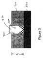
図3を参照して、ART構造は、次のステップに従って形成することができる。半導体基板300、即ち半導体ウェハが提供される。半導体基板300は、半導体材料を含むことができ、例えばバルクシリコンウェハ、またはバルクゲルマニウムウェハとすることができる。基板300は、例えば、第IV族元素(例えば、ゲルマニウムまたはシリコン)のような第1半導体材料を含む、または実質的にそれから構成することができる。一実施例では、基板100は、(300)シリコンを含む、または実質的にそれから構成される。 Referring to FIG. 3, the ART structure can be formed according to the following steps. A
誘電材料を含む誘電体層310、即ち、例えばSiO2などの非晶質材料が半導体基板300上に形成される。SiO2は、誘電材料の1つの例だけで、当業者は、例えばSiNxなど適当に再結合の影響を低減する他の材料に置き換えることもできる。誘電体層310は、例えば熱酸化またはプラズマ化学気相成長法(PECVD)などの当業者に周知の方法によって、例えばSanta Clara, CAを本拠地にしているApplied Materialによって製造されたCENTURA ULTIMAなどの適当なシステムで形成することができる。誘電材料は、結晶質材料が誘電体層に穿通して形成された開口に堆積されるのに必要な高さに対応した厚さt1を有することができる。いくつかの実施例では、誘電体層310の厚さt1は、例えば25nm〜20μmの間を上下することができる。A
複数の狭いサブミクロン幅の開口、例えばトレンチ320は、従来のリソグラフィーと反応性イオンエッチングによって誘電体層310に定められ、この開口は誘電側壁325を有する。当業者は又、トレンチの側壁を不活性化するため、例えば水素プラズマを用いたSiO2処理などの各種アプリケーションに対してプロセスを適合する追加ステップをどのように行うかは分かる。A plurality of narrow sub-micron wide openings, such as
洗浄後、格子不整合材料330は、開口320内で選択的に成長する。格子不整合材料は、III−V族半導体またはゲルマニウムであることができ、例えば、選択エピタキシャルによって開口に成長される。格子不整合材料の貫通転位は、通常、開口の側壁に向いて傾斜し、例えばSiO2の誘電材料に届いた時、終了する。よって、トレンチの上部付近のエピタキシャル材料の領域は、実質的に転位が含まれないことが望ましい。After cleaning, the
ART構造は、以下に論ぜられるように太陽電池の欠陥捕獲(defect-trapping)層として用いることができる。ART構造は、(i)結晶質材料と隣接の半導体材料間の格子不整合から生じる欠陥を含む結晶質材料と(ii)非結晶質材料で終了する欠陥の非結晶質材料を含む。 The ART structure can be used as a defect-trapping layer for solar cells as discussed below. The ART structure includes (i) a crystalline material containing defects resulting from lattice mismatch between the crystalline material and an adjacent semiconductor material, and (ii) an amorphous material with defects ending with an amorphous material.
例えばゲルマニウムをSiO2側壁間のトレンチに堆積する時、ゲルマニウム原子と酸素原子間の結合は、2つのゲルマニウム原子間の結合より高いエネルギーを必要とする。よって、Ge-O結合はあまり好都合ではないため、あまり形成されそうもない。よって、典型的な成長条件下では、図4に示すようにゲルマニウム原子は、ファセット400、一般的に{111}または{113}の結晶面を形成する。For example, when germanium is deposited in a trench between SiO2 sidewalls, the bond between germanium and oxygen atoms requires higher energy than the bond between two germanium atoms. Thus, Ge—O bonds are not very convenient and are not likely to be formed. Thus, under typical growth conditions, germanium atoms form
2つの誘電体層の側壁間では、2つの結晶面、例えば{111}面500と{100}面500’は、同時に形成することができる。2つの面の成長率(レート)は、異なってもよい。例えば、図5に示されるように、ゲルマニウムでは、{100}面は{111}面より早く成長する。また図5に示されるように、早い(ファースト)成長面の方向の結晶成長は、遅い(スロー)成長面の成長率によって制限されるので、最終的に早い成長面は消失する。 Between the side walls of the two dielectric layers, two crystal planes, for example, {111}
これらの2つの結晶方向の観測を可能にするために、マーカー(marker)層600を定めるマーカー材料の薄膜領域が格子不整合材料330間に挟設することができる。例えば、薄膜Si-Ge領域、または“マーカー層”は、ゲルマニウムマトリクス内に挟設され、TEM像のコントラストを提供することができる。これらのマーカー層600は、図6のTEM顕微鏡写真の略図に黒山形(chevron)で表示されている。ゲルマニウムは、図(文字Aの下方)の最下部分で{100}結晶方向に成長される。その領域の上方では、角度のあるSi-Geマーカー層は、ゲルマニウムが{111}成長面またはファセットに遷移されるのを示している。貫通転位610の下記の挙動が観測される。
基板300から{100}結晶方位を具備した領域500’を穿通し、文字Aに向いて垂直に成長する
Aの位置では、貫通転位は、{111}結晶方位領域500に交差する。結晶のファセットは、貫通転位を{111}ファセットと垂直の方向に向け、側壁の方に向く。
貫通転位は、SiO2の側壁に到達し、終了する。In order to allow observation of these two crystal directions, a thin film region of marker material defining the marker layer 600 can be sandwiched between the lattice mismatched
A
At the position A, threading dislocations intersect the {111}
The threading dislocation reaches the SiO2 sidewall and ends.
貫通転位がファセットの境界線に届いた時、結晶境界は、通常ファセットに垂直な方向にそれを再度向ける。ファセットは、側壁に向いて貫通転位を傾斜する。材料の全ての貫通転位は、下方の基板に平行しないファセットを有するため、側壁が十分高い時、通常側壁に交差する。いくつかの実施例では、トレンチのアスペクト比、即ち縦横比は、約1より大きいことが好ましい。側壁は、好ましくは転位を捕獲し、トレンチの上部にエピタキシャル材料の欠陥のない領域を残す。このアプローチは、1つのリソグラフィーと1つの選択エピタキシャル成長ステップで基板のインターフェース欠陥を実質的に除去する。 When the threading dislocation reaches the facet boundary, the crystal boundary redirects it normally in a direction perpendicular to the facet. The facet slopes threading dislocations towards the side wall. All threading dislocations of material have facets that are not parallel to the underlying substrate, so when the sidewalls are sufficiently high, they usually intersect the sidewalls. In some embodiments, it is preferred that the trench aspect ratio, or aspect ratio, be greater than about one. The sidewalls preferably capture dislocations and leave a defect-free region of epitaxial material at the top of the trench. This approach substantially removes substrate interface defects with one lithography and one selective epitaxial growth step.
ARTサンプルは、ゲルマニウムとヒ化ガリウム(GaAs)を用いて作成される。ゲルマニウムは、シリコン基板上のSiO2トレンチ内に堆積される。サンプルの薄膜のTEM像は、SiO2側壁が全ての貫通転位を捕獲し、トレンチの上部に欠陥のないゲルマニウムを残すことを示した。図7を参照して、TEM像の概略図は、例えば200nm幅のトレンチの開口320に堆積されたゲルマニウムは、捕獲領域の上方は欠陥610は無くすことができることを示している。材料の上面図(“平面図”)のTEM像が捕らえられた。図8に示されるように、TEM像に基づいた概略図は、SiO2側壁325による貫通転位の捕獲を示しており、転位がART領域の底部の側壁で終了している。ART samples are made using germanium and gallium arsenide (GaAs). Germanium is deposited in the SiO2 trench on the silicon substrate. A TEM image of the sample thin film showed that the SiO2 sidewall captures all threading dislocations, leaving a defect-free germanium on top of the trench. Referring to FIG. 7, the schematic view of the TEM image shows that, for example, germanium deposited in the
図9を参照して、転位を含むゲルマニウムの下部領域は、除去することができる。基板300と転位610領域の除去後、上部領域は、欠陥は無くすことができる。上部領域のゲルマニウムは、格子不整合による無穿通転位、無堆積欠陥、無双晶(2次元的格子欠陥)と、無亀裂を含有することができる。 Referring to FIG. 9, the lower region of germanium containing dislocations can be removed. After removal of the
図10は、例えばシリコンなどの基板300上の誘電体の側壁(例えばSiO2)間に、結晶質材料(例えばGaAs)で充填されたトレンチを示している。貫通転位610は、トレンチの底部付近の側壁325に向いて傾斜する。GaAsは、点線以上の領域に欠陥がない。ARTの使用により、シリコン基板上に高品質のIII−V族材料の堆積は立証されており、これによりシリコン基板上に高効率、低コストの多接合太陽電池を形成する実現性を裏付けることができる。FIG. 10 shows a trench filled with a crystalline material (eg GaAs) between dielectric sidewalls (eg SiO2 ) on a
分析により、熱膨張係数の不整合は、ARTを用いて格子不整合材料を成長する時、通常亀裂は生じないことが証明された。亀裂の不存在は、下記のうちの1つ以上によるものである:
エピタキシャル層は薄いので、応力は小さい。
非常に広いトレンチと対比して、トレンチは比較的狭いので熱膨張係数の不整合から生じる応力を弾性的に緩和することができ、材料反応(behavior)はバルク膜(bulk film)に近似する。
例えばSiO2などの側壁の誘電材料は、半導体材料よりも適合性が高い傾向があり、膨張接点となって応力を暖和するように伸びることができる。Analysis has shown that thermal expansion coefficient mismatches usually do not crack when growing lattice mismatched materials using ART. The absence of cracks is due to one or more of the following:
Since the epitaxial layer is thin, the stress is small.
In contrast to very wide trenches, the trenches are relatively narrow so that stresses resulting from thermal expansion coefficient mismatch can be elastically relaxed, and the material behavior approximates a bulk film.
For example, dielectric materials on the sidewalls such as SiO2 tend to be more compatible than semiconductor materials and can be expanded contacts to warm up stresses.
図2を再度参照して、In0.5Ga0.5 P (1.86 eV)、Si (1.15 eV)と、In0.7Ga0.3As (0.61 eV)から作られた3接合太陽電池の実施例の格子とバンドギャップのパラメータが示されている。太陽電池は、63.2%の理論的最大効率を有する。この図は、50%のインジウムと50%のガリウムを有するInGaP材料を用いた素子(device)が示されているが、他の濃度のインジウムとガリウムが用いられて材料のバンドギャップと格子定数を調整し、太陽電池の性能を改善することができることを示している。同じことがInGaAs層にも当てはまり、70%のインジウムと30%のガリウムのバンドギャップが示されているが、他の比率のインジウムとガリウムがInGaAs層に用いられて、性能改善のためバンドギャップと格子定数を調整することができる。例えば、以下に述べるように、InPに格子整合したInGaAs層を用いることが望ましく、この場合、In0.53Ga0.47Asを用いることができる。Referring back to FIG. 2, the lattice and band gap of an example of a three-junction solar cell made from In0.5 Ga0.5 P (1.86 eV), Si (1.15 eV), and In0.7 Ga0.3 As (0.61 eV). The parameters are shown. The solar cell has a theoretical maximum efficiency of 63.2%. The figure shows a device using an InGaP material with 50% indium and 50% gallium, but other concentrations of indium and gallium are used to determine the bandgap and lattice constant of the material. It shows that it can be adjusted to improve the performance of solar cells. The same applies to the InGaAs layer, which shows a band gap of 70% indium and 30% gallium, but other ratios of indium and gallium are used in the InGaAs layer to improve the band gap and improve performance. The lattice constant can be adjusted. For example, as described below, it is desirable to use an InGaAs layer lattice-matched to InP. In this case, In0.53 Ga0.47 As can be used.
図11は、ARTによって、シリコン基板300の上部に形成されたp-n接合を有するInGaP領域を含む上部ART領域1110、シリコン基板内のp-n接合1120と、ARTによってシリコン基板の底部表面に定められたp-n接合を有するInGaAs領域を含む底部ART領域1130を含む3接合太陽電池構造1100を示している。上述の構造は、トンネル接合を組み込み、3つのサブセル、即ち、上部ART領域、基板と、底部ART領域間の電気的コンタクトを作る。 FIG. 11 shows an
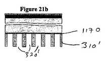
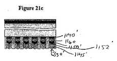
特に、上部ART領域1110は、第1非結晶質材料310(例えば、SiO2)に近接して接触している第1結晶質材料330(例えば、InGaP)を含む第1欠陥捕獲層として機能を果たすことができる。第1結晶質材料は、第1結晶質材料の格子不整合と第1隣接材料(例えばシリコン基板300)間に生じた欠陥610を含み、この欠陥は第1非結晶質材料310で終了する。上部ART領域1110は、例えばp+型GaAsの湿潤層1140を含むことができる。湿潤層1140の構成は、第1結晶質材料(例えばInGaP)の連続成長を可能にするため、下方の材料(例えばシリコン)上に高品質かつ連続する層を形成するように選択される。上部ART領域は、例えばp型InGaPのベース1145と、例えばn+型InGaPのエミッタ1150を含むこともできる。InGaPは、適当なバンドギャップを有するので、選択することができる。光起電性接合1152は、ベース1145とエミッタ1150間のインターフェースによって定められる。InGaP材料とInとGaの比率は、材料が約1.86eVのバンドギャップを有するように選択される。このバンドギャップは、上部サブセルが高エネルギー光子を効率よく吸収するが、低エネルギー光子が障害なく通過することが可能なように選択される。エミッタは、高ドープされたn型であり、InGaPと上部接触金属間の低抵抗を提供する。ベースは、InGaPが少数キャリア寿命を有するように低ドープされたp型であり、電子−孔子ペアがp-n接合によって分離される前に電子−孔子ペアが再結合しないように選ばれる。上部ART領域は、例えば約1〜5μmの厚さを有することができる。例えばNiAuなどの導電材料の上部接触層1155は、上部ART領域をおおって配置することができる。In particular, the
底部ART領域1130は、第1欠陥捕獲層の下に配置された第2欠陥捕獲層として機能することができ、この第2欠陥捕獲層は、第2非結晶質材料310’(例えば、SiO2)に隣接して接触している第2結晶質材料330’(例えば、InGaP)を含む。第2結晶質材料は、格子不整合と第2隣接材料(例えばシリコン基板)間に生じる欠陥610’を含み、この欠陥は第2非結晶質材料310’で終了する。底部ART領域1130は、例えばn+型GaAsの湿潤層1140’、例えばn+型InPの底部捕獲領域1160、例えばn+型InGaAsのエミッタ1150’と、p型InGaAsのベース1145’を含むことができ、光起電性接合1152’は、例えばn+型InGaAsのエミッタ1150’と例えばp型InGaAsのベース1145’間のインターフェースによって定められる。底部ART領域1130は、例えば約1〜5μmの厚さを有することができる。例えばNiAuなどの例えば導電材料の底部接触層1155’は、底部ART領域上に配置することができる。The
太陽電池、即ち、p-n接合1120は、例えばシリコン基板の上部および底部欠陥捕獲層間に配置され、n+とp+ドーピングを用いて定めることができる。p-n接合は、例えばイオン注入によってp型Siの基板に形成された、例えばn+型Siのエミッタ1167によって定めることができ、基板の残りの部分はベース1168を定め、p-n接合1120は、エミッタとベース間に配置されている。A solar cell, or pn junction 1120, is disposed, for example, between the top and bottom defect trapping layers of the silicon substrate and can be defined using n+ and p+ doping. The pn junction can be defined by, for example, an n+ -
トンネル接合1170は、基板300と上部ART領域間に形成されることができ、他のトンネル接合1170’は、基板と底部ART領域間に形成することができる。トンネル接合は、非常に高ドープのp+/n+ダイオードである。ドーピングは、電流をp+とn+層間を通り抜ける(トンネルする)のに十分高く、トンネル接合は、2つの隣接層間の低抵抗接触を形成する。言い換えれば、上部ART領域が光にさらされた時、ドーピングは、p+/n+接合の空乏領域がトンネルを生じるように十分に小さくなり、電流が上部ART領域に流れるように十分に高い。電流は、トンネル接合をフォワードバイアスする。トンネル接合は、半導体基板300の上方と下方に形成されたIII−V族材料に形成することができる。成長中の現場(in-situ)ドーピングによってこのような層の高濃度、例えば約1×1019/cm3より上のp+とn+ドーピングが得ることができる。好適なトンネル接合は、空乏領域の厚さが約10nmであるように選択することができる。例示されるように、実施例では、トンネル接合1170、1170’は、シリコン基板300の上部と底部に定めることができる。次に、シリコン基板の上部から始まるシリコンのドーピングは、以下の通りである:
p++ (トンネル接合) 1170
n++ (トンネル接合) 1170
n+ (エミッタ) 1167
p (ベース) 1168
p++(トンネル接合) 1170'
n++(トンネル接合) 1170'A
p ++ (tunnel junction) 1170
n ++ (tunnel junction) 1170
n + (emitter) 1167
p (base) 1168
p ++ (tunnel junction) 1170 '
n ++ (tunnel junction) 1170 '
構造は、例えば、第2欠陥捕獲層の下方、または第1欠陥捕獲層の上方に配置された追加の太陽電池を含むことができる。いくつかの実施例では、第1と第2欠陥捕獲層の双方が、基板の上方に配置される。 The structure can include, for example, an additional solar cell disposed below the second defect capture layer or above the first defect capture layer. In some embodiments, both the first and second defect capture layers are disposed above the substrate.
各種の実施例では、300nm〜500nm幅のトレンチの大きなアレイ(〜500,000が12インチの基板にある)がシリコン基板上の各ダイの表面を覆う。他の実施例では、トレンチ幅は、例えば180nm〜5μmのより広い範囲で変化することができる。トレンチ間の距離は、太陽放射のほぼ全ての波長以下である。この構成は、太陽放射がトレンチ間を通過するのから防ぐことができる。よって、太陽電池は、ほぼ全ての入射光を吸収することができる。〜150nmの間隔は、一部の基準には好ましいが、間隔は、必要なアプリケーションと、または材料に基づいて実質的に調整することができる。 In various embodiments, a large array of 300 nm to 500 nm wide trenches (˜500,000 on a 12 inch substrate) cover the surface of each die on the silicon substrate. In other embodiments, the trench width can vary over a wider range, for example from 180 nm to 5 μm. The distance between the trenches is below almost all wavelengths of solar radiation. This configuration can prevent solar radiation from passing between the trenches. Therefore, the solar cell can absorb almost all incident light. A spacing of ˜150 nm is preferred for some criteria, but the spacing can be substantially adjusted based on the required application or material.
図11に示されたARTベースの3接合太陽電池構造は、以下のように動作する:
まず、太陽光が上部ART太陽電池1110のInGaP材料330を照射する。InGaPは、1.82eV以上の高いエネルギーの光子を吸収する。1.82eVより低いエネルギーの光子は、InGaPを通過し、シリコン基板300に入射する。
InGaPを通過した光子は、上部欠陥捕獲層1165に入射する。この領域の吸収は、光生成キャリアが貫通転位610で再結合する可能性があるため、回避、または低下することが好ましい。ほとんどの上部捕獲領域は、InGaPから作られるため、上述のInGaPの領域によって吸収されない光子に対して透明である。GaAsの湿潤層1140がシリコン上にInGaPの2次元成長を促進するように提供されている間、この層は、シリコンに通過する光子の吸収を低下するように非常に薄く保持される。当業者は、湿潤層により吸収を減少するため他の材料を適用することが理解されよう。
シリコンは、1.15eV以上の高いエネルギーの光子を吸収する。1.15eVより低いエネルギーの光子はシリコン基板300を通過する。
シリコンを通過した光子は、第2捕獲領域、即ち、底部捕獲領域1160を通過する。再度、この目標は、光生成されたキャリアが貫通転位で再結合する可能性があるため、この領域での吸収を回避することである。よって、捕獲領域は、高バンドギャップの材料のInPから作られることが好ましい。低エネルギー(≦1.15eV)の光子はInP捕獲領域を通過してInGaAs領域に入る。InPは、シリコン上に非平面モード(mode)で成長するため、薄層GaAs湿潤層は、シリコン上に形成され、InPの2次元層を形成することが好ましい。GaAsは、広いバンドギャップを有するため、この領域の低エネルギー光子を吸収しない。
次に、InGaAsは、0.61eV以上の高いエネルギーの光子を吸収し、InGaAsのp-n接合が光生成の電子−孔子ペアを分離する。The ART-based three-junction solar cell structure shown in FIG. 11 operates as follows:
First, sunlight irradiates the
Photons that have passed through InGaP are incident on the upper defect trapping layer 1165. Absorption in this region is preferably avoided or reduced because photogenerated carriers may recombine at threading
Silicon absorbs high energy photons of 1.15 eV and above. Photons with energy lower than 1.15 eV pass through the
Photons that have passed through the silicon pass through the second capture region, ie, the
Next, InGaAs absorbs high energy photons of 0.61 eV or higher, and the InGaAs pn junction separates the photogenerated electron-hole pairs.
上述のように、光はART太陽電池の捕獲領域を通過する。転位は、サブバンドギャップの光子を吸収する可能性があるが、このサブバンドギャップの吸収は、ARTベースセルの性能に大きく影響しない。 As mentioned above, the light passes through the capture area of the ART solar cell. Dislocations can absorb subbandgap photons, but this subbandgap absorption does not significantly affect the performance of the ART base cell.
捕獲領域では、貫通転位は、バンドギャップ内に電子状態を作る。よって材料は、捕獲領域を通過するサブバンドギャップの光子を数パーセント吸収する。光生成キャリアは貫通転位付近に現れることから、非放射で、即ち、太陽電池の出力電力に貢献することなく、再結合する傾向がある。吸収係数αと厚さtの関数の透過率Tを提供する以下の公式でこの損失機構の影響を推定することが可能である:
T =e-αtIn the trapping region, threading dislocations create an electronic state in the band gap. Thus, the material absorbs several percent of the subband gap photons that pass through the capture region. Since photogenerated carriers appear in the vicinity of threading dislocations, they tend to recombine non-radiatively, that is, without contributing to the output power of the solar cell. It is possible to estimate the effect of this loss mechanism with the following formula that provides a transmittance T as a function of the absorption coefficient α and the thickness t:
T = e-α t
シリコン上に成長したInPとGaAs領域の吸収係数は、バンドギャップより下の0と0.5eV間のエネルギーの光子に対して約5×10³/cmであることが伝えられている。高転位領域の厚さは、約100nmであり、ARTトレンチは通常500nm以下のオーダーの幅を有するのが通常となりうる装置は、捕獲領域を介する透過率は、約95%と見込まれる。It is reported that the absorption coefficient of the InP and GaAs regions grown on silicon is about 5 × 10³ / cm for photons with energy between 0 and 0.5 eV below the band gap. The thickness of the high dislocation region is about 100 nm and the device where the ART trench can typically have a width on the order of 500 nm or less is expected to have a transmission through the capture region of about 95%.
ここに記述された3接合太陽電池の効率に対する上述の現象の影響を推定することは可能である。InGaPは、光子が捕獲領域に入る前に、光子の約33%を吸収する。光子の残りの67%は、InGaPセルの捕獲領域に入る。InGaPセルの捕獲領域は、その67%のうちの約5%、または太陽電池に入射した全ての光子の約3.3%を名目上吸収する。 It is possible to estimate the effect of the above phenomenon on the efficiency of the three-junction solar cell described here. InGaP absorbs about 33% of the photons before they enter the capture region. The remaining 67% of the photons enter the capture region of the InGaP cell. The capture region of the InGaP cell nominally absorbs about 5% of its 67%, or about 3.3% of all photons incident on the solar cell.
次に、残りの光子は、InGaAsセルの捕獲領域に入る前にシリコンセルに通過する。この時までに、2つの上部(InGaPとシリコン)セルは、太陽電池に入射した全ての光子の約67%を吸収している。太陽電池に入射した全ての光子の約33%だけがInGaAsセルの捕獲領域に到達する。捕獲領域は、その33%のうちの約5%、または太陽電池に入射した全ての光子の約1.7%を名目上吸収する。 The remaining photons then pass through the silicon cell before entering the capture region of the InGaAs cell. By this time, the two upper (InGaP and silicon) cells have absorbed about 67% of all photons incident on the solar cell. Only about 33% of all photons incident on the solar cell reach the capture region of the InGaAs cell. The capture region nominally absorbs about 5% of that 33%, or about 1.7% of all photons incident on the solar cell.
次に、総計で、捕獲領域は、入射した全ての光子の〜3.3%+〜1.7%=〜5%吸収する。これらの簡単な計算は、貫通転位付近のサブバンドギャップ領域の光子吸収量が小さい損失機構であることを示し、これにより、ART太陽電池が63%の最大理論効率を達成することから防げられる可能性があるが、50%を超える生産効率を妨げることはない。 Then, in total, the capture region absorbs ~ 3.3% + ~ 1.7% = ~ 5% of all incident photons. These simple calculations show a loss mechanism with low photon absorption in the subband gap region near threading dislocations, which can prevent ART solar cells from achieving a maximum theoretical efficiency of 63% But does not hinder production efficiency above 50%.
太陽電池におけるARTの利用により、転位の不利な影響を減少することができる。バルク材料では、転位は、例えば約10μmまでの比較的長い距離に対して再結合を誘起することができる。300〜500nm幅のトレンチの太陽電池を作るためのARTの利用により、転位は隣接するトレンチの再結合を誘起することができないので、バルク材料または薄膜における欠陥の影響に比べ、欠陥の影響領域を大きく減少する。 The use of ART in solar cells can reduce the adverse effects of dislocations. In bulk materials, dislocations can induce recombination for relatively long distances, for example up to about 10 μm. By using ART to create 300-500 nm wide trench solar cells, dislocations cannot induce recombination of adjacent trenches, thus reducing the effect area of defects compared to the effect of defects in bulk materials or thin films. Decrease significantly.
ARTを用いてシリコン上にInGaPとInGaAsを形成することは、図11に示された3接合セルを形成するのに用いられる製造プロセスの重要な部分である。ARTを用いてシリコン上にInGaPとInGaAsを形成する技術をより詳細に述べる。 Forming InGaP and InGaAs on silicon using ART is an important part of the manufacturing process used to form the three-junction cell shown in FIG. The technique of forming InGaP and InGaAs on silicon using ART will be described in more detail.
図12は、InGaPを成長させるART構造の実施例を示している。適当なシリコン基板300は、例えばSEMATECHの子会社ATDFから入手することができる。例として、p型シリコン(001)基板は、6°でオフカットされ、逆位相領域境界を回避する。例えば熱酸化物の1〜1.5μmの厚さを有する比較的厚い誘電体層310は、基板上に形成される。例えば0.2〜2.5μmの幅を有するトレンチ320は、フォトリソグラフィーとドライエッチングによって熱酸化物にパターン化される。 FIG. 12 shows an example of an ART structure for growing InGaP. A
パターン化ステップ後、カーボン残留物は、酸素プラズマ灰化ステップ(酸素プラズマ灰化装置で800W、1.2トール(Torr)、30分間の条件下で処理)によって、基板表面から除去することができる。残留物の除去は、例えば、Fremont,CAを本拠地にしているMattson Technology, Inc. によって製造されたASPEN STRIPIIシステムで実行することができる。パターン化された基板は、例えば、Piranha溶液、SC2溶液と、低濃度フッ酸(HF) 溶液で順次に清浄される。エピタキシャル格子不整合材料330は、例えば有機金属気相成長(MOCVD)によってトレンチに選択的に形成される。エピタキシャル格子不整合材料330は、GaAsの湿潤層1140上に配置されたInGaPを含むことができる。 After the patterning step, the carbon residue can be removed from the substrate surface by an oxygen plasma ashing step (800 W, 1.2 Torr, processed for 30 minutes in an oxygen plasma ashing apparatus). . Residue removal can be performed, for example, on an ASPEN STRIPII system manufactured by Mattson Technology, Inc., based in Fremont, CA. The patterned substrate is sequentially cleaned with, for example, a Piranha solution, an SC2 solution, and a low concentration hydrofluoric acid (HF) solution. The epitaxial
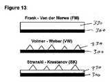
図13は、格子不整合材料330の3つの可能な成長モードを示している。Frank-Van der Merwe (FM) モードでは、材料330は、2次元で一層ずつ基板上に成長する。Volmer-Weber (VW)モードでは、界面エネルギーは、エピタキシャル材料330の孤立(isolated)パッチを形成し、成長して合体(coalesce)する。Stranski-Krastanov (SK)モードでは、材料330は、臨界膜厚に達成するまで一層ずつ成長してから、パッチで成長する。 FIG. 13 shows three possible growth modes of the lattice mismatched
InGaPは、非平面モード、即ち、第2(VW)か、第3(SK)モードのいずれかでシリコン上に成長する傾向がある。非平面成長(即ち、VWまたはSKモード)は、一般的に高濃度の欠陥と粗面を招く。いくつかの実施例では、この問題は、例えばGaAsの湿潤層1140をInGaPに堆積する前に、シリコン基板上に直接堆積することで対応できる。GaAsは、シリコン上に2D層で成長し、InGaPは、GaAs上に2D層で成長する。表2は、GaAs とInGaPを成長させるように調整されることができる条件の模範的なセットを示している。
V/III元素比は、V族前駆体中のV族元素の流量とIII族前駆体中のIII族元素の流量間の比率として定められており、(V族前駆体流量/III族前駆体流量)*(V族前駆体中のV族元素の比率/III族前駆体中のIII族元素の比率)で算出される。要約すれば、V−III族の比率は、処理チャンバに入るV族原子/秒の数を処理チャンバに入るIII族原子/秒の数で割ったのと等しい。The V / III element ratio is determined as a ratio between the flow rate of the Group V element in the Group V precursor and the flow rate of the Group III element in the Group III precursor, and is expressed as (Group V precursor flow rate / Group III precursor). (Flow rate)* (ratio of group V element in group V precursor / ratio of group III element in group III precursor) In summary, the group V-III ratio is equal to the number of group V atoms / second entering the processing chamber divided by the number of group III atoms / second entering the processing chamber.
成長条件は、さまざまな方法で調整することができる。例えば:
例えば800℃〜1000℃の温度範囲で基板をプレエピタキシーベーキング(pre-epitaxy bake)する。
成長中、室内温度から800℃の温度で熱サイクルアニールする。
例えばInGaP、Si、SiO2などの異なる材料間の熱膨張係数の不整合の結果として堆積欠陥の可能性を軽減し、1つ以上の材料を処理してその熱膨張性質を変える、例えば、SiO2を熱窒化処理(thermal nitrogen treatment)に付して、その熱膨張係数をシリコンに近づける。Growth conditions can be adjusted in various ways. For example:
For example, the substrate is pre-epitaxy bake in a temperature range of 800 ° C. to 1000 ° C.
During the growth, thermal cycle annealing is performed at a temperature from room temperature to 800 ° C.
For example InGaP, Si, reduce the possibility of stacking faults as a result of the mismatch in thermal expansion coefficients between different materials, such as SiO2, it changes its thermal expansion properties and processing one or more materials, eg, SiO2 is subjected to thermal nitrogen treatment to bring its thermal expansion coefficient closer to that of silicon.
図11に示された3接合太陽電池構造などのいくつかの実施例では、高バンドギャップのInP捕獲領域は、シリコン基板とInGaAs間に挟設され、最下層の太陽電池の捕獲領域の光子吸収を回避することができる。捕獲領域のバンドギャップは、捕獲領域下方のサブセルのバンドギャップより大幅に高いことが好ましい。光子が捕獲領域で吸収された場合、吸収された光子は、捕獲領域の転位で再結合するため、電気エネルギーに変換しない。捕獲領域のバンドギャップが大きい場合、光子は、捕獲領域を通過し易く、下方にあるサブセルによって効果的に吸収される。 In some embodiments, such as the three-junction solar cell structure shown in FIG. 11, the high bandgap InP trapping region is sandwiched between the silicon substrate and InGaAs, and the photon absorption in the trapping region of the lowermost solar cell. Can be avoided. The band gap of the capture region is preferably significantly higher than the band gap of the subcell below the capture region. When photons are absorbed in the capture region, the absorbed photons do not convert to electrical energy because they recombine at the capture region dislocations. If the trap region has a large bandgap, photons are likely to pass through the capture region and are effectively absorbed by the underlying subcell.
上述の考察において、InGaAsは、InPとほぼ格子整合するので、InPが他の高バンドギャップ材料よりもむしろ挟設されるよりも適するが、当業者は、どのように他の適合する材料を用いるかはわかるだろう。 In the above discussion, InGaAs is nearly lattice matched to InP, so InP is more suitable than sandwiched rather than other high bandgap materials, but those skilled in the art will know how to use other compatible materials. You will know if it is.
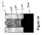
図14は、例えば広バンドギャップInPの第1結晶質材料330がトレンチ320に配置されたGaAs湿潤層1140上に形成された構造を示している。続いて、例えばInGaAsのもう1つの結晶質材料1400が例えばInPの第1結晶質材料上に形成される。InPは、欠陥を捕獲するように用いられ、大きいバンドギャップを有するため、光がそれに吸収されない。InGaAsは、太陽電池として機能する。表3は、InPとInGaAsを成長するように調整することができる条件の模範的なセットを示している。
図15は、単一接合InGaP太陽電池1500の模範的な構造を表している。注意するのは、図15とここでの太陽電池の他の図は、正確な図というよりむしろ、概略図である。これらは例えば、接触(contact)ドーピング領域、窓層と、裏面電界を省略しているが、その存在は当業者には容易にわかるであろう。 FIG. 15 illustrates an exemplary structure of a single junction InGaP
単一接合太陽電池1500は、図11を参照して述べられたように、上部ART領域1110と、p+型Siの基板300上のトレンチ320に配置されるp+型GaAsの湿潤層1140を含む。InGaPのベース層1145は、湿潤層1140上に配置され、n+型InGaPのエミッタ層1150は、ベース層上に配置され、その間に光起電性接合1152を定める。上部ART領域は、例えば約1〜5μmの厚さを有することができる。例えばNiAuなどの導電材料の上部接触層1155は、上部ART領域上に配置することができる。例えばアルミニウム層の底部接触層1155’は、上部ART領域の反対側のシリコン基板側に形成することができる。上部および底部接触層の金属層は、隣接の半導体材料により低接触抵抗を提供するよう選択されることが好ましい。例えば、アルミニウムは、III−V材料でなくドープされたシリコンで低接触抵抗を提供する。よって、アルミニウムは、ドープされたシリコンに隣接する接触層として用いられることが好ましい。シリコン基板300は、p+型でドープされ、約200〜700μmの厚さを有し、好ましくは、約300μmの厚さを有する。太陽光は、上部接触層1155を経由して単一接合太陽電池1500を照射することができる。The single-junction
トレンチ幅、層厚と、ドーピングレベルは、効率を増すために変えることができる。いくつかの実施例では、InGaPの厚さは、約1〜1.5μmの間である。当業者は、特定のアプリケーションの実験を実施しなくともどのように素子の幾何学的構造、ドーピングレベルと、材料係数を調整するかがわかるであろう。 The trench width, layer thickness, and doping level can be varied to increase efficiency. In some embodiments, the thickness of InGaP is between about 1 and 1.5 μm. Those skilled in the art will know how to adjust device geometry, doping levels, and material coefficients without having to experiment with specific applications.
図16は、単一接合InGaAs太陽電池1600の構造を示している。InGaP太陽電池と同じように、トレンチ幅、層厚と、ドーピングレベルは、効率を増すために合わせることができる。 FIG. 16 shows the structure of a single junction InGaAs
単一接合InGaAs太陽電池1600は、図11を参照して述べられたように、n+型Siの基板300上に形成された底部ART領域1130を含む。底部ART領域1130は、例えばn+型GaAsの湿潤層1140’、例えばn+型InPの底部捕獲領域1160、例えばn+型InGaAsのエミッタ1150’と、p型InGaAsのベース1145’を含むことができ、光起電性接合1152’は、エミッタ1150’とベース1145’間のインターフェースによって定められる。底部ART領域1130は、例えば約1〜5μmの厚さを有することができる。例えばNiAuなどの例えば導電材料の底部接触層1155’は、底部ART領域上に配置することができる。例えばアルミニウム層の上部接触層1155は、底部ART領域の反対側のシリコン基板側に形成することができる。太陽光は、上部接触層1155を経由して単一接合太陽電池1500を照射することができる。Single-junction InGaAs
いくつかの実施例では、InGaAsの厚さは、約1〜3μmの間にある。底部ART領域1130は、1〜5μmの厚さを有することができる。基板は、約300μmの厚さを有することができる。当業者は、どのように素子の幾何学的構造、ドーピングレベルと、材料係数を調整して、特定のアプリケーションの素子性能を最適化するかがわかるであろう。 In some embodiments, the InGaAs thickness is between about 1 to 3 μm. The
図17は、2接合InGaP/Si太陽電池1700の実施例を示しており、図18は、InGaAs/Si太陽電池1800の実施例を示している。2接合InGaP/Si太陽電池1700は、図11を参照して述べられたように、上部ART領域1110を含み、第1光起電性接合1152を有し、基板上に配置されて第2接合を定める。特に、基板は、p型シリコンとし、約300μmの厚さを有することができる。n+型Siのエミッタ領域1705は、イオン注入によって基板300内に形成されることができる。ベース1710は、基板300の残りによって定めることができる。よって、第2光起電性接合1720は、エミッタ1705とベース1710の間に形成される。トンネル接合1170は、上部ART領域1110とエミッタ1705の間に配置することができる。例えば、アルミニウムの底部金属層1155’は、基板300の背面上に形成される。上部ART領域1110は、エミッタ1705に隣接して形成することができる。FIG. 17 shows an example of a two-junction InGaP / Si
図18の2接合太陽電池1800は、第1格子定数と第1バンドギャップエネルギーを有する、例えばシリコンの第1半導体材料を含む第1光起電性電池を含み、第1光起電性電池は、シリコン基板300に対応し、n+型Siのエミッタ1705、p型Siのベース1710と、光起電性接合1720を含む。第2光起電性電池は、第1格子定数と異なる第2格子定数と第1バンドギャップエネルギーより低い第2バンドギャップエネルギーを有する第2半導体材料を含む。第2光起電性電池は、図11を参照して述べられたように、底部ART領域1130の例えばInGaAsのベース1710に隣接して形成することができる。特に、第2光起電性電池は、n+型InGaAsのエミッタ1150’と、p型InGaAsのベース1145’を含むことができ、光起電性接合1152’は、エミッタとベース間のインターフェースに形成される。The two-junction solar cell 1800 of FIG. 18 includes a first photovoltaic cell having a first lattice constant and a first bandgap energy, for example including a first semiconductor material of silicon, the first photovoltaic cell being , Corresponding to the
欠陥捕獲層1160は、第1と第2光起電性電池間に配置される。欠陥捕獲層は、第2バンドギャップエネルギーより高い第3バンドギャップエネルギーを有する例えばn+型InPの材料を含む。欠陥捕獲層1160は、非結晶質材料310(例えばSiO2)に近接した結晶質材料(例えばInP)を含み、結晶質材料は、非結晶質材料で終了した欠陥を含む。A
図15と図16に示された構造の代案では、太陽電池構造がトレンチからあふれ出るまで成長する膜を含み、図19に示されたようにART緩衝層1900を形成することができる。例示された実施例は、ART緩衝層1900を組み込んだ単一接合ART太陽電池1905を示している。隣接の不連続領域の格子不整合材料は、単一連続膜、即ちART緩衝層1900を形成するように合体(coalesce)される。次に、太陽電池のp-n接合は、緩衝層上に形成される。太陽電池のp-n接合は、ベース1910とエミッタ1920を含み、金属1930をその上に配置することができる。エミッタ、ベースと、誘電体層の総厚は、約1〜5μmとすることができる。上述の構造は、例えばシリコンの基板300上に形成され、約300μmの厚さを有することができる。図19の具体例に示されたように、ART緩衝層に基づいた実施例では、太陽電池の活性領域がトレンチ320内に存在しないため、側壁の再結合が太陽電池の性能を低下させることはない。 In an alternative to the structure shown in FIGS. 15 and 16, the solar cell structure can include a film that grows until it overflows from the trench to form an
図19は又、合体欠陥(coalescence defect)1940も示し、垂直の点線がSiO2側壁325の上表面から現れている。これらのタイプの欠陥は、SiO2ペデスタル(pedestal)の一定の割合より高く、選択的に成長したエピタキシャル膜に現れる可能性があり、堆積条件の関数として変動する可能性がある。これらの合体欠陥の密度を減少する模範的な方法は、
MOCVD条件の調整、及び
欠陥を生ずる可能性のある合体領域の密度を減少する。これらの領域の密度を減少するために、過成長領域(図19のLog)の長さを増加することができ、SiO2ペデスタルの幅を増加することを意味する。FIG. 19 also shows a
Adjust MOCVD conditions and reduce the density of coalesced areas that can cause defects. To reduce the density of these regions, the length of the overgrown region (Log in FIG. 19) can be increased, which means increasing the width of the SiO2 pedestal.
Logが増加するにつれて、SiとInGaAs領域に移行したより低いエネルギー光のより少ない割合は捕獲領域を通過しなければならない。その結果、この構造は、捕獲領域内の転位によるサブバンドギャップ光吸収にはあまり影響は被らない。As Log increases, a smaller percentage of the lower energy light that migrates to the Si and InGaAs regions must pass through the trapping region. As a result, this structure is not significantly affected by subband gap light absorption due to dislocations in the capture region.
いくつかの実施例では、ART緩衝層は、主要の太陽電池材料、例えば、上部のInGaPと底部のInGaAsから形成される。他の材料を緩衝層上に形成する前に、緩衝層1900を平坦化することが望ましい。InGaPとInGaAsに対して化学機械研磨を用いる平坦化プロセスは、その主要パラメータの調整は、
表面を攻撃し、化学結合を弱体化させるスラリー
研磨粒子の大きさと材料
パッドの硬度
ダウンフォース (down force)
回転速度
処理時間
適当なCMP後の洗浄ステップ
からの選択を含むことができる。In some embodiments, the ART buffer layer is formed from the main solar cell material, eg, top InGaP and bottom InGaAs. It is desirable to planarize the
Slurries that attack the surface and weaken chemical bonds Abrasive particle size and material Pad hardness down force
Rotational speed Processing time Selection from appropriate post-CMP cleaning steps can be included.
図20は、合体緩衝層領域を用いて3接合InGaP/Si/InGaAsセル2000を形成するもう1つの実施例を示している。単一接合ART太陽電池1905は、誘電体材料310内に定められた開口内に形成されたp+型GaAsの湿潤層1140上に配置されたp+型InGaPを含むART緩衝層1900を取り入れる。例えばp+型InGaPのベース1910は、緩衝層1900上に配置され、例えばn+型InGaPのエミッタ1920は、ベース上に配置され、光起電性接合2020は、エミッタ層1920とベース1910間のインターフェースに形成されている。単一接合ART太陽電池1905は、例えば約1〜5μmの厚さを有することができる。例えばNiAuの金属1930は、単一接合ART太陽電池1905上に配置されることができる。FIG. 20 shows another example of forming a three-junction InGaP / Si / InGaAs cell 2000 using the combined buffer layer region. Single-junction ART
単一接合ART太陽電池1905は、例えばp型Siの基板300上に形成され、約700μmの厚さを有する。例えばn+型Siのエミッタ領域2030は、基板に定められ、p型Si基板の残りの部分はベース2040を定める。よって、第2光起電性接合2020’は、エミッタ層2030とベース2040間のインターフェースによって定められる。トンネル接合1170、1170’は、半導体基板300の上部および底部表面上に形成される。The single junction ART
最後に、第2単一接合ART太陽電池1905’は、基板300の背面上で、ベース2040に隣接して配置される。太陽電池1905’は、n+型InGaAsのエミッタ1920’とp型InGaAsのベース1910’間に配置された第3光起電性接合2020’を含む。ART緩衝層1900’は、n+型GaAsの湿潤層1140’上に配置されたn+型InPの捕獲層1160’上に形成することができる。Finally, the second single junction ART
図21a〜21jを参照して、3接合InGaP/Si/InGaAs太陽電池を形成する模範的なプロセスは、以下のステップを含む。
1. 結晶質半導体基板300は、上表面2100と下表面2100’を有し、例えば8または12インチのシリコン基板が提供される。基板は、p型とすることができ、n+型領域のエミッタ1705が上表面を穿通して注入されるため、エミッタ1705とベース1710間にn+/p太陽電池接合2110を定める(基板300の残りによって定められる)。あるいは又、n+型領域のエミッタは、エピタキシャル成長によって形成することができる。n+型エミッタのドーピングレベルは、例えば、1×1019/cm3より大きいなど、比較的高くすることができ、ベースのドーピングレベルは、1×1016/cm3より小さいなど、比較的低くすることができる。上部保護層2115(例えば200nmの厚さを有するSiNXの層)は、上部基板表面2100上に形成される。
2. 基板の下表面2100’または背面は、p型ドーパント、例えば1×10¹⁴/cm3〜2×1015/cm3、好ましくは、1×1015/cm3の量のホウ素、5〜20keV、好ましくは10keVのエネルギー、7°の傾斜で注入され、薄層のp+型領域を形成する。次にn型ドーパント、例えば2×1015/cm2〜5×1015/cm2、好ましくは、5×1015/cm2の量のヒ素、10〜60keV、好ましくは20keVのエネルギー、7°の傾斜で注入され、これによりトンネル接合1170を定める。上述の2つの注入の量とエネルギーは、トンネル接合を横断する電圧降下が最小化されるように最適化されなければならない。n+型領域は、より深いp+型領域を相殺しないように浅いことが好ましい。
3. 底部絶縁層310’は、例えば、CVDによって基板の背面上にSiO2の1〜5μmの層を堆積することで基板の下表面2100’に近接して形成される。複数の底部開口320’、即ちARTトレンチは、底部絶縁層を穿通して形成され、SiO2のARTトレンチの形成は、リソグラフィーとドライエッチによって形成される。
4. 第2結晶質層、即ち、第2格子不整合材料330’は、同じMOCVD反応器の単一ステップで、例えば、10nm〜1ミクロン(〜400nm)の間の厚さのn+型GaAs/InP緩衝層(湿潤層1140’と捕獲層1160を含む)と、p型とn型InGaAsセル層(1〜5μm)(エミッタ1150’とベース1145’、その間に配置された光起電性接合1152’を含む)を成長させることによって底部開口内に形成される。第2結晶質層は、結晶質半導体基板と格子整合する。結晶質の半導体基板に最も近接の第2結晶質層の表面に生じる大部分の欠陥は、それぞれの底部開口内で終了する。
5. 例えば約200nmの厚さを有するSiNXの層の底部保護層2115’は、CVDによって前記構造の背面上に配置される。
6. 上部保護層2115は、例えばドライエッチングによって基板の上部表面2100から除去される。基板は、適当な湿式洗浄、例えばピラニア溶液(硫酸、過酸化水素(H2O2)と、水)とフッ酸エッチング(HF etch)で洗浄される。
7. 上部絶縁層310は、例えば、CVDによって基板の上表面上にSiO2の1〜5μmの層を堆積することで基板の上表面に近接して形成される。複数の上部開口320は、例えば、リソグラフィーとドライエッチによってSiO2のARTトレンチの形成によって上部絶縁層に定められる。
8. 第1格子不整合材料330、即ち第1結晶質層は、例えば、同じ反応器の単一ステップで、GaAsの湿潤層1140とInGaPのベース層1145を成長することによって上部開口320内に形成される。第1結晶質層は、結晶質半導体基板と格子不整合である。大部分の欠陥は、結晶質の半導体基板に最も近い第1結晶質層の表面に生じる大部分の欠陥は、それぞれの上部開口内で終了する。
9. 例えば50nm〜500nmの間の厚さを有するSiNXの層の上部保護層2115は、CVDによって前記構造の上面上に配置される。底部保護層2115’は、ドライエッチングと例えばピラニア溶液とフッ酸浸漬(HF dip)の湿式洗浄によって基板の背面から除去される。
10. 底部金属1155’は、電子ビーム蒸着またはスパッタリングによって上述の構造の背面上に形成される。底部金属は、低抵抗コンタクト(接触)を形成するための適当な組成を含むことができる。例えば、底部金属は、Au/Ni合金を含むまたはAu/Ni合金から構成することができ、約300nm〜約1μmの範囲から選択された厚さ、好ましくは、約500nmを有する。
11. 上部保護層2115は、例えばドライエッチングによって除去され、上部表面は、水で洗浄される。上部金属1155は、前記構造上に堆積される。上部金属は、隣接の半導体材料と低抵抗接触(コンタクト)を形成するのに適当な金属とすることができる。適当な金属は、例えば、約500nm〜約1μmの範囲から選択された厚さを有するAu/Ni合金である。接触は、フォトリソグラフィーとエッチングによって金属1155にパターン化される。続いて、フォーミングガスを用いたアニールが接触を改善するため行われる。フォーミングガスは、窒素中10%水素までの混合ガスである。アニールは、十分高い温度と継続時間にてコンタクトを改善することができ、例えば、急速熱アニーリングシステムにて、約1秒〜5分間、好ましくは1分間を約250℃〜450℃、好ましくは400℃にて行う。アニールは、従来のアニール炉でより長時間行うこともできる。With reference to FIGS. 21a-21j, an exemplary process for forming a three-junction InGaP / Si / InGaAs solar cell includes the following steps.
1. The
2. The
3. The bottom insulating
4). The second crystalline layer, i.e., the second lattice mismatch material 330 ', is a single step of the same MOCVD reactor, e.g., n+ type GaAs / InP with a thickness between 10 nm and 1 micron (~ 400 nm). Buffer layer (including
5). For example, a bottom
6). The upper
7). The upper insulating
8). The first
9. For example, an upper
10. The
11. The upper
結果として生じる構造は、上部ART領域1110、即ち基板300上に配置された第1太陽電池または光起電性電池を有する。第1太陽電池は、第1格子定数、即ち第1結晶質層を有する第1半導体材料を含む。第1半導体材料は、第1III−V族化合物を含み、第1太陽電池は、III−V族化合物によって定められた光起電性接合1152を有する。第2太陽電池または光起電性電池は、例えば基板300に定められた第1太陽電池の下方に配置される。例えばシリコンの第2太陽電池の材料は、第1半導体材料に対して整合されない第2格子定数を有する。第2太陽電池は、エミッタ1705とベース1710を含み、第2光起電性接合2110がその間に定められる。底部ART領域1130、即ち第3太陽電池または光起電性電池は、第2太陽電池の下方と基板の下方に配置される。第3太陽電池は、例えば第2III−V族化合物の第2太陽電池の材料に対して格子不整合する第2半導体材料と光起電性接合1152’を含む。 The resulting structure has a first solar cell or photovoltaic cell disposed on the
第1太陽電池は、例えば1.1eVより小さい第1エネルギーバンドギャップを有する。いくつかの実施例では、第1エネルギーバンドギャップは、約0.8eVより小さい。第2太陽電池は、第1太陽電池の下方に配置され、第1エネルギーバンドギャップより大きく、シリコンのバンドギャップ、即ち1.1eVとほぼ等しい第2エネルギーバンドギャップを有する。第3太陽電池は、第2太陽電池の下方に配置され、例えば1.1eVより大きい第2エネルギーバンドギャップより大きい第3エネルギーを有する。いくつかの実施例では、第3エネルギーバンドギャップは、約1.6eVより大きい。 The first solar cell has a first energy band gap smaller than 1.1 eV, for example. In some embodiments, the first energy band gap is less than about 0.8 eV. The second solar cell is disposed below the first solar cell and has a second energy band gap larger than the first energy band gap and substantially equal to a silicon band gap, ie, 1.1 eV. The third solar cell is disposed below the second solar cell and has a third energy greater than a second energy band gap greater than, for example, 1.1 eV. In some embodiments, the third energy band gap is greater than about 1.6 eV.
図22は、5重接合InGaP/GaAs/Si/GaAsSb/InGaAs太陽電池2200を示している。図11に示された実施例と類似して、この実施例は、シリコン基板300に定められた光起電性接合2110を有するシリコン基板300の両面にARTを用いている。ARTは、欠陥を捕獲し、それぞれシリコン基板の上部表面と底部表面の上方に2つの太陽電池、即ちGaAsを含む上部ARTセル1110とGaAsSbを含む底部ARTセル1130を形成し易くするように用いられる。例えばInGaPセルの第4光起電性電池2210は、上部ART GaAsセル上に形成され、例えばInGaAsセルの第5光起電性電池2220は、GaAsSbセル上に形成される。これらの後者のセルペア(cell pairs)の結晶格子は、隣接する材料に実質的に整合するため、格子不整合欠陥を回避する。 FIG. 22 shows a five-junction InGaP / GaAs / Si / GaAsSb / InGaAs solar cell 2200. Similar to the embodiment shown in FIG. 11, this embodiment uses ART on both sides of a
図23は、ARTがまず、シリコン基板300の上方に成長した約0.7eVの名目上のバンドギャップを有するInGaAs太陽電池の格子不整合から生じる欠陥を捕獲する第1上部ART領域1110を形成するように用いられた実施例を示している。次に、第2上部ART領域1110’は、第1上部ART領域上に形成される。第2上部ART領域は、約1.4eVの名目上のバンドギャップを有するGaAs太陽電池を含む。最後に、第3太陽電池2300は、例えば約1.8eVの名目上のバンドギャップを有するnとp型InGaPを含み、第2上部ART領域1110’、即ちGaAsセルの上方に成長される。 FIG. 23 shows that the ART first forms a first
上述のように、ART技術を用いることなく、基板の両面に接合を有する太陽電池を製造する実施例が可能である。ARTは、異なる材料間の格子不整合から生じる欠陥を減少する、優れた方法を提供するが、これに鑑みて当業者は、どのように適当であるか、許容できるかのいずれかの欠陥レベルを有する他の技術を用いるかがわかるだろう。例えば、図24は、例えばシリコン基板の基板300の両面に形成された組成的に傾斜した上部および底部緩衝層2400、2400’(InGaPの組成的に傾斜した緩衝層)を用いて、3重接合InGaP/Si/InGaAs太陽電池2200を形成し易くしているのを示している。例示して、傾斜した緩衝層2400、2400’は、それぞれシリコン基板に隣接して形成されたGaPから始まる(GaPは、シリコンの格子定数とほぼ整合する格子定数を有するため)。シリコン基板の上面では、傾斜した緩衝層2400はGaPを含み、ほぼIn0.5Ga0.5Pの層に傾斜され、背面では、傾斜した緩衝層2400’はInXGa1-XPの層に傾斜されたGaPを含み、InGaAsの格子定数に少なくともほぼ格子定数整合された。例示された構造では、傾斜した緩衝層2400、2400’は、第1(InGaPの上部光起電性電池2410)と第2(シリコン基板300の光起電性電池)光起電性電池と、第2(シリコン基板300)と第3(InGaAsの底部光起電性電池2410’)光起電性電池間にそれぞれ配置される。当業者は、傾斜した緩衝層に対する材料と厚さなどの他のパラメータと成長条件の選択の基準がわかるだろう。As mentioned above, embodiments are possible that produce solar cells with junctions on both sides of the substrate without using ART technology. ART provides an excellent way to reduce defects resulting from lattice mismatches between different materials, but in view of this, those skilled in the art will know what level of defect is appropriate or acceptable. You will see how to use other technologies with For example, FIG. 24 illustrates a triple junction using compositionally graded top and bottom buffer layers 2400, 2400 ′ (InGaP compositionally graded buffer layers) formed on both sides of a
当業者は、基板の両面に太陽電池接合を形成し易くするため、どのようにARTと傾斜した緩衝層以外の技術、例えば、ウエハボンディング、メサ領域上の選択エピタキシャル(selective epitaxy on mesas)、または格子不整合材料の直接エピタキシャル(direct epitaxy)などの技術を適用するかはわかるだろう。例えば図25aと図25bは、ウエハボンディングまたは層移動を用いて3接合InGaP/Si/Ge太陽電池2500を形成する実施例を示している。単一接合Si太陽電池2510(即ち第1アクティブ光デバイス層)と単一接合Ge太陽電池2520(即ち第2アクティブ光デバイス層)は、適当なドーパントの注入によってシリコンとゲルマニウム基板上にそれぞれ直接製作される。InGaP太陽電池2530は、GaAs基板2540上に形成される。次に、ウエハボンディング技術は、シリコン、ゲルマニウムと、InGaP太陽電池2510、2520と、2530を多接合太陽電池2500内に結合し、GaAs基板2540は、例えばウェットエッチングで除去されるように用いられる。例えば、第1アクティブ光デバイス層は、InGaP太陽電池2530に形成され、シリコン基板2510(太陽電池を含む)の上部表面に結合される。第2アクティブ光デバイス層は、Ge2520に形成され、シリコン基板2510の底部表面に結合される。第3アクティブ光デバイス層は、シリコン基板2510によって定めることができる。図25bは、InGaP太陽電池2530からシリコン太陽電池2510を介して流れ、ゲルマニウム太陽電池2520に流れる電流路を備えた実施例を示している。 Those skilled in the art will know how to make a solar cell junction on both sides of the substrate, such as techniques other than ART and graded buffer layers, such as wafer bonding, selective epitaxy on mesas, or You will see how to apply techniques such as direct epitaxy of lattice mismatched materials. For example, FIGS. 25a and 25b show an example of forming a three-junction InGaP / Si / Ge
3つのセル(電池)間の電流整合を必要としない代替実施例では、誘電体層は、各電池間に含まれることができ、この場合、3つの電池のそれぞれに分離電極が用いられる。 In an alternative embodiment that does not require current matching between the three cells (batteries), a dielectric layer can be included between each battery, in which case separate electrodes are used for each of the three batteries.
いくつかの実施例では、ART領域の少なくとも一部は、基板の上よりもむしろ、基板内に形成することができる。模範的なプロセスが図26a〜26fに示される。例えばシリコンウエハの基板300が提供される。マスキング層2600は、基板300上に形成される。マスキング層2600は、薄膜の二酸化ケイ素2610と二酸化ケイ素2610上に配置されたより厚い窒化ケイ素2620を含むことができる。二酸化ケイ素層は、約100nmの厚さとすることができ、窒化ケイ素膜は、約1000nmの厚さとすることができる。二酸化ケイ素層は、窒化ケイ素と基板の間に挟設され、窒化ケイ素膜の亀裂を減少する。マスキング層は、フォトリソグラフィパターンニングステップによってパターン化され、開口2630は、マスキング層2600を穿通して基板300にドライエッチングされる。開口2630は、例えばトレンチとすることができる。トレンチ幅は20nm〜20μmの範囲とすることができ、深さは、トレンチのアスペクト比(トレンチの深さと幅の比率)は、≧1であるように選択される。第2二酸化ケイ素層2640は、マスキング層2600上と開口2630の側壁に沿って共形的に堆積されるか、または開口2630の側壁に沿って成長する。第2二酸化ケイ素層2640のドライエッチングが行われ、第2二酸化ケイ素層2640を窒化ケイ素2620と開口の底部分2650から除去し、第2二酸化ケイ素層2640を開口の側壁2660に残す。約10〜100nm間、最も望ましくは25nmの薄膜は、二酸化ケイ素部分2640と開口の露出された底部分部分上に成長されることができ、続いてフッ酸浸漬(ディップ)によって除去される。この薄い二酸化ケイ素層は、成長して、トレンチの底部の表面を洗浄するように剥離され、これによりトレンチのドライエッチング後によって生じた損傷と炭素化合物を取り除くことができる。結果として得られた構造は、基板300内に定められた開口2630を含み、二酸化ケイ素2610、2640は開口の側壁上と基板300の上部表面上に配置される。この構成は、エピタキシャル成長に適する、露出された結晶質表面(即ち、開口の底部分の露出された基板材料)と誘電材料で裏打ちされた開口を提供し、開口に形成された格子不整合の結晶質材料でARTによって欠陥を捕獲するのに適する。続いて、格子不整合材料330は、開口に形成され、上述の太陽電池構造を形成するように用いることができる。 In some embodiments, at least a portion of the ART region can be formed in the substrate rather than on the substrate. An exemplary process is shown in Figures 26a-26f. For example, a
以上、本発明の好適な実施例を例示したが、これは本発明を限定するものではなく、本発明の精神及び範囲を逸脱しない限りにおいては、当業者であれば行い得る少々の変更や修飾を付加することが可能である。従って、本発明が請求する保護範囲は、特許請求の範囲を基準とする。 The preferred embodiments of the present invention have been described above, but this does not limit the present invention, and a few changes and modifications that can be made by those skilled in the art without departing from the spirit and scope of the present invention. Can be added. Therefore, the protection scope claimed by the present invention is based on the claims.
Claims (25)
Translated fromJapanese前記基板の上部表面に近接して配置され、上部開口を定める上部絶縁層、
前記基板の底部表面に近接して配置され、底部開口を定める底部絶縁層、
前記上部開口内に配置され、前記半導体基板に格子不整合し、前記基板に最も近い第1結晶質層の表面で生じた格子不整合欠陥の大部分は、前記上部開口内で終了する第1結晶質層、及び
前記上部開口内に配置され、前記半導体基板に格子不整合し、前記基板に最も近い第2結晶質層の表面で生じた格子不整合欠陥の大部分は、前記底部開口内で終了する第2結晶質層を含む構造。A semiconductor substrate having a top surface and a bottom surface;
An upper insulating layer disposed adjacent to the upper surface of the substrate and defining an upper opening;
A bottom insulating layer disposed proximate to a bottom surface of the substrate and defining a bottom opening;
Most of the lattice mismatch defects that occur in the surface of the first crystalline layer that is disposed in the upper opening and is lattice mismatched to the semiconductor substrate and that is closest to the substrate are terminated in the first opening. A crystal layer, and a lattice mismatch that is disposed in the top opening and is lattice mismatched to the semiconductor substrate and is generated at a surface of the second crystalline layer closest to the substrate is formed in the bottom opening. A structure comprising a second crystalline layer ending in.
前記基板の上方に形成され、第1格子定数を有する第1半導体材料を含む第1光起電性サブセル、
前記第1光起電性サブセルの下方に形成され、前記第1格子定数と異なる第2格子定数を有する第2半導体材料を含む第2光起電性サブセル、及び
前記第2光起電性電池の下方と前記基板の下方に形成され、前記第2格子定数と異なる第3格子定数を有する第3半導体材料を含む第3光起電性サブセルを含む構造。substrate,
A first photovoltaic subcell formed above the substrate and comprising a first semiconductor material having a first lattice constant;
A second photovoltaic subcell formed under the first photovoltaic subcell and comprising a second semiconductor material having a second lattice constant different from the first lattice constant; and the second photovoltaic battery And a third photovoltaic subcell comprising a third semiconductor material formed below the substrate and below the substrate and having a third lattice constant different from the second lattice constant.
前記第1格子定数と異なる第2格子定数と前記第1バンドギャップエネルギーより低い第2バンドギャップエネルギーを有する第2半導体材料を含む第2光起電性サブセル、及び
前記第1と第2光起電性サブセルの間に配置された欠陥捕獲層であって、この欠陥捕獲層は、前記第2バンドギャップエネルギーより高い第3バンドギャップエネルギーを有すると共に、結晶質材料と非結晶質材料を含み、前記結晶質材料は、非結晶質材料で終了した欠陥を含むことを備えた構造。A first photovoltaic subcell comprising a first semiconductor material having a first lattice constant and a first bandgap energy;
A second photovoltaic subcell comprising a second semiconductor material having a second lattice constant different from the first lattice constant and a second bandgap energy lower than the first bandgap energy; and the first and second photovoltaics A defect trapping layer disposed between the electrical subcells, the defect trapping layer having a third bandgap energy higher than the second bandgap energy, and comprising a crystalline material and an amorphous material; A structure comprising the crystalline material including defects terminated with an amorphous material.
前記第1欠陥捕獲層の下方に配置され、第2非結晶質材料に近接して接触した第2結晶質材料を含む第2欠陥捕獲層であって、前記第2結晶質材料は、格子不整合から第2隣接材料に生じた欠陥を含み、前記欠陥は前記第2非結晶質材料で終了することを備えた構造。A first defect capture layer comprising a first crystalline material in close contact with the first amorphous material, wherein the first crystalline material is first adjacent due to lattice mismatch of the first crystalline material; Including defects generated in the material, the defects terminating in a first amorphous material, and a second crystal disposed below the first defect trapping layer and in close contact with the second amorphous material A second defect capturing layer including a crystalline material, wherein the second crystalline material includes a defect generated in a second adjacent material due to a lattice mismatch, and the defect is terminated with the second amorphous material. With structure.
前記第2欠陥捕獲層の上方に配置された前記第1格子定数と異なる第2格子定数を有する第2半導体層を更に含む請求項10に記載の構造。A first semiconductor layer having a first lattice constant disposed above the first defect capturing layer; and a second semiconductor layer having a second lattice constant different from the first lattice constant disposed above the second defect capturing layer. The structure of claim 10 further comprising a semiconductor layer.
基板を提供するステップ、
前記基板の上方に第1活性光素子層を形成するステップ、及び
前記基板の下方に第2活性光素子層を形成するステップを含み、
前記第1と第2活性光素子層のそれぞれの形成は、エピタキシャル成長を含む方法。A method of forming an optical element, the method comprising:
Providing a substrate;
Forming a first active photonic device layer above the substrate; and forming a second active photonic device layer below the substrate;
Each formation of the first and second active photonic device layers includes epitaxial growth.
前記第1非シリコン光起電性接合を含む第1太陽電池サブセル、
前記第1太陽電池サブセルの下方に配置され、シリコン光起電性接合を含む第2太陽電池サブセル、及び
前記第2太陽電池の下方に配置され、第2非シリコン光起電性接合を含む第3太陽電池を含む多接合太陽電池素子。A multi-junction solar cell element,
A first solar subcell comprising the first non-silicon photovoltaic junction;
A second solar cell subcell disposed below the first solar cell subcell and including a silicon photovoltaic junction; and a second solar cell subcell disposed below the second solar cell and including a second non-silicon photovoltaic junction. A multi-junction solar cell element including three solar cells.
第1エネルギーバンドギャップを有する第1太陽電池サブセル、
前記第1太陽電池の下方に形成され、前記第1エネルギーバンドギャップより大きく、ほぼ1.1eVと等しい第2エネルギーバンドギャップを有する第2太陽電池サブセル、及び
前記第2太陽電池の下方に形成され、前記第2エネルギーバンドギャップより大きい第3エネルギーバンドギャップを有する第3太陽電池サブセルを含む多接合太陽電池素子。A multi-junction solar cell element,
A first solar subcell having a first energy band gap;
A second solar cell subcell formed below the first solar cell and having a second energy bandgap greater than the first energy bandgap and substantially equal to 1.1 eV; and formed below the second solar cell. A multi-junction solar cell element comprising a third solar cell subcell having a third energy band gap larger than the second energy band gap.
Applications Claiming Priority (3)
| Application Number | Priority Date | Filing Date | Title |
|---|---|---|---|
| US97080807P | 2007-09-07 | 2007-09-07 | |
| US98010307P | 2007-10-15 | 2007-10-15 | |
| PCT/US2008/068377WO2009035746A2 (en) | 2007-09-07 | 2008-06-26 | Multi-junction solar cells |
Related Child Applications (1)
| Application Number | Title | Priority Date | Filing Date |
|---|---|---|---|
| JP2012222149ADivisionJP2013030798A (en) | 2007-09-07 | 2012-10-04 | Multi-junction solar cells |
Publications (1)
| Publication Number | Publication Date |
|---|---|
| JP2010538495Atrue JP2010538495A (en) | 2010-12-09 |
Family
ID=40430546
Family Applications (2)
| Application Number | Title | Priority Date | Filing Date |
|---|---|---|---|
| JP2010524067APendingJP2010538495A (en) | 2007-09-07 | 2008-06-26 | Multi-junction solar cell |
| JP2012222149APendingJP2013030798A (en) | 2007-09-07 | 2012-10-04 | Multi-junction solar cells |
Family Applications After (1)
| Application Number | Title | Priority Date | Filing Date |
|---|---|---|---|
| JP2012222149APendingJP2013030798A (en) | 2007-09-07 | 2012-10-04 | Multi-junction solar cells |
Country Status (6)
| Country | Link |
|---|---|
| US (2) | US8344242B2 (en) |
| JP (2) | JP2010538495A (en) |
| KR (1) | KR101093588B1 (en) |
| CN (1) | CN101884117B (en) |
| DE (1) | DE112008002387B4 (en) |
| WO (1) | WO2009035746A2 (en) |
Cited By (1)
| Publication number | Priority date | Publication date | Assignee | Title |
|---|---|---|---|---|
| JP2012186265A (en)* | 2011-03-04 | 2012-09-27 | Nippon Telegr & Teleph Corp <Ntt> | Multi-junction solar cell and manufacturing method of the same |
Families Citing this family (76)
| Publication number | Priority date | Publication date | Assignee | Title |
|---|---|---|---|---|
| US8324660B2 (en) | 2005-05-17 | 2012-12-04 | Taiwan Semiconductor Manufacturing Company, Ltd. | Lattice-mismatched semiconductor structures with reduced dislocation defect densities and related methods for device fabrication |
| US20070267722A1 (en)* | 2006-05-17 | 2007-11-22 | Amberwave Systems Corporation | Lattice-mismatched semiconductor structures with reduced dislocation defect densities and related methods for device fabrication |
| US9153645B2 (en) | 2005-05-17 | 2015-10-06 | Taiwan Semiconductor Manufacturing Company, Ltd. | Lattice-mismatched semiconductor structures with reduced dislocation defect densities and related methods for device fabrication |
| KR101329388B1 (en)* | 2005-07-26 | 2013-11-14 | 앰버웨이브 시스템즈 코포레이션 | Solutions for integrated circuit integration of alternative active area materials |
| US7638842B2 (en)* | 2005-09-07 | 2009-12-29 | Amberwave Systems Corporation | Lattice-mismatched semiconductor structures on insulators |
| WO2007112066A2 (en) | 2006-03-24 | 2007-10-04 | Amberwave Systems Corporation | Lattice-mismatched semiconductor structures and related methods for device fabrication |
| US8173551B2 (en)* | 2006-09-07 | 2012-05-08 | Taiwan Semiconductor Manufacturing Co., Ltd. | Defect reduction using aspect ratio trapping |
| WO2008039534A2 (en) | 2006-09-27 | 2008-04-03 | Amberwave Systems Corporation | Quantum tunneling devices and circuits with lattice- mismatched semiconductor structures |
| WO2008039495A1 (en) | 2006-09-27 | 2008-04-03 | Amberwave Systems Corporation | Tri-gate field-effect transistors formed by aspect ratio trapping |
| US8502263B2 (en) | 2006-10-19 | 2013-08-06 | Taiwan Semiconductor Manufacturing Company, Ltd. | Light-emitter-based devices with lattice-mismatched semiconductor structures |
| WO2008124154A2 (en) | 2007-04-09 | 2008-10-16 | Amberwave Systems Corporation | Photovoltaics on silicon |
| US7825328B2 (en) | 2007-04-09 | 2010-11-02 | Taiwan Semiconductor Manufacturing Company, Ltd. | Nitride-based multi-junction solar cell modules and methods for making the same |
| US8304805B2 (en) | 2009-01-09 | 2012-11-06 | Taiwan Semiconductor Manufacturing Company, Ltd. | Semiconductor diodes fabricated by aspect ratio trapping with coalesced films |
| US8237151B2 (en) | 2009-01-09 | 2012-08-07 | Taiwan Semiconductor Manufacturing Company, Ltd. | Diode-based devices and methods for making the same |
| US8329541B2 (en) | 2007-06-15 | 2012-12-11 | Taiwan Semiconductor Manufacturing Company, Ltd. | InP-based transistor fabrication |
| JP2010538495A (en) | 2007-09-07 | 2010-12-09 | アンバーウェーブ・システムズ・コーポレーション | Multi-junction solar cell |
| US8183667B2 (en) | 2008-06-03 | 2012-05-22 | Taiwan Semiconductor Manufacturing Co., Ltd. | Epitaxial growth of crystalline material |
| WO2009151979A2 (en)* | 2008-06-09 | 2009-12-17 | 4Power, Llc | High-efficiency solar cell structures and methods |
| US8274097B2 (en) | 2008-07-01 | 2012-09-25 | Taiwan Semiconductor Manufacturing Company, Ltd. | Reduction of edge effects from aspect ratio trapping |
| US8981427B2 (en) | 2008-07-15 | 2015-03-17 | Taiwan Semiconductor Manufacturing Company, Ltd. | Polishing of small composite semiconductor materials |
| EP2335273A4 (en) | 2008-09-19 | 2012-01-25 | Taiwan Semiconductor Mfg | FORMATION OF DEVICES BY GROWTH OF EPITAXIAL LAYERS |
| US20100072515A1 (en) | 2008-09-19 | 2010-03-25 | Amberwave Systems Corporation | Fabrication and structures of crystalline material |
| US8253211B2 (en) | 2008-09-24 | 2012-08-28 | Taiwan Semiconductor Manufacturing Company, Ltd. | Semiconductor sensor structures with reduced dislocation defect densities |
| US8912428B2 (en)* | 2008-10-22 | 2014-12-16 | Epir Technologies, Inc. | High efficiency multijunction II-VI photovoltaic solar cells |
| US8629446B2 (en) | 2009-04-02 | 2014-01-14 | Taiwan Semiconductor Manufacturing Company, Ltd. | Devices formed from a non-polar plane of a crystalline material and method of making the same |
| US20110124146A1 (en)* | 2009-05-29 | 2011-05-26 | Pitera Arthur J | Methods of forming high-efficiency multi-junction solar cell structures |
| KR101643021B1 (en)* | 2009-06-05 | 2016-07-26 | 내셔날 인스티튜트 오브 어드밴스드 인더스트리얼 사이언스 앤드 테크놀로지 | Semiconductor substrate, photoelectric conversion device, method for manufacturing semiconductor substrate, and method for manufacturing photoelectric conversion device |
| US8575471B2 (en)* | 2009-08-31 | 2013-11-05 | Alliance For Sustainable Energy, Llc | Lattice matched semiconductor growth on crystalline metallic substrates |
| US8961687B2 (en)* | 2009-08-31 | 2015-02-24 | Alliance For Sustainable Energy, Llc | Lattice matched crystalline substrates for cubic nitride semiconductor growth |
| SG169922A1 (en)* | 2009-09-24 | 2011-04-29 | Taiwan Semiconductor Mfg | Improved semiconductor sensor structures with reduced dislocation defect densities and related methods for the same |
| US8614115B2 (en)* | 2009-10-30 | 2013-12-24 | International Business Machines Corporation | Photovoltaic solar cell device manufacture |
| US8507365B2 (en)* | 2009-12-21 | 2013-08-13 | Alliance For Sustainable Energy, Llc | Growth of coincident site lattice matched semiconductor layers and devices on crystalline substrates |
| US9559229B2 (en)* | 2009-12-31 | 2017-01-31 | Epistar Corporation | Multi-junction solar cell |
| CN102148266A (en)* | 2010-02-09 | 2011-08-10 | 晶元光电股份有限公司 | Multi-junction solar cell |
| JP5260592B2 (en)* | 2010-04-08 | 2013-08-14 | デクセリアルズ株式会社 | Protective element, battery control device, and battery pack |
| TWI562195B (en) | 2010-04-27 | 2016-12-11 | Pilegrowth Tech S R L | Dislocation and stress management by mask-less processes using substrate patterning and methods for device fabrication |
| KR101278117B1 (en)* | 2010-05-20 | 2013-06-24 | 아주대학교산학협력단 | Multi-Junction Solar Cells and Fabrication Method thereof |
| US8119494B1 (en)* | 2010-07-29 | 2012-02-21 | Taiwan Semiconductor Manufacturing Company, Ltd. | Defect-free hetero-epitaxy of lattice mismatched semiconductors |
| CN101950774A (en)* | 2010-08-17 | 2011-01-19 | 中国科学院苏州纳米技术与纳米仿生研究所 | Manufacturing method of GaInP/GaAs/InGaAsP/InGaAs four-junction solar battery |
| US20120103419A1 (en)* | 2010-10-27 | 2012-05-03 | The Regents Of The University Of California | Group-iii nitride solar cells grown on high quality group-iii nitride crystals mounted on foreign material |
| US11417788B2 (en)* | 2010-11-19 | 2022-08-16 | The Boeing Company | Type-II high bandgap tunnel junctions of InP lattice constant for multijunction solar cells |
| US9425249B2 (en) | 2010-12-01 | 2016-08-23 | Alliance For Sustainable Energy, Llc | Coincident site lattice-matched growth of semiconductors on substrates using compliant buffer layers |
| WO2012074523A1 (en) | 2010-12-01 | 2012-06-07 | Alliance For Sustainable Energy, Llc | Methods of producing free-standing semiconductors using sacrificial buffer layers and recyclable substrates |
| US8604330B1 (en) | 2010-12-06 | 2013-12-10 | 4Power, Llc | High-efficiency solar-cell arrays with integrated devices and methods for forming them |
| US20120180855A1 (en)* | 2011-01-19 | 2012-07-19 | Qualcomm Mems Technologies, Inc. | Photovoltaic devices and methods of forming the same |
| WO2012154675A1 (en)* | 2011-05-06 | 2012-11-15 | Alliance For Sustainable Energy, Llc | Photovoltaic device |
| WO2012177246A1 (en)* | 2011-06-22 | 2012-12-27 | Epir Technologies, Inc. | Mbe growth technique for group ii-vi inverted multijunction solar cells |
| KR20130054010A (en)* | 2011-11-16 | 2013-05-24 | 삼성전자주식회사 | Semiconductor device using iii-v group material and method of manufacturing the same |
| WO2013121926A1 (en)* | 2012-02-13 | 2013-08-22 | 東京エレクトロン株式会社 | Semiconductor device and method for manufacturing same |
| US8836016B2 (en)* | 2012-03-08 | 2014-09-16 | Taiwan Semiconductor Manufacturing Company, Ltd. | Semiconductor structures and methods with high mobility and high energy bandgap materials |
| US8680576B2 (en) | 2012-05-16 | 2014-03-25 | Taiwan Semiconductor Manufacturing Company, Ltd. | CMOS device and method of forming the same |
| CN102723404B (en)* | 2012-06-26 | 2015-04-01 | 中国科学院苏州纳米技术与纳米仿生研究所 | Method for preparing inverted-growth wide-spectrum absorption III-V multi-junction cell |
| CN102723405B (en)* | 2012-06-26 | 2015-03-04 | 中国科学院苏州纳米技术与纳米仿生研究所 | Method for preparing double-faced growth efficient wide-spectrum absorption multi-junction solar cell |
| US9142400B1 (en) | 2012-07-17 | 2015-09-22 | Stc.Unm | Method of making a heteroepitaxial layer on a seed area |
| JP6353845B2 (en)* | 2012-10-26 | 2018-07-04 | グロ アーベーGlo Ab | Manufacturing method of nanowire LED structure |
| US9142643B2 (en)* | 2012-11-15 | 2015-09-22 | Taiwan Semiconductor Manufacturing Company, Ltd. | Method for forming epitaxial feature |
| US9123633B2 (en) | 2013-02-01 | 2015-09-01 | Taiwan Semiconductor Manufacturing Company, Ltd. | Methods for forming semiconductor regions in trenches |
| WO2014140082A1 (en) | 2013-03-13 | 2014-09-18 | Pilegrowth Tech S.R.L. | High efficiency solar cells on silicon substrates |
| US20140264456A1 (en)* | 2013-03-15 | 2014-09-18 | Semiconductor Components Industries, Llc | Method of forming a high electron mobility semiconductor device |
| CN105531797A (en)* | 2013-06-28 | 2016-04-27 | 英特尔公司 | Nanostructures and nanofeatures with Si(111) planes on Si(100) wafers for III-N epitaxy |
| US20150048422A1 (en)* | 2013-08-16 | 2015-02-19 | International Business Machines Corporation | A method for forming a crystalline compound iii-v material on a single element substrate |
| US9064699B2 (en) | 2013-09-30 | 2015-06-23 | Samsung Electronics Co., Ltd. | Methods of forming semiconductor patterns including reduced dislocation defects and devices formed using such methods |
| US20150187578A1 (en)* | 2013-12-26 | 2015-07-02 | Macronix International Co., Ltd. | Method of forming silicon layer, and method of manufacturing flash memory |
| US9379184B1 (en) | 2015-02-18 | 2016-06-28 | International Business Machines Corporation | Secure chip with physically unclonable function |
| US9443940B1 (en)* | 2015-04-07 | 2016-09-13 | Globalfoundries Inc. | Defect reduction with rotated double aspect ratio trapping |
| US9754968B2 (en)* | 2015-04-30 | 2017-09-05 | International Business Machines Corporation | Structure and method to form III-V, Ge and SiGe fins on insulator |
| FR3038776B1 (en)* | 2015-07-10 | 2018-05-25 | Commissariat A L'energie Atomique Et Aux Energies Alternatives | PHOTOVOLTAIC CELL AND METHOD OF MANUFACTURING PHOTOVOLTAIC CELL |
| CN105261659A (en)* | 2015-11-12 | 2016-01-20 | 天津三安光电有限公司 | Solar cell and manufacturing method thereof |
| FR3047354B1 (en)* | 2016-01-29 | 2018-05-18 | Commissariat A L'energie Atomique Et Aux Energies Alternatives | PHOTOVOLTAIC CELL AND METHOD OF MANUFACTURING PHOTOVOLTAIC CELL |
| JP6953843B2 (en)* | 2017-07-07 | 2021-10-27 | セイコーエプソン株式会社 | Single crystal substrate and silicon carbide substrate |
| DE102018106967B3 (en)* | 2018-03-23 | 2019-05-23 | Infineon Technologies Ag | SILICON CARBIDE SEMICONDUCTOR ELEMENT and semiconductor diode |
| CN110364428B (en)* | 2018-04-11 | 2021-09-28 | 中国科学院物理研究所 | Germanium-silicon-based gallium arsenide material and preparation method and application thereof |
| EP4053880A1 (en)* | 2018-04-22 | 2022-09-07 | Epinovatech AB | Reinforced thin-film device |
| EP3866189B1 (en) | 2020-02-14 | 2022-09-28 | Epinovatech AB | A mmic front-end module |
| EP3879706A1 (en) | 2020-03-13 | 2021-09-15 | Epinovatech AB | Field-programmable gate array device |
| EP3907877A1 (en) | 2020-05-07 | 2021-11-10 | Epinovatech AB | Induction machine |
Citations (3)
| Publication number | Priority date | Publication date | Assignee | Title |
|---|---|---|---|---|
| JPH04315419A (en)* | 1991-04-12 | 1992-11-06 | Nec Corp | Insulating film/compound semiconductor lamination structure on element semiconductor substrate |
| WO2006119305A2 (en)* | 2005-05-03 | 2006-11-09 | University Of Delaware | Ultra and very-high efficiency solar cells |
| US20060292719A1 (en)* | 2005-05-17 | 2006-12-28 | Amberwave Systems Corporation | Lattice-mismatched semiconductor structures with reduced dislocation defect densities and related methods for device fabrication |
Family Cites Families (399)
| Publication number | Priority date | Publication date | Assignee | Title |
|---|---|---|---|---|
| US4307510A (en) | 1980-03-12 | 1981-12-29 | The United States Of America As Represented By The Administrator Of The National Aeronautics & Space Administration | Computer circuit card puller |
| EP0191503A3 (en)* | 1980-04-10 | 1986-09-10 | Massachusetts Institute Of Technology | Method of producing sheets of crystalline material |
| US4322253A (en)* | 1980-04-30 | 1982-03-30 | Rca Corporation | Method of making selective crystalline silicon regions containing entrapped hydrogen by laser treatment |
| US4370510A (en)* | 1980-09-26 | 1983-01-25 | California Institute Of Technology | Gallium arsenide single crystal solar cell structure and method of making |
| US4482422A (en)* | 1982-02-26 | 1984-11-13 | Rca Corporation | Method for growing a low defect monocrystalline layer on a mask |
| JPS59132119A (en)* | 1983-01-19 | 1984-07-30 | Nippon Telegr & Teleph Corp <Ntt> | Semiconductor wafer |
| US4545109A (en) | 1983-01-21 | 1985-10-08 | Rca Corporation | Method of making a gallium arsenide field effect transistor |
| US4651179A (en)* | 1983-01-21 | 1987-03-17 | Rca Corporation | Low resistance gallium arsenide field effect transistor |
| US5091333A (en)* | 1983-09-12 | 1992-02-25 | Massachusetts Institute Of Technology | Reducing dislocations in semiconductors utilizing repeated thermal cycling during multistage epitaxial growth |
| US4860081A (en) | 1984-06-28 | 1989-08-22 | Gte Laboratories Incorporated | Semiconductor integrated circuit structure with insulative partitions |
| US4575576A (en)* | 1984-11-07 | 1986-03-11 | The United States Of America As Represented By The United States Department Of Energy | Three-junction solar cell |
| US4551394A (en) | 1984-11-26 | 1985-11-05 | Honeywell Inc. | Integrated three-dimensional localized epitaxial growth of Si with localized overgrowth of GaAs |
| JPS61294877A (en)* | 1985-06-24 | 1986-12-25 | Nippon Telegr & Teleph Corp <Ntt> | Semiconductor device |
| DE3676019D1 (en) | 1985-09-03 | 1991-01-17 | Daido Steel Co Ltd | EPITACTIC GALLIUM ARSENIDE SEMICONDUCTOR DISC AND METHOD FOR THEIR PRODUCTION. |
| US4774205A (en) | 1986-06-13 | 1988-09-27 | Massachusetts Institute Of Technology | Monolithic integration of silicon and gallium arsenide devices |
| JPS6381855A (en) | 1986-09-25 | 1988-04-12 | Mitsubishi Electric Corp | Manufacturing method of heterojunction bipolar transistor |
| US5269876A (en) | 1987-01-26 | 1993-12-14 | Canon Kabushiki Kaisha | Process for producing crystal article |
| US5236546A (en) | 1987-01-26 | 1993-08-17 | Canon Kabushiki Kaisha | Process for producing crystal article |
| JPS63217672A (en)* | 1987-03-06 | 1988-09-09 | Nippon Telegr & Teleph Corp <Ntt> | composite semiconductor substrate |
| US5281283A (en)* | 1987-03-26 | 1994-01-25 | Canon Kabushiki Kaisha | Group III-V compound crystal article using selective epitaxial growth |
| US5166767A (en) | 1987-04-14 | 1992-11-24 | National Semiconductor Corporation | Sidewall contact bipolar transistor with controlled lateral spread of selectively grown epitaxial layer |
| US4876210A (en)* | 1987-04-30 | 1989-10-24 | The University Of Delaware | Solution growth of lattice mismatched and solubility mismatched heterostructures |
| US4826784A (en) | 1987-11-13 | 1989-05-02 | Kopin Corporation | Selective OMCVD growth of compound semiconductor materials on silicon substrates |
| US5079616A (en)* | 1988-02-11 | 1992-01-07 | Gte Laboratories Incorporated | Semiconductor structure |
| US5272105A (en) | 1988-02-11 | 1993-12-21 | Gte Laboratories Incorporated | Method of manufacturing an heteroepitaxial semiconductor structure |
| GB2215514A (en) | 1988-03-04 | 1989-09-20 | Plessey Co Plc | Terminating dislocations in semiconductor epitaxial layers |
| US5032893A (en) | 1988-04-01 | 1991-07-16 | Cornell Research Foundation, Inc. | Method for reducing or eliminating interface defects in mismatched semiconductor eiplayers |
| US5156995A (en) | 1988-04-01 | 1992-10-20 | Cornell Research Foundation, Inc. | Method for reducing or eliminating interface defects in mismatched semiconductor epilayers |
| EP0352472A3 (en) | 1988-07-25 | 1991-02-06 | Texas Instruments Incorporated | Heteroepitaxy of lattice-mismatched semiconductor materials |
| US5238869A (en) | 1988-07-25 | 1993-08-24 | Texas Instruments Incorporated | Method of forming an epitaxial layer on a heterointerface |
| JPH0262090A (en) | 1988-08-29 | 1990-03-01 | Matsushita Electric Ind Co Ltd | Method for manufacturing optical semiconductor devices |
| US5061644A (en) | 1988-12-22 | 1991-10-29 | Honeywell Inc. | Method for fabricating self-aligned semiconductor devices |
| EP0380815B1 (en) | 1989-01-31 | 1994-05-25 | Agfa-Gevaert N.V. | Integration of GaAs on Si substrate |
| US5034337A (en) | 1989-02-10 | 1991-07-23 | Texas Instruments Incorporated | Method of making an integrated circuit that combines multi-epitaxial power transistors with logic/analog devices |
| US4948456A (en) | 1989-06-09 | 1990-08-14 | Delco Electronics Corporation | Confined lateral selective epitaxial growth |
| US5098850A (en)* | 1989-06-16 | 1992-03-24 | Canon Kabushiki Kaisha | Process for producing substrate for selective crystal growth, selective crystal growth process and process for producing solar battery by use of them |
| US5256594A (en) | 1989-06-16 | 1993-10-26 | Intel Corporation | Masking technique for depositing gallium arsenide on silicon |
| US5093699A (en)* | 1990-03-12 | 1992-03-03 | Texas A & M University System | Gate adjusted resonant tunnel diode device and method of manufacture |
| US5164359A (en) | 1990-04-20 | 1992-11-17 | Eaton Corporation | Monolithic integrated circuit having compound semiconductor layer epitaxially grown on ceramic substrate |
| US5158907A (en)* | 1990-08-02 | 1992-10-27 | At&T Bell Laboratories | Method for making semiconductor devices with low dislocation defects |
| US5105247A (en) | 1990-08-03 | 1992-04-14 | Cavanaugh Marion E | Quantum field effect device with source extension region formed under a gate and between the source and drain regions |
| JP3202223B2 (en) | 1990-11-27 | 2001-08-27 | 日本電気株式会社 | Method for manufacturing transistor |
| US5403751A (en)* | 1990-11-29 | 1995-04-04 | Canon Kabushiki Kaisha | Process for producing a thin silicon solar cell |
| US5223043A (en) | 1991-02-11 | 1993-06-29 | The United States Of America As Represented By The United States Department Of Energy | Current-matched high-efficiency, multijunction monolithic solar cells |
| US5091767A (en)* | 1991-03-18 | 1992-02-25 | At&T Bell Laboratories | Article comprising a lattice-mismatched semiconductor heterostructure |
| JPH04299569A (en) | 1991-03-27 | 1992-10-22 | Nec Corp | Manufacture of sois and transistor and its manufacture |
| US5269852A (en) | 1991-05-27 | 1993-12-14 | Canon Kabushiki Kaisha | Crystalline solar cell and method for producing the same |
| JP3058954B2 (en) | 1991-09-24 | 2000-07-04 | ローム株式会社 | Method of manufacturing semiconductor device having growth layer on insulating layer |
| JP2773487B2 (en) | 1991-10-15 | 1998-07-09 | 日本電気株式会社 | Tunnel transistor |
| JPH05121317A (en) | 1991-10-24 | 1993-05-18 | Rohm Co Ltd | Method for forming soi structure |
| JPH05343712A (en)* | 1992-06-05 | 1993-12-24 | Hitachi Ltd | Manufacture of tandem heterogeneous photoelectric conversion element |
| JP3286920B2 (en) | 1992-07-10 | 2002-05-27 | 富士通株式会社 | Method for manufacturing semiconductor device |
| ATE169350T1 (en) | 1992-12-04 | 1998-08-15 | Siemens Ag | METHOD FOR PRODUCING A LATERALLY DEFINED, SINGLE CRYSTALS AREA BY MEANS OF SELECTIVE EPITAXY AND ITS APPLICATION FOR PRODUCING A BIPOLAR TRANSISTOR AND A MOS TRANSISTOR |
| JP3319472B2 (en) | 1992-12-07 | 2002-09-03 | 富士通株式会社 | Semiconductor device and manufacturing method thereof |
| US5295150A (en)* | 1992-12-11 | 1994-03-15 | Eastman Kodak Company | Distributed feedback-channeled substrate planar semiconductor laser |
| US5407491A (en) | 1993-04-08 | 1995-04-18 | University Of Houston | Tandem solar cell with improved tunnel junction |
| EP0627799B1 (en)* | 1993-06-04 | 1997-10-08 | Sharp Kabushiki Kaisha | Semiconductor light-emitting device with third cladding layer |
| JP3748905B2 (en) | 1993-08-27 | 2006-02-22 | 三洋電機株式会社 | Quantum effect device |
| US5792679A (en) | 1993-08-30 | 1998-08-11 | Sharp Microelectronics Technology, Inc. | Method for forming silicon-germanium/Si/silicon dioxide heterostructure using germanium implant |
| US5461243A (en) | 1993-10-29 | 1995-10-24 | International Business Machines Corporation | Substrate for tensilely strained semiconductor |
| US5405453A (en) | 1993-11-08 | 1995-04-11 | Applied Solar Energy Corporation | High efficiency multi-junction solar cell |
| US5489539A (en) | 1994-01-10 | 1996-02-06 | Hughes Aircraft Company | Method of making quantum well structure with self-aligned gate |
| JPH07230952A (en) | 1994-02-16 | 1995-08-29 | Ricoh Co Ltd | Recrystallization method |
| JPH0851109A (en) | 1994-04-11 | 1996-02-20 | Texas Instr Inc <Ti> | Epitaxial silicon growth inside window of wafer patterned byoxide |
| US6011271A (en) | 1994-04-28 | 2000-01-04 | Fujitsu Limited | Semiconductor device and method of fabricating the same |
| US5710436A (en)* | 1994-09-27 | 1998-01-20 | Kabushiki Kaisha Toshiba | Quantum effect device |
| US5825240A (en) | 1994-11-30 | 1998-10-20 | Massachusetts Institute Of Technology | Resonant-tunneling transmission line technology |
| US5549762A (en)* | 1995-01-13 | 1996-08-27 | International Rectifier Corporation | Photovoltaic generator with dielectric isolation and bonded, insulated wafer layers |
| JP3835225B2 (en) | 1995-02-23 | 2006-10-18 | 日亜化学工業株式会社 | Nitride semiconductor light emitting device |
| US5528209A (en) | 1995-04-27 | 1996-06-18 | Hughes Aircraft Company | Monolithic microwave integrated circuit and method |
| JPH08306700A (en) | 1995-04-27 | 1996-11-22 | Nec Corp | Semiconductor device and manufacturing method thereof |
| TW304310B (en) | 1995-05-31 | 1997-05-01 | Siemens Ag | |
| US5621227A (en) | 1995-07-18 | 1997-04-15 | Discovery Semiconductors, Inc. | Method and apparatus for monolithic optoelectronic integrated circuit using selective epitaxy |
| US6150604A (en)* | 1995-12-06 | 2000-11-21 | University Of Houston | Quantum well thermophotovoltaic energy converter |
| EP0809865B1 (en) | 1995-12-15 | 2000-07-12 | Koninklijke Philips Electronics N.V. | SEMICONDUCTOR FIELD EFFECT DEVICE COMPRISING A SiGe LAYER |
| TW314621B (en) | 1995-12-20 | 1997-09-01 | Toshiba Co Ltd | |
| US5987590A (en) | 1996-04-02 | 1999-11-16 | Texas Instruments Incorporated | PC circuits, systems and methods |
| US6121542A (en) | 1996-05-17 | 2000-09-19 | Canon Kabushiki Kaisha | Photovoltaic device |
| JP3719618B2 (en) | 1996-06-17 | 2005-11-24 | 松下電器産業株式会社 | Semiconductor device and manufacturing method thereof |
| US6229153B1 (en) | 1996-06-21 | 2001-05-08 | Wisconsin Alumni Research Corporation | High peak current density resonant tunneling diode |
| JP3260660B2 (en)* | 1996-08-22 | 2002-02-25 | 株式会社東芝 | Semiconductor device and manufacturing method thereof |
| JP3449516B2 (en) | 1996-08-30 | 2003-09-22 | 株式会社リコー | Semiconductor multilayer mirror, semiconductor multilayer antireflection film, surface emitting semiconductor laser, and light receiving element |
| US6191432B1 (en)* | 1996-09-02 | 2001-02-20 | Kabushiki Kaisha Toshiba | Semiconductor device and memory device |
| US5825049A (en) | 1996-10-09 | 1998-10-20 | Sandia Corporation | Resonant tunneling device with two-dimensional quantum well emitter and base layers |
| JPH10126010A (en) | 1996-10-23 | 1998-05-15 | Ricoh Co Ltd | Method of manufacturing semiconductor laser device |
| SG65697A1 (en) | 1996-11-15 | 1999-06-22 | Canon Kk | Process for producing semiconductor article |
| US5853497A (en) | 1996-12-12 | 1998-12-29 | Hughes Electronics Corporation | High efficiency multi-junction solar cells |
| US6348096B1 (en)* | 1997-03-13 | 2002-02-19 | Nec Corporation | Method for manufacturing group III-V compound semiconductors |
| JP3853905B2 (en) | 1997-03-18 | 2006-12-06 | 株式会社東芝 | Quantum effect device and device using BL tunnel element |
| EP0874405A3 (en) | 1997-03-25 | 2004-09-15 | Mitsubishi Cable Industries, Ltd. | GaN group crystal base member having low dislocation density, use thereof and manufacturing methods thereof |
| CN1131548C (en) | 1997-04-04 | 2003-12-17 | 松下电器产业株式会社 | Ohmic electrode forming method and semiconductor device |
| JP3184115B2 (en) | 1997-04-11 | 2001-07-09 | 松下電器産業株式会社 | Ohmic electrode formation method |
| JP3047852B2 (en) | 1997-04-04 | 2000-06-05 | 松下電器産業株式会社 | Semiconductor device |
| EP2234142A1 (en) | 1997-04-11 | 2010-09-29 | Nichia Corporation | Nitride semiconductor substrate |
| US5998781A (en) | 1997-04-30 | 1999-12-07 | Sandia Corporation | Apparatus for millimeter-wave signal generation |
| US5903170A (en) | 1997-06-03 | 1999-05-11 | The Regents Of The University Of Michigan | Digital logic design using negative differential resistance diodes and field-effect transistors |
| US5883549A (en)* | 1997-06-20 | 1999-03-16 | Hughes Electronics Corporation | Bipolar junction transistor (BJT)--resonant tunneling diode (RTD) oscillator circuit and method |
| JP3535527B2 (en) | 1997-06-24 | 2004-06-07 | マサチューセッツ インスティテュート オブ テクノロジー | Controlling threading dislocations in germanium-on-silicon using graded GeSi layer and planarization |
| US5869845A (en)* | 1997-06-26 | 1999-02-09 | Texas Instruments Incorporated | Resonant tunneling memory |
| JP3930161B2 (en) | 1997-08-29 | 2007-06-13 | 株式会社東芝 | Nitride-based semiconductor device, light-emitting device, and manufacturing method thereof |
| US6015979A (en)* | 1997-08-29 | 2000-01-18 | Kabushiki Kaisha Toshiba | Nitride-based semiconductor element and method for manufacturing the same |
| KR20010024041A (en) | 1997-09-16 | 2001-03-26 | 자르밀라 제트. 흐르벡 | CO-PLANAR Si AND Ge COMPOSITE SUBSTRATE AND METHOD OF PRODUCING SAME |
| FR2769924B1 (en) | 1997-10-20 | 2000-03-10 | Centre Nat Rech Scient | PROCESS FOR MAKING AN EPITAXIAL LAYER OF GALLIUM NITRIDE, EPITAXIAL LAYER OF GALLIUM NITRIDE AND OPTOELECTRONIC COMPONENT PROVIDED WITH SUCH A LAYER |
| DE69842052D1 (en) | 1997-10-30 | 2011-01-27 | Sumitomo Electric Industries | GAN CRYSTAL SUBSTRATE AND MANUFACTURING METHOD |
| JP3180743B2 (en) | 1997-11-17 | 2001-06-25 | 日本電気株式会社 | Nitride compound semiconductor light emitting device and method of manufacturing the same |
| JP3468082B2 (en) | 1998-02-26 | 2003-11-17 | 日亜化学工業株式会社 | Nitride semiconductor device |
| US6150242A (en) | 1998-03-25 | 2000-11-21 | Texas Instruments Incorporated | Method of growing crystalline silicon overlayers on thin amorphous silicon oxide layers and forming by method a resonant tunneling diode |
| JPH11274467A (en) | 1998-03-26 | 1999-10-08 | Murata Mfg Co Ltd | Optoelectronic integrated circuit device |
| US6500257B1 (en) | 1998-04-17 | 2002-12-31 | Agilent Technologies, Inc. | Epitaxial material grown laterally within a trench and method for producing same |
| JP3338778B2 (en) | 1998-04-24 | 2002-10-28 | 日本電気株式会社 | Nitride compound semiconductor laser device |
| US6265289B1 (en)* | 1998-06-10 | 2001-07-24 | North Carolina State University | Methods of fabricating gallium nitride semiconductor layers by lateral growth from sidewalls into trenches, and gallium nitride semiconductor structures fabricated thereby |
| JP4005701B2 (en) | 1998-06-24 | 2007-11-14 | シャープ株式会社 | Method of forming nitrogen compound semiconductor film and nitrogen compound semiconductor element |
| JP4666295B2 (en) | 1998-07-14 | 2011-04-06 | 富士通株式会社 | Semiconductor laser and semiconductor device manufacturing method |
| EP1115163A4 (en) | 1998-09-10 | 2001-12-05 | Rohm Co Ltd | SEMICONDUCTOR LIGHT-EMITTING DEVICE AND PRODUCTION METHOD |
| US6252261B1 (en) | 1998-09-30 | 2001-06-26 | Nec Corporation | GaN crystal film, a group III element nitride semiconductor wafer and a manufacturing process therefor |
| JP3868136B2 (en) | 1999-01-20 | 2007-01-17 | 日亜化学工業株式会社 | Gallium nitride compound semiconductor light emitting device |
| JP3372226B2 (en) | 1999-02-10 | 2003-01-27 | 日亜化学工業株式会社 | Nitride semiconductor laser device |
| US7145167B1 (en) | 2000-03-11 | 2006-12-05 | International Business Machines Corporation | High speed Ge channel heterostructures for field effect devices |
| JP3760663B2 (en) | 1999-03-31 | 2006-03-29 | 豊田合成株式会社 | Method for producing group III nitride compound semiconductor device |
| JP3702700B2 (en)* | 1999-03-31 | 2005-10-05 | 豊田合成株式会社 | Group III nitride compound semiconductor device and method for manufacturing the same |
| DE10017137A1 (en) | 1999-04-14 | 2000-10-26 | Siemens Ag | Novel silicon structure, used for solar cells or LCD TFTs, comprises a crystalline textured silicon thin film over a biaxially textured lattice-matched diffusion barrier buffer layer on a thermal expansion-matched inert substrate |
| US6803598B1 (en) | 1999-05-07 | 2004-10-12 | University Of Delaware | Si-based resonant interband tunneling diodes and method of making interband tunneling diodes |
| JP3587081B2 (en) | 1999-05-10 | 2004-11-10 | 豊田合成株式会社 | Method of manufacturing group III nitride semiconductor and group III nitride semiconductor light emitting device |
| WO2000070683A1 (en)* | 1999-05-13 | 2000-11-23 | Hitachi, Ltd. | Semiconductor memory |
| US6252287B1 (en) | 1999-05-19 | 2001-06-26 | Sandia Corporation | InGaAsN/GaAs heterojunction for multi-junction solar cells |
| JP3555500B2 (en) | 1999-05-21 | 2004-08-18 | 豊田合成株式会社 | Group III nitride semiconductor and method of manufacturing the same |
| GB9912178D0 (en) | 1999-05-25 | 1999-07-28 | Univ Court Of The University O | Improved optical modulator |
| US6214653B1 (en) | 1999-06-04 | 2001-04-10 | International Business Machines Corporation | Method for fabricating complementary metal oxide semiconductor (CMOS) devices on a mixed bulk and silicon-on-insulator (SOI) substrate |
| JP2001007447A (en) | 1999-06-18 | 2001-01-12 | Nichia Chem Ind Ltd | Nitride semiconductor laser element |
| WO2000078554A1 (en)* | 1999-06-22 | 2000-12-28 | Omg Ag & Co. Kg | Laser marking compositions and method |
| DE60039875D1 (en) | 1999-06-25 | 2008-09-25 | Massachusetts Inst Technology | CYCLIC THERMAL HEALING METHOD FOR REDUCING CRYSTAL TRANSLATION |
| US6228691B1 (en) | 1999-06-30 | 2001-05-08 | Intel Corp. | Silicon-on-insulator devices and method for producing the same |
| GB9919479D0 (en) | 1999-08-17 | 1999-10-20 | Imperial College | Island arrays |
| US6339232B1 (en)* | 1999-09-20 | 2002-01-15 | Kabushika Kaisha Toshiba | Semiconductor device |
| JP2001102678A (en) | 1999-09-29 | 2001-04-13 | Toshiba Corp | Gallium nitride based compound semiconductor device |
| US6984571B1 (en)* | 1999-10-01 | 2006-01-10 | Ziptronix, Inc. | Three dimensional device integration method and integrated device |
| US6812053B1 (en) | 1999-10-14 | 2004-11-02 | Cree, Inc. | Single step pendeo- and lateral epitaxial overgrowth of Group III-nitride epitaxial layers with Group III-nitride buffer layer and resulting structures |
| JP2001189483A (en) | 1999-10-18 | 2001-07-10 | Sharp Corp | Solar cell with bypass function, multi-junction stacked solar cell with bypass function, and methods of manufacturing the same |
| EP1672700A2 (en) | 1999-11-15 | 2006-06-21 | Matsushita Electric Industrial Co., Ltd. | Field effect semiconductor device |
| US6521514B1 (en)* | 1999-11-17 | 2003-02-18 | North Carolina State University | Pendeoepitaxial methods of fabricating gallium nitride semiconductor layers on sapphire substrates |
| US6340788B1 (en)* | 1999-12-02 | 2002-01-22 | Hughes Electronics Corporation | Multijunction photovoltaic cells and panels using a silicon or silicon-germanium active substrate cell for space and terrestrial applications |
| JP2001176805A (en) | 1999-12-16 | 2001-06-29 | Sony Corp | Method for manufacturing crystal of nitride-based iii-v- group compound. nitride-based iii-v-group crystal substrate, nitride-based iii-v-group compound crystal film, and method for manufacturing device |
| JP2001196620A (en)* | 2000-01-11 | 2001-07-19 | Toyota Motor Corp | Tandem solar cells |
| US6403451B1 (en) | 2000-02-09 | 2002-06-11 | Noerh Carolina State University | Methods of fabricating gallium nitride semiconductor layers on substrates including non-gallium nitride posts |
| EP1257235A2 (en)* | 2000-02-11 | 2002-11-20 | Novo RPS ULC | Stent delivery system and method of use |
| US6902987B1 (en) | 2000-02-16 | 2005-06-07 | Ziptronix, Inc. | Method for low temperature bonding and bonded structure |
| JP3512701B2 (en) | 2000-03-10 | 2004-03-31 | 株式会社東芝 | Semiconductor device and manufacturing method thereof |
| TW504754B (en)* | 2000-03-24 | 2002-10-01 | Sumitomo Chemical Co | Group III-V compound semiconductor and method of producing the same |
| US20050184302A1 (en) | 2000-04-04 | 2005-08-25 | Toshimasa Kobayashi | Nitride semiconductor device and method of manufacturing the same |
| US6362071B1 (en)* | 2000-04-05 | 2002-03-26 | Motorola, Inc. | Method for forming a semiconductor device with an opening in a dielectric layer |
| JP2001338988A (en) | 2000-05-25 | 2001-12-07 | Hitachi Ltd | Semiconductor device and manufacturing method thereof |
| US6841808B2 (en)* | 2000-06-23 | 2005-01-11 | Toyoda Gosei Co., Ltd. | Group III nitride compound semiconductor device and method for producing the same |
| US20020008234A1 (en) | 2000-06-28 | 2002-01-24 | Motorola, Inc. | Mixed-signal semiconductor structure, device including the structure, and methods of forming the device and the structure |
| US20020030246A1 (en)* | 2000-06-28 | 2002-03-14 | Motorola, Inc. | Structure and method for fabricating semiconductor structures and devices not lattice matched to the substrate |
| WO2002009187A2 (en) | 2000-07-24 | 2002-01-31 | Motorola, Inc. | Heterojunction tunneling diodes and process for fabricating same |
| US20020011612A1 (en)* | 2000-07-31 | 2002-01-31 | Kabushiki Kaisha Toshiba | Semiconductor device and method for manufacturing the same |
| JP2002118255A (en) | 2000-07-31 | 2002-04-19 | Toshiba Corp | Semiconductor device and manufacturing method thereof |
| JP4269541B2 (en)* | 2000-08-01 | 2009-05-27 | 株式会社Sumco | Semiconductor substrate, field effect transistor, method of forming SiGe layer, method of forming strained Si layer using the same, and method of manufacturing field effect transistor |
| US6579463B1 (en) | 2000-08-18 | 2003-06-17 | The Regents Of The University Of Colorado | Tunable nanomasks for pattern transfer and nanocluster array formation |
| US7301199B2 (en) | 2000-08-22 | 2007-11-27 | President And Fellows Of Harvard College | Nanoscale wires and related devices |
| US20060175601A1 (en) | 2000-08-22 | 2006-08-10 | President And Fellows Of Harvard College | Nanoscale wires and related devices |
| US6407425B1 (en) | 2000-09-21 | 2002-06-18 | Texas Instruments Incorporated | Programmable neuron MOSFET on SOI |
| US6456214B1 (en) | 2000-09-27 | 2002-09-24 | Raytheon Company | High-speed comparator utilizing resonant tunneling diodes and associated method |
| JP4044276B2 (en)* | 2000-09-28 | 2008-02-06 | 株式会社東芝 | Semiconductor device and manufacturing method thereof |
| US7163864B1 (en)* | 2000-10-18 | 2007-01-16 | International Business Machines Corporation | Method of fabricating semiconductor side wall fin |
| US6720090B2 (en) | 2001-01-02 | 2004-04-13 | Eastman Kodak Company | Organic light emitting diode devices with improved luminance efficiency |
| JP4084541B2 (en) | 2001-02-14 | 2008-04-30 | 豊田合成株式会社 | Manufacturing method of semiconductor crystal and semiconductor light emitting device |
| WO2002064864A1 (en) | 2001-02-14 | 2002-08-22 | Toyoda Gosei Co., Ltd. | Production method for semiconductor crystal and semiconductor luminous element |
| JP4084544B2 (en) | 2001-03-30 | 2008-04-30 | 豊田合成株式会社 | Semiconductor substrate and semiconductor device manufacturing method |
| US6380590B1 (en) | 2001-02-22 | 2002-04-30 | Advanced Micro Devices, Inc. | SOI chip having multiple threshold voltage MOSFETs by using multiple channel materials and method of fabricating same |
| US6475869B1 (en) | 2001-02-26 | 2002-11-05 | Advanced Micro Devices, Inc. | Method of forming a double gate transistor having an epitaxial silicon/germanium channel region |
| JP3679720B2 (en)* | 2001-02-27 | 2005-08-03 | 三洋電機株式会社 | Nitride semiconductor device and method for forming nitride semiconductor |
| JP2002270516A (en) | 2001-03-07 | 2002-09-20 | Nec Corp | Growing method of iii group nitride semiconductor, film thereof and semiconductor element using the same |
| US7205604B2 (en) | 2001-03-13 | 2007-04-17 | International Business Machines Corporation | Ultra scalable high speed heterojunction vertical n-channel MISFETs and methods thereof |
| JP3705142B2 (en) | 2001-03-27 | 2005-10-12 | ソニー株式会社 | Nitride semiconductor device and manufacturing method thereof |
| TW554388B (en)* | 2001-03-30 | 2003-09-21 | Univ California | Methods of fabricating nanostructures and nanowires and devices fabricated therefrom |
| JP3956637B2 (en) | 2001-04-12 | 2007-08-08 | ソニー株式会社 | Nitride semiconductor crystal growth method and semiconductor element formation method |
| GB0110112D0 (en) | 2001-04-25 | 2001-06-20 | Univ Glasgow | Improved optoelectronic device |
| GB0111207D0 (en) | 2001-05-08 | 2001-06-27 | Btg Int Ltd | A method to produce germanium layers |
| US6784074B2 (en) | 2001-05-09 | 2004-08-31 | Nsc-Nanosemiconductor Gmbh | Defect-free semiconductor templates for epitaxial growth and method of making same |
| JP3819730B2 (en) | 2001-05-11 | 2006-09-13 | 三洋電機株式会社 | Nitride-based semiconductor device and method for forming nitride semiconductor |
| US20020168802A1 (en) | 2001-05-14 | 2002-11-14 | Hsu Sheng Teng | SiGe/SOI CMOS and method of making the same |
| US7358578B2 (en)* | 2001-05-22 | 2008-04-15 | Renesas Technology Corporation | Field effect transistor on a substrate with (111) orientation having zirconium oxide gate insulation and cobalt or nickel silicide wiring |
| JP3515974B2 (en) | 2001-06-13 | 2004-04-05 | 松下電器産業株式会社 | Nitride semiconductor, manufacturing method thereof and nitride semiconductor device |
| TW544956B (en) | 2001-06-13 | 2003-08-01 | Matsushita Electric Industrial Co Ltd | Nitride semiconductor, production method therefor and nitride semiconductor element |
| US6566284B2 (en) | 2001-08-07 | 2003-05-20 | Hrl Laboratories, Llc | Method of manufacture for 80 nanometer diameter resonant tunneling diode with improved peak-to-valley ratio and resonant tunneling diode therefrom |
| JP3785970B2 (en)* | 2001-09-03 | 2006-06-14 | 日本電気株式会社 | Method for manufacturing group III nitride semiconductor device |
| JP2003077847A (en)* | 2001-09-06 | 2003-03-14 | Sumitomo Chem Co Ltd | Method for producing group 3-5 compound semiconductor |
| JP2003163370A (en) | 2001-09-11 | 2003-06-06 | Toyoda Gosei Co Ltd | Manufacturing method of semiconductor crystal |
| TW544930B (en) | 2001-09-11 | 2003-08-01 | Toyoda Gosei Kk | Method for producing semiconductor crystal |
| US7105865B2 (en)* | 2001-09-19 | 2006-09-12 | Sumitomo Electric Industries, Ltd. | AlxInyGa1−x−yN mixture crystal substrate |
| US6689650B2 (en)* | 2001-09-27 | 2004-02-10 | International Business Machines Corporation | Fin field effect transistor with self-aligned gate |
| US20030064535A1 (en) | 2001-09-28 | 2003-04-03 | Kub Francis J. | Method of manufacturing a semiconductor device having a thin GaN material directly bonded to an optimized substrate |
| US6710368B2 (en)* | 2001-10-01 | 2004-03-23 | Ken Scott Fisher | Quantum tunneling transistor |
| US20030070707A1 (en)* | 2001-10-12 | 2003-04-17 | King Richard Roland | Wide-bandgap, lattice-mismatched window layer for a solar energy conversion device |
| JP2003142728A (en) | 2001-11-02 | 2003-05-16 | Sharp Corp | Method for manufacturing semiconductor light emitting device |
| JP2003152220A (en)* | 2001-11-15 | 2003-05-23 | Sharp Corp | Semiconductor light emitting device manufacturing method and semiconductor light emitting device |
| US6835246B2 (en) | 2001-11-16 | 2004-12-28 | Saleem H. Zaidi | Nanostructures for hetero-expitaxial growth on silicon substrates |
| US6576532B1 (en) | 2001-11-30 | 2003-06-10 | Motorola Inc. | Semiconductor device and method therefor |
| WO2003054937A1 (en) | 2001-12-20 | 2003-07-03 | Matsushita Electric Industrial Co., Ltd. | Method for making nitride semiconductor substrate and method for making nitride semiconductor device |
| WO2003065464A1 (en) | 2002-01-28 | 2003-08-07 | Nichia Corporation | Nitride semiconductor device having support substrate and its manufacturing method |
| KR100458288B1 (en) | 2002-01-30 | 2004-11-26 | 한국과학기술원 | Double-Gate FinFET |
| US7411233B2 (en)* | 2002-08-27 | 2008-08-12 | E-Phocus, Inc | Photoconductor-on-active-pixel (POAP) sensor utilizing a multi-layered radiation absorbing structure |
| US6492216B1 (en) | 2002-02-07 | 2002-12-10 | Taiwan Semiconductor Manufacturing Company | Method of forming a transistor with a strained channel |
| JP3782021B2 (en) | 2002-02-22 | 2006-06-07 | 株式会社東芝 | Semiconductor device, semiconductor device manufacturing method, and semiconductor substrate manufacturing method |
| US20070137698A1 (en) | 2002-02-27 | 2007-06-21 | Wanlass Mark W | Monolithic photovoltaic energy conversion device |
| JP4092927B2 (en) | 2002-02-28 | 2008-05-28 | 豊田合成株式会社 | Group III nitride compound semiconductor, group III nitride compound semiconductor element, and method for manufacturing group III nitride compound semiconductor substrate |
| US6635909B2 (en)* | 2002-03-19 | 2003-10-21 | International Business Machines Corporation | Strained fin FETs structure and method |
| WO2004061909A1 (en) | 2002-12-16 | 2004-07-22 | The Regents Of The University Of California | Growth of reduced dislocation density non-polar gallium nitride by hydride vapor phase epitaxy |
| US7208393B2 (en) | 2002-04-15 | 2007-04-24 | The Regents Of The University Of California | Growth of planar reduced dislocation density m-plane gallium nitride by hydride vapor phase epitaxy |
| JP5254521B2 (en) | 2002-04-15 | 2013-08-07 | ザ リージェンツ オブ ザ ユニバーシティ オブ カリフォルニア | Reduction of dislocations in nonpolar gallium nitride thin films. |
| US20060162768A1 (en) | 2002-05-21 | 2006-07-27 | Wanlass Mark W | Low bandgap, monolithic, multi-bandgap, optoelectronic devices |
| US8067687B2 (en) | 2002-05-21 | 2011-11-29 | Alliance For Sustainable Energy, Llc | High-efficiency, monolithic, multi-bandgap, tandem photovoltaic energy converters |
| US7217882B2 (en) | 2002-05-24 | 2007-05-15 | Cornell Research Foundation, Inc. | Broad spectrum solar cell |
| CN2550906Y (en)* | 2002-05-27 | 2003-05-14 | 李映华 | Stereo light double side junction light battery |
| FR2840452B1 (en) | 2002-05-28 | 2005-10-14 | Lumilog | PROCESS FOR THE EPITAXIC PRODUCTION OF A GALLIUM NITRIDE FILM SEPARATED FROM ITS SUBSTRATE |
| TWI271877B (en) | 2002-06-04 | 2007-01-21 | Nitride Semiconductors Co Ltd | Gallium nitride compound semiconductor device and manufacturing method |
| US7074623B2 (en)* | 2002-06-07 | 2006-07-11 | Amberwave Systems Corporation | Methods of forming strained-semiconductor-on-insulator finFET device structures |
| JP2004014856A (en) | 2002-06-07 | 2004-01-15 | Sharp Corp | Method for manufacturing semiconductor substrate and method for manufacturing semiconductor device |
| US6995430B2 (en) | 2002-06-07 | 2006-02-07 | Amberwave Systems Corporation | Strained-semiconductor-on-insulator device structures |
| KR20050032527A (en) | 2002-06-19 | 2005-04-07 | 메사추세츠 인스티튜트 오브 테크놀로지 | Ge photodetectors |
| US6887773B2 (en) | 2002-06-19 | 2005-05-03 | Luxtera, Inc. | Methods of incorporating germanium within CMOS process |
| US7012298B1 (en) | 2002-06-21 | 2006-03-14 | Advanced Micro Devices, Inc. | Non-volatile memory device |
| US6617643B1 (en) | 2002-06-28 | 2003-09-09 | Mcnc | Low power tunneling metal-oxide-semiconductor (MOS) device |
| US7335908B2 (en) | 2002-07-08 | 2008-02-26 | Qunano Ab | Nanostructures and methods for manufacturing the same |
| US6982204B2 (en)* | 2002-07-16 | 2006-01-03 | Cree, Inc. | Nitride-based transistors and methods of fabrication thereof using non-etched contact recesses |
| US20040012037A1 (en)* | 2002-07-18 | 2004-01-22 | Motorola, Inc. | Hetero-integration of semiconductor materials on silicon |
| AU2003274922A1 (en) | 2002-08-23 | 2004-03-11 | Amberwave Systems Corporation | Semiconductor heterostructures having reduced dislocation pile-ups and related methods |
| US7015497B1 (en) | 2002-08-27 | 2006-03-21 | The Ohio State University | Self-aligned and self-limited quantum dot nanoswitches and methods for making same |
| US20040043584A1 (en)* | 2002-08-27 | 2004-03-04 | Thomas Shawn G. | Semiconductor device and method of making same |
| GB0220438D0 (en) | 2002-09-03 | 2002-10-09 | Univ Warwick | Formation of lattice-turning semiconductor substrates |
| US7122733B2 (en) | 2002-09-06 | 2006-10-17 | The Boeing Company | Multi-junction photovoltaic cell having buffer layers for the growth of single crystal boron compounds |
| US6830953B1 (en) | 2002-09-17 | 2004-12-14 | Taiwan Semiconductor Manufacturing Company, Ltd. | Suppression of MOSFET gate leakage current |
| US6815241B2 (en) | 2002-09-25 | 2004-11-09 | Cao Group, Inc. | GaN structures having low dislocation density and methods of manufacture |
| US6800910B2 (en) | 2002-09-30 | 2004-10-05 | Advanced Micro Devices, Inc. | FinFET device incorporating strained silicon in the channel region |
| US6787864B2 (en) | 2002-09-30 | 2004-09-07 | Advanced Micro Devices, Inc. | Mosfets incorporating nickel germanosilicided gate and methods for their formation |
| JP4546021B2 (en) | 2002-10-02 | 2010-09-15 | ルネサスエレクトロニクス株式会社 | Insulated gate field effect transistor and semiconductor device |
| US6902991B2 (en) | 2002-10-24 | 2005-06-07 | Advanced Micro Devices, Inc. | Semiconductor device having a thick strained silicon layer and method of its formation |
| US6709982B1 (en)* | 2002-11-26 | 2004-03-23 | Advanced Micro Devices, Inc. | Double spacer FinFET formation |
| US6855990B2 (en)* | 2002-11-26 | 2005-02-15 | Taiwan Semiconductor Manufacturing Co., Ltd | Strained-channel multiple-gate transistor |
| US6920159B2 (en) | 2002-11-29 | 2005-07-19 | Optitune Plc | Tunable optical source |
| US6951819B2 (en) | 2002-12-05 | 2005-10-04 | Blue Photonics, Inc. | High efficiency, monolithic multijunction solar cells containing lattice-mismatched materials and methods of forming same |
| US6645797B1 (en) | 2002-12-06 | 2003-11-11 | Advanced Micro Devices, Inc. | Method for forming fins in a FinFET device using sacrificial carbon layer |
| US7453129B2 (en) | 2002-12-18 | 2008-11-18 | Noble Peak Vision Corp. | Image sensor comprising isolated germanium photodetectors integrated with a silicon substrate and silicon circuitry |
| US7589380B2 (en)* | 2002-12-18 | 2009-09-15 | Noble Peak Vision Corp. | Method for forming integrated circuit utilizing dual semiconductors |
| JP2004200375A (en) | 2002-12-18 | 2004-07-15 | Matsushita Electric Ind Co Ltd | Semiconductor laser device and method of manufacturing the same |
| US7012314B2 (en) | 2002-12-18 | 2006-03-14 | Agere Systems Inc. | Semiconductor devices with reduced active region defects and unique contacting schemes |
| US6794718B2 (en) | 2002-12-19 | 2004-09-21 | International Business Machines Corporation | High mobility crystalline planes in double-gate CMOS technology |
| US6686245B1 (en)* | 2002-12-20 | 2004-02-03 | Motorola, Inc. | Vertical MOSFET with asymmetric gate structure |
| US7098487B2 (en) | 2002-12-27 | 2006-08-29 | General Electric Company | Gallium nitride crystal and method of making same |
| KR100513316B1 (en) | 2003-01-21 | 2005-09-09 | 삼성전기주식회사 | Manufacturing method of semiconductor device having high efficiency |
| US6762483B1 (en) | 2003-01-23 | 2004-07-13 | Advanced Micro Devices, Inc. | Narrow fin FinFET |
| JP2004235190A (en) | 2003-01-28 | 2004-08-19 | Sony Corp | Optical semiconductor device |
| WO2004073044A2 (en) | 2003-02-13 | 2004-08-26 | Massachusetts Institute Of Technology | Finfet device and method to make same |
| DE10320160A1 (en) | 2003-02-14 | 2004-08-26 | Osram Opto Semiconductors Gmbh | Production of semiconductor bodies for e.g. optoelectronic components comprises forming a mask layer on the substrate or on an initial layer having windows to the substrate, back-etching, and further processing |
| US6815738B2 (en) | 2003-02-28 | 2004-11-09 | International Business Machines Corporation | Multiple gate MOSFET structure with strained Si Fin body |
| JP4695824B2 (en) | 2003-03-07 | 2011-06-08 | 富士電機ホールディングス株式会社 | Manufacturing method of semiconductor wafer |
| WO2004081982A2 (en) | 2003-03-07 | 2004-09-23 | Amberwave Systems Corporation | Shallow trench isolation process |
| US6936851B2 (en) | 2003-03-21 | 2005-08-30 | Tien Yang Wang | Semiconductor light-emitting device and method for manufacturing the same |
| WO2004086461A2 (en)* | 2003-03-21 | 2004-10-07 | North Carolina State University | Methods for nanoscale structures from optical lithography and subsequent lateral growth |
| US7061065B2 (en) | 2003-03-31 | 2006-06-13 | National Chung-Hsing University | Light emitting diode and method for producing the same |
| US6900502B2 (en) | 2003-04-03 | 2005-05-31 | Taiwan Semiconductor Manufacturing Company, Ltd. | Strained channel on insulator device |
| TWI231994B (en) | 2003-04-04 | 2005-05-01 | Univ Nat Taiwan | Strained Si FinFET |
| US20050212051A1 (en) | 2003-04-16 | 2005-09-29 | Sarnoff Corporation | Low voltage silicon controlled rectifier (SCR) for electrostatic discharge (ESD) protection of silicon-on-insulator technologies |
| US6867433B2 (en)* | 2003-04-30 | 2005-03-15 | Taiwan Semiconductor Manufacturing Company, Ltd. | Semiconductor-on-insulator chip incorporating strained-channel partially-depleted, fully-depleted, and multiple-gate transistors |
| JP2004336040A (en)* | 2003-04-30 | 2004-11-25 | Osram Opto Semiconductors Gmbh | Method for manufacturing a plurality of semiconductor chips and electronic semiconductor substrate |
| US6909186B2 (en) | 2003-05-01 | 2005-06-21 | International Business Machines Corporation | High performance FET devices and methods therefor |
| US6838322B2 (en)* | 2003-05-01 | 2005-01-04 | Freescale Semiconductor, Inc. | Method for forming a double-gated semiconductor device |
| US7088143B2 (en) | 2003-05-22 | 2006-08-08 | The Regents Of The University Of Michigan | Dynamic circuits having improved noise tolerance and method for designing same |
| US6849487B2 (en)* | 2003-05-27 | 2005-02-01 | Motorola, Inc. | Method for forming an electronic structure using etch |
| TWI242232B (en)* | 2003-06-09 | 2005-10-21 | Canon Kk | Semiconductor substrate, semiconductor device, and method of manufacturing the same |
| US7262117B1 (en) | 2003-06-10 | 2007-08-28 | Luxtera, Inc. | Germanium integrated CMOS wafer and method for manufacturing the same |
| JP4105044B2 (en) | 2003-06-13 | 2008-06-18 | 株式会社東芝 | Field effect transistor |
| US6974733B2 (en) | 2003-06-16 | 2005-12-13 | Intel Corporation | Double-gate transistor with enhanced carrier mobility |
| US6943407B2 (en) | 2003-06-17 | 2005-09-13 | International Business Machines Corporation | Low leakage heterojunction vertical transistors and high performance devices thereof |
| JP2005011915A (en) | 2003-06-18 | 2005-01-13 | Hitachi Ltd | Semiconductor device, semiconductor circuit module and manufacturing method thereof |
| US7045401B2 (en) | 2003-06-23 | 2006-05-16 | Sharp Laboratories Of America, Inc. | Strained silicon finFET device |
| KR100631832B1 (en) | 2003-06-24 | 2006-10-09 | 삼성전기주식회사 | White light emitting device and its manufacturing method |
| US7122392B2 (en) | 2003-06-30 | 2006-10-17 | Intel Corporation | Methods of forming a high germanium concentration silicon germanium alloy by epitaxial lateral overgrowth and structures formed thereby |
| US20050017351A1 (en)* | 2003-06-30 | 2005-01-27 | Ravi Kramadhati V. | Silicon on diamond wafers and devices |
| US6921982B2 (en) | 2003-07-21 | 2005-07-26 | International Business Machines Corporation | FET channel having a strained lattice structure along multiple surfaces |
| EP1519420A2 (en) | 2003-09-25 | 2005-03-30 | Interuniversitaire Microelectronica Centrum vzw ( IMEC) | Multiple gate semiconductor device and method for forming same |
| JP2005051022A (en) | 2003-07-28 | 2005-02-24 | Seiko Epson Corp | Semiconductor device and manufacturing method thereof |
| US6835618B1 (en) | 2003-08-05 | 2004-12-28 | Advanced Micro Devices, Inc. | Epitaxially grown fin for FinFET |
| WO2005013375A1 (en) | 2003-08-05 | 2005-02-10 | Fujitsu Limited | Semiconductor device and its manufacturing method |
| US6855583B1 (en)* | 2003-08-05 | 2005-02-15 | Advanced Micro Devices, Inc. | Method for forming tri-gate FinFET with mesa isolation |
| US7101742B2 (en) | 2003-08-12 | 2006-09-05 | Taiwan Semiconductor Manufacturing Company, Ltd. | Strained channel complementary field-effect transistors and methods of manufacture |
| US20050035410A1 (en)* | 2003-08-15 | 2005-02-17 | Yee-Chia Yeo | Semiconductor diode with reduced leakage |
| US7355253B2 (en) | 2003-08-22 | 2008-04-08 | International Business Machines Corporation | Strained-channel Fin field effect transistor (FET) with a uniform channel thickness and separate gates |
| US6815278B1 (en) | 2003-08-25 | 2004-11-09 | International Business Machines Corporation | Ultra-thin silicon-on-insulator and strained-silicon-direct-on-insulator with hybrid crystal orientations |
| US7078299B2 (en) | 2003-09-03 | 2006-07-18 | Advanced Micro Devices, Inc. | Formation of finFET using a sidewall epitaxial layer |
| US6955969B2 (en) | 2003-09-03 | 2005-10-18 | Advanced Micro Devices, Inc. | Method of growing as a channel region to reduce source/drain junction capacitance |
| JP4439358B2 (en) | 2003-09-05 | 2010-03-24 | 株式会社東芝 | Field effect transistor and manufacturing method thereof |
| US20050054164A1 (en)* | 2003-09-09 | 2005-03-10 | Advanced Micro Devices, Inc. | Strained silicon MOSFETs having reduced diffusion of n-type dopants |
| US7579263B2 (en)* | 2003-09-09 | 2009-08-25 | Stc.Unm | Threading-dislocation-free nanoheteroepitaxy of Ge on Si using self-directed touch-down of Ge through a thin SiO2 layer |
| US7138292B2 (en) | 2003-09-10 | 2006-11-21 | Lsi Logic Corporation | Apparatus and method of manufacture for integrated circuit and CMOS device including epitaxially grown dielectric on silicon carbide |
| US20050056827A1 (en)* | 2003-09-15 | 2005-03-17 | Agency For Science, Technology And Research | CMOS compatible low band offset double barrier resonant tunneling diode |
| US7211864B2 (en)* | 2003-09-15 | 2007-05-01 | Seliskar John J | Fully-depleted castellated gate MOSFET device and method of manufacture thereof |
| US20050104152A1 (en) | 2003-09-19 | 2005-05-19 | Snyder John P. | Schottky barrier integrated circuit |
| US6831350B1 (en) | 2003-10-02 | 2004-12-14 | Freescale Semiconductor, Inc. | Semiconductor structure with different lattice constant materials and method for forming the same |
| US6919258B2 (en) | 2003-10-02 | 2005-07-19 | Freescale Semiconductor, Inc. | Semiconductor device incorporating a defect controlled strained channel structure and method of making the same |
| RU2006114833A (en) | 2003-10-03 | 2007-11-10 | Спиннэйкер Семикондактор, Инк. (Us) | METHOD FOR PRODUCING A MOSFET FIELD TRANSISTOR WITH A SCHOTKI BARRIER USING THE ISOTROPIC ETCHING PROCESS |
| US6900491B2 (en) | 2003-10-06 | 2005-05-31 | Hewlett-Packard Development Company, L.P. | Magnetic memory |
| US20050139860A1 (en) | 2003-10-22 | 2005-06-30 | Snyder John P. | Dynamic schottky barrier MOSFET device and method of manufacture |
| US7009215B2 (en) | 2003-10-24 | 2006-03-07 | General Electric Company | Group III-nitride based resonant cavity light emitting devices fabricated on single crystal gallium nitride substrates |
| US6977194B2 (en) | 2003-10-30 | 2005-12-20 | International Business Machines Corporation | Structure and method to improve channel mobility by gate electrode stress modification |
| US6902965B2 (en) | 2003-10-31 | 2005-06-07 | Taiwan Semiconductor Manufacturing Company, Ltd. | Strained silicon structure |
| US7057216B2 (en) | 2003-10-31 | 2006-06-06 | International Business Machines Corporation | High mobility heterojunction complementary field effect transistors and methods thereof |
| GB0326321D0 (en) | 2003-11-12 | 2003-12-17 | Univ Warwick | Formation of lattice-tuning semiconductor substrates |
| US20050104156A1 (en) | 2003-11-13 | 2005-05-19 | Texas Instruments Incorporated | Forming a semiconductor structure in manufacturing a semiconductor device using one or more epitaxial growth processes |
| US7247534B2 (en) | 2003-11-19 | 2007-07-24 | International Business Machines Corporation | Silicon device on Si:C-OI and SGOI and method of manufacture |
| US7176522B2 (en)* | 2003-11-25 | 2007-02-13 | Taiwan Semiconductor Manufacturing Company, Ltd. | Semiconductor device having high drive current and method of manufacturing thereof |
| JP2005191530A (en) | 2003-12-03 | 2005-07-14 | Sumitomo Electric Ind Ltd | Light emitting device |
| JP4473710B2 (en) | 2003-12-05 | 2010-06-02 | 株式会社東芝 | Semiconductor device |
| US7198995B2 (en) | 2003-12-12 | 2007-04-03 | International Business Machines Corporation | Strained finFETs and method of manufacture |
| US6958286B2 (en) | 2004-01-02 | 2005-10-25 | International Business Machines Corporation | Method of preventing surface roughening during hydrogen prebake of SiGe substrates |
| US7247912B2 (en) | 2004-01-05 | 2007-07-24 | International Business Machines Corporation | Structures and methods for making strained MOSFETs |
| US7705345B2 (en) | 2004-01-07 | 2010-04-27 | International Business Machines Corporation | High performance strained silicon FinFETs device and method for forming same |
| US7138302B2 (en) | 2004-01-12 | 2006-11-21 | Advanced Micro Devices, Inc. | Method of fabricating an integrated circuit channel region |
| US7268058B2 (en) | 2004-01-16 | 2007-09-11 | Intel Corporation | Tri-gate transistors and methods to fabricate same |
| US7385247B2 (en) | 2004-01-17 | 2008-06-10 | Samsung Electronics Co., Ltd. | At least penta-sided-channel type of FinFET transistor |
| US7198970B2 (en) | 2004-01-23 | 2007-04-03 | The United States Of America As Represented By The Secretary Of The Navy | Technique for perfecting the active regions of wide bandgap semiconductor nitride devices |
| US7118987B2 (en) | 2004-01-29 | 2006-10-10 | Taiwan Semiconductor Manufacturing Co., Ltd. | Method of achieving improved STI gap fill with reduced stress |
| DE102004005506B4 (en)* | 2004-01-30 | 2009-11-19 | Atmel Automotive Gmbh | Method of producing semiconductor active layers of different thickness in an SOI wafer |
| US7180134B2 (en)* | 2004-01-30 | 2007-02-20 | Taiwan Semiconductor Manufacturing Company, Ltd. | Methods and structures for planar and multiple-gate transistors formed on SOI |
| US6855982B1 (en)* | 2004-02-02 | 2005-02-15 | Advanced Micro Devices, Inc. | Self aligned double gate transistor having a strained channel region and process therefor |
| US7205210B2 (en) | 2004-02-17 | 2007-04-17 | Freescale Semiconductor, Inc. | Semiconductor structure having strained semiconductor and method therefor |
| US7492022B2 (en) | 2004-02-27 | 2009-02-17 | University Of Iowa Research Foundation | Non-magnetic semiconductor spin transistor |
| US6995456B2 (en)* | 2004-03-12 | 2006-02-07 | International Business Machines Corporation | High-performance CMOS SOI devices on hybrid crystal-oriented substrates |
| US7160753B2 (en)* | 2004-03-16 | 2007-01-09 | Voxtel, Inc. | Silicon-on-insulator active pixel sensors |
| US6888181B1 (en) | 2004-03-18 | 2005-05-03 | United Microelectronics Corp. | Triple gate device having strained-silicon channel |
| US20050211291A1 (en) | 2004-03-23 | 2005-09-29 | The Boeing Company | Solar cell assembly |
| US7154118B2 (en) | 2004-03-31 | 2006-12-26 | Intel Corporation | Bulk non-planar transistor having strained enhanced mobility and methods of fabrication |
| US6998684B2 (en)* | 2004-03-31 | 2006-02-14 | International Business Machines Corporation | High mobility plane CMOS SOI |
| US7087965B2 (en) | 2004-04-22 | 2006-08-08 | International Business Machines Corporation | Strained silicon CMOS on hybrid crystal orientations |
| US7445673B2 (en) | 2004-05-18 | 2008-11-04 | Lumilog | Manufacturing gallium nitride substrates by lateral overgrowth through masks and devices fabricated thereof |
| US7084441B2 (en) | 2004-05-20 | 2006-08-01 | Cree, Inc. | Semiconductor devices having a hybrid channel layer, current aperture transistors and methods of fabricating same |
| WO2005122267A2 (en) | 2004-06-03 | 2005-12-22 | The Regents Of The University Of California | Growth of planar reduced dislocation density m-plane gallium nitride by hydride vapor phase epitaxy |
| US7125785B2 (en) | 2004-06-14 | 2006-10-24 | International Business Machines Corporation | Mixed orientation and mixed material semiconductor-on-insulator wafer |
| US7807921B2 (en)* | 2004-06-15 | 2010-10-05 | The Boeing Company | Multijunction solar cell having a lattice mismatched GrIII-GrV-X layer and a composition-graded buffer layer |
| US7244958B2 (en) | 2004-06-24 | 2007-07-17 | International Business Machines Corporation | Integration of strained Ge into advanced CMOS technology |
| US6991998B2 (en)* | 2004-07-02 | 2006-01-31 | International Business Machines Corporation | Ultra-thin, high quality strained silicon-on-insulator formed by elastic strain transfer |
| US7384829B2 (en)* | 2004-07-23 | 2008-06-10 | International Business Machines Corporation | Patterned strained semiconductor substrate and device |
| US20060211210A1 (en) | 2004-08-27 | 2006-09-21 | Rensselaer Polytechnic Institute | Material for selective deposition and etching |
| TWI442456B (en) | 2004-08-31 | 2014-06-21 | Sophia School Corp | Light-emitting element |
| US20060073681A1 (en) | 2004-09-08 | 2006-04-06 | Han Sang M | Nanoheteroepitaxy of Ge on Si as a foundation for group III-V and II-VI integration |
| US7002175B1 (en)* | 2004-10-08 | 2006-02-21 | Agency For Science, Technology And Research | Method of making resonant tunneling diodes and CMOS backend-process-compatible three dimensional (3-D) integration |
| US7846759B2 (en)* | 2004-10-21 | 2010-12-07 | Aonex Technologies, Inc. | Multi-junction solar cells and methods of making same using layer transfer and bonding techniques |
| US20060105533A1 (en) | 2004-11-16 | 2006-05-18 | Chong Yung F | Method for engineering hybrid orientation/material semiconductor substrate |
| US20060113603A1 (en) | 2004-12-01 | 2006-06-01 | Amberwave Systems Corporation | Hybrid semiconductor-on-insulator structures and related methods |
| US20060131606A1 (en) | 2004-12-18 | 2006-06-22 | Amberwave Systems Corporation | Lattice-mismatched semiconductor structures employing seed layers and related fabrication methods |
| US7405436B2 (en) | 2005-01-05 | 2008-07-29 | International Business Machines Corporation | Stressed field effect transistors on hybrid orientation substrate |
| JP2006196631A (en) | 2005-01-13 | 2006-07-27 | Hitachi Ltd | Semiconductor device and manufacturing method thereof |
| US7138309B2 (en) | 2005-01-19 | 2006-11-21 | Sharp Laboratories Of America, Inc. | Integration of biaxial tensile strained NMOS and uniaxial compressive strained PMOS on the same wafer |
| US7344942B2 (en) | 2005-01-26 | 2008-03-18 | Micron Technology, Inc. | Isolation regions for semiconductor devices and their formation |
| US7224033B2 (en) | 2005-02-15 | 2007-05-29 | International Business Machines Corporation | Structure and method for manufacturing strained FINFET |
| JP2006253181A (en) | 2005-03-08 | 2006-09-21 | Seiko Epson Corp | Semiconductor device and manufacturing method of semiconductor device |
| KR100712753B1 (en) | 2005-03-09 | 2007-04-30 | 주식회사 실트론 | Compound Semiconductor Device and Manufacturing Method Thereof |
| US20070267722A1 (en) | 2006-05-17 | 2007-11-22 | Amberwave Systems Corporation | Lattice-mismatched semiconductor structures with reduced dislocation defect densities and related methods for device fabrication |
| US8324660B2 (en) | 2005-05-17 | 2012-12-04 | Taiwan Semiconductor Manufacturing Company, Ltd. | Lattice-mismatched semiconductor structures with reduced dislocation defect densities and related methods for device fabrication |
| US9153645B2 (en)* | 2005-05-17 | 2015-10-06 | Taiwan Semiconductor Manufacturing Company, Ltd. | Lattice-mismatched semiconductor structures with reduced dislocation defect densities and related methods for device fabrication |
| JP2006332295A (en) | 2005-05-26 | 2006-12-07 | Matsushita Electric Ind Co Ltd | Heterojunction bipolar transistor and method of manufacturing heterojunction bipolar transistor |
| TW200703463A (en) | 2005-05-31 | 2007-01-16 | Univ California | Defect reduction of non-polar and semi-polar III-nitrides with sidewall lateral epitaxial overgrowth (SLEO) |
| KR101329388B1 (en) | 2005-07-26 | 2013-11-14 | 앰버웨이브 시스템즈 코포레이션 | Solutions for integrated circuit integration of alternative active area materials |
| US7801406B2 (en)* | 2005-08-01 | 2010-09-21 | Massachusetts Institute Of Technology | Method of fabricating Ge or SiGe/Si waveguide or photonic crystal structures by selective growth |
| US20070054467A1 (en) | 2005-09-07 | 2007-03-08 | Amberwave Systems Corporation | Methods for integrating lattice-mismatched semiconductor structure on insulators |
| US7638842B2 (en) | 2005-09-07 | 2009-12-29 | Amberwave Systems Corporation | Lattice-mismatched semiconductor structures on insulators |
| US7358107B2 (en) | 2005-10-27 | 2008-04-15 | Sharp Laboratories Of America, Inc. | Method of fabricating a germanium photo detector on a high quality germanium epitaxial overgrowth layer |
| KR101316947B1 (en) | 2005-11-01 | 2013-10-15 | 메사추세츠 인스티튜트 오브 테크놀로지 | Monolithically integrated semiconductor materials and devices |
| KR20080074948A (en) | 2005-11-04 | 2008-08-13 | 더 리전츠 오브 더 유니버시티 오브 캘리포니아 | Light emitting diode with high light extraction efficiency |
| US7629661B2 (en) | 2006-02-10 | 2009-12-08 | Noble Peak Vision Corp. | Semiconductor devices with photoresponsive components and metal silicide light blocking structures |
| KR100790869B1 (en) | 2006-02-16 | 2008-01-03 | 삼성전자주식회사 | Single Crystal Substrate and Manufacturing Method Thereof |
| US7691698B2 (en) | 2006-02-21 | 2010-04-06 | International Business Machines Corporation | Pseudomorphic Si/SiGe/Si body device with embedded SiGe source/drain |
| WO2007112066A2 (en) | 2006-03-24 | 2007-10-04 | Amberwave Systems Corporation | Lattice-mismatched semiconductor structures and related methods for device fabrication |
| US8173551B2 (en) | 2006-09-07 | 2012-05-08 | Taiwan Semiconductor Manufacturing Co., Ltd. | Defect reduction using aspect ratio trapping |
| US20080070355A1 (en) | 2006-09-18 | 2008-03-20 | Amberwave Systems Corporation | Aspect ratio trapping for mixed signal applications |
| WO2008039534A2 (en) | 2006-09-27 | 2008-04-03 | Amberwave Systems Corporation | Quantum tunneling devices and circuits with lattice- mismatched semiconductor structures |
| WO2008039495A1 (en) | 2006-09-27 | 2008-04-03 | Amberwave Systems Corporation | Tri-gate field-effect transistors formed by aspect ratio trapping |
| US8502263B2 (en) | 2006-10-19 | 2013-08-06 | Taiwan Semiconductor Manufacturing Company, Ltd. | Light-emitter-based devices with lattice-mismatched semiconductor structures |
| US8426722B2 (en)* | 2006-10-24 | 2013-04-23 | Zetta Research and Development LLC—AQT Series | Semiconductor grain and oxide layer for photovoltaic cells |
| US20080154197A1 (en) | 2006-12-20 | 2008-06-26 | Joel Brian Derrico | System and method for regulating the temperature of a fluid injected into a patient |
| JP2008198656A (en) | 2007-02-08 | 2008-08-28 | Shin Etsu Chem Co Ltd | Manufacturing method of semiconductor substrate |
| US8237151B2 (en) | 2009-01-09 | 2012-08-07 | Taiwan Semiconductor Manufacturing Company, Ltd. | Diode-based devices and methods for making the same |
| US7825328B2 (en) | 2007-04-09 | 2010-11-02 | Taiwan Semiconductor Manufacturing Company, Ltd. | Nitride-based multi-junction solar cell modules and methods for making the same |
| WO2008124154A2 (en) | 2007-04-09 | 2008-10-16 | Amberwave Systems Corporation | Photovoltaics on silicon |
| US8304805B2 (en) | 2009-01-09 | 2012-11-06 | Taiwan Semiconductor Manufacturing Company, Ltd. | Semiconductor diodes fabricated by aspect ratio trapping with coalesced films |
| KR20080102065A (en) | 2007-05-18 | 2008-11-24 | 삼성전자주식회사 | Method for forming epitaxial silicon structure and method for forming semiconductor device using same |
| US8329541B2 (en)* | 2007-06-15 | 2012-12-11 | Taiwan Semiconductor Manufacturing Company, Ltd. | InP-based transistor fabrication |
| KR20090010284A (en) | 2007-07-23 | 2009-01-30 | 엘지이노텍 주식회사 | Semiconductor light emitting device and manufacturing method thereof |
| JP2010538495A (en) | 2007-09-07 | 2010-12-09 | アンバーウェーブ・システムズ・コーポレーション | Multi-junction solar cell |
| US7883990B2 (en) | 2007-10-31 | 2011-02-08 | International Business Machines Corporation | High resistivity SOI base wafer using thermally annealed substrate |
| KR20100094460A (en) | 2007-12-28 | 2010-08-26 | 스미또모 가가꾸 가부시키가이샤 | Semiconductor substrate, method for manufacturing semiconductor substrate, and electronic device |
| US8183667B2 (en) | 2008-06-03 | 2012-05-22 | Taiwan Semiconductor Manufacturing Co., Ltd. | Epitaxial growth of crystalline material |
| US8274097B2 (en)* | 2008-07-01 | 2012-09-25 | Taiwan Semiconductor Manufacturing Company, Ltd. | Reduction of edge effects from aspect ratio trapping |
| US8981427B2 (en)* | 2008-07-15 | 2015-03-17 | Taiwan Semiconductor Manufacturing Company, Ltd. | Polishing of small composite semiconductor materials |
| EP2335273A4 (en) | 2008-09-19 | 2012-01-25 | Taiwan Semiconductor Mfg | FORMATION OF DEVICES BY GROWTH OF EPITAXIAL LAYERS |
| US20100072515A1 (en) | 2008-09-19 | 2010-03-25 | Amberwave Systems Corporation | Fabrication and structures of crystalline material |
| US8253211B2 (en) | 2008-09-24 | 2012-08-28 | Taiwan Semiconductor Manufacturing Company, Ltd. | Semiconductor sensor structures with reduced dislocation defect densities |
| US8629446B2 (en) | 2009-04-02 | 2014-01-14 | Taiwan Semiconductor Manufacturing Company, Ltd. | Devices formed from a non-polar plane of a crystalline material and method of making the same |
- 2008
- 2008-06-26JPJP2010524067Apatent/JP2010538495A/enactivePending
- 2008-06-26CNCN2008801109678Apatent/CN101884117B/enactiveActive
- 2008-06-26WOPCT/US2008/068377patent/WO2009035746A2/enactiveApplication Filing
- 2008-06-26DEDE112008002387.5Tpatent/DE112008002387B4/enactiveActive
- 2008-06-26KRKR1020107006742Apatent/KR101093588B1/enactiveActive
- 2008-06-26USUS12/147,027patent/US8344242B2/enactiveActive
- 2012
- 2012-10-04JPJP2012222149Apatent/JP2013030798A/enactivePending
- 2012-11-29USUS13/688,945patent/US10002981B2/enactiveActive
Patent Citations (3)
| Publication number | Priority date | Publication date | Assignee | Title |
|---|---|---|---|---|
| JPH04315419A (en)* | 1991-04-12 | 1992-11-06 | Nec Corp | Insulating film/compound semiconductor lamination structure on element semiconductor substrate |
| WO2006119305A2 (en)* | 2005-05-03 | 2006-11-09 | University Of Delaware | Ultra and very-high efficiency solar cells |
| US20060292719A1 (en)* | 2005-05-17 | 2006-12-28 | Amberwave Systems Corporation | Lattice-mismatched semiconductor structures with reduced dislocation defect densities and related methods for device fabrication |
Cited By (1)
| Publication number | Priority date | Publication date | Assignee | Title |
|---|---|---|---|---|
| JP2012186265A (en)* | 2011-03-04 | 2012-09-27 | Nippon Telegr & Teleph Corp <Ntt> | Multi-junction solar cell and manufacturing method of the same |
Also Published As
| Publication number | Publication date |
|---|---|
| US20090065047A1 (en) | 2009-03-12 |
| US10002981B2 (en) | 2018-06-19 |
| WO2009035746A3 (en) | 2009-08-13 |
| US8344242B2 (en) | 2013-01-01 |
| CN101884117B (en) | 2013-10-02 |
| WO2009035746A2 (en) | 2009-03-19 |
| CN101884117A (en) | 2010-11-10 |
| KR101093588B1 (en) | 2011-12-15 |
| JP2013030798A (en) | 2013-02-07 |
| DE112008002387B4 (en) | 2022-04-07 |
| US20130081684A1 (en) | 2013-04-04 |
| DE112008002387T5 (en) | 2010-06-24 |
| KR20100100749A (en) | 2010-09-15 |
Similar Documents
| Publication | Publication Date | Title |
|---|---|---|
| US8344242B2 (en) | Multi-junction solar cells | |
| US10367107B2 (en) | Multijunction photovoltaic device having an Si barrier between cells | |
| US10680126B2 (en) | Photovoltaics on silicon | |
| US10050166B2 (en) | Silicon heterojunction photovoltaic device with wide band gap emitter | |
| TWI528573B (en) | Photovoltaic cell and its forming method and multi-junction solar cell | |
| US8852994B2 (en) | Method of fabricating bifacial tandem solar cells | |
| US8912424B2 (en) | Multi-junction photovoltaic device and fabrication method | |
| CN103928539A (en) | Multi-junction III-V solar cells and methods of making the same | |
| JP5001985B2 (en) | A method of forming a GexSi1-x buffer layer of a solar energy battery on a silicon wafer. | |
| US20150303343A1 (en) | Built-in vertical doping structures for the monolithic integration of tunnel junctions in photovoltaic structures | |
| JP5268976B2 (en) | Method for manufacturing photovoltaic device |
Legal Events
| Date | Code | Title | Description |
|---|---|---|---|
| A977 | Report on retrieval | Free format text:JAPANESE INTERMEDIATE CODE: A971007 Effective date:20120523 | |
| A131 | Notification of reasons for refusal | Free format text:JAPANESE INTERMEDIATE CODE: A131 Effective date:20120605 | |
| A601 | Written request for extension of time | Free format text:JAPANESE INTERMEDIATE CODE: A601 Effective date:20120904 | |
| A602 | Written permission of extension of time | Free format text:JAPANESE INTERMEDIATE CODE: A602 Effective date:20120911 | |
| A02 | Decision of refusal | Free format text:JAPANESE INTERMEDIATE CODE: A02 Effective date:20121218 |