JP2010532929A - Light emitting device package - Google Patents
Light emitting device packageDownload PDFInfo
- Publication number
- JP2010532929A JP2010532929AJP2010515966AJP2010515966AJP2010532929AJP 2010532929 AJP2010532929 AJP 2010532929AJP 2010515966 AJP2010515966 AJP 2010515966AJP 2010515966 AJP2010515966 AJP 2010515966AJP 2010532929 AJP2010532929 AJP 2010532929A
- Authority
- JP
- Japan
- Prior art keywords
- light emitting
- emitting device
- device package
- package according
- filler
- Prior art date
- Legal status (The legal status is an assumption and is not a legal conclusion. Google has not performed a legal analysis and makes no representation as to the accuracy of the status listed.)
- Pending
Links
Images


Classifications
- H—ELECTRICITY
- H10—SEMICONDUCTOR DEVICES; ELECTRIC SOLID-STATE DEVICES NOT OTHERWISE PROVIDED FOR
- H10H—INORGANIC LIGHT-EMITTING SEMICONDUCTOR DEVICES HAVING POTENTIAL BARRIERS
- H10H20/00—Individual inorganic light-emitting semiconductor devices having potential barriers, e.g. light-emitting diodes [LED]
- H10H20/80—Constructional details
- H10H20/85—Packages
- H10H20/851—Wavelength conversion means
- H10H20/8514—Wavelength conversion means characterised by their shape, e.g. plate or foil
- H—ELECTRICITY
- H10—SEMICONDUCTOR DEVICES; ELECTRIC SOLID-STATE DEVICES NOT OTHERWISE PROVIDED FOR
- H10H—INORGANIC LIGHT-EMITTING SEMICONDUCTOR DEVICES HAVING POTENTIAL BARRIERS
- H10H20/00—Individual inorganic light-emitting semiconductor devices having potential barriers, e.g. light-emitting diodes [LED]
- H10H20/80—Constructional details
- H10H20/85—Packages
- H10H20/851—Wavelength conversion means
- H10H20/8515—Wavelength conversion means not being in contact with the bodies
- H—ELECTRICITY
- H10—SEMICONDUCTOR DEVICES; ELECTRIC SOLID-STATE DEVICES NOT OTHERWISE PROVIDED FOR
- H10H—INORGANIC LIGHT-EMITTING SEMICONDUCTOR DEVICES HAVING POTENTIAL BARRIERS
- H10H20/00—Individual inorganic light-emitting semiconductor devices having potential barriers, e.g. light-emitting diodes [LED]
- H10H20/80—Constructional details
- H10H20/85—Packages
- H10H20/855—Optical field-shaping means, e.g. lenses
- H—ELECTRICITY
- H10—SEMICONDUCTOR DEVICES; ELECTRIC SOLID-STATE DEVICES NOT OTHERWISE PROVIDED FOR
- H10H—INORGANIC LIGHT-EMITTING SEMICONDUCTOR DEVICES HAVING POTENTIAL BARRIERS
- H10H20/00—Individual inorganic light-emitting semiconductor devices having potential barriers, e.g. light-emitting diodes [LED]
- H10H20/80—Constructional details
- H10H20/85—Packages
- H10H20/858—Means for heat extraction or cooling
- H—ELECTRICITY
- H01—ELECTRIC ELEMENTS
- H01L—SEMICONDUCTOR DEVICES NOT COVERED BY CLASS H10
- H01L2224/00—Indexing scheme for arrangements for connecting or disconnecting semiconductor or solid-state bodies and methods related thereto as covered by H01L24/00
- H01L2224/01—Means for bonding being attached to, or being formed on, the surface to be connected, e.g. chip-to-package, die-attach, "first-level" interconnects; Manufacturing methods related thereto
- H01L2224/42—Wire connectors; Manufacturing methods related thereto
- H01L2224/47—Structure, shape, material or disposition of the wire connectors after the connecting process
- H01L2224/48—Structure, shape, material or disposition of the wire connectors after the connecting process of an individual wire connector
- H01L2224/481—Disposition
- H01L2224/48151—Connecting between a semiconductor or solid-state body and an item not being a semiconductor or solid-state body, e.g. chip-to-substrate, chip-to-passive
- H01L2224/48221—Connecting between a semiconductor or solid-state body and an item not being a semiconductor or solid-state body, e.g. chip-to-substrate, chip-to-passive the body and the item being stacked
- H01L2224/48245—Connecting between a semiconductor or solid-state body and an item not being a semiconductor or solid-state body, e.g. chip-to-substrate, chip-to-passive the body and the item being stacked the item being metallic
- H01L2224/48247—Connecting between a semiconductor or solid-state body and an item not being a semiconductor or solid-state body, e.g. chip-to-substrate, chip-to-passive the body and the item being stacked the item being metallic connecting the wire to a bond pad of the item
- H—ELECTRICITY
- H01—ELECTRIC ELEMENTS
- H01L—SEMICONDUCTOR DEVICES NOT COVERED BY CLASS H10
- H01L2924/00—Indexing scheme for arrangements or methods for connecting or disconnecting semiconductor or solid-state bodies as covered by H01L24/00
- H01L2924/15—Details of package parts other than the semiconductor or other solid state devices to be connected
- H01L2924/181—Encapsulation
- H—ELECTRICITY
- H10—SEMICONDUCTOR DEVICES; ELECTRIC SOLID-STATE DEVICES NOT OTHERWISE PROVIDED FOR
- H10H—INORGANIC LIGHT-EMITTING SEMICONDUCTOR DEVICES HAVING POTENTIAL BARRIERS
- H10H20/00—Individual inorganic light-emitting semiconductor devices having potential barriers, e.g. light-emitting diodes [LED]
- H10H20/80—Constructional details
- H10H20/85—Packages
- H10H20/857—Interconnections, e.g. lead-frames, bond wires or solder balls
Abstract
Translated fromJapaneseDescription
Translated fromJapanese本発明は発光素子パッケージに関する。 The present invention relates to a light emitting device package.
発光ダイオード(Light Emitting Diode:LED)は電流を光に変換させる半導体発光素子である。 A light emitting diode (LED) is a semiconductor light emitting element that converts current into light.
このようなLEDによって放出された光の波長はLEDを製造するために用いられる半導体材料によって異なる。これは放出された光の波長が価電子帯(valence band)電子と伝導帯(conduction band)電子との間のエネルギー差を表す半導体材料のバンドギャップ(band−gap)によって異なるからである。 The wavelength of light emitted by such LEDs depends on the semiconductor material used to manufacture the LED. This is because the wavelength of the emitted light depends on the band-gap of the semiconductor material representing the energy difference between the valence band electrons and the conduction band electrons.
最近、発光ダイオードはその輝度が次第に増加するに伴い、ディスプレイ用光源、照明及び自動車用光源として用いられており、蛍光物質を利用したり様々な色のLEDを組み合わせたりすることで効率が優秀な白色光を発光するLEDを実現することもできる。 Recently, as the luminance of light emitting diodes gradually increases, they are used as light sources for displays, lighting and automobiles, and their efficiency is excellent by using fluorescent materials or combining LEDs of various colors. An LED that emits white light can also be realized.
このような目的のためにLEDを応用するためには、素子の動作電圧が低くなければならず、発光効率と輝度が高くなければならない。 In order to apply an LED for such a purpose, the operating voltage of the element must be low, and the luminous efficiency and luminance must be high.
このようなLEDを製作するにおいて、効率を増大させLEDチップを保護するためにパッケージのLEDチップ上にシリコンジェル又はエポキシ樹脂を塗布する。この時、シリコンジェル又はエポキシ樹脂の塗布方法及び塗布形状は発光効率に大きな影響を及ぼす。 In fabricating such an LED, a silicon gel or epoxy resin is applied over the LED chip of the package to increase efficiency and protect the LED chip. At this time, the application method and the application shape of the silicon gel or the epoxy resin greatly affect the light emission efficiency.
また、最近の発光素子パッケージは発光効率を増大させるためにレンズを含む。このようなレンズは発光効率を増大させるだけでなく所望の角度に配光特性を調節できる長所がある。 Also, recent light emitting device packages include a lens to increase luminous efficiency. Such a lens not only increases luminous efficiency but also has an advantage of adjusting light distribution characteristics to a desired angle.
LEDの様々な色を実現する方法において、LEDチップに蛍光体を塗布して様々な色を実現する方法が多く用いられる。この時、このような蛍光体を塗布する方法及び位置によって発光効率が異なることがある。 In a method of realizing various colors of LEDs, a method of realizing various colors by applying a phosphor to an LED chip is often used. At this time, the luminous efficiency may vary depending on the method and position of applying such a phosphor.
本発明の実施例は、新しい構造の発光素子パッケージを提供することを目的とする。 An embodiment of the present invention aims to provide a light emitting device package having a new structure.
本発明の実施例は、発光素子パッケージのシリコンジェル又はエポキシ樹脂を塗布する過程でディスペンス法でレンズ形状を製造することができるので追加的な工程を行うことなく発光効率を増大させることができる発光素子パッケージを提供することを目的とする。 According to the embodiment of the present invention, the lens shape can be manufactured by the dispensing method in the process of applying the silicon gel or the epoxy resin of the light emitting device package, so that the light emission efficiency can be increased without performing an additional process. An object is to provide an element package.
本発明の実施例は、発光素子から放出された熱によって蛍光体が影響を受けることを低減させることができる発光素子パッケージを提供することを目的とする。 An embodiment of the present invention aims to provide a light emitting device package capable of reducing the influence of a phosphor due to heat released from the light emitting device.
本発明の実施例は、蛍光体で励起された励起光が発光素子に再吸収されずに外部へ效果的に放出され得る発光素子パッケージを提供することを目的とする。 An embodiment of the present invention aims to provide a light emitting device package in which excitation light excited by a phosphor can be effectively emitted to the outside without being reabsorbed by the light emitting device.
本発明の実施例は、色均一度が向上した発光素子パッケージを提供することを目的とする。 An embodiment of the present invention aims to provide a light emitting device package with improved color uniformity.
実施例による発光素子パッケージは、パッケージボディと、前記パッケージボディに形成されたリードフレームと、前記パッケージボディに支持され前記リードフレームと電気的に連結される発光素子と、前記発光素子を囲みながら形成される充填材と、前記充填材上に蛍光体を含んで形成された蛍光体層と、を含む。 A light emitting device package according to an embodiment is formed with a package body, a lead frame formed on the package body, a light emitting device supported by the package body and electrically connected to the lead frame, and surrounding the light emitting device. And a phosphor layer formed on the filler so as to contain the phosphor.
実施例による発光素子パッケージは、パッケージボディと、前記パッケージボディに形成されたリードフレームと、前記パッケージボディに支持され前記リードフレームと電気的に連結される発光素子と、前記発光素子を囲み上面がドーム形状に形成された充填材と、前記充填材上に蛍光体を含んで形成された蛍光体層と、前記蛍光体層上に上面がドーム形状に形成されたモールディング部と、を含む。 A light emitting device package according to an embodiment includes a package body, a lead frame formed on the package body, a light emitting device supported by the package body and electrically connected to the lead frame, and an upper surface surrounding the light emitting device. A filler formed in a dome shape; a phosphor layer formed on the filler so as to include a phosphor; and a molding portion having an upper surface formed in a dome shape on the phosphor layer.
本発明の実施例は、新しい構造の発光素子パッケージを提供することができる。 Embodiments of the present invention can provide a light emitting device package having a new structure.
本発明の実施例は、発光素子パッケージのシリコンジェル又はエポキシ樹脂を塗布する過程でディスペンス法でレンズ形状を製造することができるので追加的な工程を行うことなく発光効率を増大させることができる発光素子パッケージを提供することができる。 According to the embodiment of the present invention, the lens shape can be manufactured by the dispensing method in the process of applying the silicon gel or the epoxy resin of the light emitting device package, so that the light emission efficiency can be increased without performing an additional process. An element package can be provided.
本発明の実施例は、発光素子から放出された熱によって蛍光体が影響を受けることを低減させることができる発光素子パッケージを提供することができる。 Embodiments of the present invention can provide a light emitting device package capable of reducing the influence of a phosphor due to heat released from the light emitting device.
本発明の実施例は、蛍光体で励起された励起光が発光素子に再吸収されずに外部へ效果的に放出され得る発光素子パッケージを提供することができる。 Embodiments of the present invention can provide a light emitting device package in which excitation light excited by a phosphor can be effectively emitted to the outside without being reabsorbed by the light emitting device.
本発明の実施例は、色均一度が向上した発光素子パッケージを提供することができる。 Embodiments of the present invention can provide a light emitting device package with improved color uniformity.
以下、添付図面に基づき本発明による実施例を詳細に説明する。 Hereinafter, embodiments of the present invention will be described in detail with reference to the accompanying drawings.
本発明は様々な修正及び変形が可能であるが、その特定の実施例を図面に例示として示し、以下で詳細な説明を行う。しかし、本発明を開示した特定の形態に限定することを意図するものではなく、本発明は請求の範囲によって定義された本発明の思想と合致するあらゆる修正、均等及び代用を含む。 While the invention is susceptible to various modifications and alternative forms, specific embodiments thereof are shown by way of example in the drawings and will be described in detail below. However, it is not intended that the invention be limited to the particular forms disclosed, but the invention includes all modifications, equivalents and substitutions consistent with the spirit of the invention as defined by the claims.
同じ符号は図面の説明において同じ要素を表す。図面で層及び領域などの寸法は明瞭性のために誇張している。 Like reference numerals represent like elements in the description of the drawings. In the drawings, the dimensions of layers and regions are exaggerated for clarity.
層、領域又は基板のような要素が他の構成要素の「上(on)」に存在すると言及される場合、これは直接的に他の要素上に存在するか、又はその間に中間要素が存在し得るという意味であると理解するとよい。表面のような構成要素の一部を「内部(inner)」と表現する場合、これは当該要素の他の部分よりも素子の外側からより遠くに離れているという意味であると理解するとよい。 When an element such as a layer, region or substrate is referred to as being “on” of another component, it is either directly on the other element or there are intermediate elements in between It should be understood that this means When a part of a component such as a surface is expressed as “inner”, it may be understood that this means that it is farther away from the outside of the element than other parts of the element.
このような用語は、図面に描写された方向に加えて素子の他の方向を含むことを意図していることを理解できるはずである。最後に、「直接(directly)」という用語は、中間にいかなる要素も介在しないという意味である。ここで用いられているように、「及び/又は」という用語は記録された関連項目のうちいずれか一つ又はそれ以上のいずれかの組み合わせ及び全ての組み合わせを含む。
(第1実施例)
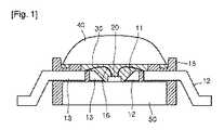
図1は本発明の第1実施例による発光素子パッケージを説明するための図である。It should be understood that such terms are intended to include other orientations of the element in addition to the orientation depicted in the drawings. Finally, the term “directly” means that there are no intervening elements. As used herein, the term “and / or” includes any and all combinations of any one or more of the recorded associated items.
(First embodiment)
FIG. 1 is a view illustrating a light emitting device package according to a first embodiment of the present invention.
図1に示すように、発光素子パッケージは、パッケージボディ15に具備された発光素子装着部11に発光素子20が装着され、前記発光素子20はパッケージボディ15を貫通して外部に連結される第1、2リードフレーム12、13にワイヤ16を介して電気的に連結される。前記発光素子20の下側には熱放出部50が配置されてもよい。 As shown in FIG. 1, in the light emitting device package, the
前記発光素子装着部11は前記第1、2リードフレーム12、13、前記熱放出部50及びパッケージボディ15によって形成される空間であり、前記発光素子20を装着できるキャビティを提供する。 The light emitting
前記第1、2リードフレーム12、13及び熱放出部50は銅材で形成してもよく、表面には銀又はアルミニウムで形成された反射率の高い反射膜を形成してもよい。 The first and
前記発光素子20を含む発光素子装着部11の上側は充填材30で充填され、このような充填材30上にはレンズ40が付着される。前記充填材30には蛍光体を含めてもよい。 The upper side of the light emitting
この時、パッケージボディ15は前記第1、2リードフレーム12、13及び前記熱放出部50が配置された状態で射出して形成する。 At this time, the
したがって、前記パッケージボディ15によって前記第1、2リードフレーム12、13及び前記熱放出部50を固定することができ、前記第1、2リードフレーム12、13は前記パッケージボディ15を貫通して外部に連結され得る。 Accordingly, the first and
前記パッケージボディ15は射出成形可能なプラスチック物質で形成することができる。 The
前記発光素子20は電極層の形成位置によって水平型発光素子、フリップチップボンディングされた発光素子、及び垂直型発光素子をすべて適用することができる。 The
ここで、垂直型発光素子は金属又は半導体からなる支持層上に発光素子が形成された構造であってもよい。 Here, the vertical light emitting device may have a structure in which the light emitting device is formed on a support layer made of metal or semiconductor.
実施例による発光素子パッケージは、レンズ40が付着されて形成される。このようなレンズ40は発光素子の光出力を向上させ、配光特性を調節できる長所がある。
(第2実施例)
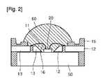
図2は本発明の第2実施例による発光素子パッケージを説明するための図である。The light emitting device package according to the embodiment is formed by attaching the
(Second embodiment)
FIG. 2 is a view illustrating a light emitting device package according to a second embodiment of the present invention.
以下、図2に基づき本発明の第2実施例を説明する。説明されない部分は第1実施例と同じでもよい。 Hereinafter, a second embodiment of the present invention will be described with reference to FIG. Portions that are not described may be the same as those in the first embodiment.
本発明の発光素子パッケージは第1実施例のように別途製作されたレンズを付着してもよく、または、図2のように、発光素子20上にシリコンジェル又はエポキシ樹脂をディスペンスして充填材を兼ねたレンズ60を形成してもよい。前記レンズ60には蛍光体を含めてもよい。 The light emitting device package of the present invention may be attached with a separately manufactured lens as in the first embodiment, or, as shown in FIG. Alternatively, the
特にディスペンス法を用いてレンズ60を形成することによって、レンズの製作を別途に行う必要がなく、発光素子20上に充填材を充填する工程を行う際にレンズ60の形成をも行うことができるので追加的な工程を行わずともレンズ60を形成して光出力を向上させることができる長所がある。 In particular, by forming the
ディスペンス法とは、ノズルを用いて液状のジェル又は樹脂を塗布して形成する方法であり、インクジェット法と類似の方法である。このようなディスペンス法は塗布されたジェル又は樹脂を硬化させる方法を含む。 The dispensing method is a method in which a liquid gel or resin is applied and formed using a nozzle, and is a method similar to the ink jet method. Such dispensing methods include methods of curing the applied gel or resin.
白色、緑色、赤色、黄色などの光を発光する発光素子パッケージを実現するために、青色又は近紫外線発光素子に蛍光体を塗布する方法がある。本発明の発光素子パッケージは蛍光体を発光素子20上に直に蛍光体をパウダーのような形態でシリコンジェル又はエポキシ樹脂と混合してコーティングすることができる。 In order to realize a light emitting device package that emits light such as white, green, red, and yellow, there is a method of applying a phosphor to a blue or near ultraviolet light emitting device. In the light emitting device package of the present invention, the phosphor can be coated directly on the
例えば、青色発光素子に黄色蛍光体が塗布される場合、青色発光素子から放出される青色光が黄色蛍光体を励起させて黄色光を発光させ、このような青色光と黄色光が混合されて白色光を作ることができる。 For example, when a yellow phosphor is applied to a blue light emitting element, blue light emitted from the blue light emitting element excites the yellow phosphor to emit yellow light, and such blue light and yellow light are mixed. Can produce white light.
また、蛍光体の発光が発光素子20チップに吸収されて効率が減少する現象を防ぐために発光素子20チップ上にシリコンジェル又はエポキシ樹脂を充填し、その上に蛍光体とシリコンジェル又はエポキシ樹脂を混合してコーティングすることでレンズを形成することによって高効率の白色発光素子パッケージを実現することができる。 Further, in order to prevent the phenomenon that the light emission of the phosphor is absorbed by the
この時、発光素子20上にシリコンジェル又はエポキシ樹脂をコーティングする際、発光素子20から放出された光を效果的に分散させ、樹脂の屈折率を高めて発光素子チップの光抽出を向上させるために分散剤又は拡散剤を混合してコーティングすることができる。
(第3実施例)
図3乃至図5は本発明の第3実施例による発光素子パッケージを説明するための図である。At this time, when a silicon gel or an epoxy resin is coated on the
(Third embodiment)
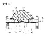
3 to 5 are views illustrating a light emitting device package according to a third embodiment of the present invention.
図3乃至図5に基づき本発明の第3実施例を説明する。説明されない部分は前の実施例と同じでもよい。 A third embodiment of the present invention will be described with reference to FIGS. Parts not described may be the same as in the previous embodiment.
図3に示すように、パッケージボディ15に具備された発光素子装着部11に発光素子20が装着され、このような発光素子20はパッケージボディ15を介して外部に連結される第1、2リードフレーム12、13にワイヤ16を介して電気的に連結される。 As shown in FIG. 3, the
このような発光素子20の上側には蛍光体を含む充填材31が充填される。このような充填材31はシリコンジェル又はエポキシ樹脂のような合成樹脂に蛍光体を混合して発光素子装着部11内に充填するものである。 A filling
この時、蛍光体は様々な色を発光できる蛍光体を用いることができる。すなわち、青色、緑色、黄色、赤色などを発光する物質を用いることができる。 At this time, phosphors that can emit various colors can be used. That is, a substance that emits blue, green, yellow, red, or the like can be used.
このような充填材31上にはシリコンジェル又はエポキシ樹脂を様々な方法でコーティングしてモールディング部41を形成することができる。すなわち、図3のように、モールディング部41をレンズ形状に形成してもよく、図4のように、板状のモールディング部42を形成してもよい。 The
一方、図5にはモールディング部43を図4に示す場合よりも低く形成してパッケージ全体の高さを低くすることができる例を示している。この時、このような高さの低いモールディング部43は、パッケージボディ15の高さを低く形成し、このパッケージボディ15の高さまでモールディング部43を形成することによって形成され得る。
(第4実施例)
図6乃至図8は本発明の第4実施例による発光素子パッケージを説明するための図である。On the other hand, FIG. 5 shows an example in which the
(Fourth embodiment)
6 to 8 are views illustrating a light emitting device package according to a fourth embodiment of the present invention.
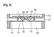
以下、図6乃至図8に基づき本発明の第4実施例を説明する。説明されない部分は前の実施例と同じでもよい。 Hereinafter, a fourth embodiment of the present invention will be described with reference to FIGS. Parts not described may be the same as in the previous embodiment.
図6に示すように、パッケージボディ15に具備された発光素子装着部11に発光素子20が装着され、このような発光素子20はパッケージボディ15を介して外部に連結される第1、2リードフレーム12、13にワイヤ16を介して電気的に連結される。 As shown in FIG. 6, the
このような発光素子20の上側の発光素子装着部11はシリコンジェル又はエポキシ樹脂からなる充填材32で充填される。このような充填材32には蛍光体が含まれない。 The light emitting
そして、このような充填材32上には蛍光体が含まれた蛍光体層33が形成されることができる。蛍光体層33は蛍光体がシリコンジェル又はエポキシ樹脂と混合されて形成され得る。 A
すなわち、蛍光体の発光が発光素子20に吸収されて発光効率が減少する現象を防止するために、発光素子20上にシリコンジェル又はエポキシ樹脂からなる充填材32を充填し、その上に蛍光体とシリコンジェル又はエポキシ樹脂が混合された蛍光体層33をコーティングすることで高効率の発光素子パッケージを実現できる。 That is, in order to prevent a phenomenon in which the light emission of the phosphor is absorbed by the
また、前記蛍光体が含まれた蛍光体層33が前記発光素子20と前記充填材32によって離隔して形成されるので、前記発光素子20から放出される熱によって前記蛍光体の特性が変化することを防止できる。 Further, since the
また、前記蛍光体が含まれた蛍光体層33が前記発光素子20と前記充填材32によって離隔して形成されるので、色均一度が向上し得る。 Further, since the
このような蛍光体層33上にはシリコンジェル又はエポキシ樹脂を用いて図6のように、レンズ形状のモールディング部42を形成することができる。または、図7に示すように、蛍光体層33上にモールディング部を形成しなくてもよい。 A lens-shaped
一方、図8に示すように、発光素子20上に充填材34を形成する場合に分散剤又は拡散剤70を混合することで、発光素子20から発光される光を效率的に分散させ、樹脂の屈折率を高めて発光素子20の光抽出を向上させることができる。 On the other hand, as shown in FIG. 8, when the
このような分散剤又は拡散剤70はSiO2、TiO2、及びZrO2のうち少なくともいずれか一つを用いることができ、充填材のみならず蛍光体層33又はモールディング部42を形成する際に含めてもよい。As such a dispersing agent or diffusing
このような充填材34上には蛍光体が含まれた蛍光体層33が形成されて発光素子20から放出される光の波長を変化させることができる。
(第5実施例)
図9乃至図11は本発明の第5実施例による発光素子パッケージを説明するための図である。A
(5th Example)
9 to 11 are views illustrating a light emitting device package according to a fifth embodiment of the present invention.
以下、図9乃至図11に基づき本発明の第5実施例を説明する。説明されない部分は前の実施例と同じでもよい。 Hereinafter, a fifth embodiment of the present invention will be described with reference to FIGS. Parts not described may be the same as in the previous embodiment.
図9に示すように、パッケージボディ15に具備された発光素子装着部11に発光素子20が装着され、このような発光素子20はパッケージボディ15を介して外部に連結される第1、2リードフレーム12、13にワイヤ16を介して電気的に連結される。 As shown in FIG. 9, the
このような発光素子20の上側の発光素子装着部11はシリコンジェル又はエポキシ樹脂からなるドーム(dome)形状の充填材35で充填される。 The light emitting
このようなドーム形状の充填材35は光抽出効率を向上させるためのものであり、この時、このようなドーム形状は半球(hemisphere)形状の方がより効果的な場合もある。半球面では光の放出が光の出発角度に関係なく常に垂直の角度をなすようになる。 The dome-shaped
したがって、垂直入射角度にあたる高い透過率を得ることができ、全反射角度はこれ以上存在しなくなる。 Therefore, a high transmittance corresponding to the normal incidence angle can be obtained, and the total reflection angle no longer exists.
図9では発光素子装着部11にシリコンジェル又はエポキシ樹脂を用いてドーム形状の充填材35を形成した後、蛍光体層の効率を上げるために充填材35上に蛍光体を含む蛍光体層33を形成する。 In FIG. 9, after forming a dome-shaped
このような蛍光体層33上にはレンズ形状のモールディング部41を形成することができる。 A lens-shaped
一方、図10に示すように、屈折率の高い分散剤又は拡散剤70が混合されたシリコンジェル又はエポキシ樹脂からなるドーム形状の充填材36を形成してもよい。 On the other hand, as shown in FIG. 10, a dome-shaped
または、図11に示す同じように、発光素子20が装着された発光素子装着部11にドーム形状の蛍光体層37を形成してもよい。蛍光体層37の屈折率はシリコンジェルよりも高いので光抽出効率を向上させるために効果的な場合がある。このようなドーム形状の蛍光体層37上にはレンズ形状のモールディング部41が位置し得る。
(第6実施例)
図12乃至図14は本発明の第6実施例による発光素子パッケージを説明するための図である。Alternatively, as shown in FIG. 11, the dome-shaped
(Sixth embodiment)
12 to 14 are views illustrating a light emitting device package according to a sixth embodiment of the present invention.
以下、図12乃至図14に基づき本発明の第6実施例を説明する。説明されない部分は前の実施例と同じでもよい。 Hereinafter, a sixth embodiment of the present invention will be described with reference to FIGS. Parts not described may be the same as in the previous embodiment.
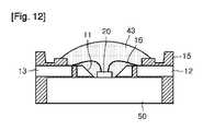
図12に示すように、パッケージボディ15に具備された発光素子装着部11に発光素子20が装着され、このような発光素子20はパッケージボディ15を介して外部に連結される第1、2リードフレーム12、13にワイヤ16を介して電気的に連結される。 As shown in FIG. 12, the
このような発光素子20の上側の発光素子装着部11はシリコンジェル又はエポキシ樹脂からなるドーム形状のモールディング部43で充填される。このモールディング部43には蛍光体が混合されており、ディスペンス法を用いてドーム形状にモールディングして様々な色を実現することができ、レンズの役割を兼ねることができる。 The light emitting
図12では発光素子装着部11の上側のすべての空間をモールディング部43で充填してレンズ形状まで形成した状態を示している。 FIG. 12 shows a state in which the entire space above the light emitting
一方、図13では発光素子20が装着された発光素子装着部11にシリコンジェルのような物質からなる充填材38を充填し、その上側に蛍光体を含むモールディング部43を形成した例を示している。 On the other hand, FIG. 13 shows an example in which the light emitting
この時、モールディング部43には分散剤又は拡散剤を含めてもよい。 At this time, the
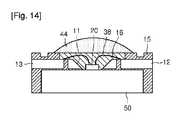
図14では発光素子装着部11に充填材38を形成するが、パッケージボディ15のより高い部分まで充填材38を充填し、その上側に蛍光体を含むレンズ形状のモールディング部44を形成した状態を示している。 In FIG. 14, the filling
このように、図14に示す例でのモールディング部44はレンズ形状に製作されてもよい。 Thus, the
上述したように、本発明は発光素子パッケージを製作する際、充填材及びレンズ形状を形成するにおいて、別途製作したレンズを付着することもでき、シリコンジェル又はエポキシ樹脂を塗布する過程でディスペンス法でレンズ形状を製造することができるので追加的な工程を行うことなく発光効率を増大させることができる構造を提供する。 As described above, according to the present invention, when the light emitting device package is manufactured, a separately manufactured lens can be attached in forming the filler and the lens shape, and the dispensing method is used in the process of applying the silicon gel or the epoxy resin. Since a lens shape can be manufactured, a structure capable of increasing luminous efficiency without performing an additional process is provided.
したがって、本発明の発光素子パッケージは、特に、高出力、高効率を必要とする装飾照明、一般照明、自動車電装、LCD用バックライトなどに適用できる。 Therefore, the light emitting device package of the present invention is particularly applicable to decorative lighting, general lighting, automobile electrical equipment, LCD backlights, and the like that require high output and high efficiency.
上述した実施例は本発明の技術的思想を具体的に説明するための一例であり、本発明は上述した実施例に限定されるものではなく、様々な形態への変形が可能であり、当然のことながら、このような技術的思想の様々な実施の形態は、すべて本発明の保護範囲内に含まれるものである。 The above-described embodiments are examples for specifically explaining the technical idea of the present invention. The present invention is not limited to the above-described embodiments, and can be modified in various forms. Nevertheless, various embodiments of such a technical idea are all included in the protection scope of the present invention.
本発明の実施例による発光素子パッケージは、照明装置のみならず様々な電子機器の光源として用いることができる。 The light emitting device package according to the embodiment of the present invention can be used not only as a lighting device but also as a light source of various electronic devices.
Claims (20)
Translated fromJapanese前記パッケージボディに形成されたリードフレームと、
前記パッケージボディに支持され前記リードフレームと電気的に連結される発光素子と、
前記発光素子を囲んで形成される充填材と、
前記充填材上に蛍光体を含んで形成された蛍光体層と、を含む発光素子パッケージ。A package body;
A lead frame formed on the package body;
A light emitting device supported by the package body and electrically connected to the lead frame;
A filler formed around the light emitting element;
And a phosphor layer formed on the filler so as to contain the phosphor.
前記パッケージボディに形成されたリードフレームと、
前記パッケージボディに支持され前記リードフレームと電気的に連結される発光素子と、
前記発光素子を囲み上面がドーム形状に形成された充填材と、
前記充填材上に蛍光体を含んで形成された蛍光体層と、
前記蛍光体層上に上面がドーム形状に形成されたモールディング部と、を含む発光素子パッケージ。A package body;
A lead frame formed on the package body;
A light emitting device supported by the package body and electrically connected to the lead frame;
A filler surrounding the light emitting element and having an upper surface formed in a dome shape;
A phosphor layer formed on the filler containing a phosphor;
A light emitting device package comprising: a molding part having an upper surface formed in a dome shape on the phosphor layer.
Applications Claiming Priority (2)
| Application Number | Priority Date | Filing Date | Title |
|---|---|---|---|
| KR1020070067986AKR100880638B1 (en) | 2007-07-06 | 2007-07-06 | Light emitting device package |
| PCT/KR2008/003960WO2009008636A2 (en) | 2007-07-06 | 2008-07-04 | Light emitting device package |
Related Child Applications (1)
| Application Number | Title | Priority Date | Filing Date |
|---|---|---|---|
| JP2013105966ADivisionJP2013191872A (en) | 2007-07-06 | 2013-05-20 | Light emitting element package |
Publications (1)
| Publication Number | Publication Date |
|---|---|
| JP2010532929Atrue JP2010532929A (en) | 2010-10-14 |
Family
ID=40229253
Family Applications (2)
| Application Number | Title | Priority Date | Filing Date |
|---|---|---|---|
| JP2010515966APendingJP2010532929A (en) | 2007-07-06 | 2008-07-04 | Light emitting device package |
| JP2013105966APendingJP2013191872A (en) | 2007-07-06 | 2013-05-20 | Light emitting element package |
Family Applications After (1)
| Application Number | Title | Priority Date | Filing Date |
|---|---|---|---|
| JP2013105966APendingJP2013191872A (en) | 2007-07-06 | 2013-05-20 | Light emitting element package |
Country Status (7)
| Country | Link |
|---|---|
| US (3) | US8610255B2 (en) |
| EP (3) | EP2624317A3 (en) |
| JP (2) | JP2010532929A (en) |
| KR (1) | KR100880638B1 (en) |
| CN (2) | CN104393146A (en) |
| DE (2) | DE202008018207U1 (en) |
| WO (1) | WO2009008636A2 (en) |
Cited By (8)
| Publication number | Priority date | Publication date | Assignee | Title |
|---|---|---|---|---|
| CN102447049A (en)* | 2011-12-31 | 2012-05-09 | 杭州电子科技大学 | LED packaging structure and LED lighting device based on COB packaging technology |
| JP2013191872A (en)* | 2007-07-06 | 2013-09-26 | Lg Innotek Co Ltd | Light emitting element package |
| JP2014220490A (en)* | 2013-04-12 | 2014-11-20 | 日亜化学工業株式会社 | Light emitting device |
| JP2015012144A (en)* | 2013-06-28 | 2015-01-19 | 日亜化学工業株式会社 | Light-emitting device and method of manufacturing the same |
| JP2015022989A (en)* | 2013-07-23 | 2015-02-02 | パナソニック株式会社 | Lighting fixture |
| JP2017112211A (en)* | 2015-12-16 | 2017-06-22 | 豊田合成株式会社 | Method of manufacturing light-emitting device |
| JP2019212752A (en)* | 2018-06-05 | 2019-12-12 | 日亜化学工業株式会社 | Light-emitting device |
| JP2021508182A (en)* | 2018-02-19 | 2021-02-25 | シグニファイ ホールディング ビー ヴィSignify Holding B.V. | Encapsulation device with light engine |
Families Citing this family (34)
| Publication number | Priority date | Publication date | Assignee | Title |
|---|---|---|---|---|
| KR100888236B1 (en)* | 2008-11-18 | 2009-03-12 | 서울반도체 주식회사 | Light emitting device |
| TWI403005B (en)* | 2009-10-12 | 2013-07-21 | Intematix Technology Ct Corp | Light-emitting diode and manufacturing method thereof |
| KR100986468B1 (en)* | 2009-11-19 | 2010-10-08 | 엘지이노텍 주식회사 | Lense and light emitting apparatus including the lense |
| KR100986380B1 (en) | 2009-11-20 | 2010-10-08 | 엘지이노텍 주식회사 | Light emitting apparatus |
| KR101258586B1 (en)* | 2009-12-21 | 2013-05-02 | 엘지디스플레이 주식회사 | Light emitting diode package and method of fabricating the same |
| CN101867008B (en)* | 2010-05-17 | 2012-11-21 | 中山大学佛山研究院 | LED packaging module capable of releasing stress |
| KR101147614B1 (en)* | 2010-06-16 | 2012-05-23 | 솔레즈 주식회사 | Light Emitting Diode Chip Package |
| TWI505509B (en)* | 2010-06-21 | 2015-10-21 | Hon Hai Prec Ind Co Ltd | Light-emitting diode and light source module |
| FI20106001A0 (en)* | 2010-09-28 | 2010-09-28 | Kruunutekniikka Oy | Method for manufacturing an electronic actuator |
| KR101107851B1 (en) | 2010-11-12 | 2012-02-07 | 삼성엘이디 주식회사 | Phosphor Automatic Mixer and Phosphor Automatic Mixing Method |
| KR101618029B1 (en)* | 2010-12-06 | 2016-05-09 | 삼성전자주식회사 | Light Emitting Device Package and Manufacturing Method thereof |
| KR101626412B1 (en)* | 2010-12-24 | 2016-06-02 | 삼성전자주식회사 | Light emitting device package and method of manufacturing the same |
| CN102610602A (en)* | 2011-01-25 | 2012-07-25 | 四川柏狮光电技术有限公司 | High-resolution LED (light emitting diode) light source made of single-package-based material and manufacturing process of high-resolution LED light source |
| JP5666962B2 (en)* | 2011-03-28 | 2015-02-12 | 日東電工株式会社 | Light emitting diode device and manufacturing method thereof |
| KR101896661B1 (en)* | 2011-10-28 | 2018-09-07 | 엘지이노텍 주식회사 | Light emitting device package, back light unit and display unit |
| KR20130107536A (en)* | 2012-03-22 | 2013-10-02 | 삼성전자주식회사 | Led pakage and method of manufacturing same |
| CN103050606A (en)* | 2013-01-11 | 2013-04-17 | 华南师范大学 | High-color-rendering high-power LED (light emitting diode) encapsulation structure and manufacture method of high-color-rendering high-power LED encapsulation structure |
| KR20140140836A (en)* | 2013-05-30 | 2014-12-10 | 엘지이노텍 주식회사 | Light emitting device package |
| SG11201601050PA (en)* | 2013-09-10 | 2016-03-30 | Heptagon Micro Optics Pte Ltd | Compact opto-electronic modules and fabrication methods for such modules |
| DE102013225552A1 (en)* | 2013-12-11 | 2015-06-11 | Osram Opto Semiconductors Gmbh | Optoelectronic component |
| CN103633234A (en)* | 2013-12-18 | 2014-03-12 | 苏州东山精密制造股份有限公司 | LED (light emitting diode) package structure and method |
| KR102289345B1 (en)* | 2014-02-06 | 2021-08-13 | 루미리즈 홀딩 비.브이. | Light emitting diode with structured substrate |
| DE102014019242A1 (en) | 2014-12-19 | 2016-06-23 | Audi Ag | Display element for a motor vehicle, display device with such a display element, motor vehicle and method for generating a display element |
| DE102015112042B4 (en)* | 2015-07-23 | 2021-07-01 | OSRAM Opto Semiconductors Gesellschaft mit beschränkter Haftung | Optoelectronic lighting device |
| KR101778848B1 (en)* | 2015-08-21 | 2017-09-14 | 엘지전자 주식회사 | Light emitting device package assembly and method of fabricating the same |
| CN106324905A (en)* | 2016-08-31 | 2017-01-11 | 张家港康得新光电材料有限公司 | Quantum-dot light-emitting device and backlight module |
| US10707277B2 (en) | 2016-10-04 | 2020-07-07 | Vuereal Inc. | Method of integrating functional tuning materials with micro devices and structures thereof |
| JP2018064007A (en)* | 2016-10-12 | 2018-04-19 | ソニーセミコンダクタソリューションズ株式会社 | Solid-state image sensor, and electronic device |
| DE102017105035B4 (en)* | 2017-03-09 | 2024-09-26 | OSRAM Opto Semiconductors Gesellschaft mit beschränkter Haftung | LIGHT-EMITTING COMPONENT AND METHOD FOR PRODUCING A LIGHT-EMITTING COMPONENT |
| DE102018104382A1 (en)* | 2018-02-27 | 2019-08-29 | Osram Opto Semiconductors Gmbh | OPTOELECTRONIC COMPONENT AND MANUFACTURING METHOD |
| CN111341750B (en)* | 2018-12-19 | 2024-03-01 | 奥特斯奥地利科技与系统技术有限公司 | Component carrier comprising an electrically conductive base structure and method of manufacture |
| KR102746562B1 (en)* | 2019-03-22 | 2024-12-24 | 삼성전자주식회사 | Light emitting device package |
| KR20220012258A (en)* | 2019-05-23 | 2022-02-03 | 뷰리얼 인크. | Methods for integrating microdevices and their structures and functional coordination materials |
| CN112768592A (en)* | 2021-01-25 | 2021-05-07 | 赣州和晟精密电子有限公司 | LED support |
Citations (9)
| Publication number | Priority date | Publication date | Assignee | Title |
|---|---|---|---|---|
| JP2003324215A (en)* | 2002-04-30 | 2003-11-14 | Toyoda Gosei Co Ltd | Light emitting diode lamp |
| JP2005050827A (en)* | 2004-10-22 | 2005-02-24 | Matsushita Electric Works Ltd | Process for manufacturing illumination light source and illumination light source |
| JP2005183900A (en)* | 2003-10-30 | 2005-07-07 | Kyocera Corp | Light emitting device and lighting device |
| JP2005252219A (en)* | 2004-02-06 | 2005-09-15 | Toyoda Gosei Co Ltd | Light emitting device and sealing member |
| JP2005332963A (en)* | 2004-05-19 | 2005-12-02 | Shoei Chem Ind Co | Light emitting device |
| WO2006059828A1 (en)* | 2004-09-10 | 2006-06-08 | Seoul Semiconductor Co., Ltd. | Light emitting diode package having multiple molding resins |
| JP2006237199A (en)* | 2005-02-24 | 2006-09-07 | Asahi Rubber:Kk | Light-emitting diode lens and light-emitting diode light source device |
| JP2006324438A (en)* | 2005-05-18 | 2006-11-30 | Hitachi Cable Precision Co Ltd | Manufacturing method of surface mount type LED package with heat sink |
| JP2007142474A (en)* | 2003-04-24 | 2007-06-07 | Nichia Chem Ind Ltd | Semiconductor device and manufacturing method thereof |
Family Cites Families (48)
| Publication number | Priority date | Publication date | Assignee | Title |
|---|---|---|---|---|
| JPH07254732A (en)* | 1994-03-15 | 1995-10-03 | Toshiba Corp | Semiconductor light emitting device |
| DE19755734A1 (en) | 1997-12-15 | 1999-06-24 | Siemens Ag | Method for producing a surface-mountable optoelectronic component |
| DE19918370B4 (en)* | 1999-04-22 | 2006-06-08 | Osram Opto Semiconductors Gmbh | LED white light source with lens |
| US6517218B2 (en)* | 2000-03-31 | 2003-02-11 | Relume Corporation | LED integrated heat sink |
| US6614103B1 (en) | 2000-09-01 | 2003-09-02 | General Electric Company | Plastic packaging of LED arrays |
| EP1187226B1 (en)* | 2000-09-01 | 2012-12-26 | Citizen Electronics Co., Ltd. | Surface-mount type light emitting diode and method of manufacturing same |
| KR100419611B1 (en)* | 2001-05-24 | 2004-02-25 | 삼성전기주식회사 | A Light Emitting Diode, a Lighting Emitting Device Using the Same and a Fabrication Process therefor |
| US6791116B2 (en) | 2002-04-30 | 2004-09-14 | Toyoda Gosei Co., Ltd. | Light emitting diode |
| CN2563753Y (en)* | 2002-08-09 | 2003-07-30 | 佛山市光电器材公司 | Power type light-emitting diode |
| KR20040044701A (en) | 2002-11-21 | 2004-05-31 | 삼성전기주식회사 | A light emitting device package and a method of manufacturing the same |
| US7994526B2 (en) | 2003-05-28 | 2011-08-09 | Seoul Semiconductor Co., Ltd. | Light emitting diode package and light emitting diode system having at least two heat sinks |
| KR100524656B1 (en)* | 2003-09-30 | 2005-10-31 | 서울반도체 주식회사 | Polychromatic Light Emitting Diode Package and Polychromatic Light Emitting Diode System |
| JP2005159045A (en) | 2003-11-26 | 2005-06-16 | Sumitomo Electric Ind Ltd | Semiconductor light emitting element mounting member and light emitting diode using the same |
| KR100586944B1 (en) | 2003-12-26 | 2006-06-07 | 삼성전기주식회사 | High power light emitting diode package and manufacturing method |
| US7279346B2 (en)* | 2004-03-31 | 2007-10-09 | Cree, Inc. | Method for packaging a light emitting device by one dispense then cure step followed by another |
| KR100631521B1 (en) | 2004-04-17 | 2006-10-11 | 엘지전자 주식회사 | Light emitting device and manufacturing method thereof |
| JP2005317661A (en) | 2004-04-27 | 2005-11-10 | Sharp Corp | Semiconductor light emitting device and manufacturing method thereof |
| US20050264194A1 (en)* | 2004-05-25 | 2005-12-01 | Ng Kee Y | Mold compound with fluorescent material and a light-emitting device made therefrom |
| US7456499B2 (en)* | 2004-06-04 | 2008-11-25 | Cree, Inc. | Power light emitting die package with reflecting lens and the method of making the same |
| JP4359195B2 (en) | 2004-06-11 | 2009-11-04 | 株式会社東芝 | Semiconductor light emitting device, manufacturing method thereof, and semiconductor light emitting unit |
| JP4254669B2 (en) | 2004-09-07 | 2009-04-15 | 豊田合成株式会社 | Light emitting device |
| US7119422B2 (en)* | 2004-11-15 | 2006-10-10 | Unity Opto Technology Co., Ltd. | Solid-state semiconductor light emitting device |
| JP2008523637A (en) | 2004-12-14 | 2008-07-03 | ソウル オプト−デバイス カンパニー リミテッド | Light emitting device having a plurality of light emitting cells and package mounting the same |
| EP1825524A4 (en) | 2004-12-16 | 2010-06-16 | Seoul Semiconductor Co Ltd | CONNECTION GRID COMPRISING A THERMAL DISSIPATOR SUPPORT RING, METHOD FOR MANUFACTURING LIGHT-EMITTING DIODE HOUSING USING THE SAME, AND LIGHT-EMITTING DIODE HOUSING MADE THEREBY |
| KR100631903B1 (en)* | 2005-02-17 | 2006-10-11 | 삼성전기주식회사 | High power LED housing and its manufacturing method |
| KR101142519B1 (en) | 2005-03-31 | 2012-05-08 | 서울반도체 주식회사 | Backlight panel employing white light emitting diode having red phosphor and green phosphor |
| WO2007015732A2 (en) | 2005-08-01 | 2007-02-08 | Intex Recreation Corp. | A method of varying the color of light emitted by a light-emitting device |
| US7646035B2 (en) | 2006-05-31 | 2010-01-12 | Cree, Inc. | Packaged light emitting devices including multiple index lenses and multiple index lenses for packaged light emitting devices |
| KR100601891B1 (en) | 2005-08-04 | 2006-07-19 | 삼성전자주식회사 | LED package and manufacturing method thereof |
| JP2007067326A (en) | 2005-09-02 | 2007-03-15 | Shinko Electric Ind Co Ltd | Light emitting diode and manufacturing method thereof |
| JP2007116138A (en) | 2005-09-22 | 2007-05-10 | Lexedis Lighting Gmbh | Light emitting device |
| KR100665262B1 (en)* | 2005-10-20 | 2007-01-09 | 삼성전기주식회사 | LED Package |
| JP2007123438A (en)* | 2005-10-26 | 2007-05-17 | Toyoda Gosei Co Ltd | Phosphor plate and light emitting device having the same |
| JP3120556U (en) | 2005-11-29 | 2006-04-13 | 東貝光電科技股▲ふん▼有限公司 | Mixed light emitting diode structure |
| JP5228489B2 (en)* | 2005-12-12 | 2013-07-03 | 日亜化学工業株式会社 | Light emitting device, semiconductor device, and manufacturing method thereof |
| JP4847793B2 (en)* | 2006-06-01 | 2011-12-28 | 京セラ株式会社 | Light emitting device |
| US7960819B2 (en)* | 2006-07-13 | 2011-06-14 | Cree, Inc. | Leadframe-based packages for solid state emitting devices |
| US20080089072A1 (en) | 2006-10-11 | 2008-04-17 | Alti-Electronics Co., Ltd. | High Power Light Emitting Diode Package |
| US7889421B2 (en)* | 2006-11-17 | 2011-02-15 | Rensselaer Polytechnic Institute | High-power white LEDs and manufacturing method thereof |
| US7597468B2 (en)* | 2007-03-23 | 2009-10-06 | Promate Electronic Co., Ltd. | Light source of side-edge type LED backlight unit |
| US7868341B2 (en)* | 2007-06-27 | 2011-01-11 | The Regents Of The University Of California | Optical designs for high-efficacy white-light emitting diodes |
| KR100880638B1 (en) | 2007-07-06 | 2009-01-30 | 엘지전자 주식회사 | Light emitting device package |
| JP5251038B2 (en) | 2007-08-23 | 2013-07-31 | 豊田合成株式会社 | Light emitting device |
| KR101028329B1 (en)* | 2010-04-28 | 2011-04-12 | 엘지이노텍 주식회사 | Light emitting device package and its manufacturing method |
| CN102893701B (en)* | 2010-05-04 | 2016-05-04 | 吉可多公司 | LED lighting device with communication port for sending associated information |
| KR101114197B1 (en)* | 2010-08-09 | 2012-02-22 | 엘지이노텍 주식회사 | Light emitting device and lighting system having same |
| US8198109B2 (en)* | 2010-08-27 | 2012-06-12 | Quarkstar Llc | Manufacturing methods for solid state light sheet or strip with LEDs connected in series for general illumination |
| US9240530B2 (en)* | 2012-02-13 | 2016-01-19 | Cree, Inc. | Light emitter devices having improved chemical and physical resistance and related methods |
- 2007
- 2007-07-06KRKR1020070067986Apatent/KR100880638B1/enactiveActive
- 2008
- 2008-07-04EPEP13166476.5Apatent/EP2624317A3/ennot_activeCeased
- 2008-07-04EPEP08778623Apatent/EP2171773A4/ennot_activeCeased
- 2008-07-04DEDE202008018207Upatent/DE202008018207U1/ennot_activeExpired - Lifetime
- 2008-07-04CNCN201410571869.1Apatent/CN104393146A/enactivePending
- 2008-07-04CNCN200880025437Apatent/CN101755346A/enactivePending
- 2008-07-04JPJP2010515966Apatent/JP2010532929A/enactivePending
- 2008-07-04EPEP11183012Apatent/EP2403020A3/ennot_activeCeased
- 2008-07-04WOPCT/KR2008/003960patent/WO2009008636A2/enactiveApplication Filing
- 2008-07-04DEDE202008018130Upatent/DE202008018130U1/ennot_activeExpired - Lifetime
- 2008-07-04USUS12/667,743patent/US8610255B2/enactiveActive
- 2011
- 2011-12-20USUS13/331,984patent/US8890297B2/enactiveActive
- 2013
- 2013-05-20JPJP2013105966Apatent/JP2013191872A/enactivePending
- 2013-11-22USUS14/087,532patent/US9368697B2/ennot_activeExpired - Fee Related
Patent Citations (9)
| Publication number | Priority date | Publication date | Assignee | Title |
|---|---|---|---|---|
| JP2003324215A (en)* | 2002-04-30 | 2003-11-14 | Toyoda Gosei Co Ltd | Light emitting diode lamp |
| JP2007142474A (en)* | 2003-04-24 | 2007-06-07 | Nichia Chem Ind Ltd | Semiconductor device and manufacturing method thereof |
| JP2005183900A (en)* | 2003-10-30 | 2005-07-07 | Kyocera Corp | Light emitting device and lighting device |
| JP2005252219A (en)* | 2004-02-06 | 2005-09-15 | Toyoda Gosei Co Ltd | Light emitting device and sealing member |
| JP2005332963A (en)* | 2004-05-19 | 2005-12-02 | Shoei Chem Ind Co | Light emitting device |
| WO2006059828A1 (en)* | 2004-09-10 | 2006-06-08 | Seoul Semiconductor Co., Ltd. | Light emitting diode package having multiple molding resins |
| JP2005050827A (en)* | 2004-10-22 | 2005-02-24 | Matsushita Electric Works Ltd | Process for manufacturing illumination light source and illumination light source |
| JP2006237199A (en)* | 2005-02-24 | 2006-09-07 | Asahi Rubber:Kk | Light-emitting diode lens and light-emitting diode light source device |
| JP2006324438A (en)* | 2005-05-18 | 2006-11-30 | Hitachi Cable Precision Co Ltd | Manufacturing method of surface mount type LED package with heat sink |
Cited By (18)
| Publication number | Priority date | Publication date | Assignee | Title |
|---|---|---|---|---|
| JP2013191872A (en)* | 2007-07-06 | 2013-09-26 | Lg Innotek Co Ltd | Light emitting element package |
| US8890297B2 (en) | 2007-07-06 | 2014-11-18 | Lg Innotek Co., Ltd. | Light emitting device package |
| US9368697B2 (en) | 2007-07-06 | 2016-06-14 | Lg Innotek Co., Ltd. | Light emitting device package |
| CN102447049B (en)* | 2011-12-31 | 2013-08-14 | 杭州电子科技大学 | LED (light-emitting diode) package structure based on COB (chip on board) package technology and LED illuminator |
| CN102447049A (en)* | 2011-12-31 | 2012-05-09 | 杭州电子科技大学 | LED packaging structure and LED lighting device based on COB packaging technology |
| JP2020010053A (en)* | 2013-04-12 | 2020-01-16 | 日亜化学工業株式会社 | Light emitting device |
| JP2014220490A (en)* | 2013-04-12 | 2014-11-20 | 日亜化学工業株式会社 | Light emitting device |
| JP2015012144A (en)* | 2013-06-28 | 2015-01-19 | 日亜化学工業株式会社 | Light-emitting device and method of manufacturing the same |
| JP2015022989A (en)* | 2013-07-23 | 2015-02-02 | パナソニック株式会社 | Lighting fixture |
| JP2017112211A (en)* | 2015-12-16 | 2017-06-22 | 豊田合成株式会社 | Method of manufacturing light-emitting device |
| JP2021508182A (en)* | 2018-02-19 | 2021-02-25 | シグニファイ ホールディング ビー ヴィSignify Holding B.V. | Encapsulation device with light engine |
| JP7218378B2 (en) | 2018-02-19 | 2023-02-06 | シグニファイ ホールディング ビー ヴィ | Sealed device with light engine |
| JP2019212752A (en)* | 2018-06-05 | 2019-12-12 | 日亜化学工業株式会社 | Light-emitting device |
| JP7231809B2 (en) | 2018-06-05 | 2023-03-02 | 日亜化学工業株式会社 | light emitting device |
| JP2023052858A (en)* | 2018-06-05 | 2023-04-12 | 日亜化学工業株式会社 | light emitting device |
| JP2023052842A (en)* | 2018-06-05 | 2023-04-12 | 日亜化学工業株式会社 | light emitting device |
| JP7364971B2 (en) | 2018-06-05 | 2023-10-19 | 日亜化学工業株式会社 | light emitting device |
| JP7364970B2 (en) | 2018-06-05 | 2023-10-19 | 日亜化学工業株式会社 | light emitting device |
Also Published As
| Publication number | Publication date |
|---|---|
| JP2013191872A (en) | 2013-09-26 |
| US20140077245A1 (en) | 2014-03-20 |
| US20120086039A1 (en) | 2012-04-12 |
| EP2403020A2 (en) | 2012-01-04 |
| CN101755346A (en) | 2010-06-23 |
| EP2403020A3 (en) | 2013-02-20 |
| EP2171773A4 (en) | 2011-03-09 |
| KR100880638B1 (en) | 2009-01-30 |
| DE202008018207U1 (en) | 2012-01-24 |
| US8610255B2 (en) | 2013-12-17 |
| KR20090004078A (en) | 2009-01-12 |
| EP2171773A2 (en) | 2010-04-07 |
| WO2009008636A3 (en) | 2009-03-05 |
| WO2009008636A2 (en) | 2009-01-15 |
| CN104393146A (en) | 2015-03-04 |
| EP2624317A2 (en) | 2013-08-07 |
| US9368697B2 (en) | 2016-06-14 |
| US20110140142A1 (en) | 2011-06-16 |
| US8890297B2 (en) | 2014-11-18 |
| EP2624317A3 (en) | 2013-08-28 |
| DE202008018130U1 (en) | 2011-12-20 |
Similar Documents
| Publication | Publication Date | Title |
|---|---|---|
| JP2010532929A (en) | Light emitting device package | |
| US9287475B2 (en) | Solid state lighting component package with reflective polymer matrix layer | |
| US8803201B2 (en) | Solid state lighting component package with reflective layer | |
| KR101251821B1 (en) | Light emitting device package | |
| KR100723247B1 (en) | Chip coated LED package and manufacturing method thereof | |
| KR20150056055A (en) | Light-emitting device | |
| KR20100004889A (en) | Wavelength converted light emitting diode chip and light emitting device having the same | |
| JP2006135288A (en) | White light emitting diode package and manufacturing method thereof | |
| JP2007088472A (en) | Light emitting diode package and manufacturing method thereof | |
| JP2014041993A (en) | Light-emitting device and method of manufacturing the same | |
| JP2013232484A (en) | Light-emitting device and method for manufacturing the same | |
| JP6212989B2 (en) | Light emitting device and manufacturing method thereof | |
| US20070194691A1 (en) | Light emitting diode package structure having high light extraction efficiency and method of manufacturing the same | |
| CN102651447B (en) | Light emitting diode | |
| JP2019036676A (en) | Light emitting device | |
| CN104934516A (en) | LED package having transparent heat insulation adhesive layer | |
| KR20120061626A (en) | Light emitting device and light emitting diode package | |
| KR20130077058A (en) | Led package and method for manufacturing the same | |
| JP6739527B2 (en) | Light emitting device | |
| US11996502B2 (en) | Method of manufacturing light-emitting device including step of curing sealing member while applying centrifugal force | |
| KR101554904B1 (en) | Method for manufacturing a light emitting diode package having an excellent heat dissipation capability | |
| KR20110087973A (en) | LED package, manufacturing method thereof and lighting device having LED package | |
| KR20080102757A (en) | Light emitting diode device and manufacturing method thereof |
Legal Events
| Date | Code | Title | Description |
|---|---|---|---|
| A977 | Report on retrieval | Free format text:JAPANESE INTERMEDIATE CODE: A971007 Effective date:20120326 | |
| A131 | Notification of reasons for refusal | Free format text:JAPANESE INTERMEDIATE CODE: A131 Effective date:20120410 | |
| A521 | Request for written amendment filed | Free format text:JAPANESE INTERMEDIATE CODE: A523 Effective date:20120709 | |
| A02 | Decision of refusal | Free format text:JAPANESE INTERMEDIATE CODE: A02 Effective date:20130122 |