JP2010530634A - Oxide semiconductor and thin film transistor including the same - Google Patents
Oxide semiconductor and thin film transistor including the sameDownload PDFInfo
- Publication number
- JP2010530634A JP2010530634AJP2010513115AJP2010513115AJP2010530634AJP 2010530634 AJP2010530634 AJP 2010530634AJP 2010513115 AJP2010513115 AJP 2010513115AJP 2010513115 AJP2010513115 AJP 2010513115AJP 2010530634 AJP2010530634 AJP 2010530634A
- Authority
- JP
- Japan
- Prior art keywords
- oxide
- oxide semiconductor
- thin film
- film transistor
- channel
- Prior art date
- Legal status (The legal status is an assumption and is not a legal conclusion. Google has not performed a legal analysis and makes no representation as to the accuracy of the status listed.)
- Pending
Links
Images


Classifications
- H—ELECTRICITY
- H10—SEMICONDUCTOR DEVICES; ELECTRIC SOLID-STATE DEVICES NOT OTHERWISE PROVIDED FOR
- H10D—INORGANIC ELECTRIC SEMICONDUCTOR DEVICES
- H10D30/00—Field-effect transistors [FET]
- H10D30/60—Insulated-gate field-effect transistors [IGFET]
- H10D30/67—Thin-film transistors [TFT]
- H10D30/674—Thin-film transistors [TFT] characterised by the active materials
- H10D30/6755—Oxide semiconductors, e.g. zinc oxide, copper aluminium oxide or cadmium stannate
- H—ELECTRICITY
- H01—ELECTRIC ELEMENTS
- H01L—SEMICONDUCTOR DEVICES NOT COVERED BY CLASS H10
- H01L21/00—Processes or apparatus adapted for the manufacture or treatment of semiconductor or solid state devices or of parts thereof
- H01L21/02—Manufacture or treatment of semiconductor devices or of parts thereof
- H01L21/02104—Forming layers
- H01L21/02365—Forming inorganic semiconducting materials on a substrate
- H01L21/02367—Substrates
- H01L21/0237—Materials
- H—ELECTRICITY
- H01—ELECTRIC ELEMENTS
- H01L—SEMICONDUCTOR DEVICES NOT COVERED BY CLASS H10
- H01L21/00—Processes or apparatus adapted for the manufacture or treatment of semiconductor or solid state devices or of parts thereof
- H01L21/02—Manufacture or treatment of semiconductor devices or of parts thereof
- H01L21/02104—Forming layers
- H01L21/02365—Forming inorganic semiconducting materials on a substrate
- H01L21/02436—Intermediate layers between substrates and deposited layers
- H01L21/02439—Materials
- H01L21/02488—Insulating materials
- H—ELECTRICITY
- H01—ELECTRIC ELEMENTS
- H01L—SEMICONDUCTOR DEVICES NOT COVERED BY CLASS H10
- H01L21/00—Processes or apparatus adapted for the manufacture or treatment of semiconductor or solid state devices or of parts thereof
- H01L21/02—Manufacture or treatment of semiconductor devices or of parts thereof
- H01L21/02104—Forming layers
- H01L21/02365—Forming inorganic semiconducting materials on a substrate
- H01L21/02518—Deposited layers
- H01L21/02521—Materials
- H01L21/02551—Group 12/16 materials
- H01L21/02554—Oxides
- H—ELECTRICITY
- H01—ELECTRIC ELEMENTS
- H01L—SEMICONDUCTOR DEVICES NOT COVERED BY CLASS H10
- H01L21/00—Processes or apparatus adapted for the manufacture or treatment of semiconductor or solid state devices or of parts thereof
- H01L21/02—Manufacture or treatment of semiconductor devices or of parts thereof
- H01L21/02104—Forming layers
- H01L21/02365—Forming inorganic semiconducting materials on a substrate
- H01L21/02518—Deposited layers
- H01L21/02521—Materials
- H01L21/02565—Oxide semiconducting materials not being Group 12/16 materials, e.g. ternary compounds
- H—ELECTRICITY
- H01—ELECTRIC ELEMENTS
- H01L—SEMICONDUCTOR DEVICES NOT COVERED BY CLASS H10
- H01L21/00—Processes or apparatus adapted for the manufacture or treatment of semiconductor or solid state devices or of parts thereof
- H01L21/02—Manufacture or treatment of semiconductor devices or of parts thereof
- H01L21/02104—Forming layers
- H01L21/02365—Forming inorganic semiconducting materials on a substrate
- H01L21/02518—Deposited layers
- H01L21/0257—Doping during depositing
- H01L21/02573—Conductivity type
- H—ELECTRICITY
- H01—ELECTRIC ELEMENTS
- H01L—SEMICONDUCTOR DEVICES NOT COVERED BY CLASS H10
- H01L21/00—Processes or apparatus adapted for the manufacture or treatment of semiconductor or solid state devices or of parts thereof
- H01L21/02—Manufacture or treatment of semiconductor devices or of parts thereof
- H01L21/02104—Forming layers
- H01L21/02365—Forming inorganic semiconducting materials on a substrate
- H01L21/02612—Formation types
- H01L21/02617—Deposition types
- H01L21/02631—Physical deposition at reduced pressure, e.g. MBE, sputtering, evaporation
- H—ELECTRICITY
- H10—SEMICONDUCTOR DEVICES; ELECTRIC SOLID-STATE DEVICES NOT OTHERWISE PROVIDED FOR
- H10D—INORGANIC ELECTRIC SEMICONDUCTOR DEVICES
- H10D30/00—Field-effect transistors [FET]
- H10D30/60—Insulated-gate field-effect transistors [IGFET]
- H10D30/67—Thin-film transistors [TFT]
- H10D30/6704—Thin-film transistors [TFT] having supplementary regions or layers in the thin films or in the insulated bulk substrates for controlling properties of the device
- H10D30/6706—Thin-film transistors [TFT] having supplementary regions or layers in the thin films or in the insulated bulk substrates for controlling properties of the device for preventing leakage current
Landscapes
- Engineering & Computer Science (AREA)
- Microelectronics & Electronic Packaging (AREA)
- Condensed Matter Physics & Semiconductors (AREA)
- General Physics & Mathematics (AREA)
- Manufacturing & Machinery (AREA)
- Computer Hardware Design (AREA)
- Physics & Mathematics (AREA)
- Power Engineering (AREA)
- Chemical & Material Sciences (AREA)
- Materials Engineering (AREA)
- Thin Film Transistor (AREA)
- Inorganic Compounds Of Heavy Metals (AREA)
- Physical Deposition Of Substances That Are Components Of Semiconductor Devices (AREA)
Abstract
Translated fromJapaneseDescription
Translated fromJapanese本発明は、酸化物半導体及びそれを含む薄膜トランジスタ(TFT)に関し、さらに詳細には、Zn酸化物に新たな物質を添加した半導体物質及びそれを含む酸化物薄膜トランジスタに関する。 The present invention relates to an oxide semiconductor and a thin film transistor (TFT) including the oxide semiconductor, and more particularly to a semiconductor material obtained by adding a new substance to Zn oxide and an oxide thin film transistor including the semiconductor material.
一般的な薄膜トランジスタ(Thin film transistor)は、多様な応用分野に利用されており、例えば、ディスプレイ分野でスイッチング及び駆動素子として利用されており、クロスポイント型メモリ素子の選択スイッチとして使われている。 A general thin film transistor is used in various application fields. For example, the thin film transistor is used as a switching and driving element in the display field, and is used as a selection switch of a cross-point type memory element.
現在、TV用表示パネルとして液晶ディスプレイ(LCD)が主軸をなしている間に、有機発光ディスプレイもTVへの応用のために多くの研究が進行しつつある。TV用ディスプレイ技術開発は、市場のニーズを満たす方向に発展している。市場で要求される事項としては、大型化されたTVまたはDID(Digital Information Display)、低価格、高画質(動画像表現力、高解像度、明るさ、明暗比、色再現力)などがある。このような要求事項に対応するためには、ガラスなどの基板の大型化と共に、優秀な性能を有するディスプレイのスイッチング及び駆動素子として適用される薄膜トランジスタ(TFT)が要求される。 Currently, while a liquid crystal display (LCD) is the main axis as a display panel for TV, much research is also progressing on organic light emitting displays for application to TV. TV display technology development is evolving to meet market needs. Items required in the market include an enlarged TV or DID (Digital Information Display), low price, high image quality (moving image expressive power, high resolution, brightness, light / dark ratio, color reproducibility), and the like. In order to meet such requirements, a thin film transistor (TFT) applied as a switching and driving element of a display having excellent performance is required along with an increase in size of a substrate such as glass.
ディスプレイの駆動及びスイッチング素子として使われるものとして、非晶質シリコン薄膜トランジスタ(以下、a−Si TFT)がある。
これは比較的安価にて4m2を超える大型基板上に均一に形成されうる素子であって、現在最も広く使われている素子である。しかし、ディスプレイの大型化及び高画質化の趨勢によって素子性能も高性能が要求され、移動度0.5cm2/Vsレベルの既存のa−Si TFTは、もう限界にきていると判断される。したがって、a−Si TFTより高い移動度を有する高性能TFT及び製造技術が必要である。An amorphous silicon thin film transistor (hereinafter referred to as a-Si TFT) is used as a display driving and switching element.
This is an element that can be uniformly formed on a large substrate exceeding 4 m2 at a relatively low cost, and is the most widely used element at present. However, due to the trend toward larger displays and higher image quality, high device performance is required, and it is judged that existing a-Si TFTs with a mobility of 0.5 cm2 / Vs are already at the limit. . Therefore, there is a need for high performance TFTs and manufacturing techniques that have higher mobility than a-Si TFTs.
a−Si TFTに比べて抜群の性能を有する多結晶シリコン薄膜トランジスタ(以下、poly−Si TFT)は数十〜数百cm2/Vsの高い移動度を有するために、既存のa−Si TFTでは実現が難しかった高画質のディスプレイに適用しうる性能を有する。
また、a−Si TFTに比べて素子特性の劣化問題が非常に少ない。Polycrystalline silicon thin film transistors (hereinafter referred to as poly-Si TFTs), which have outstanding performance compared to a-Si TFTs, have a high mobility of several tens to several hundreds cm2 / Vs. It has performance that can be applied to high-quality displays that were difficult to realize.
In addition, there is very little problem of deterioration of element characteristics as compared with a-Si TFT.
しかし、poly−Si TFTを製造するには、a−Si TFTに比べて複雑な工程が必要で、それによる追加費用も増加する。したがって、poly−Si TFTは、ディスプレイの高画質化やOLEDのような製品への応用に適合しているが、コスト面では、既存a−Si TFTに比べて劣るので、応用に制限的な短所がある。
そして、poly−Si TFTの場合、製造装備の限界や均一度不良のような技術的な問題によって、現在までは、1mを超える大型基板を利用した製造工程は実現されていないために、TV製品への応用が難しい。However, manufacturing a poly-Si TFT requires a more complicated process than an a-Si TFT, which increases the additional cost. Therefore, poly-Si TFTs are suitable for high image quality display and application to products such as OLEDs, but are inferior to existing a-Si TFTs in terms of cost, and are limited in application. There is.
In the case of poly-Si TFTs, the manufacturing process using a large substrate exceeding 1 m has not been realized so far due to technical problems such as the limitations of manufacturing equipment and poor uniformity. Application to is difficult.
これにより、a−Si TFTの長所とpoly−Si TFTの長所とをいずれも有する新たなTFT技術が要求されている。これについての研究が活発に進行しているが、その代表的なものとして酸化物半導体素子がある。
酸化物半導体素子として最近脚光を浴びているものが、ZnO系薄膜トランジスタである。現在ZnO系物質として、Zn酸化物、In−Zn酸化物、及びこれにGa、Mg、Al、Feなどがドーピングされた酸化物が紹介された。Accordingly, there is a demand for new TFT technology having both the advantages of a-Si TFTs and the advantages of poly-Si TFTs. Research on this is actively progressing, and a typical example is an oxide semiconductor element.
A ZnO-based thin film transistor is recently attracting attention as an oxide semiconductor element. At present, Zn oxides, In—Zn oxides, and oxides doped with Ga, Mg, Al, Fe, etc. have been introduced as ZnO-based materials.
ZnO系半導体素子は、低温工程で製造が可能で非晶質相であるために、大面積化が容易な長所を有する。また、ZnO系半導体フィルムは、高移動度の物質であって、多結晶シリコンのような非常に良好な電気的特性を有する。現在、移動度(mobility)の高い酸化物半導体物質層、すなわち、ZnO系物質層を薄膜トランジスタのチャンネル領域に使用するための研究が進行している。 A ZnO-based semiconductor element can be manufactured in a low-temperature process and has an amorphous phase, and thus has an advantage that it can be easily increased in area. In addition, the ZnO-based semiconductor film is a high mobility substance and has very good electrical characteristics such as polycrystalline silicon. Currently, research for using an oxide semiconductor material layer with high mobility, that is, a ZnO-based material layer in a channel region of a thin film transistor is in progress.
実施形態では、酸化物半導体、それを含む薄膜トランジスタ(TFTs)及びその製造方法に関し、例えば、Zn酸化物に追加的な物質(例えば、Ta及び/又はY)が含まれた酸化物半導体、それを含む薄膜トランジスタ及びその製造方法に関する。実施形態ではまた、酸化物半導体を含むチャンネル領域を有する酸化物薄膜トランジスタを提供する。 Embodiments relate to an oxide semiconductor, thin film transistors (TFTs) including the oxide semiconductor, and a method for manufacturing the oxide semiconductor. For example, an oxide semiconductor including an additional material (for example, Ta and / or Y) in Zn oxide, The present invention relates to a thin film transistor including the same and a manufacturing method thereof. Embodiments also provide an oxide thin film transistor having a channel region that includes an oxide semiconductor.
少なくとも1つの実施形態によれば、酸化物半導体は、Zn原子、及びこれにTa及びY原子のうち、少なくとも1つが含まれた酸化物半導体である。薄膜トランジスタ(TFT)は、酸化物半導体を含むチャンネルを含みうる。酸化物半導体は、Zn原子、及びここにTa及びY原子のうち、少なくとも1つが含まれうる。 According to at least one embodiment, the oxide semiconductor is an oxide semiconductor including Zn atoms and at least one of Ta and Y atoms. A thin film transistor (TFT) can include a channel including an oxide semiconductor. The oxide semiconductor may include Zn atoms and at least one of Ta and Y atoms.
実施形態のうち、少なくとも1つは、Zn及びTaを含む酸化物半導体を提供する。
他の実施形態のうち、少なくとも1つは、酸化物薄膜トランジスタを提供する。酸化物薄膜トランジスタは、ゲート及びゲートに対応する位置に形成されたチャンネルを含む。
前記チャンネルは、Zn及びTaを含む酸化物半導体を含みうる。
ゲート絶縁体は、前記ゲートとチャンネルとの間に形成されうる。
ソース及びドレインが前記チャンネルの両側部と各々接触しうる。Of the embodiments, at least one provides an oxide semiconductor comprising Zn and Ta.
Of other embodiments, at least one provides an oxide thin film transistor. The oxide thin film transistor includes a gate and a channel formed at a position corresponding to the gate.
The channel may include an oxide semiconductor including Zn and Ta.
A gate insulator may be formed between the gate and the channel.
A source and a drain may contact each side of the channel.
少なくとも他の一実施形態によれば、前記酸化物半導体は、Zn酸化物にTaが含まれたものでありうる。
選択的に前記酸化物半導体は、Zn−In複合酸化物にTaが含まれたものでありうる。
本発明の一側面によれば、前記酸化物半導体は、Ta:In:Znのat%比が1:2.1〜18:1.6〜14の範囲でありうる。
また、本発明の一側面によれば、前記酸化物半導体は、Ta:In:Znのat%比が1:2.1〜9.5:1.6〜6.4の範囲でありうる。
また、本発明の一側面によれば、前記酸化物半導体は、Ta:In:Znのat%比が1:5.7〜9.5:4.8〜6.4の範囲でありうる。
また、本発明の一側面によれば、前記酸化物半導体は、I族元素、II族元素、III族元素、IV族元素、V族元素、及びランタノイド(lanthanide)系元素からなる群より選択される少なくとも1つの元素をさらに含みうる。According to at least another embodiment, the oxide semiconductor may be a Zn oxide containing Ta.
Alternatively, the oxide semiconductor may be one in which Ta is contained in a Zn—In composite oxide.
According to an aspect of the present invention, the oxide semiconductor may have a Ta: In: Zn at% ratio of 1: 2.1 to 18: 1.6 to 14.
According to another aspect of the present invention, the oxide semiconductor may have a Ta: In: Zn at% ratio of 1: 2.1 to 9.5: 1.6 to 6.4.
According to another aspect of the present invention, the oxide semiconductor may have a Ta: In: Zn at% ratio of 1: 5.7 to 9.5: 4.8 to 6.4.
According to another aspect of the present invention, the oxide semiconductor is selected from the group consisting of a group I element, a group II element, a group III element, a group IV element, a group V element, and a lanthanide element. At least one element.
また、他の実施形態として、Zn及びYを含む酸化物半導体を提供する。
また、他の実施形態として、酸化物薄膜トランジスタであって、ゲートと、前記ゲートと対応する位置に形成され、Zn及びYを含む酸化物半導体を有して形成されるチャンネルと、前記ゲートとチャンネルとの間に形成されるゲート絶縁体と、前記チャンネルの両側部と各々接触して形成されるソース及びドレインとを備える酸化物薄膜トランジスタを提供する。As another embodiment, an oxide semiconductor containing Zn and Y is provided.
In another embodiment, an oxide thin film transistor includes a gate, a channel formed at a position corresponding to the gate and including an oxide semiconductor containing Zn and Y, and the gate and the channel. And an oxide thin film transistor comprising a source and a drain formed in contact with both sides of the channel.
本発明の一側面によれば、前記酸化物半導体は、Zn酸化物にYが含まれた酸化物半導体でありうる。
本発明の一側面によれば、前記酸化物半導体は、Zn−In複合酸化物にYが含まれたものでありうる。
本発明の一側面によれば、前記酸化物半導体は、Y:In:Znのat%比が1:10〜100:10〜80の範囲でありうる。
本発明の一側面によれば、前記酸化物半導体はY:In:Znのat%比が1:21.7〜50:14〜41の範囲でありうる。
本発明の一側面によれば、前記酸化物半導体は、Y:In:Znのat%比が1:46〜50:30〜41の範囲でありうる。
本発明の一側面によれば、前記酸化物半導体は、I族元素、II族元素、III族元素、IV族元素、V族元素、及びランタノイド(lanthanide)系元素からなる群より選択される少なくとも1つの元素をさらに含む酸化物半導体でありうる。According to an aspect of the present invention, the oxide semiconductor may be an oxide semiconductor in which Y is included in Zn oxide.
According to an aspect of the present invention, the oxide semiconductor may be one in which Y is contained in a Zn—In composite oxide.
According to an aspect of the present invention, the oxide semiconductor may have a Y: In: Zn at% ratio of 1:10 to 100: 10 to 80.
According to an aspect of the present invention, the oxide semiconductor may have a Y: In: Zn at% ratio of 1: 21.7 to 50:14 to 41.
According to an aspect of the present invention, the oxide semiconductor may have a Y: In: Zn at% ratio of 1:46 to 50:30 to 41.
According to one aspect of the present invention, the oxide semiconductor is at least selected from the group consisting of a group I element, a group II element, a group III element, a group IV element, a group V element, and a lanthanide-based element. The oxide semiconductor may further include one element.
また、少なくとも他の一実施形態では、Znと、Ta又はYの内の少なくとも1つを含む酸化物半導体を提供する。
また、酸化物薄膜トランジスタであって、ゲートと、前記ゲートと対応する位置に形成され、Znと、Ta又はYの内の少なくとも1つを含む酸化物半導体を有して形成されるチャンネルと、前記ゲートとチャンネルとの間に形成されるゲート絶縁体と、前記チャンネルの両側部と各々接触して形成されるソース及びドレインとを備える酸化物薄膜トランジスタを提供する。In at least another embodiment, an oxide semiconductor including Zn and at least one of Ta or Y is provided.
In addition, the oxide thin film transistor includes a gate, a channel formed at a position corresponding to the gate, and formed of an oxide semiconductor including at least one of Zn and Ta or Y. Provided is an oxide thin film transistor comprising a gate insulator formed between a gate and a channel, and a source and a drain formed in contact with both sides of the channel.
本発明に係る酸化物半導体及びそれを含む薄膜トランジスタによれば、Zn酸化物に追加的な物質(例えば、Ta及び/又はY)を含ませることにより、初期の半導体薄膜トランジスタにおいて、初期の電気的な特性の変化量が非常に小さくなり、高いOn/Off電流比と低いOff電流を示し、ヒステリシスがなくて従来の酸化物薄膜トランジスタと比較して改良された特性を有するという効果を有する。 According to the oxide semiconductor and the thin film transistor including the oxide semiconductor according to the present invention, by adding an additional material (for example, Ta and / or Y) to the Zn oxide, The amount of change in characteristics is very small, high On / Off current ratio and low Off current are exhibited, and there is an effect that there is no hysteresis and the characteristics are improved as compared with the conventional oxide thin film transistor.
以下、図面を参照して本発明の実施形態による酸化物半導体及びそれを含む酸化物薄膜トランジスタについて詳細に説明する。 Hereinafter, an oxide semiconductor according to an embodiment of the present invention and an oxide thin film transistor including the same will be described in detail with reference to the drawings.
参考までに、図面に示した各層の厚さ及び幅は、説明のために多少誇張して表現している。 For reference, the thickness and width of each layer shown in the drawings are exaggerated for the sake of explanation.
本発明の実施形態による酸化物半導体は、Zn酸化物又はIn−Zn複合酸化物にTa又はYが添加された物質である。
Taは、電気陰性度(electro−negativity)が1.5であり、Yは電気陰性度が1.2である物質であり、電気陰性度が3.5である酸素との電気陰性度差が各々2.0、2.3であって、イオン結合が相当強い酸化物を形成する。そして、Taのイオン半径は0.070nm、Yのイオン半径は0.093nmであり、イオン半径が0.074nmであるZnと近似している。したがって、Zn酸化物又はIn−Zn複合酸化物にTa又はYが添加される場合、結晶格子の変形なしにZnとの置換が容易に発生しうる。The oxide semiconductor according to the embodiment of the present invention is a material in which Ta or Y is added to Zn oxide or In—Zn composite oxide.
Ta is a substance having an electronegativity of 1.5, Y is a substance having an electronegativity of 1.2, and an electronegativity difference from oxygen having an electronegativity of 3.5 is The oxides are 2.0 and 2.3 respectively, and the ionic bond is considerably strong. Then, Ta has an ionic radius of 0.070 nm, Y has an ionic radius of 0.093 nm, and is close to Zn having an ionic radius of 0.074 nm. Therefore, when Ta or Y is added to Zn oxide or In—Zn composite oxide, substitution with Zn can easily occur without deformation of the crystal lattice.
a−Si:Hの場合は、a−SiとH間で共有結合をしているが、この結合は、方向性を有するsp3酸素が配位結合をして非晶質相に存在すれば、酸素結合をしている電子雲が歪む。これにより、弱い結合(weak bond)が形成される。このような結合構造を有する薄膜トランジスタを長期間駆動すれば、結合領域に電子又はホール(Hole)が蓄積されつつ、結果的に結合が切れてスレショルド電圧Vthの移動による信頼性に問題が発生する。 In the case of a-Si: H, a covalent bond is formed between a-Si and H. This bond can be obtained when sp3 oxygen having directionality is coordinated and exists in the amorphous phase. The electron cloud with oxygen bonds is distorted. This forms a weak bond. When a thin film transistor having such a coupling structure is driven for a long period of time, electrons or holes are accumulated in the coupling region, and as a result, coupling is broken and a problem arises in reliability due to movement of the threshold voltage Vth.
一方、イオン結合の場合、陽イオン電子雲の大きさが大きくて、酸素陰イオンの結合に関係なくオーバーラップして、結晶相でも、非晶質相でも弱い結合が存在しないために、スレショルド電圧Vthの変化がほとんどないか、僅かである高信頼性の薄膜トランジスタの製造に寄与する。
本発明の実施形態による酸化物半導体では、Zn酸化物又はZn−In複合酸化物にTa又はYが添加されてイオン結合が大部分の結合を形成するが、あらゆる結合がイオン結合である必要はない。On the other hand, in the case of ionic bonds, the size of the cation electron cloud is large and overlaps regardless of the binding of oxygen anions, and there is no weak bond in the crystalline or amorphous phase. This contributes to the manufacture of a highly reliable thin film transistor with little or no change in Vth.
In the oxide semiconductor according to the embodiment of the present invention, Ta or Y is added to Zn oxide or Zn-In composite oxide to form most bonds, but all bonds need to be ionic bonds. Absent.
本発明の一実施形態によるIn−Zn複合酸化物は、Taが添加された酸化物半導体において、Ta:In:Znの組成比は、1:2.1〜18:1.6〜14原子(at%)比の範囲でありうる。
本発明の他の実施形態によるIn−Zn複合酸化物は、Yが添加された酸化物半導体において、Y:In:Znの組成比は、1:10〜100:10〜80原子比の範囲でありうる。
酸化物半導体には、Li、KのようなI族元素、Mg、Ca、SrのようなII族元素、Ga、Al、In、YのようなIII族元素、Ti、Zr、Si、Sn、GeのようなIV族元素、Ta、Vb、Nb、SbのようなV族元素、ランタノイド(lanthanide)系元素(La、Ce、Pr、Nd、Pm、Sm、Eu、Gd、Tb、Dy、Ho、Er、Tm、Yb、Lu)などが追加的に含まれうる。In an In—Zn composite oxide according to an embodiment of the present invention, a composition ratio of Ta: In: Zn is 1: 2.1 to 18: 1.6 to 14 atoms in an oxide semiconductor to which Ta is added ( at%) ratio.
In an In—Zn composite oxide according to another embodiment of the present invention, in the oxide semiconductor to which Y is added, the composition ratio of Y: In: Zn is in the range of 1:10 to 100: 10 to 80 atomic ratio. It is possible.
Oxide semiconductors include Group I elements such as Li and K, Group II elements such as Mg, Ca and Sr, Group III elements such as Ga, Al, In and Y, Ti, Zr, Si, Sn, Group IV elements such as Ge, Group V elements such as Ta, Vb, Nb and Sb, Lanthanide elements (La, Ce, Pr, Nd, Pm, Sm, Eu, Gd, Tb, Dy, Ho , Er, Tm, Yb, Lu), and the like.
本発明の実施形態による酸化物半導体は、LCD、OLEDに使われる駆動トランジスタのチャンネル物質として適用され、メモリ素子の周辺回路を構成するトランジスタ、又は選択トランジスタのチャンネル物質として適用されうる。 The oxide semiconductor according to the embodiment of the present invention is applied as a channel material of a driving transistor used in an LCD or OLED, and may be applied as a channel material of a transistor constituting a peripheral circuit of a memory device or a selection transistor.
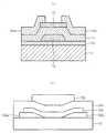
図1(a)、(b)は、本発明の実施形態による酸化物半導体を含む薄膜トランジスタの構造を示す断面図である。(a)は、ボトムゲート(bottom gate)型薄膜トランジスタを示し、(b)は、トップゲート(top gate)型薄膜トランジスタを示す。 1A and 1B are cross-sectional views illustrating the structure of a thin film transistor including an oxide semiconductor according to an embodiment of the present invention. (A) shows a bottom gate type thin film transistor, and (b) shows a top gate type thin film transistor.
図1(a)を参照すると、本発明の実施形態による酸化物薄膜トランジスタは、基板11の一領域上に形成されたゲート電極13、基板11及びゲート電極13上に形成されたゲート絶縁層14を含んでいる。基板11がSiで形成された場合、Si表面に熱酸化工程による酸化層12をさらに含みうる。
そして、ゲート13に対応するゲート絶縁層14上には、チャンネル15が形成されており、チャンネル15の両側部及びゲート絶縁層14上には、ソース16a及びドレイン16bが形成されている。本発明の実施形態による酸化物薄膜トランジスタは、Zn酸化物又はIn−Zn複合酸化物にTa又はYを添加したチャンネル15を含みうる。Referring to FIG. 1A, an oxide thin film transistor according to an embodiment of the present invention includes a
A
ゲート電極13は、上面及び二つの傾斜した側面を有する構造、例えば、上部の幅が下部幅より狭い台形(trapezoidal)の断面を有するものでありうる。ゲート絶縁層14は、ゲート電極13の上面及び側面と酸化層12の上面の露出面を覆うように形成されたものでありうる。チャンネル15の幅は、ゲート電極13の下面の幅に対応するように、実質的に同一に形成されたものでありうる。 The
図1(b)を参照すると、基板101上に各々形成されたソース102a及びドレイン102bを含み、ソース102a、ドレイン102b間領域に形成されたチャンネル103を備える。チャンネル103及び基板101上には、ゲート絶縁層104が形成されており、チャンネル103に対応するゲート絶縁層104上には、ゲート電極105が形成されている。基板101がSiで形成された場合、基板101の表面には、熱酸化工程による酸化層をさらに含みうる。 Referring to FIG. 1 (b), a
以下、図1(a)、(b)に示す本発明の実施形態による酸化物薄膜トランジスタを形成する各層の形成物質について説明する。
基板11、101は、一般的な半導体素子に使われる基板を使用でき、例えば、Si、ガラスまたは有機物材料を使用しうる。
基板11、101の表面に形成された酸化層12(図2では図示せず)は、例えば、基板11、101がSiで形成された場合、Si基板を熱酸化して形成されたSiO2である。Hereinafter, materials for forming each layer forming the oxide thin film transistor according to the embodiment of the present invention shown in FIGS. 1A and 1B will be described.
As the
The oxide layer 12 (not shown in FIG. 2) formed on the surfaces of the
ゲート電極13、105は、導電性物質を使用でき、例えば、Ti、Pt、Ru、Au、Ag、Mo、Al、W、又はCuのような金属、又はIZO(InZnO)又はAZO(AlZnO)のような金属又は導電性酸化物でありうる。
ゲート絶縁層14、104は、通常の半導体素子に使われる絶縁物質を使用して形成することができる。具体的には、SiO2またはSiO2より誘電率の高いHigh−K物質であるHfO2、Al2O3、Si3N4、又はそれらの混合物を使用することができる。
ソース16a、102a及びドレイン16b、102bは、導電性物質を使用して形成し、例えば、Ti、Pt、Ru、Au、Ag、Mo、Al、W、又はCuのような金属又はIZO(InZnO)又はAZO(AlZnO)のような金属又は導電性酸化物を使用することができる。The
The
The
以下、図2〜図6を参照して、本発明の実施形態による図1で示したボトムゲート型薄膜トランジスタの製造方法について説明する。
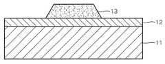
図2を参照すると、まず基板11を用意する。基板11は、Si、ガラス又は有機物材料を使用しうる。Siを基板11として使用する場合、熱酸化工程により基板11の表面に絶縁層12、例えば、SiO2を形成しうる。そして、基板11上を金属または導電性金属酸化物などの導電性物質13aで覆う。Hereinafter, a method of manufacturing the bottom gate type thin film transistor shown in FIG. 1 according to an embodiment of the present invention will be described with reference to FIGS.
Referring to FIG. 2, a
図3を参照すると、導電性物質13aをパターニングすることによって、ゲート13を形成する。
図4を参照すると、ゲート13の上部に絶縁物質を形成してパターニングしてゲート絶縁層14を形成する。ゲート絶縁層は、シリコン酸化物、シリコン窒化物、ハフニウム(Hf)酸化物、アルミニウム酸化物又はハフニウム酸化物及びアルミニウム酸化物の混合物で形成しうる。Referring to FIG. 3, the
Referring to FIG. 4, an insulating material is formed on the
図5を参照すると、ゲート絶縁層14上にチャンネル物質をPVD、CVD又はALDなどの工程で塗布した後、ゲート13に対応するゲート絶縁層14上にチャンネル物質が残留するようにパターニングすることによって、チャンネル15を形成する。
本発明の実施形態では、チャンネル15は、Zn酸化物又はIn−Zn複合酸化物に、Ta又はYのうち、少なくとも1つの物質を添加して形成しうる。Referring to FIG. 5, a channel material is applied on the
In the embodiment of the present invention, the
具体的には、スパッタリング(sputtering)工程でチャンネル15を形成する場合、ZnO又はInZnOで形成されたターゲット(target)とTa又はYで形成されたターゲットとを工程チャンバ内に装着してコ・スパッタリング(co−sputtering)工程でチャンネル15を形成する。また、ZnO又はInZnOに、Ta又はYのうち、少なくとも1つの物質をさらに含む単一ターゲットを使用することも可である。 Specifically, when the
図6を参照すると、金属又は導電性金属酸化物などの物質でチャンネル15及びゲート絶縁層14上を覆った後、チャンネル15の両側部に接続するようにパターニングすることによって、ソース16a及びドレイン16bを形成する。
最後に、400℃以下、例えば、300℃の温度で一般的なファーネス、RTA(rapid thermal annealing)、レーザー又はホットプレートなどを利用して熱処理工程を実施する。Referring to FIG. 6, after covering the
Finally, a heat treatment process is performed using a general furnace, RTA (rapid thermal annealing), laser, hot plate, or the like at a temperature of 400 ° C. or lower, for example, 300 ° C.
(製造例)
実施形態に係る製造例を図1(a)に示した構造を参照して説明する。
酸化膜12が形成されたシリコン基板11上にゲート電極13として約200nm厚さのMoを形成する。
そして、基板11及びゲート電極13上に200nm厚さのシリコン窒化物をコート(coat)してゲート絶縁層14を形成する。
ゲート電極13に対応するゲート絶縁層14上に酸化物半導体をコートしてチャンネル15を形成する。(Production example)
A manufacturing example according to the embodiment will be described with reference to the structure shown in FIG.
Mo having a thickness of about 200 nm is formed as a
Then, a 200 nm thick silicon nitride is coated on the
A
チャンネル15の形成の具体的な工程を説明すれば、次の通りである。
チャンネル15の形成工程の製造例では、IZOターゲット(In2O3:ZnO=1:2mol%)とTa又はYターゲットとを使用する。それらターゲットをスパッタのチャンバ内に装着させた。蒸着条件は、常温でAr及びO2ガスを95:5の比率で全体ガス圧力を保持し、IZOターゲットにRFpower150Wを印加し、TaターゲットにDCpower25〜40Wを印加し、YターゲットにDCpower15〜35Wを印加した。チャンネルは、約70nmの厚さに形成した。A specific process for forming the
In the manufacturing example of the
ここで、InZnOターゲットの代わりに、ZnOターゲットを使用しても良い。そして、チャンネル15の両側にソース及びドレインをTi/Pt(10/100nm)二重層で形成した。
次に、300〜350℃で1時間熱処理工程を実施した。製造工程時、チャンネルの表面に不純物が形成された場合、例えば、エッチング溶液(水:酢酸:塩酸=80:20:0.1vol%)などを使用して除去しうる。Here, a ZnO target may be used instead of the InZnO target. The source and drain were formed on both sides of the
Next, the heat processing process was implemented at 300-350 degreeC for 1 hour. When impurities are formed on the surface of the channel during the manufacturing process, it can be removed using, for example, an etching solution (water: acetic acid: hydrochloric acid = 80: 20: 0.1 vol%).
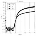
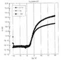
上述したように製造した製造例による酸化物薄膜トランジスタ(チャンネルサイズ:W/L=50μm/4μm)に対して、ソース−ドレイン電圧(0.1V、10V)別のゲート電圧Vg−ドレイン電流Id変化を測定した。With respect to the oxide thin film transistor (channel size: W / L = 50 μm / 4 μm) according to the manufacturing example manufactured as described above, gate voltage Vg -drain current Id according to source-drain voltage (0.1 V, 10 V). Changes were measured.
図7〜図12は、チャンネル物質としてIZOにTaを添加した場合のソース−ドレイン電圧(0.1V、5V、10V)別ゲート電圧Vg−ドレイン電流Idを示すグラフである。
図7〜図12は、スパッタリング工程でTaターゲットの蒸着パワーを各々15W、20W、25W、30W、35W及び40Wに変化させつつ、チャンネル物質を製造した試片のグラフを示す図面である。7 to 12 are graphs showing gate voltage Vg -drain current Id according to source-drain voltages (0.1 V, 5 V, 10 V) when Ta is added to IZO as a channel material.
7 to 12 are graphs showing samples of channel specimens manufactured with channel materials while changing the deposition power of the Ta target to 15 W, 20 W, 25 W, 30 W, 35 W and 40 W, respectively, in the sputtering process.
図7〜図12を参照すると、あらゆる蒸着パワーでトランジスタとして使用可能なトランスファカーブ特性を示すことが分かる。下記の表1では、Taの蒸着パワーによる組成、移動度(mobility)及びスイング電圧(swing voltage)を示す。
酸化物半導体物質に対して組成を評価(evaluate)するために、ICP(Inductively coupled plasma)−AES(Auger Electron Spectroscopy)(誤差範囲約1%)分析を実施した。
表1を参照すると、Taターゲットの蒸着パワーが増加するほど、Taの含量が増加することが分かる。7 to 12, it can be seen that the transfer curve characteristic that can be used as a transistor at any vapor deposition power is shown. Table 1 below shows the composition, mobility, and swing voltage according to the deposition power of Ta.
In order to evaluate the composition of the oxide semiconductor material, ICP (Inductively coupled plasma) -AES (Auger Electron Spectroscopy) (error range about 1%) analysis was performed.
Referring to Table 1, it can be seen that the Ta content increases as the deposition power of the Ta target increases.
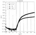
表1に示すTa:In:Znの原子含量(at%)比は、1:2.1〜9.5:1.6〜6.4原子比を示す。特に、Ta15W〜Ta25Wに該当する1:5.7〜9.5:4.8〜6.4原子比の範囲で、On電流が約10−4Aであり、オフ電流が10−11〜10−12A以下であり、オン/オフ電流比は、107以上である特性を示す。
図13及び図14は、Taターゲットの蒸着のためのパワーが25Wでチャンネルを形成した後、300℃で熱処理した試片に対して、50℃にて、経時的にゲート電圧Vg−ドレイン電流Idを測定し、ドレイン電流値が3μAである時のゲート電圧値の変化量を表したグラフである。FIG. 13 and FIG. 14 show the gate voltage Vg -drain current over time at 50 ° C. for a specimen heat-treated at 300 ° C. after forming a channel with a power of 25 W for vapor deposition of Ta target. measured Id, it is a graph showing the variation of the gate voltage value when the drain current value is 3 .mu.A.
図13を参照すると、経時的にゲート電圧値の変化量が少しずつ増加することが分かる。図14を参照すると、約50,000時間が過ぎても、ゲート電圧値の変化量は2.5Vと予想される。したがって、初期の半導体薄膜トランジスタにおいて、初期の電気的な特性の変化量が非常に小さいと判断できる。従って、本発明の実施形態による酸化物薄膜トランジスタは、高いOn/Off電流比と低いOff電流を示し、ヒステリシスがなくて従来の酸化物薄膜トランジスタと比較して改良された特性を有することが分かる。 Referring to FIG. 13, it can be seen that the amount of change in the gate voltage value increases gradually over time. Referring to FIG. 14, even if about 50,000 hours have passed, the amount of change in the gate voltage value is expected to be 2.5V. Therefore, it can be determined that the initial amount of change in electrical characteristics is very small in the initial semiconductor thin film transistor. Accordingly, it can be seen that the oxide thin film transistor according to the embodiment of the present invention has a high On / Off current ratio and a low Off current, and has improved characteristics compared with the conventional oxide thin film transistor without hysteresis.
図15及び図16は、チャンネル物質としてIZOにYを添加した場合のソース−ドレイン電圧(0.1V、5V、10V)別のゲート電圧VGS−ドレイン電流IDSを示すグラフである。図15及び図16は、スパッタリング工程で、Yターゲットの蒸着のためのパワーを各々15Wに保持し、IZOターゲットの蒸着のためのパワーを各々150W及び200Wに保持しつつ、チャンネル物質を製造した試片のグラフである。15 and 16 are graphs showing gate voltage VGS -drain current IDS according to source-drain voltage (0.1 V, 5 V, 10 V) when Y is added to IZO as a channel material. FIGS. 15 and 16 are diagrams illustrating a process for producing a channel material in a sputtering process while maintaining the power for deposition of the Y target at 15 W and maintaining the power for deposition of the IZO target at 150 W and 200 W, respectively. It is a graph of a piece.
図15及び図16を参照すると、チャンネル物質がトランジスタとして好適なトランスファカーブ特性を示すことが分かる。下記の表2では、Yの蒸着のために供給されたパワーに従った原子比を示す。組成を評価するために、ICP(Inductively coupled plasma)−AES(Auger Electron Spectroscopy)(誤差率約1%)分析を実施した。表2を参照すると、Yターゲットの蒸着のためのパワーが増加するほど、チャンネルでのYの含量が増加することが分かる。 Referring to FIGS. 15 and 16, it can be seen that the channel material exhibits a transfer curve characteristic suitable for a transistor. Table 2 below shows the atomic ratio according to the power supplied for Y deposition. In order to evaluate the composition, an ICP (Inductively coupled plasma) -AES (Auger Electron Spectroscopy) (error rate about 1%) analysis was performed. Referring to Table 2, it can be seen that the Y content in the channel increases as the power for Y target deposition increases.
下記の表2で、Y:In:Znの組成比は、1:21.7〜50:14〜41原子比を示す。特に、1:46〜50:30〜41原子比範囲でOn電流が約10−4A、オフ電流が10−11〜10−12A以下であり、オン/オフ電流比は、107以上である特性を示す。
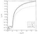
図17は、Yターゲットの蒸着のためのパワーを15Wに保持しつつ、チャンネルを形成した本発明の実施形態による酸化物薄膜トランジスタに対してゲート電圧を0.1、5、10、15、及び20Vで印加する場合のドレイン電圧Vd−ドレイン電流Id値を示すグラフである。FIG. 17 illustrates a gate voltage of 0.1, 5, 10, 15, and 20 V for an oxide thin film transistor according to an embodiment of the present invention in which a channel is formed while maintaining a power for deposition of a Y target at 15 W. 5 is a graph showing the drain voltage Vd -drain current Id value when applied at the same time.
この際、IZO(In2O3:ZnO=1:2mol%)ターゲットには、RF150Wを印加して、コ・スパッタリングした。
図17を参照すると、ゲート電圧を0.1Vで印加する場合、ドレイン電圧が増加しても、ドレイン電流値の変化はないことが分かる。しかし、ゲート電圧を5V以上で印加する場合、ドレイン電圧を増加させれば、ドレイン電流値も徐々に増加することが分かる。At thistime, IZO the(In 2 O 3:: ZnO = 1 2mol%) target by applying a RF150W, and co-sputtering.
Referring to FIG. 17, it can be seen that when the gate voltage is applied at 0.1 V, the drain current value does not change even if the drain voltage increases. However, it can be seen that when the gate voltage is applied at 5 V or higher, the drain current value gradually increases as the drain voltage is increased.
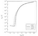
図18及び図19は、Yターゲットの蒸着のためのパワーを15Wを保持しつつ、チャンネルを形成した本発明の実施形態による酸化物薄膜トランジスタを光に露出させた場合の電気的特性の変化を調べるために、ゲート電圧VGS−ドレイン電流IDSを測定した結果を示すグラフである。18 and 19 show changes in electrical characteristics when an oxide thin film transistor according to an embodiment of the present invention in which a channel is formed is exposed to light while maintaining a power for deposition of a Y target of 15 W. Therefore, it is a graph which shows the result of having measured gate voltageVGS -drain currentIDS .
この際、IZO(In2O3:ZnO=1:2mol%)ターゲットには、RF150Wを印加してコ・スパッタリングした。
図18は、ソース−ドレイン電圧が0.1Vである場合であり、図19は、ソース−ドレイン電圧が10Vである場合を示す。ここで、「FIRST」は、試片形成直後を示し、「OPEN」は、試片を自然光に露出させた場合(door open)を示し、「LIGHT」は、薄膜トランジスタに直接ランプ光を照射したものである。At this time, RF150W was applied to the IZO (In2 O3 : ZnO = 1: 2 mol%) target to perform co-sputtering.
18 shows a case where the source-drain voltage is 0.1V, and FIG. 19 shows a case where the source-drain voltage is 10V. Here, “FIRST” indicates immediately after the specimen is formed, “OPEN” indicates the case where the specimen is exposed to natural light (door open), and “LIGHT” indicates that the thin film transistor is directly irradiated with the lamp light. It is.
図18及び図19を参照すると、3つの場合のトランスファカーブの変化が大きくないことがわかる。すなわち、本発明の実施形態による薄膜トランジスタは、外部環境、特に外光に対する変化が少なく、信頼性が優秀であることが分かる。 Referring to FIGS. 18 and 19, it can be seen that the change in the transfer curve in the three cases is not large. That is, it can be seen that the thin film transistor according to the embodiment of the present invention has little change with respect to the external environment, particularly external light, and has excellent reliability.
一方、蒸着された薄膜の組成成分比、IDS−VGSグラフ、移動度特性は、使われるターゲットの種類、蒸着時のターゲット印加電圧、蒸着装備、蒸着圧力、酸素分圧条件、基板温度により変更可能である。
例えば、InZnOターゲット及び、Ta又はYターゲットの2種を使用する場合に代えて、InZnOにTa又はYが含まれた1つのターゲットで使用する場合、蒸着した薄膜組成が変わりうる。On the other hand, the composition ratio, IDS -VGS graph, and mobility characteristics of the deposited thin film depend on the type of target used, target application voltage during deposition, deposition equipment, deposition pressure, oxygen partial pressure conditions, and substrate temperature. It can be changed.
For example, instead of using two types of InZnO target and Ta or Y target, when using one target in which Ta or Y is contained in InZnO, the deposited thin film composition can be changed.
また蒸着した薄膜組成が同じ場合でも、蒸着条件によって薄膜特性の変更が可能である。例えば、スパッタリング工程で酸化物半導体を蒸着する場合、酸素分圧によって酸化物の抵抗範囲は大きく変わりうる。酸素分圧が適量以下に調節される場合、蒸着された薄膜の抵抗が低い薄膜を蒸着し、酸素分圧を高く調節する場合、抵抗が高い薄膜を蒸着しうる。 Even when the deposited thin film composition is the same, the thin film characteristics can be changed depending on the deposition conditions. For example, in the case where an oxide semiconductor is deposited by a sputtering process, the resistance range of the oxide can be significantly changed depending on the oxygen partial pressure. When the oxygen partial pressure is adjusted to an appropriate amount or less, a thin film having a low resistance can be deposited, and when the oxygen partial pressure is adjusted to a high level, a thin film having a high resistance can be deposited.
上述したような実施形態を通じて、当業者ならば、本発明の技術的思想により酸化物半導体を利用してLCD、OLEDなど平板ディスプレイの駆動トランジスタ、メモリ素子の周辺回路構成のためのトランジスタなど多様な電子素子を製造できることは理解されるものである。 Through the above-described embodiments, those skilled in the art can use various oxide semiconductors such as driving transistors for flat panel displays such as LCDs and OLEDs, transistors for peripheral circuit configurations of memory elements, etc. according to the technical idea of the present invention. It is understood that electronic devices can be manufactured.
本発明の実施形態による酸化物薄膜トランジスタは、ボトムゲート型又はトップゲート型として使われうる。結果的に、本発明の範囲は説明した実施形態によって定められるものではなく、特許請求の範囲に記載された技術的思想により定められねばならない。 The oxide thin film transistor according to an embodiment of the present invention may be used as a bottom gate type or a top gate type. As a result, the scope of the present invention is not defined by the described embodiments, but must be defined by the technical ideas described in the claims.
11、101 基板
12 酸化層
13、105 ゲート電極
14、104 ゲート絶縁層
15、103 チャンネル
16a、102a ソース
16b、102b ドレイン
11, 101
Claims (30)
Translated fromJapaneseZn及びTaを含むことを特徴とする酸化物半導体。An oxide semiconductor,
An oxide semiconductor containing Zn and Ta.
ゲートと、
前記ゲートと対応する位置に形成され、Zn及びTaを含む酸化物半導体を有して形成されるチャンネルと、
前記ゲートとチャンネルとの間に形成されるゲート絶縁体と、
前記チャンネルの両側部と各々接触して形成されるソース及びドレインとを備えることを特徴とする酸化物薄膜トランジスタ。An oxide thin film transistor comprising:
The gate,
A channel formed at a position corresponding to the gate and having an oxide semiconductor containing Zn and Ta;
A gate insulator formed between the gate and the channel;
An oxide thin film transistor comprising a source and a drain formed in contact with both sides of the channel.
Zn及びYを含むことを特徴とする酸化物半導体。An oxide semiconductor,
An oxide semiconductor containing Zn and Y.
ゲートと、
前記ゲートと対応する位置に形成され、Zn及びYを含む酸化物半導体を有して形成されるチャンネルと、
前記ゲートとチャンネルとの間に形成されるゲート絶縁体と、
前記チャンネルの両側部と各々接触して形成されるソース及びドレインとを備えることを特徴とする酸化物薄膜トランジスタ。An oxide thin film transistor comprising:
The gate,
A channel formed at a position corresponding to the gate and having an oxide semiconductor containing Zn and Y;
A gate insulator formed between the gate and the channel;
An oxide thin film transistor comprising a source and a drain formed in contact with both sides of the channel.
Znと、Ta又はYの内の少なくとも1つを含むことを特徴とする酸化物半導体。An oxide semiconductor,
An oxide semiconductor comprising Zn and at least one of Ta or Y.
ゲートと、
前記ゲートと対応する位置に形成され、Znと、Ta又はYの内の少なくとも1つを含む酸化物半導体を有して形成されるチャンネルと、
前記ゲートとチャンネルとの間に形成されるゲート絶縁体と、
前記チャンネルの両側部と各々接触して形成されるソース及びドレインとを備えることを特徴とする酸化物薄膜トランジスタ。
An oxide thin film transistor comprising:
The gate,
A channel formed at a position corresponding to the gate and formed of an oxide semiconductor containing Zn and at least one of Ta and Y;
A gate insulator formed between the gate and the channel;
An oxide thin film transistor comprising a source and a drain formed in contact with both sides of the channel.
Applications Claiming Priority (3)
| Application Number | Priority Date | Filing Date | Title |
|---|---|---|---|
| KR1020070060053AKR20080111736A (en) | 2007-06-19 | 2007-06-19 | Oxide semiconductor and thin film transistor comprising the same |
| KR1020080050994AKR101519480B1 (en) | 2008-05-30 | 2008-05-30 | Oxide Semiconductor and Thin Film Transistor comprising the same |
| PCT/KR2008/003471WO2008156312A2 (en) | 2007-06-19 | 2008-06-19 | Oxide semiconductors and thin film transistors comprising the same |
Publications (1)
| Publication Number | Publication Date |
|---|---|
| JP2010530634Atrue JP2010530634A (en) | 2010-09-09 |
Family
ID=40135524
Family Applications (1)
| Application Number | Title | Priority Date | Filing Date |
|---|---|---|---|
| JP2010513115APendingJP2010530634A (en) | 2007-06-19 | 2008-06-19 | Oxide semiconductor and thin film transistor including the same |
Country Status (5)
| Country | Link |
|---|---|
| US (1) | US8450732B2 (en) |
| EP (1) | EP2158608A4 (en) |
| JP (1) | JP2010530634A (en) |
| CN (1) | CN101681925B (en) |
| WO (1) | WO2008156312A2 (en) |
Cited By (7)
| Publication number | Priority date | Publication date | Assignee | Title |
|---|---|---|---|---|
| JP2013055329A (en)* | 2011-08-05 | 2013-03-21 | Semiconductor Energy Lab Co Ltd | Semiconductor device |
| JP2013070052A (en)* | 2011-09-22 | 2013-04-18 | Samsung Display Co Ltd | Oxide semiconductor, thin film transistor including the same, and thin film transistor display panel |
| JP2015165587A (en)* | 2009-11-20 | 2015-09-17 | 株式会社半導体エネルギー研究所 | Semiconductor device |
| JP2016189492A (en)* | 2010-06-25 | 2016-11-04 | 株式会社半導体エネルギー研究所 | Semiconductor device |
| JP2019054287A (en)* | 2010-12-17 | 2019-04-04 | 株式会社半導体エネルギー研究所 | Method for manufacturing transistor |
| JP2020016889A (en)* | 2009-10-16 | 2020-01-30 | 株式会社半導体エネルギー研究所 | Display device |
| JPWO2023145498A1 (en)* | 2022-01-31 | 2023-08-03 |
Families Citing this family (26)
| Publication number | Priority date | Publication date | Assignee | Title |
|---|---|---|---|---|
| KR100785038B1 (en)* | 2006-04-17 | 2007-12-12 | 삼성전자주식회사 | Amorphous ZnO based Thin Film Transistor |
| KR101509663B1 (en) | 2007-02-16 | 2015-04-06 | 삼성전자주식회사 | Method of forming oxide semiconductor layer and method of manufacturing semiconductor device using the same |
| KR101334181B1 (en)* | 2007-04-20 | 2013-11-28 | 삼성전자주식회사 | Thin Film Transistor having selectively crystallized channel layer and method of manufacturing the same |
| JP2010530634A (en) | 2007-06-19 | 2010-09-09 | サムスン エレクトロニクス カンパニー リミテッド | Oxide semiconductor and thin film transistor including the same |
| US7935964B2 (en)* | 2007-06-19 | 2011-05-03 | Samsung Electronics Co., Ltd. | Oxide semiconductors and thin film transistors comprising the same |
| KR101496148B1 (en)* | 2008-05-15 | 2015-02-27 | 삼성전자주식회사 | Semiconductor device and manufacturing method thereof |
| KR101468591B1 (en)* | 2008-05-29 | 2014-12-04 | 삼성전자주식회사 | Oxide semiconductor and thin film transistor comprising the same |
| KR100993416B1 (en)* | 2009-01-20 | 2010-11-09 | 삼성모바일디스플레이주식회사 | A flat panel display comprising a thin film transistor, a method of manufacturing the same, and a thin film transistor |
| US8378342B2 (en)* | 2009-03-23 | 2013-02-19 | Samsung Electronics Co., Ltd. | Oxide semiconductor and thin film transistor including the same |
| WO2011037050A1 (en) | 2009-09-24 | 2011-03-31 | Semiconductor Energy Laboratory Co., Ltd. | Semiconductor device and manufacturing method thereof |
| KR20220127372A (en) | 2009-09-24 | 2022-09-19 | 가부시키가이샤 한도오따이 에네루기 켄큐쇼 | Oxide semiconductor film and semiconductor device |
| KR101113370B1 (en)* | 2009-11-11 | 2012-02-29 | 삼성모바일디스플레이주식회사 | Thin Film Transistor and Organic Light Emitting Display device using thereof |
| KR102241766B1 (en) | 2009-12-04 | 2021-04-19 | 가부시키가이샤 한도오따이 에네루기 켄큐쇼 | Semiconductor device and manufacturing method thereof |
| KR20130009978A (en)* | 2010-02-26 | 2013-01-24 | 가부시키가이샤 한도오따이 에네루기 켄큐쇼 | Method for manufacturing semiconductor element and deposition apparatus |
| US9564531B2 (en) | 2010-03-22 | 2017-02-07 | Samsung Electronics Co., Ltd. | Thin film transistors, methods of manufacturing thin film transistors, and semiconductor device including thin film transistors |
| US9443984B2 (en) | 2010-12-28 | 2016-09-13 | Semiconductor Energy Laboratory Co., Ltd. | Semiconductor device and manufacturing method thereof |
| US20130270109A1 (en)* | 2010-12-28 | 2013-10-17 | Kabushiki Kaisha Kobe Seiko Sho (Kobe Steel, Ltd.) | Oxide for semiconductor layer of thin-film transistor, sputtering target, and thin-film transistor |
| KR20140003315A (en) | 2011-06-08 | 2014-01-09 | 가부시키가이샤 한도오따이 에네루기 켄큐쇼 | Sputtering target, method for manufacturing sputtering target, and method for forming thin film |
| CN102403363A (en)* | 2011-10-27 | 2012-04-04 | 华南理工大学 | Double-layered oxide thin film transistor and preparation method thereof |
| CN102420289A (en)* | 2011-10-28 | 2012-04-18 | 华南理工大学 | Tantalum-doped oxide semiconductor material and preparation method and application thereof |
| US8829528B2 (en)* | 2011-11-25 | 2014-09-09 | Semiconductor Energy Laboratory Co., Ltd. | Semiconductor device including groove portion extending beyond pixel electrode |
| KR20230004930A (en) | 2012-04-13 | 2023-01-06 | 가부시키가이샤 한도오따이 에네루기 켄큐쇼 | Semiconductor device |
| CN102832235A (en)* | 2012-09-14 | 2012-12-19 | 华南理工大学 | Oxide semiconductor and method for manufacturing same |
| WO2014073585A1 (en)* | 2012-11-08 | 2014-05-15 | Semiconductor Energy Laboratory Co., Ltd. | Metal oxide film and method for forming metal oxide film |
| CN103022152A (en)* | 2012-12-26 | 2013-04-03 | 青岛盛嘉信息科技有限公司 | Thin film transistor |
| TW201812419A (en)* | 2016-07-25 | 2018-04-01 | 半導體能源研究所股份有限公司 | Method and device for manufacturing transistor |
Citations (2)
| Publication number | Priority date | Publication date | Assignee | Title |
|---|---|---|---|---|
| JP2005093974A (en)* | 2003-09-18 | 2005-04-07 | Ind Technol Res Inst | Semiconductor material of thin film transistor element active layer and manufacturing method thereof |
| WO2007040194A1 (en)* | 2005-10-05 | 2007-04-12 | Idemitsu Kosan Co., Ltd. | Tft substrate and method for manufacturing tft substrate |
Family Cites Families (84)
| Publication number | Priority date | Publication date | Assignee | Title |
|---|---|---|---|---|
| US4960718A (en) | 1985-12-13 | 1990-10-02 | Allied-Signal Inc. | MESFET device having a semiconductor surface barrier layer |
| JPH0244263B2 (en) | 1987-04-22 | 1990-10-03 | Kagaku Gijutsucho Mukizaishitsu Kenkyushocho | INGAZN7O10DESHIMESARERUROTSUHOSHOKEINOSOJOKOZOOJUSURUKAGOBUTSUOYOBISONOSEIZOHO |
| JP3124101B2 (en) | 1992-01-30 | 2001-01-15 | ローム株式会社 | Nonvolatile semiconductor memory device and method of manufacturing the same |
| KR950002052B1 (en) | 1992-10-30 | 1995-03-10 | 신하성 | Pretreatment Chemical Nickel Plating Method for Copper Plating Homica Sheets |
| CA2150724A1 (en) | 1992-12-15 | 1994-06-23 | Akira Kaijou | Transparent electrically conductive layer, electrically conductive transparent substrate and electrically conductive material |
| JP3246189B2 (en) | 1994-06-28 | 2002-01-15 | 株式会社日立製作所 | Semiconductor display device |
| US5548132A (en) | 1994-10-24 | 1996-08-20 | Micron Technology, Inc. | Thin film transistor with large grain size DRW offset region and small grain size source and drain and channel regions |
| US5532180A (en) | 1995-06-02 | 1996-07-02 | Ois Optical Imaging Systems, Inc. | Method of fabricating a TFT with reduced channel length |
| JPH10306367A (en) | 1997-05-06 | 1998-11-17 | Sumitomo Metal Mining Co Ltd | ZnO-Ga2O3-based sintered body for sputtering target and method for producing the same |
| IL125604A (en) | 1997-07-30 | 2004-03-28 | Saifun Semiconductors Ltd | Non-volatile electrically erasable and programmble semiconductor memory cell utilizing asymmetrical charge |
| JP3884564B2 (en) | 1998-05-20 | 2007-02-21 | 出光興産株式会社 | Organic EL light emitting device and light emitting device using the same |
| US6338987B1 (en) | 1998-08-27 | 2002-01-15 | Lg.Philips Lcd Co., Ltd. | Method for forming polycrystalline silicon layer and method for fabricating thin film transistor |
| JP3276930B2 (en) | 1998-11-17 | 2002-04-22 | 科学技術振興事業団 | Transistor and semiconductor device |
| JP3423896B2 (en) | 1999-03-25 | 2003-07-07 | 科学技術振興事業団 | Semiconductor devices |
| KR100317642B1 (en) | 1999-05-27 | 2001-12-22 | 구본준, 론 위라하디락사 | Method for manufacturing a Thin Film Transistor using a metal plating |
| US6998656B2 (en) | 2003-02-07 | 2006-02-14 | Hewlett-Packard Development Company, L.P. | Transparent double-injection field-effect transistor |
| US6882012B2 (en) | 2000-02-28 | 2005-04-19 | Semiconductor Energy Laboratory Co., Ltd. | Semiconductor device and a method of manufacturing the same |
| KR100382955B1 (en) | 2000-10-10 | 2003-05-09 | 엘지.필립스 엘시디 주식회사 | Method for fabricating the array substrate for Liquid crystal display device and the same |
| JP3711857B2 (en) | 2000-10-11 | 2005-11-02 | 株式会社村田製作所 | Semiconductor porcelain composition having negative resistance temperature characteristic and negative characteristic thermistor |
| US6727533B2 (en) | 2000-11-29 | 2004-04-27 | Fujitsu Limited | Semiconductor apparatus having a large-size bus connection |
| KR100766493B1 (en) | 2001-02-12 | 2007-10-15 | 삼성전자주식회사 | Thin Film Transistor Liquid Crystal Display |
| JP2002320848A (en) | 2001-02-23 | 2002-11-05 | Honda Motor Co Ltd | Hydrogen storage material |
| KR20020082637A (en) | 2001-04-25 | 2002-10-31 | 광주과학기술원 | Metal electrode for light emitting diodes using n-ZnO group semiconductor and manufacturing method thereof |
| KR100406442B1 (en) | 2001-05-17 | 2003-11-19 | 한국과학기술연구원 | Wave-length selective multi-layered transparent conducting thin films |
| TW546840B (en) | 2001-07-27 | 2003-08-11 | Hitachi Ltd | Non-volatile semiconductor memory device |
| KR100909315B1 (en) | 2001-08-02 | 2009-07-24 | 이데미쓰 고산 가부시키가이샤 | Sputtering Target, Transparent Conductive Film and Manufacturing Method Thereof |
| JP4090716B2 (en) | 2001-09-10 | 2008-05-28 | 雅司 川崎 | Thin film transistor and matrix display device |
| US6562491B1 (en) | 2001-10-15 | 2003-05-13 | Advanced Micro Devices, Inc. | Preparation of composite high-K dielectrics |
| WO2003040441A1 (en) | 2001-11-05 | 2003-05-15 | Japan Science And Technology Agency | Natural superlattice homologous single crystal thin film, method for preparation thereof, and device using said single crystal thin film |
| CN1445821A (en) | 2002-03-15 | 2003-10-01 | 三洋电机株式会社 | Forming method of ZnO film and ZnO semiconductor layer, semiconductor element and manufacturing method thereof |
| US7189992B2 (en) | 2002-05-21 | 2007-03-13 | State Of Oregon Acting By And Through The Oregon State Board Of Higher Education On Behalf Of Oregon State University | Transistor structures having a transparent channel |
| US6929970B2 (en) | 2002-09-12 | 2005-08-16 | Agfa-Gevaert | Process for preparing nano-porous metal oxide semiconductor layers |
| US7067843B2 (en) | 2002-10-11 | 2006-06-27 | E. I. Du Pont De Nemours And Company | Transparent oxide semiconductor thin film transistors |
| US6858899B2 (en) | 2002-10-15 | 2005-02-22 | Matrix Semiconductor, Inc. | Thin film transistor with metal oxide layer and method of making same |
| EP1574596A1 (en) | 2002-12-18 | 2005-09-14 | Sony Chemicals Corp. | Transparent conductive film and film forming method therefor |
| JP4222078B2 (en) | 2003-03-26 | 2009-02-12 | ブラザー工業株式会社 | Recording device |
| JP4212413B2 (en) | 2003-05-27 | 2009-01-21 | シャープ株式会社 | Oxide semiconductor light emitting device |
| JP4598673B2 (en)* | 2003-06-13 | 2010-12-15 | パナソニック株式会社 | Light emitting element and display device |
| JP4108633B2 (en) | 2003-06-20 | 2008-06-25 | シャープ株式会社 | THIN FILM TRANSISTOR, MANUFACTURING METHOD THEREOF, AND ELECTRONIC DEVICE |
| JP2005026465A (en) | 2003-07-02 | 2005-01-27 | Sharp Corp | Oxide semiconductor light emitting device |
| US20050017244A1 (en) | 2003-07-25 | 2005-01-27 | Randy Hoffman | Semiconductor device |
| US7262463B2 (en) | 2003-07-25 | 2007-08-28 | Hewlett-Packard Development Company, L.P. | Transistor including a deposited channel region having a doped portion |
| US7071122B2 (en)* | 2003-12-10 | 2006-07-04 | International Business Machines Corporation | Field effect transistor with etched-back gate dielectric |
| US7220635B2 (en) | 2003-12-19 | 2007-05-22 | Intel Corporation | Method for making a semiconductor device with a metal gate electrode that is formed on an annealed high-k gate dielectric layer |
| JP2005223102A (en) | 2004-02-04 | 2005-08-18 | Nec Corp | Nonvolatile memory device and manufacturing method thereof |
| CN1998087B (en) | 2004-03-12 | 2014-12-31 | 独立行政法人科学技术振兴机构 | Amorphous oxide and thin film transistor |
| US7297977B2 (en) | 2004-03-12 | 2007-11-20 | Hewlett-Packard Development Company, L.P. | Semiconductor device |
| US7145174B2 (en) | 2004-03-12 | 2006-12-05 | Hewlett-Packard Development Company, Lp. | Semiconductor device |
| US7211825B2 (en) | 2004-06-14 | 2007-05-01 | Yi-Chi Shih | Indium oxide-based thin film transistors and circuits |
| JP2006005116A (en) | 2004-06-17 | 2006-01-05 | Casio Comput Co Ltd | Film forming method, semiconductor film, and laminated insulating film |
| KR100560796B1 (en) | 2004-06-24 | 2006-03-13 | 삼성에스디아이 주식회사 | Organic thin film transistor and its manufacturing method |
| US20060003485A1 (en) | 2004-06-30 | 2006-01-05 | Hoffman Randy L | Devices and methods of making the same |
| US7378286B2 (en) | 2004-08-20 | 2008-05-27 | Sharp Laboratories Of America, Inc. | Semiconductive metal oxide thin film ferroelectric memory transistor |
| US7285501B2 (en)* | 2004-09-17 | 2007-10-23 | Hewlett-Packard Development Company, L.P. | Method of forming a solution processed device |
| JP4158755B2 (en) | 2004-09-30 | 2008-10-01 | セイコーエプソン株式会社 | Method for producing functional film, method for producing thin film transistor |
| US7382421B2 (en) | 2004-10-12 | 2008-06-03 | Hewlett-Packard Development Company, L.P. | Thin film transistor with a passivation layer |
| US7374984B2 (en)* | 2004-10-29 | 2008-05-20 | Randy Hoffman | Method of forming a thin film component |
| US7298084B2 (en) | 2004-11-02 | 2007-11-20 | 3M Innovative Properties Company | Methods and displays utilizing integrated zinc oxide row and column drivers in conjunction with organic light emitting diodes |
| US7791072B2 (en) | 2004-11-10 | 2010-09-07 | Canon Kabushiki Kaisha | Display |
| US7863611B2 (en) | 2004-11-10 | 2011-01-04 | Canon Kabushiki Kaisha | Integrated circuits utilizing amorphous oxides |
| KR100953596B1 (en) | 2004-11-10 | 2010-04-21 | 캐논 가부시끼가이샤 | Light emitting device |
| US7829444B2 (en) | 2004-11-10 | 2010-11-09 | Canon Kabushiki Kaisha | Field effect transistor manufacturing method |
| AU2005302964B2 (en) | 2004-11-10 | 2010-11-04 | Canon Kabushiki Kaisha | Field effect transistor employing an amorphous oxide |
| EP2453481B1 (en) | 2004-11-10 | 2017-01-11 | Canon Kabushiki Kaisha | Field effect transistor with amorphous oxide |
| US7453065B2 (en) | 2004-11-10 | 2008-11-18 | Canon Kabushiki Kaisha | Sensor and image pickup device |
| KR100688521B1 (en) | 2005-01-18 | 2007-03-02 | 삼성전자주식회사 | Semiconductor device including high dielectric constant insulating film and manufacturing method thereof |
| US20060220023A1 (en)* | 2005-03-03 | 2006-10-05 | Randy Hoffman | Thin-film device |
| US8030643B2 (en) | 2005-03-28 | 2011-10-04 | Semiconductor Energy Laboratory Co., Ltd. | Memory device and manufacturing method the same |
| KR100667043B1 (en) | 2005-04-29 | 2007-01-10 | (주) 세라컴 | Zinc oxide single crystal thin film manufacturing method |
| JP2006344849A (en) | 2005-06-10 | 2006-12-21 | Casio Comput Co Ltd | Thin film transistor |
| US7402506B2 (en) | 2005-06-16 | 2008-07-22 | Eastman Kodak Company | Methods of making thin film transistors comprising zinc-oxide-based semiconductor materials and transistors made thereby |
| US7507618B2 (en) | 2005-06-27 | 2009-03-24 | 3M Innovative Properties Company | Method for making electronic devices using metal oxide nanoparticles |
| JP5058469B2 (en) | 2005-09-06 | 2012-10-24 | キヤノン株式会社 | Sputtering target and method for forming a thin film using the target |
| EP1770788A3 (en) | 2005-09-29 | 2011-09-21 | Semiconductor Energy Laboratory Co., Ltd. | Semiconductor device having oxide semiconductor layer and manufacturing method thereof |
| US8679587B2 (en) | 2005-11-29 | 2014-03-25 | State of Oregon acting by and through the State Board of Higher Education action on Behalf of Oregon State University | Solution deposition of inorganic materials and electronic devices made comprising the inorganic materials |
| US7576394B2 (en) | 2006-02-02 | 2009-08-18 | Kochi Industrial Promotion Center | Thin film transistor including low resistance conductive thin films and manufacturing method thereof |
| JP5110803B2 (en) | 2006-03-17 | 2012-12-26 | キヤノン株式会社 | FIELD EFFECT TRANSISTOR USING OXIDE FILM FOR CHANNEL AND METHOD FOR MANUFACTURING THE SAME |
| US20070254399A1 (en) | 2006-04-27 | 2007-11-01 | Industrial Technology Research Institute | Low temperature direct deposited polycrystalline silicon thin film transistor structure and method for manufacturing the same |
| JP4332545B2 (en) | 2006-09-15 | 2009-09-16 | キヤノン株式会社 | Field effect transistor and manufacturing method thereof |
| KR100811997B1 (en) | 2006-12-04 | 2008-03-10 | 삼성에스디아이 주식회사 | Thin film transistor and its manufacturing method and flat panel display device including the same |
| KR101509663B1 (en) | 2007-02-16 | 2015-04-06 | 삼성전자주식회사 | Method of forming oxide semiconductor layer and method of manufacturing semiconductor device using the same |
| JP2010530634A (en) | 2007-06-19 | 2010-09-09 | サムスン エレクトロニクス カンパニー リミテッド | Oxide semiconductor and thin film transistor including the same |
| US7935964B2 (en) | 2007-06-19 | 2011-05-03 | Samsung Electronics Co., Ltd. | Oxide semiconductors and thin film transistors comprising the same |
| JP5322787B2 (en) | 2009-06-11 | 2013-10-23 | 富士フイルム株式会社 | THIN FILM TRANSISTOR AND MANUFACTURING METHOD THEREOF, ELECTRO-OPTICAL DEVICE, AND SENSOR |
- 2008
- 2008-06-19JPJP2010513115Apatent/JP2010530634A/enactivePending
- 2008-06-19CNCN2008800212830Apatent/CN101681925B/ennot_activeExpired - Fee Related
- 2008-06-19EPEP08766432Apatent/EP2158608A4/ennot_activeWithdrawn
- 2008-06-19WOPCT/KR2008/003471patent/WO2008156312A2/ennot_activeCeased
- 2008-06-19USUS12/213,402patent/US8450732B2/ennot_activeExpired - Fee Related
Patent Citations (2)
| Publication number | Priority date | Publication date | Assignee | Title |
|---|---|---|---|---|
| JP2005093974A (en)* | 2003-09-18 | 2005-04-07 | Ind Technol Res Inst | Semiconductor material of thin film transistor element active layer and manufacturing method thereof |
| WO2007040194A1 (en)* | 2005-10-05 | 2007-04-12 | Idemitsu Kosan Co., Ltd. | Tft substrate and method for manufacturing tft substrate |
Cited By (18)
| Publication number | Priority date | Publication date | Assignee | Title |
|---|---|---|---|---|
| JP2020016889A (en)* | 2009-10-16 | 2020-01-30 | 株式会社半導体エネルギー研究所 | Display device |
| US12170338B2 (en) | 2009-10-16 | 2024-12-17 | Semiconductor Energy Laboratory Co., Ltd. | Logic circuit and semiconductor device |
| US11742432B2 (en) | 2009-10-16 | 2023-08-29 | Semiconductor Energy Laboratory Co., Ltd. | Logic circuit and semiconductor device |
| US11302824B2 (en) | 2009-10-16 | 2022-04-12 | Semiconductor Energy Laboratory Co., Ltd. | Logic circuit and semiconductor device |
| JP2015165587A (en)* | 2009-11-20 | 2015-09-17 | 株式会社半導体エネルギー研究所 | Semiconductor device |
| US9748401B2 (en) | 2010-06-25 | 2017-08-29 | Semiconductor Energy Laboratory Co., Ltd. | Transistor and semiconductor device |
| JP2016189492A (en)* | 2010-06-25 | 2016-11-04 | 株式会社半導体エネルギー研究所 | Semiconductor device |
| JP2019054287A (en)* | 2010-12-17 | 2019-04-04 | 株式会社半導体エネルギー研究所 | Method for manufacturing transistor |
| US11049977B2 (en) | 2010-12-17 | 2021-06-29 | Semiconductor Energy Laboratory Co., Ltd. | Oxide material and semiconductor device |
| US11217702B2 (en) | 2010-12-17 | 2022-01-04 | Semiconductor Energy Laboratory Co., Ltd. | Oxide material and semiconductor device |
| US11688810B2 (en) | 2010-12-17 | 2023-06-27 | Semiconductor Energy Laboratory Co., Ltd. | Oxide material and semiconductor device |
| US12057510B2 (en) | 2010-12-17 | 2024-08-06 | Semiconductor Energy Laboratory Co., Ltd. | Oxide material and semiconductor device |
| US12396216B2 (en) | 2010-12-17 | 2025-08-19 | Semiconductor Energy Laboratory Co., Ltd. | Oxide material and semiconductor device |
| JP2013055329A (en)* | 2011-08-05 | 2013-03-21 | Semiconductor Energy Lab Co Ltd | Semiconductor device |
| JP2013070052A (en)* | 2011-09-22 | 2013-04-18 | Samsung Display Co Ltd | Oxide semiconductor, thin film transistor including the same, and thin film transistor display panel |
| JPWO2023145498A1 (en)* | 2022-01-31 | 2023-08-03 | ||
| JP7422269B2 (en) | 2022-01-31 | 2024-01-25 | 三井金属鉱業株式会社 | Sputtering target material and method for producing oxide semiconductor |
| TWI850971B (en)* | 2022-01-31 | 2024-08-01 | 日商三井金屬鑛業股份有限公司 | Sputtering target and method for manufacturing oxide semiconductor |
Also Published As
| Publication number | Publication date |
|---|---|
| EP2158608A4 (en) | 2010-07-14 |
| CN101681925A (en) | 2010-03-24 |
| WO2008156312A2 (en) | 2008-12-24 |
| EP2158608A2 (en) | 2010-03-03 |
| CN101681925B (en) | 2011-11-30 |
| WO2008156312A3 (en) | 2009-02-12 |
| US20080315194A1 (en) | 2008-12-25 |
| US8450732B2 (en) | 2013-05-28 |
Similar Documents
| Publication | Publication Date | Title |
|---|---|---|
| JP2010530634A (en) | Oxide semiconductor and thin film transistor including the same | |
| JP5526023B2 (en) | Oxide semiconductor and thin film transistor including the same | |
| KR101468591B1 (en) | Oxide semiconductor and thin film transistor comprising the same | |
| KR101468594B1 (en) | Oxide semiconductor and thin film transistor including the same | |
| KR101552975B1 (en) | Oxide semiconductor and thin film transistor including the same | |
| US8378342B2 (en) | Oxide semiconductor and thin film transistor including the same | |
| KR101496150B1 (en) | Oxide Semiconductor and Thin Film Transistor comprising the same | |
| KR20090002841A (en) | Oxide semiconductor, thin film transistor comprising same, and method of manufacturing | |
| KR101468590B1 (en) | Oxide semiconductor and thin film transistor including the same | |
| CN103545377B (en) | A kind of oxide thin film transistor and manufacture method thereof | |
| KR101519480B1 (en) | Oxide Semiconductor and Thin Film Transistor comprising the same | |
| KR101600051B1 (en) | Oxide Semiconductor and Thin Film Transistor comprising the same | |
| KR20080111736A (en) | Oxide semiconductor and thin film transistor comprising the same | |
| JP2012248883A (en) | Display device manufactured using oxide semiconductor and method for manufacturing the same | |
| KR20150079274A (en) | Thin Film Transistor and Method of manufacturing the same | |
| CN115966469A (en) | Low-temperature low-cost homogeneous double-semiconductor-layer thin film transistor and preparation method thereof | |
| KR20140050993A (en) | Zn compound semiconductor and thin film transistor comprising the same |
Legal Events
| Date | Code | Title | Description |
|---|---|---|---|
| A131 | Notification of reasons for refusal | Free format text:JAPANESE INTERMEDIATE CODE: A131 Effective date:20121120 | |
| A521 | Request for written amendment filed | Free format text:JAPANESE INTERMEDIATE CODE: A523 Effective date:20130220 | |
| A131 | Notification of reasons for refusal | Free format text:JAPANESE INTERMEDIATE CODE: A131 Effective date:20130723 | |
| A02 | Decision of refusal | Free format text:JAPANESE INTERMEDIATE CODE: A02 Effective date:20131217 |