JP2010528478A - Printed circuit and method for making a printed circuit - Google Patents
Printed circuit and method for making a printed circuitDownload PDFInfo
- Publication number
- JP2010528478A JP2010528478AJP2010509531AJP2010509531AJP2010528478AJP 2010528478 AJP2010528478 AJP 2010528478AJP 2010509531 AJP2010509531 AJP 2010509531AJP 2010509531 AJP2010509531 AJP 2010509531AJP 2010528478 AJP2010528478 AJP 2010528478A
- Authority
- JP
- Japan
- Prior art keywords
- substrate
- printed circuit
- metallized
- polytetrafluoroethylene
- image
- Prior art date
- Legal status (The legal status is an assumption and is not a legal conclusion. Google has not performed a legal analysis and makes no representation as to the accuracy of the status listed.)
- Pending
Links
Images


Classifications
- H—ELECTRICITY
- H05—ELECTRIC TECHNIQUES NOT OTHERWISE PROVIDED FOR
- H05K—PRINTED CIRCUITS; CASINGS OR CONSTRUCTIONAL DETAILS OF ELECTRIC APPARATUS; MANUFACTURE OF ASSEMBLAGES OF ELECTRICAL COMPONENTS
- H05K3/00—Apparatus or processes for manufacturing printed circuits
- H05K3/0073—Masks not provided for in groups H05K3/02 - H05K3/46, e.g. for photomechanical production of patterned surfaces
- H05K3/0082—Masks not provided for in groups H05K3/02 - H05K3/46, e.g. for photomechanical production of patterned surfaces characterised by the exposure method of radiation-sensitive masks
- H—ELECTRICITY
- H05—ELECTRIC TECHNIQUES NOT OTHERWISE PROVIDED FOR
- H05K—PRINTED CIRCUITS; CASINGS OR CONSTRUCTIONAL DETAILS OF ELECTRIC APPARATUS; MANUFACTURE OF ASSEMBLAGES OF ELECTRICAL COMPONENTS
- H05K3/00—Apparatus or processes for manufacturing printed circuits
- H05K3/10—Apparatus or processes for manufacturing printed circuits in which conductive material is applied to the insulating support in such a manner as to form the desired conductive pattern
- H05K3/105—Apparatus or processes for manufacturing printed circuits in which conductive material is applied to the insulating support in such a manner as to form the desired conductive pattern by conversion of non-conductive material on or in the support into conductive material, e.g. by using an energy beam
- H05K3/106—Apparatus or processes for manufacturing printed circuits in which conductive material is applied to the insulating support in such a manner as to form the desired conductive pattern by conversion of non-conductive material on or in the support into conductive material, e.g. by using an energy beam by photographic methods
- H—ELECTRICITY
- H05—ELECTRIC TECHNIQUES NOT OTHERWISE PROVIDED FOR
- H05K—PRINTED CIRCUITS; CASINGS OR CONSTRUCTIONAL DETAILS OF ELECTRIC APPARATUS; MANUFACTURE OF ASSEMBLAGES OF ELECTRICAL COMPONENTS
- H05K2203/00—Indexing scheme relating to apparatus or processes for manufacturing printed circuits covered by H05K3/00
- H05K2203/10—Using electric, magnetic and electromagnetic fields; Using laser light
- H05K2203/107—Using laser light
- H—ELECTRICITY
- H05—ELECTRIC TECHNIQUES NOT OTHERWISE PROVIDED FOR
- H05K—PRINTED CIRCUITS; CASINGS OR CONSTRUCTIONAL DETAILS OF ELECTRIC APPARATUS; MANUFACTURE OF ASSEMBLAGES OF ELECTRICAL COMPONENTS
- H05K3/00—Apparatus or processes for manufacturing printed circuits
- H05K3/10—Apparatus or processes for manufacturing printed circuits in which conductive material is applied to the insulating support in such a manner as to form the desired conductive pattern
- H05K3/18—Apparatus or processes for manufacturing printed circuits in which conductive material is applied to the insulating support in such a manner as to form the desired conductive pattern using precipitation techniques to apply the conductive material
- H05K3/181—Apparatus or processes for manufacturing printed circuits in which conductive material is applied to the insulating support in such a manner as to form the desired conductive pattern using precipitation techniques to apply the conductive material by electroless plating
- H05K3/182—Apparatus or processes for manufacturing printed circuits in which conductive material is applied to the insulating support in such a manner as to form the desired conductive pattern using precipitation techniques to apply the conductive material by electroless plating characterised by the patterning method
- H05K3/184—Apparatus or processes for manufacturing printed circuits in which conductive material is applied to the insulating support in such a manner as to form the desired conductive pattern using precipitation techniques to apply the conductive material by electroless plating characterised by the patterning method using masks
- Y—GENERAL TAGGING OF NEW TECHNOLOGICAL DEVELOPMENTS; GENERAL TAGGING OF CROSS-SECTIONAL TECHNOLOGIES SPANNING OVER SEVERAL SECTIONS OF THE IPC; TECHNICAL SUBJECTS COVERED BY FORMER USPC CROSS-REFERENCE ART COLLECTIONS [XRACs] AND DIGESTS
- Y10—TECHNICAL SUBJECTS COVERED BY FORMER USPC
- Y10T—TECHNICAL SUBJECTS COVERED BY FORMER US CLASSIFICATION
- Y10T29/00—Metal working
- Y10T29/49—Method of mechanical manufacture
- Y10T29/49002—Electrical device making
- Y10T29/49117—Conductor or circuit manufacturing
- Y10T29/49124—On flat or curved insulated base, e.g., printed circuit, etc.
- Y10T29/49155—Manufacturing circuit on or in base
Landscapes
- Engineering & Computer Science (AREA)
- Manufacturing & Machinery (AREA)
- Microelectronics & Electronic Packaging (AREA)
- Manufacturing Of Printed Circuit Boards (AREA)
- Manufacturing Of Printed Wiring (AREA)
Abstract
Translated fromJapaneseDescription
Translated fromJapanese本発明は、プリント回路基板技術に関し、より具体的には、非メタライズ基板を被覆することと、回路設計の画像を被覆された基板の上に直接的に焼き付けることとを含む、プリント回路を作るための方法に関する。本発明はまた、該方法からもたらされるプリント回路およびプリント回路基板に関する。 The present invention relates to printed circuit board technology and, more particularly, to make a printed circuit that includes coating a non-metallized substrate and printing an image of the circuit design directly onto the coated substrate. Related to the method. The invention also relates to a printed circuit and a printed circuit board resulting from the method.
プリント回路およびプリント回路基板を作るための従来技術のプロセスは、一般に、プリント回路を形成および現像するためのいくつかの他のステップおよびプロセスとともに、所望のプリント回路の画像を作成するために、ハロゲン化銀のポリエステルベースの薄膜を用いる。フォトプロッタは、一般に、回路設計を描画するための媒体としてハロゲン化銀のポリエステル薄膜を用いる機器の一部である。この機器は次いで、その後の処理に用いられて、金属被覆のために回路を描画したり、特に設計された回路をプリントおよびエッチングしたりする。これは、プリントおよびエッチングプロセスまたはめっきおよびエッチングプロセスとして公知である。 Prior art processes for making printed circuits and printed circuit boards are generally halogenated to produce an image of the desired printed circuit, along with some other steps and processes for forming and developing printed circuits. A silver-based polyester-based thin film is used. Photoplotters are generally part of equipment that uses a silver halide polyester film as a medium for drawing circuit designs. This equipment is then used in subsequent processing to draw circuits for metallization and to print and etch specifically designed circuits. This is known as a printing and etching process or a plating and etching process.
プリント回路基板を形成するための従来技術のプロセスの一例は、CAD/CAM設計を作成するステップと、設計に関連するデータをフォトプロッタに送信するステップと、ハロゲン化銀のポリエステル薄膜にフォトプロットするステップと、送信されたデータからの画像を現像するステップと、中間の加工マークを作成するステップと、描画のために基板をスクラブまたはクリーニングするステップと、基板をドライフィルムによって被覆するステップと、基板を設計に従って描画するステップと、画像を現像するステップと、画像をエッチングするステップと、残っているドライフィルムを除去するステップとを含む。この従来技術のプロセスは、いくつかのステップを必要としており、細線画像の描画、現像、およびエッチングにおいて限界を有する。このプロセスによって、細線の描画は、0.003インチまで一貫して実行され得る。ずっと細かな線の描画、例えば0.0025インチまでの細線の描画は、この従来技術のプロセスを用いるときには、問題を生じ、かつ一貫性がない。さらに、積層板は、銅がパネルに付着された状態で購入されなければならず、このタイプの処理は、高速RF用途に対して「損失性」の問題を作り出し得るアンダーカットおよび粗いエッジによる固有の問題を有する。すなわち、このプロセスによって、任意の粗い突起またはアンダーカットは小さなアンテナのように作動し、信号の進行速度が、高周波の印加中に低減されるかまたは失われる。高周波の用途は、平滑な画像と非常に薄い銅とを必要としている。 An example of a prior art process for forming a printed circuit board is to create a CAD / CAM design, send data related to the design to a photoplotter, and photoplot to a silver halide polyester film. Developing an image from the transmitted data; creating an intermediate processing mark; scrubbing or cleaning the substrate for drawing; coating the substrate with a dry film; The method according to the design, developing the image, etching the image, and removing the remaining dry film. This prior art process requires several steps and has limitations in thin line image drawing, development, and etching. By this process, thin line drawing can be performed consistently up to 0.003 inches. Drawing finer lines, for example, drawing fine lines up to 0.0025 inches, is problematic and inconsistent when using this prior art process. In addition, laminates must be purchased with copper attached to the panel, and this type of processing is inherent with undercuts and rough edges that can create "lossy" problems for high-speed RF applications. Have problems. That is, by this process, any rough protrusions or undercuts act like small antennas, and the signal traveling speed is reduced or lost during the application of high frequencies. High frequency applications require smooth images and very thin copper.
従って、従来技術のプロセスにおいて認められた固有の問題を伴うことなく細線描画を容易にするプリント回路およびプリント回路基板を作るための新方式に対するニーズが存在する。さらに、プリント回路およびプリント回路基板を作るための方法が必要であり、該方法は、従来技術のプロセスに用いられるステップの多くを取り除く一方で、0.0002未満の非常に薄い銅を利用して、アンダーカットのない非常に平坦で粗くない表面を有する細線の描画によるプリント回路およびプリント回路基板の作成をなおも可能にする。 Accordingly, there is a need for new systems for making printed circuits and printed circuit boards that facilitate thin line drawing without the inherent problems found in prior art processes. Further, there is a need for a method for making printed circuits and printed circuit boards, which eliminates many of the steps used in prior art processes while utilizing very thin copper less than 0.0002. Still allows the production of printed circuits and printed circuit boards by drawing fine lines with a very flat and rough surface without undercuts.
本発明は、従来技術のプロセスにおいてドライフィルムの描画に用いられる銀塩フィルムの必要性を取り除く、プリント回路およびプリント回路基板を作るための方法を対象にしている。本発明において、プリント回路およびプリント回路基板を作るための方法は、非メタライズ基板を被覆するステップと、回路設計の画像を該被覆された基板上に直接的に焼き付けるステップとを含む。画像基板は次いで、現像され処理されることにより、さらなるドライフィルムのプリント、ドライフィルムの現像およびエッチングプロセスを必要とせずに、結果としてもたらされるプリント回路を作成し得る。 The present invention is directed to a method for making printed circuits and printed circuit boards that obviates the need for silver salt films used to draw dry films in prior art processes. In the present invention, a printed circuit and a method for making a printed circuit board include coating a non-metallized substrate and printing an image of the circuit design directly on the coated substrate. The image substrate can then be developed and processed to create the resulting printed circuit without the need for further dry film printing, dry film development and etching processes.
例示的な一実施形態において、非メタライズ基板は、液晶重合体、ポリイミド、セラミック、充填型(filled)セラミック、ガラス、充填型ポリ四フッ化エチレン、非充填型ポリ四フッ化エチレン、ポリ四フッ化エチレンの織りガラス、およびポリ四フッ化エチレンの不織ガラスであり得、該非メタライズ基板は、被覆され、次いで所望の回路の画像が、該被覆された基板上に直接的に焼き付けられる。 In one exemplary embodiment, the non-metallized substrate is a liquid crystal polymer, polyimide, ceramic, filled ceramic, glass, filled polytetrafluoroethylene, unfilled polytetrafluoroethylene, polytetrafluoroethylene. Woven glass of ethylene halide and non-woven glass of polytetrafluoroethylene, the non-metallized substrate is coated, and then an image of the desired circuit is baked directly onto the coated substrate.
本発明はまた、上記の方法に従って作られるプリント回路を対象にしており、そこでは、プリント回路が、非常に薄い銅による0.00025インチまでの細線画像を含んでいる。 The present invention is also directed to a printed circuit made according to the method described above, where the printed circuit contains a fine line image up to 0.00025 inch with very thin copper.
プリント回路およびプリント回路基板を作るための本発明の別の例示的な方法は、非メタライズの事前加工された基板を提供するステップと、該基板の表面をレーザ描画に適する感光性の化学薬品によって被覆するステップと、該被覆された基板を乾燥するまでベークするステップと、回路網を設計し、該回路網設計に関連するデータをレーザフォトプロッタまたは直接描画プロッタに送信するステップと、描画ステップのための基準として該被覆された基板内の該加工(tooling)を用いて、該回路網設計を該レーザフォトプロッタまたは直接描画プロッタによって該被覆された基板材料の上に直接的に描画するステップと、該描画された基板を1つ以上の化学作用によって現像するステップと、該現像された画像を銅浴によって処理するステップとを含む。 Another exemplary method of the present invention for making printed circuits and printed circuit boards includes the steps of providing a non-metallized pre-fabricated substrate and the surface of the substrate by a photosensitive chemical suitable for laser writing. Coating, baking the coated substrate to dry, designing a network and sending data related to the network design to a laser photoplotter or direct drawing plotter; Drawing the network design directly on the coated substrate material by the laser photoplotter or direct drawing plotter using the tooling in the coated substrate as a reference for Developing the drawn substrate by one or more chemistries; and treating the developed image with a copper bath. And a step of.
上記された非メタライズ基板は、この方法によって用いられ得、該非メタライズ表面を被覆するために用いられる感光性の化学薬品は、硝酸銀ベースの液体、塩化銀ベースのクエン酸および感光性ゼラチン、鉄ベースの材料、クロム銅ベースの材料、クロムニッケルベースの材料、浸漬金材料、パラジウムとともに用いられるプラチナベースの材料を含み得る。 The non-metallized substrate described above can be used by this method, and the photosensitive chemicals used to coat the non-metallized surface include silver nitrate-based liquids, silver chloride-based citric acid and photosensitive gelatin, iron-based Materials, chromium copper based materials, chromium nickel based materials, immersion gold materials, platinum based materials used with palladium.
本発明は、同様な番号が同様な要素を示す、添付の図面とともに以下の本明細書中に記載される。
プリント回路およびプリント回路基板を組み立てるための本発明の方法は概して、非メタライズ基板を提供することと、該非メタライズ基板を被覆することと、回路設計を該被覆された基板上に直接的に描画することとを含む。描画基板は次いで、1つ以上の化学作用によって現像され、プリント回路またはプリント回路基板を作成するために、銅浴にさらすことによって処理され得る。当業者によって理解されるべきは、非メタライズ基板が描画に対して一様である限り、任意のタイプの非メタライズ基板が用いられ得ることである。さらに、当業者が理解することは、多くの感光性化学薬品が、非メタライズ基板の表面を被覆するために用いられ得、そして様々な化学作用が、描画された基板を現像するために用いられ得ることである。 The inventive method for assembling printed circuits and printed circuit boards generally provides a non-metallized substrate, coating the non-metallized substrate, and drawing a circuit design directly on the coated substrate. Including. The drawing substrate can then be developed by one or more chemistries and processed by exposure to a copper bath to create a printed circuit or printed circuit board. It should be understood by those skilled in the art that any type of non-metallized substrate can be used as long as the non-metallized substrate is uniform for drawing. Furthermore, those skilled in the art will appreciate that many photosensitive chemicals can be used to coat the surface of a non-metallized substrate, and various chemistries can be used to develop the drawn substrate. Is to get.
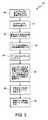
図1は、プリント回路およびプリント回路基板を形成するための従来技術のプロセスを描くフローチャート10を示す。ステップ12において、回路がCAD/CAM設計によって作成され、ステップ14において、回路設計に関連するデータがフォトプロッタに送信される。次に、ステップ16において、回路設計がハロゲン化銀のポリエステル薄膜にフォトプロットされ、ステップ18において、ハロゲン化銀のポリエステル薄膜上の画像が次いで現像される。ステップ20において、中間の加工マークが作成される。ステップ22において、液晶重合体またはポリ四フッ化エチレンなどの基板が次いで、描画に対して基板を準備するためにスクラブまたはクリーニングされる。基板は次いで、ステップ24においてドライフィルムによって被覆され、そしてステップ26において、基板は回路設計に従って描画される。被覆された基板上のプリント回路の描画に続いて、プリント回路の画像が、ステップ28において現像される。被覆された基板上のプリント回路の現像された画像は次いで、ステップ30においてエッチングされ、ステップ32において、あらゆる残りのドライフィルムが、プリント回路を作成するために除去される。 FIG. 1 shows a
ここで図2を参照すると、プリント回路またはプリント回路基板を組み立てるための本発明の方法の例示的な実施形態を描くフローチャート20が示されている。最初に、非メタライズ基板が、ステップ21において被覆される。そしてステップ22において、回路設計が作成される。回路設計に関連するデータは次いで、ステップ24において、フォトプロッタまたは直接描画機器に送信され、そしてステップ26において、回路設計に関連する画像が、被覆された非メタライズ基板の上に直接的にプロットされる。従来技術のプロセスと異なり、画像は、中間のハロゲン化銀のポリエステル薄膜またはジアゾ化合物にはプロットされない。回路設計のプロットされたまたは直接描画された画像は、次いで、ステップ28において現像され、現像された画像は次いで、中間の現像およびエッチングのプロセスを必要とせずに、ステップ30において処理される。 Referring now to FIG. 2, a
プリント回路およびプリント回路基板を組み立てるための本発明の別の、さらに詳細な例示的な実施形態が、図3のフローチャート50によって示されている。最初に、非メタライズの事前加工された基板が、ステップ48において提供され、該基板は次いで、ステップ51において被覆される。非メタライズの事前加工された基板は、描画に対して基板が平坦で、かつ一様である限り、プリント回路基板技術の産業で公知の任意の基板または接合薄膜を含み得る。例えば、非メタライズ基板は、液晶重合体、ポリイミド、平面ガラスプレート、テレフタル酸ポリエチレン、充填型ポリ四フッ化エチレン、非充填型ポリ四フッ化エチレン、ポリ四フッ化エチレンの織りガラス、ポリ四フッ化エチレンの不織ガラス、低温焼結型(cofired)セラミック(LTCC)、および高温焼結型セラミック(HTCC)であり得る。基板は、織りまたは不織りであり、充填型または非充填型セラミックであり得る。さらに、多くの公知の製品がまた非メタライズ基板として用いられ得、それらの製品は、KAPTON、SPEED BOARD C、ULTRALAM、FR4 EPOXIES、MULTIFUNCTIONAL EPOXIES、BT EPOXIES、LCP、およびDUROIDとして公知の製品を含む。非メタライズの事前加工された基板は、ステップ51において、レーザ描画に適する感光性化学薬品によって被覆される。そのような化学薬品は、硝酸銀ベースの液体、塩化銀ベースのクエン酸および感光性ゼラチン、鉄ベースの材料、クロム銅ベースの材料、およびクロムニッケルベースの材料、無電解ニッケル、浸漬金、プラチナベースおよびパラジウムベースの材料を含み得るが、これらに限定されない。 Another more detailed exemplary embodiment of the present invention for assembling printed circuits and printed circuit boards is illustrated by
ステップ49において、被覆された基板は次いで、乾燥するまでベークされる。例示的な一実施形態において、被覆された基板は、従来のオーブンまたはコンベヤオーブンで約20〜30分の間、摂氏40度でベークされる。プリント回路またはプリント回路基板用の回路網が次いで、ステップ52において設計され、そして回路設計に関連するデータが、ステップ54においてフォトプロッタまたはレーザ直接描画に送信される。次に、ステップ56において、回路網設計が、被覆された基板上にフォトプロッタまたはレーザ直接描画器を用いて描画され、被覆された基板内の加工マークが、描画の間の基準ガイドとして用いられる。従来技術のプロセスと対比すると、ハロゲン化銀のポリエステル薄膜は、描画には用いられない。代わりに、被覆された基板が、描画用のフォトプロッタまたはレーザ直接描画器の上に配置される。結果として、プリント回路およびプリント回路基板を組み立てるための本発明の方法は、多くの製品、ステップおよび手順の必要性を取り除き、その取り除かれた製品、ステップおよび手順には、銀塩フィルム、ジアゾフィルム、ドライフィルム、液状ドライフィルム、平行または非平行のUV光源、熱ロール真空積層、標準のプリント回路基板の現像およびエッチングおよび除去、ならびに化学薬品の廃棄物処理の必要性とともに、関連するオーバヘッドならびに直接および間接の人件費を含む。 In
図3に示された例示的な方法において、描画基板は次いで、ステップ58において化学作用により現像される。ここで、KODAK DEKTOLまたはNGS NAT540およびFIXER NAT750のような任意の紙タイプの現像剤などの化学作用が用いられるか、またはEDTAベースの現像剤であり得る。最後に、現像された画像は、結果としてもたらされるプリント回路またはプリント回路基板を作成するために、ステップ60において銅浴によって処理される。これは、当該分野で公知の回路基板ホールの金属被覆に用いられる任意の標準的な無電解銅めっきプロセスを含み得る。 In the exemplary method shown in FIG. 3, the drawing substrate is then chemically developed at
以上の説明は、本発明の好適で例示的な実施形態であり、本発明は、本明細書中に示されまたは記載された特定の形態に限定されないことが理解されるであろう。添付の特許請求の範囲において表現されるような本発明の範囲を逸脱することなく、様々な修正が、本発明を製作し、そして用いるために、本明細書中に開示されたステップの設計、配列、順序、および種類において行われ得る。 It will be understood that the foregoing description is of preferred and exemplary embodiments of the invention and that the invention is not limited to the specific forms shown or described herein. Various modifications may be made to the design of the steps disclosed herein to make and use the invention without departing from the scope of the invention as expressed in the appended claims. It can be done in sequence, order, and type.
Claims (16)
Translated fromJapanese非メタライズ基板を被覆することと、
回路設計の画像を該被覆された基板上に直接的に焼き付けることと
を包含する、方法。A method for making a printed circuit comprising:
Coating a non-metallized substrate;
Printing an image of a circuit design directly onto the coated substrate.
該描画された基板を銅浴にさらすことによって該現像された画像を処理するステップと
をさらに包含する、請求項1に記載の方法。Developing the drawn substrate;
The method of claim 1, further comprising: processing the developed image by exposing the drawn substrate to a copper bath.
非メタライズの事前加工された基板を提供することと、
該基板の表面をレーザ描画に適する感光性の化学薬品によって被覆することと、
該被覆された基板を乾燥するまでベークすることと、
回路網を設計し、該回路網設計に関連するデータをフォトプロッタに送信することと、
描画するステップのための基準として該被覆された基板内の該加工を用いて、該フォトプロッタによって、該回路網設計を該被覆された基板材料の上に直接的に描画することと、
該描画された基板を1つ以上の化学作用によって現像することと、
該現像された画像を銅浴によって処理することと
を包含する、方法。A method for making a printed circuit board, the method comprising:
Providing a non-metallized pre-fabricated substrate;
Coating the surface of the substrate with a photosensitive chemical suitable for laser drawing;
Baking the coated substrate to dryness;
Designing a network and transmitting data related to the network design to a photoplotter;
Drawing the network design directly on the coated substrate material by the photoplotter, using the processing in the coated substrate as a reference for the drawing step;
Developing the drawn substrate by one or more chemistries;
Treating the developed image with a copper bath.
Applications Claiming Priority (2)
| Application Number | Priority Date | Filing Date | Title |
|---|---|---|---|
| US11/751,350US7754417B2 (en) | 2007-05-21 | 2007-05-21 | Printed circuits and method for making same |
| PCT/US2008/064391WO2008144742A1 (en) | 2007-05-21 | 2008-05-21 | Printed circuits and method for making same |
Publications (2)
| Publication Number | Publication Date |
|---|---|
| JP2010528478Atrue JP2010528478A (en) | 2010-08-19 |
| JP2010528478A5 JP2010528478A5 (en) | 2011-07-07 |
Family
ID=40071354
Family Applications (1)
| Application Number | Title | Priority Date | Filing Date |
|---|---|---|---|
| JP2010509531APendingJP2010528478A (en) | 2007-05-21 | 2008-05-21 | Printed circuit and method for making a printed circuit |
Country Status (5)
| Country | Link |
|---|---|
| US (1) | US7754417B2 (en) |
| EP (1) | EP2160758A4 (en) |
| JP (1) | JP2010528478A (en) |
| CN (1) | CN101971309A (en) |
| WO (1) | WO2008144742A1 (en) |
Families Citing this family (4)
| Publication number | Priority date | Publication date | Assignee | Title |
|---|---|---|---|---|
| US8313891B2 (en)* | 2007-05-21 | 2012-11-20 | Vectraone Technologies, Llc | Printed circuits and method for making same |
| KR102623838B1 (en) | 2018-08-20 | 2024-01-11 | 삼성디스플레이 주식회사 | Display device and manufacturing method therof |
| CN112939575A (en)* | 2021-01-29 | 2021-06-11 | 哈尔滨工业大学 | Method for rapidly preparing manganese-cobalt spinel coating by microwave mixing and heating |
| CN115835542A (en)* | 2022-12-29 | 2023-03-21 | 博罗县精汇电子科技有限公司 | Preparation method of multilayer rigid-flex board |
Citations (3)
| Publication number | Priority date | Publication date | Assignee | Title |
|---|---|---|---|---|
| JPS62213293A (en)* | 1986-03-14 | 1987-09-19 | 日立プラント建設株式会社 | Printed circuit formation method |
| JP2001345537A (en)* | 2000-03-31 | 2001-12-14 | Toshiba Corp | Method for producing composite member, photosensitive composition, insulator for producing composite member, composite member, multilayer wiring board, and electronic package |
| JP2003031922A (en)* | 2001-04-19 | 2003-01-31 | Canon Inc | Method for producing metal or metal compound pattern and metal or metal compound pattern |
Family Cites Families (17)
| Publication number | Priority date | Publication date | Assignee | Title |
|---|---|---|---|---|
| US4666735A (en)* | 1983-04-15 | 1987-05-19 | Polyonics Corporation | Process for producing product having patterned metal layer |
| US4865873A (en)* | 1986-09-15 | 1989-09-12 | General Electric Company | Electroless deposition employing laser-patterned masking layer |
| DE3913966B4 (en)* | 1988-04-28 | 2005-06-02 | Ibiden Co., Ltd., Ogaki | Adhesive dispersion for electroless plating, and use for producing a printed circuit |
| US5281447A (en)* | 1991-10-25 | 1994-01-25 | International Business Machines Corporation | Patterned deposition of metals via photochemical decomposition of metal-oxalate complexes |
| US5378508A (en)* | 1992-04-01 | 1995-01-03 | Akzo Nobel N.V. | Laser direct writing |
| WO1995031886A1 (en)* | 1994-05-13 | 1995-11-23 | Dai Nippon Printing Co., Ltd. | Multilayer printed wiring board and its manufacture, and transferring plate and its manufacture |
| US5910394A (en)* | 1997-06-18 | 1999-06-08 | Shipley Company, L.L.C. | I-line photoresist compositions |
| US20030148024A1 (en)* | 2001-10-05 | 2003-08-07 | Kodas Toivo T. | Low viscosity precursor compositons and methods for the depositon of conductive electronic features |
| US7074640B2 (en)* | 2000-06-06 | 2006-07-11 | Simon Fraser University | Method of making barrier layers |
| US7524528B2 (en)* | 2001-10-05 | 2009-04-28 | Cabot Corporation | Precursor compositions and methods for the deposition of passive electrical components on a substrate |
| US20040151978A1 (en)* | 2003-01-30 | 2004-08-05 | Huang Wen C. | Method and apparatus for direct-write of functional materials with a controlled orientation |
| DE102004005300A1 (en)* | 2004-01-29 | 2005-09-08 | Atotech Deutschland Gmbh | Process for treating carrier material for the production of powder carriers and application of the process |
| US20060165877A1 (en)* | 2004-12-27 | 2006-07-27 | Mitsuboshi Belting Ltd. | Method for forming inorganic thin film pattern on polyimide resin |
| GB0508189D0 (en)* | 2005-04-22 | 2005-06-01 | Eastman Kodak Co | Method of forming flexible electronic circuits |
| GB0518612D0 (en)* | 2005-09-13 | 2005-10-19 | Eastman Kodak Co | A method of forming conductive tracks |
| JP4367457B2 (en)* | 2006-07-06 | 2009-11-18 | パナソニック電工株式会社 | Silver film, silver film manufacturing method, LED mounting substrate, and LED mounting substrate manufacturing method |
| US20080153320A1 (en)* | 2006-12-20 | 2008-06-26 | Yi-Wen Lin | Space-saving IC card and card slot arrangement |
- 2007
- 2007-05-21USUS11/751,350patent/US7754417B2/ennot_activeExpired - Fee Related
- 2008
- 2008-05-21JPJP2010509531Apatent/JP2010528478A/enactivePending
- 2008-05-21EPEP08756063Apatent/EP2160758A4/ennot_activeWithdrawn
- 2008-05-21WOPCT/US2008/064391patent/WO2008144742A1/enactiveApplication Filing
- 2008-05-21CNCN2008800224927Apatent/CN101971309A/enactivePending
Patent Citations (3)
| Publication number | Priority date | Publication date | Assignee | Title |
|---|---|---|---|---|
| JPS62213293A (en)* | 1986-03-14 | 1987-09-19 | 日立プラント建設株式会社 | Printed circuit formation method |
| JP2001345537A (en)* | 2000-03-31 | 2001-12-14 | Toshiba Corp | Method for producing composite member, photosensitive composition, insulator for producing composite member, composite member, multilayer wiring board, and electronic package |
| JP2003031922A (en)* | 2001-04-19 | 2003-01-31 | Canon Inc | Method for producing metal or metal compound pattern and metal or metal compound pattern |
Also Published As
| Publication number | Publication date |
|---|---|
| EP2160758A4 (en) | 2012-09-19 |
| EP2160758A1 (en) | 2010-03-10 |
| US7754417B2 (en) | 2010-07-13 |
| CN101971309A (en) | 2011-02-09 |
| WO2008144742A1 (en) | 2008-11-27 |
| US20080289858A1 (en) | 2008-11-27 |
Similar Documents
| Publication | Publication Date | Title |
|---|---|---|
| US8293461B2 (en) | Direct emulsion process for making printed circuits | |
| EP0003605B1 (en) | Toning and solvent washout process for making conductive interconnections | |
| JP2010528478A (en) | Printed circuit and method for making a printed circuit | |
| US8313891B2 (en) | Printed circuits and method for making same | |
| US20070072129A1 (en) | Method for forming flexible printed circuit boards | |
| US20090020315A1 (en) | Automated direct emulsion process for making printed circuits and multilayer printed circuits | |
| CN101785372B (en) | Automated direct emulsion process for making printed circuits and multilayer printed circuits | |
| JP3650514B2 (en) | Method for manufacturing printed circuit board with plated resistor | |
| CN102223764A (en) | How to make a flexible circuit board | |
| JP2010528478A5 (en) | ||
| EP0003363B1 (en) | Producing printed circuits by soldering metal powder images | |
| JP2000275865A (en) | Drum-like exposure device and production of printed circuit board using the device | |
| JP4570436B2 (en) | Metal mesh and wiring pattern transfer sheet | |
| JP2001326448A (en) | Method and device for forming etching resist pattern when circuit pattern is formed on printed board | |
| WO2008157630A1 (en) | Direct emulsion process for making printed circuits | |
| JP2009245748A (en) | Method of manufacturing conductive material | |
| US5573815A (en) | Process for making improved metal stencil screens for screen printing | |
| JPS60124891A (en) | Method of producing printed circuit board | |
| JP2003283111A (en) | Method for cleaning printed wiring board | |
| US6676991B2 (en) | Etch resist using printer technology | |
| JPH10215051A (en) | Image forming method, electronic circuit manufacturing method, and electronic circuit manufactured by the manufacturing method | |
| TWI294758B (en) | Method for manufacturing flexible printed circuits | |
| KR200338553Y1 (en) | LPR spreading device for manufacturing FPCB | |
| JP2005078041A (en) | Method for manufacturing photomask blank | |
| WO2008144666A1 (en) | Method for metallizing liquid crystal and polymer |
Legal Events
| Date | Code | Title | Description |
|---|---|---|---|
| A521 | Request for written amendment filed | Free format text:JAPANESE INTERMEDIATE CODE: A523 Effective date:20110518 | |
| A621 | Written request for application examination | Free format text:JAPANESE INTERMEDIATE CODE: A621 Effective date:20110518 | |
| A977 | Report on retrieval | Free format text:JAPANESE INTERMEDIATE CODE: A971007 Effective date:20120808 | |
| A131 | Notification of reasons for refusal | Free format text:JAPANESE INTERMEDIATE CODE: A131 Effective date:20120810 | |
| A601 | Written request for extension of time | Free format text:JAPANESE INTERMEDIATE CODE: A601 Effective date:20121107 | |
| A602 | Written permission of extension of time | Free format text:JAPANESE INTERMEDIATE CODE: A602 Effective date:20121114 | |
| A601 | Written request for extension of time | Free format text:JAPANESE INTERMEDIATE CODE: A601 Effective date:20121205 | |
| A602 | Written permission of extension of time | Free format text:JAPANESE INTERMEDIATE CODE: A602 Effective date:20121212 | |
| A601 | Written request for extension of time | Free format text:JAPANESE INTERMEDIATE CODE: A601 Effective date:20130110 | |
| RD03 | Notification of appointment of power of attorney | Free format text:JAPANESE INTERMEDIATE CODE: A7423 Effective date:20130110 | |
| RD04 | Notification of resignation of power of attorney | Free format text:JAPANESE INTERMEDIATE CODE: A7424 Effective date:20130121 | |
| A521 | Request for written amendment filed | Free format text:JAPANESE INTERMEDIATE CODE: A821 Effective date:20130110 | |
| A602 | Written permission of extension of time | Free format text:JAPANESE INTERMEDIATE CODE: A602 Effective date:20130204 | |
| A521 | Request for written amendment filed | Free format text:JAPANESE INTERMEDIATE CODE: A523 Effective date:20130212 | |
| A131 | Notification of reasons for refusal | Free format text:JAPANESE INTERMEDIATE CODE: A131 Effective date:20130806 | |
| A601 | Written request for extension of time | Free format text:JAPANESE INTERMEDIATE CODE: A601 Effective date:20131106 | |
| A602 | Written permission of extension of time | Free format text:JAPANESE INTERMEDIATE CODE: A602 Effective date:20131113 | |
| A601 | Written request for extension of time | Free format text:JAPANESE INTERMEDIATE CODE: A601 Effective date:20131206 | |
| A602 | Written permission of extension of time | Free format text:JAPANESE INTERMEDIATE CODE: A602 Effective date:20131213 | |
| A601 | Written request for extension of time | Free format text:JAPANESE INTERMEDIATE CODE: A601 Effective date:20131224 | |
| A602 | Written permission of extension of time | Free format text:JAPANESE INTERMEDIATE CODE: A602 Effective date:20140107 | |
| A02 | Decision of refusal | Free format text:JAPANESE INTERMEDIATE CODE: A02 Effective date:20140408 |