JP2010517292A - Atomic layer deposition - Google Patents
Atomic layer depositionDownload PDFInfo
- Publication number
- JP2010517292A JP2010517292AJP2009547254AJP2009547254AJP2010517292AJP 2010517292 AJP2010517292 AJP 2010517292AJP 2009547254 AJP2009547254 AJP 2009547254AJP 2009547254 AJP2009547254 AJP 2009547254AJP 2010517292 AJP2010517292 AJP 2010517292A
- Authority
- JP
- Japan
- Prior art keywords
- substrate
- gas
- thin film
- zinc oxide
- deposition
- Prior art date
- Legal status (The legal status is an assumption and is not a legal conclusion. Google has not performed a legal analysis and makes no representation as to the accuracy of the status listed.)
- Granted
Links
- 238000000231atomic layer depositionMethods0.000titledescription88
- XLOMVQKBTHCTTD-UHFFFAOYSA-NZinc monoxideChemical compound[Zn]=OXLOMVQKBTHCTTD-UHFFFAOYSA-N0.000claimsabstractdescription222
- 239000000463materialSubstances0.000claimsabstractdescription219
- 239000000758substrateSubstances0.000claimsabstractdescription212
- 238000000151depositionMethods0.000claimsabstractdescription155
- 239000004065semiconductorSubstances0.000claimsabstractdescription147
- 239000011787zinc oxideSubstances0.000claimsabstractdescription111
- 239000010409thin filmSubstances0.000claimsabstractdescription87
- 238000004519manufacturing processMethods0.000claimsabstractdescription27
- 239000011701zincSubstances0.000claimsabstractdescription20
- 229910052725zincInorganic materials0.000claimsabstractdescription16
- HCHKCACWOHOZIP-UHFFFAOYSA-NZincChemical compound[Zn]HCHKCACWOHOZIP-UHFFFAOYSA-N0.000claimsabstractdescription14
- 239000007789gasSubstances0.000claimsdescription296
- 230000008021depositionEffects0.000claimsdescription138
- 238000000034methodMethods0.000claimsdescription134
- 239000002243precursorSubstances0.000claimsdescription72
- IJGRMHOSHXDMSA-UHFFFAOYSA-NAtomic nitrogenChemical compoundN#NIJGRMHOSHXDMSA-UHFFFAOYSA-N0.000claimsdescription63
- 230000033001locomotionEffects0.000claimsdescription53
- 239000002019doping agentSubstances0.000claimsdescription47
- 238000006243chemical reactionMethods0.000claimsdescription40
- 229910052757nitrogenInorganic materials0.000claimsdescription33
- 238000010926purgeMethods0.000claimsdescription28
- QGZKDVFQNNGYKY-UHFFFAOYSA-NAmmoniaChemical compoundNQGZKDVFQNNGYKY-UHFFFAOYSA-N0.000claimsdescription26
- 150000001875compoundsChemical class0.000claimsdescription20
- 239000000203mixtureSubstances0.000claimsdescription18
- 239000000376reactantSubstances0.000claimsdescription17
- 229910052760oxygenInorganic materials0.000claimsdescription16
- 239000011159matrix materialSubstances0.000claimsdescription14
- 229910021529ammoniaInorganic materials0.000claimsdescription12
- QVGXLLKOCUKJST-UHFFFAOYSA-Natomic oxygenChemical compound[O]QVGXLLKOCUKJST-UHFFFAOYSA-N0.000claimsdescription9
- 239000001301oxygenSubstances0.000claimsdescription9
- 239000012495reaction gasSubstances0.000claimsdescription9
- 229910052802copperInorganic materials0.000claimsdescription8
- 229910052709silverInorganic materials0.000claimsdescription7
- 239000012298atmosphereSubstances0.000claimsdescription5
- 229910021478group 5 elementInorganic materials0.000claimsdescription5
- 229910052785arsenicInorganic materials0.000claimsdescription4
- 229910052698phosphorusInorganic materials0.000claimsdescription4
- 229910052744lithiumInorganic materials0.000claimsdescription3
- 125000000962organic groupChemical group0.000claimsdescription3
- 229910052700potassiumInorganic materials0.000claimsdescription3
- 229910052708sodiumInorganic materials0.000claimsdescription3
- 230000000153supplemental effectEffects0.000claimsdescription3
- 229910004013NO 2Inorganic materials0.000claimsdescription2
- 238000000926separation methodMethods0.000claimsdescription2
- 239000007772electrode materialSubstances0.000claims2
- QJGQUHMNIGDVPM-UHFFFAOYSA-Nnitrogen groupChemical group[N]QJGQUHMNIGDVPM-UHFFFAOYSA-N0.000claims2
- 239000007795chemical reaction productSubstances0.000claims1
- 229910000765intermetallicInorganic materials0.000claims1
- 239000010410layerSubstances0.000description73
- 239000010408filmSubstances0.000description64
- 229910052751metalInorganic materials0.000description44
- 239000002184metalSubstances0.000description44
- 230000008569processEffects0.000description32
- 239000011261inert gasSubstances0.000description23
- 238000000576coating methodMethods0.000description18
- 239000011248coating agentSubstances0.000description17
- 239000004020conductorSubstances0.000description17
- 239000000523sampleSubstances0.000description17
- 238000005192partitionMethods0.000description14
- 230000000694effectsEffects0.000description13
- 238000002156mixingMethods0.000description13
- XLYOFNOQVPJJNP-UHFFFAOYSA-NwaterSubstancesOXLYOFNOQVPJJNP-UHFFFAOYSA-N0.000description13
- 239000003570airSubstances0.000description12
- 230000005669field effectEffects0.000description12
- 238000012545processingMethods0.000description12
- 238000004435EPR spectroscopyMethods0.000description11
- 125000004429atomChemical group0.000description11
- 239000003446ligandSubstances0.000description11
- 239000000126substanceSubstances0.000description11
- 229910052782aluminiumInorganic materials0.000description10
- 239000002800charge carrierSubstances0.000description10
- 238000005229chemical vapour depositionMethods0.000description10
- 238000009792diffusion processMethods0.000description10
- 238000010586diagramMethods0.000description9
- 229910044991metal oxideInorganic materials0.000description9
- 150000004706metal oxidesChemical class0.000description9
- 238000013459approachMethods0.000description8
- 239000010949copperSubstances0.000description8
- 239000011521glassSubstances0.000description8
- 239000012212insulatorSubstances0.000description8
- 238000000206photolithographyMethods0.000description8
- 238000012360testing methodMethods0.000description8
- XAGFODPZIPBFFR-UHFFFAOYSA-NaluminiumChemical compound[Al]XAGFODPZIPBFFR-UHFFFAOYSA-N0.000description7
- 230000008901benefitEffects0.000description7
- 230000001419dependent effectEffects0.000description7
- 229910001873dinitrogenInorganic materials0.000description7
- 238000001362electron spin resonance spectrumMethods0.000description7
- 238000005516engineering processMethods0.000description7
- 238000000427thin-film depositionMethods0.000description7
- 230000032258transportEffects0.000description7
- 239000003990capacitorSubstances0.000description6
- 230000007547defectEffects0.000description6
- 238000002360preparation methodMethods0.000description6
- 230000036962time dependentEffects0.000description6
- 229910018072Al 2 O 3Inorganic materials0.000description5
- RYGMFSIKBFXOCR-UHFFFAOYSA-NCopperChemical compound[Cu]RYGMFSIKBFXOCR-UHFFFAOYSA-N0.000description5
- 229910045601alloyInorganic materials0.000description5
- 239000000956alloySubstances0.000description5
- 239000006227byproductSubstances0.000description5
- 238000013461designMethods0.000description5
- 230000004907fluxEffects0.000description5
- 239000004973liquid crystal related substanceSubstances0.000description5
- 150000002739metalsChemical class0.000description5
- 230000001590oxidative effectEffects0.000description5
- 238000000059patterningMethods0.000description5
- 229920003023plasticPolymers0.000description5
- 239000004033plasticSubstances0.000description5
- -1polyethylene terephthalatePolymers0.000description5
- 239000004332silverSubstances0.000description5
- 239000000243solutionSubstances0.000description5
- 238000004544sputter depositionMethods0.000description5
- PXHVJJICTQNCMI-UHFFFAOYSA-NNickelChemical compound[Ni]PXHVJJICTQNCMI-UHFFFAOYSA-N0.000description4
- KDLHZDBZIXYQEI-UHFFFAOYSA-NPalladiumChemical compound[Pd]KDLHZDBZIXYQEI-UHFFFAOYSA-N0.000description4
- 239000004642PolyimideSubstances0.000description4
- RTAQQCXQSZGOHL-UHFFFAOYSA-NTitaniumChemical compound[Ti]RTAQQCXQSZGOHL-UHFFFAOYSA-N0.000description4
- 229910021417amorphous siliconInorganic materials0.000description4
- 230000004888barrier functionEffects0.000description4
- 230000000295complement effectEffects0.000description4
- HQWPLXHWEZZGKY-UHFFFAOYSA-NdiethylzincChemical compoundCC[Zn]CCHQWPLXHWEZZGKY-UHFFFAOYSA-N0.000description4
- 238000009826distributionMethods0.000description4
- 239000012530fluidSubstances0.000description4
- 238000001755magnetron sputter depositionMethods0.000description4
- 230000000873masking effectEffects0.000description4
- 238000005259measurementMethods0.000description4
- 230000005693optoelectronicsEffects0.000description4
- 239000007800oxidant agentSubstances0.000description4
- BASFCYQUMIYNBI-UHFFFAOYSA-NplatinumChemical compound[Pt]BASFCYQUMIYNBI-UHFFFAOYSA-N0.000description4
- 229920001721polyimidePolymers0.000description4
- 230000002829reductive effectEffects0.000description4
- 229920006395saturated elastomerPolymers0.000description4
- 229910052710siliconInorganic materials0.000description4
- 238000012546transferMethods0.000description4
- VHUUQVKOLVNVRT-UHFFFAOYSA-NAmmonium hydroxideChemical compound[NH4+].[OH-]VHUUQVKOLVNVRT-UHFFFAOYSA-N0.000description3
- 229920000144PEDOT:PSSPolymers0.000description3
- VYPSYNLAJGMNEJ-UHFFFAOYSA-NSilicium dioxideChemical compoundO=[Si]=OVYPSYNLAJGMNEJ-UHFFFAOYSA-N0.000description3
- XUIMIQQOPSSXEZ-UHFFFAOYSA-NSiliconChemical compound[Si]XUIMIQQOPSSXEZ-UHFFFAOYSA-N0.000description3
- BQCADISMDOOEFD-UHFFFAOYSA-NSilverChemical compound[Ag]BQCADISMDOOEFD-UHFFFAOYSA-N0.000description3
- 229910006404SnO 2Inorganic materials0.000description3
- 235000011114ammonium hydroxideNutrition0.000description3
- 238000004891communicationMethods0.000description3
- 238000010790dilutionMethods0.000description3
- 239000012895dilutionSubstances0.000description3
- 238000006073displacement reactionMethods0.000description3
- 230000005684electric fieldEffects0.000description3
- 238000001704evaporationMethods0.000description3
- 230000008020evaporationEffects0.000description3
- 229920005570flexible polymerPolymers0.000description3
- 239000011888foilSubstances0.000description3
- PCHJSUWPFVWCPO-UHFFFAOYSA-NgoldChemical compound[Au]PCHJSUWPFVWCPO-UHFFFAOYSA-N0.000description3
- 229910052737goldInorganic materials0.000description3
- 239000010931goldSubstances0.000description3
- 239000001257hydrogenSubstances0.000description3
- 229910052739hydrogenInorganic materials0.000description3
- 239000012535impuritySubstances0.000description3
- 229910052738indiumInorganic materials0.000description3
- 230000000670limiting effectEffects0.000description3
- 230000005291magnetic effectEffects0.000description3
- 239000012528membraneSubstances0.000description3
- 229910052755nonmetalInorganic materials0.000description3
- 230000003647oxidationEffects0.000description3
- 238000007254oxidation reactionMethods0.000description3
- 229920002530polyetherether ketonePolymers0.000description3
- 229920000139polyethylene terephthalatePolymers0.000description3
- 239000005020polyethylene terephthalateSubstances0.000description3
- 229920002981polyvinylidene fluoridePolymers0.000description3
- 230000001681protective effectEffects0.000description3
- 239000010703siliconSubstances0.000description3
- 239000002356single layerSubstances0.000description3
- 238000006557surface reactionMethods0.000description3
- 230000007704transitionEffects0.000description3
- JLTRXTDYQLMHGR-UHFFFAOYSA-NtrimethylaluminiumChemical compoundC[Al](C)CJLTRXTDYQLMHGR-UHFFFAOYSA-N0.000description3
- 229910052721tungstenInorganic materials0.000description3
- 229910052984zinc sulfideInorganic materials0.000description3
- XKRFYHLGVUSROY-UHFFFAOYSA-NArgonChemical compound[Ar]XKRFYHLGVUSROY-UHFFFAOYSA-N0.000description2
- VYZAMTAEIAYCRO-UHFFFAOYSA-NChromiumChemical compound[Cr]VYZAMTAEIAYCRO-UHFFFAOYSA-N0.000description2
- 239000004593EpoxySubstances0.000description2
- 229920002430Fibre-reinforced plasticPolymers0.000description2
- UFHFLCQGNIYNRP-UHFFFAOYSA-NHydrogenChemical compound[H][H]UFHFLCQGNIYNRP-UHFFFAOYSA-N0.000description2
- MWUXSHHQAYIFBG-UHFFFAOYSA-NNitric oxideChemical compoundO=[N]MWUXSHHQAYIFBG-UHFFFAOYSA-N0.000description2
- OAICVXFJPJFONN-UHFFFAOYSA-NPhosphorusChemical compound[P]OAICVXFJPJFONN-UHFFFAOYSA-N0.000description2
- 229910052581Si3N4Inorganic materials0.000description2
- 239000005083Zinc sulfideSubstances0.000description2
- 239000000654additiveSubstances0.000description2
- 125000000217alkyl groupChemical group0.000description2
- RQNWIZPPADIBDY-UHFFFAOYSA-Narsenic atomChemical compound[As]RQNWIZPPADIBDY-UHFFFAOYSA-N0.000description2
- JRPBQTZRNDNNOP-UHFFFAOYSA-Nbarium titanateChemical compound[Ba+2].[Ba+2].[O-][Ti]([O-])([O-])[O-]JRPBQTZRNDNNOP-UHFFFAOYSA-N0.000description2
- 229910002113barium titanateInorganic materials0.000description2
- 230000009286beneficial effectEffects0.000description2
- 230000015572biosynthetic processEffects0.000description2
- 230000005587bubblingEffects0.000description2
- 229910052793cadmiumInorganic materials0.000description2
- CXKCTMHTOKXKQT-UHFFFAOYSA-Ncadmium oxideInorganic materials[Cd]=OCXKCTMHTOKXKQT-UHFFFAOYSA-N0.000description2
- 239000012159carrier gasSubstances0.000description2
- 230000008859changeEffects0.000description2
- 238000012512characterization methodMethods0.000description2
- 229910052804chromiumInorganic materials0.000description2
- 239000011651chromiumSubstances0.000description2
- 229920001940conductive polymerPolymers0.000description2
- 238000011109contaminationMethods0.000description2
- 239000013078crystalSubstances0.000description2
- 239000003989dielectric materialSubstances0.000description2
- 239000006185dispersionSubstances0.000description2
- 239000012777electrically insulating materialSubstances0.000description2
- 230000005284excitationEffects0.000description2
- 239000011151fibre-reinforced plasticSubstances0.000description2
- 229910052733galliumInorganic materials0.000description2
- 238000005286illuminationMethods0.000description2
- 238000010348incorporationMethods0.000description2
- 229910003437indium oxideInorganic materials0.000description2
- PJXISJQVUVHSOJ-UHFFFAOYSA-Nindium(iii) oxideChemical compound[O-2].[O-2].[O-2].[In+3].[In+3]PJXISJQVUVHSOJ-UHFFFAOYSA-N0.000description2
- AMGQUBHHOARCQH-UHFFFAOYSA-Nindium;oxotinChemical compound[In].[Sn]=OAMGQUBHHOARCQH-UHFFFAOYSA-N0.000description2
- 238000007641inkjet printingMethods0.000description2
- 230000003993interactionEffects0.000description2
- 230000007246mechanismEffects0.000description2
- 230000004048modificationEffects0.000description2
- 238000012986modificationMethods0.000description2
- 230000007935neutral effectEffects0.000description2
- 229910052759nickelInorganic materials0.000description2
- TWNQGVIAIRXVLR-UHFFFAOYSA-Noxo(oxoalumanyloxy)alumaneChemical compoundO=[Al]O[Al]=OTWNQGVIAIRXVLR-UHFFFAOYSA-N0.000description2
- 229910052763palladiumInorganic materials0.000description2
- 230000036961partial effectEffects0.000description2
- 239000011574phosphorusSubstances0.000description2
- 238000005240physical vapour depositionMethods0.000description2
- 229910052697platinumInorganic materials0.000description2
- 229920000767polyanilinePolymers0.000description2
- 239000002861polymer materialSubstances0.000description2
- 229920000069polyphenylene sulfidePolymers0.000description2
- 229920012287polyphenylene sulfonePolymers0.000description2
- 239000000047productSubstances0.000description2
- 238000005086pumpingMethods0.000description2
- 238000011160researchMethods0.000description2
- HQVNEWCFYHHQES-UHFFFAOYSA-Nsilicon nitrideChemical compoundN12[Si]34N5[Si]62N3[Si]51N64HQVNEWCFYHHQES-UHFFFAOYSA-N0.000description2
- 229910052814silicon oxideInorganic materials0.000description2
- 239000011734sodiumSubstances0.000description2
- 238000001179sorption measurementMethods0.000description2
- 238000001228spectrumMethods0.000description2
- 239000010935stainless steelSubstances0.000description2
- 229910001220stainless steelInorganic materials0.000description2
- 229910052717sulfurInorganic materials0.000description2
- 229910052715tantalumInorganic materials0.000description2
- 229910052718tinInorganic materials0.000description2
- XOLBLPGZBRYERU-UHFFFAOYSA-Ntin dioxideChemical compoundO=[Sn]=OXOLBLPGZBRYERU-UHFFFAOYSA-N0.000description2
- 229910001887tin oxideInorganic materials0.000description2
- 239000010936titaniumSubstances0.000description2
- 229910052719titaniumInorganic materials0.000description2
- 231100000331toxicToxicity0.000description2
- 230000002588toxic effectEffects0.000description2
- 238000002834transmittanceMethods0.000description2
- WFKWXMTUELFFGS-UHFFFAOYSA-NtungstenChemical compound[W]WFKWXMTUELFFGS-UHFFFAOYSA-N0.000description2
- 239000010937tungstenSubstances0.000description2
- 239000003039volatile agentSubstances0.000description2
- 235000012431wafersNutrition0.000description2
- DRDVZXDWVBGGMH-UHFFFAOYSA-Nzinc;sulfideChemical compound[S-2].[Zn+2]DRDVZXDWVBGGMH-UHFFFAOYSA-N0.000description2
- PFNQVRZLDWYSCW-UHFFFAOYSA-N(fluoren-9-ylideneamino) n-naphthalen-1-ylcarbamateChemical compoundC12=CC=CC=C2C2=CC=CC=C2C1=NOC(=O)NC1=CC=CC2=CC=CC=C12PFNQVRZLDWYSCW-UHFFFAOYSA-N0.000description1
- IGGDKDTUCAWDAN-UHFFFAOYSA-N1-vinylnaphthaleneChemical compoundC1=CC=C2C(C=C)=CC=CC2=C1IGGDKDTUCAWDAN-UHFFFAOYSA-N0.000description1
- ZYZYQCACSQDPSB-UHFFFAOYSA-N12,15-dioxatricyclo[8.6.0.02,7]hexadeca-1(10),2,4,6,8-pentaene-11,16-dioneChemical compoundO=C1OCCOC(=O)C2=C1C=CC1=CC=CC=C21ZYZYQCACSQDPSB-UHFFFAOYSA-N0.000description1
- WUPHOULIZUERAE-UHFFFAOYSA-N3-(oxolan-2-yl)propanoic acidChemical compoundOC(=O)CCC1CCCO1WUPHOULIZUERAE-UHFFFAOYSA-N0.000description1
- NLXLAEXVIDQMFP-UHFFFAOYSA-NAmmonium chlorideSubstances[NH4+].[Cl-]NLXLAEXVIDQMFP-UHFFFAOYSA-N0.000description1
- JBRZTFJDHDCESZ-UHFFFAOYSA-NAsGaChemical compound[As]#[Ga]JBRZTFJDHDCESZ-UHFFFAOYSA-N0.000description1
- OYPRJOBELJOOCE-UHFFFAOYSA-NCalciumChemical compound[Ca]OYPRJOBELJOOCE-UHFFFAOYSA-N0.000description1
- OKTJSMMVPCPJKN-UHFFFAOYSA-NCarbonChemical compound[C]OKTJSMMVPCPJKN-UHFFFAOYSA-N0.000description1
- 229910005265GaInZnOInorganic materials0.000description1
- 229910002601GaNInorganic materials0.000description1
- GYHNNYVSQQEPJS-UHFFFAOYSA-NGalliumChemical compound[Ga]GYHNNYVSQQEPJS-UHFFFAOYSA-N0.000description1
- 229910001218Gallium arsenideInorganic materials0.000description1
- JMASRVWKEDWRBT-UHFFFAOYSA-NGallium nitrideChemical compound[Ga]#NJMASRVWKEDWRBT-UHFFFAOYSA-N0.000description1
- DGAQECJNVWCQMB-PUAWFVPOSA-MIlexoside XXIXChemical compoundC[C@@H]1CC[C@@]2(CC[C@@]3(C(=CC[C@H]4[C@]3(CC[C@@H]5[C@@]4(CC[C@@H](C5(C)C)OS(=O)(=O)[O-])C)C)[C@@H]2[C@]1(C)O)C)C(=O)O[C@H]6[C@@H]([C@H]([C@@H]([C@H](O6)CO)O)O)O.[Na+]DGAQECJNVWCQMB-PUAWFVPOSA-M0.000description1
- WHXSMMKQMYFTQS-UHFFFAOYSA-NLithiumChemical compound[Li]WHXSMMKQMYFTQS-UHFFFAOYSA-N0.000description1
- 239000004696Poly ether ether ketoneSubstances0.000description1
- 229920001609Poly(3,4-ethylenedioxythiophene)Polymers0.000description1
- 229920001665Poly-4-vinylphenolPolymers0.000description1
- 239000004952PolyamideSubstances0.000description1
- 239000004721Polyphenylene oxideSubstances0.000description1
- 239000004793PolystyreneSubstances0.000description1
- 239000004372Polyvinyl alcoholSubstances0.000description1
- ZLMJMSJWJFRBEC-UHFFFAOYSA-NPotassiumChemical compound[K]ZLMJMSJWJFRBEC-UHFFFAOYSA-N0.000description1
- NINIDFKCEFEMDL-UHFFFAOYSA-NSulfurChemical compound[S]NINIDFKCEFEMDL-UHFFFAOYSA-N0.000description1
- ATJFFYVFTNAWJD-UHFFFAOYSA-NTinChemical compound[Sn]ATJFFYVFTNAWJD-UHFFFAOYSA-N0.000description1
- GWEVSGVZZGPLCZ-UHFFFAOYSA-NTitan oxideChemical compoundO=[Ti]=OGWEVSGVZZGPLCZ-UHFFFAOYSA-N0.000description1
- 238000002441X-ray diffractionMethods0.000description1
- 238000009825accumulationMethods0.000description1
- NIXOWILDQLNWCW-UHFFFAOYSA-Nacrylic acid groupChemical groupC(C=C)(=O)ONIXOWILDQLNWCW-UHFFFAOYSA-N0.000description1
- 230000000996additive effectEffects0.000description1
- 239000000908ammonium hydroxideSubstances0.000description1
- 238000004458analytical methodMethods0.000description1
- 238000000137annealingMethods0.000description1
- 229910052786argonInorganic materials0.000description1
- 238000003491arrayMethods0.000description1
- 238000000277atomic layer chemical vapour depositionMethods0.000description1
- 230000002238attenuated effectEffects0.000description1
- 229910052788bariumInorganic materials0.000description1
- DSAJWYNOEDNPEQ-UHFFFAOYSA-Nbarium atomChemical compound[Ba]DSAJWYNOEDNPEQ-UHFFFAOYSA-N0.000description1
- 229910021523barium zirconateInorganic materials0.000description1
- DQBAOWPVHRWLJC-UHFFFAOYSA-Nbarium(2+);dioxido(oxo)zirconiumChemical compound[Ba+2].[O-][Zr]([O-])=ODQBAOWPVHRWLJC-UHFFFAOYSA-N0.000description1
- JUPQTSLXMOCDHR-UHFFFAOYSA-Nbenzene-1,4-diol;bis(4-fluorophenyl)methanoneChemical compoundOC1=CC=C(O)C=C1.C1=CC(F)=CC=C1C(=O)C1=CC=C(F)C=C1JUPQTSLXMOCDHR-UHFFFAOYSA-N0.000description1
- BDOSMKKIYDKNTQ-UHFFFAOYSA-Ncadmium atomChemical compound[Cd]BDOSMKKIYDKNTQ-UHFFFAOYSA-N0.000description1
- 229910052980cadmium sulfideInorganic materials0.000description1
- CFEAAQFZALKQPA-UHFFFAOYSA-Ncadmium(2+);oxygen(2-)Chemical compound[O-2].[Cd+2]CFEAAQFZALKQPA-UHFFFAOYSA-N0.000description1
- 229910052791calciumInorganic materials0.000description1
- 239000011575calciumSubstances0.000description1
- 229910052799carbonInorganic materials0.000description1
- 239000000919ceramicSubstances0.000description1
- 239000003153chemical reaction reagentSubstances0.000description1
- 238000000224chemical solution depositionMethods0.000description1
- 239000003795chemical substances by applicationSubstances0.000description1
- 230000000052comparative effectEffects0.000description1
- 239000002131composite materialSubstances0.000description1
- 238000010276constructionMethods0.000description1
- 239000000356contaminantSubstances0.000description1
- 238000011437continuous methodMethods0.000description1
- 238000007796conventional methodMethods0.000description1
- 230000008878couplingEffects0.000description1
- 238000010168coupling processMethods0.000description1
- 238000005859coupling reactionMethods0.000description1
- 238000012864cross contaminationMethods0.000description1
- 238000005137deposition processMethods0.000description1
- 230000001627detrimental effectEffects0.000description1
- 238000010494dissociation reactionMethods0.000description1
- 230000005593dissociationsEffects0.000description1
- 238000005530etchingMethods0.000description1
- 238000007667floatingMethods0.000description1
- 239000005350fused silica glassSubstances0.000description1
- 229910052734heliumInorganic materials0.000description1
- 239000001307heliumSubstances0.000description1
- SWQJXJOGLNCZEY-UHFFFAOYSA-Nhelium atomChemical compound[He]SWQJXJOGLNCZEY-UHFFFAOYSA-N0.000description1
- 150000002431hydrogenChemical class0.000description1
- 238000003384imaging methodMethods0.000description1
- APFVFJFRJDLVQX-UHFFFAOYSA-Nindium atomChemical compound[In]APFVFJFRJDLVQX-UHFFFAOYSA-N0.000description1
- 238000002347injectionMethods0.000description1
- 239000007924injectionSubstances0.000description1
- 239000000976inkSubstances0.000description1
- 229910010272inorganic materialInorganic materials0.000description1
- 239000011147inorganic materialSubstances0.000description1
- 238000005468ion implantationMethods0.000description1
- 150000002500ionsChemical class0.000description1
- 238000002955isolationMethods0.000description1
- 238000012804iterative processMethods0.000description1
- 239000002346layers by functionSubstances0.000description1
- 239000007788liquidSubstances0.000description1
- 238000001459lithographyMethods0.000description1
- 238000003754machiningMethods0.000description1
- 239000008204material by functionSubstances0.000description1
- 150000002736metal compoundsChemical class0.000description1
- 239000002082metal nanoparticleSubstances0.000description1
- 238000001465metallisationMethods0.000description1
- 238000000813microcontact printingMethods0.000description1
- 238000004377microelectronicMethods0.000description1
- 239000002052molecular layerSubstances0.000description1
- 238000012544monitoring processMethods0.000description1
- 238000000465mouldingMethods0.000description1
- 239000002105nanoparticleSubstances0.000description1
- 239000000382optic materialSubstances0.000description1
- 230000003287optical effectEffects0.000description1
- 239000011368organic materialSubstances0.000description1
- KYKLWYKWCAYAJY-UHFFFAOYSA-Noxotin;zincChemical compound[Zn].[Sn]=OKYKLWYKWCAYAJY-UHFFFAOYSA-N0.000description1
- BPUBBGLMJRNUCC-UHFFFAOYSA-Noxygen(2-);tantalum(5+)Chemical compound[O-2].[O-2].[O-2].[O-2].[O-2].[Ta+5].[Ta+5]BPUBBGLMJRNUCC-UHFFFAOYSA-N0.000description1
- 239000002245particleSubstances0.000description1
- SLIUAWYAILUBJU-UHFFFAOYSA-NpentaceneChemical compoundC1=CC=CC2=CC3=CC4=CC5=CC=CC=C5C=C4C=C3C=C21SLIUAWYAILUBJU-UHFFFAOYSA-N0.000description1
- 230000003711photoprotective effectEffects0.000description1
- 238000000623plasma-assisted chemical vapour depositionMethods0.000description1
- 229920003229poly(methyl methacrylate)Polymers0.000description1
- 229920000636poly(norbornene) polymerPolymers0.000description1
- 229920001467poly(styrenesulfonates)Polymers0.000description1
- 229920002647polyamidePolymers0.000description1
- 229920000515polycarbonatePolymers0.000description1
- 239000004417polycarbonateSubstances0.000description1
- 229920001470polyketonePolymers0.000description1
- 229920000642polymerPolymers0.000description1
- 239000004926polymethyl methacrylateSubstances0.000description1
- 229920006380polyphenylene oxidePolymers0.000description1
- 229920002223polystyrenePolymers0.000description1
- 229920002451polyvinyl alcoholPolymers0.000description1
- 239000011148porous materialSubstances0.000description1
- 239000011591potassiumSubstances0.000description1
- 239000000843powderSubstances0.000description1
- 238000007639printingMethods0.000description1
- 238000004549pulsed laser depositionMethods0.000description1
- 230000035484reaction timeEffects0.000description1
- 239000012713reactive precursorSubstances0.000description1
- 230000009257reactivityEffects0.000description1
- 238000011084recoveryMethods0.000description1
- 230000004044responseEffects0.000description1
- 238000005096rolling processMethods0.000description1
- 238000012163sequencing techniqueMethods0.000description1
- 230000008054signal transmissionEffects0.000description1
- 238000012995silicone-based technologyMethods0.000description1
- 239000010944silver (metal)Substances0.000description1
- 239000005361soda-lime glassSubstances0.000description1
- 239000007787solidSubstances0.000description1
- 238000010129solution processingMethods0.000description1
- 230000003595spectral effectEffects0.000description1
- 238000004611spectroscopical analysisMethods0.000description1
- 230000000087stabilizing effectEffects0.000description1
- 238000003860storageMethods0.000description1
- 229910052712strontiumInorganic materials0.000description1
- CIOAGBVUUVVLOB-UHFFFAOYSA-Nstrontium atomChemical compound[Sr]CIOAGBVUUVVLOB-UHFFFAOYSA-N0.000description1
- 238000012916structural analysisMethods0.000description1
- 238000006467substitution reactionMethods0.000description1
- 239000011593sulfurSubstances0.000description1
- 238000004381surface treatmentMethods0.000description1
- 239000000725suspensionSubstances0.000description1
- 238000010408sweepingMethods0.000description1
- 230000001360synchronised effectEffects0.000description1
- GUVRBAGPIYLISA-UHFFFAOYSA-Ntantalum atomChemical compound[Ta]GUVRBAGPIYLISA-UHFFFAOYSA-N0.000description1
- 229910001936tantalum oxideInorganic materials0.000description1
- 238000002207thermal evaporationMethods0.000description1
- 238000007736thin film deposition techniqueMethods0.000description1
- OGIDPMRJRNCKJF-UHFFFAOYSA-Ntitanium oxideInorganic materials[Ti]=OOGIDPMRJRNCKJF-UHFFFAOYSA-N0.000description1
- 238000012876topographyMethods0.000description1
- 238000001771vacuum depositionMethods0.000description1
- 229910052720vanadiumInorganic materials0.000description1
- 239000012808vapor phaseSubstances0.000description1
- 239000012855volatile organic compoundSubstances0.000description1
- 239000002699waste materialSubstances0.000description1
- 150000003752zinc compoundsChemical class0.000description1
- YVTHLONGBIQYBO-UHFFFAOYSA-Nzinc indium(3+) oxygen(2-)Chemical compound[O--].[Zn++].[In+3]YVTHLONGBIQYBO-UHFFFAOYSA-N0.000description1
- KBEVZHAXWGOKCP-UHFFFAOYSA-Nzinc oxygen(2-) tin(4+)Chemical compound[O--].[O--].[O--].[Zn++].[Sn+4]KBEVZHAXWGOKCP-UHFFFAOYSA-N0.000description1
Images


Classifications
- C—CHEMISTRY; METALLURGY
- C23—COATING METALLIC MATERIAL; COATING MATERIAL WITH METALLIC MATERIAL; CHEMICAL SURFACE TREATMENT; DIFFUSION TREATMENT OF METALLIC MATERIAL; COATING BY VACUUM EVAPORATION, BY SPUTTERING, BY ION IMPLANTATION OR BY CHEMICAL VAPOUR DEPOSITION, IN GENERAL; INHIBITING CORROSION OF METALLIC MATERIAL OR INCRUSTATION IN GENERAL
- C23C—COATING METALLIC MATERIAL; COATING MATERIAL WITH METALLIC MATERIAL; SURFACE TREATMENT OF METALLIC MATERIAL BY DIFFUSION INTO THE SURFACE, BY CHEMICAL CONVERSION OR SUBSTITUTION; COATING BY VACUUM EVAPORATION, BY SPUTTERING, BY ION IMPLANTATION OR BY CHEMICAL VAPOUR DEPOSITION, IN GENERAL
- C23C16/00—Chemical coating by decomposition of gaseous compounds, without leaving reaction products of surface material in the coating, i.e. chemical vapour deposition [CVD] processes
- C23C16/22—Chemical coating by decomposition of gaseous compounds, without leaving reaction products of surface material in the coating, i.e. chemical vapour deposition [CVD] processes characterised by the deposition of inorganic material, other than metallic material
- C23C16/30—Deposition of compounds, mixtures or solid solutions, e.g. borides, carbides, nitrides
- C23C16/40—Oxides
- C23C16/407—Oxides of zinc, germanium, cadmium, indium, tin, thallium or bismuth
- C—CHEMISTRY; METALLURGY
- C23—COATING METALLIC MATERIAL; COATING MATERIAL WITH METALLIC MATERIAL; CHEMICAL SURFACE TREATMENT; DIFFUSION TREATMENT OF METALLIC MATERIAL; COATING BY VACUUM EVAPORATION, BY SPUTTERING, BY ION IMPLANTATION OR BY CHEMICAL VAPOUR DEPOSITION, IN GENERAL; INHIBITING CORROSION OF METALLIC MATERIAL OR INCRUSTATION IN GENERAL
- C23C—COATING METALLIC MATERIAL; COATING MATERIAL WITH METALLIC MATERIAL; SURFACE TREATMENT OF METALLIC MATERIAL BY DIFFUSION INTO THE SURFACE, BY CHEMICAL CONVERSION OR SUBSTITUTION; COATING BY VACUUM EVAPORATION, BY SPUTTERING, BY ION IMPLANTATION OR BY CHEMICAL VAPOUR DEPOSITION, IN GENERAL
- C23C16/00—Chemical coating by decomposition of gaseous compounds, without leaving reaction products of surface material in the coating, i.e. chemical vapour deposition [CVD] processes
- C23C16/44—Chemical coating by decomposition of gaseous compounds, without leaving reaction products of surface material in the coating, i.e. chemical vapour deposition [CVD] processes characterised by the method of coating
- C23C16/455—Chemical coating by decomposition of gaseous compounds, without leaving reaction products of surface material in the coating, i.e. chemical vapour deposition [CVD] processes characterised by the method of coating characterised by the method used for introducing gases into reaction chamber or for modifying gas flows in reaction chamber
- C23C16/45523—Pulsed gas flow or change of composition over time
- C23C16/45525—Atomic layer deposition [ALD]
- C23C16/45544—Atomic layer deposition [ALD] characterized by the apparatus
- C23C16/45548—Atomic layer deposition [ALD] characterized by the apparatus having arrangements for gas injection at different locations of the reactor for each ALD half-reaction
- C23C16/45551—Atomic layer deposition [ALD] characterized by the apparatus having arrangements for gas injection at different locations of the reactor for each ALD half-reaction for relative movement of the substrate and the gas injectors or half-reaction reactor compartments
- C—CHEMISTRY; METALLURGY
- C23—COATING METALLIC MATERIAL; COATING MATERIAL WITH METALLIC MATERIAL; CHEMICAL SURFACE TREATMENT; DIFFUSION TREATMENT OF METALLIC MATERIAL; COATING BY VACUUM EVAPORATION, BY SPUTTERING, BY ION IMPLANTATION OR BY CHEMICAL VAPOUR DEPOSITION, IN GENERAL; INHIBITING CORROSION OF METALLIC MATERIAL OR INCRUSTATION IN GENERAL
- C23C—COATING METALLIC MATERIAL; COATING MATERIAL WITH METALLIC MATERIAL; SURFACE TREATMENT OF METALLIC MATERIAL BY DIFFUSION INTO THE SURFACE, BY CHEMICAL CONVERSION OR SUBSTITUTION; COATING BY VACUUM EVAPORATION, BY SPUTTERING, BY ION IMPLANTATION OR BY CHEMICAL VAPOUR DEPOSITION, IN GENERAL
- C23C16/00—Chemical coating by decomposition of gaseous compounds, without leaving reaction products of surface material in the coating, i.e. chemical vapour deposition [CVD] processes
- C23C16/44—Chemical coating by decomposition of gaseous compounds, without leaving reaction products of surface material in the coating, i.e. chemical vapour deposition [CVD] processes characterised by the method of coating
- C23C16/54—Apparatus specially adapted for continuous coating
- C23C16/545—Apparatus specially adapted for continuous coating for coating elongated substrates
- B—PERFORMING OPERATIONS; TRANSPORTING
- B33—ADDITIVE MANUFACTURING TECHNOLOGY
- B33Y—ADDITIVE MANUFACTURING, i.e. MANUFACTURING OF THREE-DIMENSIONAL [3-D] OBJECTS BY ADDITIVE DEPOSITION, ADDITIVE AGGLOMERATION OR ADDITIVE LAYERING, e.g. BY 3-D PRINTING, STEREOLITHOGRAPHY OR SELECTIVE LASER SINTERING
- B33Y80/00—Products made by additive manufacturing
Landscapes
- Chemical & Material Sciences (AREA)
- General Chemical & Material Sciences (AREA)
- Chemical Kinetics & Catalysis (AREA)
- Engineering & Computer Science (AREA)
- Materials Engineering (AREA)
- Mechanical Engineering (AREA)
- Metallurgy (AREA)
- Organic Chemistry (AREA)
- Inorganic Chemistry (AREA)
- Thin Film Transistor (AREA)
- Chemical Vapour Deposition (AREA)
Abstract
Translated fromJapaneseDescription
Translated fromJapanese本発明は概ね、薄膜材料の堆積に関し、より具体的には、堆積装置を使用して基板上に原子層を堆積する方法に関する。具体的には、本発明は、低温及び近大気圧での製造が有利であるような、電子デバイス、特にディスプレイ内に使用することができる薄膜トランジスタのための酸化亜鉛系半導体材料膜を製造する方法に関する。 The present invention relates generally to the deposition of thin film materials, and more specifically to a method of depositing an atomic layer on a substrate using a deposition apparatus. Specifically, the present invention provides a method of manufacturing a zinc oxide based semiconductor material film for an electronic device, particularly a thin film transistor that can be used in a display, such that manufacturing at low temperature and near atmospheric pressure is advantageous. About.
薄膜トランジスタ(TFT)は、電子装置、例えばアクティブ・マトリックス液晶ディスプレイ、スマートカード、及び種々の他の電子デバイス及びこれらの構成部分におけるスイッチング素子として、幅広く使用される。薄膜トランジスタ(TFT)は、電界効果トランジスタ(FET)の一例である。FETの最もよく知られている例は、MOSFET(金属酸化膜半導体−FET)であり、これは高速用途のための今日のコンベンショナルなスイッチング素子である。トランジスタが基板に取り付けられる必要のある用途では、薄膜トランジスタが典型的に使用される。薄膜トランジスタを製作する際の重要な工程は、基板上に半導体を堆積することを伴う。目下のところ、たいていの薄膜デバイスは、半導体として真空堆積された非晶質シリコンを使用して形成される。 Thin film transistors (TFTs) are widely used as switching elements in electronic devices such as active matrix liquid crystal displays, smart cards, and various other electronic devices and components thereof. A thin film transistor (TFT) is an example of a field effect transistor (FET). The best known example of a FET is a MOSFET (Metal Oxide Semiconductor-FET), which is today's conventional switching element for high speed applications. In applications where the transistor needs to be attached to a substrate, a thin film transistor is typically used. An important step in fabricating thin film transistors involves depositing a semiconductor on a substrate. Currently, most thin film devices are formed using vacuum deposited amorphous silicon as the semiconductor.
TFTにおいて使用するための半導体としての非晶質シリコンは、依然としてその欠点を有している。トランジスタの製造中における非晶質シリコンの堆積は、ディスプレイ用途にとって十分な電気的特性を達成するために比較的難しいプロセス又は複雑なプロセス、例えばプラズマ支援型化学気相堆積及び高い温度(典型的には約360℃)を必要とする。このような高い処理温度は、可撓性ディスプレイのような用途で使用するのに、そうでなければ望ましいはずの特定のプラスチックから形成された基板上に堆積するのを許さない。 Amorphous silicon as a semiconductor for use in TFTs still has its drawbacks. Amorphous silicon deposition during transistor fabrication is a relatively difficult or complex process to achieve electrical properties sufficient for display applications, such as plasma-assisted chemical vapor deposition and high temperatures (typically Requires about 360 ° C.). Such high processing temperatures do not allow deposition on substrates formed from certain plastics that would otherwise be desirable for use in applications such as flexible displays.
プラスチック又は可撓性の基板上に薄膜半導体を堆積することへの関心が高まってきている。なぜならば具体的には、これらの支持体は機械的に堅牢になり、軽量になり、そして潜在的には、ロール・トゥ・ロール(roll-to-roll)処理を可能にすることにより低廉な製造につながるからである。可撓性基板の有用な例は、ポリエチレンテレフタレートである。しかしながら、このようなプラスチックは、装置の処理を200℃未満に制限する。 There is a growing interest in depositing thin film semiconductors on plastic or flexible substrates. Specifically, these supports are mechanically robust, lightweight, and potentially inexpensive by enabling roll-to-roll processing. This leads to manufacturing. A useful example of a flexible substrate is polyethylene terephthalate. However, such plastics limit device processing to below 200 ° C.
真空処理に関連する費用を伴わない堆積法を利用することへの関心もある。典型的な真空処理の場合、必要な環境を提供するために、大型金属チャンバ及び高度化された真空ポンプシステムが必要となる。これらのものは、システムの投資コストを高くし、そして連続ウェブに基づくシステムを簡単に使用する可能性を排除する。 There is also interest in utilizing deposition methods without the costs associated with vacuum processing. In the case of typical vacuum processing, a large metal chamber and an advanced vacuum pump system are required to provide the necessary environment. These increase the investment cost of the system and eliminate the possibility of using a continuous web based system easily.
過去10年間、薄膜トランジスタの半導体チャネルにおいて使用するための非晶質シリコンの代わりになり得るものとして、種々の材料が注目を集めている。より単純に処理できる半導体材料、特に、比較的シンプルな処理によって大きな面積に適用することができる半導体材料が望ましい。より低い温度で堆積できる半導体材料は、プラスチックを含む広範囲の基板材料を、可撓性電子デバイスのために利用可能にする。 In the past decade, various materials have attracted attention as possible alternatives to amorphous silicon for use in thin film transistor semiconductor channels. Semiconductor materials that can be processed more simply, particularly semiconductor materials that can be applied to large areas by relatively simple processing, are desirable. Semiconductor materials that can be deposited at lower temperatures make a wide range of substrate materials, including plastics, available for flexible electronic devices.
従って、より容易に堆積される半導体材料から形成される薄膜トランジスタは、製作しやすさ、機械的フレキシビリティ、及び/又は中程度の作業温度が重要な考慮事項となるようなディスプレイ・バックプレーン、ポータブル・コンピュータ、ポケットベル(登録商標)、トランザクション・カード内のメモリー素子、及び識別タグにおける回路の潜在的な主要技術と見ることができる。 Thus, thin film transistors formed from more easily deposited semiconductor materials are display backplanes, portables where ease of fabrication, mechanical flexibility, and / or moderate working temperatures are important considerations. It can be viewed as a potential key technology for circuits in computers, pagers, memory devices in transaction cards, and identification tags.
現在のシリコンに基づく技術の代わりになるものとして実際的な無機半導体を発見することも、考慮すべき研究努力の主題である。例えば、金属、例えばアルミニウムを含む追加のドーピング元素を有するか又は有さない酸化亜鉛、酸化インジウム、酸化ガリウムインジウム亜鉛、酸化錫、又は酸化カドミウムを構成する金属酸化物半導体が知られている。透明であるこのような半導体材料は、以下で論じるような或る特定の用途に対して更なる利点を有することができる。 The discovery of practical inorganic semiconductors as an alternative to current silicon-based technology is also the subject of research efforts to consider. For example, metal oxide semiconductors are known that constitute zinc oxide, indium oxide, gallium indium zinc oxide, tin oxide, or cadmium oxide with or without an additional doping element including, for example, aluminum. Such semiconductor materials that are transparent can have additional advantages for certain applications as discussed below.
TFTにおいて有用な半導体材料はいくつかの特徴を示す。薄膜トランジスタの典型的な用途において、デバイスを流れる電流フローを制御することができるスイッチが望まれる。このようなものとして、スイッチはオンにされると、高い電流がデバイスを貫流できることが望ましい。電流フローの程度は、半導体電荷キャリヤ移動度に関連する。デバイスがオフにされているときには、電流フローは極めて小さいことが望ましい。これは、天然電荷キャリヤ濃度に関連する。さらに、光保護層を避けるために、可視光によるデバイスへの影響は弱いものであるか又は全くないことが一般に好ましい。これを真に実現するためには、半導体バンドギャップは、可視光に対する曝露がバンド間遷移を引き起こさないように十分に大きく(>3eV)なければならない。酸化亜鉛系材料は、これらの特徴をもたらすことができる。さらに、ウェブに基づく大気中での真の大量生産スキームでは、プロセスに使用される化学物質が低廉且つ低毒性であることが非常に望ましい。このような条件は、ZnO系材料及びその前駆体の大部分を使用することにより満たされる。 Semiconductor materials useful in TFTs exhibit several characteristics. In typical applications of thin film transistors, a switch that can control the current flow through the device is desired. As such, it is desirable that high currents can flow through the device when the switch is turned on. The degree of current flow is related to semiconductor charge carrier mobility. When the device is turned off, it is desirable that the current flow be very small. This is related to the natural charge carrier concentration. Furthermore, in order to avoid the photoprotective layer, it is generally preferred that visible light has a weak or no effect on the device. In order to truly achieve this, the semiconductor band gap must be large enough (> 3 eV) so that exposure to visible light does not cause interband transitions. Zinc oxide-based materials can provide these characteristics. Furthermore, in true mass production schemes in the air based on the web, it is highly desirable that the chemicals used in the process are cheap and low toxic. Such a condition is satisfied by using the majority of ZnO-based materials and their precursors.
この方法に従って形成される半導体膜は、0.01cm2/Vs超、好ましくは少なくとも0.1cm2/Vs、より好ましくは1.0cm2/Vs超の電界効果電子移動度を示す。加えて、この発明の方法に従って形成されるnチャネル半導体膜は、少なくとも104、有利には少なくとも106のオンオフ比を提供することができる。オンオフ比は、トランジスタがオフ状態にあるときのゲート電圧におけるドレイン電流として定義されるオフ電流に対する、閾値電圧を10V超えたゲート電圧におけるドレイン電流として定義されるオン電流の比によって測定される。A semiconductor film formed according to this method exhibits a field effect electron mobility of greater than 0.01 cm2 / Vs, preferably at least 0.1 cm2 / Vs, more preferably greater than 1.0 cm2 / Vs. In addition, the n-channel semiconductor film formed according to the method of the present invention can provide an on / off ratio of at least 104 , preferably at least 106 . The on / off ratio is measured by the ratio of the on current defined as the drain current at the gate voltage that exceeds the threshold voltage by 10 V to the off current defined as the drain current at the gate voltage when the transistor is in the off state.
高いオン/オフ比は、そのオフ状態が、電流漏れとも呼ばれることのある極めて低い電流フローを有するときに生じる。低い漏れが必須の多くの用途がある。ディスプレイ用途では、低い漏れが画素選択トランジスタのために必要とされる。この選択トランジスタは、電荷が画素内に入り蓄積されるのを可能にするスイッチである。漏れのない完全なトランジスタの場合、一旦電荷が画素内に蓄積されたら、トランジスタはそのオフ状態に切り換えられ、そしてこの電荷は、選択トランジスタを通る漏れによって減少させることができない。トランジスタのオフ電流が余りにも高いと、画素内の蓄積電荷の減衰を招くことになり、このことは、ディスプレイ性能を悪化させる。 A high on / off ratio occurs when the off state has a very low current flow, sometimes referred to as current leakage. There are many applications where low leakage is essential. In display applications, low leakage is required for pixel selection transistors. The select transistor is a switch that allows charge to enter and accumulate in the pixel. In the case of a perfect transistor without leakage, once the charge is stored in the pixel, the transistor is switched to its off state and this charge cannot be reduced by leakage through the select transistor. If the off-state current of the transistor is too high, the charge accumulated in the pixel will be attenuated, which will deteriorate the display performance.
有用な動作のために重要な別のトランジスタ特性は、閾値下勾配(subthreshold slope)によって表されるトランジスター・ターンオンの険しさである。トランジスタのゲート電圧が変化させられるのに伴って、トランジスタは、低電流フローによって特徴付けられるオフ状態で始まり、高電流フローによって特徴付けられるオン状態に転移する。ゲート電圧は、トランジスタがオンになり始める点に達すると、ゲート電圧の増大とともに、ドレイン電流が著しく増大する。閾値下勾配と呼ばれるこの増大は、ドレイン電流の1デカード当たりのゲート電圧のボルトで測定される。この表現は従って、ドレイン電流を10倍増大させるために必要なゲート電圧のボルト数を表す。閾値下勾配の値が低いほど、これはデバイスのターンオンが迅速に行われることを示し、このような低い値が望ましい。 Another transistor characteristic that is important for useful operation is the transistor turn-on steepness represented by the subthreshold slope. As the gate voltage of the transistor is changed, the transistor begins in an off state characterized by a low current flow and transitions to an on state characterized by a high current flow. When the gate voltage reaches a point where the transistor begins to turn on, the drain current increases significantly with increasing gate voltage. This increase, called the subthreshold slope, is measured in volts of gate voltage per decade of drain current. This representation thus represents the number of volts of gate voltage required to increase the drain current by a factor of 10. The lower the subthreshold slope value, the faster the device is turned on, and such a low value is desirable.
高周波マグネトロン・スパッタリング又は改質反応性平面マグネトロン・スパッタリングを含む、高温法及び低温法の両方の、酸化亜鉛膜の種々様々な製造方法が開示されている。 A variety of methods of manufacturing zinc oxide films have been disclosed, both high temperature and low temperature methods, including radio frequency magnetron sputtering or modified reactive planar magnetron sputtering.
Ohya他(Japanese Journal of Applied Physics, Part 1, 2001年1月、Vol. 40, No. 1, 第297-8頁)には、化学溶液堆積によって製作されたZnOの薄膜トランジスタが開示されている。 Ohya et al. (Japanese Journal of Applied Physics,
透明な導電性酸化物が、透明導電性酸化物化合物の材料及び特性を扱っているthe Materials Research Bulletin, Volume 25 (8) 2000の2000年8月の刊行物に概説されている。 Transparent conductive oxides are outlined in the August 2000 publication of the Materials Research Bulletin, Volume 25 (8) 2000 dealing with the materials and properties of transparent conductive oxide compounds.
このような酸化物半導体の1つの低温堆積法が、米国特許出願公開第2004/0127038号明細書(Carcia他)に開示されている。この明細書は、不活性ガス中の制御された酸素分圧を有する雰囲気中に金属酸化物(ZnO、In2O3、SnO2、CdO)又は金属(Zn、In、Sn、Cd)ターゲットのマグネトロン・スパッタリングを用いる半導体堆積法を開示している。これは、温度感受性の基板及び構成部分、例えば可撓性ポリマー基板上のディスプレイ用駆動回路と適合可能な低温法である。Carcia他の電界効果トランジスタは、名目上未ドープ金属酸化物半導体に基づいており、このような半導体は、物理蒸着又は化学蒸着、好ましくはrf(高周波)マグネトロン・スパッタリングを用いて堆積されるようになっている。One low temperature deposition method for such oxide semiconductors is disclosed in US Patent Application Publication No. 2004/0127038 (Carcia et al.). This specification describes a metal oxide (ZnO, In2 O3 , SnO2 , CdO) or metal (Zn, In, Sn, Cd) target in an atmosphere having a controlled oxygen partial pressure in an inert gas. A semiconductor deposition method using magnetron sputtering is disclosed. This is a low temperature process that is compatible with temperature sensitive substrates and components, such as display drive circuitry on flexible polymer substrates. Carcia et al. Field effect transistors are nominally based on undoped metal oxide semiconductors, such that such semiconductors are deposited using physical or chemical vapor deposition, preferably rf (radio frequency) magnetron sputtering. It has become.
特開2004−4349583号公報には、酸化亜鉛ナノ粒子の分散体をインクジェット噴射することにより半導体チャネルを形成する、薄膜トランジスタ製造方法が開示されている。しかし、分散体の調製に関連する実際の例は記載されていない。 Japanese Patent Application Laid-Open No. 2004-434958 discloses a method for manufacturing a thin film transistor, in which a semiconductor channel is formed by ink jetting a dispersion of zinc oxide nanoparticles. However, no actual examples related to the preparation of the dispersion are described.
米国特許出願公開第2004/0127038号明細書には、真空蒸着法としてスパッタリングを用いて、高品質酸化亜鉛薄膜トランジスタを製造する方法が開示されている。 US 2004/0127038 discloses a method for producing high quality zinc oxide thin film transistors using sputtering as a vacuum deposition method.
Steven K. Volkman他は、“A novel transparent air-stable printable n-type semiconductor technology using ZnO naoparticles”, 2004 IEEE International Electron Device meeting Technical Digest, 第769頁, 2004において、有機的に安定化された酸化亜鉛ナノ粒子を使用して薄膜トランジスタを製造する方法が開示されている。開示された方法は、400℃の温度に曝露することを伴う。 Steven K. Volkman et al., “A novel transparent air-stable printable n-type semiconductor technology using ZnO naoparticles”, 2004 IEEE International Electron Device meeting Technical Digest, 769, 2004, organically stabilized zinc oxide. A method of manufacturing a thin film transistor using nanoparticles is disclosed. The disclosed method involves exposure to a temperature of 400 ° C.
成功した酸化亜鉛系デバイスがスパッタリング技術で製造されてはいるものの、良好な品質のデバイスを製造するためには反応ガス組成物(例えば酸素含有率)を極めて正確に制御する必要があることは明らかである。所望の膜材料を形成するために2つの反応ガスが混合される化学蒸気堆積法(CVD)が、高品質膜成長を達成するための有用な経路である。原子層堆積法(ALD)は、そのCVD先行技術と比較して、厚さ解決手段及びコンフォーマル能力を改善することができる代わりの膜堆積技術である。ALD法は、従来のCVDの従来の薄膜堆積プロセスを、単一原子層の堆積工程に分割する。 Although successful zinc oxide-based devices are manufactured with sputtering technology, it is clear that the reaction gas composition (eg oxygen content) needs to be controlled very accurately in order to produce good quality devices It is. Chemical vapor deposition (CVD), in which two reaction gases are mixed to form the desired film material, is a useful route to achieve high quality film growth. Atomic layer deposition (ALD) is an alternative film deposition technique that can improve thickness resolution and conformal capability compared to its CVD prior art. The ALD method divides the conventional thin film deposition process of conventional CVD into a single atomic layer deposition process.
ALDは、半導体デバイス及び支持用電子構成部分(例えば抵抗器及びキャパシタ)、絶縁体、バスライン及びその他の導電性構造を含む数多くのタイプの薄膜電子デバイスを形成するための製作工程として用いることができる。ALDは、電子デバイスの構成部分内の金属酸化物薄層を形成するのに特に適している。ALDで堆積することができる一般クラスの機能性材料は、導体、誘電体又は絶縁体、及び半導体を含む。 ALD is used as a fabrication process to form many types of thin film electronic devices, including semiconductor devices and supporting electronic components (eg, resistors and capacitors), insulators, bus lines, and other conductive structures. it can. ALD is particularly suitable for forming thin metal oxide layers in electronic device components. General classes of functional materials that can be deposited with ALD include conductors, dielectrics or insulators, and semiconductors.
有用な半導体材料の例は、化合物半導体、例えばヒ化ガリウム、窒化ガリウム、硫化カドミウム、固有酸化亜鉛、及び硫化亜鉛である。 Examples of useful semiconductor materials are compound semiconductors such as gallium arsenide, gallium nitride, cadmium sulfide, intrinsic zinc oxide, and zinc sulfide.
数多くのデバイス構造を、上記機能層を有するように形成することができる。2つの導体の間に誘電体を配置することにより、キャパシタを形成することができる。2つの導電性電極の間に相補キャリヤタイプの2つの半導体を配置することにより、ダイオードを形成することができる。相補キャリヤタイプの半導体の間に、固有の半導体領域が配置されてもよく、このことは、その領域の自由電荷キャリヤ数が少ないことを示す。2つの導体の間に単一の半導体を配置することにより、ダイオードを構成することもできる。この場合、導体/半導体界面のうちの1つが、1つの方向で電流を強く妨害するショットキー障壁を生成する。導体(ゲート)上に絶縁層を、続いて半導体層を配置することによりトランジスタを形成することができる。2つ又は3つ以上の追加の導体電極(ソース及びドレイン)が上側の半導体層と接触した状態で所定の間隔を置いて配置されると、トランジスタを形成することができる。必要な界面が形成されるならば、上記装置のいずれかをも種々の形態で形成することができる。 Many device structures can be formed having the functional layer. A capacitor can be formed by placing a dielectric between the two conductors. A diode can be formed by placing two semiconductors of complementary carrier type between two conductive electrodes. A unique semiconductor region may be placed between the complementary carrier type semiconductors, indicating that the number of free charge carriers in that region is low. A diode can also be constructed by placing a single semiconductor between two conductors. In this case, one of the conductor / semiconductor interfaces creates a Schottky barrier that strongly disturbs the current in one direction. A transistor can be formed by disposing an insulating layer on a conductor (gate) and then a semiconductor layer. A transistor can be formed when two or more additional conductor electrodes (source and drain) are placed at a predetermined distance in contact with the upper semiconductor layer. Any of the above devices can be formed in a variety of forms, provided the necessary interface is formed.
有利には、ALD工程は自己終結型であり、自己終結曝露時間まで、又は自己終結曝露時間を超えて実施すると、1つの原子層を正確に堆積することができる。原子層は典型的には、0.1〜0.5分子単層であり、典型的な寸法は数オングストローム以下のオーダーにある。ALDの場合、原子層の堆積は、反応性分子前駆体と基板との間の化学反応の結果である。それぞれ別個のALD反応堆積工程において、正味の反応が望ましい原子層を堆積し、そして分子前駆体内に元々含まれる「余分」の原子を実質的に排除する。その最も純粋な形態では、ALDは、その他の反応前駆体の不存在における、前駆体のそれぞれの吸着及び反応に関与する。実際には、いかなるシステムにおいても、少量の化学蒸着反応をもたらす種々異なる前駆体の若干の直接反応を回避することは難しい。ALDを実施すると主張するいかなるシステムの目標も、少量のCVD反応を許容できることを認識しつつ、ALDシステムに見合う装置の性能及び特質を得ることである。 Advantageously, the ALD process is self-terminating and can accurately deposit one atomic layer when performed up to or beyond the self-termination exposure time. Atomic layers are typically 0.1-0.5 molecular monolayers, with typical dimensions on the order of a few angstroms or less. In the case of ALD, atomic layer deposition is the result of a chemical reaction between the reactive molecular precursor and the substrate. In each separate ALD reaction deposition step, the atomic layer where the net reaction is desired is deposited and the “extra” atoms originally contained within the molecular precursor are substantially eliminated. In its purest form, ALD is responsible for the respective adsorption and reaction of the precursors in the absence of other reaction precursors. In fact, in any system, it is difficult to avoid some direct reaction of different precursors resulting in a small amount of chemical vapor deposition reaction. The goal of any system claiming to perform ALD is to obtain equipment performance and attributes that are compatible with ALD systems, recognizing that small amounts of CVD reactions can be tolerated.
ALD用途の場合、典型的には2種の分子前駆体が、別個の段においてALD反応器内に導入される。例えば、金属前駆体分子、MLxは、原子又は分子リガンドLに結合された金属元素Mを含む。例えばMとしては、Al,W,Ta,Si,Znなどが挙げられる。基板表面が分子前駆体と直接反応するように調製されている場合、金属前駆体は基板と反応する。例えば、基板表面は典型的には、金属前駆体と反応する水素含有リガンドAHなどを含むように調製される。硫黄(S)、酸素(O)、及び窒素(N)がいくつかの典型的なA種である。ガス状金属前駆体分子は、基板表面上のリガンドの全てと効果的に反応し、その結果、金属の単一原子層を堆積する:
基板−AH+MLx→基板−AMLx-1+HL (1)
上記式中HLは反応副産物である。反応中、初期表面リガンドAHは消費され、そして表面はAMLx-1リガンドで覆われるようになる。これらのAMLx-1リガンドは金属前駆体MLxとさらに反応することはできない。従って、表面上の初期AHリガンドの全てがAMLx-1種で置換されると、反応は自己終結する。この反応段には、不活性ガスパージ段が続き、この不活性ガスパージ段は、他の前駆体を別個に導入する前にチャンバから余分の金属前駆体及びHL副産物種を排除する。For ALD applications, typically two molecular precursors are introduced into the ALD reactor in separate stages. For example, the metal precursor molecule MLx includes a metal element M bonded to an atom or molecular ligand L. For example, M includes Al, W, Ta, Si, Zn, and the like. When the substrate surface is prepared to react directly with the molecular precursor, the metal precursor reacts with the substrate. For example, the substrate surface is typically prepared to include a hydrogen-containing ligand AH that reacts with the metal precursor. Sulfur (S), oxygen (O), and nitrogen (N) are some typical A species. The gaseous metal precursor molecules react effectively with all of the ligands on the substrate surface, resulting in the deposition of a single atomic layer of metal:
Substrate-AH + MLx → Substrate-AMLx-1 + HL (1)
In the above formula, HL is a reaction byproduct. During the reaction, the initial surface ligand AH is consumed and the surface becomes covered with AMLx-1 ligand. These AMLx-1 ligands cannot react further with the metal precursor MLx . Thus, the reaction is self-terminated when all of the initial AH ligands on the surface are replaced with AMLx-1 species. This reaction stage is followed by an inert gas purge stage that eliminates excess metal precursors and HL byproduct species from the chamber before the other precursors are separately introduced.
第2分子前駆体は次いで、金属前駆体に対する基板の表面反応性を回復させるために使用される。このことは、例えばLリガンドを除去し、そしてAHリガンドを再堆積することにより行われる。この場合、第2前駆体は典型的には、所望の(通常は非金属)元素A(すなわちO,N,S)、及び水素(すなわちH2O,NH3,H2S)を含む。次の反応は下記の通りである:
基板−A−ML+AHY→基板−A−M−AH+HL (2)The second molecular precursor is then used to restore the surface reactivity of the substrate to the metal precursor. This is done, for example, by removing the L ligand and redepositing the AH ligand. In this case, the second precursor typically comprises the desired (usually non-metallic) element A (ie, O, N, S) and hydrogen (ie, H2 O, NH3 , H2 S). The next reaction is as follows:
Substrate-A-ML + AHY → Substrate-A-M-AH + HL (2)
これにより、表面は、AHで覆われた状態に戻るように変換される(この場合、便宜上、化学反応は平衡されない)。所望の追加の元素Aは膜内に組み込まれ、また望ましくないリガンドLは揮発性副産物として排除される。ここでもやはり、反応は反応性部位(この場合L末端部位)を消費し、そして基板上の反応性部位が完全に消耗したら自己終結する。第2分子前駆体は次いで、不活性パージガスを第2パージ段で流すことにより堆積チャンバから除去される。 Thereby, the surface is converted back to the state covered with AH (in this case, for the sake of convenience, the chemical reaction is not balanced). Desired additional element A is incorporated into the membrane and unwanted ligand L is eliminated as a volatile byproduct. Again, the reaction consumes a reactive site (in this case the L-terminal site) and self-terminates when the reactive site on the substrate is completely consumed. The second molecular precursor is then removed from the deposition chamber by flowing an inert purge gas in the second purge stage.
ここで要約すると、ALD法は、基板に対する化学物質のフラックスを順番に交互にすることを必要とする。上述のような代表的なALD法は、4つの異なる作業段を有するサイクルである:
1. MLx反応;
2. MLxパージ;
3. AHy反応;及び
4. AHyパージ、次いで段1へ戻る。In summary, the ALD method requires alternating chemical flux to the substrate in turn. A typical ALD method as described above is a cycle with four different working stages:
1. MLx reaction;
2. MLx purge;
3. 3. AHy reaction; AHy purge, then return to
表面反応と、パージ動作を介在させて、基板表面をその初期反応状態に回復させる前駆体除去とを交互に行うことのこのようなシーケンスの繰り返しは、典型的なALD堆積サイクルである。ALD作業の重要な特徴は、基板をその初期の表面化学反応状態に回復させることである。この反復工程セットを用いて、化学キネティクス、1サイクル当たりの堆積、組成、及び厚さがすべて同様である等しく計量された層として膜を基板上に層形成することができる。 The repetition of such a sequence of alternating surface reaction and precursor removal that intervenes a purge operation to restore the substrate surface to its initial reaction state is a typical ALD deposition cycle. An important feature of the ALD operation is that the substrate is restored to its initial surface chemical reaction state. With this iterative process set, the film can be layered on the substrate as equally metered layers that are all similar in chemical kinetics, deposition per cycle, composition, and thickness.
自己飽和型表面反応は、技術的な許容差及び流動プロセスの限界又は表面トポグラフィ(すなわち三次元高アスペクト比構造内への堆積)に関連する限界に起因する、さもなければ表面均一性を損なうおそれのある搬送不均一性に対してALDを不感受性にする。原則として、反応プロセスにおける不均一な化学物質フラックスは一般に、表面領域の異なる部分に対する完成時間を異なるものにする。しかしALDを用いた場合、反応のそれぞれが基板表面全体上で完成することが許される。従って、完成キネティクスの相違は、均一性に対して何の不利益も与えない。その理由は、最初に反応を完成するようになっている領域は反応を自己終結し、他の領域は、完全処理された表面が意図する反応を受けるまで持続することができるからである。 Self-saturated surface reactions may otherwise compromise surface uniformity due to technical tolerances and limitations of flow processes or limitations associated with surface topography (ie, deposition within 3D high aspect ratio structures) Makes ALD insensitive to certain transport inhomogeneities. In principle, non-uniform chemical flux in the reaction process generally results in different completion times for different parts of the surface area. However, when using ALD, each of the reactions is allowed to complete on the entire substrate surface. Thus, the difference in completion kinetics presents no penalty for uniformity. The reason is that the region initially intended to complete the reaction self-terminates the reaction and the other regions can persist until the fully treated surface has undergone the intended reaction.
典型的にはALD法は、単一のALDサイクル(1サイクルは前に挙げた1〜4の番号の工程を有している)において0.1〜0.2nmの膜を堆積する。多くの又はほとんどの半導体用途において、3nm〜300nmの均一な膜厚を、そして他の用途ではさらに厚い膜を提供するために、有用なそして経済的に見合うサイクル時間が達成されるべきである。産業上のスループット標準によれば、基板は好ましくは2分〜3分で処理され、これは、ALDサイクル時間が0.6秒〜6秒の範囲にあるべきであることを意味する。 Typically, the ALD method deposits a 0.1-0.2 nm film in a single ALD cycle (one cycle having the steps numbered 1-4 above). To provide a uniform film thickness of 3 nm to 300 nm in many or most semiconductor applications and thicker films in other applications, a useful and economically commensurate cycle time should be achieved. According to industry throughput standards, the substrate is preferably processed in 2 to 3 minutes, which means that the ALD cycle time should be in the range of 0.6 to 6 seconds.
ALD装置は、多くの基板のコスト効率が高い被覆を可能にするために、多くのサイクルにわたって効率的に且つ信頼性高くこのシーケンシングを実行できなければならない。任意の所与の反応温度で、ALD反応が自己終結に達するために必要とする時間を最小化しようと、1つのアプローチでは、いわゆる「パルス化」システムを使用して、ALD反応器内へ流入する化学物質フラックスを最大化するようになっている。パルス化ALD法の場合、基板はチャンバ内に位置し、そして、第1ガスがチャンバに入るのを許すことにより、上記順番のガスに暴露され、続いてそのガスを除去するためのポンピング・サイクルを施され、続いて第2ガスがチャンバに導入され、続いて第2ガスを除去するためのポンピング・サイクルを施される。この順番は、任意の頻度で、ガスのタイプ及び/又は濃度を任意に変化させて繰り返すことができる。正味の影響は、チャンバ全体が時間に伴うガス組成の変化を受けることであり、ひいてはこのタイプのALDは時間依存性ALDと呼ぶことができる。既存のALD法の大部分は時間依存性ALDである。 The ALD apparatus must be able to perform this sequencing efficiently and reliably over many cycles to allow cost-effective coating of many substrates. In an attempt to minimize the time required for the ALD reaction to reach self-termination at any given reaction temperature, one approach uses a so-called “pulsed” system to flow into the ALD reactor. The chemical flux to be maximized. In the case of pulsed ALD, the substrate is located in a chamber and is exposed to the above sequence of gases by allowing the first gas to enter the chamber, followed by a pumping cycle to remove the gas. Followed by introduction of a second gas into the chamber followed by a pumping cycle to remove the second gas. This sequence can be repeated at any frequency, with arbitrary changes in gas type and / or concentration. The net effect is that the entire chamber is subject to changes in gas composition over time, and thus this type of ALD can be referred to as time-dependent ALD. Most of the existing ALD methods are time-dependent ALD.
ALD反応器内へ流入する化学物質フラックスを最大化するために、最小限に希釈した不活性ガスとともに、そして高い圧力でALD反応器内に分子前駆体を導入することが有利である。しかし、これらの手段は、短いサイクル時間、及びALD反応器からのこれらの分子前駆体の迅速な除去を達成するという必要性に対して不都合に働く。迅速な除去は、ALD反応器内のガス滞留時間が最小化されることを決定づける。 In order to maximize the chemical flux entering the ALD reactor, it is advantageous to introduce molecular precursors into the ALD reactor with a minimally diluted inert gas and at high pressure. However, these measures work against the need to achieve short cycle times and rapid removal of these molecular precursors from the ALD reactor. Rapid removal determines that the gas residence time in the ALD reactor is minimized.
既存のALDアプローチは、反応時間を短くし、化学物質利用効率を改善するとともに必要性と、他方では、パージガス滞留時間及び化学物質除去時間とを最小化する必要性との間のトレードオフを伴う妥協の産物である。時間に依存するALDシステムの固有の限界を克服するための1つのアプローチは、各反応ガスを連続的に提供すること、そして各ガスを通して基板を連続して動かすことである。これらのシステムでは、比較的一定のガス組成が存在するが、しかし処理システムの特定の領域又はスペースに局在化される。従ってこれらのシステムを、空間依存性(spatially dependent)ALDシステムと呼ぶ。 Existing ALD approaches involve a trade-off between the need to shorten reaction times, improve chemical utilization efficiency and minimize the need for purge gas residence time and chemical removal time It is a product of compromise. One approach to overcome the inherent limitations of time-dependent ALD systems is to provide each reactant gas continuously and to move the substrate continuously through each gas. In these systems, a relatively constant gas composition exists, but is localized to a specific area or space of the processing system. These systems are therefore called spatially dependent ALD systems.
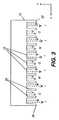
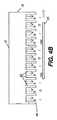
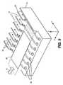
例えば、“GAS DISTRIBUTION SYSTEM FOR CYCLICAL LAYER DEPOSITION”と題される米国特許第6,821,563号明細書(Yudovsky)には、前駆体及びパージガスのための別個のガスポートと、各ガスポート間の真空ポンプポートとを交互に有する、真空下の空間依存性ALD処理システムが記載されている。各ガスポートは、そのガス流を鉛直方向で見て下向きに基板に向かって案内する。別個のガス流は壁又は仕切りによって分離され、各ガス流の両側には排気のための真空ポンプが設けられている。各仕切りの下側部分は、基板に近接して、例えば基板表面から0.5mm以上のところに延びている。このように、これらの仕切りの下側部分は、ガス流が基板表面と反応した後、ガス流が下側部分の周りで真空ポートに向かって流れるのを可能にするのに十分な距離だけ、基板表面から離されている。 For example, US Pat. No. 6,821,563 (Yudovsky) entitled “GAS DISTRIBUTION SYSTEM FOR CYCLICAL LAYER DEPOSITION” includes separate gas ports for precursor and purge gas and between each gas port. A space-dependent ALD processing system under vacuum is described having alternating vacuum pump ports. Each gas port guides the gas flow downward in the vertical direction toward the substrate. Separate gas streams are separated by walls or partitions, and a vacuum pump for evacuation is provided on both sides of each gas stream. The lower part of each partition extends close to the substrate, for example, 0.5 mm or more from the substrate surface. Thus, the lower portion of these partitions is a distance sufficient to allow the gas flow to flow around the lower portion towards the vacuum port after the gas flow has reacted with the substrate surface, Separated from the substrate surface.
回転ターンテーブル又はその他の搬送装置が、1つ又は2つ以上の基板ウエハーを保持するために設けられている。この装置を用いると基板は異なるガス流の下で往復させられ、これによりALD堆積を生じさせる。1つの態様の場合、基板は、チャンバを通して線状通路内で動かされ、この通路内で基板は多数回にわたって前後へパスされる。 A rotating turntable or other transfer device is provided to hold one or more substrate wafers. With this apparatus, the substrate is reciprocated under different gas flows, thereby causing ALD deposition. In one embodiment, the substrate is moved in a linear passage through the chamber, in which the substrate is passed back and forth multiple times.
連続ガス流を使用した別のアプローチが、“METHOD FOR PERFORMING GROWTH OF COMPOUND THIN FILMS”(Suntola他)と題された米国特許第4,413,022号明細書に示されている。ガス流アレイには、ソースガス開口、キャリヤガス開口、及び真空排気開口が交互に設けられている。アレイ上の支持体の往復運動が、パルス化された動作を必要とすることなしに、ここでもALD堆積を生じさせる。具体的には図13及び図14の態様の場合、基板表面と反応性蒸気との順次の相互作用が、ソース開口の固定アレイ上の基板の往復運動によって行われる。排気開口間にキャリヤガス開口を有することにより、拡散バリアが形成されている。このような態様を伴う動作は大気圧においてさえも可能であるとSuntola他は述べているが、プロセスの詳細又は例はほとんど又は全く提供されていない。 Another approach using a continuous gas flow is shown in US Pat. No. 4,413,022, entitled “METHOD FOR PERFORMING GROWTH OF COMPOUND THIN FILMS” (Suntola et al.). The gas flow array has alternating source gas openings, carrier gas openings, and evacuation openings. Again, the reciprocating motion of the support on the array results in ALD deposition without the need for pulsed motion. Specifically, in the case of the embodiment of FIGS. 13 and 14, the sequential interaction between the substrate surface and the reactive vapor is effected by the reciprocation of the substrate on a fixed array of source openings. By having a carrier gas opening between the exhaust openings, a diffusion barrier is formed. Although Suntola et al. State that operation with such aspects is possible even at atmospheric pressure, little or no process details or examples are provided.
‘563 Yudovsky及び‘022 Suntola他の開示物に記載されたもののような方法は、パルス化ガスのアプローチに固有の難しさのいくつかを回避することはできるが、これらのシステムは他の欠点を有する。例えば、アレイ内の異なる地点で均一な真空を維持すること、そして同期的なガス流及び真空を相補的な圧力で維持することは極めて難しく、ひいては基板表面に提供されるガスフラックスの均一性に関して妥協することになる。‘563 Yudovskyの開示物のガス流供給ユニットも、‘022 Suntola他の開示物のガス流アレイも、基板に0.5mmよりも近接して使用することはできない。 While methods such as those described in the '563 Yudovsky and' 022 Suntola et al. Disclosures can avoid some of the difficulties inherent in the pulsed gas approach, these systems have other drawbacks. Have. For example, maintaining a uniform vacuum at different points in the array, and maintaining a synchronized gas flow and vacuum at complementary pressures is extremely difficult, and thus with respect to the uniformity of the gas flux provided to the substrate surface You will compromise. Neither the gas flow supply unit of the '563 Yudovsky disclosure nor the gas flow array of the' 022 Suntola et al. Disclosure can be used closer than 0.5 mm to the substrate.
米国特許出願公開第2005/084610号明細書(Selitser)には、大気圧原子層化学蒸着法が開示されている。動作圧力を大気圧に変化させることにより、反応速度が著しく高くなり、このことは、反応物質の濃度を桁違いに増大させ、その結果として表面反応速度を高めることを、Selitser他は述べている。Selitser他の態様は、方法のそれぞれの段毎に別個のチャンバを伴うが、図10には、チャンバの壁が取り除かれている態様が示されている。一連の分離されたインジェクタが、回転する円形基板ホルダ軌道の周りに間隔を置いて設けられている。各インジェクタは、独立して操作される反応物質マニホルド、パージ・マニホルド、及び排気マニホルドが組み込まれており、そしてそれぞれの基板毎に、この基板がプロセス中にインジェクタの下を通るのに伴って、1つの完結した単分子層堆積・反応物質パージサイクルとして制御し作用する。ガス・インジェクタ又はマニホルドの詳細はほとんど又は全くSelitser他によって記載されてはいないが、隣接するインジェクタからの交差汚染がパージガスによって予防され、排気マニホルドが各インジェクタ内に組み込まれるように、インジェクタの間隔が選択されていると、彼らは述べている。 US 2005/084610 (Selitser) discloses an atmospheric pressure atomic layer chemical vapor deposition process. Changing the operating pressure to atmospheric pressure significantly increases the reaction rate, which increases the concentration of reactants by an order of magnitude and consequently increases the surface reaction rate, Selitser et al. . The Selitser et al. Embodiment involves a separate chamber for each stage of the process, but FIG. 10 shows an embodiment in which the chamber walls have been removed. A series of separate injectors are spaced around a rotating circular substrate holder track. Each injector incorporates an independently operated reactant manifold, purge manifold, and exhaust manifold, and for each substrate, as the substrate passes under the injector during the process, Control and act as one complete monolayer deposition and reactant purge cycle. Little or no details of the gas injectors or manifolds are described by Selitser et al., But the injector spacing is such that cross-contamination from adjacent injectors is prevented by the purge gas and exhaust manifolds are incorporated into each injector. They are selected, they say.
空間依存性ALD法が、2006年3月29日付けで出願された“PROCESS FOR ATOMIC LAYER DEPOSITION”と題される同一譲受人の米国特許出願第11/392,007号明細書(Levy他);2006年3月29日付けで出願された“APPARATUS FOR ATOMIC LAYER DEPOSITION”と題される米国特許出願第11/392,006号明細書(Levy他);2007年1月08日付けで出願された“DEPOSITION SYSTEM AND METHOD USING A DELIVERY HEAD SEPARATED FROM A SUBSTRATE BY GAS PRESSURE”と題される米国特許出願第11/620,744号明細書(Levy);及び2007年1月08日付けで出願された“DELIVERY DEVICE COMPRISING GAS DIFFUSER FOR THIN FILM DEPOSITION”と題される米国特許出願第11/620,740号明細書(Nelson他)に、より詳細に記載された他の装置又はシステムで達成することができる。これらのシステムは、連続的に流れる互いに反応性のガスの望ましくない混和という空間的ALDシステムの困難な局面の1つを克服しようとしている。具体的には、米国特許出願第11/392,007号明細書は、混和を防止するためにシンクの横流パターンを採用しているのに対して、米国特許出願第11/620,744号明細書及び米国特許出願第11/620,740号明細書は、改善されたガス分離を達成するためにプロセスの反応ガスの圧力によって部分的に浮揚された被覆用ヘッドを採用している。 The same assignee's US patent application Ser. No. 11 / 392,007 (Levy et al.) Entitled “PROCESS FOR ATOMIC LAYER DEPOSITION” filed March 29, 2006, for which the spatially dependent ALD method was filed. US Patent Application No. 11 / 392,006 (Levy et al.) Entitled “APPARATUS FOR ATOMIC LAYER DEPOSITION” filed March 29, 2006; filed January 08, 2007 US Patent Application No. 11 / 620,744 (Levy) entitled “DEPOSITION SYSTEM AND METHOD USING A DELIVERY HEAD SEPARATED FROM A SUBSTRATE BY GAS PRESSURE”; and filed on Jan. 08, 2007 Other devices or systems described in greater detail in US patent application Ser. No. 11 / 620,740 (Nelson et al.) Entitled “DELIVERY DEVICE COMPRISING GAS DIFFUSER FOR THIN FILM DEPOSITION” can be achieved. These systems seek to overcome one of the difficult aspects of spatial ALD systems, undesirable mixing of mutually reactive gases with continuous flow. Specifically, US patent application Ser. No. 11 / 392,007 employs a sink cross-flow pattern to prevent mixing, while US patent application Ser. No. 11 / 620,744. And US patent application Ser. No. 11 / 620,740 employ a coating head partially levitated by the pressure of the reaction gas of the process to achieve improved gas separation.
これらの空間依存性ALDシステムの有用性及び使用しやすさにもかかわらず、これらのシステムは互いに反応性のガスの分離という点では、依然として時間依存性ALDシステムよりも能力が低い。従って、これらを工業的に有用にするために、ガス混和に関連する不可避の問題に対してより堅牢な化学物質を考えなければならない。 Despite the usefulness and ease of use of these space-dependent ALD systems, these systems are still less capable than time-dependent ALD systems in terms of separating reactive gases from each other. Therefore, to make them industrially useful, chemicals that are more robust against the inevitable problems associated with gas mixing must be considered.
半導体の性質を化学的に改変するための一般的なアプローチは、半導体の電気的な特性を変化させる他の原子又は分子を半導体のマトリックス内に含むことである。これらの追加の原子は典型的には、システムに可動電荷を受容又は供与することによって働く。酸化亜鉛のような半導体の場合、電子を捕捉し、ひいては半導体の正孔濃度を高め、そしてこの半導体がp型半導体を目指すようにするために、アクセプタ・ドーパントを使用することができる。或いは、電子を放出し、ひいては半導体の電子濃度を高め、そしてこの半導体がn型半導体を目指すようにするために、ドナー・ドーパントを使用することもできる。 A common approach to chemically modify semiconductor properties is to include other atoms or molecules in the semiconductor matrix that alter the electrical properties of the semiconductor. These additional atoms typically work by accepting or donating mobile charges to the system. In the case of semiconductors such as zinc oxide, acceptor dopants can be used to trap electrons and thus increase the hole concentration of the semiconductor and make it aim at a p-type semiconductor. Alternatively, donor dopants can be used to emit electrons and thus increase the electron concentration of the semiconductor and make the semiconductor aim an n-type semiconductor.
酸化亜鉛中のアクセプタ・ドーパントとして使用することができる多数の原子が存在する。これらの原子の中には、窒素、銅、リン、及びヒ素がある。既存の従来技術では、p型酸化亜鉛層を生成しようという試みで、酸化亜鉛中のアクセプタ・ドーパントが使用されている。好適なp型材料は事実、正孔電荷キャリヤ運動に起因して材料を或る程度導電性にするのに十分な正孔濃度を有するように推進されることになる。 There are a number of atoms that can be used as acceptor dopants in zinc oxide. Among these atoms are nitrogen, copper, phosphorus, and arsenic. Existing prior art uses acceptor dopants in zinc oxide in an attempt to produce a p-type zinc oxide layer. A suitable p-type material will in fact be driven to have a hole concentration sufficient to make the material somewhat conductive due to hole charge carrier motion.
例えば、Sugihara他の米国特許出願公開第2006/0244107号明細書には、アクセプタ・ドープ型ZnO系層を調製する方法が開示されている。これらの方法において、膜は、基板温度300℃のパルス化レーザー堆積を利用し、そしてNドーパントとして酸化窒素を使用することにより調製される。興味深いことに、膜は効果を発揮するために、隣接するバリア層を必要とする。 For example, Sugihara et al., US Patent Application Publication No. 2006/0244107, discloses a method for preparing an acceptor-doped ZnO-based layer. In these methods, films are prepared by utilizing pulsed laser deposition at a substrate temperature of 300 ° C. and using nitric oxide as the N dopant. Interestingly, the membrane requires an adjacent barrier layer to be effective.
C. Lee他(J. Vac. Sci. Technol. A 24(4) 2006)は、窒素ドーピングを生成するためのアンモニア・ガスを使用して、ALDタイプの方法によって成長させられたNドープ型ZnO系半導体膜について論じている。これらの膜は、これらをp型ZnOに変換するために1000℃のアニーリングを必要とする。これらは、時間依存性ALD法を用いる。アクセプタ・ドーピングは、p型材料を生成するために用いられる。 C. Lee et al. (J. Vac. Sci. Technol. A 24 (4) 2006), N-doped ZnO grown by an ALD-type method using ammonia gas to generate nitrogen doping. Discusses semiconductor-based semiconductor films. These films require 1000 ° C. annealing to convert them to p-type ZnO. These use a time-dependent ALD method. Acceptor doping is used to produce p-type material.
従って、酸化亜鉛系半導体膜を形成するために、空間依存性ALDシステムを提供することが依然として必要である。 Therefore, it is still necessary to provide a space dependent ALD system in order to form a zinc oxide based semiconductor film.
本発明は、基板上に薄膜材料を堆積することにより、トランジスタに使用するためのn型酸化亜鉛系薄膜半導体を製造する方法であって、細長い実質的に平行なチャネルに沿って一連のガス流を同時に当てることを含み、そして、該一連のガス流が、順番に、少なくとも、第1反応ガス材料と、不活性パージガスと、第2反応ガス材料とを、任意選択的に複数回繰り返された状態で含み、該第1反応ガス材料が、該n型酸化亜鉛系薄膜半導体を形成するために、該第2反応ガス材料で処理された基板表面と反応することができ、該第1反応ガス材料は、亜鉛基及び有機基の両方を含む揮発性有機亜鉛前駆体化合物であり;
揮発性アクセプタ・ドーパント前駆体が、該第1反応ガス材料、第2反応ガス材料、不活性パージガス、又は補足ガス材料の追加のガス流中に導入され;該方法が、実質的に大気圧で又は大気圧を上回る圧力で行われ、そして堆積中の該基板の温度が250℃未満である、n型酸化亜鉛系薄膜半導体を製造する方法に関する。これにより、揮発性アクセプタ・ドーパント前駆体が反応し、酸化亜鉛系薄膜半導体中にアクセプタ・ドーパントとして組み込まれる。The present invention is a method of fabricating an n-type zinc oxide based thin film semiconductor for use in a transistor by depositing a thin film material on a substrate, comprising a series of gas flows along elongated substantially parallel channels. And the series of gas streams is optionally repeated a plurality of times in sequence, at least with the first reactive gas material, the inert purge gas, and the second reactive gas material. The first reactive gas material is capable of reacting with the substrate surface treated with the second reactive gas material to form the n-type zinc oxide thin film semiconductor. The material is a volatile organozinc precursor compound containing both zinc and organic groups;
A volatile acceptor dopant precursor is introduced into an additional gas stream of the first reactive gas material, the second reactive gas material, an inert purge gas, or a supplemental gas material; the method is substantially at atmospheric pressure Alternatively, the present invention relates to a method of manufacturing an n-type zinc oxide-based thin film semiconductor, which is performed at a pressure exceeding atmospheric pressure, and the temperature of the substrate during deposition is less than 250 ° C. As a result, the volatile acceptor / dopant precursor reacts and is incorporated into the zinc oxide thin film semiconductor as an acceptor / dopant.
プロセス中、ガス材料のための基板もしくは堆積装置、又はその両方は、近接する関係を維持しながら、堆積装置の出力面と基板との間の相対運動を提供することができる。 During the process, the substrate for the gas material and / or the deposition apparatus can provide relative movement between the output surface of the deposition apparatus and the substrate while maintaining a close relationship.
好ましい態様の場合、この方法は、薄膜堆積を施される基板の連続的な運動で操作することができ、この方法は、好ましくは、実質的に大気圧の周囲に対して密閉されていない環境内で、堆積装置の傍らを通り過ぎるウェブ上で又はウェブとして支持体を搬送することができる。 In a preferred embodiment, the method can be operated with a continuous motion of the substrate being subjected to thin film deposition, and the method is preferably in an environment that is not substantially sealed to ambient atmospheric pressure. Within, the support can be transported on or as a web passing by the deposition apparatus.
空間的ALD法によって製造された材料の場合、材料の欠陥が2つの有害な影響を及ぼす。先ず第1に、このような材料は、天然電荷キャリヤの余りにも高い濃度を有し、高いオフ電流につながる傾向がある。第2に、このような材料は、バルク電荷作用を招き、不良の閾値下勾配につながるおそれのある欠陥部位を含有する。本発明は、空間依存性ALDシステムにおいて製造された酸化亜鉛系半導体材料が実地で効果的に働くだけでなく、良好な性能を発揮するのを可能にするドーピング法を提供する。 In the case of materials produced by the spatial ALD method, material defects have two detrimental effects. First of all, such materials have too high a concentration of natural charge carriers and tend to lead to high off-currents. Second, such materials contain defect sites that can lead to bulk charge effects and can lead to poor subthreshold gradients. The present invention provides a doping method that allows a zinc oxide based semiconductor material manufactured in a space dependent ALD system to not only work effectively in the field, but also to exhibit good performance.
本発明の利点は、本発明が、数多くの異なるタイプの基板及び堆積環境に適した、基板上への酸化亜鉛系n型半導体の有利な原子層堆積方法を提供することである。 An advantage of the present invention is that it provides an advantageous atomic layer deposition method of zinc oxide-based n-type semiconductors on a substrate that is suitable for many different types of substrates and deposition environments.
本発明のさらに別の利点は、大面積基板上への堆積を含む、ウェブ又はその他の可動基板上の堆積に対して適合可能であることである。 Yet another advantage of the present invention is that it is adaptable for deposition on webs or other movable substrates, including deposition on large area substrates.
本発明のさらに別の利点は、好ましい態様において大気圧条件下での操作を可能にすることである。 Yet another advantage of the present invention is that it allows operation under atmospheric conditions in a preferred embodiment.
本発明のさらに別の利点は、大気圧における低温プロセスにおいて採用することができ、このプロセスを周囲大気に対して開いた、密閉されていない環境内で実施できることである。 Yet another advantage of the present invention is that it can be employed in a low temperature process at atmospheric pressure, and the process can be performed in an unsealed environment open to the ambient atmosphere.
本発明はまた、本発明によって形成された、好ましくは可撓性基板上の酸化亜鉛系半導体を含むトランジスタに関する。 The invention also relates to a transistor comprising a zinc oxide based semiconductor, preferably on a flexible substrate, formed according to the invention.
本発明の方法により製造された半導体膜は、0.1cm2/Vsを上回る優れた電界効果電子移動度、及び104を上回るオンオフ比を膜形態で呈することができ、この性能特性は、アクティブ・マトリックス・ディスプレイ・バックプレーンを含む種々の当該技術において使用するのに十分である。The semiconductor film manufactured by the method of the present invention can exhibit excellent field effect electron mobility exceeding 0.1 cm2 / Vs and an on / off ratio exceeding 104 in the form of a film, and this performance characteristic is It is sufficient for use in a variety of such technologies, including matrix display backplanes.
TFT構造は、酸化亜鉛系半導体に加えて、酸化亜鉛系半導体内に電流を注入するために、ソース及びドレインと一般に呼ばれる導電性電極を含む。本発明によって形成されたnチャネル半導体膜は、nチャネル半導体膜に接続された、互いに離隔された第1コンタクト手段と第2コンタクト手段とをそれぞれ含む薄膜トランジスタに使用することができる。絶縁体によって前記半導体膜から離隔するように第3コンタクト手段を設け、そして第3コンタクト手段に印加される電圧によって、前記膜を通る第1コンタクト手段と第2コンタクト手段との間の電流を制御するように第3コンタクト手段を適合させることができる。第1、第2、及び第3コンタクト手段は、電界効果トランジスタのドレイン、ソース、及びゲート電極に相当することができる。 In addition to the zinc oxide based semiconductor, the TFT structure includes conductive electrodes commonly referred to as a source and a drain to inject current into the zinc oxide based semiconductor. The n-channel semiconductor film formed according to the present invention can be used for a thin film transistor including first contact means and second contact means which are connected to the n-channel semiconductor film and are separated from each other. Third contact means is provided so as to be separated from the semiconductor film by an insulator, and current between the first contact means and the second contact means passing through the film is controlled by a voltage applied to the third contact means. The third contact means can be adapted to do so. The first, second, and third contact means may correspond to the drain, source, and gate electrodes of the field effect transistor.
本発明のこれらの及びその他の目的、特徴、及び利点は、本発明の一例としての態様を示し記述した図面と併せて、下記詳細な説明を読めば、当業者には明らかになる。 These and other objects, features and advantages of the present invention will become apparent to those of ordinary skill in the art by reading the following detailed description, taken in conjunction with the drawings which illustrate and describe illustrative aspects of the invention.
本明細書は、本発明の主題を具体的に指摘し明確に主張する特許請求の範囲で締めくくられるが、添付の図面と併せて下記説明から本発明をより良く理解することができる。 While the specification concludes with claims that particularly point out and distinctly claim the subject matter of the invention, the invention may be better understood from the following description in conjunction with the appended drawings.
この方法に従って形成される半導体膜は、0.01cm2/Vs超、好ましくは少なくとも0.1cm2/Vs、より好ましくは1cm2/Vs超の電界効果電子移動度を示す。加えて、この発明の方法に従って形成されるnチャネル半導体膜は、少なくとも104、有利には少なくとも105又は106のオンオフ比を提供することができる。The semiconductor film formed according to this method exhibits a field effect electron mobility of greater than 0.01 cm2 / Vs, preferably at least 0.1 cm2 / Vs, more preferably greater than 1 cm2 / Vs. In addition, the n-channel semiconductor film formed according to the method of the invention can provide an on / off ratio of at least 104 , advantageously at least 105 or 106 .
さらに、可視光によるデバイスへの影響は弱いものであるか又は全くないことが望ましい。これを真に実現するためには、半導体バンドギャップは、可視光に対する曝露がバンド間遷移を引き起こさないように十分に大きく(>3eV)なければならない。 Furthermore, it is desirable that visible light has little or no effect on the device. In order to truly achieve this, the semiconductor band gap must be large enough (> 3 eV) so that exposure to visible light does not cause interband transitions.
酸化亜鉛系材料が、高い移動度、低いキャリヤ濃度、及び高いバンドギャップをもたらすことができる。さらに、ウェブに基づく大気中での真の大量生産スキームでは、プロセスに使用される化学物質が低廉且つ低毒性であることが非常に望ましい。このような条件は、ZnO系材料及びその前駆体の大部分を使用することにより満たされる。 Zinc oxide-based materials can provide high mobility, low carrier concentration, and high band gap. Furthermore, in true mass production schemes in the air based on the web, it is highly desirable that the chemicals used in the process are cheap and low toxic. Such a condition is satisfied by using the majority of ZnO-based materials and their precursors.
酸化亜鉛系半導体材料は、半導体酸化物を形成することができる少量の他の金属、例えばインジウム、錫、又はカドミウム、及びこれらの組み合わせを含有することができる。例えば、Chiang, H. Q.他“High mobility transparent thin-film transistors with amorphous zinc tin oxide channel layer” Applied Physics Letters 86, 013503 (2005)は、酸化亜鉛錫材料を開示している。 Zinc oxide-based semiconductor materials can contain small amounts of other metals that can form semiconductor oxides, such as indium, tin, or cadmium, and combinations thereof. For example, Chiang, H. Q. et al. “High mobility transparent thin-film transistors with amorphous zinc tin oxide channel layer” Applied Physics Letters 86, 013503 (2005) discloses zinc oxide tin materials.
従って、「酸化亜鉛系」という用語は、大部分、好ましくは少なくとも80パーセントが酸化亜鉛から成る組成物を意味するが、しかし少量の他の金属酸化物を含む添加剤又は混合物を許す。このような半導体組成物は当業者に知られている。 Thus, the term “zinc oxide-based” means a composition that consists mostly of zinc oxide, preferably at least 80 percent, but allows additives or mixtures containing small amounts of other metal oxides. Such semiconductor compositions are known to those skilled in the art.
名目上ドープされていない酸化亜鉛は、浅い(shallow)ドナーの存在によりn型導電率を示す。化学量論からの偏差に起因する格子欠陥は、浅いドナー状態を形成する役割を演じると考えられるが、意図せずに組み込まれた水素も、浅いドナー状態源と考えられる。D. C. Look, J. R. Sizelove及びJ. W. Hemsky, Phys. Rev. Lett. 82, 2552-2555(1999); C. G. Van de Walle, Phys. Rev. Lett. 85 1012 (2000)を参照されたい。これらの浅いドナーは通常、酸化亜鉛の伝導バンドエッジより100meV未満下回る占有エネルギーレベルを導入するようになっている。これらの浅いドナーの状態を占有する電子は、熱励起を介して伝導バンド内に促進することができ、固有導電率をもたらすことができる。 Nominally undoped zinc oxide exhibits n-type conductivity due to the presence of a shallow donor. Lattice defects due to deviations from stoichiometry are thought to play a role in forming shallow donor states, but unintentionally incorporated hydrogen is also considered a source of shallow donor states. See D. C. Look, J. R. Sizelove and J. W. Hemsky, Phys. Rev. Lett. 82, 2552-2555 (1999); C. G. Van de Walle, Phys. Rev. Lett. 85 1012 (2000). These shallow donors are usually adapted to introduce an occupied energy level that is less than 100 meV below the conduction band edge of zinc oxide. Electrons occupying these shallow donor states can be promoted into the conduction band via thermal excitation, resulting in intrinsic conductivity.
オフ電流を改善するために、酸化亜鉛系半導体は、少数の天然電荷キャリヤを有し、高い抵抗をもたらすべきである。本発明によれば、ZnOの抵抗率は、揮発性有機化合物から形成されたアクセプタ・ドーパント、例えばN、P、As、Li、Na、K、Cu、Ag又はこれらの混合物のようなアクセプタ・ドーパントを含む揮発性化合物で置換ドープすることにより高められる。好ましくは、アクセプタ・ドーパントは、V族元素、より好ましくは窒素を含み、例えばアクセプタ・ドーパントが、NO、N2O、NO2、又はアンモニアの形態の窒素を含む。In order to improve off current, zinc oxide based semiconductors should have a small number of natural charge carriers and provide high resistance. According to the present invention, the resistivity of ZnO is an acceptor dopant formed from a volatile organic compound, such as an acceptor dopant such as N, P, As, Li, Na, K, Cu, Ag or mixtures thereof. It is enhanced by substitution doping with a volatile compound containing. Preferably, the acceptor dopant comprises a group V element, more preferably nitrogen, for example, the acceptor dopant comprises nitrogen in the form of NO, N2 O, NO2 , or ammonia.
典型的には、V族元素が酸素と置き換わるのか又はI族又はIB族元素が亜鉛と置き換わるのかとはかかわりなく、アクセプタ・ドーパントは、これが置き換わる原子よりも少ない価電子を有している。 Typically, regardless of whether the Group V element replaces oxygen or the Group I or IB element replaces zinc, the acceptor dopant has fewer valence electrons than the atom it replaces.
本発明の好ましい態様の場合、アクセプタ・ドーパントなしの半導体のオンオフ比は、1.0×10⁶未満である。また、アクセプタ・ドーパントの存在は、抵抗率を少なくとも102増大させ、アクセプタ・ドーパントなしの半導体の抵抗率は、500オーム・cm未満である。特に好ましい態様の場合、アクセプタ・ドーパントの存在は、移動度を少なくとも25%、より好ましくは少なくとも50%増大させる。In a preferred embodiment of the invention, the on / off ratio of the semiconductor without acceptor dopant is less than 1.0 × 10⁶ . Also, the presence of the acceptor dopant increases the resistivity by at least 102 , and the resistivity of the semiconductor without the acceptor dopant is less than 500 ohm · cm. In a particularly preferred embodiment, the presence of acceptor dopant increases the mobility by at least 25%, more preferably by at least 50%.
揮発性化合物は、ガスの形態で反応チャンバに供給されることができるように、室温において或る程度は蒸気相で存在し得る化合物として定義される。このようなガスが、堆積法に有用な影響を与えるのに十分な揮発性材料を含有するために、揮発性化合物は、0.1mmHgを上回る、好ましくは1mmHgを上回る室温における蒸気圧を有するのが好ましい。そのようなドーパントは好ましくは、0.001%〜5%、より好ましくは0.01%〜1%の量で最終半導体内に存在する。 Volatile compounds are defined as compounds that can exist to some extent in the vapor phase at room temperature so that they can be supplied to the reaction chamber in the form of a gas. In order for such a gas to contain enough volatile material to have a useful effect on the deposition process, the volatile compound has a vapor pressure at room temperature above 0.1 mmHg, preferably above 1 mmHg. Is preferred. Such dopant is preferably present in the final semiconductor in an amount of 0.001% to 5%, more preferably 0.01% to 1%.
本発明の範囲に含まれるアクセプタ・ドーパントは、浅いドナーのエネルギーレベルを下回り、且つ電子を受容することができるZnO系材料のバンドギャップ内にエネルギーレベルを導入する不純物である。このようなアクセプタ・ドーパントは、これが置き換わる原子よりも少ない価電子を有する不純物原子であってよい。ZnO系材料の例は、酸素と置き換わるV族元素、例えば窒素、リン又はヒ素、及び亜鉛と置き換わるI族及びIB族元素、例えばリチウム、ナトリウム、カリウム、銅又は銀である。U. Ozgur, Ya. I. Alivov, C. Liu, A. Teke, M.A. Reshchikov, S. Doan, V. Avrutin, S.-J. Cho、及びH. Morkoc, J. Appl. Phys. 98 041301 (2001)を参照されたい。 Acceptor dopants within the scope of the present invention are impurities that introduce energy levels within the band gap of ZnO-based materials that are below the energy level of shallow donors and can accept electrons. Such acceptor dopant may be an impurity atom having fewer valence electrons than the atom it replaces. Examples of ZnO-based materials are Group V elements that replace oxygen, such as nitrogen, phosphorus or arsenic, and Group I and IB elements that replace zinc, such as lithium, sodium, potassium, copper, or silver. U. Ozgur, Ya. I. Alivov, C. Liu, A. Teke, MA Reshchikov, S. Doan, V. Avrutin, S.-J. Cho and H. Morkoc, J. Appl. Phys. 98 041301 ( 2001).
加えて、当業者に知られている種々の任意選択的なコンベンショナルな少量のドーパント、好ましくは10重量パーセント未満のドーパントを、堆積中又は堆積後に酸化亜鉛系半導体内に含むこともできる。チャネル層の厚さは種々様々であってよく、具体例によれば、これは5nm〜500nm、10nm〜50nmであってよい。 In addition, various optional conventional small amounts of dopants known to those skilled in the art, preferably less than 10 weight percent, may be included in the zinc oxide based semiconductor during or after deposition. The thickness of the channel layer may vary, and according to a specific example, this may be 5 nm to 500 nm, 10 nm to 50 nm.
チャネルの長さ及び幅は、画素サイズ、及び構築中のシステムの設計ルールによって決定される。典型的には、チャネル幅は10〜1000μmであってよい。チャネル長は種々様々であってよく、具体例によれば、これは1〜100μmであってよい。 The length and width of the channel are determined by the pixel size and the design rules of the system under construction. Typically, the channel width may be 10 to 1000 μm. The channel length may vary, and according to a specific example, this may be 1-100 μm.
本発明の薄膜トランジスタ又は電子デバイスを製造するプロセス全体、又は少なくとも薄膜半導体の製造は、最大支持温度300℃未満、より好ましくは250℃未満、又はおよそ室温の温度(25℃〜70℃)でも行うことができる。ここに含まれる本発明に関する知識を持っているならば、温度選択は一般に、当業者に知られている支持体及び処理パラメータに応じて行う。これらの温度は伝統的な集積回路及び半導体の処理温度を十分に下回る。これにより、種々の比較的低廉な支持体、例えば可撓性高分子支持体のいずれかの使用が可能になる。こうして、本発明は、性能が著しく改善された薄膜トランジスタを含有する比較的低廉な回路の製造を可能にする。 The entire process of manufacturing the thin film transistor or electronic device of the present invention, or at least the manufacture of the thin film semiconductor, should be performed at a maximum support temperature of less than 300 ° C, more preferably less than 250 ° C, or even at a temperature of about room temperature (25 ° C to 70 ° C) Can do. Given the knowledge of the invention contained herein, the temperature selection is generally made according to the support and processing parameters known to those skilled in the art. These temperatures are well below traditional integrated circuit and semiconductor processing temperatures. This allows the use of any of a variety of relatively inexpensive supports, such as flexible polymer supports. Thus, the present invention enables the manufacture of relatively inexpensive circuits that contain thin film transistors with significantly improved performance.
以下の説明に関して「ガス」又は「ガス材料」という用語は、広い意味で、所定の範囲の蒸発した又はガス状の元素、化合物、もしくは材料のいずれかを含むように使用される。本明細書中に使用されるその他の用語、例えば「反応物質」、「前駆体」、「真空」及び「不活性ガス」は、材料堆積技術における当業者によってよく理解される従来通りの意味を有する。提供される図面は、原寸に比例して描かれてはいないが、本発明のいくつかの態様の機能全体及び構造的配列を示すように意図されている。 In the following description, the terms “gas” or “gas material” are used in a broad sense to include any range of evaporated or gaseous elements, compounds, or materials. Other terms used herein, such as “reactant”, “precursor”, “vacuum” and “inert gas” have their conventional meanings well understood by those skilled in the material deposition arts. Have. The drawings provided are not drawn to scale, but are intended to illustrate the overall functionality and structural arrangement of some aspects of the present invention.
本発明の装置は、酸化亜鉛系n型半導体膜を製造することに対する従来のアプローチからの有意義な脱却を提供し、大面積の、ウェブをベースとする基板上への堆積に適合することができ、また改善されたスループット速度で高度に均一な薄膜堆積を達成することができる、基板表面にガス材料を供給するためのシステムを採用する。本発明の方法は、(パルス化ALD又は時間依存性ALDとは反対に)連続した空間依存性ALDガス材料分配を採用する。本発明の方法は、大気圧又は近大気圧並びに真空下での動作を可能にし、また、密閉されていない又はオープンエア環境内で動作することができる。 The apparatus of the present invention provides a significant departure from conventional approaches to producing zinc oxide based n-type semiconductor films and can be adapted for deposition on large area, web based substrates. It also employs a system for supplying a gas material to the substrate surface that can achieve highly uniform thin film deposition at an improved throughput rate. The method of the present invention employs a continuous space-dependent ALD gas material distribution (as opposed to pulsed ALD or time-dependent ALD). The method of the present invention allows operation under atmospheric or near atmospheric pressure as well as under vacuum and can operate in an unsealed or open air environment.
図1は、本発明の態様による酸化亜鉛系n型半導体膜を製造する方法の1つの態様の一般化された工程ダイヤグラムである。ここでは、第1分子前駆体と第2分子前駆体とから成る2種の反応性ガスが使用される。ガスはガス源から供給され、そして例えば堆積装置を介して基板に供給することができる。ガス材料を堆積装置に提供する計量・弁装置を使用することができる。 FIG. 1 is a generalized process diagram of one embodiment of a method of manufacturing a zinc oxide based n-type semiconductor film according to an embodiment of the present invention. Here, two types of reactive gases composed of a first molecular precursor and a second molecular precursor are used. The gas is supplied from a gas source and can be supplied to the substrate, for example, via a deposition apparatus. A metering and valve device can be used that provides the gas material to the deposition device.
工程1に示されているように、システムのためのガス材料の連続供給が、基板上の材料薄膜を堆積するために行われる。シーケンス15における工程は順次適用される。工程2において、基板の所与の領域(チャネル領域と呼ぶ)に関して、第1分子前駆体又は反応ガス材料が、基板のチャネル領域上で第1チャネル内を流れるように導かれ、この領域と反応する。工程3において、基板とシステム内のマルチ・チャネル流との相対運動が発生し、このことが工程4の準備を整える。工程4では、不活性ガスを有する第2チャネル(パージ)流が、所与のチャネル領域の上方で発生する。次いで工程5において、基板とマルチ・チャネル流との相対運動が工程6の準備を整える。工程6では、所与のチャネル領域に原子層堆積が施され、ここでは第2分子前駆体が今や(この特定の態様では基板の表面に対して横方向且つ実質的に平行に)基板の所与のチャネル領域上に位置し、基板上の前の層と反応することにより、所望の材料の(理論上)単分子層を生成する。第1分子前駆体は、ガス形態の亜鉛含有化合物であり、堆積される材料は、亜鉛含有化合物、例えば有機亜鉛化合物、例えばジエチル亜鉛である。このような態様の場合、第2分子前駆体は、例えば非金属酸化化合物であってよい。揮発性アクセプタ・ドーピング化合物は、これが成長中の膜内の部位に対して反応するのを可能にする任意の方法で、システムに供給することができる。このように、揮発性アクセプタ・ドーピング化合物は、第1又は第2分子前駆体と、又はパージガスと一緒に供給することができる。好ましくは、揮発性アクセプタは、酸化分子前駆体と一緒に供給される。 As shown in
工程7では、基板とマルチ・チャネル流との相対運動が次いで、工程8の準備を整える。工程8では再び、不活性ガスを使用することにより、この時には、前の工程6から生じた所与のチャネル領域からの過剰の第2分子前駆体を一掃する。工程9において、基板とマルチ・チャネル流との相対運動が再び発生し、このことが、工程2へ戻る反復シーケンスの準備を整える。サイクルは、所望の膜を確立するのに必要な回数だけ反復される。この方法のこの態様の場合、工程は、流れチャネルによって占められる領域に対応する、基板の所与のチャネル領域に対して繰り返される。その間に、種々のチャネルには、工程1の所要のガス材料が供給されることになる。図1のボックス15のシーケンスと同時に、他の隣接チャネル領域が処理され、その結果、工程11全体に示されているように、マルチ・チャネル流が並行して生じる。並行流は、堆積装置の出力面に対して実質的に直交方向又は実質的に平行に生じることができる。 In step 7, the relative motion of the substrate and the multi-channel flow is then ready for step 8. Step 8 again uses an inert gas, thereby sweeping away any excess second molecular precursor from a given channel region resulting from the previous step 6. In step 9, relative motion between the substrate and the multi-channel flow occurs again, ready for an iterative sequence returning to step 2. The cycle is repeated as many times as necessary to establish the desired membrane. For this aspect of the method, the process is repeated for a given channel region of the substrate that corresponds to the region occupied by the flow channel. In the meantime, the various channels will be supplied with the required gas material of
第2分子前駆体の主要な目的は、基板表面を、第1分子前駆体と反応する方向に戻るように状態調節することである。第2分子前駆体はまた、分子ガスから材料を提供することにより、表面の金属と合体し、堆積したばかりの亜鉛含有前駆体と酸化物を形成する。 The main purpose of the second molecular precursor is to condition the substrate surface so that it returns in a direction to react with the first molecular precursor. The second molecular precursor also merges with the surface metal by providing material from the molecular gas to form an oxide with the just-deposited zinc-containing precursor.
特定の態様は、分子前駆体を基板に適用した後で分子前駆体を除去するために真空パージを用いる必要がない。パージ工程はALD法における最も顕著なスループット制限工程であると、大抵の研究者が予測している。 Certain embodiments do not require the use of a vacuum purge to remove the molecular precursor after it has been applied to the substrate. Most researchers predict that the purge process is the most significant throughput limiting process in ALD.
図1における2種の反応ガスとして、例えばAX及びBYを使用すると想定する。反応ガスAX流が供給され、所与の基板領域上に流されると、反応ガスAXの原子は基板上に化学吸着され、その結果Aから成る層と、リガンドXの表面とが生じる(会合化学吸着)(工程2)。次いで、残りの反応ガスAXは不活性ガスでパージされる(工程4)。次いで反応ガスBY流が供給され、及びAX(表面)とBY(ガス)とが化学反応し、その結果、基板上にABから成る分子層が生じる(解離化学吸着)(工程6)。残りのガスBY及び反応副産物はパージされる(工程8)。薄膜の厚さは、プロセス・サイクル(工程2〜9)を多数回繰り返すことにより増大させることができる。 Assuming that, for example, AX and BY are used as the two reaction gases in FIG. When a reactive gas AX stream is supplied and flowed over a given substrate region, the atoms of the reactive gas AX are chemisorbed onto the substrate, resulting in a layer of A and a surface of the ligand X (association chemistry). Adsorption) (Step 2). Next, the remaining reaction gas AX is purged with an inert gas (step 4). Next, a reactive gas BY flow is supplied, and AX (surface) and BY (gas) chemically react with each other, resulting in a molecular layer composed of AB on the substrate (dissociation chemisorption) (step 6). The remaining gas BY and reaction byproducts are purged (step 8). The thickness of the thin film can be increased by repeating the process cycle (steps 2-9) many times.
膜は一度に1つの単分子層上に堆積することができるので、コンフォーマルであり均一な厚さを有する傾向がある。 Because films can be deposited on one monolayer at a time, they tend to be conformal and have a uniform thickness.
本発明の方法を用いて形成することができる酸化物の一例としては、ZnO、酸化インジウム、酸化錫が挙げられる。本発明の方法を用いて形成することができる混合構造酸化物は、例えばInZnO及びInGaZnOを含むことができる。本発明の方法を用いて形成することができるドープ型材料は、例えばZnO:Al、GaInZnO、MgxZn1-xO、及びLiZnOを含むことができる。Examples of oxides that can be formed using the method of the present invention include ZnO, indium oxide, and tin oxide. Mixed structure oxides that can be formed using the method of the present invention can include, for example, InZnO and InGaZnO. Doped materials that can be formed using the method of the present invention can include, for example, ZnO: Al, GaInZnO, Mgx Zn1-x O, and LiZnO.
当業者には明らかなように、2種、3種又は4種以上の金属の合金を堆積することができ、2種、3種又は4種以上の成分と一緒に化合物を堆積することができ、また等級フィルム及びナノ−ラミネートのようなものを製造することもできる。 As will be apparent to those skilled in the art, alloys of two, three, four or more metals can be deposited, and compounds can be deposited with two, three, four or more components. It is also possible to produce things such as grade films and nano-laminates.
これらのバリエーションは、交互のサイクルで本発明の特定の態様を用いた変更形に過ぎない。 These variations are only variations using certain aspects of the invention in alternating cycles.
種々の揮発性亜鉛含有前駆体、前駆体の組み合わせ、及びALD薄膜法において有用な反応物質に関しては、Handbook of Thin Film Process Technology, Vol. 1, Glocker及びShah編, Institute of Physics (IOP) Publishing, Philadelphia 1995, 第B1.5:1〜B1.5:16頁;Handbook of Thin Film Material, Nalwa編, Vol.1, 第103〜159頁を参照されたい。 For various volatile zinc-containing precursors, precursor combinations, and reactants useful in ALD thin film methods, see Handbook of Thin Film Process Technology, Vol. 1, Glocker and Shah, Institute of Physics (IOP) Publishing, See Philadelphia 1995, B1.5: 1-B1.5: 16; Handbook of Thin Film Material, edited by Nalwa, Vol. 1, pages 103-159.
酸化物基板はALD堆積のための基を提供するが、好適な表面処理によってプラスチック基板を使用することができる。 Although an oxide substrate provides a group for ALD deposition, a plastic substrate can be used with a suitable surface treatment.
ここで図2を参照すると、本発明による基板20上への酸化亜鉛系半導体の原子層堆積のために本発明の方法において使用することができる堆積装置10の1つの態様の断面側方図が示されている。堆積装置10は、第1ガス材料を受容するためのガス流入ポート14と、第2ガス材料を受容するためのガス流入ポート16と、第3ガス材料を受容するためのガス流入ポート18とを有している。これらのガスは、続いて説明する構造的配列を有する出力チャネル12を介して、出力面36で放出される。図2及び後続の図3〜4Bにおける矢印は、ガス材料の拡散輸送を意味するものであって、出力チャネルから受容された流れを意味するものではない。この特定の態様において、流れは、さらに下で説明するように、実質的に図面頁から出るように導かれる。 Referring now to FIG. 2, a cross-sectional side view of one embodiment of a
1つの態様の場合、ALD堆積を生じさせるために基板表面上で順次反応する第1及び第2ガスを受容するように、ガス流入ポート14及び16が適合されており、ガス流入ポート18が、第1及び第2ガスに対して不活性のパージガスを受容する。堆積装置10は、後でより詳細に説明するように基板支持体上に設けられた基板20から距離Dを置いて配置されている。基板20と堆積装置10との間には、基板20の運動によって、又は堆積装置10の運動によって、又は基板20及び堆積装置10の両方の運動によって、往復運動を提供することができる。図2に示された特定の態様の場合、矢印R、及び図2の基板20の左右の仮想線によって示すように、往復式に出力面36を横切るように、基板20が動かされる。なお、往復運動は、堆積装置10を使用する薄膜堆積にいつも必要とされるわけではない。基板20と堆積装置10との間の他のタイプの相対運動、例えば後でより詳細に説明するような、基板20又は堆積装置10の1つ又は2つ以上の方向における運動を提供することもできる。 In one embodiment, the
図3の断面図は、堆積装置10の出力面36の一部の上方に放出されたガス流を示している。この特定の配列において、仕切り22によって分離された各出力チャネル12は、図2に見られるガス流入ポート14,16又は18のうちの1つとガス流体連通している。各出力チャネル12は典型的には、第1反応ガス材料O、又は第2反応ガス材料M、又は第3不活性ガス材料Iを供給する。 The cross-sectional view of FIG. 3 shows the gas flow released above a portion of the
図3は、ガスの比較的基本的又は単純な配列を示している。複数の(材料Oのような)非金属堆積前駆体流、又は少なくとも(材料Mのような)亜鉛含有前駆体を含む複数の金属含有前駆体材料流を、薄膜単一堆積の際に種々のポートに順次供給することも考えられる。或いは、例えば交互の金属層を有する、又は金属酸化物材料中に混和された少量のドーパントを有する複合薄膜材料を形成するときに、反応ガスの混合物、例えば、金属前駆体材料の混合物、又は金属及び非金属前駆体の混合物を単一の出力チャネルに適用することもできる。符号Iを付けられた中間流が、ガスがその中で互いに反応する見込みのあるいかなる反応物質チャネルをも分離する。第1及び第2反応ガス材料O及びMは、ALD堆積を生じさせるために互いに反応するが、しかし反応ガス材料O又はMも不活性ガス材料Iとは反応しない。図3以降に使用された用語は、何らかの典型的なタイプの反応ガスを示唆している。例えば、第1反応ガス材料Oは、酸化ガス材料であってもよく、第2反応ガス材料Mは、金属亜鉛含有化合物となる。不活性ガス材料Iは、窒素、アルゴン、ヘリウム、又はALDシステムにおけるパージガスとして一般に使用されるその他のガスであってよい。不活性ガス材料Iは、第1及び第2反応ガス材料O及びMに対して不活性である。第1及び第2反応ガス材料間の反応は、金属酸化物又はその他の二元化合物、例えば1つの態様において酸化亜鉛ZnOを形成することになる。3種以上の反応ガス材料間の反応は三元化合物、例えばZnAlOを形成することもできる。 FIG. 3 shows a relatively basic or simple arrangement of gases. A plurality of non-metal deposition precursor streams (such as material O) or a plurality of metal-containing precursor material streams including at least a zinc-containing precursor (such as material M) It is also possible to supply the ports sequentially. Alternatively, for example, when forming a composite thin film material having alternating metal layers or having a small amount of dopant admixed in a metal oxide material, a mixture of reactive gases, such as a mixture of metal precursor materials, or metal And a mixture of non-metallic precursors can be applied to a single output channel. An intermediate stream labeled I separates any reactant channels in which the gas is likely to react with each other. The first and second reactive gas materials O and M react with each other to cause ALD deposition, but the reactive gas material O or M does not react with the inert gas material I. The terminology used in FIG. 3 and beyond suggests some typical type of reaction gas. For example, the first reactive gas material O may be an oxidizing gas material, and the second reactive gas material M is a metal zinc-containing compound. Inert gas material I may be nitrogen, argon, helium, or other gases commonly used as purge gases in ALD systems. The inert gas material I is inert to the first and second reaction gas materials O and M. The reaction between the first and second reactant gas materials will form a metal oxide or other binary compound, such as zinc oxide ZnO in one embodiment. Reactions between three or more reactive gas materials can also form ternary compounds, such as ZnAlO.
図4A及び4Bの断面図は、反応ガス材料O及びMを供給するときに基板20が堆積装置10の出力面36に沿って進むのに伴って実施されるALD被覆動作を、単純化された概略形態で示している。図4Aにおいて、基板20の表面は先ず、第1反応ガス材料Oを供給するものとして指定された出力チャネル12から連続的に放出された酸化材料を受容する。基板の表面はここでは、材料Oの部分反応形態を含有している。この部分反応形態は、材料Mと反応させられ易い。次いで、基板20が第2反応ガス材料Mの金属化合物の経路内に入ると、Mとの反応が行われ、金属酸化物、又は2つの反応ガス材料から形成することができる何らかの他の薄膜材料を形成する。 The cross-sectional views of FIGS. 4A and 4B simplified the ALD coating operation that is performed as the
図4A及び4Bが示すように、第1及び第2反応ガス材料O及びMの流れの間の交互の出力チャネル12毎には不活性ガス材料Iが提供されている。
連続する出力チャネル12が隣接しており、すなわち、図示の態様では仕切り22によって形成された共通の境界を共有している。ここでは、出力チャネル12は、基板20の表面に対して垂直に延びる仕切り22によって互いに画定され分離されている。As shown in FIGS. 4A and 4B, an inert gas material I is provided for each
上述のように、この特定の態様の場合、出力チャネル12間に真空チャネルは散在していない。すなわち、仕切りの周りのガス材料を引き出すために、ガス材料供給チャネルのいずれかの側にも真空チャネルは設けられていない。この有利なコンパクトな配列は、革新的なガス流が使用されている理由から可能である。基板に対して実質的に鉛直方向(すなわち垂直方向)のガス流を加え、次いで対向鉛直方向に使用済ガスを引き抜くようになっている以前の一連のガス供給処理とは異なり、堆積装置10は、各反応ガス及び不活性ガス毎に表面に沿ってガス流(1つの態様の場合、好ましくは実質的に層流)を導き、そして続いて説明するように、使用済ガス及び反応副産物を異なる形で処理する。本発明において使用されるガス流は、基板表面平面に沿って、そして基板表面平面に対して概ね平行に導かれる。換言すれば、ガス流は、処理される基板に対して垂直ではなく、基板平面に対して実質的に横方向に導かれる。 As mentioned above, in this particular embodiment, vacuum channels are not interspersed between
図5及び6は、出力面36から(すなわち図2〜4Bに対して下側から)見た、本発明の方法に使用することができる堆積装置10の1つの態様の斜視図を示している。この態様において隣接する出力チャネル12を画定して分離する仕切り22は、部分的に破断して、ガス出力ポート24から流れるガス流をより良く見えるように示している。図5及び6はまた、この開示の図面に使用した、基準x、y、z座標軸の割り当てを示している。出力チャネル12が実質的に平行に形成されていて、x座標軸に相当する長さ方向に延びている。基板20の往復運動、又は基板20に対する相対運動が、この座標の割り当てを用いると、y座標方向で行われる。 FIGS. 5 and 6 show perspective views of one embodiment of the
図6は、この態様の堆積装置10から供給された種々のガス材料に対応するガス流FI、FO及びFMを示す。ガス流FI、FO及びFMはx方向、すなわち細長い出力チャネル12の長さに沿って形成される。FIG. 6 shows gas flows FI , FO and FM corresponding to various gas materials supplied from the
図7A、7B、7C及び7Dの断面図は、図2〜4Bの断面に対して直交方向に示されており、そしてこの図で見て1つの方向のガス流を示している。各出力チャネル12内部では、相応のガス材料が、図7A、7B、7C及び7Dで仮想線で示されたガス出力ポート24から流れる。図7Aの態様の場合、ガス流F1は、図5及び6を参照して説明したように、出力チャネル12の長さに沿って、そして基板20を横切るように、ガス材料を当てる。流れF1はこの配列の堆積装置10のエッジを超えて持続し、周囲環境内に流出するか、又は所望の場合にはガス捕集マニホルド(図示せず)に流れる。図7Bは、出力チャネル12がガス流の再指向又は引き抜きのための排気ポート26をも提供する、ガス流F2のための別の態様を示している。図7Cは、ガス出力ポート24が、出力チャネル12内部の中央に配置され、チャネルに沿って両方向にガス流中のガス材料を当てる、ガス流F3のための別の態様を示している。図7Dは、ガス出力ポート24がやはり中央に配置されていて、複数の排気ポート26が出力チャネル12の最端部近くに好適に配置されている、ガス流F4のための別の態様を示している。一方向流が好ましいが、或る程度の混合が発生することがあり、このような混合は、また特定の用途に関与する流量及びその他の環境に応じて、或る程度有益なことさえある。 The cross-sectional views of FIGS. 7A, 7B, 7C and 7D are shown orthogonal to the cross-sections of FIGS. 2-4B and show gas flow in one direction as viewed in this view. Within each
特定の堆積装置10は、ガス流形態又はこれらの組み合わせ、図7AのF1流、図7BのF2流、図7CのF3流、図7DのF4流、又は、好ましくは制御された混合とともに層状又は平滑に、出力チャネル12に沿って基板20を横切って流れるようにガス材料が導かれる何らかの他の変更形のうちのいずれか1つを使用して構成された出力チャネル12を使用してよい。1つの態様の場合、反応ガス材料を供給する各出力チャンネル12毎に1つ又は2つ以上の排気ポート26が設けられている。例えば、図6を参照すると、符号O及びMで示された第1及び第2反応ガス材料のための出力チャネル12が、流れF2(図7B)のパターンに従って、反応物質を通気するか又は引き抜くために排気ポート26を有するように構成されている。このことは、何らかの材料再循環を許し、またマニホルドの端部の近くの不所望の混合及び反応を防止する。符号Iで示された不活性ガス材料のための出力チャネル12は、排気ポート26を使用せず、ひいては流れF1(図7A)のパターンに従う。層流がいくつかの態様において好ましいが、或る程度の混合が発生することがあり、このような混合は、また特定の用途に関与する流量及びその他の環境に応じて、或る程度有益なことさえある。
排気ポート26は従来の意味で真空ポートである必要はなく、単に、その対応出力チャネル12内のガス流を引き抜き、ひいてはチャネル内部の均一なガス流パターンを促進するために設けられているに過ぎない。ガス出力ポート24におけるガス圧力の対向圧力よりもわずかに低い負の吸引力が、秩序正しい流れを促進するのを助けることができる。負の吸引は、例えば0.9〜1.0気圧の圧力で動作することができるのに対して、典型的な真空は例えば0.1気圧未満である。流れパターンを排気ポート26内に再指向するために、図7B及び7Dに点線で輪郭を示した任意選択的にバッフル58が設けられていてよい。 The
仕切り22の周りのガス流を真空排気する必要がないので、出力面36は、基板表面から1ミル(ほぼ0.025mm)以内に、極めて近接して配置することができる。比較によると、前に引用した米国特許第6,821,563号明細書(Yudovsky)に記載されているような以前のアプローチは、チャネル側壁のエッジの周りのガス流を必要とし、ひいては基板表面に対して0.5mm以上の距離に限定された。本発明では、基板表面に堆積装置10がより近接して配置されることが好ましい。好ましい態様の場合、基板表面からの距離Dは、堆積装置の出力面、又は流れチャネルを形成するガイド壁の底部から0.4mm以下、好ましくは0.3mm以内、より好ましくは0.25mm以内であってよい。 Since there is no need to evacuate the gas flow around the
図8A及び8Bの断面図は、本発明において用いられる作業と呼応して、なぜ距離Dが比較的小さいことが望ましいかを示している。これらの図面において、堆積装置10は、矢印が示すように左から右へ基板20上を運動している。反応ガス材料Mを運ぶ出力チャネル12が所定の領域の上方を右に向かって動くと、出力チャネル12は、主として不活性ガス材料Iである次の隣接する(時間的に前回の)出力チャネルからの拡散層72に直面する。基板20の表面上で反応するために、反応ガス材料Mは、距離Dに対して比例的な厚さを有する拡散層72を通って拡散することになる。比較すると、図8Bは、距離Dが低減されたときに何が発生するかを示している。すなわち、拡散層72は比例的に低減される。拡散層72を通して拡散はより迅速に且つより効率的に発生し、廃棄物を少なくし、また基板20の表面上での反応に必要な時間量全体を低減する。仕切り壁22も低いほど、防止すべき前回の出力チャネルガスから残るガスが少なくて済む。なお、チャネル内のガス流は、矢印の後ろによって示されているように、図8A及び8Bの頁に対して垂直に形成される。この流れは、薄い拡散層72を通して基板表面へ拡散するのを助ける濃度勾配を維持する。表面は、拡散及び任意の混合が前回の出力チャネルガスと置き換わるのに十分な時間にわたってガス流Mに暴露される。この特定の態様の場合、ガス流は、直接的に表面内に入るのではなく表面を横切るので、出力チャネル間の反応ガスの不所望の混合を制限する。このような不所望の混合はさもなければ、マニホルド及び/又は基板の相対振動によって悪化させられるおそれがある。 The cross-sectional views of FIGS. 8A and 8B illustrate why it is desirable for the distance D to be relatively small in response to the operations used in the present invention. In these drawings, the
出力チャネル12の長さに沿って平滑な流れを提供するために、ガス出力ポート24は、図7A及び7Bに示したように、法線から離れる所定の角度を成して傾斜していてよい。ガス出力ポート24からの下向きの流れを、これが出力面36に対して実質的に平行に流れるガス流を形成するように再指向するために、任意選択的に、いくつかのタイプのガス流再指向構造が採用されてもよい。 To provide a smooth flow along the length of the
図9の平面図は、1つの態様において使用することができる堆積装置10の一部の出力面36を示している。この特定の態様における方向性ガス流を最適化する際に、反応ガス材料を当てるために、出力チャネル12のそれぞれに再指向プレート38が配置されていてよい。図示の態様において、反応ガス材料を供給する出力チャネル12だけが、再指向プレート38及び排気ポート26を備えている。この特定の配列は、堆積装置10を不活性ガスで取り囲む、例えば周囲ガスの不所望の取り込みを低減することが有利であるようないくつかの用途において有利であることがある。しかしながら、再指向プレート38は全ての出力チャネル12上で使用することもできる。また、排気ポート26は、いくつか又は全ての出力チャネル12上で使用することもできる。別の考えられ得る態様の場合、再指向プレートを全てのチャネル上で使用できるが、しかし、再指向プレートの流出エッジは、どのチャネルが考慮されるかに応じて異なるx軸位置にあってよい。具体的には、不活性流のためのバッフルの流出エッジ位置を、反応ガスの位置よりも低いx軸位置にすることにより、不活性パージ流が上述のように種々のチャネルを隔離するのに役立つようにすることが望ましい。 The top view of FIG. 9 shows a portion of the
図9はまた、1つの態様の出力チャネルのパターンを示している。この場合、堆積装置10の最外チャネルとして不活性ガスチャネルIを提供することが特に有利であることが判っている。第1反応ガス材料Oを有する酸化チャネルは、最外チャネルの隣にある。それというのもこれらの酸化チャネルは、第2反応ガス材料Mの金属成分とのALD反応のために表面を状態調節するからである。 FIG. 9 also shows one aspect of the output channel pattern. In this case, it has been found to be particularly advantageous to provide an inert gas channel I as the outermost channel of the
図10は、本発明の方法において使用することができる堆積装置10の1つの態様を示している。ここでは、幅W、長さL、及び高さHのチャネルは、ダクト46a,b,cを形成するアパーチャ40を有する積み重ねられた金属プレート42及び44から形成されている。図11Aは、こうして形成された堆積装置10の単一の出力チャネル12の区分の分解図であり、交互の仕切りプレート42と供給プレート44とに設けられたアパーチャ40の配列を示している。図11Bは、隣接する出力チャネル12の同様の分解図である。アパーチャ40の整合によって形成されたダクト46a,46b及び46cが、堆積装置10を通って延び、ガス流連通のための入力導管を提供し、外部源から異なる反応ガス材料及び不活性ガス材料を受容し、そして前記出力面36に沿ってガス流を提供する再指向構造を提供する。バッフル及びその他の再指向構造はこれらの図面に示されていないが、しかし好適に構造化されたスタック・プレートを使用して提供するか、又は装置が組み立てられた後に取り付けることができる。 FIG. 10 illustrates one embodiment of a
図11A及び11Bの分解図はそれぞれ、スタック・プレート42及び44から形成された単一の出力チャネル12を示す。図11Aの例において、示された出力チャネル12は、ダクト46bから提供されたガス材料を提供する。ダクト46a及び46cは、図11Aに示されている態様において、このチャネルを超えて他のガスを案内する。出力チャネル12の境界を形成する仕切りプレート42とは異なる寸法及びアパーチャを有する供給プレート44は、ダクト46b内のガスの一部をガス流F1中に再指向する再指向チャンバ48を含有する。図11Bの例には、示された出力チャネル12は、ダクト46aから提供されたガス材料を提供する。ダクト46b及び46cは、図11Bに示されている態様において、このチャネルを超えて他のガスを案内する。プレート42及び44は、反応ガス材料を案内するのに適した金属、例えばステンレス鋼又はその他の金属から成っていることが望ましい。 The exploded views of FIGS. 11A and 11B show a
このような態様のために数多くのプレートを組み立てる場合、基板に供給されるガス流は、粒子流(I,M又はO)を供給するチャネルの全てにわたって均一であることが望ましい。このことは、プレートの適正なデザインによって、例えば、チャネル毎に再現可能な圧力降下を提供するように正確に機械加工された、各プレート毎の流れパターン部分の制限を有することにより達成することができる。 When assembling a large number of plates for such an embodiment, it is desirable that the gas flow supplied to the substrate be uniform across all of the channels supplying the particle flow (I, M or O). This can be achieved by proper plate design, for example by having a flow pattern portion limit for each plate that is precisely machined to provide a reproducible pressure drop from channel to channel. it can.
プレートを積み重ねる方法は、本発明に使用するための堆積装置を構成する特に有用な方法ではあるが、このような構造を形成するための数多くの他の方法があり、これらの方法は、本発明の方法に使用することができる堆積装置の別の態様において有用であり得る。例えば、本発明の方法に使用するための堆積装置は、1つの金属ブロック又は互いに付着したいくつかの金属ブロックを直接機械加工することにより構成することができる。さらに、当業者には明らかなように、内部モールド機能を伴う成形技術を採用することができる。堆積装置は、数多くの立体リソグラフィ技術のいずれかを用いて構成することもできる。 While the method of stacking plates is a particularly useful method of constructing a deposition apparatus for use in the present invention, there are numerous other methods for forming such structures, and these methods are described in the present invention. It may be useful in another embodiment of a deposition apparatus that can be used in the method. For example, a deposition apparatus for use in the method of the present invention can be constructed by directly machining one metal block or several metal blocks attached to each other. Further, as will be apparent to those skilled in the art, molding techniques with an internal mold function can be employed. The deposition apparatus can also be constructed using any of a number of stereolithography techniques.
図10、11A、及び11Bの一例としての態様から明らかなように、堆積装置10は、各出力チャネル12が金属めっきシートの幅を有する極めて小さなサイズから構成することができる。例えば、図10、11A、及び11Bの配列を用いた1つの態様の場合、出力チャネル12は、幅Wが0.034インチ(0.86mm)である。異なる材料に対応する出力チャネル12は、コンパクトな配列のための幅W範囲、好ましくは0.01インチ(0.25mm)〜0.1インチ(2.5mm)を得るために異なる厚さで製作することもできる。出力チャネル12の長さLは、必要な均一性及び所望のガス圧力に応じて、種々様々であってよい。1つの態様の場合、出力チャネル長Lは3インチ(75mm)である。スタック・プレート42の延長部分から形成された出力チャネル12の高さHは、1つの態様において0.1インチである。 As is apparent from the exemplary aspects of FIGS. 10, 11A, and 11B, the
低圧ゾーンが形成されることに起因して、ガス流が周囲のガスを不慮に引き込むことがあるので、不活性層からの追加の保護バリアを提供することが有用である場合がある。図12を参照すると、包囲ガス流FEが示されており、この包囲ガス流によって、堆積装置10の1つ又は2つ以上の側に追加の不活性ガス流を使用することにより、周囲ガスがプロセス・ガスを汚染するのを防止する。It may be useful to provide an additional protective barrier from the inert layer because the gas flow may inadvertently draw ambient gas due to the formation of a low pressure zone. Referring to FIG. 12, an ambient gas flow FE is shown by which ambient gas is used by using additional inert gas streams on one or more sides of the
図4A及び4Bに関して具体的に記載したように、堆積装置10は、その堆積機能を発揮するために、基板20の表面に対する相対運動を必要とする。堆積装置10及び基板20のいずれか又は両方の運動を含むこの相対運動は、数多くの方法で、例えば基板支持体を提供する装置を動かすことにより、得ることができる。運動は振動又は往復運動であってよく、或いは、いかに多くの堆積サイクルが必要とされるかに応じて、連続運動であってもよい。特にバッチ法において基板の回転を利用することもできるが、連続法が好ましい。堆積装置の本体にはアクチュエータが、例えば機械的接続によってカップリングされてよい。交互の力、例えば変化する磁力界が交互に使用されてもよい。 As specifically described with respect to FIGS. 4A and 4B, the
典型的には、ALDは、制御された膜深さを各サイクル毎に形成する複数の堆積サイクルを必要とする。上記のガス材料タイプに対する用語を使用して、単一のサイクルは、例えば単純な構成において、第1反応ガス材料Oを1回適用し、そして第2反応ガス材料Mを1回適用することを可能にする。 Typically, ALD requires multiple deposition cycles that form a controlled film depth for each cycle. Using the terminology for the above gas material types, a single cycle may be applied once, for example in a simple configuration, with the first reactant gas material O and once with the second reactant gas material M. enable.
O及びM反応ガス材料のための出力チャネル間の距離は、各サイクルを完成するのに必要な往復運動距離を決定する。各出力チャネル12毎に公称チャネル幅W0.034インチを有する図9の堆積装置10の例の場合、少なくとも0.20インチの(ここで使用されるy軸に沿った)往復運動が必要とされることになる。この例の場合、基板20の所定の領域を、第1反応ガス材料O及び第2反応ガス材料Mの両方に、この距離全体にわたって動かしながら曝露する。いくつかの事例において、均一性を考慮して、例えば往復移動の端点に沿ったエッジ作用又はエッジ形成を低減するために、各サイクルにおける往復運動量に対するランダム性の尺度を必要とすることがある。 The distance between the output channels for the O and M reactant gas materials determines the reciprocating distance required to complete each cycle. For the example of the
堆積装置10は、単一のサイクルを提供するのに十分な出力チャネル12だけを有していてよい。或いは、堆積装置10は、複数サイクルの配列を有してもよく、より広い堆積面積に範囲が及ぶことを可能にするか、又は往復運動距離の1トラバースにおいて2つ又は3つ以上の堆積サイクルを許す距離全体にわたるその往復運動を可能にする。 The
1つの態様の場合、基板の所与の領域を、500ミリ秒未満にわたって、好ましくは100ミリ秒未満にわたってチャネル内のガス流に暴露する。振動中の基板とチャネルとの相対運動は、少なくとも0.1cm/秒の速度で行われ、そしてチャネル内のガス流は、少なくとも1cm/秒の速度で行われる。好ましくは、堆積中の基板の温度は300℃未満、より好ましくは250℃未満である。 In one embodiment, a given region of the substrate is exposed to the gas flow in the channel for less than 500 milliseconds, preferably less than 100 milliseconds. The relative motion between the vibrating substrate and the channel is performed at a speed of at least 0.1 cm / second, and the gas flow in the channel is performed at a speed of at least 1 cm / second. Preferably, the temperature of the substrate during deposition is less than 300 ° C, more preferably less than 250 ° C.
例えば、1つの特定の用途において、各O−Mサイクルが、処理された表面の1/4にわたって1原子直径の層を形成することが判った。従って、処理された表面の均一な1原子直径層を形成するためには、4サイクルがこの場合必要となる。同様に、この事例において均一な10原子直径層を形成するためには、40サイクルが必要となる。 For example, in one particular application, it has been found that each OM cycle forms a layer of one atomic diameter over a quarter of the treated surface. Thus, four cycles are required in this case to form a uniform monoatomic diameter layer of the treated surface. Similarly, 40 cycles are required to form a uniform 10 atom diameter layer in this case.
本発明の1つの態様において使用される堆積装置10のために用いられる往復運動の利点は、これが出力面36の面積を上回る面積を有する基板20上への堆積を可能にすることである。図13は、矢印Rによって示されたy軸に沿った往復運動、及びこの往復運動に対して直交方向又は横方向の、x軸方向に沿った運動を用いて、どのようにこの広い面積を被覆することができるかを概略的に示している。ここでも、強調すべき点は、図13に示されたようなx又はy方向における運動は、堆積装置10の動作によって、又、動作をもたらす基板支持体74によって提供される基板20の動作によって、又は堆積装置10及び基板20双方の動作によって生じさせ得ることである。 An advantage of the reciprocating motion used for the
図13において、堆積装置と基板との相対運動方向は互いに垂直である。この相対運動を平行に有することも可能である。この場合、相対運動は、振動を表す非ゼロ周波数成分と、基板の変位を表すゼロ周波数成分とを有することが必要である。この組み合わせは、固定基板上の堆積装置の変位と組み合わされた振動;固定堆積装置に対する基板の変位と組み合わされた振動;又は振動と固定運動とが堆積装置及び基板の両方の動作によって提供される任意の組み合わせによって達成することができる。 In FIG. 13, the relative motion directions of the deposition apparatus and the substrate are perpendicular to each other. It is also possible to have this relative motion in parallel. In this case, the relative motion needs to have a non-zero frequency component representing the vibration and a zero frequency component representing the displacement of the substrate. This combination is vibration combined with displacement of the deposition apparatus on the fixed substrate; vibration combined with displacement of the substrate relative to the fixed deposition apparatus; or vibration and fixed motion are provided by the operation of both the deposition apparatus and the substrate. It can be achieved by any combination.
好ましい態様の場合、ALDは、大気圧又は近大気圧で、また周囲及び基板の広範囲の温度、好ましくは300℃未満の温度で実施することができる。好ましくは、汚染の可能性を最小限にするために、比較的清浄な環境が必要となるが、しかし、本発明の装置の好ましい態様を使用すると、良好な性能を得るために、完全な「クリーンルーム」条件又は不活性ガス充填閉鎖容器が必要とされることはない。 In a preferred embodiment, ALD can be carried out at atmospheric or near atmospheric pressure and at a wide range of ambient and substrate temperatures, preferably below 300 ° C. Preferably, a relatively clean environment is required to minimize the possibility of contamination, however, using preferred embodiments of the device of the present invention, a complete “ No “clean room” conditions or inert gas filled enclosures are required.
図14は、比較的良好に制御された、汚染なしの環境を提供するためのチャンバ50を有する、酸化亜鉛系半導体を製造する原子層堆積(ALD)法60を示す。ガス供給部28a,28b及び28cは、供給ライン32を通して堆積装置10に、第1、第2、及び第3ガス材料を提供する。可撓性供給ライン32を任意選択的に使用すると、堆積装置10を運動させやすくなる。便宜上、任意選択の真空蒸気回収装置及びその他の支持構成部分は図13には示されていないが、しかしこれらを使用することもない。搬送サブシステム54は、堆積装置10の出力面36に沿って基板20を搬送する基板支持体を提供し、本発明の開示に採用された座標軸システムを使用して、x方向における運動を可能にする。運動制御、並びに弁及びその他の支持構成部分の全体的な制御を、制御論理プロセッサ56、例えばコンピュータ又は専用マイクロプロセッサ集成体によって提供することができる。図14の配列において、制御論理プロセッサ56は、堆積装置10に往復運動を提供するためのアクチュエータ30を制御し、そしてまた搬送サブシステム54の搬送モータ52を制御する。 FIG. 14 shows an atomic layer deposition (ALD)
図15は、ウェブ基板66上に酸化亜鉛系半導体を薄膜堆積するための原子層堆積(ALD)システム70の別の態様を示している。ウェブ基板66は、基板支持体として作用するウェブ・コンベヤ62に沿って堆積装置10を超えて搬送される。堆積装置搬送装置64が、ウェブ移動方向に対して横方向にウェブ基板66の表面を横切るように堆積装置10を搬送する。1つの態様の場合、堆積装置搬送装置64は、ウェブ基板66の幅を横断する親ねじを使用する。別の態様の場合、複数の堆積装置10が、ウェブ62に沿った好適な位置で使用される。 FIG. 15 illustrates another embodiment of an atomic layer deposition (ALD)
図16は、流れパターンが図14の構造に対して直交方向に配向されている定置の堆積装置10を使用した、ウェブ配列における酸化亜鉛系半導体を堆積するための別の原子層堆積(ALD)システム70を示している。この配列では、ウェブ・コンベヤ62自体の運動が、ALD堆積に必要な動作を提供する。この環境において、例えば堆積装置10に対して前方及び後方に基板66を動かすためにウェブ・ローラの回転方向を繰り返し逆転させることによる往復運動を用いることもできる。往復運動は、ウェブをコンスタントな運動で動かしながら、ローラ軸と一致する軸を有する円弧を横切る堆積装置の往復運動を可能にすることにより、得ることもできる。図17を参照すると、出力面36が所定の量の湾曲を有する堆積装置10の一部の態様が示されている。このような湾曲は、いくつかのウェブ被覆用途に対して有利なことがある。凸面状又は凹面状の湾曲を設けることができる。 FIG. 16 shows another atomic layer deposition (ALD) for depositing zinc oxide-based semiconductors in a web array using a
任意選択的に、本発明の方法は、2006年3月29日付けで出願された“PROCESS FOR ATOMIC LAYER DEPOSITION”と題される同一譲受人の米国特許出願第11/392,007号明細書(Levy他);2006年3月29日付けで出願された“APPARATUS FOR ATOMIC LAYER DEPOSITION”と題される米国特許出願第11/392,006号明細書(Levy他);2007年1月08日付けで出願された“DEPOSITION SYSTEM AND METHOD USING A DELIVERY HEAD SEPARATED FROM A SUBSTRATE BY GAS PRESSURE”と題される米国特許出願第11/620,744号明細書(Levy);及び2007年1月08日付けで出願された“DELIVERY DEVICE COMPRISING GAS DIFFUSER FOR THIN FILM DEPOSITION”と題される米国特許出願第11/620,740号明細書(Nelson他)に、さらに詳細に記載された他の装置又はシステムで達成することができる。 Optionally, the method of the present invention is described in commonly assigned US patent application Ser. No. 11 / 392,007, filed March 29, 2006, entitled “PROCESS FOR ATOMIC LAYER DEPOSITION”. Levy et al .; US Patent Application No. 11 / 392,006 entitled “APPARATUS FOR ATOMIC LAYER DEPOSITION” filed March 29, 2006 (Levy et al.); US Patent Application No. 11 / 620,744 (Levy) entitled “DEPOSITION SYSTEM AND METHOD USING A DELIVERY HEAD SEPARATED FROM A SUBSTRATE BY GAS PRESSURE”; and dated January 08, 2007 Achieved with other apparatus or systems described in further detail in the filed US patent application Ser. No. 11 / 620,740 (Nelson et al.) Entitled “DELIVERY DEVICE COMPRISING GAS DIFFUSER FOR THIN FILM DEPOSITION” thing It can be.
後者の3つの出願における態様において、基板上へ薄膜材料堆積するためのガス材料を提供する出力面を有する供給装置が、供給装置の出力面に対して実質的に直交方向にそれぞれ第1ガス材料、第2ガス材料、及び第3ガス材料のうちの少なくとも1つの材料から成る流れを当てることができる3つの細長放出チャネル群のうちの少なくとも1つの細長放出チャネル群(つまり、(i)1つ又は2つ以上の第1細長放出チャネル、(ii)1つ又は2つ以上の第2細長放出チャネル、及び(iii)複数の第3細長放出チャネル、から成る少なくとも1つの群)内の細長放出チャネルを含み、このガス材料流は、基板表面に対して実質的に直交方向に少なくとも1つの群における細長放出チャネルのそれぞれから直接的又は間接的に提供することができる。 In aspects of the latter three applications, a supply device having an output surface that provides a gas material for depositing a thin film material onto a substrate includes a first gas material substantially perpendicular to the output surface of the supply device, respectively. At least one of the three elongate emission channel groups (i.e., (i) one) capable of receiving a flow of at least one of the second gas material and the third gas material. Or at least one group consisting of two or more first elongated emission channels, (ii) one or more second elongated emission channels, and (iii) a plurality of third elongated emission channels). The gas material flow can be provided directly or indirectly from each of the elongated emission channels in the at least one group in a direction substantially orthogonal to the substrate surface.
1つの態様の場合、出力面に対して実質的に平行に、アパーチャ付きプレートが配置されており、アパーチャ付きプレートのうちの少なくとも1つのプレート上のアパーチャが、第1、第2、及び第3の細長放出チャネルを形成する。別の態様の場合、アパーチャ付きプレートは、出力面に対して実質的に垂直方向に配置されている。 In one aspect, an apertured plate is disposed substantially parallel to the output surface, and the apertures on at least one of the apertured plates are first, second, and third. Forming an elongated release channel. In another aspect, the apertured plate is disposed substantially perpendicular to the output surface.
1つのこのような態様の場合、堆積装置は排気チャネル、例えば、酸化亜鉛系半導体を基板上に薄膜材料堆積するための供給装置を含み、供給装置は:(a) 第1反応ガス材料、第2反応ガス材料、及び第3(不活性パージ)ガス材料のための共通の供給部をそれぞれ受容することができる、少なくとも第1流入ポート、第2流入ポート、及び第3流入ポートを含む複数の流入ポート;及び(b) 薄膜材料堆積からの排ガスを受容することができる少なくとも1つの排気ポートと、それぞれが少なくとも1つの排気ポートとガス流体連通可能である少なくとも2つの細長排気チャネルとを含み;さらに供給装置は、(c) (i)第1細長い出力チャネルを含む第1群、(ii)第2細長い出力チャネルを含む第2群、及び(iii)第3細長い出力チャネルを含む第3群、から成る少なくとも3つの細長放出チャネル群を含み、そして第1、第2、及び第3細長い出力チャネルのそれぞれが、対応する第1流入ポート、第2流入ポート、及び第3流入ポートのうちの1つとそれぞれガス流体連通可能であり;第1、第2、及び第3細長い出力チャネルのそれぞれ、及び細長排気チャネルのそれぞれは、長さ方向で実質的に平行に延びており;各第1細長い出力チャネルがその少なくとも1つの細長い側で、比較的近い細長排気チャネルと比較的近くない第3細長放出チャネルとによって、最も近い第2細長い出力チャネルから分離されており;そして各第1細長放出チャネルと各第2細長放出チャネルとが、比較的近い細長排気チャネルの間、及び比較的近くない細長放出チャネルの間に位置している。 In one such embodiment, the deposition apparatus includes an exhaust channel, for example, a supply apparatus for depositing a thin film material of a zinc oxide based semiconductor on a substrate, the supply apparatus comprising: (a) a first reactive gas material, a first A plurality of at least a first inlet port, a second inlet port, and a third inlet port, each capable of receiving a common supply for two reactive gas materials and a third (inert purge) gas material, respectively; An inlet port; and (b) at least one exhaust port capable of receiving exhaust gas from the thin film material deposition and at least two elongated exhaust channels each in gas fluid communication with at least one exhaust port; The delivery device further includes (c) (i) a first group including a first elongate output channel, (ii) a second group including a second elongate output channel, and (iii) a third. A third group comprising a long output channel, comprising at least three elongate emission channel groups, and each of the first, second, and third elongate output channels has a corresponding first inflow port, second inflow port, Each of the first and second inlet ports; and each of the first, second, and third elongated output channels and each of the elongated exhaust channels are substantially parallel in length. Each first elongate output channel is separated from the nearest second elongate output channel by at least one elongate side thereof by a relatively elongate exhaust channel and a relatively non-closed third elongate discharge channel. And each first elongate emission channel and each second elongate emission channel are between relatively close elongate exhaust channels and not relatively close. It is located between Le.
さらなる態様は、3つの細長放出チャネル群のうちの少なくとも1つの群と連携するガス・ディフューザを含み、これにより第1ガス材料、第2ガス材料、及び第3ガス材料のうちの少なくとも1つがそれぞれ、基板上への薄膜材料堆積中に供給装置から基板への供給前にガス・ディフューザを通過できるようになっており、そしてガス・ディフューザは、少なくとも1つの細長放出チャネル群内の細長放出チャネルのそれぞれから下流側の、第1、第2、及び第3ガス材料のうちの少なくとも1つの材料の流れ隔離を維持する。 A further aspect includes a gas diffuser associated with at least one of the three elongate emission channel groups, whereby at least one of the first gas material, the second gas material, and the third gas material, respectively. The gas diffuser is allowed to pass through the gas diffuser prior to delivery from the supply device to the substrate during deposition of the thin film material on the substrate, and the gas diffuser is connected to the elongated emission channels within the at least one elongated emission channel group. Maintain flow isolation of at least one of the first, second, and third gas materials downstream from each other.
1つの態様の場合、このようなガス・ディフューザは、ガス・ディフューザを通過するガス材料に対して、1×10²を上回る摩擦係数を提供し、これにより、少なくとも1つの第1ガス材料、第2ガス材料、及び第3ガス材料の流れが供給装置を出る場所で背圧を提供し、圧力の均等化を促進する。本発明の1つの態様の場合、ガス・ディフューザは、第1、第2、及び第3ガス材料のうちの少なくとも1つが通過する多孔質材料を含む。本発明の第2の態様の場合、ガス・ディフューザは、相互接続通路を含む少なくとも2つの要素を含む機械的に形成された集成体を含み、例えばこの場合、ノズルが、2つの要素内の平行な表面領域の間の薄いスペースによって提供された流路に接続されている。In one embodiment, such a gas diffuser provides a coefficient of friction greater than 1 × 10² for the gas material passing through the gas diffuser, thereby providing at least one first gas material, A back pressure is provided where the flow of the two gas material and the third gas material exits the supply device to facilitate pressure equalization. In one aspect of the invention, the gas diffuser includes a porous material through which at least one of the first, second, and third gas materials pass. In the case of the second aspect of the invention, the gas diffuser includes a mechanically formed assembly including at least two elements including interconnecting passages, for example, where the nozzle is parallel in the two elements. Connected to the flow path provided by a thin space between the surface areas.
1つの態様の場合、堆積装置からのガス流のうちの1つ又は2つ以上は、供給ヘッドの面から基板表面を隔離するのに少なくとも貢献する圧力を提供し、これにより、ガス流を安定化しガス流混和を制限するのを助けることができる「浮動ヘッド」又は「空気軸受け」タイプの堆積ヘッドを提供する。 In one embodiment, one or more of the gas flows from the deposition apparatus provide a pressure that contributes at least to isolating the substrate surface from the face of the supply head, thereby stabilizing the gas flow. Provides a “floating head” or “air bearing” type deposition head that can help to limit gas mixing.
本発明の方法は、いくつかの態様における室温又は近室温を含む、広範囲の温度にわたって基板上への堆積を実施できる点で有利である。本発明の装置は真空環境において動作することができるが、しかし、大気圧又は近大気圧での動作に特によく適している。 The method of the present invention is advantageous in that deposition on a substrate can be performed over a wide range of temperatures, including room temperature or near room temperature in some embodiments. The apparatus of the present invention can operate in a vacuum environment, but is particularly well suited for operation at or near atmospheric pressure.
ALD堆積された半導体材料から薄膜トランジスタ及び電子デバイスを、当業者に知られているコンベンショナルな技術によって製造することができる。1つの態様の場合、基板を用意し、上記半導体材料の膜又は層を基板に適用し、そして電気的コンタクトを層に形成する。正確なプロセス順序は、所望する半導体構成部分の構造によって決定される。このような、電界効果トランジスタの製造に際しては、例えば先ずゲート電極を基板、例えば真空堆積又は溶液堆積された金属又は有機導体上に堆積することができる。ゲート電極は次いで、誘電体で絶縁することができ、そして次いでソース電極及びドレイン電極、並びにnチャネル半導体材料層を上側に適用することができる。このようなトランジスタの構造、ひいてはその製造順序は、当業者に知られている慣習に従って変化させることができる。従ってその代わりに、ゲート電極を先ず堆積し、続いてゲート誘電体を堆積し、次いで半導体を適用し、そして最後にソース電極及びドレイン電極のためのコンタクトを、半導体層上に堆積することもできる。第3の構造では、ソース電極及びドレイン電極が先ず堆積され、次いで半導体が堆積され、誘電体及びゲート電極が上側に堆積されていてもよい。 Thin film transistors and electronic devices can be fabricated from ALD deposited semiconductor materials by conventional techniques known to those skilled in the art. In one embodiment, a substrate is provided, a film or layer of the semiconductor material is applied to the substrate, and electrical contacts are formed in the layer. The exact process sequence is determined by the structure of the desired semiconductor component. In the manufacture of such a field effect transistor, for example, a gate electrode can first be deposited on a substrate, such as a vacuum or solution deposited metal or organic conductor. The gate electrode can then be insulated with a dielectric, and then the source and drain electrodes and the n-channel semiconductor material layer can be applied on top. The structure of such a transistor, and thus its manufacturing sequence, can be varied according to conventions known to those skilled in the art. Therefore, alternatively, the gate electrode can be deposited first, followed by the gate dielectric, then the semiconductor applied, and finally the contacts for the source and drain electrodes can be deposited on the semiconductor layer. . In the third structure, the source and drain electrodes may be deposited first, followed by the semiconductor, and the dielectric and gate electrodes on top.
当業者に明らかなように、他の構造を構成し、且つ/又は、薄膜トランジスタの上記構成部分間に、中間表面改質層を挿入することができる。たいていの態様の場合、電界効果トランジスタは絶縁層、ゲート電極、本明細書中に記載されたZnO材料を含む半導体層、ソース電極、及びドレイン電極を含み、ゲート電極及び半導体層が絶縁層の対向側と接触し、そしてソース電極とドレイン電極との両方が半導体層と接触している限り、絶縁層、ゲート電極、半導体層、ソース電極、及びドレイン電極は任意の配列を成している。 As will be apparent to those skilled in the art, other structures can be constructed and / or an intermediate surface modification layer can be inserted between the components of the thin film transistor. In most embodiments, the field effect transistor includes an insulating layer, a gate electrode, a semiconductor layer including the ZnO material described herein, a source electrode, and a drain electrode, where the gate electrode and the semiconductor layer are opposite the insulating layer. The insulating layer, the gate electrode, the semiconductor layer, the source electrode, and the drain electrode are in any arrangement as long as they are in contact with the side and both the source and drain electrodes are in contact with the semiconductor layer.
これらの構造を製作する技術は、選択的堆積、逐次的マスキング、フォトリソグラフィ、レーザー、及び/又は当業者に知られたその他の手段を含む。 Techniques for fabricating these structures include selective deposition, sequential masking, photolithography, laser, and / or other means known to those skilled in the art.
薄膜トランジスタ(TFT)は、アクティブ・デバイスであり、これは、電子信号を切り換え、増幅する電子回路のための構成要素である。魅力的なTFTデバイスの特徴は、オフ電流に対するオン電流の高い比、及び険しい閾値下勾配を含む。このようなTFTデバイスの動作において、ソース電極とドレイン電極との間に印加された電圧は、制御ゲート電極が励起されたときにだけ相当の電流フローを確立する。すなわち、ソース電極とドレイン電極との間の電流フローは、ゲート電極に印加されたバイアス電圧によって変調又は制御される。酸化亜鉛系半導体TFTの材料パラメータとデバイス・パラメータとの関係は、近似等式によって表すことができる(Sze「Semiconductor Devices--Physics and Technology」John Wiley & Sons (1981)参照): Thin film transistors (TFTs) are active devices, which are components for electronic circuits that switch and amplify electronic signals. Attractive TFT device features include a high ratio of on-current to off-current and a steep subthreshold slope. In the operation of such a TFT device, the voltage applied between the source and drain electrodes establishes a substantial current flow only when the control gate electrode is excited. That is, the current flow between the source electrode and the drain electrode is modulated or controlled by a bias voltage applied to the gate electrode. The relationship between material parameters and device parameters of zinc oxide semiconductor TFTs can be expressed by approximate equations (see Sze “Semiconductor Devices--Physics and Technology” John Wiley & Sons (1981)):

上記式中、Idは、飽和ソース−ドレイン電流であり、Cは、絶縁層と関連する幾何学的ゲート・キャパシタンスであり、W及びLは物理的デバイス寸法であり、μは酸化亜鉛系半導体中のキャリヤ(正孔又は電子)移動度であり、そしてVgは印加されたゲート電圧であり、そしてVthは閾値下電圧である。理想的には、TFTは、適切な極性のゲート電圧が印加されたときだけ電流の通過を許す。しかし、ゼロ・ゲート電圧では、ソースとドレインとの間の「オフ」電流は、酸化亜鉛系半導体の固有導電率σに依存することになる。Where Id is the saturated source-drain current, C is the geometric gate capacitance associated with the insulating layer, W and L are physical device dimensions, and μ is a zinc oxide based semiconductor. a carrier (hole or electron) mobility in and Vg is the applied gate voltage, and Vth is the threshold under voltage. Ideally, the TFT allows current to pass only when a gate voltage of the appropriate polarity is applied. However, at zero gate voltage, the “off” current between the source and drain will depend on the intrinsic conductivity σ of the zinc oxide based semiconductor.
σ=nqμ σ = nqμ
上記式中、nは電荷キャリヤ密度であり、そしてqは電荷であるので、 Where n is the charge carrier density and q is the charge, so
(Isd)=σ(Wt/L)Vsd@Vg=0
である。上記式中、tは、酸化亜鉛系半導体層厚であり、そしてVsdは、ソースとドレインとに印加された電圧である。(Isd ) = σ (Wt / L) Vsd @ Vg = 0
It is. In the above formula, t is the thickness of the zinc oxide based semiconductor layer, and Vsd is the voltage applied to the source and drain.
従って、TFTが例えばディスプレイ内の良好な電子システムとして動作するように、高いオンオフ電流比とともに、半導体は、高いキャリヤ移動度、しかし極めて小さな固有導電率、又は同等に、低い電荷キャリヤ密度を有することを必要とする。オンオフ比>104が、実際のデバイスにとって望ましい。Thus, with high on / off current ratios, semiconductors have high carrier mobility, but very low intrinsic conductivity, or equivalently, low charge carrier density so that the TFT operates as a good electronic system in a display, for example. Need. An on / off ratio> 104 is desirable for practical devices.
本明細書中に記載されたTFT構造は、酸化亜鉛系半導体中に電流を注入するため、そしてソース−ドレイン電流を制御及び/又は変調するキャパシタンス電荷注入スキームのために、ソース及びドレインと一般に呼ばれる伝導電極とともに、透明な酸化亜鉛系半導体を含む。酸化亜鉛系半導体TFTの特に魅力的な1つの用途は、可撓性ポリマー基板上のディスプレイのための駆動回路である。酸化亜鉛系半導体トランジスタ及びトランジスタ・アレイは、フラットパネル・ディスプレイ、例えばアクティブ・マトリックス撮像装置、センサ、rf価格ラベル、電子ペーパーシステム、rf識別タグ、及びrf在庫タグを一例として含む用途において有用である。 The TFT structures described herein are commonly referred to as sources and drains for injecting currents into zinc oxide based semiconductors and for capacitance charge injection schemes that control and / or modulate source-drain currents. A transparent zinc oxide based semiconductor is included together with the conductive electrode. One particularly attractive application for zinc oxide-based semiconductor TFTs is drive circuits for displays on flexible polymer substrates. Zinc oxide based semiconductor transistors and transistor arrays are useful in applications that include flat panel displays such as active matrix imaging devices, sensors, rf price labels, electronic paper systems, rf identification tags, and rf inventory tags as examples .
本発明は好ましくは「増強(enhancement)モードトランジスタ」を形成するために使用される。これは、ゼロ・ゲート電圧においてソースとドレインとの間でオン電流フローに対してオフ電流フローが無視し得るものであるようなトランジスタを意味する。換言すれば、トランジスタ・デバイスは、「通常オフ」である。(対照的に、消耗(depletion)モードトランジスタは、「通常オン」であり、ゼロ・ゲート電圧においてソースとドレインとの間の電流フローが、実質的に無視し得るよりも多いことを意味する。増強モード・デバイスが典型的には好ましい。) The present invention is preferably used to form an “enhancement mode transistor”. This means a transistor where the off-current flow is negligible with respect to the on-current flow between the source and drain at zero gate voltage. In other words, the transistor device is “normally off”. (In contrast, a depletion mode transistor is “normally on”, meaning that at zero gate voltage, the current flow between the source and drain is substantially more than negligible. (Enhanced mode devices are typically preferred.)
ここで図20〜25を見ると、これらの特定の図面に関して、薄膜トランジスタの層に関連する「上」、「上方」、及び「下」などという用語は、層の順序を意味し、薄膜半導体層はゲート電極の上方にあるが、しかしこれは必ずしも、これらの層が直接隣接すること、又は中間層がないことを示すものではない。「上側(トップ)」及び「下側(ボトム)」という記述子は半導体に対するコンタクトの配置関係を意味し、ボトムは基板に近接していることを表し、そしてトップは基板から離れていることを表す。「鉛直方向」は、基板表面に対して実質的に垂直であることを意味する。 Referring now to FIGS. 20-25, with respect to these particular drawings, the terms “top”, “top”, “bottom”, etc. associated with thin film transistor layers refer to the order of the layers, and the thin film semiconductor layer Is above the gate electrode, but this does not necessarily indicate that these layers are directly adjacent or have no intermediate layers. The descriptors “upper (top)” and “lower (bottom)” refer to the positional relationship of the contacts to the semiconductor, the bottom represents the proximity to the substrate, and the top represents the distance from the substrate. To express. “Vertical direction” means substantially perpendicular to the substrate surface.
図20〜25の態様には、増強モードの電界効果トランジスタが記載されており、トランジスタ構造の少なくとも一部は実質的に透明であってよい。従って、本発明を用いて形成されたトランジスタ構造の任意選択の特徴は、半導体チャネル層とゲート絶縁体層とを含む構造、又はそのサブセットの選択態様は、電磁スペクトルの可視部分(及び/又は或る変更形では赤外線部分)全体にわたって、少なくとも90%、より具体的には少なくとも95%の光透過率を呈することができる。構造の追加の構成部分のそれぞれ(すなわち基板、ゲート電極、ソース/ドレイン端子)は、トランジスタの所望の最終用途に応じて、任意選択的に不透明又は実質的に透明であってよい。或る態様の場合、トランジスタ構造は全体として(及び/又はトランジスタの個々の構成部分)は、電磁スペクトルの可視部分(及び/又は或る変更形では赤外線部分)全体にわたって、少なくとも50%、より具体的には少なくとも70%、最も具体的には少なくとも90%の光透過率を呈することができる。任意選択の透明性により、本発明により形成されたトランジスタは、下でより詳しく説明するように、少なくとも1つのディスプレイ素子に接続されたスイッチとして光電子ディスプレイ装置内に含まれることが有利である場合がある。 20-25 describe an enhanced mode field effect transistor, where at least a portion of the transistor structure may be substantially transparent. Accordingly, an optional feature of transistor structures formed using the present invention is that the structure comprising the semiconductor channel layer and the gate insulator layer, or a subset thereof, is selected in the visible portion (and / or / or of the electromagnetic spectrum). In the modified embodiment, the entire infrared portion) can exhibit a light transmittance of at least 90%, more specifically at least 95%. Each of the additional components of the structure (ie, substrate, gate electrode, source / drain terminals) may optionally be opaque or substantially transparent, depending on the desired end use of the transistor. In some embodiments, the transistor structure as a whole (and / or individual components of the transistor) is at least 50% more specific over the entire visible portion (and / or in some variations the infrared portion) of the electromagnetic spectrum. In particular, it can exhibit a light transmittance of at least 70%, most specifically at least 90%. Due to the optional transparency, the transistor formed according to the present invention may be advantageously included in an optoelectronic display device as a switch connected to at least one display element, as described in more detail below. is there.
典型的な薄膜トランジスタの断面図が図20〜25に示されている。例えば、図20は、典型的なボトム・コンタクト形態を示しており、そして図21は、典型的なトップ・コンタクト形態を示している。 Cross-sectional views of typical thin film transistors are shown in FIGS. For example, FIG. 20 shows a typical bottom contact configuration, and FIG. 21 shows a typical top contact configuration.
図20及び図21の態様における各薄膜トランジスタ(TFT)は、ソース電極120、ドレイン電極130、ゲート電極144、ゲート誘電体156、基板128、及びソース電極120をドレイン電極130に接続する膜の形態を成す、本発明において使用される半導体170を含有する。TFTが増強モードで作業しているときには、ソース電極から半導体へ注入された電荷は移動可能であり、主に約100オングストロームの半導体−誘電体界面内部の薄いチャネル領域内で、電流はソースからドレインへ流れる。A. Dodabalapur、L. Torsi、H. E. Katz, Science 1995, 268, 270を参照されたい。図20の形態の場合、チャネルを形成するためには、電荷をソース電極120から横方向に注入するだけでよい。ゲート電界が存在しない場合には、チャネルは理想的には電荷キャリヤをほとんど有さず、結果として、デバイスがオフ・モードにあるときにはソース−ドレイン伝導がないのが理想的である。 20 and 21, each of the thin film transistors (TFTs) has a
オフ電流は、ゲート電圧を印加することにより電荷が意図的にチャネル内に注入されてはいないときに、ソース電極120とドレイン電極130との間に流れる電流と定義される。このことは、nチャネルを想定すると、ゲート-ソース電圧が閾値電圧として知られる特定電圧よりも負である場合に生じる。Sze「Semiconductor Devices--Physics and Technology」John Wiley & Sons (1981)、第438-443頁を参照されたい。オン電流は、適切な電圧をゲート電極144に印加することにより電荷キャリヤがチャネル内に意図的に蓄積されており、そしてチャネルが導電性であるときに、ソース電極120とドレイン電極130との間に流れる電流と定義される。nチャネル蓄積モードのTFTの場合、このことは閾値電圧よりも正のゲート−ソース電圧で発生する。この閾値電圧はnチャネル作業の場合、ゼロ又はわずかに正であることが望ましい。オンとオフとの切り換えは、ゲート電極144からゲート誘電体156を横切って半導体-誘電体界面へ電界を印加してキャパシタを効果的に充電し、そしてこの電界を除去することによって達成される。 The off-current is defined as a current that flows between the
本明細書に記載されたトランジスタ形態の具体例は、説明を目的とするものであり、添付の特許請求の範囲を限定するものと考えるべきではない。例えば、図22に示す更なる(第3の)具体的なトランジスタ構造の場合、絶縁基板128上に、ソース電極120とドレイン電極130とが配置されている。ソース電極とドレイン電極との間にコンタクトが形成されるように、半導体膜170が設けられている。ゲート誘電体156の上面(鉛直方向で見て)には、ゲート電極144が配置されている。換言すれば、ゲート電極144と半導体膜170とが、ゲート誘電体156の互いに対向する表面に設けられている。 The specific examples of transistor configurations described herein are for illustrative purposes and should not be considered as limiting the scope of the appended claims. For example, in the case of the further (third) specific transistor structure shown in FIG. 22, the
図22のTFT構造は、例えばソース電極120及びドレイン電極130を定義する膜を堆積してパターン化することにより製作することができる。例えば、500オングストロームITOソース/ドレイン電極膜を、ガス基板128上にスパッタリングすることができる。ソース及びドレインのパターン化は、シャドーマスキング又はフォトリソグラフィを介して達成することができる。ソース/ドレイン電極膜は任意選択的にアニールすることもできる。次いでソース電極120、ドレイン電極130、及び基板128上に、半導体膜170を堆積してパターン化することができる。例えばZnO系膜を堆積し、次いでフォトリソグラフィを介してパターン化するか、又は堆積中にパターン化することができる。 The TFT structure of FIG. 22 can be manufactured, for example, by depositing and patterning a film defining the
続いて、半導体膜170上にゲート誘電体156を堆積してパターン化することができる。例えば2000オングストロームAl2O3膜を、スパッタリング堆積し、次いでシャドーマスキング又はフォトリソグラフィを介してパターン化することができる。ゲート誘電体156を通してビア(図示せず)を形成することにより、ソース電極120及びドレイン電極130に電気的に接続することができる。Al2O3膜は、任意選択的にアニールすることもできる。次いで、ゲート誘電体156上にゲート電極144を堆積してパターン化することができる。例えば2000オングストロームITO膜を、スパッタリング堆積し、次いでシャドーマスキング又はフォトリソグラフィを介してパターン化することができる。ITO膜を任意選択的にアニールすることもできる。Subsequently, a
さらに、TFT構造の第4変更形が図23に示されている。このTFT構造において、基板128上に半導体チャネル膜170が設けられている。半導体チャネル膜170の、ガラス基板128に隣接する表面と反対側の表面には、ソース電極120とドレイン電極130とが配置されている。半導体チャネル膜170、ソース電極120、及びドレイン電極130上に、ゲート誘電体156が配置されている。ゲート誘電体156の上面(鉛直方向で見て)には、ゲート電極144が配置されている。換言すれば、ゲート電極144と半導体チャネル膜170とが、ゲート誘電体156の互いに対向する表面に設けられている。 Furthermore, a fourth variation of the TFT structure is shown in FIG. In this TFT structure, a
図23のTFT構造は、例えば半導体チャネル膜170を定義する膜を堆積してパターン化することにより製作することができる。例えば、500オングストロームZnO膜を、フォトリソグラフィを介して堆積してパターン化することができる。次いでソース電極120及びドレイン電極130を堆積してパターン化することができる。例えば、500オングストロームのアルミニウム又は銀、又はその他の金属ソース/ドレイン電極膜を所望のパターンを成して堆積することができる。続いて、半導体チャネル膜170、ソース電極120、及びドレイン電極130上に、ゲート誘電体156を堆積してパターン化することができる。例えば2000オングストローム誘電体を、堆積してパターン化するか又は選択的に堆積することができる。ゲート誘電体156を通してビア(図示せず)を形成することにより、ソース電極120及びドレイン電極130に電気的に接続することができる。次いで、ゲート誘電体156上にゲート電極144を堆積してパターン化することができる。例えば2000オングストロームITO又は金属膜を、堆積及び/又はパターン化することができる。 The TFT structure of FIG. 23 can be manufactured by depositing and patterning a film defining the
或いは、図23の上記形態のコンタクトは、半導体チャネル層の端部を、In、Al、Ga、又は任意のその他の好適なn型ドーパントで選択的にドープすることにより形成することもできる。 Alternatively, the contact of the above form in FIG. 23 can be formed by selectively doping the end of the semiconductor channel layer with In, Al, Ga, or any other suitable n-type dopant.
製造中、試験中、及び/又は使用中にTFTを支持するための支持体は、有機又は無機材料を含むことができる。例えば、支持体は無機ガラス、セラミック・フォイル、高分子材料、充填高分子材料、被覆金属フォイル、アクリル、エポキシ、ポリアミド、ポリカーボネート、ポリイミド、ポリケトン、ポリ(オキシ−1,4−フェニレンオキシ−1,4−フェニレンカルボニル−1,4−フェニレン)(ポリ(エーテルエーテルケトン)又はPEEKと呼ばれることがある)、ポリノルボルネン、ポリフェニレンオキシド、ポリ(エチレンナフタレンジカルボキシレート)(PEN)、ポリ(エチレンテレフタレート)(PET)、ポリ(フェニレンスルホン)(PES)、ポリ(フェニレンスルフィド)(PPS)、及び繊維強化プラスチック(FRP)を含むことができる。可撓性基板は、薄膜トランジスタを電気的に隔離するために絶縁層で被覆されるならば、薄い金属フォイル、例えばステンレス鋼であってもよい。本発明のいくつかの態様において、可撓性基板がロール処理を可能にする。ロール処理は連続的に行われてよく、平ら且つ/又は剛性の支持体を凌ぐ、規模の経済性及び製造の経済性を提供する。選択された可撓性支持体は好ましくは、直径50cm未満、より好ましくは25cm未満、最も好ましくは10cm未満のシリンダーの周面に、素手のような低い力によって、歪み又は破断を生じさせずに巻き付けることができる。この好ましい可撓性支持体は巻き上げることができる。しかし可撓性が重要でない場合には、基板は、ガラス及びシリコンを含む材料から形成されたウエハー又はシートであってよい。基板の厚さは様々であってよく、特定の例によれば、これは100μm〜1cmであってよい。 Supports for supporting TFTs during manufacturing, testing, and / or use can include organic or inorganic materials. For example, the support is inorganic glass, ceramic foil, polymer material, filled polymer material, coated metal foil, acrylic, epoxy, polyamide, polycarbonate, polyimide, polyketone, poly (oxy-1,4-phenyleneoxy-1, 4-phenylenecarbonyl-1,4-phenylene) (sometimes called poly (ether ether ketone) or PEEK), polynorbornene, polyphenylene oxide, poly (ethylene naphthalene dicarboxylate) (PEN), poly (ethylene terephthalate) (PET), poly (phenylene sulfone) (PES), poly (phenylene sulfide) (PPS), and fiber reinforced plastic (FRP). The flexible substrate may be a thin metal foil, such as stainless steel, if it is coated with an insulating layer to electrically isolate the thin film transistor. In some embodiments of the present invention, a flexible substrate allows roll processing. Rolling may be performed continuously, providing economies of scale and manufacturing over a flat and / or rigid support. The selected flexible support preferably does not cause distortion or breakage on the circumference of the cylinder less than 50 cm in diameter, more preferably less than 25 cm, most preferably less than 10 cm, by low forces such as bare hands. Can be wound. This preferred flexible support can be rolled up. However, if flexibility is not important, the substrate can be a wafer or sheet formed from materials including glass and silicon. The thickness of the substrate can vary, and according to particular examples this can be between 100 μm and 1 cm.
本発明のいくつかの態様の場合、支持体は任意選択である。例えば、図21のトップ形態において、ゲート電極及び/又はゲート誘電体が、結果として得られたTFTの意図された用途に十分な支持力を提供するときには、支持体は必要とされない。加えて、支持体は一時的な支持体と組み合わせることができる。このような態様において、一時的な目的、例えば製造、搬送、試験、及び/又は貯蔵のために一時的な支持体が望まれる場合、支持体に一時的な支持体を取り外し可能に付着させるか、又は機械的に固定することができる。例えば、可撓性高分子支持体は剛性ガラス支持体に付着させることができ、剛性ガラス支持体は取り除くことができる。 In some embodiments of the invention, the support is optional. For example, in the top configuration of FIG. 21, a support is not required when the gate electrode and / or gate dielectric provides sufficient support for the intended use of the resulting TFT. In addition, the support can be combined with a temporary support. In such embodiments, if a temporary support is desired for temporary purposes such as manufacturing, transporting, testing, and / or storage, is the temporary support removably attached to the support? Or mechanically fixed. For example, a flexible polymeric support can be attached to a rigid glass support and the rigid glass support can be removed.
ゲート電極は任意の有用な導電性材料であってよい。金属、退縮ドープ型半導体、導電性ポリマー、及び印刷可能材料、例えばカーボンインク又は銀−エポキシ、又は焼結性金属ナノ粒子懸濁液を含む当業者に知られている種々のゲート材料も好適である。例えば、ゲート電極は、ドープ型シリコン、又は金属、例えばアルミニウム、クロム、金、銀、ニッケル、銅、タングステン、パラジウム、白金、タンタル、及びチタンを含んでよい。ゲート電極は透明導体、例えば酸化インジウム錫(ITO)、ZnO、SnO2、又はIn2O3を含むこともできる。導電性ポリマー、例えばポリアニリン、ポリ(3,4−エチレンジオキシチオフェン)/ポリ(スチレンスルホネート)(PEDOT:PSS)を使用することもできる。加えて、これらの材料から成る合金、組み合わせ、及び多層が有用であってよい。The gate electrode may be any useful conductive material. Also suitable are various gate materials known to those skilled in the art including metals, regression doped semiconductors, conductive polymers, and printable materials such as carbon inks or silver-epoxy, or sinterable metal nanoparticle suspensions. is there. For example, the gate electrode may comprise doped silicon or a metal such as aluminum, chromium, gold, silver, nickel, copper, tungsten, palladium, platinum, tantalum, and titanium. The gate electrode can also include a transparent conductor, such as indium tin oxide (ITO), ZnO, SnO2 , or In2 O3 . Conductive polymers such as polyaniline, poly (3,4-ethylenedioxythiophene) / poly (styrene sulfonate) (PEDOT: PSS) can also be used. In addition, alloys, combinations, and multilayers of these materials may be useful.
ゲート電極の厚さは様々であってよく、特定の例によれば、これは50〜1000nmであってよい。ゲート電極は、化学蒸気堆積、スパッタリング、蒸発及び/又はドーピング、又は溶液処理によって、構造内に導入することができる。 The thickness of the gate electrode can vary and, according to a particular example, this can be between 50 and 1000 nm. The gate electrode can be introduced into the structure by chemical vapor deposition, sputtering, evaporation and / or doping, or solution processing.
同じ材料がゲート電極機能を提供し、そして支持体の支持機能も提供する。例えば、ドープ型シリコンは、ゲート電極として機能し、そしてTFTを支持することができる。 The same material provides the gate electrode function and also provides the support function of the support. For example, doped silicon can function as a gate electrode and support a TFT.
ゲート誘電体は、ゲート電極上に提供される。このゲート誘電体は、TFTデバイスの残りからゲート電極を電気的に絶縁する。こうして、ゲート誘電体は、電気絶縁材料を含む。ゲート誘電体は、具体的なデバイス及び使用環境に応じて幅広く変化することができる好適な誘電定数を有するべきである。例えば、約2〜100又はそれ以上の誘電定数が、ゲート誘電体に関して知られている。ゲート誘電体に有用な材料は、例えば無機電気絶縁材料を含んでよい。ゲート誘電体は、高分子材料、例えばポリビニリデンジフルオリド(PVDF)、シアノセルロース、ポリイミドなどを含むことができる。ゲート誘電体は、異なる誘電定数を有する種々異なる材料から成る複数の層を含むことができる。 A gate dielectric is provided on the gate electrode. This gate dielectric electrically insulates the gate electrode from the rest of the TFT device. Thus, the gate dielectric includes an electrically insulating material. The gate dielectric should have a suitable dielectric constant that can vary widely depending on the specific device and environment of use. For example, dielectric constants of about 2-100 or more are known for gate dielectrics. Useful materials for the gate dielectric may include, for example, inorganic electrically insulating materials. The gate dielectric can include a polymeric material such as polyvinylidene difluoride (PVDF), cyanocellulose, polyimide, and the like. The gate dielectric can include multiple layers of different materials having different dielectric constants.
ゲート誘電体にとって有用な材料の具体例は、ストロンチア酸塩、タンタル酸塩、チタン酸塩、ジルコン酸塩、酸化アルミニウム、酸化ケイ素、酸化タンタル、酸化チタン、窒化ケイ素、チタン酸バリウム、チタン酸バリウムストロンチウム、ジルコン酸チタン酸バリウム、セレン化亜鉛、及び硫化亜鉛を含む。加えて、これらの例から成る合金、組み合わせ、及び多層をゲート誘電体のために使用することもできる。これらの材料のうち、酸化アルミニウム、酸化ケイ素、及び窒化ケイ素が有用である。加えて、高分子材料、例えばポリイミド、ポリビニルアルコール、ポリ(4−ビニルフェノール)、ポリイミド、及びポリ(フッ化ビニリデン)、ポリスチレン、及びこれらの置換型誘導体、ポリ(ビニルナフタレン)、及び置換型誘導体、及びポリ(メチルメタクリレート)、及び好適な誘電定数を有するその他の絶縁体が使用されてもよい。 Specific examples of materials useful for the gate dielectric are strontiaate, tantalate, titanate, zirconate, aluminum oxide, silicon oxide, tantalum oxide, titanium oxide, silicon nitride, barium titanate, barium titanate Includes strontium, barium zirconate titanate, zinc selenide, and zinc sulfide. In addition, alloys, combinations, and multilayers of these examples can be used for the gate dielectric. Of these materials, aluminum oxide, silicon oxide, and silicon nitride are useful. In addition, polymeric materials such as polyimide, polyvinyl alcohol, poly (4-vinylphenol), polyimide, and poly (vinylidene fluoride), polystyrene, and their substituted derivatives, poly (vinyl naphthalene), and substituted derivatives , And poly (methyl methacrylate), and other insulators with suitable dielectric constants may be used.
ゲート誘電体はTFT内に別個の層として提供するか、又は例えばゲート誘電体を形成するためにゲート材料を酸化させることにより、ゲート上に形成することができる。誘電層は、異なる誘電定数を有する2つ又は3つ以上の層を含むことができる。このような絶縁体が、米国特許第5,981,970号明細書及び同時係属中の米国特許出願第11/088,645号明細書に論じられている。ゲート絶縁体材料は典型的には、5eVよりも大きいバンドギャップを呈する。 The gate dielectric can be provided as a separate layer in the TFT, or can be formed on the gate, for example by oxidizing the gate material to form the gate dielectric. The dielectric layer can include two or more layers having different dielectric constants. Such insulators are discussed in US Pat. No. 5,981,970 and co-pending US patent application Ser. No. 11 / 088,645. The gate insulator material typically exhibits a band gap greater than 5 eV.
ゲート絶縁体層の厚さは様々であってよく、特定の例によれば、これは10〜300nmであってよい。ゲート誘電層は、化学蒸気堆積、スパッタリング、原子層堆積、又は蒸発、溶液のような技術によって、構造内に導入することができる。 The thickness of the gate insulator layer may vary, and according to a specific example, this may be 10-300 nm. The gate dielectric layer can be introduced into the structure by techniques such as chemical vapor deposition, sputtering, atomic layer deposition, or evaporation, solution.
ソース/ドレイン端子はTFTの端子を意味し、これらの間で電界の影響下で伝導が発生する。設計者はしばしば、特定のソース/ドレイン端子を、TFTが回路内で操作されるときにその端子に印加されるべき電圧に基づいて「ソース」又は「ドレイン」と指定する。 A source / drain terminal means a terminal of a TFT, and conduction occurs between them under the influence of an electric field. Designers often designate a particular source / drain terminal as a “source” or “drain” based on the voltage to be applied to that terminal when the TFT is operated in the circuit.
ソース電極及びドレイン電極は、少なくともゲート誘電体によってゲート電極から分離されるのに対して、酸化亜鉛系半導体層は、ソース電極及びドレイン電極の上又は下に位置することができる。ソース電極及びドレイン電極は、任意の有用な導電性材料であることが可能である。有用な材料は、ゲート電極に関して上述した材料のうちのほとんど、例えばアルミニウム、バリウム、カルシウム、クロム、金、銀、ニッケル、パラジウム、白金、チタン、銅、タングステン、ポリアニリン、PEDOT:PSS、他の導電性ポリマー、これらの合金、これらの組み合わせ、及びこれらの多層を含む。他の材料例は、透明n型導体、例えば酸化インジウム錫(ITO)、ZnO、SnO2、又はIn2O3を含むこともできる。好ましい電極は、銀、金、PEDOT:PSS、又はアルミニウムである。The source and drain electrodes are separated from the gate electrode by at least a gate dielectric, while the zinc oxide based semiconductor layer can be located above or below the source and drain electrodes. The source and drain electrodes can be any useful conductive material. Useful materials include most of the materials described above with respect to the gate electrode, such as aluminum, barium, calcium, chromium, gold, silver, nickel, palladium, platinum, titanium, copper, tungsten, polyaniline, PEDOT: PSS, and other conductive materials. Polymers, alloys thereof, combinations thereof, and multilayers thereof. Other example materials can also include transparent n-type conductors such as indium tin oxide (ITO), ZnO, SnO2 , or In2 O3 . Preferred electrodes are silver, gold, PEDOT: PSS, or aluminum.
ソース電極及びドレイン電極は、任意の有用な手段、例えば化学的又は物理的な蒸着(例えば熱蒸発、スパッタリング)、蒸発、インクジェット印刷、又は拡散又はイオン注入を介して半導体チャネル層材料のドーピング、及び溶液堆積によって提供することができる。これらの電極のパターン化は、周知の方法、例えばシャドーマスク、加法的フォトリソグラフィ、減法的フォトリソグラフィ、印刷、マイクロコンタクト印刷、及びパターン塗布によって達成することができる。ソース端子及びドレイン端子は、これらが幾何学的に対称又は非対称であるように製作することができる。 The source and drain electrodes may be any useful means such as chemical or physical vapor deposition (e.g. thermal evaporation, sputtering), evaporation, inkjet printing, or doping of semiconductor channel layer material via diffusion or ion implantation, and It can be provided by solution deposition. The patterning of these electrodes can be accomplished by well known methods such as shadow mask, additive photolithography, subtractive photolithography, printing, microcontact printing, and pattern coating. The source and drain terminals can be fabricated such that they are geometrically symmetric or asymmetric.
ゲート電極、ソース、ドレイン及び基板に対する電気コンタクトはいかなる形で提供されてもよい。例えば、所望の電気的な接続を提供するために、金属ライン、トレース、ワイヤ、相互接続部材、導体、信号経路、及び信号伝達媒体が使用されてよい。上記関連用語は、一般に相互に置き換えることができ、順番に具体的から一般的に見える。一般にアルミニウム(Al)、銅(Cu)、又はAlとCuとの合金である金属ラインは、電気回路のカップリング又は相互接続のための信号経路を提供する典型的な導体である。金属以外の導体を利用することもできる。 Electrical contact to the gate electrode, source, drain and substrate may be provided in any form. For example, metal lines, traces, wires, interconnect members, conductors, signal paths, and signal transmission media may be used to provide the desired electrical connection. The above related terms can generally be interchanged with each other and, in turn, appear specific to general. Metal lines, typically aluminum (Al), copper (Cu), or alloys of Al and Cu, are typical conductors that provide a signal path for electrical circuit coupling or interconnection. Conductors other than metals can also be used.
別の層が当該電気コンタクトを覆う場合、電気コンタクトとの接続は、コンタクトまで貫通する「ビア」を作ることにより形成することができる。このようなビアは、好都合なパターン化作業、例えばリソグラフィ、エッチング、又はレーザーに基づく処理によって形成することができる。 If another layer covers the electrical contact, the connection with the electrical contact can be made by creating a “via” that penetrates to the contact. Such vias can be formed by convenient patterning operations such as lithography, etching, or laser based processing.
トランジスタのnチャネル動作の例は、ゲート電極に正電圧を印加し、ソースを接地し、そしてドレインに正電圧を印加することを伴う。例えば動作中にゲート電極及びドレインに5〜40Vの電圧を印加することができる。閾値電圧は−10〜20Vであってよいが、デバイスはより広い範囲で動作することもできる。電子はソースから半導体薄膜に沿って流れ、そしてドレインを通ってトランジスタから出る。電子の有効移動度は、特定の構造に応じて変化してよいが、しかし典型的には、有用な実際の用途のために0.01cm2V-1s-1よりも大きいことが望ましい。トランジスタが増強モードトランジスタである場合、ゲート電圧に印加された正電圧を除去するだけで、トランジスタはオフになる。An example of n-channel operation of a transistor involves applying a positive voltage to the gate electrode, grounding the source, and applying a positive voltage to the drain. For example, a voltage of 5 to 40 V can be applied to the gate electrode and the drain during operation. The threshold voltage may be -10-20V, but the device can also operate over a wider range. Electrons flow from the source along the semiconductor thin film and exit the transistor through the drain. The effective mobility of electrons may vary depending on the particular structure, but typically it is desirable to be greater than 0.01 cm2 V−1 s−1 for useful practical applications. If the transistor is an enhancement mode transistor, simply removing the positive voltage applied to the gate voltage turns the transistor off.
TFT及びその他のデバイスが有用であるような電子デバイスは、例えば、より複雑な回路、例えばシフト・レジスタ、集積回路、論理回路、スマートカード、メモリー・デバイス、高周波識別タグ、アクティブ・マトリックス・ディスプレイのためのバックプレーン、アクティブ・マトリックス・ディスプレイ(例えば液晶又はOLED)、太陽電池、リング・オシレータ、及び相補回路、例えば入手可能なp型有機半導体材料、例えばペンタセンを使用して製造された他のトランジスタとの組み合わせにおけるインバータ回路を含む。アクティブ・マトリックス・ディスプレイの場合、ディスプレイの画素の電圧保持回路の一部として、本発明によるトランジスタを使用することができる。TFTを含有するデバイスの場合、このようなTFTは、当業者に知られた手段によって作用接続される。 Electronic devices where TFTs and other devices are useful include, for example, more complex circuits such as shift registers, integrated circuits, logic circuits, smart cards, memory devices, high frequency identification tags, active matrix displays Backplanes, active matrix displays (eg liquid crystals or OLEDs), solar cells, ring oscillators, and complementary circuits such as other transistors manufactured using available p-type organic semiconductor materials such as pentacene Inverter circuit in combination with. In the case of an active matrix display, the transistor according to the invention can be used as part of the voltage holding circuit of the pixel of the display. In the case of devices containing TFTs, such TFTs are operatively connected by means known to those skilled in the art.
マイクロ電子デバイスの一例は、アクティブ・マトリックス液晶ディスプレイ(AMLCD)である。1つのこのようなデバイスは、電極、及び電極間に配置された電気光学材料を有する素子を含む光電子ディスプレイである。透明なトランジスタの接続電極は、ディスプレイ素子の電極に接続することができ、これに対してスイッチング素子とディスプレイ素子とは、少なくとも部分的に互いにオーバラップする。光電子ディスプレイ素子とはここでは、その光学特性が電気的な量、例えば電流又は電圧の影響下で変化するようなディスプレイ素子、例えば液晶ディスプレイ(LCD)と普通呼ばれる素子であると理解される。今詳細に述べたトランジスタは、液晶ディスプレイ内のスイッチング素子としてのトランジスタの使用が可能になるような高周波数でディスプレイ素子をスイッチするのに十分な通電容量を有する。ディスプレイ素子は、付随するトランジスタによって荷電又は放電されるキャパシタとして電気的な意味で作用する。光電子ディスプレイ・デバイスは、それぞれが例えばマトリックス状に配列されたその固有のトランジスタを有する多くのディスプレイ素子を含んでよい。或る特定のアクティブ・マトリックス画素の構成、特に電流で駆動されるディスプレイ効果を提供する構成は、いくつかのトランジスタ及びその他の電気的構成部分を画素回路内に必要とすることがある。 An example of a microelectronic device is an active matrix liquid crystal display (AMLCD). One such device is an optoelectronic display that includes an element having an electrode and an electro-optic material disposed between the electrodes. The connection electrode of the transparent transistor can be connected to the electrode of the display element, whereas the switching element and the display element at least partly overlap each other. An optoelectronic display element is understood here to be a display element whose optical properties change under the influence of an electrical quantity, for example current or voltage, for example an element commonly referred to as a liquid crystal display (LCD). The transistors described in detail now have sufficient current carrying capacity to switch the display elements at a high frequency so that the transistors can be used as switching elements in liquid crystal displays. The display element acts in an electrical sense as a capacitor that is charged or discharged by an associated transistor. An optoelectronic display device may include a number of display elements, each having its own transistors arranged in a matrix, for example. Certain active matrix pixel configurations, particularly those that provide a current driven display effect, may require several transistors and other electrical components in the pixel circuit.
基本的なAMLCKセル回路の1具体例を図24に示す。AMLCKセル回路は、今説明したトランジスタ100と、これに電気的に接続されたLCD画素102とを含む。トランジスタ100とLCD画素102とは一緒にトランジスタ/画素セル104を形成する。図示の配列において、トランジスタ100は、ドレイン電極130を介してLCD画素102に電気的に接続されている。トランジスタ100のゲート電極は、トランジスタ100のためのオン/オフ入力を受信する行ライン又は制御ライン108(選択ライン又はゲート・ラインとも呼ばれる)に電気的に接続されている。トランジスタ100のソース電極は、LCD画素102を制御するための信号を受信する列ライン又はデータライン106に電気的に接続されている。各LCD画素102は、ディスプレイの構成に従って、キャパシタンスを表すキャパシタとして見ることもできる。 One specific example of a basic AMLCK cell circuit is shown in FIG. The AMLCK cell circuit includes the
図25は、データライン106が個々のソース電極120に通じており、制御ライン108が、それぞれが画素導体パッドを形成する、個々のゲート電極144、半導体170、及びドレイン電極130に通じている典型的な画素設計を示している。 In FIG. 25, the
被覆装置の説明
下記薄膜例の全ては、図18に示されている流れ機構を採用する。この流れ機構には、酸素及び水汚染物を1ppm未満まで除去するために精製された窒素ガス流81を供給する。ガスをマニホルドによっていくつかの流量計に迂回させる。これらの流量計は、パージガス、及び反応性前駆体を選択するためにバブラーを通って迂回されるガスの流量を制御する。窒素の供給に加えて、空気流90も装置に供給する。空気は湿分を除去するように前処理する。Description of Coating Device All of the following thin film examples employ the flow mechanism shown in FIG. This flow mechanism is fed with a stream of
下記流れをALD被覆装置に供給する:窒素ガス中に希釈された金属前駆体を含有する金属(亜鉛)前駆体流92;窒素ガス中に希釈された非金属前駆体又は酸化剤を含有する酸化剤含有流93;不活性ガスだけから成る窒素パージ流95。これらの流動体の組成及び流量を下記のように制御する。 The following stream is fed to the ALD coating apparatus: a metal (zinc)
ガス・バブラー82はジエチル亜鉛を含有している。ガス・バブラー83はトリメチルアルミニウムを含有している。両バブラーは室温で維持する。ガス・バブラー85及び86は、純窒素流をそれぞれジエチル亜鉛バブラー82及びトリメチルアルミニウム・バブラー83に供給する。バブラーの出力は、今やそれぞれの前駆体溶液で飽和された窒素ガスを含有する。これらの出力流を、流量計87から供給された窒素ガス希釈流と混合することにより、金属前駆体流92の流れ全体をもたらす。下記例において流れは次の通りになる:
流量計85:ジエチル亜鉛バブラー流へ
流量計86:トリメチルアルミニウム・バブラー流へ
流量計87:金属前駆体希釈流へThe
Flow meter 85: To diethyl zinc bubbler flow meter 86: To trimethylaluminum bubbler flow meter 87: To metal precursor dilution flow
ガス・バブラー84は、対照の純水(又は発明例では水中のアンモニア)を室温で含有する。流量計88は、純窒素流をガス・バブラー84に供給し、その出力は飽和水蒸気流である。空気流が流量計91によって制御される。水バブラー出力及び空気流を、流量計89からの希釈流と混合させることにより、可変の水組成、アンモニア組成、酸素組成、及び流れ全体を有する酸化剤含有流93の流れ全体を生成する。下記例において流れは次の通りになる:
流量計88:水バブラーへ
流量計89:酸化剤希釈流へ
流量計91:空気流へThe
Flow meter 88: To water bubbler Flow meter 89: To oxidizer dilution flow Flow meter 91: To air flow
流量計94は、被覆装置に供給されることになっている純窒素流を制御する。 The flow meter 94 controls the pure nitrogen flow that is to be supplied to the coating apparatus.
流動体又は流れ92,93及び95を次いで大気圧被覆用ヘッドに供給し、このヘッドにおいてこれらの流れは、図19に示されたチャネル又はマイクロチャンバ・スロットから導出される。細長いチャネルと基板97との間には、ほぼ0.15mmのギャップ96が存在する。マイクロチャンバはほぼ2.5mm高さ、0.86mm幅であり、また76mmの被覆用ヘッドの長さにわたって延びている。このような形態の反応性材料は、スロットの中央に供給され、そして前後から流出する。 Fluids or streams 92, 93 and 95 are then fed to an atmospheric pressure coating head where these streams are derived from the channels or microchamber slots shown in FIG. Between the elongated channel and the
堆積を行うために、塗布用ヘッドを基板の一部上に配置し、次いで矢印98によって示すように、基板上を往復運動させる。往復サイクル長は32mmであった。往復サイクルの運動速度は30mm/秒である。 To effect deposition, a coating head is placed over a portion of the substrate and then reciprocated over the substrate as indicated by
下記の特徴付けを用いる。
トランジスタの測定及び分析の説明
本発明を用いて製作されたデバイスのトランジスタ特徴付けを、Hewlett Packard HP 4156パラメータ分析装置を用いて実施した。デバイスの試験を暗い閉鎖容器内の空気中で行った。The following characterization is used.
Transistor Measurement and Analysis Description Transistor characterization of devices fabricated using the present invention was performed using a Hewlett Packard HP 4156 parameter analyzer. The device was tested in air in a dark enclosure.
いくつかのデバイスから結果を典型的に平均した。各デバイス毎に、ゲート電圧(Vg)の種々の値に対するソース−ドレイン電圧(Vd)の関数として、ドレイン電流(Id)を測定した。さらに、各デバイス毎に、ソース−ドレイン電圧の種々の値に対するゲート電圧の関数として、ドレイン電流を測定した。たいていのデバイスの場合、測定されたゲート電圧のそれぞれに対して、Vgを−10V〜30V、典型的には10V、20V、及び30Vで掃引した。移動度測定値を30V掃引から求めた。 Results were typically averaged from several devices. For each device, drain current (Id) was measured as a function of source-drain voltage (Vd) for various values of gate voltage (Vg). In addition, for each device, drain current was measured as a function of gate voltage for various values of source-drain voltage. For most devices, Vg was swept from -10V to 30V, typically 10V, 20V, and 30V for each of the measured gate voltages. Mobility measurements were determined from a 30V sweep.
データから抽出されたパラメータは、電界効果移動度(μ)、閾値電圧(Vth)、及び測定されたドレイン電流のIon/Ioffの比を含む。これらの測定値は、半導体薄膜上にいかなる保護膜もない状態で求め、保護膜の有無にかかわらず実質的に同じ結果をもたらすことができる。電界効果移動度は飽和領域(Vd>Vg−Vth)において抽出した。この領域内では、ドレイン電流は、下記等式:Parameters extracted from the data include field-effect mobility (mu), the threshold voltage (Vth), and the ratio of Ion / Ioff for the measured drain current. These measurements can be obtained in the absence of any protective film on the semiconductor thin film and can produce substantially the same results with or without the protective film. The field effect mobility was extracted in the saturation region (Vd> Vg−Vth). Within this region, the drain current is the following equation:
によって提供される(Sze「Semiconductor Devices--Physics and Technology」John Wiley & Sons (1981)参照)。上記式中、Wはチャネル幅、そしてLはチャネル長であり、Coxは誘電体層のキャパシタンスであり、これは、酸化物厚及び材料の誘電定数の関数である。この等式において、飽和電界効果移動度を、√Id対Vg曲線の線形部分に対する直線適合部分から抽出した。閾値電圧Vthは、この直線フィットのx切片である。(See Sze "Semiconductor Devices--Physics and Technology" John Wiley & Sons (1981)). Where W is the channel width and L is the channel length and Cox is the capacitance of the dielectric layer, which is a function of the oxide thickness and the dielectric constant of the material. In this equation, the saturation field effect mobility was extracted from the straight line fit to the linear part of the √Id vs. Vg curve. The threshold voltage Vth is the x-intercept of this linear fit.
ゲート電圧の関数としてのドレイン電流の対数をプロットした。対数Idプロットから抽出されたパラメータは、Ion/Ioff比を含む。Ion/Ioff比は簡単に言えば、オンオフ比は、最小ドレイン電流に対する最大ドレイン電流の比である。本発明の目的上、オンオフ比は、トランジスタがオフ状態にあるときのゲート電圧におけるドレイン電流として定義されるオフ電流に対する、閾値電圧を10V超えたゲート電圧におけるドレイン電流として定義されるオン電流の比によって測定される。本例における測定値は、測定値に対する変化を僅かしかもたらさない、10Vを上回る電圧で求められた。The log of drain current as a function of gate voltage was plotted. The parameters extracted from the logarithmic Id plot include the Ion / Ioff ratio. In brief, the Ion / Ioff ratio is the ratio of the maximum drain current to the minimum drain current. For the purposes of the present invention, the on / off ratio is the ratio of the on-current defined as the drain current at the gate voltage above the threshold voltage to the off-current defined as the drain current at the gate voltage when the transistor is in the off state. Measured by. The measured value in this example was determined at a voltage above 10V, which causes only a slight change to the measured value.
使用する材料
(1) 導電性ITO基板(MBCから商業的に入手可能、ソーダ石灰ガラス上100nm厚、製品#255)
(2) Me3Al(Aldrich Chemical Co.から商業的に入手可能)
(3) Et2Zn(Aldrich Chemical Co.から商業的に入手可能)
(4) 水酸化アンモニウム[アンモニア水](試薬等級、ほぼ29重量%アンモニア、J. T. Baker Chemical Co.から商業的に入手可能)Materials used (1) conductive ITO substrate (MBC commercially available from, soda lime glass 100nm thickness, product # 255)
(2) Me3 Al (commercially available from Aldrich Chemical Co.)
(3) Et2 Zn (commercially available from Aldrich Chemical Co.)
(4) Ammonium hydroxide [ammonia water] (reagent grade, approximately 29% by weight ammonia, commercially available from JT Baker Chemical Co.)
比較例1
大気圧ALD法を用いた未ドープ型ZnO半導体層の調製
この例では、ガラス基板、ITOゲート電極、1100Å厚のAl2O3誘電体層と、Al金属ソース/ドレイン・コンタクトが蒸着された200Å厚の未ドープ型ZnO層とから成る薄膜トランジスタ・デバイス(TFT)の調製について記述する。Al2O3層及びZnO層を調製するために使用する装置は、本明細書中で図5〜12において詳細に説明されている。2.5×2.5平方インチ(62.5平方mm)のITO被覆ガラス片を、この装置のプラテン上に配置し、真空支援装置によって所定の場所に保持し、そして200℃まで加熱した。ガラス基板を有するプラテンを、活性前駆体ガス流を当てる被覆用ヘッドの下に配置した。ITO基板と被覆用ヘッドとの間の間隔を、マイクロメータを使用して30ミクロンまで調節した。Comparative Example 1
Preparation of Undoped ZnO Semiconductor Layer Using Atmospheric Pressure ALD Method In this example, a glass substrate, an ITO gate electrode, a 1100 Å thick Al2 O3 dielectric layer, and an Al metal source / drain contact deposited 200 Å The preparation of a thin film transistor device (TFT) consisting of a thick undoped ZnO layer is described. The apparatus used to prepare the Al2 O3 and ZnO layers is described in detail herein in FIGS. A 2.5 x 2.5 square inch (62.5 square mm) piece of ITO coated glass was placed on the platen of the apparatus, held in place by a vacuum assist device, and heated to 200 ° C. A platen with a glass substrate was placed under the coating head to which the active precursor gas stream was applied. The spacing between the ITO substrate and the coating head was adjusted to 30 microns using a micrometer.
被覆用ヘッドは、隔離されたチャネルを有し、これらのチャネルを通って、(1)不活性窒素ガス;(2)窒素と空気と水蒸気との混合物;(3)窒素中の活性アルキル金属蒸気(Me3Al又はEt2Zn)の混合物が流れた。個々の質量流制御メータによって気密バブラー内に含有された純粋液体(Me3Al又はEt2Zn)を通して窒素をバブリングすることにより、活性アルキル金属蒸気の流量を制御した。バブラー内の純水を通過する窒素のバブリング速度を調節することにより、水蒸気の流量を制御した。被覆用ヘッドの温度を40℃に維持した。下記表1の例1に示された設定に個々のガスの流量を調節したら、指定されたサイクル数にわたって基板を横切るように被覆用ヘッドを振動させることにより、被覆過程を開始した。例1、2及び3では、下記表1の層Aに対するプロセス・パラメータを使用して、ITO基板上に、共通のAl2O3誘電体層を堆積した。The coating head has isolated channels through which (1) inert nitrogen gas; (2) a mixture of nitrogen, air and water vapor; (3) active alkyl metal vapor in nitrogen. A mixture of (Me3 Al or Et2 Zn) flowed. The flow rate of the active alkyl metal vapor was controlled by bubbling nitrogen through a pure liquid (Me3 Al or Et2 Zn) contained in an airtight bubbler by individual mass flow control meters. The flow rate of water vapor was controlled by adjusting the bubbling rate of nitrogen passing through the pure water in the bubbler. The temperature of the coating head was maintained at 40 ° C. Once the individual gas flow rates were adjusted to the settings shown in Example 1 below in Table 1, the coating process was initiated by vibrating the coating head across the substrate for a specified number of cycles. In Examples 1, 2 and 3, a common Al2 O3 dielectric layer was deposited on the ITO substrate using the process parameters for layer A in Table 1 below.
例2
大気圧ALD法を用いた窒素ドープ型ZnO半導体層の調製
この例における窒素ドープ型ZnO層の調製は、例1に記載されたものと同じであるが、ただしこの例では、例1におけるバブラー内の純水の代わりに、下記表1に指定された濃度のアンモニアの水溶液を使用することを除く。Example 2
Preparation of nitrogen-doped ZnO semiconductor layer using atmospheric pressure ALD method The preparation of the nitrogen-doped ZnO layer in this example is the same as that described in Example 1, except that in this example the bubbler in Example 1 The use of an aqueous ammonia solution having a concentration specified in Table 1 below is used in place of pure water.
結果として生じた多層デバイス上に、シャドーマスクを通して、アルミニウムのソース及びドレイン・コンタクトを蒸着し、チャネル長50、100又は150μm及びチャネル幅500μmの薄膜トランジスタを産出した。基板上のデバイスを隔離するためのフォトリソグラフィ法を用いて、ZnOの島を生成した。上記デバイスに対する電気試験結果を下記表2に示す: On the resulting multilayer device, aluminum source and drain contacts were deposited through a shadow mask to yield thin film transistors with channel lengths of 50, 100 or 150 μm and channel width of 500 μm. ZnO islands were generated using a photolithographic method to isolate devices on the substrate. The electrical test results for the devices are shown in Table 2 below:
試験は、ZnO半導体層のNドーピングが、平均移動度及び平均Ion/Ioff比の両方を著しく増大させることを示した。Tests have shown that N doping of the ZnO semiconductor layer significantly increases both the average mobility and the average Ion / Ioff ratio.
例3
この例では、水中の所定の範囲のNH3濃度を用いたデバイスの調製について記述する。この試験は、水バブラー溶液中のアンモニアの濃度を0重量パーセントから29重量パーセントまで変化させることを除けば、例1に記載したものと同様に行う。用いられたアンモニア濃度は表3におけるように変化した。Example 3
This example describes the preparation of a device using a range of NH3 concentrations in water. This test is performed as described in Example 1 except that the concentration of ammonia in the water bubbler solution is varied from 0 weight percent to 29 weight percent. The ammonia concentration used varied as in Table 3.
上記表4のデータは、ZnO堆積中のアンモニアのレベルが高くなると、オンオフ比が著しく改善されることを示している。試験はまた、アンモニア濃度が所定の点まで上昇するのに伴って、ZnO堆積中のアンモニアのレベルが高くなると閾値下勾配及び移動度が著しく改善され、次いで最高アンモニア濃度で降下する(移動度に関してだけ)ように見えることを示した。 The data in Table 4 above shows that the on / off ratio is significantly improved at higher ammonia levels during ZnO deposition. The test also shows that as the ammonia concentration rises to a predetermined point, the subthreshold slope and mobility improve significantly as the level of ammonia in the ZnO deposition increases, then falls at the highest ammonia concentration (with respect to mobility). Only).
例4
この例の目的は、ZnO層内のNドーピングを用いることにより、広範囲の有用な電気的特性を有するTFTを調製するのが可能になることを実証することである。被覆用ヘッドが行うサイクル数(従ってZnO層の厚さ)を50から200へ(63オングストロームから250オングストローム厚へ)変えることを除けば、例2の試料2におけるものと同様に試料を調製した。この例における全ての例を、水(バブラー)中14.5重量%のアンモニアで調製した。下記表5を参照されたい。Example 4
The purpose of this example is to demonstrate that using N doping in the ZnO layer makes it possible to prepare TFTs with a wide range of useful electrical properties. A sample was prepared as in Sample 2 of Example 2, except that the number of cycles performed by the coating head (and hence the thickness of the ZnO layer) was changed from 50 to 200 (from 63 Å to 250 Å). All examples in this example were prepared with 14.5 wt% ammonia in water (bubbler). See Table 5 below.
例5
この例の目的は、ZnO薄膜内への中性窒素アクセプタの組み込み、及びZnO膜の電子特性に対するドーパントの効果を実証することである。Example 5
The purpose of this example is to demonstrate the incorporation of a neutral nitrogen acceptor into the ZnO thin film and the effect of the dopant on the electronic properties of the ZnO film.
2つの1500ÅのZnO膜、すなわち例1による未ドープ型の1つの膜(試料5A)と、例2による窒素ドープ型の1つの膜(試料5B)とを、溶融石英基板(GM electronic 63x63-040p)上に堆積した。9.30GHzで動作する標準XバンドHomodyne EPRスペクトロメータ(Bruker ESP300E)、及び標準的極低温補助装置、例えばElectron Spin Resonance, 第2版, A. Comprehensive Treatise on Experimental Techniqes, C. P. Poole, Jr., John Wiley & & Sons, New York (1983)に記載されているような装置を使用して、試料の中央から切り取られた4mm幅ストリップ上で電子常磁性共鳴(EPR)分光測定を行った。 Two 1500Å ZnO films, one undoped film according to Example 1 (
両試料のEPRスペクトルを5Kで収集した。窒素ドープされた試料は、未ドープ型試料中には存在しないEPR信号を呈した。この信号は、軸対称g−マトリックス及び核スピンI=1の単一核との軸対称超微細相互作用を有するスピン=1/2システムのスピン−ハミルトニアンを用いて最良にモデル化された粉末パターン・ライン形状を有した。このスピン−ハミルトニアンの定義は、例えばJ.-M. Spaeth, J. R. Niklas 及びR. H. Bartram, Structural Analysis of Point Defects in Solids, Springer-Verlag, (1992)に見いだすことができる。窒素の14N同位体(99.635%存在度)の核スピンはI=1である。EPR spectra of both samples were collected at 5K. The nitrogen doped sample exhibited an EPR signal that was not present in the undoped sample. This signal is the best modeled powder pattern using the spin-Hamiltonian of a spin = 1/2 system with an axisymmetric g-matrix and an axisymmetric hyperfine interaction with a single nucleus of nuclear spin I = 1 -It had a line shape. The definition of this spin-Hamiltonian can be found, for example, in J.-M. Spaeth, JR Niklas and RH Bartram, Structural Analysis of Point Defects in Solids, Springer-Verlag, (1992). The nuclear spin of the14 N isotope of nitrogen (99.635% abundance) is I = 1.
試験パラメータは、g││=1.994、g⊥=1.959、A││=81.4MHzである。A⊥に起因する分裂は、g⊥におけるEPRスペクトルの試験線幅内では分解することはできない。同位体EPR線幅を想定すると、A⊥は、11MHzよりも小さいと推定することができる。これらのスピン−ハミルトニアン・パラメータは、ZnO単結晶内の中性窒素アクセプタとして同定されるEPR活性欠陥のパラメータ(g││=1.9948、g⊥=1.963、A││=81.3MHz、A⊥=9.5MHz)に極めて近い。W. E. Carlos, E. R. Glaser、及びD. C. Look, Physica B 308-310, 976 (2001);N. Y. Garces, N. C. Giles, L. E. Halliburton, G. Cantwell, D. B. Eason, D. C. Reynolds及びD. C. Look, Appl. Phys. Lett. 80, 1334 (2002)。Testparameter, g ││ = 1.994, g ⊥ = 1.959, which is A││ = 81.4MHz. The split due to A⊥ cannot be resolved within the test line width of the EPR spectrum at g⊥ . Assuming an isotope EPR linewidth, A⊥ can be estimated to be smaller than 11 MHz. These spin - Hamiltonian parameters, parameters of the EPR active defects identified as neutral nitrogen acceptor in ZnO single crystal(g ││ = 1.9948, g ⊥ = 1.963, A ││ = 81.3MHz , very close to the A⊥ = 9.5MHz). WE Carlos, ER Glaser, and DC Look, Physica B 308-310, 976 (2001); NY Garces, NC Giles, LE Halliburton, G. Cantwell, DB Eason, DC Reynolds and DC Look, Appl. Phys. Lett. 80 , 1334 (2002).
図26は、プログラムWINEPR (Bruker)及び上述のスピン−ハミルトニアン・パラメータを使用して、ドープ型試料(実線)及び計算EPR線形状(点線)の典型的なEPRスペクトルを示している。 FIG. 26 shows a typical EPR spectrum of a doped sample (solid line) and a calculated EPR line shape (dotted line) using the program WINEPR (Bruker) and the spin-Hamiltonian parameters described above.
窒素アクセプタのEPRスペクトルのスペクトル線形状は、磁界軸に対する試料の配向に依存する。磁界が試料平面に対して垂直であるときに、g││における3線特徴は消滅する。これは、ZnO膜が、ZnOウルツ鉱格子のc軸に対して垂直な好ましい結晶配向で成長する証拠である。X線回折測定が、主要(100)配向を有するZnO膜を確認する。The spectral line shape of the EPR spectrum of the nitrogen acceptor depends on the orientation of the sample with respect to the magnetic field axis. When the magnetic field is perpendicular to the sample plane, the three-line feature at g|| This is evidence that the ZnO film grows with a preferred crystal orientation perpendicular to the c-axis of the ZnO wurtzite lattice. X-ray diffraction measurements confirm the ZnO film with the main (100) orientation.
EPR測定は、ドーパント・イオンの微視的環境に関する詳細な構造情報を提供し、1500Å薄膜の例において、4×10¹⁸/cm3の窒素アクセプタの組み込みを示した。EPR measurements provided detailed structural information on the microscopic environment of dopant ions and showed 4 × 10¹⁸ / cm3 nitrogen acceptor incorporation in the 1500 Å thin film example.
ZnO膜の電子特性に対するドーパントの効果は、浅いドナー状態のEPR信号(CESR)をモニタリングすることにより明らかにすることができる。R. J. Kokes, J. Phys. Chem. 66, 99 (1962); U. Ozgur, Ya. I. Alivov, C. Liu, A. Teke, M.A. Reshchikov, S. Doan, V. Avrutin, S.-J. Cho、及びH. Morkoc, J. Appl. Phys. 98 041301 (2001)を参照されたい。これらの浅いドナー状態は、固有の欠陥又は不純物に起因するものと考えられる。これらは、g=1.96でEPR信号を生じさせ(ドナーの化学的性質とは無関係に)、名目上ドープされていないZnOのn導電率に関与する。 The effect of the dopant on the electronic properties of the ZnO film can be clarified by monitoring the shallow donor EPR signal (CESR). RJ Kokes, J. Phys. Chem. 66, 99 (1962); U. Ozgur, Ya. I. Alivov, C. Liu, A. Teke, MA Reshchikov, S. Doan, V. Avrutin, S.-J. See Cho and H. Morkoc, J. Appl. Phys. 98 041301 (2001). These shallow donor states are believed to be due to intrinsic defects or impurities. These give rise to an EPR signal at g = 1.96 (regardless of donor chemistry) and are responsible for the n conductivity of nominally undoped ZnO.
図27は、T=77Kにおける未ドープ型(5A)及び窒素ドープ型(5B)のZnO薄膜のEPRスペクトルを示している。 FIG. 27 shows EPR spectra of undoped (5A) and nitrogen-doped (5B) ZnO thin films at T = 77K.
特徴がマークされたCESRは、ZnO薄膜内の固有浅いドナーに起因する。照明が存在しない場合には、この信号は、未ドープ型ZnO試料中にだけ存在する。窒素ドープ型試料中には、この信号は、十分に短い波長の光によるバンドギャップ励起下でのみ出現する。これらの観察は、シャローアクセプタ状態を疎密にする補償アクセプタとしてのドーパントの機能と一致する。ドープされた試料において、これらの空の状態はバンドギャップ照明によって77Kで一時的に稠密にすることができる。ZnO薄膜の固有伝導をもたらすのはこれらの状態なので、我々は、ドーパントの効果を、ドープ型ZnO膜の抵抗率の増大として観察することもできる。 CESR marked features are attributed to the intrinsic shallow donor in the ZnO thin film. In the absence of illumination, this signal is only present in the undoped ZnO sample. In a nitrogen-doped sample, this signal appears only under bandgap excitation with light of a sufficiently short wavelength. These observations are consistent with the function of the dopant as a compensation acceptor that densifies the shallow acceptor state. In a doped sample, these empty states can be temporarily densified at 77K by bandgap illumination. Since it is these states that cause the intrinsic conduction of the ZnO thin film, we can also observe the effect of the dopant as an increase in the resistivity of the doped ZnO film.
Lucas SIGNATONE QuadPro 4点プローブ・ステーション上で抵抗率を測定した。両方とも1500Å厚の未ドープ型試料及び窒素ドープ型試料に対して測定された抵抗率値は、それぞれ1.2オーム・cm及び60000オーム・cmである。 The resistivity was measured on a Lucas SIGNATONE QuadPro 4-point probe station. The resistivity values measured for both the undoped sample and the nitrogen doped sample, both 1500 Å thick, are 1.2 ohm · cm and 60000 ohm · cm, respectively.
1 システムのためのガス材料の連続供給
2 基板のチャネル領域上の第1分子前駆体の第1チャネル流
3 基板とマルチ・チャネル流との相対運動
4 チャネル領域上の不活性ガスを含む第2チャネル流
5 基板とマルチ・チャネル流との相対運動
6 チャネル領域上の第2分子前駆体の第3チャネル流
7 基板とマルチ・チャネル流との相対運動
8 チャネル領域上の不活性ガスを含む第4チャネル流
9 基板とマルチ・チャネル流との相対運動
10 堆積装置
11 並行したマルチ・チャネル流
12 出力チャネル
14,16,18 ガス流入ポート
15 シーケンス
20 基板
22 仕切り
24 ガス出力ポート
26 排気ポート
28a,28b,28c ガス供給部
30 アクチュエータ
32 供給ライン
36 出力面
38 再指向プレート
40 アパーチャ
42 仕切りプレート
44 供給プレート
46a,46b,46c ダクト
48 再指向チャンバ
50 チャンバ
52 搬送モータ
54 搬送サブシステム
56 制御論理プロセッサ
58 バッフル
60 原子層堆積(ALD)法
62 ウェブ・コンベヤ
64 堆積装置搬送装置
66 ウェブ基板
70 原子層堆積(ALD)システム
72 拡散層
74 基板支持体
81 窒素ガス流
82,83,84 ガス・バブラー
85,86,87,88,89,91,94 流量計
90 空気流
92 金属前駆体流
93 酸化剤含有流
95 窒素パージ流
96 ギャップ
97 基板の例
98 矢印
100 トランジスタ
102 LCD画素
104 トランジスタ/画素セル
106 列ライン又はデータライン
108 行ライン又は制御ライン
120 ソース電極
128 基板
130 ドレイン電極
144 ゲート電極
156 ゲート誘電体
170 半導体膜
D 距離
F1,F2,F3,F4,FI,FO,FM,FE ガス流
H 高さ
I 不活性ガス材料
L チャネル長
M 第2反応ガス材料
O 第1反応ガス材料
R 矢印
W チャネル幅1 Continuous supply of gas material for system 2 First channel flow of first molecular precursor on channel region of substrate 3 Relative motion of substrate and multi-channel flow 4 Second containing inert gas on channel region Channel flow 5 Relative motion between substrate and multi-channel flow 6 Third channel flow of second molecular precursor on channel region 7 Relative motion between substrate and multi-channel flow 8 4 channel flow 9 Relative motion of substrate and multi-channel flow 10 Deposition device 11 Parallel multi-channel flow 12 Output channel 14, 16, 18 Gas inlet port 15 Sequence 20 Substrate 22 Partition 24 Gas output port 26 Exhaust port 28a, 28b, 28c Gas supply unit 30 Actuator 32 Supply line 36 Output surface 38 Redirecting plate 40 Percha 42 Partition plate 44 Supply plate 46a, 46b, 46c Duct 48 Redirecting chamber 50 Chamber 52 Transfer motor 54 Transfer subsystem 56 Control logic processor 58 Baffle 60 Atomic layer deposition (ALD) method 62 Web conveyor 64 Deposition device transfer device 66 Web substrate 70 Atomic layer deposition (ALD) system 72 Diffusion layer 74 Substrate support 81 Nitrogen gas flow 82, 83, 84 Gas bubbler 85, 86, 87, 88, 89, 91, 94 Flow meter 90 Air flow 92 Metal precursor Body flow 93 Oxidant-containing flow 95 Nitrogen purge flow 96 Gap 97 Substrate example 98 Arrow 100 Transistor 102 LCD pixel 104 Transistor / pixel cell 106 Column line or data line 108 Row line or control line 120 Source electrode 1 8 substrate 130 drain electrode 144 gate electrode 156 gate dielectric 170 semiconductor film D distance F1, F2, F3, F4, F I, F O, F M, F E gas flow H height I inert gaseous material L channel length M Second reactive gas material O First reactive gas material R Arrow W Channel width
Claims (32)
Translated fromJapanese細長い実質的に平行なチャネルに沿って一連のガス流を同時に当てることを含み、そして、
該一連のガス流が、順番に、少なくとも、第1反応ガス材料と、不活性パージガスと、第2反応ガス材料とを、任意選択的に複数回繰り返された状態で含み、該第1反応ガス材料が、該n型酸化亜鉛系薄膜半導体を形成するために、該第2反応ガス材料で処理された基板表面と反応することができ、該第1反応ガス材料は、亜鉛基及び有機基の両方を含む揮発性有機亜鉛前駆体化合物であり;
揮発性アクセプタ・ドーパント前駆体が、該第1反応ガス材料、第2反応ガス材料、不活性パージガス、又は補足ガス材料の追加のガス流中に導入され;
該方法が、実質的に大気圧で又は大気圧を上回る圧力で行われ、そして堆積中の該基板の温度が250℃未満であり、これにより、該揮発性アクセプタ・ドーパント前駆体が反応し、該n型酸化亜鉛系薄膜半導体中にアクセプタ・ドーパントとして組み込まれる、n型酸化亜鉛系薄膜半導体を製造する方法。A method of manufacturing an n-type zinc oxide based thin film semiconductor for use in a transistor by depositing a thin film material on a substrate, comprising:
Simultaneously applying a series of gas streams along elongated, substantially parallel channels; and
The series of gas streams in turn includes at least a first reactive gas material, an inert purge gas, and a second reactive gas material, optionally repeated a plurality of times, the first reactive gas A material can react with the substrate surface treated with the second reactive gas material to form the n-type zinc oxide based thin film semiconductor, wherein the first reactive gas material comprises zinc and organic groups. A volatile organozinc precursor compound containing both;
A volatile acceptor dopant precursor is introduced into an additional gas stream of the first reactive gas material, the second reactive gas material, an inert purge gas, or a supplemental gas material;
The method is performed at a pressure substantially at or above atmospheric pressure, and the temperature of the substrate during deposition is less than 250 ° C., whereby the volatile acceptor dopant precursor is reacted, A method for producing an n-type zinc oxide thin film semiconductor incorporated as an acceptor / dopant in the n type zinc oxide thin film semiconductor.
(a) 該基板を用意する工程;
(b) 該基板上にゲート電極材料を提供する工程;
(c) 該ゲート電極材料上に誘電体層を提供する工程;
(d) 該ゲート誘電体上に、該n型酸化亜鉛系薄膜半導体を形成する工程;そして
(e) 該n型酸化亜鉛系薄膜半導体に隣接して、ソース電極及びドレイン電極を提供する工程
を含む、請求項27に記載の方法。Not necessarily in the following order,
(A) preparing the substrate;
(B) providing a gate electrode material on the substrate;
(C) providing a dielectric layer on the gate electrode material;
(D) forming the n-type zinc oxide thin film semiconductor on the gate dielectric; and (e) providing a source electrode and a drain electrode adjacent to the n-type zinc oxide thin film semiconductor. 28. The method of claim 27, comprising.
細長い実質的に平行なチャネルに沿って一連のガス流を同時に当てることを含み、そして、
該一連のガス流が、順番に、少なくとも、第1反応ガス材料と、不活性パージガスと、第2反応ガス材料とを、任意選択的に複数回繰り返された状態で含み、該第1反応ガス材料が、該n型酸化亜鉛系薄膜半導体を形成するために、該第2反応ガス材料で処理された基板表面と反応することができ、該第1反応ガス材料は、亜鉛基及び有機基の両方を含む揮発性有機亜鉛前駆体化合物であり;
該揮発性有機亜鉛前駆体化合物と反応する窒素含有揮発性アクセプタ・ドーパント前駆体が、該第2反応ガス材料中に導入されるか、又は補足ガス材料の追加のガス流中に導入され;該ガス流は、該第1反応ガス材料と分離されており、且つ該不活性パージガスと分離されている;そして
該方法が、実質的に大気圧で又は大気圧を上回る圧力で行われ、そして堆積中の該基板の温度が250℃未満であり、これにより、該窒素含有揮発性アクセプタ・ドーパント前駆体が反応し、そして窒素ドーパントが、該n型酸化亜鉛系薄膜半導体中にアクセプタ・ドーパントとして組み込まれる、n型酸化亜鉛系薄膜半導体を製造する方法。A method of manufacturing an n-type zinc oxide based thin film semiconductor for use in a transistor by depositing a thin film material on a substrate, comprising:
Simultaneously applying a series of gas streams along elongated, substantially parallel channels; and
The series of gas streams in turn includes at least a first reactive gas material, an inert purge gas, and a second reactive gas material, optionally repeated a plurality of times, the first reactive gas A material can react with the substrate surface treated with the second reactive gas material to form the n-type zinc oxide based thin film semiconductor, wherein the first reactive gas material comprises zinc and organic groups. A volatile organozinc precursor compound containing both;
A nitrogen-containing volatile acceptor dopant precursor that reacts with the volatile organozinc precursor compound is introduced into the second reactive gas material or introduced into an additional gas stream of supplemental gas material; A gas stream is separated from the first reactant gas material and from the inert purge gas; and the method is performed at a pressure substantially at or above atmospheric pressure and deposited The temperature of the substrate therein is less than 250 ° C., whereby the nitrogen-containing volatile acceptor dopant precursor reacts and the nitrogen dopant is incorporated as an acceptor dopant in the n-type zinc oxide based thin film semiconductor A method for producing an n-type zinc oxide-based thin film semiconductor.
Applications Claiming Priority (3)
| Application Number | Priority Date | Filing Date | Title |
|---|---|---|---|
| US11/627,525 | 2007-01-26 | ||
| US11/627,525US8207063B2 (en) | 2007-01-26 | 2007-01-26 | Process for atomic layer deposition |
| PCT/US2008/000466WO2008091504A1 (en) | 2007-01-26 | 2008-01-14 | Process for atomic layer deposition |
Publications (3)
| Publication Number | Publication Date |
|---|---|
| JP2010517292Atrue JP2010517292A (en) | 2010-05-20 |
| JP2010517292A5 JP2010517292A5 (en) | 2013-04-04 |
| JP5249243B2 JP5249243B2 (en) | 2013-07-31 |
Family
ID=39353375
Family Applications (1)
| Application Number | Title | Priority Date | Filing Date |
|---|---|---|---|
| JP2009547254AExpired - Fee RelatedJP5249243B2 (en) | 2007-01-26 | 2008-01-14 | Atomic layer deposition |
Country Status (4)
| Country | Link |
|---|---|
| US (1) | US8207063B2 (en) |
| EP (1) | EP2106459A1 (en) |
| JP (1) | JP5249243B2 (en) |
| WO (1) | WO2008091504A1 (en) |
Cited By (3)
| Publication number | Priority date | Publication date | Assignee | Title |
|---|---|---|---|---|
| JP2011151377A (en)* | 2009-12-18 | 2011-08-04 | Semiconductor Energy Lab Co Ltd | Semiconductor device |
| JP2012216802A (en)* | 2011-03-25 | 2012-11-08 | Semiconductor Energy Lab Co Ltd | Field effect transistor, and memory and semiconductor circuit including the field effect transistor |
| JP2023001202A (en)* | 2010-12-17 | 2023-01-04 | 株式会社半導体エネルギー研究所 | Method for manufacturing oxide semiconductor film and method for manufacturing transistor |
Families Citing this family (1828)
| Publication number | Priority date | Publication date | Assignee | Title |
|---|---|---|---|---|
| US7579224B2 (en)* | 2005-01-21 | 2009-08-25 | Semiconductor Energy Laboratory Co., Ltd. | Method for manufacturing a thin film semiconductor device |
| TWI445178B (en) | 2005-01-28 | 2014-07-11 | Semiconductor Energy Lab | Semiconductor device, electronic device, and method of manufacturing semiconductor device |
| TWI505473B (en)* | 2005-01-28 | 2015-10-21 | Semiconductor Energy Lab | Semiconductor device, electronic device, and method of manufacturing semiconductor device |
| US7858451B2 (en)* | 2005-02-03 | 2010-12-28 | Semiconductor Energy Laboratory Co., Ltd. | Electronic device, semiconductor device and manufacturing method thereof |
| US7948171B2 (en)* | 2005-02-18 | 2011-05-24 | Semiconductor Energy Laboratory Co., Ltd. | Light emitting device |
| US7928938B2 (en) | 2005-04-19 | 2011-04-19 | Semiconductor Energy Laboratory Co., Ltd. | Semiconductor device including memory circuit, display device and electronic apparatus |
| US8629819B2 (en) | 2005-07-14 | 2014-01-14 | Semiconductor Energy Laboratory Co., Ltd. | Semiconductor device and driving method thereof |
| EP1758072A3 (en)* | 2005-08-24 | 2007-05-02 | Semiconductor Energy Laboratory Co., Ltd. | Display device and driving method thereof |
| EP1770788A3 (en) | 2005-09-29 | 2011-09-21 | Semiconductor Energy Laboratory Co., Ltd. | Semiconductor device having oxide semiconductor layer and manufacturing method thereof |
| CN101577231B (en)* | 2005-11-15 | 2013-01-02 | 株式会社半导体能源研究所 | Semiconductor device and method of manufacturing the same |
| EP1843194A1 (en) | 2006-04-06 | 2007-10-10 | Semiconductor Energy Laboratory Co., Ltd. | Liquid crystal display device, semiconductor device, and electronic appliance |
| JP5116277B2 (en) | 2006-09-29 | 2013-01-09 | 株式会社半導体エネルギー研究所 | Semiconductor device, display device, liquid crystal display device, display module, and electronic apparatus |
| US7646015B2 (en)* | 2006-10-31 | 2010-01-12 | Semiconductor Energy Laboratory Co., Ltd. | Manufacturing method of semiconductor device and semiconductor device |
| US20080166880A1 (en)* | 2007-01-08 | 2008-07-10 | Levy David H | Delivery device for deposition |
| US11136667B2 (en)* | 2007-01-08 | 2021-10-05 | Eastman Kodak Company | Deposition system and method using a delivery head separated from a substrate by gas pressure |
| KR101312259B1 (en)* | 2007-02-09 | 2013-09-25 | 삼성전자주식회사 | Thin film transistor and method for forming the same |
| JP5121254B2 (en)* | 2007-02-28 | 2013-01-16 | キヤノン株式会社 | Thin film transistor and display device |
| WO2008128365A1 (en)* | 2007-04-19 | 2008-10-30 | Basf Se | Method for forming a pattern on a substrate and electronic device formed thereby |
| JP5542297B2 (en) | 2007-05-17 | 2014-07-09 | 株式会社半導体エネルギー研究所 | Liquid crystal display device, display module, and electronic device |
| JP4989309B2 (en) | 2007-05-18 | 2012-08-01 | 株式会社半導体エネルギー研究所 | Liquid crystal display |
| US8354674B2 (en)* | 2007-06-29 | 2013-01-15 | Semiconductor Energy Laboratory Co., Ltd. | Semiconductor device wherein a property of a first semiconductor layer is different from a property of a second semiconductor layer |
| WO2009014155A1 (en) | 2007-07-25 | 2009-01-29 | Semiconductor Energy Laboratory Co., Ltd. | Photoelectric conversion device and electronic device having the same |
| US8030212B2 (en)* | 2007-09-26 | 2011-10-04 | Eastman Kodak Company | Process for selective area deposition of inorganic materials |
| US8398770B2 (en)* | 2007-09-26 | 2013-03-19 | Eastman Kodak Company | Deposition system for thin film formation |
| US7972898B2 (en)* | 2007-09-26 | 2011-07-05 | Eastman Kodak Company | Process for making doped zinc oxide |
| NO332409B1 (en)* | 2008-01-24 | 2012-09-17 | Well Technology As | Apparatus and method for isolating a section of a wellbore |
| US9041202B2 (en) | 2008-05-16 | 2015-05-26 | Semiconductor Energy Laboratory Co., Ltd. | Semiconductor device and manufacturing method of the same |
| US8314765B2 (en) | 2008-06-17 | 2012-11-20 | Semiconductor Energy Laboratory Co., Ltd. | Driver circuit, display device, and electronic device |
| KR101910451B1 (en) | 2008-07-10 | 2018-10-22 | 가부시키가이샤 한도오따이 에네루기 켄큐쇼 | Light-emitting device and electronic device using the same |
| TWI627757B (en) | 2008-07-31 | 2018-06-21 | 半導體能源研究所股份有限公司 | Semiconductor device |
| TWI469354B (en) | 2008-07-31 | 2015-01-11 | Semiconductor Energy Lab | Semiconductor device and method of manufacturing same |
| TWI491048B (en)* | 2008-07-31 | 2015-07-01 | Semiconductor Energy Lab | Semiconductor device |
| JP5616038B2 (en) | 2008-07-31 | 2014-10-29 | 株式会社半導体エネルギー研究所 | Method for manufacturing semiconductor device |
| JP2010056541A (en) | 2008-07-31 | 2010-03-11 | Semiconductor Energy Lab Co Ltd | Semiconductor device and manufacturing method thereof |
| JP5480554B2 (en) | 2008-08-08 | 2014-04-23 | 株式会社半導体エネルギー研究所 | Semiconductor device |
| TWI424506B (en) | 2008-08-08 | 2014-01-21 | Semiconductor Energy Lab | Semiconductor device manufacturing method |
| JP5525778B2 (en) | 2008-08-08 | 2014-06-18 | 株式会社半導体エネルギー研究所 | Semiconductor device |
| JP5608347B2 (en)* | 2008-08-08 | 2014-10-15 | 株式会社半導体エネルギー研究所 | Semiconductor device and manufacturing method of semiconductor device |
| TWI508282B (en) | 2008-08-08 | 2015-11-11 | Semiconductor Energy Lab | Semiconductor device and method of manufacturing same |
| EP2159304A1 (en)* | 2008-08-27 | 2010-03-03 | Nederlandse Organisatie voor toegepast- natuurwetenschappelijk onderzoek TNO | Apparatus and method for atomic layer deposition |
| TWI511299B (en) | 2008-09-01 | 2015-12-01 | Semiconductor Energy Lab | Semiconductor device manufacturing method |
| US9082857B2 (en) | 2008-09-01 | 2015-07-14 | Semiconductor Energy Laboratory Co., Ltd. | Semiconductor device comprising an oxide semiconductor layer |
| JP5627071B2 (en) | 2008-09-01 | 2014-11-19 | 株式会社半導体エネルギー研究所 | Method for manufacturing semiconductor device |
| KR101623224B1 (en) | 2008-09-12 | 2016-05-20 | 가부시키가이샤 한도오따이 에네루기 켄큐쇼 | Semiconductor device and method for manufacturing the same |
| KR101657957B1 (en)* | 2008-09-12 | 2016-09-20 | 가부시키가이샤 한도오따이 에네루기 켄큐쇼 | Display device |
| WO2010029865A1 (en) | 2008-09-12 | 2010-03-18 | Semiconductor Energy Laboratory Co., Ltd. | Display device |
| KR101767864B1 (en)* | 2008-09-12 | 2017-08-11 | 가부시키가이샤 한도오따이 에네루기 켄큐쇼 | Semiconductor device and manufacturing method thereof |
| KR101670695B1 (en) | 2008-09-19 | 2016-10-31 | 가부시키가이샤 한도오따이 에네루기 켄큐쇼 | Semiconductor device |
| CN102160103B (en) | 2008-09-19 | 2013-09-11 | 株式会社半导体能源研究所 | Display device |
| CN102160184B (en)* | 2008-09-19 | 2014-07-09 | 株式会社半导体能源研究所 | Display device |
| KR101803264B1 (en)* | 2008-09-19 | 2017-12-28 | 가부시키가이샤 한도오따이 에네루기 켄큐쇼 | Semiconductor device |
| CN102160105B (en)* | 2008-09-19 | 2014-06-11 | 株式会社半导体能源研究所 | Display device and manufacturing method thereof |
| KR101611643B1 (en)* | 2008-10-01 | 2016-04-11 | 가부시키가이샤 한도오따이 에네루기 켄큐쇼 | Semiconductor device |
| KR101435501B1 (en) | 2008-10-03 | 2014-08-29 | 가부시키가이샤 한도오따이 에네루기 켄큐쇼 | Display device |
| EP2172977A1 (en) | 2008-10-03 | 2010-04-07 | Semiconductor Energy Laboratory Co., Ltd. | Display device |
| EP2172804B1 (en) | 2008-10-03 | 2016-05-11 | Semiconductor Energy Laboratory Co, Ltd. | Display device |
| CN101714546B (en) | 2008-10-03 | 2014-05-14 | 株式会社半导体能源研究所 | Display device and manufacturing method thereof |
| KR101652693B1 (en) | 2008-10-03 | 2016-09-01 | 가부시키가이샤 한도오따이 에네루기 켄큐쇼 | Display device |
| CN101719493B (en) | 2008-10-08 | 2014-05-14 | 株式会社半导体能源研究所 | Display device |
| JP5484853B2 (en)* | 2008-10-10 | 2014-05-07 | 株式会社半導体エネルギー研究所 | Method for manufacturing semiconductor device |
| KR101799601B1 (en)* | 2008-10-16 | 2017-11-20 | 가부시키가이샤 한도오따이 에네루기 켄큐쇼 | Light-emitting display device |
| JP5361651B2 (en) | 2008-10-22 | 2013-12-04 | 株式会社半導体エネルギー研究所 | Method for manufacturing semiconductor device |
| US8741702B2 (en) | 2008-10-24 | 2014-06-03 | Semiconductor Energy Laboratory Co., Ltd. | Method for manufacturing semiconductor device |
| EP2180518B1 (en) | 2008-10-24 | 2018-04-25 | Semiconductor Energy Laboratory Co, Ltd. | Method for manufacturing semiconductor device |
| JP5616012B2 (en) | 2008-10-24 | 2014-10-29 | 株式会社半導体エネルギー研究所 | Method for manufacturing semiconductor device |
| JP5442234B2 (en) | 2008-10-24 | 2014-03-12 | 株式会社半導体エネルギー研究所 | Semiconductor device and display device |
| WO2010047288A1 (en)* | 2008-10-24 | 2010-04-29 | Semiconductor Energy Laboratory Co., Ltd. | Method for manufacturing semiconductordevice |
| KR20160072845A (en) | 2008-10-24 | 2016-06-23 | 가부시키가이샤 한도오따이 에네루기 켄큐쇼 | Semiconductor device and method for manufacturing the same |
| KR101667909B1 (en) | 2008-10-24 | 2016-10-28 | 가부시키가이샤 한도오따이 에네루기 켄큐쇼 | Method for manufacturing semiconductor device |
| US8106400B2 (en) | 2008-10-24 | 2012-01-31 | Semiconductor Energy Laboratory Co., Ltd. | Semiconductor device and method for manufacturing the same |
| WO2010050419A1 (en)* | 2008-10-31 | 2010-05-06 | Semiconductor Energy Laboratory Co., Ltd. | Driver circuit and display device |
| KR101603303B1 (en) | 2008-10-31 | 2016-03-14 | 가부시키가이샤 한도오따이 에네루기 켄큐쇼 | Conductive oxynitride and method for manufacturing conductive oxynitride film |
| TWI567829B (en) | 2008-10-31 | 2017-01-21 | 半導體能源研究所股份有限公司 | Semiconductor device and method of manufacturing same |
| KR101631454B1 (en) | 2008-10-31 | 2016-06-17 | 가부시키가이샤 한도오따이 에네루기 켄큐쇼 | Logic circuit |
| CN101740631B (en)* | 2008-11-07 | 2014-07-16 | 株式会社半导体能源研究所 | Semiconductor device and method for manufacturing the semiconductor device |
| EP2184783B1 (en)* | 2008-11-07 | 2012-10-03 | Semiconductor Energy Laboratory Co, Ltd. | Semiconductor device and method for manufacturing the same |
| TWI487104B (en) | 2008-11-07 | 2015-06-01 | Semiconductor Energy Lab | Semiconductor device and method of manufacturing same |
| KR20170021903A (en)* | 2008-11-07 | 2017-02-28 | 가부시키가이샤 한도오따이 에네루기 켄큐쇼 | Method of manufacturing a semiconductor device |
| TWI606595B (en) | 2008-11-07 | 2017-11-21 | 半導體能源研究所股份有限公司 | Semiconductor device and method of manufacturing same |
| TWI467663B (en)* | 2008-11-07 | 2015-01-01 | Semiconductor Energy Lab | Semiconductor device and method of manufacturing the same |
| KR101432764B1 (en)* | 2008-11-13 | 2014-08-21 | 가부시키가이샤 한도오따이 에네루기 켄큐쇼 | Method for manufacturing semiconductor device |
| TWI656645B (en) | 2008-11-13 | 2019-04-11 | 日商半導體能源研究所股份有限公司 | Semiconductor device and method of manufacturing same |
| US8232947B2 (en) | 2008-11-14 | 2012-07-31 | Semiconductor Energy Laboratory Co., Ltd. | Liquid crystal display device |
| JP2010153802A (en)* | 2008-11-20 | 2010-07-08 | Semiconductor Energy Lab Co Ltd | Semiconductor device and method of manufacturing the same |
| KR101914404B1 (en) | 2008-11-21 | 2018-11-01 | 가부시키가이샤 한도오따이 에네루기 켄큐쇼 | Semiconductor device |
| TWI585955B (en)* | 2008-11-28 | 2017-06-01 | 半導體能源研究所股份有限公司 | Light sensor and display device |
| TWI749283B (en) | 2008-11-28 | 2021-12-11 | 日商半導體能源研究所股份有限公司 | Liquid crystal display device |
| TWI506795B (en) | 2008-11-28 | 2015-11-01 | Semiconductor Energy Lab | Semiconductor device and method of manufacturing same |
| KR101643204B1 (en)* | 2008-12-01 | 2016-07-27 | 가부시키가이샤 한도오따이 에네루기 켄큐쇼 | Semiconductor device and manufacturing method thereof |
| TWI633371B (en)* | 2008-12-03 | 2018-08-21 | 半導體能源研究所股份有限公司 | Liquid crystal display device |
| CN105420688B (en) | 2008-12-04 | 2019-01-22 | 威科仪器有限公司 | Air inlet element and its manufacturing method for chemical vapor deposition |
| JP5491833B2 (en)* | 2008-12-05 | 2014-05-14 | 株式会社半導体エネルギー研究所 | Semiconductor device |
| CN103456794B (en) | 2008-12-19 | 2016-08-10 | 株式会社半导体能源研究所 | How Transistors Are Made |
| WO2010071183A1 (en)* | 2008-12-19 | 2010-06-24 | Semiconductor Energy Laboratory Co., Ltd. | Method for manufacturing semiconductor device |
| EP2515337B1 (en) | 2008-12-24 | 2016-02-24 | Semiconductor Energy Laboratory Co., Ltd. | Driver circuit and semiconductor device |
| US8441007B2 (en) | 2008-12-25 | 2013-05-14 | Semiconductor Energy Laboratory Co., Ltd. | Display device and manufacturing method thereof |
| KR101719350B1 (en)* | 2008-12-25 | 2017-03-23 | 가부시키가이샤 한도오따이 에네루기 켄큐쇼 | Semiconductor device and manufacturing method thereof |
| US8114720B2 (en) | 2008-12-25 | 2012-02-14 | Semiconductor Energy Laboratory Co., Ltd. | Semiconductor device and manufacturing method thereof |
| US8383470B2 (en)* | 2008-12-25 | 2013-02-26 | Semiconductor Energy Laboratory Co., Ltd. | Thin film transistor (TFT) having a protective layer and manufacturing method thereof |
| JP5590877B2 (en)* | 2008-12-26 | 2014-09-17 | 株式会社半導体エネルギー研究所 | Semiconductor device |
| TWI501319B (en)* | 2008-12-26 | 2015-09-21 | Semiconductor Energy Lab | Semiconductor device and manufacturing method thereof |
| KR101648927B1 (en) | 2009-01-16 | 2016-08-17 | 가부시키가이샤 한도오따이 에네루기 켄큐쇼 | Semiconductor device and manufacturing method thereof |
| US8492756B2 (en) | 2009-01-23 | 2013-07-23 | Semiconductor Energy Laboratory Co., Ltd. | Semiconductor device and method for manufacturing the same |
| US8436350B2 (en)* | 2009-01-30 | 2013-05-07 | Semiconductor Energy Laboratory Co., Ltd. | Semiconductor device using an oxide semiconductor with a plurality of metal clusters |
| US8367486B2 (en) | 2009-02-05 | 2013-02-05 | Semiconductor Energy Laboratory Co., Ltd. | Transistor and method for manufacturing the transistor |
| US8174021B2 (en) | 2009-02-06 | 2012-05-08 | Semiconductor Energy Laboratory Co., Ltd. | Semiconductor device and method of manufacturing the semiconductor device |
| US8749930B2 (en)* | 2009-02-09 | 2014-06-10 | Semiconductor Energy Laboratory Co., Ltd. | Protection circuit, semiconductor device, photoelectric conversion device, and electronic device |
| CN101840936B (en) | 2009-02-13 | 2014-10-08 | 株式会社半导体能源研究所 | Semiconductor device including a transistor, and manufacturing method of the semiconductor device |
| US8278657B2 (en)* | 2009-02-13 | 2012-10-02 | Semiconductor Energy Laboratory Co., Ltd. | Transistor, semiconductor device including the transistor, and manufacturing method of the transistor and the semiconductor device |
| US8247812B2 (en)* | 2009-02-13 | 2012-08-21 | Semiconductor Energy Laboratory Co., Ltd. | Transistor, semiconductor device including the transistor, and manufacturing method of the transistor and the semiconductor device |
| US8247276B2 (en)* | 2009-02-20 | 2012-08-21 | Semiconductor Energy Laboratory Co., Ltd. | Thin film transistor, method for manufacturing the same, and semiconductor device |
| US8841661B2 (en)* | 2009-02-25 | 2014-09-23 | Semiconductor Energy Laboratory Co., Ltd. | Staggered oxide semiconductor TFT semiconductor device and manufacturing method thereof |
| US8704216B2 (en) | 2009-02-27 | 2014-04-22 | Semiconductor Energy Laboratory Co., Ltd. | Semiconductor device and manufacturing method thereof |
| US8461582B2 (en) | 2009-03-05 | 2013-06-11 | Semiconductor Energy Laboratory Co., Ltd. | Semiconductor device and method for manufacturing the same |
| US20100224880A1 (en)* | 2009-03-05 | 2010-09-09 | Semiconductor Energy Laboratory Co., Ltd. | Semiconductor device |
| US20100224878A1 (en) | 2009-03-05 | 2010-09-09 | Semiconductor Energy Laboratory Co., Ltd. | Semiconductor device |
| JP5504008B2 (en) | 2009-03-06 | 2014-05-28 | 株式会社半導体エネルギー研究所 | Semiconductor device |
| KR102391280B1 (en) | 2009-03-12 | 2022-04-28 | 가부시키가이샤 한도오따이 에네루기 켄큐쇼 | Semiconductor device |
| TWI485781B (en)* | 2009-03-13 | 2015-05-21 | Semiconductor Energy Lab | Semiconductor device and method of manufacturing the same |
| US8450144B2 (en)* | 2009-03-26 | 2013-05-28 | Semiconductor Energy Laboratory Co., Ltd. | Semiconductor device and method for manufacturing the same |
| KR101681884B1 (en) | 2009-03-27 | 2016-12-05 | 가부시키가이샤 한도오따이 에네루기 켄큐쇼 | Semiconductor device, display device, and electronic appliance |
| TWI511288B (en)* | 2009-03-27 | 2015-12-01 | Semiconductor Energy Lab | Semiconductor device |
| KR101752640B1 (en) | 2009-03-27 | 2017-06-30 | 가부시키가이샤 한도오따이 에네루기 켄큐쇼 | Semiconductor device |
| US8927981B2 (en)* | 2009-03-30 | 2015-01-06 | Semiconductor Energy Laboratory Co., Ltd. | Semiconductor device and method for manufacturing the same |
| TWI489628B (en)* | 2009-04-02 | 2015-06-21 | Semiconductor Energy Lab | Semiconductor device and method of manufacturing same |
| US8338226B2 (en)* | 2009-04-02 | 2012-12-25 | Semiconductor Energy Laboratory Co., Ltd. | Method for manufacturing semiconductor device |
| JP2010245366A (en)* | 2009-04-08 | 2010-10-28 | Fujifilm Corp | Electronic device, method for manufacturing the same, and display device |
| JP5615018B2 (en) | 2009-04-10 | 2014-10-29 | 株式会社半導体エネルギー研究所 | Semiconductor device and manufacturing method of semiconductor device |
| TWI535023B (en) | 2009-04-16 | 2016-05-21 | 半導體能源研究所股份有限公司 | Semiconductor device and method of manufacturing same |
| DE112009004681B4 (en) | 2009-04-20 | 2023-09-07 | Toshiba Mitsubishi-Electric Industrial Systems Corp. | Method of forming a metal oxide film and metal oxide film |
| JP5669426B2 (en)* | 2009-05-01 | 2015-02-12 | 株式会社半導体エネルギー研究所 | Method for manufacturing semiconductor device |
| JP5751762B2 (en) | 2009-05-21 | 2015-07-22 | 株式会社半導体エネルギー研究所 | Semiconductor device |
| JP5564331B2 (en)* | 2009-05-29 | 2014-07-30 | 株式会社半導体エネルギー研究所 | Method for manufacturing semiconductor device |
| EP2256795B1 (en)* | 2009-05-29 | 2014-11-19 | Semiconductor Energy Laboratory Co., Ltd. | Manufacturing method for oxide semiconductor device |
| EP2256814B1 (en) | 2009-05-29 | 2019-01-16 | Semiconductor Energy Laboratory Co, Ltd. | Oxide semiconductor device and method for manufacturing the same |
| KR102011616B1 (en) | 2009-06-30 | 2019-08-16 | 가부시키가이샤 한도오따이 에네루기 켄큐쇼 | Method for manufacturing semiconductor device |
| KR101810699B1 (en) | 2009-06-30 | 2018-01-25 | 가부시키가이샤 한도오따이 에네루기 켄큐쇼 | Method for manufacturing semiconductor device |
| KR101732859B1 (en) | 2009-06-30 | 2017-05-04 | 가부시키가이샤 한도오따이 에네루기 켄큐쇼 | Method for manufacturing semiconductor device |
| WO2011001881A1 (en) | 2009-06-30 | 2011-01-06 | Semiconductor Energy Laboratory Co., Ltd. | Method for manufacturing semiconductor device |
| US20110000175A1 (en)* | 2009-07-01 | 2011-01-06 | Husqvarna Consumer Outdoor Products N.A. Inc. | Variable speed controller |
| KR102503687B1 (en) | 2009-07-03 | 2023-02-27 | 가부시키가이샤 한도오따이 에네루기 켄큐쇼 | Method for manufacturing semiconductor device |
| JP5663214B2 (en)* | 2009-07-03 | 2015-02-04 | 株式会社半導体エネルギー研究所 | Method for manufacturing semiconductor device |
| KR101476817B1 (en) | 2009-07-03 | 2014-12-26 | 가부시키가이샤 한도오따이 에네루기 켄큐쇼 | Display device including transistor and manufacturing method thereof |
| KR102798889B1 (en)* | 2009-07-10 | 2025-04-23 | 가부시키가이샤 한도오따이 에네루기 켄큐쇼 | Method for manufacturing liquid crystal display device |
| KR101791370B1 (en) | 2009-07-10 | 2017-10-27 | 가부시키가이샤 한도오따이 에네루기 켄큐쇼 | Semiconductor device |
| KR101857405B1 (en) | 2009-07-10 | 2018-05-11 | 가부시키가이샤 한도오따이 에네루기 켄큐쇼 | Semiconductor device and method for manufacturing the same |
| WO2011007682A1 (en) | 2009-07-17 | 2011-01-20 | Semiconductor Energy Laboratory Co., Ltd. | Method of manufacturing semiconductor device |
| KR101739154B1 (en)* | 2009-07-17 | 2017-05-23 | 가부시키가이샤 한도오따이 에네루기 켄큐쇼 | Semiconductor device and manufacturing method thereof |
| WO2011007677A1 (en) | 2009-07-17 | 2011-01-20 | Semiconductor Energy Laboratory Co., Ltd. | Semiconductor device and method for manufacturing the same |
| CN105070749B (en) | 2009-07-18 | 2019-08-09 | 株式会社半导体能源研究所 | Semiconductor device and method of manufacturing semiconductor device |
| WO2011010545A1 (en)* | 2009-07-18 | 2011-01-27 | Semiconductor Energy Laboratory Co., Ltd. | Semiconductor device and method for manufacturing the same |
| WO2011010541A1 (en) | 2009-07-18 | 2011-01-27 | Semiconductor Energy Laboratory Co., Ltd. | Semiconductor device and method for manufacturing the same |
| CN102751295B (en) | 2009-07-18 | 2015-07-15 | 株式会社半导体能源研究所 | Semiconductor device and method for manufacturing semiconductor device |
| WO2011010542A1 (en)* | 2009-07-23 | 2011-01-27 | Semiconductor Energy Laboratory Co., Ltd. | Semiconductor device and method for manufacturing the same |
| KR101904811B1 (en) | 2009-07-24 | 2018-10-05 | 가부시키가이샤 한도오따이 에네루기 켄큐쇼 | Semiconductor device |
| WO2011013523A1 (en) | 2009-07-31 | 2011-02-03 | Semiconductor Energy Laboratory Co., Ltd. | Semiconductor device and method for manufacturing the same |
| KR102097932B1 (en) | 2009-07-31 | 2020-04-06 | 가부시키가이샤 한도오따이 에네루기 켄큐쇼 | Semiconductor device and manufacturing method thereof |
| KR101799252B1 (en) | 2009-07-31 | 2017-11-17 | 가부시키가이샤 한도오따이 에네루기 켄큐쇼 | Semiconductor device and method for manufacturing the same |
| WO2011013502A1 (en)* | 2009-07-31 | 2011-02-03 | Semiconductor Energy Laboratory Co., Ltd. | Semiconductor device and manufacturing method thereof |
| WO2011013596A1 (en) | 2009-07-31 | 2011-02-03 | Semiconductor Energy Laboratory Co., Ltd. | Semiconductor device and manufacturing method thereof |
| JP5663231B2 (en)* | 2009-08-07 | 2015-02-04 | 株式会社半導体エネルギー研究所 | Light emitting device |
| TWI596741B (en)* | 2009-08-07 | 2017-08-21 | 半導體能源研究所股份有限公司 | Semiconductor device and method of manufacturing same |
| TWI634642B (en) | 2009-08-07 | 2018-09-01 | 半導體能源研究所股份有限公司 | Semiconductor device and method of manufacturing same |
| JP5642447B2 (en) | 2009-08-07 | 2014-12-17 | 株式会社半導体エネルギー研究所 | Semiconductor device |
| TWI604594B (en)* | 2009-08-07 | 2017-11-01 | 半導體能源研究所股份有限公司 | Semiconductor device and telephone, watch, and display device including the same |
| TWI700810B (en) | 2009-08-07 | 2020-08-01 | 日商半導體能源研究所股份有限公司 | Semiconductor device and method for manufacturing the same |
| EP2284891B1 (en) | 2009-08-07 | 2019-07-24 | Semiconductor Energy Laboratory Co, Ltd. | Semiconductor device and manufacturing method thereof |
| US8115883B2 (en) | 2009-08-27 | 2012-02-14 | Semiconductor Energy Laboratory Co., Ltd. | Display device and method for manufacturing the same |
| WO2011027649A1 (en)* | 2009-09-02 | 2011-03-10 | Semiconductor Energy Laboratory Co., Ltd. | Semiconductor device including a transistor, and manufacturing method of semiconductor device |
| WO2011027701A1 (en) | 2009-09-04 | 2011-03-10 | Semiconductor Energy Laboratory Co., Ltd. | Light-emitting device and method for manufacturing the same |
| WO2011027664A1 (en)* | 2009-09-04 | 2011-03-10 | Semiconductor Energy Laboratory Co., Ltd. | Liquid crystal display device and method for manufacturing the same |
| US9805641B2 (en)* | 2009-09-04 | 2017-10-31 | Semiconductor Energy Laboratory Co., Ltd. | Display device and electronic device including the same |
| CN102498570B (en) | 2009-09-04 | 2016-02-10 | 株式会社半导体能源研究所 | Light emitting device and manufacturing method thereof |
| WO2011027656A1 (en) | 2009-09-04 | 2011-03-10 | Semiconductor Energy Laboratory Co., Ltd. | Transistor and display device |
| CN104681447A (en) | 2009-09-04 | 2015-06-03 | 株式会社半导体能源研究所 | Manufacturing Method Of Semiconductor Device |
| WO2011027702A1 (en)* | 2009-09-04 | 2011-03-10 | Semiconductor Energy Laboratory Co., Ltd. | Light-emitting device and method for manufacturing the same |
| WO2011027676A1 (en) | 2009-09-04 | 2011-03-10 | Semiconductor Energy Laboratory Co., Ltd. | Semiconductor device and manufacturing method thereof |
| KR101746198B1 (en) | 2009-09-04 | 2017-06-12 | 가부시키가이샤 한도오따이 에네루기 켄큐쇼 | Display device and electronic device |
| CN102598283B (en) | 2009-09-04 | 2016-05-18 | 株式会社半导体能源研究所 | Semiconductor device and manufacturing method thereof |
| KR20190045396A (en) | 2009-09-16 | 2019-05-02 | 가부시키가이샤 한도오따이 에네루기 켄큐쇼 | Transistor |
| KR20230165355A (en) | 2009-09-16 | 2023-12-05 | 가부시키가이샤 한도오따이 에네루기 켄큐쇼 | Display device |
| KR20120068772A (en) | 2009-09-16 | 2012-06-27 | 가부시키가이샤 한도오따이 에네루기 켄큐쇼 | Light-emitting device and manufacturing method thereof |
| US9715845B2 (en) | 2009-09-16 | 2017-07-25 | Semiconductor Energy Laboratory Co., Ltd. | Semiconductor display device |
| WO2011033909A1 (en)* | 2009-09-16 | 2011-03-24 | Semiconductor Energy Laboratory Co., Ltd. | Driver circuit, display device including the driver circuit, and electronic device including the display device |
| WO2011034012A1 (en)* | 2009-09-16 | 2011-03-24 | Semiconductor Energy Laboratory Co., Ltd. | Logic circuit, light emitting device, semiconductor device, and electronic device |
| KR101709749B1 (en) | 2009-09-16 | 2017-03-08 | 가부시키가이샤 한도오따이 에네루기 켄큐쇼 | Driving method of display device and display device |
| CN102511082B (en)* | 2009-09-16 | 2016-04-27 | 株式会社半导体能源研究所 | Semiconductor device and manufacturing method thereof |
| KR101707260B1 (en) | 2009-09-24 | 2017-02-15 | 가부시키가이샤 한도오따이 에네루기 켄큐쇼 | Semiconductor device |
| TWI512997B (en) | 2009-09-24 | 2015-12-11 | Semiconductor Energy Lab | Semiconductor device, power supply circuit, and method of manufacturing semiconductor device |
| CN105513644B (en) | 2009-09-24 | 2019-10-15 | 株式会社半导体能源研究所 | Driver circuit, display device including driver circuit, and electronic appliance including display device |
| KR101740943B1 (en) | 2009-09-24 | 2017-06-15 | 가부시키가이샤 한도오따이 에네루기 켄큐쇼 | Display device |
| KR102219095B1 (en)* | 2009-09-24 | 2021-02-23 | 가부시키가이샤 한도오따이 에네루기 켄큐쇼 | Semiconductor device and method for manufacturing the same |
| WO2011037050A1 (en) | 2009-09-24 | 2011-03-31 | Semiconductor Energy Laboratory Co., Ltd. | Semiconductor device and manufacturing method thereof |
| WO2011037008A1 (en)* | 2009-09-24 | 2011-03-31 | Semiconductor Energy Laboratory Co., Ltd. | Method for manufacturing oxide semiconductor film and method for manufacturing semiconductor device |
| KR20220127372A (en) | 2009-09-24 | 2022-09-19 | 가부시키가이샤 한도오따이 에네루기 켄큐쇼 | Oxide semiconductor film and semiconductor device |
| WO2011037010A1 (en) | 2009-09-24 | 2011-03-31 | Semiconductor Energy Laboratory Co., Ltd. | Semiconductor element and method for manufacturing the same |
| WO2011040349A1 (en)* | 2009-09-30 | 2011-04-07 | Semiconductor Energy Laboratory Co., Ltd. | Redox capacitor and manufacturing method thereof |
| KR101767035B1 (en)* | 2009-10-01 | 2017-08-10 | 가부시키가이샤 한도오따이 에네루기 켄큐쇼 | Semiconductor device and method for manufacturing the same |
| WO2011043182A1 (en) | 2009-10-05 | 2011-04-14 | Semiconductor Energy Laboratory Co., Ltd. | Method for removing electricity and method for manufacturing semiconductor device |
| KR20120084751A (en) | 2009-10-05 | 2012-07-30 | 가부시키가이샤 한도오따이 에네루기 켄큐쇼 | Semiconductor device and manufacturing method thereof |
| KR102246127B1 (en) | 2009-10-08 | 2021-04-29 | 가부시키가이샤 한도오따이 에네루기 켄큐쇼 | Semiconductor device |
| EP2486594B1 (en) | 2009-10-08 | 2017-10-25 | Semiconductor Energy Laboratory Co., Ltd. | Oxide semiconductor device |
| WO2011043194A1 (en) | 2009-10-09 | 2011-04-14 | Semiconductor Energy Laboratory Co., Ltd. | Semiconductor device and method for manufacturing the same |
| CN102598278B (en)* | 2009-10-09 | 2015-04-08 | 株式会社半导体能源研究所 | Semiconductor device |
| WO2011043206A1 (en) | 2009-10-09 | 2011-04-14 | Semiconductor Energy Laboratory Co., Ltd. | Semiconductor device |
| KR101843558B1 (en) | 2009-10-09 | 2018-03-30 | 가부시키가이샤 한도오따이 에네루기 켄큐쇼 | Shift register and display device and driving method thereof |
| KR101759504B1 (en) | 2009-10-09 | 2017-07-19 | 가부시키가이샤 한도오따이 에네루기 켄큐쇼 | Light-emitting display device and electronic device including the same |
| KR101424950B1 (en)* | 2009-10-09 | 2014-08-01 | 가부시키가이샤 한도오따이 에네루기 켄큐쇼 | Liquid crystal display device |
| KR101396096B1 (en) | 2009-10-09 | 2014-05-15 | 가부시키가이샤 한도오따이 에네루기 켄큐쇼 | Semiconductor device and manufacturing method thereof |
| KR101820973B1 (en)* | 2009-10-09 | 2018-01-22 | 가부시키가이샤 한도오따이 에네루기 켄큐쇼 | Semiconductor device and method for manufacturing the semiconductor device |
| KR102329380B1 (en) | 2009-10-09 | 2021-11-22 | 가부시키가이샤 한도오따이 에네루기 켄큐쇼 | Semiconductor device |
| KR101882350B1 (en) | 2009-10-09 | 2018-07-27 | 가부시키가이샤 한도오따이 에네루기 켄큐쇼 | Display device |
| WO2011043164A1 (en)* | 2009-10-09 | 2011-04-14 | Semiconductor Energy Laboratory Co., Ltd. | Semiconductor device and method for manufacturing the semiconductor device |
| KR101779349B1 (en)* | 2009-10-14 | 2017-09-18 | 가부시키가이샤 한도오따이 에네루기 켄큐쇼 | Semiconductor device and manufacturing method thereof |
| KR101745747B1 (en) | 2009-10-16 | 2017-06-27 | 가부시키가이샤 한도오따이 에네루기 켄큐쇼 | Logic circuit and semiconductor device |
| KR101717460B1 (en)* | 2009-10-16 | 2017-03-17 | 가부시키가이샤 한도오따이 에네루기 켄큐쇼 | Liquid crystal display device and electronic device including the liquid crystal display device |
| KR102143040B1 (en) | 2009-10-16 | 2020-08-11 | 가부시키가이샤 한도오따이 에네루기 켄큐쇼 | Liquid crystal display device and electronic apparatus having the same |
| KR101772639B1 (en)* | 2009-10-16 | 2017-08-29 | 가부시키가이샤 한도오따이 에네루기 켄큐쇼 | Semiconductor device |
| KR102462043B1 (en) | 2009-10-16 | 2022-11-03 | 가부시키가이샤 한도오따이 에네루기 켄큐쇼 | Semiconductor device |
| KR101490726B1 (en) | 2009-10-21 | 2015-02-09 | 가부시키가이샤 한도오따이 에네루기 켄큐쇼 | Semiconductor device |
| KR101291488B1 (en) | 2009-10-21 | 2013-07-31 | 가부시키가이샤 한도오따이 에네루기 켄큐쇼 | Semiconductor device |
| CN107731931B (en) | 2009-10-21 | 2021-03-23 | 株式会社半导体能源研究所 | Display device and electronic equipment including display device |
| KR101812683B1 (en) | 2009-10-21 | 2017-12-27 | 가부시키가이샤 한도오따이 에네루기 켄큐쇼 | Method for manufacturing semiconductor device |
| KR102162746B1 (en) | 2009-10-21 | 2020-10-07 | 가부시키가이샤 한도오따이 에네루기 켄큐쇼 | Analog circuit and semiconductor device |
| CN105702688B (en) | 2009-10-21 | 2020-09-08 | 株式会社半导体能源研究所 | Liquid crystal display device and electronic apparatus including the same |
| WO2011048923A1 (en) | 2009-10-21 | 2011-04-28 | Semiconductor Energy Laboratory Co., Ltd. | E-book reader |
| KR101751908B1 (en) | 2009-10-21 | 2017-06-28 | 가부시키가이샤 한도오따이 에네루기 켄큐쇼 | Voltage regulator circuit |
| SG10201406869QA (en) | 2009-10-29 | 2014-12-30 | Semiconductor Energy Lab | Semiconductor device |
| KR101969279B1 (en)* | 2009-10-29 | 2019-04-15 | 가부시키가이샤 한도오따이 에네루기 켄큐쇼 | Semiconductor device |
| CN102576708B (en) | 2009-10-30 | 2015-09-23 | 株式会社半导体能源研究所 | Semiconductor device |
| WO2011052413A1 (en) | 2009-10-30 | 2011-05-05 | Semiconductor Energy Laboratory Co., Ltd. | Non-linear element, display device, and electronic device |
| KR101835155B1 (en)* | 2009-10-30 | 2018-03-06 | 가부시키가이샤 한도오따이 에네루기 켄큐쇼 | Liquid crystal display device, driving method of the same, and electronic appliance including the same |
| WO2011052437A1 (en) | 2009-10-30 | 2011-05-05 | Semiconductor Energy Laboratory Co., Ltd. | Non-linear element, display device including non-linear element, and electronic device including display device |
| WO2011052410A1 (en)* | 2009-10-30 | 2011-05-05 | Semiconductor Energy Laboratory Co., Ltd. | Power diode, rectifier, and semiconductor device including the same |
| KR102019239B1 (en) | 2009-10-30 | 2019-09-06 | 가부시키가이샤 한도오따이 에네루기 켄큐쇼 | Semiconductor device |
| WO2011052366A1 (en) | 2009-10-30 | 2011-05-05 | Semiconductor Energy Laboratory Co., Ltd. | Voltage regulator circuit |
| WO2011052368A1 (en)* | 2009-10-30 | 2011-05-05 | Semiconductor Energy Laboratory Co., Ltd. | Driver circuit, display device including the driver circuit, and electronic device including the display device |
| WO2011052384A1 (en) | 2009-10-30 | 2011-05-05 | Semiconductor Energy Laboratory Co., Ltd. | Semiconductor device and method for manufacturing the same |
| WO2011052411A1 (en)* | 2009-10-30 | 2011-05-05 | Semiconductor Energy Laboratory Co., Ltd. | Transistor |
| WO2011052367A1 (en)* | 2009-10-30 | 2011-05-05 | Semiconductor Energy Laboratory Co., Ltd. | Semiconductor device |
| CN102687400B (en) | 2009-10-30 | 2016-08-24 | 株式会社半导体能源研究所 | Logic circuit and semiconductor device |
| KR20120099657A (en)* | 2009-10-30 | 2012-09-11 | 가부시키가이샤 한도오따이 에네루기 켄큐쇼 | transistor |
| WO2011052382A1 (en) | 2009-10-30 | 2011-05-05 | Semiconductor Energy Laboratory Co., Ltd. | Semiconductor device and method for manufacturing the same |
| JP5539846B2 (en) | 2009-11-06 | 2014-07-02 | 株式会社半導体エネルギー研究所 | Evaluation method, manufacturing method of semiconductor device |
| KR102148664B1 (en) | 2009-11-06 | 2020-08-28 | 가부시키가이샤 한도오따이 에네루기 켄큐쇼 | Semiconductor device and manufacturing method thereof |
| WO2011055660A1 (en) | 2009-11-06 | 2011-05-12 | Semiconductor Energy Laboratory Co., Ltd. | Semiconductor device |
| CN102598284B (en)* | 2009-11-06 | 2015-04-15 | 株式会社半导体能源研究所 | Semiconductor device |
| WO2011055625A1 (en) | 2009-11-06 | 2011-05-12 | Semiconductor Energy Laboratory Co., Ltd. | Semiconductor device and operating method thereof |
| KR101747158B1 (en)* | 2009-11-06 | 2017-06-14 | 가부시키가이샤 한도오따이 에네루기 켄큐쇼 | Method for manufacturing semiconductor device |
| KR20120093952A (en)* | 2009-11-06 | 2012-08-23 | 가부시키가이샤 한도오따이 에네루기 켄큐쇼 | Method for manufacturing semiconductor element and semiconductor device, and deposition apparatus |
| KR101488521B1 (en) | 2009-11-06 | 2015-02-02 | 가부시키가이샤 한도오따이 에네루기 켄큐쇼 | Semiconductor device |
| KR101727469B1 (en) | 2009-11-06 | 2017-04-17 | 가부시키가이샤 한도오따이 에네루기 켄큐쇼 | Display device |
| CN102598279B (en)* | 2009-11-06 | 2015-10-07 | 株式会社半导体能源研究所 | Semiconductor device |
| KR101849321B1 (en) | 2009-11-06 | 2018-04-16 | 가부시키가이샤 한도오따이 에네루기 켄큐쇼 | Semiconductor device and manufacturing method thereof |
| KR101753927B1 (en) | 2009-11-06 | 2017-07-04 | 가부시키가이샤 한도오따이 에네루기 켄큐쇼 | Semiconductor device |
| KR20120094013A (en) | 2009-11-13 | 2012-08-23 | 가부시키가이샤 한도오따이 에네루기 켄큐쇼 | Sputtering target and manufacturing method thereof, and transistor |
| KR101893332B1 (en) | 2009-11-13 | 2018-08-31 | 가부시키가이샤 한도오따이 에네루기 켄큐쇼 | Semiconductor device and driving method thereof |
| WO2011058913A1 (en)* | 2009-11-13 | 2011-05-19 | Semiconductor Energy Laboratory Co., Ltd. | Semiconductor device and manufacturing method thereof |
| KR20120106950A (en)* | 2009-11-13 | 2012-09-27 | 가부시키가이샤 한도오따이 에네루기 켄큐쇼 | Sputtering target and method for manufacturing the same, and transistor |
| KR102329497B1 (en) | 2009-11-13 | 2021-11-22 | 가부시키가이샤 한도오따이 에네루기 켄큐쇼 | Display device and electronic device including the same |
| KR101738996B1 (en)* | 2009-11-13 | 2017-05-23 | 가부시키가이샤 한도오따이 에네루기 켄큐쇼 | Device including nonvolatile memory element |
| KR101721850B1 (en) | 2009-11-13 | 2017-03-31 | 가부시키가이샤 한도오따이 에네루기 켄큐쇼 | Semiconductor device |
| CN102668097B (en)* | 2009-11-13 | 2015-08-12 | 株式会社半导体能源研究所 | Semiconductor device and manufacture method thereof |
| KR102393447B1 (en) | 2009-11-13 | 2022-05-03 | 가부시키가이샤 한도오따이 에네루기 켄큐쇼 | Semiconductor device and manufacturing method thereof |
| KR101975741B1 (en)* | 2009-11-13 | 2019-05-09 | 가부시키가이샤 한도오따이 에네루기 켄큐쇼 | Method for packaging target material and method for mounting target |
| WO2011062029A1 (en) | 2009-11-18 | 2011-05-26 | Semiconductor Energy Laboratory Co., Ltd. | Memory device |
| WO2011062041A1 (en)* | 2009-11-20 | 2011-05-26 | Semiconductor Energy Laboratory Co., Ltd. | Transistor |
| KR20190124813A (en) | 2009-11-20 | 2019-11-05 | 가부시키가이샤 한도오따이 에네루기 켄큐쇼 | Semiconductor device |
| KR101829176B1 (en) | 2009-11-20 | 2018-02-13 | 가부시키가이샤 한도오따이 에네루기 켄큐쇼 | Semiconductor device |
| WO2011062068A1 (en)* | 2009-11-20 | 2011-05-26 | Semiconductor Energy Laboratory Co., Ltd. | Semiconductor device |
| CN104332177B (en) | 2009-11-20 | 2018-05-08 | 株式会社半导体能源研究所 | Non-volatile latch circuit and logic circuit, and use its semiconductor devices |
| JP5762723B2 (en) | 2009-11-20 | 2015-08-12 | 株式会社半導体エネルギー研究所 | Modulation circuit and semiconductor device having the same |
| KR101945660B1 (en) | 2009-11-20 | 2019-02-07 | 가부시키가이샤 한도오따이 에네루기 켄큐쇼 | Transistor |
| KR101800852B1 (en) | 2009-11-20 | 2017-12-20 | 가부시키가이샤 한도오따이 에네루기 켄큐쇼 | Semiconductor device |
| KR101370301B1 (en) | 2009-11-20 | 2014-03-05 | 가부시키가이샤 한도오따이 에네루기 켄큐쇼 | Method for manufacturing semiconductor device |
| KR101448908B1 (en) | 2009-11-20 | 2014-10-15 | 가부시키가이샤 한도오따이 에네루기 켄큐쇼 | Semiconductor device |
| WO2011065183A1 (en)* | 2009-11-24 | 2011-06-03 | Semiconductor Energy Laboratory Co., Ltd. | Semiconductor device including memory cell |
| WO2011065209A1 (en)* | 2009-11-27 | 2011-06-03 | Semiconductor Energy Laboratory Co., Ltd. | Non-linear element, display device including non-linear element, and electronic device including display device |
| KR101802406B1 (en)* | 2009-11-27 | 2017-11-28 | 가부시키가이샤 한도오따이 에네루기 켄큐쇼 | Semiconductor device and method for manufacturing the same |
| WO2011065258A1 (en)* | 2009-11-27 | 2011-06-03 | Semiconductor Energy Laboratory Co., Ltd. | Semiconductor device |
| KR20170091760A (en) | 2009-11-27 | 2017-08-09 | 가부시키가이샤 한도오따이 에네루기 켄큐쇼 | Semiconductor device |
| WO2011065244A1 (en) | 2009-11-28 | 2011-06-03 | Semiconductor Energy Laboratory Co., Ltd. | Semiconductor device and method for manufacturing the same |
| WO2011065210A1 (en)* | 2009-11-28 | 2011-06-03 | Semiconductor Energy Laboratory Co., Ltd. | Stacked oxide material, semiconductor device, and method for manufacturing the semiconductor device |
| KR101825345B1 (en) | 2009-11-28 | 2018-02-05 | 가부시키가이샤 한도오따이 에네루기 켄큐쇼 | Stacked oxide material, semiconductor device, and method for manufacturing the semiconductor device |
| WO2011065243A1 (en) | 2009-11-28 | 2011-06-03 | Semiconductor Energy Laboratory Co., Ltd. | Semiconductor device and manufacturing method thereof |
| KR20180030255A (en) | 2009-11-30 | 2018-03-21 | 가부시키가이샤 한도오따이 에네루기 켄큐쇼 | Liquid crystal display device, method for driving the same, and electronic device including the same |
| WO2011068028A1 (en) | 2009-12-04 | 2011-06-09 | Semiconductor Energy Laboratory Co., Ltd. | Semiconductor element, semiconductor device, and method for manufacturing the same |
| KR101523358B1 (en) | 2009-12-04 | 2015-05-27 | 가부시키가이샤 한도오따이 에네루기 켄큐쇼 | Display device |
| KR102250803B1 (en) | 2009-12-04 | 2021-05-11 | 가부시키가이샤 한도오따이 에네루기 켄큐쇼 | Semiconductor device |
| JP2011139052A (en)* | 2009-12-04 | 2011-07-14 | Semiconductor Energy Lab Co Ltd | Semiconductor memory device |
| KR102719739B1 (en) | 2009-12-04 | 2024-10-21 | 가부시키가이샤 한도오따이 에네루기 켄큐쇼 | Semiconductor device |
| KR101797253B1 (en) | 2009-12-04 | 2017-11-13 | 가부시키가이샤 한도오따이 에네루기 켄큐쇼 | Semiconductor device and manufacturing method thereof |
| WO2011068022A1 (en) | 2009-12-04 | 2011-06-09 | Semiconductor Energy Laboratory Co., Ltd. | Semiconductor device |
| KR20120103676A (en)* | 2009-12-04 | 2012-09-19 | 가부시키가이샤 한도오따이 에네루기 켄큐쇼 | Semiconductor device |
| KR101800038B1 (en) | 2009-12-04 | 2017-11-21 | 가부시키가이샤 한도오따이 에네루기 켄큐쇼 | Display device |
| KR102241766B1 (en) | 2009-12-04 | 2021-04-19 | 가부시키가이샤 한도오따이 에네루기 켄큐쇼 | Semiconductor device and manufacturing method thereof |
| JP5584103B2 (en) | 2009-12-04 | 2014-09-03 | 株式会社半導体エネルギー研究所 | Semiconductor device |
| KR101840623B1 (en)* | 2009-12-04 | 2018-03-21 | 가부시키가이샤 한도오따이 에네루기 켄큐쇼 | Display device and electronic device including the same |
| WO2011068025A1 (en) | 2009-12-04 | 2011-06-09 | Semiconductor Energy Laboratory Co., Ltd. | Dc converter circuit and power supply circuit |
| KR101511076B1 (en)* | 2009-12-08 | 2015-04-10 | 가부시키가이샤 한도오따이 에네루기 켄큐쇼 | Semiconductor device and manufacturing method thereof |
| KR101945171B1 (en) | 2009-12-08 | 2019-02-07 | 가부시키가이샤 한도오따이 에네루기 켄큐쇼 | Semiconductor device |
| KR20170061194A (en) | 2009-12-10 | 2017-06-02 | 가부시키가이샤 한도오따이 에네루기 켄큐쇼 | Display device and driving method thereof |
| JP5727204B2 (en) | 2009-12-11 | 2015-06-03 | 株式会社半導体エネルギー研究所 | Method for manufacturing semiconductor device |
| KR20120102748A (en) | 2009-12-11 | 2012-09-18 | 가부시키가이샤 한도오따이 에네루기 켄큐쇼 | Field effect transistor |
| KR101720072B1 (en) | 2009-12-11 | 2017-03-27 | 가부시키가이샤 한도오따이 에네루기 켄큐쇼 | Nonvolatile latch circuit and logic circuit, and semiconductor device using the same |
| WO2011070929A1 (en) | 2009-12-11 | 2011-06-16 | Semiconductor Energy Laboratory Co., Ltd. | Semiconductor device and electronic device |
| KR101894821B1 (en) | 2009-12-11 | 2018-09-05 | 가부시키가이샤 한도오따이 에네루기 켄큐쇼 | Semiconductor device |
| WO2011070901A1 (en) | 2009-12-11 | 2011-06-16 | Semiconductor Energy Laboratory Co., Ltd. | Semiconductor device and manufacturing method thereof |
| US8252618B2 (en)* | 2009-12-15 | 2012-08-28 | Primestar Solar, Inc. | Methods of manufacturing cadmium telluride thin film photovoltaic devices |
| US8143515B2 (en)* | 2009-12-15 | 2012-03-27 | Primestar Solar, Inc. | Cadmium telluride thin film photovoltaic devices and methods of manufacturing the same |
| WO2011074590A1 (en)* | 2009-12-17 | 2011-06-23 | Semiconductor Energy Laboratory Co., Ltd. | Semiconductor device, measurement apparatus, and measurement method of relative permittivity |
| KR102020739B1 (en) | 2009-12-18 | 2019-09-10 | 가부시키가이샤 한도오따이 에네루기 켄큐쇼 | Display device including optical sensor and driving method thereof |
| KR101763660B1 (en)* | 2009-12-18 | 2017-08-01 | 가부시키가이샤 한도오따이 에네루기 켄큐쇼 | Liquid crystal display device and driving method thereof |
| KR102257564B1 (en) | 2009-12-18 | 2021-05-31 | 가부시키가이샤 한도오따이 에네루기 켄큐쇼 | Driving method of display device and display device |
| KR101768433B1 (en) | 2009-12-18 | 2017-08-16 | 가부시키가이샤 한도오따이 에네루기 켄큐쇼 | Method for manufacturing semiconductor device |
| WO2011074407A1 (en) | 2009-12-18 | 2011-06-23 | Semiconductor Energy Laboratory Co., Ltd. | Semiconductor device and method for manufacturing the same |
| KR102352590B1 (en) | 2009-12-18 | 2022-01-17 | 가부시키가이샤 한도오따이 에네루기 켄큐쇼 | Liquid crystal display device and electronic device |
| US9057758B2 (en)* | 2009-12-18 | 2015-06-16 | Semiconductor Energy Laboratory Co., Ltd. | Method for measuring current, method for inspecting semiconductor device, semiconductor device, and test element group |
| WO2011074408A1 (en)* | 2009-12-18 | 2011-06-23 | Semiconductor Energy Laboratory Co., Ltd. | Non-volatile latch circuit and logic circuit, and semiconductor device using the same |
| WO2011077908A1 (en) | 2009-12-23 | 2011-06-30 | Semiconductor Energy Laboratory Co., Ltd. | Semiconductor device |
| KR20120101716A (en) | 2009-12-24 | 2012-09-14 | 가부시키가이샤 한도오따이 에네루기 켄큐쇼 | Display device and electronic device |
| WO2011077916A1 (en) | 2009-12-24 | 2011-06-30 | Semiconductor Energy Laboratory Co., Ltd. | Display device |
| KR101613701B1 (en) | 2009-12-25 | 2016-04-19 | 가부시키가이샤 한도오따이 에네루기 켄큐쇼 | Method for driving liquid crystal display device |
| CN103985760B (en) | 2009-12-25 | 2017-07-18 | 株式会社半导体能源研究所 | Semiconductor device |
| WO2011077978A1 (en) | 2009-12-25 | 2011-06-30 | Semiconductor Energy Laboratory Co., Ltd. | Method for manufacturing display device |
| CN102656801B (en) | 2009-12-25 | 2016-04-27 | 株式会社半导体能源研究所 | Memory device, semiconductor device and electronic device |
| US8441009B2 (en)* | 2009-12-25 | 2013-05-14 | Semiconductor Energy Laboratory Co., Ltd. | Semiconductor device and manufacturing method thereof |
| KR20250048807A (en) | 2009-12-25 | 2025-04-10 | 가부시키가이샤 한도오따이 에네루기 켄큐쇼 | Semiconductor device |
| KR102111309B1 (en)* | 2009-12-25 | 2020-05-15 | 가부시키가이샤 한도오따이 에네루기 켄큐쇼 | Method for manufacturing semiconductor device |
| WO2011081041A1 (en) | 2009-12-28 | 2011-07-07 | Semiconductor Energy Laboratory Co., Ltd. | Semiconductor device and method for manufacturing the semiconductor device |
| CN102903758B (en)* | 2009-12-28 | 2015-06-03 | 株式会社半导体能源研究所 | Semiconductor device |
| CN105353551A (en) | 2009-12-28 | 2016-02-24 | 株式会社半导体能源研究所 | Liquid crystal display device and electronic device |
| KR101762316B1 (en) | 2009-12-28 | 2017-07-27 | 가부시키가이샤 한도오따이 에네루기 켄큐쇼 | Semiconductor device |
| EP2519969A4 (en)* | 2009-12-28 | 2016-07-06 | Semiconductor Energy Lab | SEMICONDUCTOR DEVICE |
| KR102198144B1 (en) | 2009-12-28 | 2021-01-04 | 가부시키가이샤 한도오따이 에네루기 켄큐쇼 | Memory device and semiconductor device |
| CN102696064B (en)* | 2010-01-15 | 2015-11-25 | 株式会社半导体能源研究所 | Semiconductor device and electronic installation |
| KR101798367B1 (en) | 2010-01-15 | 2017-11-16 | 가부시키가이샤 한도오따이 에네루기 켄큐쇼 | Semiconductor device |
| US8780629B2 (en)* | 2010-01-15 | 2014-07-15 | Semiconductor Energy Laboratory Co., Ltd. | Semiconductor device and driving method thereof |
| CN102725841B (en)* | 2010-01-15 | 2016-10-05 | 株式会社半导体能源研究所 | Semiconductor devices |
| KR101943807B1 (en)* | 2010-01-15 | 2019-01-29 | 가부시키가이샤 한도오따이 에네루기 켄큐쇼 | Semiconductor device |
| KR101791279B1 (en)* | 2010-01-15 | 2017-10-27 | 가부시키가이샤 한도오따이 에네루기 켄큐쇼 | Semiconductor device |
| SG10201500220TA (en) | 2010-01-15 | 2015-03-30 | Semiconductor Energy Lab | Semiconductor device and method for driving the same |
| US9984617B2 (en) | 2010-01-20 | 2018-05-29 | Semiconductor Energy Laboratory Co., Ltd. | Display device including light emitting element |
| US8415731B2 (en)* | 2010-01-20 | 2013-04-09 | Semiconductor Energy Laboratory Co., Ltd. | Semiconductor storage device with integrated capacitor and having transistor overlapping sections |
| KR101861991B1 (en) | 2010-01-20 | 2018-05-30 | 가부시키가이샤 한도오따이 에네루기 켄큐쇼 | Signal processing circuit and method for driving the same |
| KR101816505B1 (en)* | 2010-01-20 | 2018-01-09 | 가부시키가이샤 한도오따이 에네루기 켄큐쇼 | Display method of display device |
| KR102542681B1 (en) | 2010-01-20 | 2023-06-14 | 가부시키가이샤 한도오따이 에네루기 켄큐쇼 | Electronic device |
| KR101750126B1 (en) | 2010-01-20 | 2017-06-22 | 가부시키가이샤 한도오따이 에네루기 켄큐쇼 | Method for driving display device and liquid crystal display device |
| KR102129540B1 (en) | 2010-01-20 | 2020-07-03 | 가부시키가이샤 한도오따이 에네루기 켄큐쇼 | Display device |
| WO2011089843A1 (en) | 2010-01-20 | 2011-07-28 | Semiconductor Energy Laboratory Co., Ltd. | Method for driving display device |
| MY187143A (en)* | 2010-01-20 | 2021-09-03 | Semiconductor Energy Lab | Semiconductor device |
| WO2011089848A1 (en) | 2010-01-20 | 2011-07-28 | Semiconductor Energy Laboratory Co., Ltd. | Electronic device and electronic system |
| CN102714023B (en) | 2010-01-20 | 2016-05-04 | 株式会社半导体能源研究所 | Driving method of liquid crystal display device |
| CN103779426B (en)* | 2010-01-22 | 2017-01-04 | 株式会社半导体能源研究所 | Semiconductor device |
| KR20180043383A (en)* | 2010-01-22 | 2018-04-27 | 가부시키가이샤 한도오따이 에네루기 켄큐쇼 | Method for manufacturing semiconductor device |
| WO2011089841A1 (en) | 2010-01-22 | 2011-07-28 | Semiconductor Energy Laboratory Co., Ltd. | Semiconductor device |
| US8879010B2 (en) | 2010-01-24 | 2014-11-04 | Semiconductor Energy Laboratory Co., Ltd. | Display device |
| KR20190093706A (en) | 2010-01-24 | 2019-08-09 | 가부시키가이샤 한도오따이 에네루기 켄큐쇼 | Display device and manufacturing method thereof |
| KR102135326B1 (en) | 2010-01-24 | 2020-07-20 | 가부시키가이샤 한도오따이 에네루기 켄큐쇼 | Display device |
| KR101948707B1 (en)* | 2010-01-29 | 2019-02-15 | 가부시키가이샤 한도오따이 에네루기 켄큐쇼 | Semiconductor memory device |
| KR20120112803A (en) | 2010-01-29 | 2012-10-11 | 가부시키가이샤 한도오따이 에네루기 켄큐쇼 | Semiconductor device and electronic device including the same |
| KR20120120330A (en) | 2010-01-29 | 2012-11-01 | 가부시키가이샤 한도오따이 에네루기 켄큐쇼 | Semiconductor device |
| CN105590964B (en)* | 2010-02-05 | 2019-01-04 | 株式会社半导体能源研究所 | Semiconductor device |
| US8436403B2 (en) | 2010-02-05 | 2013-05-07 | Semiconductor Energy Laboratory Co., Ltd. | Semiconductor device including transistor provided with sidewall and electronic appliance |
| WO2011096262A1 (en)* | 2010-02-05 | 2011-08-11 | Semiconductor Energy Laboratory Co., Ltd. | Semiconductor device |
| WO2011096277A1 (en)* | 2010-02-05 | 2011-08-11 | Semiconductor Energy Laboratory Co., Ltd. | Semiconductor device and method of driving semiconductor device |
| KR20180006507A (en) | 2010-02-05 | 2018-01-17 | 가부시키가이샤 한도오따이 에네루기 켄큐쇼 | Semiconductor device and method for manufacturing the same |
| KR20120130763A (en) | 2010-02-05 | 2012-12-03 | 가부시키가이샤 한도오따이 에네루기 켄큐쇼 | Semiconductor device and method for manufacturing semiconductor device |
| WO2011096153A1 (en) | 2010-02-05 | 2011-08-11 | Semiconductor Energy Laboratory Co., Ltd. | Display device |
| KR101791713B1 (en) | 2010-02-05 | 2017-10-30 | 가부시키가이샤 한도오따이 에네루기 켄큐쇼 | Field effect transistor and semiconductor device |
| WO2011096270A1 (en)* | 2010-02-05 | 2011-08-11 | Semiconductor Energy Laboratory Co., Ltd. | Semiconductor device |
| KR101921618B1 (en) | 2010-02-05 | 2018-11-26 | 가부시키가이샤 한도오따이 에네루기 켄큐쇼 | Semiconductor device and method of driving semiconductor device |
| US9391209B2 (en) | 2010-02-05 | 2016-07-12 | Semiconductor Energy Laboratory Co., Ltd. | Semiconductor device |
| WO2011099342A1 (en)* | 2010-02-10 | 2011-08-18 | Semiconductor Energy Laboratory Co., Ltd. | Field effect transistor |
| US8947337B2 (en) | 2010-02-11 | 2015-02-03 | Semiconductor Energy Laboratory Co., Ltd. | Display device |
| US8617920B2 (en)* | 2010-02-12 | 2013-12-31 | Semiconductor Energy Laboratory Co., Ltd. | Semiconductor device and manufacturing method thereof |
| WO2011099389A1 (en) | 2010-02-12 | 2011-08-18 | Semiconductor Energy Laboratory Co., Ltd. | Semiconductor device and driving method of the same |
| KR101838130B1 (en) | 2010-02-12 | 2018-03-13 | 가부시키가이샤 한도오따이 에네루기 켄큐쇼 | Semiconductor device and method for manufacturing the same |
| KR101814222B1 (en)* | 2010-02-12 | 2018-01-02 | 가부시키가이샤 한도오따이 에네루기 켄큐쇼 | Liquid crystal display device and electronic device |
| CN105336744B (en) | 2010-02-12 | 2018-12-21 | 株式会社半导体能源研究所 | Semiconductor device and its driving method |
| KR101775180B1 (en) | 2010-02-12 | 2017-09-05 | 가부시키가이샤 한도오따이 에네루기 켄큐쇼 | Semiconductor device and method for driving the same |
| WO2011099343A1 (en) | 2010-02-12 | 2011-08-18 | Semiconductor Energy Laboratory Co., Ltd. | Semiconductor device and driving method thereof |
| KR20180001594A (en) | 2010-02-12 | 2018-01-04 | 가부시키가이샤 한도오따이 에네루기 켄큐쇼 | Display device and driving method |
| KR101817054B1 (en)* | 2010-02-12 | 2018-01-11 | 가부시키가이샤 한도오따이 에네루기 켄큐쇼 | Semiconductor device and display device including the same |
| KR102139209B1 (en) | 2010-02-18 | 2020-07-29 | 가부시키가이샤 한도오따이 에네루기 켄큐쇼 | Display device and electronic device |
| WO2011102248A1 (en) | 2010-02-19 | 2011-08-25 | Semiconductor Energy Laboratory Co., Ltd. | Liquid crystal display device and electronic device |
| KR101832119B1 (en) | 2010-02-19 | 2018-02-26 | 가부시키가이샤 한도오따이 에네루기 켄큐쇼 | Semiconductor device |
| KR20190102090A (en) | 2010-02-19 | 2019-09-02 | 가부시키가이샤 한도오따이 에네루기 켄큐쇼 | Transistor and display device using the same |
| KR101780748B1 (en)* | 2010-02-19 | 2017-09-21 | 가부시키가이샤 한도오따이 에네루기 켄큐쇼 | Demodulation circuit and rfid tag including the demodulatiion circuit |
| US8928644B2 (en)* | 2010-02-19 | 2015-01-06 | Semiconductor Energy Laboratory Co., Ltd. | Display device and method for driving display device |
| WO2011102228A1 (en) | 2010-02-19 | 2011-08-25 | Semiconductor Energy Laboratory Co., Ltd. | Semiconductor device and driving method of semiconductor device |
| KR20120121931A (en)* | 2010-02-19 | 2012-11-06 | 가부시키가이샤 한도오따이 에네루기 켄큐쇼 | Semiconductor device and method for manufacturing the same |
| JP5740169B2 (en)* | 2010-02-19 | 2015-06-24 | 株式会社半導体エネルギー研究所 | Method for manufacturing transistor |
| KR101889285B1 (en)* | 2010-02-19 | 2018-08-20 | 가부시키가이샤 한도오따이 에네루기 켄큐쇼 | Semiconductor memory device, driving method thereof, and method for manufacturing semiconductor device |
| WO2011102233A1 (en)* | 2010-02-19 | 2011-08-25 | Semiconductor Energy Laboratory Co., Ltd. | Semiconductor device |
| CN104617105B (en) | 2010-02-19 | 2018-01-26 | 株式会社半导体能源研究所 | Semiconductor device |
| CN102763332B (en)* | 2010-02-23 | 2016-04-13 | 株式会社半导体能源研究所 | Display device, semiconductor device, and their driving method |
| KR102420689B1 (en) | 2010-02-26 | 2022-07-15 | 가부시키가이샤 한도오따이 에네루기 켄큐쇼 | Semiconductor device |
| KR102838177B1 (en)* | 2010-02-26 | 2025-07-23 | 가부시키가이샤 한도오따이 에네루기 켄큐쇼 | Liquid crystal display device |
| WO2011105268A1 (en)* | 2010-02-26 | 2011-09-01 | Semiconductor Energy Laboratory Co., Ltd. | Method for manufacturing semiconductor device |
| WO2011105200A1 (en)* | 2010-02-26 | 2011-09-01 | Semiconductor Energy Laboratory Co., Ltd. | Display device and driving method thereof |
| CN102770903B (en)* | 2010-02-26 | 2015-10-07 | 株式会社半导体能源研究所 | Display device and possess the E-book reader of this display device |
| US9000438B2 (en) | 2010-02-26 | 2015-04-07 | Semiconductor Energy Laboratory Co., Ltd. | Semiconductor device and manufacturing method thereof |
| WO2011105310A1 (en) | 2010-02-26 | 2011-09-01 | Semiconductor Energy Laboratory Co., Ltd. | Semiconductor device |
| KR101780841B1 (en) | 2010-02-26 | 2017-09-21 | 가부시키가이샤 한도오따이 에네루기 켄큐쇼 | Semiconductor device |
| KR20130009978A (en)* | 2010-02-26 | 2013-01-24 | 가부시키가이샤 한도오따이 에네루기 켄큐쇼 | Method for manufacturing semiconductor element and deposition apparatus |
| WO2011108678A1 (en)* | 2010-03-02 | 2011-09-09 | Semiconductor Energy Laboratory Co., Ltd. | Pulse signal output circuit and shift register |
| KR101838628B1 (en)* | 2010-03-02 | 2018-03-14 | 가부시키가이샤 한도오따이 에네루기 켄큐쇼 | Pulse signal output circuit and shift register |
| WO2011108367A1 (en) | 2010-03-02 | 2011-09-09 | Semiconductor Energy Laboratory Co., Ltd. | Boosting circuit and rfid tag including boosting circuit |
| DE112011100749B4 (en) | 2010-03-02 | 2015-06-11 | Semiconductor Energy Laboratory Co., Ltd. | Pulse signal output circuit and shift register |
| KR101932909B1 (en)* | 2010-03-04 | 2018-12-27 | 가부시키가이샤 한도오따이 에네루기 켄큐쇼 | Semiconductor memory device and semiconductor device |
| KR102114012B1 (en) | 2010-03-05 | 2020-05-22 | 가부시키가이샤 한도오따이 에네루기 켄큐쇼 | Display device |
| KR101878206B1 (en)* | 2010-03-05 | 2018-07-16 | 가부시키가이샤 한도오따이 에네루기 켄큐쇼 | Manufacturing method of oxide semiconductor film and manufacturing method of transistor |
| WO2011108382A1 (en)* | 2010-03-05 | 2011-09-09 | Semiconductor Energy Laboratory Co., Ltd. | Method for manufacturing semiconductor device |
| WO2011108374A1 (en)* | 2010-03-05 | 2011-09-09 | Semiconductor Energy Laboratory Co., Ltd. | Semiconductor device and method for manufacturing semiconductor device |
| WO2011111490A1 (en) | 2010-03-08 | 2011-09-15 | Semiconductor Energy Laboratory Co., Ltd. | Semiconductor device and driving method thereof |
| WO2011111522A1 (en)* | 2010-03-08 | 2011-09-15 | Semiconductor Energy Laboratory Co., Ltd. | Semiconductor device |
| DE112011100842T5 (en) | 2010-03-08 | 2013-01-17 | Semiconductor Energy Laboratory Co., Ltd. | Semiconductor component and method for its production |
| WO2011111505A1 (en)* | 2010-03-08 | 2011-09-15 | Semiconductor Energy Laboratory Co., Ltd. | Semiconductor device and method for manufacturing semiconductor device |
| KR101791253B1 (en) | 2010-03-08 | 2017-11-20 | 가부시키가이샤 한도오따이 에네루기 켄큐쇼 | Electronic device and electronic system |
| DE112011100841B4 (en) | 2010-03-08 | 2021-11-25 | Semiconductor Energy Laboratory Co., Ltd. | Semiconductor device and method for manufacturing the semiconductor device |
| EP2365417A3 (en)* | 2010-03-08 | 2015-04-29 | Semiconductor Energy Laboratory Co, Ltd. | Electronic device and electronic system |
| KR101773992B1 (en) | 2010-03-12 | 2017-09-01 | 가부시키가이샤 한도오따이 에네루기 켄큐쇼 | Semiconductor device |
| US8900362B2 (en)* | 2010-03-12 | 2014-12-02 | Semiconductor Energy Laboratory Co., Ltd. | Manufacturing method of gallium oxide single crystal |
| WO2011111506A1 (en) | 2010-03-12 | 2011-09-15 | Semiconductor Energy Laboratory Co., Ltd. | Method for driving circuit and method for driving display device |
| KR101770550B1 (en)* | 2010-03-12 | 2017-08-23 | 가부시키가이샤 한도오따이 에네루기 켄큐쇼 | Driving method of display device |
| CN102822978B (en)* | 2010-03-12 | 2015-07-22 | 株式会社半导体能源研究所 | Semiconductor device and method for manufacturing the same |
| KR101761558B1 (en)* | 2010-03-12 | 2017-07-26 | 가부시키가이샤 한도오따이 에네루기 켄큐쇼 | Method for driving input circuit and method for driving input-output device |
| WO2011114866A1 (en) | 2010-03-17 | 2011-09-22 | Semiconductor Energy Laboratory Co., Ltd. | Memory device and semiconductor device |
| CN102812547B (en)* | 2010-03-19 | 2015-09-09 | 株式会社半导体能源研究所 | Semiconductor device |
| US20110227082A1 (en)* | 2010-03-19 | 2011-09-22 | Semiconductor Energy Laboratory Co., Ltd. | Semiconductor device |
| WO2011114905A1 (en)* | 2010-03-19 | 2011-09-22 | Semiconductor Energy Laboratory Co., Ltd. | Semiconductor memory device |
| WO2011114868A1 (en) | 2010-03-19 | 2011-09-22 | Semiconductor Energy Laboratory Co., Ltd. | Semiconductor device |
| KR101891065B1 (en)* | 2010-03-19 | 2018-08-24 | 가부시키가이샤 한도오따이 에네루기 켄큐쇼 | Semiconductor device and driving method of semiconductor device |
| US9284643B2 (en)* | 2010-03-23 | 2016-03-15 | Pneumaticoat Technologies Llc | Semi-continuous vapor deposition process for the manufacture of coated particles |
| WO2011118351A1 (en)* | 2010-03-25 | 2011-09-29 | Semiconductor Energy Laboratory Co., Ltd. | Semiconductor device |
| WO2011118741A1 (en) | 2010-03-26 | 2011-09-29 | Semiconductor Energy Laboratory Co., Ltd. | Method for manufacturing semiconductor device |
| KR101862539B1 (en)* | 2010-03-26 | 2018-05-31 | 가부시키가이샤 한도오따이 에네루기 켄큐쇼 | Semiconductor device |
| CN102834921B (en)* | 2010-03-26 | 2016-04-27 | 株式会社半导体能源研究所 | Manufacturing method of semiconductor device |
| CN102822980B (en) | 2010-03-26 | 2015-12-16 | 株式会社半导体能源研究所 | Manufacturing method of semiconductor device |
| JP5731244B2 (en)* | 2010-03-26 | 2015-06-10 | 株式会社半導体エネルギー研究所 | Method for manufacturing semiconductor device |
| WO2011122514A1 (en) | 2010-03-31 | 2011-10-06 | Semiconductor Energy Laboratory Co., Ltd. | Power supply device and driving method thereof |
| CN102884477B (en) | 2010-03-31 | 2015-11-25 | 株式会社半导体能源研究所 | Liquid crystal display and driving method thereof |
| WO2011122299A1 (en) | 2010-03-31 | 2011-10-06 | Semiconductor Energy Laboratory Co., Ltd. | Driving method of liquid crystal display device |
| WO2011122271A1 (en) | 2010-03-31 | 2011-10-06 | Semiconductor Energy Laboratory Co., Ltd. | Field-sequential display device |
| CN102844873B (en) | 2010-03-31 | 2015-06-17 | 株式会社半导体能源研究所 | Semiconductor display device |
| US8884282B2 (en) | 2010-04-02 | 2014-11-11 | Semiconductor Energy Laboratory Co., Ltd. | Semiconductor device |
| KR102436902B1 (en) | 2010-04-02 | 2022-08-25 | 가부시키가이샤 한도오따이 에네루기 켄큐쇼 | Semiconductor device |
| KR102276768B1 (en) | 2010-04-02 | 2021-07-13 | 가부시키가이샤 한도오따이 에네루기 켄큐쇼 | Semiconductor device |
| US9196739B2 (en) | 2010-04-02 | 2015-11-24 | Semiconductor Energy Laboratory Co., Ltd. | Semiconductor device including oxide semiconductor film and metal oxide film |
| US9147768B2 (en) | 2010-04-02 | 2015-09-29 | Semiconductor Energy Laboratory Co., Ltd. | Semiconductor device having an oxide semiconductor and a metal oxide film |
| US9190522B2 (en) | 2010-04-02 | 2015-11-17 | Semiconductor Energy Laboratory Co., Ltd. | Semiconductor device having an oxide semiconductor |
| KR101884031B1 (en) | 2010-04-07 | 2018-07-31 | 가부시키가이샤 한도오따이 에네루기 켄큐쇼 | Semiconductor memory device |
| WO2011125453A1 (en) | 2010-04-07 | 2011-10-13 | Semiconductor Energy Laboratory Co., Ltd. | Transistor |
| WO2011125455A1 (en) | 2010-04-09 | 2011-10-13 | Semiconductor Energy Laboratory Co., Ltd. | Oxide semiconductor memory device |
| US8207025B2 (en) | 2010-04-09 | 2012-06-26 | Semiconductor Energy Laboratory Co., Ltd. | Manufacturing method of semiconductor device |
| WO2011125688A1 (en) | 2010-04-09 | 2011-10-13 | Semiconductor Energy Laboratory Co., Ltd. | Liquid crystal display device and method for driving the same |
| US8653514B2 (en) | 2010-04-09 | 2014-02-18 | Semiconductor Energy Laboratory Co., Ltd. | Semiconductor device and method for manufacturing the same |
| WO2011125456A1 (en) | 2010-04-09 | 2011-10-13 | Semiconductor Energy Laboratory Co., Ltd. | Semiconductor device |
| WO2011125806A1 (en) | 2010-04-09 | 2011-10-13 | Semiconductor Energy Laboratory Co., Ltd. | Manufacturing method of semiconductor device |
| KR101803730B1 (en) | 2010-04-09 | 2017-12-01 | 가부시키가이샤 한도오따이 에네루기 켄큐쇼 | Semiconductor device |
| US8854583B2 (en) | 2010-04-12 | 2014-10-07 | Semiconductor Energy Laboratory Co., Ltd. | Semiconductor device and liquid crystal display device |
| JP5744366B2 (en) | 2010-04-12 | 2015-07-08 | 株式会社半導体エネルギー研究所 | Liquid crystal display |
| CN102844847B (en) | 2010-04-16 | 2015-09-23 | 株式会社半导体能源研究所 | The manufacture method of deposition process and semiconductor device |
| JP2011237418A (en) | 2010-04-16 | 2011-11-24 | Semiconductor Energy Lab Co Ltd | Current measurement method, semiconductor device inspection method, semiconductor device and characteristic evaluation circuit |
| WO2011129209A1 (en) | 2010-04-16 | 2011-10-20 | Semiconductor Energy Laboratory Co., Ltd. | Power source circuit |
| WO2011129233A1 (en) | 2010-04-16 | 2011-10-20 | Semiconductor Energy Laboratory Co., Ltd. | Semiconductor device |
| US8692243B2 (en) | 2010-04-20 | 2014-04-08 | Semiconductor Energy Laboratory Co., Ltd. | Semiconductor device and method for manufacturing the same |
| CN105390402B (en) | 2010-04-23 | 2018-09-07 | 株式会社半导体能源研究所 | The manufacturing method of semiconductor device and semiconductor device |
| KR102434906B1 (en) | 2010-04-23 | 2022-08-23 | 가부시키가이샤 한도오따이 에네루기 켄큐쇼 | Method for manufacturing semiconductor device |
| KR101754380B1 (en) | 2010-04-23 | 2017-07-05 | 가부시키가이샤 한도오따이 에네루기 켄큐쇼 | Method for manufacturing semiconductor device |
| KR101324760B1 (en) | 2010-04-23 | 2013-11-05 | 가부시키가이샤 한도오따이 에네루기 켄큐쇼 | Method for manufacturing semiconductor device |
| DE112011101396T5 (en) | 2010-04-23 | 2013-03-21 | Semiconductor Energy Laboratory Co., Ltd. | Display device and driving method for the same |
| WO2011132591A1 (en) | 2010-04-23 | 2011-10-27 | Semiconductor Energy Laboratory Co., Ltd. | Method for manufacturing semiconductor device |
| US9537043B2 (en) | 2010-04-23 | 2017-01-03 | Semiconductor Energy Laboratory Co., Ltd. | Photoelectric conversion device and manufacturing method thereof |
| KR20130045418A (en) | 2010-04-23 | 2013-05-03 | 가부시키가이샤 한도오따이 에네루기 켄큐쇼 | Manufacturing method of semiconductor device |
| WO2011135999A1 (en) | 2010-04-27 | 2011-11-03 | Semiconductor Energy Laboratory Co., Ltd. | Semiconductor memory device |
| WO2011136018A1 (en) | 2010-04-28 | 2011-11-03 | Semiconductor Energy Laboratory Co., Ltd. | Liquid crystal display device and electronic appliance |
| US9697788B2 (en) | 2010-04-28 | 2017-07-04 | Semiconductor Energy Laboratory Co., Ltd. | Liquid crystal display device |
| US8890555B2 (en) | 2010-04-28 | 2014-11-18 | Semiconductor Energy Laboratory Co., Ltd. | Method for measuring transistor |
| US9349325B2 (en) | 2010-04-28 | 2016-05-24 | Semiconductor Energy Laboratory Co., Ltd. | Liquid crystal display device and electronic device |
| WO2011135988A1 (en) | 2010-04-28 | 2011-11-03 | Semiconductor Energy Laboratory Co., Ltd. | Semiconductor display device and driving method the same |
| WO2011135987A1 (en) | 2010-04-28 | 2011-11-03 | Semiconductor Energy Laboratory Co., Ltd. | Method for manufacturing semiconductor device |
| US9478185B2 (en) | 2010-05-12 | 2016-10-25 | Semiconductor Energy Laboratory Co., Ltd. | Electro-optical display device and display method thereof |
| US9064473B2 (en) | 2010-05-12 | 2015-06-23 | Semiconductor Energy Laboratory Co., Ltd. | Electro-optical display device and display method thereof |
| JP5797449B2 (en) | 2010-05-13 | 2015-10-21 | 株式会社半導体エネルギー研究所 | Semiconductor device evaluation method |
| KR101806271B1 (en) | 2010-05-14 | 2017-12-07 | 가부시키가이샤 한도오따이 에네루기 켄큐쇼 | Method for manufacturing semiconductor device |
| TWI511236B (en) | 2010-05-14 | 2015-12-01 | Semiconductor Energy Lab | Semiconductor device |
| WO2011142371A1 (en) | 2010-05-14 | 2011-11-17 | Semiconductor Energy Laboratory Co., Ltd. | Semiconductor device |
| US8664658B2 (en) | 2010-05-14 | 2014-03-04 | Semiconductor Energy Laboratory Co., Ltd. | Semiconductor device |
| US9490368B2 (en) | 2010-05-20 | 2016-11-08 | Semiconductor Energy Laboratory Co., Ltd. | Semiconductor device and manufacturing method of the same |
| US8624239B2 (en) | 2010-05-20 | 2014-01-07 | Semiconductor Energy Laboratory Co., Ltd. | Semiconductor device |
| JP5923248B2 (en) | 2010-05-20 | 2016-05-24 | 株式会社半導体エネルギー研究所 | Semiconductor device |
| US8588000B2 (en) | 2010-05-20 | 2013-11-19 | Semiconductor Energy Laboratory Co., Ltd. | Semiconductor memory device having a reading transistor with a back-gate electrode |
| US9496405B2 (en) | 2010-05-20 | 2016-11-15 | Semiconductor Energy Laboratory Co., Ltd. | Method for manufacturing semiconductor device including step of adding cation to oxide semiconductor layer |
| WO2011145468A1 (en) | 2010-05-21 | 2011-11-24 | Semiconductor Energy Laboratory Co., Ltd. | Memory device and semiconductor device |
| WO2011145537A1 (en) | 2010-05-21 | 2011-11-24 | Semiconductor Energy Laboratory Co., Ltd. | Liquid crystal display device |
| WO2011145634A1 (en) | 2010-05-21 | 2011-11-24 | Semiconductor Energy Laboratory Co., Ltd. | Semiconductor device |
| KR101872188B1 (en) | 2010-05-21 | 2018-06-29 | 가부시키가이샤 한도오따이 에네루기 켄큐쇼 | Semiconductor device and display device |
| CN105957802A (en) | 2010-05-21 | 2016-09-21 | 株式会社半导体能源研究所 | Semiconductor device and manufacturing method thereof |
| WO2011145707A1 (en) | 2010-05-21 | 2011-11-24 | Semiconductor Energy Laboratory Co., Ltd. | Semiconductor device and display device |
| JP5766012B2 (en) | 2010-05-21 | 2015-08-19 | 株式会社半導体エネルギー研究所 | Liquid crystal display |
| KR20130077839A (en) | 2010-05-21 | 2013-07-09 | 가부시키가이샤 한도오따이 에네루기 켄큐쇼 | Semiconductor device and method of manufacturing the same |
| US8629438B2 (en) | 2010-05-21 | 2014-01-14 | Semiconductor Energy Laboratory Co., Ltd. | Semiconductor device and manufacturing method thereof |
| WO2011145633A1 (en) | 2010-05-21 | 2011-11-24 | Semiconductor Energy Laboratory Co., Ltd. | Semiconductor device |
| JP5852793B2 (en) | 2010-05-21 | 2016-02-03 | 株式会社半導体エネルギー研究所 | Method for manufacturing liquid crystal display device |
| JP5714973B2 (en) | 2010-05-21 | 2015-05-07 | 株式会社半導体エネルギー研究所 | Semiconductor device |
| CN102906881B (en) | 2010-05-21 | 2016-02-10 | 株式会社半导体能源研究所 | Semiconductor device |
| KR101808198B1 (en) | 2010-05-21 | 2017-12-12 | 가부시키가이샤 한도오따이 에네루기 켄큐쇼 | Method for manufacturing semiconductor device |
| WO2011145484A1 (en) | 2010-05-21 | 2011-11-24 | Semiconductor Energy Laboratory Co., Ltd. | Semiconductor device |
| JP5749975B2 (en) | 2010-05-28 | 2015-07-15 | 株式会社半導体エネルギー研究所 | Photodetector and touch panel |
| US8895375B2 (en) | 2010-06-01 | 2014-11-25 | Semiconductor Energy Laboratory Co., Ltd. | Field effect transistor and method for manufacturing the same |
| WO2011152286A1 (en) | 2010-06-04 | 2011-12-08 | Semiconductor Energy Laboratory Co., Ltd. | Semiconductor device |
| KR101894897B1 (en) | 2010-06-04 | 2018-09-04 | 가부시키가이샤 한도오따이 에네루기 켄큐쇼 | Semiconductor device |
| US8779433B2 (en) | 2010-06-04 | 2014-07-15 | Semiconductor Energy Laboratory Co., Ltd. | Semiconductor device |
| WO2011152254A1 (en) | 2010-06-04 | 2011-12-08 | Semiconductor Energy Laboratory Co., Ltd. | Semiconductor device |
| WO2011155295A1 (en) | 2010-06-10 | 2011-12-15 | Semiconductor Energy Laboratory Co., Ltd. | Dc/dc converter, power supply circuit, and semiconductor device |
| US8610180B2 (en) | 2010-06-11 | 2013-12-17 | Semiconductor Energy Laboratory Co., Ltd. | Gas sensor and method for manufacturing the gas sensor |
| WO2011155302A1 (en) | 2010-06-11 | 2011-12-15 | Semiconductor Energy Laboratory Co., Ltd. | Semiconductor device |
| KR101938726B1 (en) | 2010-06-11 | 2019-01-16 | 가부시키가이샤 한도오따이 에네루기 켄큐쇼 | Semiconductor device and method for manufacturing the same |
| JP5823740B2 (en) | 2010-06-16 | 2015-11-25 | 株式会社半導体エネルギー研究所 | Input/Output Devices |
| JP5797471B2 (en) | 2010-06-16 | 2015-10-21 | 株式会社半導体エネルギー研究所 | Input/Output Devices |
| US9209314B2 (en) | 2010-06-16 | 2015-12-08 | Semiconductor Energy Laboratory Co., Ltd. | Field effect transistor |
| WO2011158704A1 (en) | 2010-06-18 | 2011-12-22 | Semiconductor Energy Laboratory Co., Ltd. | Method for manufacturing semiconductor device |
| US8637802B2 (en) | 2010-06-18 | 2014-01-28 | Semiconductor Energy Laboratory Co., Ltd. | Photosensor, semiconductor device including photosensor, and light measurement method using photosensor |
| US8552425B2 (en) | 2010-06-18 | 2013-10-08 | Semiconductor Energy Laboratory Co., Ltd. | Semiconductor device |
| KR101862808B1 (en)* | 2010-06-18 | 2018-05-30 | 가부시키가이샤 한도오따이 에네루기 켄큐쇼 | Semiconductor device |
| WO2011162147A1 (en) | 2010-06-23 | 2011-12-29 | Semiconductor Energy Laboratory Co., Ltd. | Semiconductor device |
| WO2011162104A1 (en) | 2010-06-25 | 2011-12-29 | Semiconductor Energy Laboratory Co., Ltd. | Semiconductor device and method for driving the same |
| KR20120000499A (en) | 2010-06-25 | 2012-01-02 | 가부시키가이샤 한도오따이 에네루기 켄큐쇼 | Transistors and Semiconductor Devices |
| KR101746197B1 (en) | 2010-06-25 | 2017-06-12 | 가부시키가이샤 한도오따이 에네루기 켄큐쇼 | Manufacturing method and test method of semiconductor device |
| WO2012002236A1 (en) | 2010-06-29 | 2012-01-05 | Semiconductor Energy Laboratory Co., Ltd. | Wiring board, semiconductor device, and manufacturing methods thereof |
| KR101822526B1 (en) | 2010-06-30 | 2018-01-26 | 가부시키가이샤 한도오따이 에네루기 켄큐쇼 | Semiconductor device and manufacturing method thereof |
| WO2012002040A1 (en) | 2010-07-01 | 2012-01-05 | Semiconductor Energy Laboratory Co., Ltd. | Driving method of liquid crystal display device |
| US8441010B2 (en) | 2010-07-01 | 2013-05-14 | Semiconductor Energy Laboratory Co., Ltd. | Semiconductor device |
| US9473714B2 (en) | 2010-07-01 | 2016-10-18 | Semiconductor Energy Laboratory Co., Ltd. | Solid-state imaging device and semiconductor display device |
| JP5792524B2 (en) | 2010-07-02 | 2015-10-14 | 株式会社半導体エネルギー研究所 | apparatus |
| US8642380B2 (en) | 2010-07-02 | 2014-02-04 | Semiconductor Energy Laboratory Co., Ltd. | Manufacturing method of semiconductor device |
| WO2012002197A1 (en) | 2010-07-02 | 2012-01-05 | Semiconductor Energy Laboratory Co., Ltd. | Liquid crystal display device |
| US9336739B2 (en) | 2010-07-02 | 2016-05-10 | Semiconductor Energy Laboratory Co., Ltd. | Liquid crystal display device |
| TWI541782B (en) | 2010-07-02 | 2016-07-11 | 半導體能源研究所股份有限公司 | Liquid crystal display device |
| US8605059B2 (en) | 2010-07-02 | 2013-12-10 | Semiconductor Energy Laboratory Co., Ltd. | Input/output device and driving method thereof |
| KR20250021395A (en) | 2010-07-02 | 2025-02-12 | 가부시키가이샤 한도오따이 에네루기 켄큐쇼 | Semiconductor device and manufacturing method thereof |
| KR101995851B1 (en) | 2010-07-02 | 2019-07-03 | 가부시키가이샤 한도오따이 에네루기 켄큐쇼 | Semiconductor device |
| WO2012002186A1 (en) | 2010-07-02 | 2012-01-05 | Semiconductor Energy Laboratory Co., Ltd. | Semiconductor device |
| US8785241B2 (en) | 2010-07-16 | 2014-07-22 | Semiconductor Energy Laboratory Co., Ltd. | Semiconductor device and manufacturing method thereof |
| WO2012008304A1 (en) | 2010-07-16 | 2012-01-19 | Semiconductor Energy Laboratory Co., Ltd. | Semiconductor device |
| KR101859361B1 (en) | 2010-07-16 | 2018-05-21 | 가부시키가이샤 한도오따이 에네루기 켄큐쇼 | Semiconductor device |
| WO2012008390A1 (en) | 2010-07-16 | 2012-01-19 | Semiconductor Energy Laboratory Co., Ltd. | Semiconductor device |
| US8519387B2 (en) | 2010-07-26 | 2013-08-27 | Semiconductor Energy Laboratory Co., Ltd. | Semiconductor device and method for manufacturing |
| WO2012014952A1 (en) | 2010-07-27 | 2012-02-02 | Semiconductor Energy Laboratory Co., Ltd. | Semiconductor device and method of manufacturing the same |
| JP5735872B2 (en) | 2010-07-27 | 2015-06-17 | 株式会社半導体エネルギー研究所 | Semiconductor device |
| TWI565001B (en) | 2010-07-28 | 2017-01-01 | 半導體能源研究所股份有限公司 | Semiconductor device and driving method of semiconductor device |
| JP5846789B2 (en) | 2010-07-29 | 2016-01-20 | 株式会社半導体エネルギー研究所 | Semiconductor device |
| WO2012014786A1 (en) | 2010-07-30 | 2012-02-02 | Semiconductor Energy Laboratory Co., Ltd. | Semicondcutor device and manufacturing method thereof |
| KR101842181B1 (en) | 2010-08-04 | 2018-03-26 | 가부시키가이샤 한도오따이 에네루기 켄큐쇼 | Semiconductor device |
| US8928466B2 (en) | 2010-08-04 | 2015-01-06 | Semiconductor Energy Laboratory Co., Ltd. | Semiconductor device |
| US8537600B2 (en) | 2010-08-04 | 2013-09-17 | Semiconductor Energy Laboratory Co., Ltd. | Low off-state leakage current semiconductor memory device |
| JP5739257B2 (en) | 2010-08-05 | 2015-06-24 | 株式会社半導体エネルギー研究所 | Method for manufacturing semiconductor device |
| JP5832181B2 (en) | 2010-08-06 | 2015-12-16 | 株式会社半導体エネルギー研究所 | Liquid crystal display |
| US8803164B2 (en) | 2010-08-06 | 2014-08-12 | Semiconductor Energy Laboratory Co., Ltd. | Solid-state image sensing device and semiconductor display device |
| TWI524347B (en) | 2010-08-06 | 2016-03-01 | 半導體能源研究所股份有限公司 | Semiconductor device and method for driving semiconductor device |
| US8467232B2 (en) | 2010-08-06 | 2013-06-18 | Semiconductor Energy Laboratory Co., Ltd. | Semiconductor device |
| TWI545587B (en) | 2010-08-06 | 2016-08-11 | 半導體能源研究所股份有限公司 | Semiconductor device and method for driving semiconductor device |
| KR101925159B1 (en) | 2010-08-06 | 2018-12-04 | 가부시키가이샤 한도오따이 에네루기 켄큐쇼 | Semiconductor device |
| JP5671418B2 (en) | 2010-08-06 | 2015-02-18 | 株式会社半導体エネルギー研究所 | Driving method of semiconductor device |
| CN107947763B (en) | 2010-08-06 | 2021-12-28 | 株式会社半导体能源研究所 | Semiconductor integrated circuit having a plurality of transistors |
| TWI555128B (en) | 2010-08-06 | 2016-10-21 | 半導體能源研究所股份有限公司 | Semiconductor device and driving method of semiconductor device |
| US8792284B2 (en) | 2010-08-06 | 2014-07-29 | Semiconductor Energy Laboratory Co., Ltd. | Oxide semiconductor memory device |
| US8422272B2 (en) | 2010-08-06 | 2013-04-16 | Semiconductor Energy Laboratory Co., Ltd. | Semiconductor device and driving method thereof |
| TWI688047B (en) | 2010-08-06 | 2020-03-11 | 半導體能源研究所股份有限公司 | Semiconductor device |
| US8467231B2 (en) | 2010-08-06 | 2013-06-18 | Semiconductor Energy Laboratory Co., Ltd. | Semiconductor device and driving method thereof |
| TWI621184B (en) | 2010-08-16 | 2018-04-11 | 半導體能源研究所股份有限公司 | Semiconductor device manufacturing method |
| US9129703B2 (en) | 2010-08-16 | 2015-09-08 | Semiconductor Energy Laboratory Co., Ltd. | Method for driving semiconductor memory device |
| JP5848912B2 (en) | 2010-08-16 | 2016-01-27 | 株式会社半導体エネルギー研究所 | Control circuit for liquid crystal display device, liquid crystal display device, and electronic apparatus including the liquid crystal display device |
| US9343480B2 (en) | 2010-08-16 | 2016-05-17 | Semiconductor Energy Laboratory Co., Ltd. | Semiconductor device |
| TWI508294B (en) | 2010-08-19 | 2015-11-11 | Semiconductor Energy Lab | Semiconductor device |
| US8759820B2 (en) | 2010-08-20 | 2014-06-24 | Semiconductor Energy Laboratory Co., Ltd. | Semiconductor device |
| US8685787B2 (en) | 2010-08-25 | 2014-04-01 | Semiconductor Energy Laboratory Co., Ltd. | Manufacturing method of semiconductor device |
| US8508276B2 (en) | 2010-08-25 | 2013-08-13 | Semiconductor Energy Laboratory Co., Ltd. | Semiconductor device including latch circuit |
| US8883555B2 (en) | 2010-08-25 | 2014-11-11 | Semiconductor Energy Laboratory Co., Ltd. | Electronic device, manufacturing method of electronic device, and sputtering target |
| JP5727892B2 (en) | 2010-08-26 | 2015-06-03 | 株式会社半導体エネルギー研究所 | Semiconductor device |
| JP2013009285A (en) | 2010-08-26 | 2013-01-10 | Semiconductor Energy Lab Co Ltd | Signal processing circuit and method of driving the same |
| US9058047B2 (en) | 2010-08-26 | 2015-06-16 | Semiconductor Energy Laboratory Co., Ltd. | Semiconductor device |
| JP5864163B2 (en) | 2010-08-27 | 2016-02-17 | 株式会社半導体エネルギー研究所 | Semiconductor device design method |
| US8450123B2 (en) | 2010-08-27 | 2013-05-28 | Semiconductor Energy Laboratory Co., Ltd. | Oxygen diffusion evaluation method of oxide film stacked body |
| JP5763474B2 (en) | 2010-08-27 | 2015-08-12 | 株式会社半導体エネルギー研究所 | Optical sensor |
| US8603841B2 (en) | 2010-08-27 | 2013-12-10 | Semiconductor Energy Laboratory Co., Ltd. | Manufacturing methods of semiconductor device and light-emitting display device |
| JP5806043B2 (en) | 2010-08-27 | 2015-11-10 | 株式会社半導体エネルギー研究所 | Method for manufacturing semiconductor device |
| JP5674594B2 (en) | 2010-08-27 | 2015-02-25 | 株式会社半導体エネルギー研究所 | Semiconductor device and driving method of semiconductor device |
| DE112011102837B4 (en) | 2010-08-27 | 2021-03-11 | Semiconductor Energy Laboratory Co., Ltd. | Memory device and semiconductor device with double gate and oxide semiconductor |
| FI20105909A0 (en)* | 2010-08-30 | 2010-08-30 | Beneq Oy | spray head |
| FI20105904A0 (en)* | 2010-08-30 | 2010-08-30 | Beneq Oy | spray head |
| US8593858B2 (en) | 2010-08-31 | 2013-11-26 | Semiconductor Energy Laboratory Co., Ltd. | Driving method of semiconductor device |
| US8634228B2 (en) | 2010-09-02 | 2014-01-21 | Semiconductor Energy Laboratory Co., Ltd. | Driving method of semiconductor device |
| US8575610B2 (en) | 2010-09-02 | 2013-11-05 | Semiconductor Energy Laboratory Co., Ltd. | Semiconductor device and method for driving the same |
| KR20180015760A (en) | 2010-09-03 | 2018-02-13 | 가부시키가이샤 한도오따이 에네루기 켄큐쇼 | Field effect transistor and method for manufacturing semiconductor device |
| WO2012029596A1 (en) | 2010-09-03 | 2012-03-08 | Semiconductor Energy Laboratory Co., Ltd. | Method for manufacturing semiconductor device |
| KR101851817B1 (en) | 2010-09-03 | 2018-04-24 | 가부시키가이샤 한도오따이 에네루기 켄큐쇼 | Semiconductor device and driving method thereof |
| WO2012029638A1 (en) | 2010-09-03 | 2012-03-08 | Semiconductor Energy Laboratory Co., Ltd. | Semiconductor device |
| WO2012029612A1 (en) | 2010-09-03 | 2012-03-08 | Semiconductor Energy Laboratory Co., Ltd. | Sputtering target and method for manufacturing semiconductor device |
| US8487844B2 (en) | 2010-09-08 | 2013-07-16 | Semiconductor Energy Laboratory Co., Ltd. | EL display device and electronic device including the same |
| JP2012256819A (en) | 2010-09-08 | 2012-12-27 | Semiconductor Energy Lab Co Ltd | Semiconductor device |
| US8520426B2 (en) | 2010-09-08 | 2013-08-27 | Semiconductor Energy Laboratory Co., Ltd. | Method for driving semiconductor device |
| US8766253B2 (en) | 2010-09-10 | 2014-07-01 | Semiconductor Energy Laboratory Co., Ltd. | Semiconductor device |
| KR101824125B1 (en) | 2010-09-10 | 2018-02-01 | 가부시키가이샤 한도오따이 에네루기 켄큐쇼 | Display device |
| US9142568B2 (en) | 2010-09-10 | 2015-09-22 | Semiconductor Energy Laboratory Co., Ltd. | Method for manufacturing light-emitting display device |
| US8797487B2 (en) | 2010-09-10 | 2014-08-05 | Semiconductor Energy Laboratory Co., Ltd. | Transistor, liquid crystal display device, and manufacturing method thereof |
| KR20120026970A (en) | 2010-09-10 | 2012-03-20 | 가부시키가이샤 한도오따이 에네루기 켄큐쇼 | Semiconductor device and light-emitting device |
| US8871565B2 (en) | 2010-09-13 | 2014-10-28 | Semiconductor Energy Laboratory Co., Ltd. | Method for manufacturing semiconductor device |
| US8592879B2 (en) | 2010-09-13 | 2013-11-26 | Semiconductor Energy Laboratory Co., Ltd. | Method for manufacturing semiconductor device |
| US8835917B2 (en) | 2010-09-13 | 2014-09-16 | Semiconductor Energy Laboratory Co., Ltd. | Semiconductor device, power diode, and rectifier |
| JP2012256821A (en) | 2010-09-13 | 2012-12-27 | Semiconductor Energy Lab Co Ltd | Memory device |
| JP5815337B2 (en) | 2010-09-13 | 2015-11-17 | 株式会社半導体エネルギー研究所 | Semiconductor device |
| KR101872926B1 (en) | 2010-09-13 | 2018-06-29 | 가부시키가이샤 한도오따이 에네루기 켄큐쇼 | Semiconductor device |
| US8558960B2 (en) | 2010-09-13 | 2013-10-15 | Semiconductor Energy Laboratory Co., Ltd. | Liquid crystal display device and method for manufacturing the same |
| KR101952235B1 (en) | 2010-09-13 | 2019-02-26 | 가부시키가이샤 한도오따이 에네루기 켄큐쇼 | Display device |
| JP5827520B2 (en) | 2010-09-13 | 2015-12-02 | 株式会社半導体エネルギー研究所 | Semiconductor memory device |
| US8647919B2 (en) | 2010-09-13 | 2014-02-11 | Semiconductor Energy Laboratory Co., Ltd. | Light-emitting display device and method for manufacturing the same |
| US8664097B2 (en) | 2010-09-13 | 2014-03-04 | Semiconductor Energy Laboratory Co., Ltd. | Manufacturing method of semiconductor device |
| US9496743B2 (en) | 2010-09-13 | 2016-11-15 | Semiconductor Energy Laboratory Co., Ltd. | Power receiving device and wireless power feed system |
| US8546161B2 (en) | 2010-09-13 | 2013-10-01 | Semiconductor Energy Laboratory Co., Ltd. | Manufacturing method of thin film transistor and liquid crystal display device |
| KR101932576B1 (en) | 2010-09-13 | 2018-12-26 | 가부시키가이샤 한도오따이 에네루기 켄큐쇼 | Semiconductor device and method for manufacturing the same |
| US9546416B2 (en) | 2010-09-13 | 2017-01-17 | Semiconductor Energy Laboratory Co., Ltd. | Method of forming crystalline oxide semiconductor film |
| TWI608486B (en) | 2010-09-13 | 2017-12-11 | 半導體能源研究所股份有限公司 | Semiconductor device |
| TWI670711B (en) | 2010-09-14 | 2019-09-01 | 日商半導體能源研究所股份有限公司 | Memory device and semiconductor device |
| JP2012256012A (en) | 2010-09-15 | 2012-12-27 | Semiconductor Energy Lab Co Ltd | Display device |
| KR20180124158A (en) | 2010-09-15 | 2018-11-20 | 가부시키가이샤 한도오따이 에네루기 켄큐쇼 | Liquid crystal display device and manufacturing method thereof |
| US9230994B2 (en) | 2010-09-15 | 2016-01-05 | Semiconductor Energy Laboratory Co., Ltd. | Liquid crystal display device |
| KR20140054465A (en) | 2010-09-15 | 2014-05-08 | 가부시키가이샤 한도오따이 에네루기 켄큐쇼 | Semiconductor device and display device |
| KR101856722B1 (en) | 2010-09-22 | 2018-05-10 | 가부시키가이샤 한도오따이 에네루기 켄큐쇼 | Power-insulated-gate field-effect transistor |
| US8767443B2 (en) | 2010-09-22 | 2014-07-01 | Semiconductor Energy Laboratory Co., Ltd. | Semiconductor memory device and method for inspecting the same |
| US8792260B2 (en) | 2010-09-27 | 2014-07-29 | Semiconductor Energy Laboratory Co., Ltd. | Rectifier circuit and semiconductor device using the same |
| TWI574259B (en) | 2010-09-29 | 2017-03-11 | 半導體能源研究所股份有限公司 | Semiconductor memory device and driving method thereof |
| TWI664631B (en) | 2010-10-05 | 2019-07-01 | 日商半導體能源研究所股份有限公司 | Semiconductor memory device and driving method thereof |
| TWI556317B (en) | 2010-10-07 | 2016-11-01 | 半導體能源研究所股份有限公司 | Thin film element, semiconductor device, and method of manufacturing same |
| US8716646B2 (en) | 2010-10-08 | 2014-05-06 | Semiconductor Energy Laboratory Co., Ltd. | Photoelectric conversion device and method for operating the same |
| US8679986B2 (en) | 2010-10-14 | 2014-03-25 | Semiconductor Energy Laboratory Co., Ltd. | Method for manufacturing display device |
| TWI565079B (en) | 2010-10-20 | 2017-01-01 | 半導體能源研究所股份有限公司 | Semiconductor device and method of manufacturing semiconductor device |
| US8803143B2 (en) | 2010-10-20 | 2014-08-12 | Semiconductor Energy Laboratory Co., Ltd. | Thin film transistor including buffer layers with high resistivity |
| TWI543158B (en) | 2010-10-25 | 2016-07-21 | 半導體能源研究所股份有限公司 | Semiconductor memory device and driving method thereof |
| KR101952456B1 (en) | 2010-10-29 | 2019-02-26 | 가부시키가이샤 한도오따이 에네루기 켄큐쇼 | Storage device |
| KR101924231B1 (en) | 2010-10-29 | 2018-11-30 | 가부시키가이샤 한도오따이 에네루기 켄큐쇼 | Semiconductor memory device |
| JP5771505B2 (en) | 2010-10-29 | 2015-09-02 | 株式会社半導体エネルギー研究所 | Receiver circuit |
| TWI550119B (en) | 2010-11-02 | 2016-09-21 | 宇部興產股份有限公司 | (amidoaminoalkane) metal compound and method for producing thin film containing metal using the metal compound |
| US8916866B2 (en) | 2010-11-03 | 2014-12-23 | Semiconductor Energy Laboratory Co., Ltd. | Semiconductor device |
| US8569754B2 (en) | 2010-11-05 | 2013-10-29 | Semiconductor Energy Laboratory Co., Ltd. | Semiconductor device and manufacturing method thereof |
| KR101973212B1 (en) | 2010-11-05 | 2019-04-26 | 가부시키가이샤 한도오따이 에네루기 켄큐쇼 | Semiconductor device |
| TWI555205B (en) | 2010-11-05 | 2016-10-21 | 半導體能源研究所股份有限公司 | Semiconductor device and method of manufacturing semiconductor device |
| JP6010291B2 (en) | 2010-11-05 | 2016-10-19 | 株式会社半導体エネルギー研究所 | Driving method of display device |
| US8957468B2 (en) | 2010-11-05 | 2015-02-17 | Semiconductor Energy Laboratory Co., Ltd. | Variable capacitor and liquid crystal display device |
| KR101952733B1 (en) | 2010-11-05 | 2019-02-27 | 가부시키가이샤 한도오따이 에네루기 켄큐쇼 | Semiconductor device |
| US9087744B2 (en) | 2010-11-05 | 2015-07-21 | Semiconductor Energy Laboratory Co., Ltd. | Semiconductor device and method for driving transistor |
| US8902637B2 (en) | 2010-11-08 | 2014-12-02 | Semiconductor Energy Laboratory Co., Ltd. | Semiconductor memory device comprising inverting amplifier circuit and driving method thereof |
| TWI535014B (en) | 2010-11-11 | 2016-05-21 | 半導體能源研究所股份有限公司 | Semiconductor device and method of manufacturing same |
| TWI541981B (en) | 2010-11-12 | 2016-07-11 | 半導體能源研究所股份有限公司 | Semiconductor device |
| US8854865B2 (en) | 2010-11-24 | 2014-10-07 | Semiconductor Energy Laboratory Co., Ltd. | Semiconductor memory device |
| US8936965B2 (en) | 2010-11-26 | 2015-01-20 | Semiconductor Energy Laboratory Co., Ltd. | Semiconductor device and manufacturing method thereof |
| US8629496B2 (en) | 2010-11-30 | 2014-01-14 | Semiconductor Energy Laboratory Co., Ltd. | Semiconductor device and method for manufacturing the same |
| TWI562379B (en) | 2010-11-30 | 2016-12-11 | Semiconductor Energy Lab Co Ltd | Semiconductor device and method for manufacturing semiconductor device |
| US9103724B2 (en) | 2010-11-30 | 2015-08-11 | Semiconductor Energy Laboratory Co., Ltd. | Semiconductor device comprising photosensor comprising oxide semiconductor, method for driving the semiconductor device, method for driving the photosensor, and electronic device |
| US8816425B2 (en) | 2010-11-30 | 2014-08-26 | Semiconductor Energy Laboratory Co., Ltd. | Semiconductor device and method for manufacturing the same |
| US8823092B2 (en) | 2010-11-30 | 2014-09-02 | Semiconductor Energy Laboratory Co., Ltd. | Semiconductor device and manufacturing method thereof |
| US8809852B2 (en) | 2010-11-30 | 2014-08-19 | Semiconductor Energy Laboratory Co., Ltd. | Semiconductor film, semiconductor element, semiconductor device, and method for manufacturing the same |
| US8461630B2 (en) | 2010-12-01 | 2013-06-11 | Semiconductor Energy Laboratory Co., Ltd. | Semiconductor device and manufacturing method thereof |
| TWI632551B (en) | 2010-12-03 | 2018-08-11 | 半導體能源研究所股份有限公司 | Integrated circuit, driving method thereof, and semiconductor device |
| CN103500712B (en) | 2010-12-03 | 2016-05-25 | 株式会社半导体能源研究所 | Semiconductor device |
| JP5908263B2 (en) | 2010-12-03 | 2016-04-26 | 株式会社半導体エネルギー研究所 | DC-DC converter |
| US8957462B2 (en) | 2010-12-09 | 2015-02-17 | Semiconductor Energy Laboratory Co., Ltd. | Semiconductor device comprising an N-type transistor with an N-type semiconductor containing nitrogen as a gate |
| TWI534905B (en) | 2010-12-10 | 2016-05-21 | 半導體能源研究所股份有限公司 | Display device and method of manufacturing display device |
| JP2012256020A (en) | 2010-12-15 | 2012-12-27 | Semiconductor Energy Lab Co Ltd | Semiconductor device and driving method for the same |
| US8894825B2 (en) | 2010-12-17 | 2014-11-25 | Semiconductor Energy Laboratory Co., Ltd. | Sputtering target, method for manufacturing the same, manufacturing semiconductor device |
| US8730416B2 (en) | 2010-12-17 | 2014-05-20 | Semiconductor Energy Laboratory Co., Ltd. | Liquid crystal display device |
| JP2012142562A (en) | 2010-12-17 | 2012-07-26 | Semiconductor Energy Lab Co Ltd | Semiconductor memory device |
| US9202822B2 (en) | 2010-12-17 | 2015-12-01 | Semiconductor Energy Laboratory Co., Ltd. | Semiconductor device and manufacturing method thereof |
| US9024317B2 (en) | 2010-12-24 | 2015-05-05 | Semiconductor Energy Laboratory Co., Ltd. | Semiconductor circuit, method for driving the same, storage device, register circuit, display device, and electronic device |
| JP5975635B2 (en) | 2010-12-28 | 2016-08-23 | 株式会社半導体エネルギー研究所 | Semiconductor device |
| JP2012151453A (en) | 2010-12-28 | 2012-08-09 | Semiconductor Energy Lab Co Ltd | Semiconductor device and driving method of the same |
| WO2012090799A1 (en) | 2010-12-28 | 2012-07-05 | Semiconductor Energy Laboratory Co., Ltd. | Semiconductor device and method for manufacturing the same |
| US8883556B2 (en) | 2010-12-28 | 2014-11-11 | Semiconductor Energy Laboratory Co., Ltd. | Semiconductor device and manufacturing method thereof |
| JP6030298B2 (en) | 2010-12-28 | 2016-11-24 | 株式会社半導体エネルギー研究所 | Buffer storage device and signal processing circuit |
| US9911858B2 (en) | 2010-12-28 | 2018-03-06 | Semiconductor Energy Laboratory Co., Ltd. | Semiconductor device and method for manufacturing the same |
| JP5852874B2 (en) | 2010-12-28 | 2016-02-03 | 株式会社半導体エネルギー研究所 | Semiconductor device |
| US8735892B2 (en) | 2010-12-28 | 2014-05-27 | Semiconductor Energy Laboratory Co., Ltd. | Semiconductor device using oxide semiconductor |
| US9443984B2 (en) | 2010-12-28 | 2016-09-13 | Semiconductor Energy Laboratory Co., Ltd. | Semiconductor device and manufacturing method thereof |
| US8941112B2 (en) | 2010-12-28 | 2015-01-27 | Semiconductor Energy Laboratory Co., Ltd. | Semiconductor device and method for manufacturing the same |
| JP5993141B2 (en) | 2010-12-28 | 2016-09-14 | 株式会社半導体エネルギー研究所 | Storage device |
| US9048142B2 (en) | 2010-12-28 | 2015-06-02 | Semiconductor Energy Laboratory Co., Ltd. | Semiconductor device |
| JP5864054B2 (en) | 2010-12-28 | 2016-02-17 | 株式会社半導体エネルギー研究所 | Semiconductor device |
| TWI621121B (en) | 2011-01-05 | 2018-04-11 | 半導體能源研究所股份有限公司 | Storage component, storage device, and signal processing circuit |
| US8536571B2 (en) | 2011-01-12 | 2013-09-17 | Semiconductor Energy Laboratory Co., Ltd. | Manufacturing method of semiconductor device |
| TWI570809B (en) | 2011-01-12 | 2017-02-11 | 半導體能源研究所股份有限公司 | Semiconductor device and method of manufacturing same |
| TWI535032B (en) | 2011-01-12 | 2016-05-21 | 半導體能源研究所股份有限公司 | Semiconductor device manufacturing method |
| US8921948B2 (en) | 2011-01-12 | 2014-12-30 | Semiconductor Energy Laboratory Co., Ltd. | Semiconductor device and manufacturing method thereof |
| US8912080B2 (en) | 2011-01-12 | 2014-12-16 | Semiconductor Energy Laboratory Co., Ltd. | Manufacturing method of the semiconductor device |
| US8421071B2 (en) | 2011-01-13 | 2013-04-16 | Semiconductor Energy Laboratory Co., Ltd. | Memory device |
| US8575678B2 (en) | 2011-01-13 | 2013-11-05 | Semiconductor Energy Laboratory Co., Ltd. | Semiconductor memory device with floating gate |
| TWI572009B (en) | 2011-01-14 | 2017-02-21 | 半導體能源研究所股份有限公司 | Semiconductor memory device |
| JP5859839B2 (en) | 2011-01-14 | 2016-02-16 | 株式会社半導体エネルギー研究所 | Storage element driving method and storage element |
| KR102026718B1 (en) | 2011-01-14 | 2019-09-30 | 가부시키가이샤 한도오따이 에네루기 켄큐쇼 | Memory device, semiconductor device, and detecting method |
| KR101942701B1 (en) | 2011-01-20 | 2019-01-29 | 가부시키가이샤 한도오따이 에네루기 켄큐쇼 | Oxide semiconductor element and semiconductor device |
| WO2012102183A1 (en) | 2011-01-26 | 2012-08-02 | Semiconductor Energy Laboratory Co., Ltd. | Semiconductor device and manufacturing method thereof |
| TWI866652B (en) | 2011-01-26 | 2024-12-11 | 日商半導體能源研究所股份有限公司 | Semiconductor device and manufacturing method thereof |
| WO2012102182A1 (en) | 2011-01-26 | 2012-08-02 | Semiconductor Energy Laboratory Co., Ltd. | Semiconductor device |
| JP5798933B2 (en) | 2011-01-26 | 2015-10-21 | 株式会社半導体エネルギー研究所 | Signal processing circuit |
| TWI564890B (en) | 2011-01-26 | 2017-01-01 | 半導體能源研究所股份有限公司 | Memory device and semiconductor device |
| TWI602303B (en) | 2011-01-26 | 2017-10-11 | 半導體能源研究所股份有限公司 | Semiconductor device and method of manufacturing same |
| TWI570920B (en) | 2011-01-26 | 2017-02-11 | 半導體能源研究所股份有限公司 | Semiconductor device and method of manufacturing same |
| TWI525619B (en) | 2011-01-27 | 2016-03-11 | 半導體能源研究所股份有限公司 | Memory circuit |
| KR20130140824A (en) | 2011-01-27 | 2013-12-24 | 가부시키가이샤 한도오따이 에네루기 켄큐쇼 | Semiconductor device |
| KR101899375B1 (en) | 2011-01-28 | 2018-09-17 | 가부시키가이샤 한도오따이 에네루기 켄큐쇼 | Semiconductor device |
| US8634230B2 (en) | 2011-01-28 | 2014-01-21 | Semiconductor Energy Laboratory Co., Ltd. | Semiconductor device and method for driving the same |
| US9494829B2 (en) | 2011-01-28 | 2016-11-15 | Semiconductor Energy Laboratory Co., Ltd. | Semiconductor device and liquid crystal display device containing the same |
| KR102233959B1 (en) | 2011-01-28 | 2021-03-29 | 가부시키가이샤 한도오따이 에네루기 켄큐쇼 | Method for manufacturing semiconductor device and semiconductor device |
| EP2481832A1 (en)* | 2011-01-31 | 2012-08-01 | Nederlandse Organisatie voor toegepast -natuurwetenschappelijk onderzoek TNO | Apparatus for atomic layer deposition |
| US8513773B2 (en) | 2011-02-02 | 2013-08-20 | Semiconductor Energy Laboratory Co., Ltd. | Capacitor and semiconductor device including dielectric and N-type semiconductor |
| TWI520273B (en) | 2011-02-02 | 2016-02-01 | 半導體能源研究所股份有限公司 | Semiconductor storage device |
| US8780614B2 (en) | 2011-02-02 | 2014-07-15 | Semiconductor Energy Laboratory Co., Ltd. | Semiconductor memory device |
| US9799773B2 (en) | 2011-02-02 | 2017-10-24 | Semiconductor Energy Laboratory Co., Ltd. | Transistor and semiconductor device |
| US9431400B2 (en) | 2011-02-08 | 2016-08-30 | Semiconductor Energy Laboratory Co., Ltd. | Semiconductor memory device and method for manufacturing the same |
| US8787083B2 (en) | 2011-02-10 | 2014-07-22 | Semiconductor Energy Laboratory Co., Ltd. | Memory circuit |
| TWI569041B (en) | 2011-02-14 | 2017-02-01 | 半導體能源研究所股份有限公司 | Display device |
| US8975680B2 (en) | 2011-02-17 | 2015-03-10 | Semiconductor Energy Laboratory Co., Ltd. | Semiconductor memory device and method manufacturing semiconductor memory device |
| KR101899880B1 (en) | 2011-02-17 | 2018-09-18 | 가부시키가이샤 한도오따이 에네루기 켄큐쇼 | Programmable lsi |
| US8643007B2 (en) | 2011-02-23 | 2014-02-04 | Semiconductor Energy Laboratory Co., Ltd. | Semiconductor device |
| US8709920B2 (en) | 2011-02-24 | 2014-04-29 | Semiconductor Energy Laboratory Co., Ltd. | Method for manufacturing semiconductor device |
| US9443455B2 (en) | 2011-02-25 | 2016-09-13 | Semiconductor Energy Laboratory Co., Ltd. | Display device having a plurality of pixels |
| US9691772B2 (en) | 2011-03-03 | 2017-06-27 | Semiconductor Energy Laboratory Co., Ltd. | Semiconductor memory device including memory cell which includes transistor and capacitor |
| US8785933B2 (en) | 2011-03-04 | 2014-07-22 | Semiconductor Energy Laboratory Co., Ltd. | Semiconductor device |
| US8841664B2 (en) | 2011-03-04 | 2014-09-23 | Semiconductor Energy Laboratory Co., Ltd. | Semiconductor device |
| US9023684B2 (en) | 2011-03-04 | 2015-05-05 | Semiconductor Energy Laboratory Co., Ltd. | Semiconductor device and manufacturing method thereof |
| JP5898527B2 (en) | 2011-03-04 | 2016-04-06 | 株式会社半導体エネルギー研究所 | Semiconductor device |
| US9646829B2 (en) | 2011-03-04 | 2017-05-09 | Semiconductor Energy Laboratory Co., Ltd. | Manufacturing method of semiconductor device |
| US8659015B2 (en) | 2011-03-04 | 2014-02-25 | Semiconductor Energy Laboratory Co., Ltd. | Semiconductor device |
| US8659957B2 (en) | 2011-03-07 | 2014-02-25 | Semiconductor Energy Laboratory Co., Ltd. | Semiconductor device and method of driving semiconductor device |
| US8625085B2 (en) | 2011-03-08 | 2014-01-07 | Semiconductor Energy Laboratory Co., Ltd. | Defect evaluation method for semiconductor |
| JP5827145B2 (en) | 2011-03-08 | 2015-12-02 | 株式会社半導体エネルギー研究所 | Signal processing circuit |
| US9099437B2 (en) | 2011-03-08 | 2015-08-04 | Semiconductor Energy Laboratory Co., Ltd. | Semiconductor device |
| US8772849B2 (en) | 2011-03-10 | 2014-07-08 | Semiconductor Energy Laboratory Co., Ltd. | Semiconductor memory device |
| US8541781B2 (en) | 2011-03-10 | 2013-09-24 | Semiconductor Energy Laboratory Co., Ltd. | Semiconductor device and method for manufacturing the same |
| WO2012121265A1 (en) | 2011-03-10 | 2012-09-13 | Semiconductor Energy Laboratory Co., Ltd. | Memory device and method for manufacturing the same |
| TWI521612B (en) | 2011-03-11 | 2016-02-11 | 半導體能源研究所股份有限公司 | Semiconductor device manufacturing method |
| TWI624878B (en) | 2011-03-11 | 2018-05-21 | 半導體能源研究所股份有限公司 | Semiconductor device manufacturing method |
| JP2012209543A (en) | 2011-03-11 | 2012-10-25 | Semiconductor Energy Lab Co Ltd | Semiconductor device |
| US8760903B2 (en) | 2011-03-11 | 2014-06-24 | Semiconductor Energy Laboratory Co., Ltd. | Storage circuit |
| JP5933300B2 (en) | 2011-03-16 | 2016-06-08 | 株式会社半導体エネルギー研究所 | Semiconductor device |
| JP5933897B2 (en) | 2011-03-18 | 2016-06-15 | 株式会社半導体エネルギー研究所 | Semiconductor device |
| KR101995682B1 (en) | 2011-03-18 | 2019-07-02 | 가부시키가이샤 한도오따이 에네루기 켄큐쇼 | Oxide semiconductor film, semiconductor device, and manufacturing method of semiconductor device |
| US8859330B2 (en) | 2011-03-23 | 2014-10-14 | Semiconductor Energy Laboratory Co., Ltd. | Method for manufacturing semiconductor device |
| JP5839474B2 (en) | 2011-03-24 | 2016-01-06 | 株式会社半導体エネルギー研究所 | Signal processing circuit |
| TWI545652B (en) | 2011-03-25 | 2016-08-11 | 半導體能源研究所股份有限公司 | Semiconductor device and method of manufacturing same |
| US8686416B2 (en) | 2011-03-25 | 2014-04-01 | Semiconductor Energy Laboratory Co., Ltd. | Oxide semiconductor film and semiconductor device |
| US9219159B2 (en) | 2011-03-25 | 2015-12-22 | Semiconductor Energy Laboratory Co., Ltd. | Method for forming oxide semiconductor film and method for manufacturing semiconductor device |
| US9012904B2 (en) | 2011-03-25 | 2015-04-21 | Semiconductor Energy Laboratory Co., Ltd. | Semiconductor device and method for manufacturing the same |
| US8956944B2 (en) | 2011-03-25 | 2015-02-17 | Semiconductor Energy Laboratory Co., Ltd. | Semiconductor device and method for manufacturing the same |
| US8987728B2 (en) | 2011-03-25 | 2015-03-24 | Semiconductor Energy Laboratory Co., Ltd. | Semiconductor device and method of manufacturing semiconductor device |
| JP6053098B2 (en) | 2011-03-28 | 2016-12-27 | 株式会社半導体エネルギー研究所 | Semiconductor device |
| US8927329B2 (en) | 2011-03-30 | 2015-01-06 | Semiconductor Energy Laboratory Co., Ltd. | Method for manufacturing oxide semiconductor device with improved electronic properties |
| JP5879165B2 (en) | 2011-03-30 | 2016-03-08 | 株式会社半導体エネルギー研究所 | Semiconductor device |
| US8686486B2 (en) | 2011-03-31 | 2014-04-01 | Semiconductor Energy Laboratory Co., Ltd. | Memory device |
| US9082860B2 (en) | 2011-03-31 | 2015-07-14 | Semiconductor Energy Laboratory Co., Ltd. | Semiconductor device |
| TWI567735B (en) | 2011-03-31 | 2017-01-21 | 半導體能源研究所股份有限公司 | Memory circuit, memory unit, and signal processing circuit |
| US8541266B2 (en) | 2011-04-01 | 2013-09-24 | Semiconductor Energy Laboratory Co., Ltd. | Method for manufacturing semiconductor device |
| JP5982147B2 (en) | 2011-04-01 | 2016-08-31 | 株式会社半導体エネルギー研究所 | Light emitting device |
| US9960278B2 (en) | 2011-04-06 | 2018-05-01 | Yuhei Sato | Manufacturing method of semiconductor device |
| US9012905B2 (en) | 2011-04-08 | 2015-04-21 | Semiconductor Energy Laboratory Co., Ltd. | Semiconductor device including transistor comprising oxide semiconductor and method for manufacturing the same |
| TWI567736B (en) | 2011-04-08 | 2017-01-21 | 半導體能源研究所股份有限公司 | Memory element and signal processing circuit |
| JP2012256406A (en) | 2011-04-08 | 2012-12-27 | Semiconductor Energy Lab Co Ltd | Memory device and semiconductor device using the same |
| US9093538B2 (en) | 2011-04-08 | 2015-07-28 | Semiconductor Energy Laboratory Co., Ltd. | Semiconductor device and method for manufacturing the same |
| US8854867B2 (en) | 2011-04-13 | 2014-10-07 | Semiconductor Energy Laboratory Co., Ltd. | Memory device and driving method of the memory device |
| JP5883699B2 (en) | 2011-04-13 | 2016-03-15 | 株式会社半導体エネルギー研究所 | Programmable LSI |
| US9478668B2 (en) | 2011-04-13 | 2016-10-25 | Semiconductor Energy Laboratory Co., Ltd. | Oxide semiconductor film and semiconductor device |
| US8878174B2 (en) | 2011-04-15 | 2014-11-04 | Semiconductor Energy Laboratory Co., Ltd. | Semiconductor element, memory circuit, integrated circuit, and driving method of the integrated circuit |
| US8878270B2 (en) | 2011-04-15 | 2014-11-04 | Semiconductor Energy Laboratory Co., Ltd. | Semiconductor memory device |
| US9070776B2 (en) | 2011-04-15 | 2015-06-30 | Semiconductor Energy Laboratory Co., Ltd. | Semiconductor device and driving method thereof |
| US8779488B2 (en) | 2011-04-15 | 2014-07-15 | Semiconductor Energy Laboratory Co., Ltd. | Semiconductor memory device |
| JP6001900B2 (en) | 2011-04-21 | 2016-10-05 | 株式会社半導体エネルギー研究所 | Signal processing circuit |
| US8809854B2 (en) | 2011-04-22 | 2014-08-19 | Semiconductor Energy Laboratory Co., Ltd. | Semiconductor device |
| US10079053B2 (en) | 2011-04-22 | 2018-09-18 | Semiconductor Energy Laboratory Co., Ltd. | Memory element and memory device |
| US8916868B2 (en) | 2011-04-22 | 2014-12-23 | Semiconductor Energy Laboratory Co., Ltd. | Semiconductor device and method for manufacturing semiconductor device |
| US8941958B2 (en) | 2011-04-22 | 2015-01-27 | Semiconductor Energy Laboratory Co., Ltd. | Semiconductor device |
| US8797788B2 (en) | 2011-04-22 | 2014-08-05 | Semiconductor Energy Laboratory Co., Ltd. | Semiconductor device |
| US8878288B2 (en) | 2011-04-22 | 2014-11-04 | Semiconductor Energy Laboratory Co., Ltd. | Semiconductor device |
| US8932913B2 (en) | 2011-04-22 | 2015-01-13 | Semiconductor Energy Laboratory Co., Ltd. | Manufacturing method of semiconductor device |
| US9331206B2 (en) | 2011-04-22 | 2016-05-03 | Semiconductor Energy Laboratory Co., Ltd. | Oxide material and semiconductor device |
| US9006803B2 (en) | 2011-04-22 | 2015-04-14 | Semiconductor Energy Laboratory Co., Ltd. | Semiconductor device and method for manufacturing thereof |
| CN105931967B (en) | 2011-04-27 | 2019-05-03 | 株式会社半导体能源研究所 | Manufacturing method of semiconductor device |
| US8681533B2 (en) | 2011-04-28 | 2014-03-25 | Semiconductor Energy Laboratory Co., Ltd. | Memory circuit, signal processing circuit, and electronic device |
| KR101919056B1 (en) | 2011-04-28 | 2018-11-15 | 가부시키가이샤 한도오따이 에네루기 켄큐쇼 | Semiconductor circuit |
| US8729545B2 (en) | 2011-04-28 | 2014-05-20 | Semiconductor Energy Laboratory Co., Ltd. | Semiconductor memory device |
| US9935622B2 (en) | 2011-04-28 | 2018-04-03 | Semiconductor Energy Laboratory Co., Ltd. | Comparator and semiconductor device including comparator |
| US8785923B2 (en) | 2011-04-29 | 2014-07-22 | Semiconductor Energy Laboratory Co., Ltd. | Semiconductor device |
| US8476927B2 (en) | 2011-04-29 | 2013-07-02 | Semiconductor Energy Laboratory Co., Ltd. | Programmable logic device |
| US8446171B2 (en) | 2011-04-29 | 2013-05-21 | Semiconductor Energy Laboratory Co., Ltd. | Signal processing unit |
| KR101963457B1 (en) | 2011-04-29 | 2019-03-28 | 가부시키가이샤 한도오따이 에네루기 켄큐쇼 | Semiconductor device and driving method thereof |
| TWI525615B (en) | 2011-04-29 | 2016-03-11 | 半導體能源研究所股份有限公司 | Semiconductor storage device |
| US9614094B2 (en) | 2011-04-29 | 2017-04-04 | Semiconductor Energy Laboratory Co., Ltd. | Semiconductor device including oxide semiconductor layer and method for driving the same |
| US8848464B2 (en) | 2011-04-29 | 2014-09-30 | Semiconductor Energy Laboratory Co., Ltd. | Semiconductor device and method of driving semiconductor device |
| US9111795B2 (en) | 2011-04-29 | 2015-08-18 | Semiconductor Energy Laboratory Co., Ltd. | Semiconductor device with capacitor connected to memory element through oxide semiconductor film |
| TWI743509B (en) | 2011-05-05 | 2021-10-21 | 日商半導體能源研究所股份有限公司 | Semiconductor device and method for manufacturing the same |
| US9117701B2 (en) | 2011-05-06 | 2015-08-25 | Semiconductor Energy Laboratory Co., Ltd. | Semiconductor device |
| WO2012153473A1 (en) | 2011-05-06 | 2012-11-15 | Semiconductor Energy Laboratory Co., Ltd. | Semiconductor device |
| US8809928B2 (en) | 2011-05-06 | 2014-08-19 | Semiconductor Energy Laboratory Co., Ltd. | Semiconductor device, memory device, and method for manufacturing the semiconductor device |
| WO2012153697A1 (en) | 2011-05-06 | 2012-11-15 | Semiconductor Energy Laboratory Co., Ltd. | Semiconductor memory device |
| US8709922B2 (en) | 2011-05-06 | 2014-04-29 | Semiconductor Energy Laboratory Co., Ltd. | Semiconductor device |
| TWI568181B (en) | 2011-05-06 | 2017-01-21 | 半導體能源研究所股份有限公司 | Logic circuit and semiconductor device |
| US9443844B2 (en) | 2011-05-10 | 2016-09-13 | Semiconductor Energy Laboratory Co., Ltd. | Gain cell semiconductor memory device and driving method thereof |
| US8946066B2 (en) | 2011-05-11 | 2015-02-03 | Semiconductor Energy Laboratory Co., Ltd. | Method of manufacturing semiconductor device |
| TWI541978B (en) | 2011-05-11 | 2016-07-11 | 半導體能源研究所股份有限公司 | Semiconductor device and driving method of semiconductor device |
| US8847233B2 (en) | 2011-05-12 | 2014-09-30 | Semiconductor Energy Laboratory Co., Ltd. | Semiconductor device having a trenched insulating layer coated with an oxide semiconductor film |
| TWI557711B (en) | 2011-05-12 | 2016-11-11 | 半導體能源研究所股份有限公司 | Display device driving method |
| US9105749B2 (en) | 2011-05-13 | 2015-08-11 | Semiconductor Energy Laboratory Co., Ltd. | Semiconductor device and manufacturing method thereof |
| US9466618B2 (en) | 2011-05-13 | 2016-10-11 | Semiconductor Energy Laboratory Co., Ltd. | Semiconductor device including two thin film transistors and method of manufacturing the same |
| TWI536502B (en) | 2011-05-13 | 2016-06-01 | 半導體能源研究所股份有限公司 | Memory circuit and electronic device |
| US9093539B2 (en) | 2011-05-13 | 2015-07-28 | Semiconductor Energy Laboratory Co., Ltd. | Semiconductor device and method for manufacturing the same |
| WO2012157472A1 (en) | 2011-05-13 | 2012-11-22 | Semiconductor Energy Laboratory Co., Ltd. | Semiconductor device |
| JP6109489B2 (en) | 2011-05-13 | 2017-04-05 | 株式会社半導体エネルギー研究所 | EL display device |
| US8897049B2 (en) | 2011-05-13 | 2014-11-25 | Semiconductor Energy Laboratories Co., Ltd. | Semiconductor device and memory device including semiconductor device |
| WO2012157463A1 (en) | 2011-05-13 | 2012-11-22 | Semiconductor Energy Laboratory Co., Ltd. | Semiconductor device |
| JP6110075B2 (en) | 2011-05-13 | 2017-04-05 | 株式会社半導体エネルギー研究所 | Display device |
| US9048788B2 (en) | 2011-05-13 | 2015-06-02 | Semiconductor Energy Laboratory Co., Ltd. | Semiconductor device comprising a photoelectric conversion portion |
| JP5886128B2 (en) | 2011-05-13 | 2016-03-16 | 株式会社半導体エネルギー研究所 | Semiconductor device |
| SG11201503709SA (en) | 2011-05-13 | 2015-07-30 | Semiconductor Energy Lab | Semiconductor device |
| DE112012002113T5 (en) | 2011-05-16 | 2014-02-13 | Semiconductor Energy Laboratory Co., Ltd. | Programmable logic device |
| TWI570891B (en) | 2011-05-17 | 2017-02-11 | 半導體能源研究所股份有限公司 | Semiconductor device |
| TWI552150B (en) | 2011-05-18 | 2016-10-01 | 半導體能源研究所股份有限公司 | Semiconductor storage device |
| US9673823B2 (en) | 2011-05-18 | 2017-06-06 | Semiconductor Energy Laboratory Co., Ltd. | Semiconductor device and method of driving semiconductor device |
| US8837203B2 (en) | 2011-05-19 | 2014-09-16 | Semiconductor Energy Laboratory Co., Ltd. | Semiconductor device |
| KR102093909B1 (en) | 2011-05-19 | 2020-03-26 | 가부시키가이샤 한도오따이 에네루기 켄큐쇼 | Circuit and method of driving the same |
| US8779799B2 (en) | 2011-05-19 | 2014-07-15 | Semiconductor Energy Laboratory Co., Ltd. | Logic circuit |
| KR101991735B1 (en) | 2011-05-19 | 2019-06-21 | 가부시키가이샤 한도오따이 에네루기 켄큐쇼 | Semiconductor integrated circuit |
| US8581625B2 (en) | 2011-05-19 | 2013-11-12 | Semiconductor Energy Laboratory Co., Ltd. | Programmable logic device |
| JP6006975B2 (en) | 2011-05-19 | 2016-10-12 | 株式会社半導体エネルギー研究所 | Method for manufacturing semiconductor device |
| JP6014362B2 (en) | 2011-05-19 | 2016-10-25 | 株式会社半導体エネルギー研究所 | Method for manufacturing semiconductor device |
| KR102081792B1 (en) | 2011-05-19 | 2020-02-26 | 가부시키가이샤 한도오따이 에네루기 켄큐쇼 | Arithmetic circuit and method of driving the same |
| TWI559683B (en) | 2011-05-20 | 2016-11-21 | 半導體能源研究所股份有限公司 | Semiconductor integrated circuit |
| TWI573136B (en) | 2011-05-20 | 2017-03-01 | 半導體能源研究所股份有限公司 | Storage device and signal processing circuit |
| JP5886496B2 (en) | 2011-05-20 | 2016-03-16 | 株式会社半導体エネルギー研究所 | Semiconductor device |
| JP6013680B2 (en) | 2011-05-20 | 2016-10-25 | 株式会社半導体エネルギー研究所 | Semiconductor device |
| JP5820335B2 (en) | 2011-05-20 | 2015-11-24 | 株式会社半導体エネルギー研究所 | Semiconductor device |
| JP6091083B2 (en) | 2011-05-20 | 2017-03-08 | 株式会社半導体エネルギー研究所 | Storage device |
| WO2012161059A1 (en) | 2011-05-20 | 2012-11-29 | Semiconductor Energy Laboratory Co., Ltd. | Semiconductor device and method for driving the same |
| TWI614995B (en) | 2011-05-20 | 2018-02-11 | 半導體能源研究所股份有限公司 | Phase-locked loop and semiconductor device using the same |
| TWI616873B (en) | 2011-05-20 | 2018-03-01 | 半導體能源研究所股份有限公司 | Storage device and signal processing circuit |
| TWI557739B (en) | 2011-05-20 | 2016-11-11 | 半導體能源研究所股份有限公司 | Semiconductor integrated circuit |
| WO2012160963A1 (en) | 2011-05-20 | 2012-11-29 | Semiconductor Energy Laboratory Co., Ltd. | Semiconductor device |
| JP6030334B2 (en) | 2011-05-20 | 2016-11-24 | 株式会社半導体エネルギー研究所 | Storage device |
| JP5820336B2 (en) | 2011-05-20 | 2015-11-24 | 株式会社半導体エネルギー研究所 | Semiconductor device |
| JP5892852B2 (en) | 2011-05-20 | 2016-03-23 | 株式会社半導体エネルギー研究所 | Programmable logic device |
| US9336845B2 (en) | 2011-05-20 | 2016-05-10 | Semiconductor Energy Laboratory Co., Ltd. | Register circuit including a volatile memory and a nonvolatile memory |
| US8508256B2 (en) | 2011-05-20 | 2013-08-13 | Semiconductor Energy Laboratory Co., Ltd. | Semiconductor integrated circuit |
| JP5951351B2 (en) | 2011-05-20 | 2016-07-13 | 株式会社半導体エネルギー研究所 | Adder and full adder |
| JP6013682B2 (en) | 2011-05-20 | 2016-10-25 | 株式会社半導体エネルギー研究所 | Driving method of semiconductor device |
| CN102789808B (en) | 2011-05-20 | 2018-03-06 | 株式会社半导体能源研究所 | Storage arrangement and the method for driving storage arrangement |
| JP5947099B2 (en) | 2011-05-20 | 2016-07-06 | 株式会社半導体エネルギー研究所 | Semiconductor device |
| JP5936908B2 (en) | 2011-05-20 | 2016-06-22 | 株式会社半導体エネルギー研究所 | Parity bit output circuit and parity check circuit |
| US20120298998A1 (en) | 2011-05-25 | 2012-11-29 | Semiconductor Energy Laboratory Co., Ltd. | Method for forming oxide semiconductor film, semiconductor device, and method for manufacturing semiconductor device |
| US9171840B2 (en) | 2011-05-26 | 2015-10-27 | Semiconductor Energy Laboratory Co., Ltd. | Semiconductor device and manufacturing method thereof |
| KR101912971B1 (en) | 2011-05-26 | 2018-10-29 | 가부시키가이샤 한도오따이 에네루기 켄큐쇼 | Divider circuit and semiconductor device using the same |
| TWI534956B (en) | 2011-05-27 | 2016-05-21 | 半導體能源研究所股份有限公司 | Method for adjusting circuit and driving adjustment circuit |
| US9467047B2 (en) | 2011-05-31 | 2016-10-11 | Semiconductor Energy Laboratory Co., Ltd. | DC-DC converter, power source circuit, and semiconductor device |
| US8669781B2 (en) | 2011-05-31 | 2014-03-11 | Semiconductor Energy Laboratory Co., Ltd. | Semiconductor device |
| JP5912844B2 (en) | 2011-05-31 | 2016-04-27 | 株式会社半導体エネルギー研究所 | Programmable logic device |
| KR20140003315A (en) | 2011-06-08 | 2014-01-09 | 가부시키가이샤 한도오따이 에네루기 켄큐쇼 | Sputtering target, method for manufacturing sputtering target, and method for forming thin film |
| JP5890251B2 (en) | 2011-06-08 | 2016-03-22 | 株式会社半導体エネルギー研究所 | Communication method |
| JP2013016243A (en) | 2011-06-09 | 2013-01-24 | Semiconductor Energy Lab Co Ltd | Memory device |
| US8891285B2 (en) | 2011-06-10 | 2014-11-18 | Semiconductor Energy Laboratory Co., Ltd. | Semiconductor memory device |
| JP6104522B2 (en) | 2011-06-10 | 2017-03-29 | 株式会社半導体エネルギー研究所 | Semiconductor device |
| JP6005401B2 (en) | 2011-06-10 | 2016-10-12 | 株式会社半導体エネルギー研究所 | Method for manufacturing semiconductor device |
| US8958263B2 (en) | 2011-06-10 | 2015-02-17 | Semiconductor Energy Laboratory Co., Ltd. | Semiconductor device |
| US9112036B2 (en) | 2011-06-10 | 2015-08-18 | Semiconductor Energy Laboratory Co., Ltd. | Manufacturing method of semiconductor device |
| US8804405B2 (en) | 2011-06-16 | 2014-08-12 | Semiconductor Energy Laboratory Co., Ltd. | Memory device and semiconductor device |
| TWI575751B (en) | 2011-06-16 | 2017-03-21 | 半導體能源研究所股份有限公司 | Semiconductor device and method of manufacturing same |
| US9299852B2 (en) | 2011-06-16 | 2016-03-29 | Semiconductor Energy Laboratory Co., Ltd. | Semiconductor device and method for manufacturing the same |
| US8901554B2 (en) | 2011-06-17 | 2014-12-02 | Semiconductor Energy Laboratory Co., Ltd. | Semiconductor device including channel formation region including oxide semiconductor |
| KR20130007426A (en) | 2011-06-17 | 2013-01-18 | 가부시키가이샤 한도오따이 에네루기 켄큐쇼 | Semiconductor device and manufacturing method thereof |
| US9166055B2 (en) | 2011-06-17 | 2015-10-20 | Semiconductor Energy Laboratory Co., Ltd. | Semiconductor device and method for manufacturing the same |
| US9099885B2 (en) | 2011-06-17 | 2015-08-04 | Semiconductor Energy Laboratory Co., Ltd. | Wireless power feeding system |
| KR102282833B1 (en) | 2011-06-17 | 2021-07-27 | 가부시키가이샤 한도오따이 에네루기 켄큐쇼 | Transistor |
| US8673426B2 (en) | 2011-06-29 | 2014-03-18 | Semiconductor Energy Laboratory Co., Ltd. | Driver circuit, method of manufacturing the driver circuit, and display device including the driver circuit |
| US8878589B2 (en) | 2011-06-30 | 2014-11-04 | Semiconductor Energy Laboratory Co., Ltd. | Semiconductor device and driving method thereof |
| US9130044B2 (en) | 2011-07-01 | 2015-09-08 | Semiconductor Energy Laboratory Co., Ltd. | Semiconductor device and manufacturing method thereof |
| KR102014876B1 (en) | 2011-07-08 | 2019-08-27 | 가부시키가이샤 한도오따이 에네루기 켄큐쇼 | Semiconductor device and method for manufacturing the same |
| US9490241B2 (en) | 2011-07-08 | 2016-11-08 | Semiconductor Energy Laboratory Co., Ltd. | Semiconductor device comprising a first inverter and a second inverter |
| US8748886B2 (en) | 2011-07-08 | 2014-06-10 | Semiconductor Energy Laboratory Co., Ltd. | Semiconductor device and method for manufacturing semiconductor device |
| US9385238B2 (en) | 2011-07-08 | 2016-07-05 | Semiconductor Energy Laboratory Co., Ltd. | Transistor using oxide semiconductor |
| US9318506B2 (en) | 2011-07-08 | 2016-04-19 | Semiconductor Energy Laboratory Co., Ltd. | Semiconductor device and manufacturing method thereof |
| US9496138B2 (en) | 2011-07-08 | 2016-11-15 | Semiconductor Energy Laboratory Co., Ltd. | Method for manufacturing oxide semiconductor film, method for manufacturing semiconductor device, and semiconductor device |
| US9214474B2 (en) | 2011-07-08 | 2015-12-15 | Semiconductor Energy Laboratory Co., Ltd. | Semiconductor device and method for manufacturing semiconductor device |
| US8952377B2 (en) | 2011-07-08 | 2015-02-10 | Semiconductor Energy Laboratory Co., Ltd. | Semiconductor device and manufacturing method thereof |
| NL2007114C2 (en)* | 2011-07-14 | 2013-01-15 | Levitech B V | Floating substrate monitoring and control device, and method for the same. |
| US8847220B2 (en) | 2011-07-15 | 2014-09-30 | Semiconductor Energy Laboratory Co., Ltd. | Semiconductor device |
| US9200952B2 (en) | 2011-07-15 | 2015-12-01 | Semiconductor Energy Laboratory Co., Ltd. | Semiconductor device comprising a photodetector and an analog arithmetic circuit |
| JP2013042117A (en) | 2011-07-15 | 2013-02-28 | Semiconductor Energy Lab Co Ltd | Semiconductor device |
| US8836626B2 (en) | 2011-07-15 | 2014-09-16 | Semiconductor Energy Laboratory Co., Ltd. | Semiconductor device and method for driving the same |
| US8946812B2 (en) | 2011-07-21 | 2015-02-03 | Semiconductor Energy Laboratory Co., Ltd. | Semiconductor device and manufacturing method thereof |
| JP6013685B2 (en) | 2011-07-22 | 2016-10-25 | 株式会社半導体エネルギー研究所 | Semiconductor device |
| KR20140051268A (en) | 2011-07-22 | 2014-04-30 | 가부시키가이샤 한도오따이 에네루기 켄큐쇼 | Light-emitting device |
| US9012993B2 (en) | 2011-07-22 | 2015-04-21 | Semiconductor Energy Laboratory Co., Ltd. | Semiconductor device |
| US8643008B2 (en) | 2011-07-22 | 2014-02-04 | Semiconductor Energy Laboratory Co., Ltd. | Semiconductor device |
| US8716073B2 (en) | 2011-07-22 | 2014-05-06 | Semiconductor Energy Laboratory Co., Ltd. | Method for processing oxide semiconductor film and method for manufacturing semiconductor device |
| US8718224B2 (en) | 2011-08-05 | 2014-05-06 | Semiconductor Energy Laboratory Co., Ltd. | Pulse signal output circuit and shift register |
| US8994019B2 (en) | 2011-08-05 | 2015-03-31 | Semiconductor Energy Laboratory Co., Ltd. | Semiconductor device |
| JP6006572B2 (en) | 2011-08-18 | 2016-10-12 | 株式会社半導体エネルギー研究所 | Semiconductor device |
| TWI575494B (en) | 2011-08-19 | 2017-03-21 | 半導體能源研究所股份有限公司 | Semiconductor device driving method |
| JP6128775B2 (en) | 2011-08-19 | 2017-05-17 | 株式会社半導体エネルギー研究所 | Semiconductor device |
| JP6116149B2 (en) | 2011-08-24 | 2017-04-19 | 株式会社半導体エネルギー研究所 | Semiconductor device |
| TWI703708B (en) | 2011-08-29 | 2020-09-01 | 日商半導體能源研究所股份有限公司 | Semiconductor device |
| US9660092B2 (en) | 2011-08-31 | 2017-05-23 | Semiconductor Energy Laboratory Co., Ltd. | Oxide semiconductor thin film transistor including oxygen release layer |
| US9252279B2 (en) | 2011-08-31 | 2016-02-02 | Semiconductor Energy Laboratory Co., Ltd. | Semiconductor device and manufacturing method thereof |
| JP6016532B2 (en) | 2011-09-07 | 2016-10-26 | 株式会社半導体エネルギー研究所 | Semiconductor device |
| JP6050054B2 (en) | 2011-09-09 | 2016-12-21 | 株式会社半導体エネルギー研究所 | Semiconductor device |
| US8802493B2 (en) | 2011-09-13 | 2014-08-12 | Semiconductor Energy Laboratory Co., Ltd. | Manufacturing method of oxide semiconductor device |
| JP5825744B2 (en) | 2011-09-15 | 2015-12-02 | 株式会社半導体エネルギー研究所 | Power insulated gate field effect transistor |
| US8952379B2 (en) | 2011-09-16 | 2015-02-10 | Semiconductor Energy Laboratory Co., Ltd. | Semiconductor device |
| WO2013039126A1 (en) | 2011-09-16 | 2013-03-21 | Semiconductor Energy Laboratory Co., Ltd. | Semiconductor device |
| JP5832399B2 (en) | 2011-09-16 | 2015-12-16 | 株式会社半導体エネルギー研究所 | Light emitting device |
| US9082663B2 (en) | 2011-09-16 | 2015-07-14 | Semiconductor Energy Laboratory Co., Ltd. | Semiconductor device and manufacturing method thereof |
| CN103022012B (en) | 2011-09-21 | 2017-03-01 | 株式会社半导体能源研究所 | Semiconductor storage |
| KR101976228B1 (en) | 2011-09-22 | 2019-05-07 | 가부시키가이샤 한도오따이 에네루기 켄큐쇼 | Photodetector and method for driving photodetector |
| WO2013042562A1 (en) | 2011-09-22 | 2013-03-28 | Semiconductor Energy Laboratory Co., Ltd. | Semiconductor device |
| US8841675B2 (en) | 2011-09-23 | 2014-09-23 | Semiconductor Energy Laboratory Co., Ltd. | Minute transistor |
| US9431545B2 (en) | 2011-09-23 | 2016-08-30 | Semiconductor Energy Laboratory Co., Ltd. | Semiconductor device and method for manufacturing the same |
| KR102108572B1 (en) | 2011-09-26 | 2020-05-07 | 가부시키가이샤 한도오따이 에네루기 켄큐쇼 | Semiconductor device and method for manufacturing the same |
| JP2013084333A (en) | 2011-09-28 | 2013-05-09 | Semiconductor Energy Lab Co Ltd | Shift register circuit |
| KR101506303B1 (en) | 2011-09-29 | 2015-03-26 | 가부시키가이샤 한도오따이 에네루기 켄큐쇼 | Semiconductor device and method for manufacturing the same |
| KR102504604B1 (en) | 2011-09-29 | 2023-02-27 | 가부시키가이샤 한도오따이 에네루기 켄큐쇼 | Semiconductor device |
| KR101424799B1 (en) | 2011-09-29 | 2014-08-01 | 가부시키가이샤 한도오따이 에네루기 켄큐쇼 | Semiconductor device |
| TWI613822B (en) | 2011-09-29 | 2018-02-01 | 半導體能源研究所股份有限公司 | Semiconductor device and method of manufacturing same |
| US8982607B2 (en) | 2011-09-30 | 2015-03-17 | Semiconductor Energy Laboratory Co., Ltd. | Memory element and signal processing circuit |
| JP5806905B2 (en) | 2011-09-30 | 2015-11-10 | 株式会社半導体エネルギー研究所 | Semiconductor device |
| US20130087784A1 (en) | 2011-10-05 | 2013-04-11 | Semiconductor Energy Laboratory Co., Ltd. | Semiconductor device and manufacturing method thereof |
| JP6022880B2 (en) | 2011-10-07 | 2016-11-09 | 株式会社半導体エネルギー研究所 | Semiconductor device and manufacturing method of semiconductor device |
| JP2013093565A (en) | 2011-10-07 | 2013-05-16 | Semiconductor Energy Lab Co Ltd | Semiconductor device |
| JP2013093561A (en) | 2011-10-07 | 2013-05-16 | Semiconductor Energy Lab Co Ltd | Oxide semiconductor film and semiconductor device |
| US9117916B2 (en) | 2011-10-13 | 2015-08-25 | Semiconductor Energy Laboratory Co., Ltd. | Semiconductor device comprising oxide semiconductor film |
| JP6026839B2 (en) | 2011-10-13 | 2016-11-16 | 株式会社半導体エネルギー研究所 | Semiconductor device |
| US9287405B2 (en) | 2011-10-13 | 2016-03-15 | Semiconductor Energy Laboratory Co., Ltd. | Semiconductor device comprising oxide semiconductor |
| JP5912394B2 (en) | 2011-10-13 | 2016-04-27 | 株式会社半導体エネルギー研究所 | Semiconductor device |
| US9018629B2 (en) | 2011-10-13 | 2015-04-28 | Semiconductor Energy Laboratory Co., Ltd. | Semiconductor device and method for manufacturing semiconductor device |
| US8637864B2 (en) | 2011-10-13 | 2014-01-28 | Semiconductor Energy Laboratory Co., Ltd. | Semiconductor device and method of manufacturing the same |
| WO2013054933A1 (en) | 2011-10-14 | 2013-04-18 | Semiconductor Energy Laboratory Co., Ltd. | Semiconductor device |
| KR20130040706A (en) | 2011-10-14 | 2013-04-24 | 가부시키가이샤 한도오따이 에네루기 켄큐쇼 | Semiconductor device and method of manufacturing semiconductor device |
| KR20130043063A (en) | 2011-10-19 | 2013-04-29 | 가부시키가이샤 한도오따이 에네루기 켄큐쇼 | Semiconductor device and manufacturing method thereof |
| TWI567985B (en) | 2011-10-21 | 2017-01-21 | 半導體能源研究所股份有限公司 | Semiconductor device and method of manufacturing same |
| JP6226518B2 (en) | 2011-10-24 | 2017-11-08 | 株式会社半導体エネルギー研究所 | Semiconductor device |
| KR101976212B1 (en) | 2011-10-24 | 2019-05-07 | 가부시키가이샤 한도오따이 에네루기 켄큐쇼 | Semiconductor device and method for manufacturing the same |
| JP6045285B2 (en) | 2011-10-24 | 2016-12-14 | 株式会社半導体エネルギー研究所 | Method for manufacturing semiconductor device |
| JP6082562B2 (en) | 2011-10-27 | 2017-02-15 | 株式会社半導体エネルギー研究所 | Semiconductor device |
| KR20130046357A (en) | 2011-10-27 | 2013-05-07 | 가부시키가이샤 한도오따이 에네루기 켄큐쇼 | Semiconductor device |
| WO2013061895A1 (en) | 2011-10-28 | 2013-05-02 | Semiconductor Energy Laboratory Co., Ltd. | Semiconductor device and manufacturing method thereof |
| KR102012981B1 (en) | 2011-11-09 | 2019-08-21 | 가부시키가이샤 한도오따이 에네루기 켄큐쇼 | Semiconductor device |
| JP5933895B2 (en) | 2011-11-10 | 2016-06-15 | 株式会社半導体エネルギー研究所 | Semiconductor device and manufacturing method of semiconductor device |
| US9082861B2 (en) | 2011-11-11 | 2015-07-14 | Semiconductor Energy Laboratory Co., Ltd. | Transistor with oxide semiconductor channel having protective layer |
| JP6122275B2 (en) | 2011-11-11 | 2017-04-26 | 株式会社半導体エネルギー研究所 | Display device |
| US8796682B2 (en) | 2011-11-11 | 2014-08-05 | Semiconductor Energy Laboratory Co., Ltd. | Method for manufacturing a semiconductor device |
| JP6076038B2 (en) | 2011-11-11 | 2017-02-08 | 株式会社半導体エネルギー研究所 | Method for manufacturing display device |
| US8878177B2 (en) | 2011-11-11 | 2014-11-04 | Semiconductor Energy Laboratory Co., Ltd. | Semiconductor device and method for manufacturing semiconductor device |
| KR101984739B1 (en) | 2011-11-11 | 2019-05-31 | 가부시키가이샤 한도오따이 에네루기 켄큐쇼 | Signal line driver circuit and liquid crystal display device |
| US8969130B2 (en) | 2011-11-18 | 2015-03-03 | Semiconductor Energy Laboratory Co., Ltd. | Insulating film, formation method thereof, semiconductor device, and manufacturing method thereof |
| US10026847B2 (en) | 2011-11-18 | 2018-07-17 | Semiconductor Energy Laboratory Co., Ltd. | Semiconductor element, method for manufacturing semiconductor element, and semiconductor device including semiconductor element |
| US8829528B2 (en) | 2011-11-25 | 2014-09-09 | Semiconductor Energy Laboratory Co., Ltd. | Semiconductor device including groove portion extending beyond pixel electrode |
| US8951899B2 (en) | 2011-11-25 | 2015-02-10 | Semiconductor Energy Laboratory | Method for manufacturing semiconductor device |
| US8962386B2 (en) | 2011-11-25 | 2015-02-24 | Semiconductor Energy Laboratory Co., Ltd. | Semiconductor device and method for manufacturing the same |
| JP6099368B2 (en) | 2011-11-25 | 2017-03-22 | 株式会社半導体エネルギー研究所 | Storage device |
| JP6125211B2 (en) | 2011-11-25 | 2017-05-10 | 株式会社半導体エネルギー研究所 | Method for manufacturing semiconductor device |
| US9057126B2 (en) | 2011-11-29 | 2015-06-16 | Semiconductor Energy Laboratory Co., Ltd. | Method for manufacturing sputtering target and method for manufacturing semiconductor device |
| CN103137701B (en) | 2011-11-30 | 2018-01-19 | 株式会社半导体能源研究所 | Transistor and semiconductor device |
| US20130137232A1 (en) | 2011-11-30 | 2013-05-30 | Semiconductor Energy Laboratory Co., Ltd. | Method for forming oxide semiconductor film and method for manufacturing semiconductor device |
| KR102072244B1 (en) | 2011-11-30 | 2020-01-31 | 가부시키가이샤 한도오따이 에네루기 켄큐쇼 | Semiconductor device and method for manufacturing the same |
| US8956929B2 (en) | 2011-11-30 | 2015-02-17 | Semiconductor Energy Laboratory Co., Ltd. | Method for manufacturing semiconductor device |
| TWI591611B (en) | 2011-11-30 | 2017-07-11 | 半導體能源研究所股份有限公司 | Semiconductor display device |
| US9076871B2 (en) | 2011-11-30 | 2015-07-07 | Semiconductor Energy Laboratory Co., Ltd. | Semiconductor device and method for manufacturing the same |
| US8981367B2 (en) | 2011-12-01 | 2015-03-17 | Semiconductor Energy Laboratory Co., Ltd. | Semiconductor device |
| TWI621185B (en) | 2011-12-01 | 2018-04-11 | 半導體能源研究所股份有限公司 | Semiconductor device and method of manufacturing semiconductor device |
| EP2786404A4 (en) | 2011-12-02 | 2015-07-15 | Semiconductor Energy Lab | SEMICONDUCTOR DEVICE AND METHOD FOR MANUFACTURING THE SAME |
| JP6050662B2 (en) | 2011-12-02 | 2016-12-21 | 株式会社半導体エネルギー研究所 | Semiconductor device and manufacturing method of semiconductor device |
| JP2013137853A (en) | 2011-12-02 | 2013-07-11 | Semiconductor Energy Lab Co Ltd | Storage device and driving method thereof |
| US9257422B2 (en) | 2011-12-06 | 2016-02-09 | Semiconductor Energy Laboratory Co., Ltd. | Signal processing circuit and method for driving signal processing circuit |
| US9076505B2 (en) | 2011-12-09 | 2015-07-07 | Semiconductor Energy Laboratory Co., Ltd. | Memory device |
| US10002968B2 (en) | 2011-12-14 | 2018-06-19 | Semiconductor Energy Laboratory Co., Ltd. | Semiconductor device and display device including the same |
| JP6105266B2 (en) | 2011-12-15 | 2017-03-29 | 株式会社半導体エネルギー研究所 | Storage device |
| WO2013089115A1 (en) | 2011-12-15 | 2013-06-20 | Semiconductor Energy Laboratory Co., Ltd. | Semiconductor device and method for manufacturing the same |
| JP2013149953A (en) | 2011-12-20 | 2013-08-01 | Semiconductor Energy Lab Co Ltd | Semiconductor device and method for manufacturing semiconductor device |
| US8785258B2 (en) | 2011-12-20 | 2014-07-22 | Semiconductor Energy Laboratory Co., Ltd. | Method for manufacturing semiconductor device |
| US8748240B2 (en) | 2011-12-22 | 2014-06-10 | Semiconductor Energy Laboratory Co., Ltd. | Method for manufacturing semiconductor device |
| JP2013130802A (en) | 2011-12-22 | 2013-07-04 | Semiconductor Energy Lab Co Ltd | Semiconductor device, image display device, storage device, and electronic apparatus |
| US8907392B2 (en) | 2011-12-22 | 2014-12-09 | Semiconductor Energy Laboratory Co., Ltd. | Semiconductor memory device including stacked sub memory cells |
| TWI569446B (en) | 2011-12-23 | 2017-02-01 | 半導體能源研究所股份有限公司 | Semiconductor device, method of manufacturing semiconductor device, and semiconductor device including the same |
| TWI613824B (en) | 2011-12-23 | 2018-02-01 | 半導體能源研究所股份有限公司 | Semiconductor device |
| JP6053490B2 (en) | 2011-12-23 | 2016-12-27 | 株式会社半導体エネルギー研究所 | Method for manufacturing semiconductor device |
| JP6012450B2 (en) | 2011-12-23 | 2016-10-25 | 株式会社半導体エネルギー研究所 | Driving method of semiconductor device |
| US8704221B2 (en) | 2011-12-23 | 2014-04-22 | Semiconductor Energy Laboratory Co., Ltd. | Semiconductor device |
| JP6033071B2 (en) | 2011-12-23 | 2016-11-30 | 株式会社半導体エネルギー研究所 | Semiconductor device |
| WO2013094547A1 (en) | 2011-12-23 | 2013-06-27 | Semiconductor Energy Laboratory Co., Ltd. | Semiconductor device and method for manufacturing the same |
| TWI580189B (en) | 2011-12-23 | 2017-04-21 | 半導體能源研究所股份有限公司 | Level shift circuit and semiconductor integrated circuit |
| WO2013099537A1 (en) | 2011-12-26 | 2013-07-04 | Semiconductor Energy Laboratory Co., Ltd. | Motion recognition device |
| TWI584383B (en) | 2011-12-27 | 2017-05-21 | 半導體能源研究所股份有限公司 | Semiconductor device and method of manufacturing same |
| KR102100425B1 (en) | 2011-12-27 | 2020-04-13 | 가부시키가이샤 한도오따이 에네루기 켄큐쇼 | Semiconductor device and method for manufacturing the same |
| KR102103913B1 (en) | 2012-01-10 | 2020-04-23 | 가부시키가이샤 한도오따이 에네루기 켄큐쇼 | Semiconductor device and method for manufacturing semiconductor device |
| US8836555B2 (en) | 2012-01-18 | 2014-09-16 | Semiconductor Energy Laboratory Co., Ltd. | Circuit, sensor circuit, and semiconductor device using the sensor circuit |
| EP2805358B1 (en)* | 2012-01-18 | 2016-11-30 | Nuvosun, Inc. | Systems for forming photovoltaic cells on flexible substrates |
| US8969867B2 (en) | 2012-01-18 | 2015-03-03 | Semiconductor Energy Laboratory Co., Ltd. | Semiconductor device |
| US9099560B2 (en) | 2012-01-20 | 2015-08-04 | Semiconductor Energy Laboratory Co., Ltd. | Semiconductor device and manufacturing method thereof |
| US9040981B2 (en) | 2012-01-20 | 2015-05-26 | Semiconductor Energy Laboratory Co., Ltd. | Semiconductor device |
| US20130187150A1 (en) | 2012-01-20 | 2013-07-25 | Semiconductor Energy Laboratory Co., Ltd. | Semiconductor device |
| US9653614B2 (en) | 2012-01-23 | 2017-05-16 | Semiconductor Energy Laboratory Co., Ltd. | Semiconductor device and method for manufacturing the same |
| KR102433736B1 (en) | 2012-01-23 | 2022-08-19 | 가부시키가이샤 한도오따이 에네루기 켄큐쇼 | Semiconductor device |
| KR102034911B1 (en) | 2012-01-25 | 2019-10-21 | 가부시키가이샤 한도오따이 에네루기 켄큐쇼 | Semiconductor device and method for manufacturing semiconductor device |
| TWI581431B (en) | 2012-01-26 | 2017-05-01 | 半導體能源研究所股份有限公司 | Semiconductor device and method of manufacturing semiconductor device |
| US9006733B2 (en) | 2012-01-26 | 2015-04-14 | Semiconductor Energy Laboratory Co., Ltd. | Semiconductor device and method for manufacturing thereof |
| US8956912B2 (en) | 2012-01-26 | 2015-02-17 | Semiconductor Energy Laboratory Co., Ltd. | Method for manufacturing semiconductor device |
| JP6091905B2 (en) | 2012-01-26 | 2017-03-08 | 株式会社半導体エネルギー研究所 | Semiconductor device |
| US9419146B2 (en) | 2012-01-26 | 2016-08-16 | Semiconductor Energy Laboratory Co., Ltd. | Semiconductor device and method for manufacturing the same |
| TWI561951B (en) | 2012-01-30 | 2016-12-11 | Semiconductor Energy Lab Co Ltd | Power supply circuit |
| TWI604609B (en) | 2012-02-02 | 2017-11-01 | 半導體能源研究所股份有限公司 | Semiconductor device |
| US9362417B2 (en) | 2012-02-03 | 2016-06-07 | Semiconductor Energy Laboratory Co., Ltd. | Semiconductor device |
| US9196741B2 (en) | 2012-02-03 | 2015-11-24 | Semiconductor Energy Laboratory Co., Ltd. | Semiconductor device |
| KR102101167B1 (en) | 2012-02-03 | 2020-04-16 | 가부시키가이샤 한도오따이 에네루기 켄큐쇼 | Semiconductor device |
| US8916424B2 (en) | 2012-02-07 | 2014-12-23 | Semiconductor Energy Laboratory Co., Ltd. | Method for manufacturing semiconductor device |
| US9859114B2 (en) | 2012-02-08 | 2018-01-02 | Semiconductor Energy Laboratory Co., Ltd. | Oxide semiconductor device with an oxygen-controlling insulating layer |
| US9112037B2 (en) | 2012-02-09 | 2015-08-18 | Semiconductor Energy Laboratory Co., Ltd. | Semiconductor device |
| US20130207111A1 (en) | 2012-02-09 | 2013-08-15 | Semiconductor Energy Laboratory Co., Ltd. | Semiconductor device, display device including semiconductor device, electronic device including semiconductor device, and method for manufacturing semiconductor device |
| JP5981157B2 (en) | 2012-02-09 | 2016-08-31 | 株式会社半導体エネルギー研究所 | Semiconductor device |
| JP6125850B2 (en) | 2012-02-09 | 2017-05-10 | 株式会社半導体エネルギー研究所 | Semiconductor device and manufacturing method of semiconductor device |
| US8817516B2 (en) | 2012-02-17 | 2014-08-26 | Semiconductor Energy Laboratory Co., Ltd. | Memory circuit and semiconductor device |
| JP2014063557A (en) | 2012-02-24 | 2014-04-10 | Semiconductor Energy Lab Co Ltd | Storage element and semiconductor element |
| US20130221345A1 (en) | 2012-02-28 | 2013-08-29 | Semiconductor Energy Laboratory Co., Ltd. | Semiconductor device and method for manufacturing the same |
| US8988152B2 (en) | 2012-02-29 | 2015-03-24 | Semiconductor Energy Laboratory Co., Ltd. | Semiconductor device |
| JP6220526B2 (en) | 2012-02-29 | 2017-10-25 | 株式会社半導体エネルギー研究所 | Method for manufacturing semiconductor device |
| JP6151530B2 (en) | 2012-02-29 | 2017-06-21 | 株式会社半導体エネルギー研究所 | Image sensor, camera, and surveillance system |
| US9312257B2 (en) | 2012-02-29 | 2016-04-12 | Semiconductor Energy Laboratory Co., Ltd. | Semiconductor device |
| US8975917B2 (en) | 2012-03-01 | 2015-03-10 | Semiconductor Energy Laboratory Co., Ltd. | Programmable logic device |
| JP2013183001A (en) | 2012-03-01 | 2013-09-12 | Semiconductor Energy Lab Co Ltd | Semiconductor device |
| JP6046514B2 (en) | 2012-03-01 | 2016-12-14 | 株式会社半導体エネルギー研究所 | Semiconductor device |
| US9176571B2 (en) | 2012-03-02 | 2015-11-03 | Semiconductor Energy Laboratories Co., Ltd. | Microprocessor and method for driving microprocessor |
| US9287370B2 (en) | 2012-03-02 | 2016-03-15 | Semiconductor Energy Laboratory Co., Ltd. | Memory device comprising a transistor including an oxide semiconductor and semiconductor device including the same |
| US9735280B2 (en) | 2012-03-02 | 2017-08-15 | Semiconductor Energy Laboratory Co., Ltd. | Semiconductor device, method for manufacturing semiconductor device, and method for forming oxide film |
| JP6100559B2 (en) | 2012-03-05 | 2017-03-22 | 株式会社半導体エネルギー研究所 | Semiconductor memory device |
| JP6041707B2 (en) | 2012-03-05 | 2016-12-14 | 株式会社半導体エネルギー研究所 | Latch circuit and semiconductor device |
| US8995218B2 (en) | 2012-03-07 | 2015-03-31 | Semiconductor Energy Laboratory Co., Ltd. | Semiconductor device |
| US8981370B2 (en) | 2012-03-08 | 2015-03-17 | Semiconductor Energy Laboratory Co., Ltd. | Semiconductor device |
| CN107340509B (en) | 2012-03-09 | 2020-04-14 | 株式会社半导体能源研究所 | Driving method of semiconductor device |
| KR20210078571A (en) | 2012-03-13 | 2021-06-28 | 가부시키가이샤 한도오따이 에네루기 켄큐쇼 | Light-emitting device and method for driving the same |
| JP6168795B2 (en) | 2012-03-14 | 2017-07-26 | 株式会社半導体エネルギー研究所 | Method for manufacturing semiconductor device |
| US9117409B2 (en) | 2012-03-14 | 2015-08-25 | Semiconductor Energy Laboratory Co., Ltd. | Light-emitting display device with transistor and capacitor discharging gate of driving electrode and oxide semiconductor layer |
| KR102108248B1 (en) | 2012-03-14 | 2020-05-07 | 가부시키가이샤 한도오따이 에네루기 켄큐쇼 | Oxide semiconductor film, transistor, and semiconductor device |
| US9058892B2 (en) | 2012-03-14 | 2015-06-16 | Semiconductor Energy Laboratory Co., Ltd. | Semiconductor device and shift register |
| US9541386B2 (en) | 2012-03-21 | 2017-01-10 | Semiconductor Energy Laboratory Co., Ltd. | Distance measurement device and distance measurement system |
| US9349849B2 (en) | 2012-03-28 | 2016-05-24 | Semiconductor Energy Laboratory Co., Ltd. | Semiconductor device and electronic device including the semiconductor device |
| JP6169376B2 (en) | 2012-03-28 | 2017-07-26 | 株式会社半導体エネルギー研究所 | Battery management unit, protection circuit, power storage device |
| US9324449B2 (en) | 2012-03-28 | 2016-04-26 | Semiconductor Energy Laboratory Co., Ltd. | Driver circuit, signal processing unit having the driver circuit, method for manufacturing the signal processing unit, and display device |
| JP6139187B2 (en) | 2012-03-29 | 2017-05-31 | 株式会社半導体エネルギー研究所 | Semiconductor device |
| JP2013229013A (en) | 2012-03-29 | 2013-11-07 | Semiconductor Energy Lab Co Ltd | Array controller and storage system |
| WO2013146154A1 (en) | 2012-03-29 | 2013-10-03 | Semiconductor Energy Laboratory Co., Ltd. | Power supply control device |
| US9786793B2 (en) | 2012-03-29 | 2017-10-10 | Semiconductor Energy Laboratory Co., Ltd. | Semiconductor device comprising oxide semiconductor layer including regions with different concentrations of resistance-reducing elements |
| US8941113B2 (en) | 2012-03-30 | 2015-01-27 | Semiconductor Energy Laboratory Co., Ltd. | Semiconductor element, semiconductor device, and manufacturing method of semiconductor element |
| US8999773B2 (en) | 2012-04-05 | 2015-04-07 | Semiconductor Energy Laboratory Co., Ltd. | Processing method of stacked-layer film and manufacturing method of semiconductor device |
| US9793444B2 (en) | 2012-04-06 | 2017-10-17 | Semiconductor Energy Laboratory Co., Ltd. | Display device and electronic device |
| JP2013232885A (en) | 2012-04-06 | 2013-11-14 | Semiconductor Energy Lab Co Ltd | Semiconductor relay |
| US8901556B2 (en) | 2012-04-06 | 2014-12-02 | Semiconductor Energy Laboratory Co., Ltd. | Insulating film, method for manufacturing semiconductor device, and semiconductor device |
| US9711110B2 (en) | 2012-04-06 | 2017-07-18 | Semiconductor Energy Laboratory Co., Ltd. | Display device comprising grayscale conversion portion and display portion |
| JP5975907B2 (en) | 2012-04-11 | 2016-08-23 | 株式会社半導体エネルギー研究所 | Semiconductor device |
| US9208849B2 (en) | 2012-04-12 | 2015-12-08 | Semiconductor Energy Laboratory Co., Ltd. | Semiconductor device and method for driving semiconductor device, and electronic device |
| JP2013236068A (en) | 2012-04-12 | 2013-11-21 | Semiconductor Energy Lab Co Ltd | Semiconductor device and manufacturing method therefor |
| US9030232B2 (en) | 2012-04-13 | 2015-05-12 | Semiconductor Energy Laboratory Co., Ltd. | Isolator circuit and semiconductor device |
| KR20230004930A (en) | 2012-04-13 | 2023-01-06 | 가부시키가이샤 한도오따이 에네루기 켄큐쇼 | Semiconductor device |
| JP6059566B2 (en) | 2012-04-13 | 2017-01-11 | 株式会社半導体エネルギー研究所 | Method for manufacturing semiconductor device |
| JP6128906B2 (en) | 2012-04-13 | 2017-05-17 | 株式会社半導体エネルギー研究所 | Semiconductor device |
| JP6143423B2 (en) | 2012-04-16 | 2017-06-07 | 株式会社半導体エネルギー研究所 | Manufacturing method of semiconductor device |
| JP6001308B2 (en) | 2012-04-17 | 2016-10-05 | 株式会社半導体エネルギー研究所 | Semiconductor device |
| JP6076612B2 (en) | 2012-04-17 | 2017-02-08 | 株式会社半導体エネルギー研究所 | Semiconductor device |
| US9029863B2 (en) | 2012-04-20 | 2015-05-12 | Semiconductor Energy Laboratory Co., Ltd. | Semiconductor device and method for manufacturing the same |
| US9219164B2 (en) | 2012-04-20 | 2015-12-22 | Semiconductor Energy Laboratory Co., Ltd. | Semiconductor device with oxide semiconductor channel |
| US9230683B2 (en) | 2012-04-25 | 2016-01-05 | Semiconductor Energy Laboratory Co., Ltd. | Semiconductor device and driving method thereof |
| US9236408B2 (en) | 2012-04-25 | 2016-01-12 | Semiconductor Energy Laboratory Co., Ltd. | Oxide semiconductor device including photodiode |
| US9006024B2 (en) | 2012-04-25 | 2015-04-14 | Semiconductor Energy Laboratory Co., Ltd. | Method for manufacturing semiconductor device |
| US9285848B2 (en) | 2012-04-27 | 2016-03-15 | Semiconductor Energy Laboratory Co., Ltd. | Power reception control device, power reception device, power transmission and reception system, and electronic device |
| US8860022B2 (en) | 2012-04-27 | 2014-10-14 | Semiconductor Energy Laboratory Co., Ltd. | Oxide semiconductor film and semiconductor device |
| JP6199583B2 (en) | 2012-04-27 | 2017-09-20 | 株式会社半導体エネルギー研究所 | Semiconductor device |
| US9331689B2 (en) | 2012-04-27 | 2016-05-03 | Semiconductor Energy Laboratory Co., Ltd. | Power supply circuit and semiconductor device including the same |
| US9048323B2 (en) | 2012-04-30 | 2015-06-02 | Semiconductor Energy Laboratory Co., Ltd. | Semiconductor device |
| JP6228381B2 (en) | 2012-04-30 | 2017-11-08 | 株式会社半導体エネルギー研究所 | Semiconductor device |
| JP6100071B2 (en) | 2012-04-30 | 2017-03-22 | 株式会社半導体エネルギー研究所 | Method for manufacturing semiconductor device |
| US9007090B2 (en) | 2012-05-01 | 2015-04-14 | Semiconductor Energy Laboratory Co., Ltd. | Method of driving semiconductor device |
| US9703704B2 (en) | 2012-05-01 | 2017-07-11 | Semiconductor Energy Laboratory Co., Ltd. | Semiconductor device |
| US8860023B2 (en) | 2012-05-01 | 2014-10-14 | Semiconductor Energy Laboratory Co., Ltd. | Semiconductor device |
| JP6243136B2 (en) | 2012-05-02 | 2017-12-06 | 株式会社半導体エネルギー研究所 | Switching converter |
| KR102025722B1 (en) | 2012-05-02 | 2019-09-26 | 가부시키가이샤 한도오따이 에네루기 켄큐쇼 | Temperature sensor circuit and semiconductor device including temperature sensor circuit |
| WO2013164958A1 (en) | 2012-05-02 | 2013-11-07 | Semiconductor Energy Laboratory Co., Ltd. | Programmable logic device |
| JP2013250965A (en) | 2012-05-02 | 2013-12-12 | Semiconductor Energy Lab Co Ltd | Semiconductor device and driving method thereof |
| US9104395B2 (en) | 2012-05-02 | 2015-08-11 | Semiconductor Energy Laboratory Co., Ltd. | Processor and driving method thereof |
| US8866510B2 (en) | 2012-05-02 | 2014-10-21 | Semiconductor Energy Laboratory Co., Ltd. | Semiconductor device |
| JP6227890B2 (en) | 2012-05-02 | 2017-11-08 | 株式会社半導体エネルギー研究所 | Signal processing circuit and control circuit |
| KR20130125717A (en) | 2012-05-09 | 2013-11-19 | 가부시키가이샤 한도오따이 에네루기 켄큐쇼 | Semiconductor device and method for driving the same |
| KR20250009548A (en) | 2012-05-10 | 2025-01-17 | 가부시키가이샤 한도오따이 에네루기 켄큐쇼 | Semiconductor device |
| KR102069158B1 (en) | 2012-05-10 | 2020-01-22 | 가부시키가이샤 한도오따이 에네루기 켄큐쇼 | Method for forming wiring, semiconductor device, and method for manufacturing semiconductor device |
| KR20210109658A (en) | 2012-05-10 | 2021-09-06 | 가부시키가이샤 한도오따이 에네루기 켄큐쇼 | Semiconductor device |
| DE102013207324A1 (en) | 2012-05-11 | 2013-11-14 | Semiconductor Energy Laboratory Co., Ltd. | Semiconductor device and electronic device |
| KR102087443B1 (en) | 2012-05-11 | 2020-03-10 | 가부시키가이샤 한도오따이 에네루기 켄큐쇼 | Semiconductor device and driving method of semiconductor device |
| TWI670553B (en) | 2012-05-16 | 2019-09-01 | 日商半導體能源研究所股份有限公司 | Semiconductor device and touch panel |
| US8929128B2 (en) | 2012-05-17 | 2015-01-06 | Semiconductor Energy Laboratory Co., Ltd. | Storage device and writing method of the same |
| US9817032B2 (en) | 2012-05-23 | 2017-11-14 | Semiconductor Energy Laboratory Co., Ltd. | Measurement device |
| JP6250955B2 (en) | 2012-05-25 | 2017-12-20 | 株式会社半導体エネルギー研究所 | Driving method of semiconductor device |
| KR102164990B1 (en) | 2012-05-25 | 2020-10-13 | 가부시키가이샤 한도오따이 에네루기 켄큐쇼 | Method for driving memory element |
| WO2013176199A1 (en) | 2012-05-25 | 2013-11-28 | Semiconductor Energy Laboratory Co., Ltd. | Programmable logic device and semiconductor device |
| JP6050721B2 (en) | 2012-05-25 | 2016-12-21 | 株式会社半導体エネルギー研究所 | Semiconductor device |
| JP2014003594A (en) | 2012-05-25 | 2014-01-09 | Semiconductor Energy Lab Co Ltd | Semiconductor device and method of driving the same |
| US9147706B2 (en) | 2012-05-29 | 2015-09-29 | Semiconductor Energy Laboratory Co., Ltd. | Semiconductor device having sensor circuit having amplifier circuit |
| JP6377317B2 (en) | 2012-05-30 | 2018-08-22 | 株式会社半導体エネルギー研究所 | Programmable logic device |
| US9048265B2 (en) | 2012-05-31 | 2015-06-02 | Semiconductor Energy Laboratory Co., Ltd. | Method for manufacturing semiconductor device comprising oxide semiconductor layer |
| JP6208469B2 (en) | 2012-05-31 | 2017-10-04 | 株式会社半導体エネルギー研究所 | Semiconductor device |
| CN104380473B (en) | 2012-05-31 | 2017-10-13 | 株式会社半导体能源研究所 | Semiconductor device |
| JP6158588B2 (en) | 2012-05-31 | 2017-07-05 | 株式会社半導体エネルギー研究所 | Light emitting device |
| US8995607B2 (en) | 2012-05-31 | 2015-03-31 | Semiconductor Energy Laboratory Co., Ltd. | Pulse signal output circuit and shift register |
| KR102119914B1 (en) | 2012-05-31 | 2020-06-05 | 가부시키가이샤 한도오따이 에네루기 켄큐쇼 | Semiconductor device and manufacturing method thereof |
| US8872174B2 (en) | 2012-06-01 | 2014-10-28 | Semiconductor Energy Laboratory Co., Ltd. | Light-emitting device |
| US9135182B2 (en) | 2012-06-01 | 2015-09-15 | Semiconductor Energy Laboratory Co., Ltd. | Central processing unit and driving method thereof |
| US9916793B2 (en) | 2012-06-01 | 2018-03-13 | Semiconductor Energy Laboratory Co., Ltd. | Semiconductor device and method of driving the same |
| WO2013180016A1 (en) | 2012-06-01 | 2013-12-05 | Semiconductor Energy Laboratory Co., Ltd. | Semiconductor device and alarm device |
| US9343120B2 (en) | 2012-06-01 | 2016-05-17 | Semiconductor Energy Laboratory Co., Ltd. | High speed processing unit with non-volatile register |
| US8901557B2 (en) | 2012-06-15 | 2014-12-02 | Semiconductor Energy Laboratory Co., Ltd. | Semiconductor device |
| KR102113160B1 (en) | 2012-06-15 | 2020-05-20 | 가부시키가이샤 한도오따이 에네루기 켄큐쇼 | Semiconductor device |
| US9059219B2 (en) | 2012-06-27 | 2015-06-16 | Semiconductor Energy Laboratory Co., Ltd. | Semiconductor device and method for manufacturing semiconductor device |
| KR102161077B1 (en) | 2012-06-29 | 2020-09-29 | 가부시키가이샤 한도오따이 에네루기 켄큐쇼 | Semiconductor device |
| KR102082794B1 (en) | 2012-06-29 | 2020-02-28 | 가부시키가이샤 한도오따이 에네루기 켄큐쇼 | Method of driving display device, and display device |
| KR102099445B1 (en) | 2012-06-29 | 2020-04-09 | 가부시키가이샤 한도오따이 에네루기 켄큐쇼 | Semiconductor device and method for manufacturing semiconductor device |
| US9742378B2 (en) | 2012-06-29 | 2017-08-22 | Semiconductor Energy Laboratory Co., Ltd. | Pulse output circuit and semiconductor device |
| WO2014002920A1 (en) | 2012-06-29 | 2014-01-03 | Semiconductor Energy Laboratory Co., Ltd. | Semiconductor device |
| US8873308B2 (en) | 2012-06-29 | 2014-10-28 | Semiconductor Energy Laboratory Co., Ltd. | Signal processing circuit |
| JP6310194B2 (en) | 2012-07-06 | 2018-04-11 | 株式会社半導体エネルギー研究所 | Semiconductor device |
| US9054678B2 (en) | 2012-07-06 | 2015-06-09 | Semiconductor Energy Laboratory Co., Ltd. | Semiconductor device and driving method thereof |
| US9083327B2 (en) | 2012-07-06 | 2015-07-14 | Semiconductor Energy Laboratory Co., Ltd. | Semiconductor device and method of driving semiconductor device |
| KR102099262B1 (en) | 2012-07-11 | 2020-04-09 | 가부시키가이샤 한도오따이 에네루기 켄큐쇼 | Liquid crystal display device and method for driving the same |
| JP2014032399A (en) | 2012-07-13 | 2014-02-20 | Semiconductor Energy Lab Co Ltd | Liquid crystal display device |
| JP6006558B2 (en) | 2012-07-17 | 2016-10-12 | 株式会社半導体エネルギー研究所 | Semiconductor device and manufacturing method thereof |
| WO2014013958A1 (en) | 2012-07-20 | 2014-01-23 | Semiconductor Energy Laboratory Co., Ltd. | Display device |
| JP6185311B2 (en) | 2012-07-20 | 2017-08-23 | 株式会社半導体エネルギー研究所 | Power supply control circuit and signal processing circuit |
| KR102343715B1 (en) | 2012-07-20 | 2021-12-27 | 가부시키가이샤 한도오따이 에네루기 켄큐쇼 | Semiconductor device and method for manufacturing semiconductor device |
| KR20240138123A (en) | 2012-07-20 | 2024-09-20 | 가부시키가이샤 한도오따이 에네루기 켄큐쇼 | Display device and electronic device including the display device |
| KR20140013931A (en) | 2012-07-26 | 2014-02-05 | 가부시키가이샤 한도오따이 에네루기 켄큐쇼 | Liquid crystal display device |
| JP2014042004A (en) | 2012-07-26 | 2014-03-06 | Semiconductor Energy Lab Co Ltd | Semiconductor device and manufacturing method of the same |
| JP6224931B2 (en) | 2012-07-27 | 2017-11-01 | 株式会社半導体エネルギー研究所 | Semiconductor device |
| JP6134598B2 (en) | 2012-08-02 | 2017-05-24 | 株式会社半導体エネルギー研究所 | Semiconductor device |
| JP2014045175A (en) | 2012-08-02 | 2014-03-13 | Semiconductor Energy Lab Co Ltd | Semiconductor device |
| CN108054175A (en) | 2012-08-03 | 2018-05-18 | 株式会社半导体能源研究所 | Semiconductor device |
| WO2014021442A1 (en) | 2012-08-03 | 2014-02-06 | Semiconductor Energy Laboratory Co., Ltd. | Oxide semiconductor stacked film and semiconductor device |
| US9885108B2 (en) | 2012-08-07 | 2018-02-06 | Semiconductor Energy Laboratory Co., Ltd. | Method for forming sputtering target |
| US10557192B2 (en) | 2012-08-07 | 2020-02-11 | Semiconductor Energy Laboratory Co., Ltd. | Method for using sputtering target and method for forming oxide film |
| TWI581404B (en) | 2012-08-10 | 2017-05-01 | 半導體能源研究所股份有限公司 | Semiconductor device and method of driving the same |
| JP2014057298A (en) | 2012-08-10 | 2014-03-27 | Semiconductor Energy Lab Co Ltd | Semiconductor device driving method |
| US9929276B2 (en) | 2012-08-10 | 2018-03-27 | Semiconductor Energy Laboratory Co., Ltd. | Semiconductor device and method for manufacturing the same |
| JP2014057296A (en) | 2012-08-10 | 2014-03-27 | Semiconductor Energy Lab Co Ltd | Semiconductor device driving method |
| CN104584229B (en) | 2012-08-10 | 2018-05-15 | 株式会社半导体能源研究所 | Semiconductor device and manufacturing method thereof |
| US9245958B2 (en) | 2012-08-10 | 2016-01-26 | Semiconductor Energy Laboratory Co., Ltd. | Semiconductor device and method for manufacturing the same |
| WO2014024808A1 (en) | 2012-08-10 | 2014-02-13 | Semiconductor Energy Laboratory Co., Ltd. | Semiconductor device and manufacturing method thereof |
| JP6220597B2 (en) | 2012-08-10 | 2017-10-25 | 株式会社半導体エネルギー研究所 | Semiconductor device |
| JP2014199899A (en) | 2012-08-10 | 2014-10-23 | 株式会社半導体エネルギー研究所 | Semiconductor device |
| US8937307B2 (en) | 2012-08-10 | 2015-01-20 | Semiconductor Energy Laboratory Co., Ltd. | Semiconductor device |
| KR102171650B1 (en) | 2012-08-10 | 2020-10-29 | 가부시키가이샤 한도오따이 에네루기 켄큐쇼 | Semiconductor device and manufacturing method thereof |
| US8872120B2 (en) | 2012-08-23 | 2014-10-28 | Semiconductor Energy Laboratory Co., Ltd. | Imaging device and method for driving the same |
| KR102069683B1 (en) | 2012-08-24 | 2020-01-23 | 가부시키가이샤 한도오따이 에네루기 켄큐쇼 | Radiation detection panel, radiation imaging device, and diagnostic imaging device |
| KR20140029202A (en) | 2012-08-28 | 2014-03-10 | 가부시키가이샤 한도오따이 에네루기 켄큐쇼 | Display device |
| DE102013216824B4 (en) | 2012-08-28 | 2024-10-17 | Semiconductor Energy Laboratory Co., Ltd. | semiconductor device |
| KR102161078B1 (en) | 2012-08-28 | 2020-09-29 | 가부시키가이샤 한도오따이 에네루기 켄큐쇼 | Display device and manufacturing method thereof |
| US9625764B2 (en) | 2012-08-28 | 2017-04-18 | Semiconductor Energy Laboratory Co., Ltd. | Display device and electronic device |
| TWI611511B (en) | 2012-08-31 | 2018-01-11 | 半導體能源研究所股份有限公司 | Semiconductor device |
| SG11201504939RA (en) | 2012-09-03 | 2015-07-30 | Semiconductor Energy Lab | Microcontroller |
| US8947158B2 (en) | 2012-09-03 | 2015-02-03 | Semiconductor Energy Laboratory Co., Ltd. | Semiconductor device and electronic device |
| DE102013217278B4 (en) | 2012-09-12 | 2017-03-30 | Semiconductor Energy Laboratory Co., Ltd. | A photodetector circuit, an imaging device, and a method of driving a photodetector circuit |
| US9018624B2 (en) | 2012-09-13 | 2015-04-28 | Semiconductor Energy Laboratory Co., Ltd. | Display device and electronic appliance |
| CN104620390A (en) | 2012-09-13 | 2015-05-13 | 株式会社半导体能源研究所 | Semiconductor device |
| US8981372B2 (en) | 2012-09-13 | 2015-03-17 | Semiconductor Energy Laboratory Co., Ltd. | Display device and electronic appliance |
| TWI799011B (en) | 2012-09-14 | 2023-04-11 | 日商半導體能源研究所股份有限公司 | Semiconductor device and method for fabricating the same |
| US8927985B2 (en) | 2012-09-20 | 2015-01-06 | Semiconductor Energy Laboratory Co., Ltd. | Semiconductor device |
| WO2014046222A1 (en) | 2012-09-24 | 2014-03-27 | Semiconductor Energy Laboratory Co., Ltd. | Display device |
| TW202431646A (en) | 2012-09-24 | 2024-08-01 | 日商半導體能源研究所股份有限公司 | Semiconductor device |
| JP6351947B2 (en) | 2012-10-12 | 2018-07-04 | 株式会社半導体エネルギー研究所 | Method for manufacturing liquid crystal display device |
| KR102226090B1 (en) | 2012-10-12 | 2021-03-09 | 가부시키가이샤 한도오따이 에네루기 켄큐쇼 | Method for manufacturing semiconductor device and manufacturing apparatus of semiconductor device |
| JP6290576B2 (en) | 2012-10-12 | 2018-03-07 | 株式会社半導体エネルギー研究所 | Liquid crystal display device and driving method thereof |
| TWI681233B (en) | 2012-10-12 | 2020-01-01 | 日商半導體能源研究所股份有限公司 | Liquid crystal display device, touch panel and method for manufacturing liquid crystal display device |
| US9166021B2 (en) | 2012-10-17 | 2015-10-20 | Semiconductor Energy Laboratory Co., Ltd. | Semiconductor device and method for manufacturing the same |
| DE112013005029T5 (en) | 2012-10-17 | 2015-07-30 | Semiconductor Energy Laboratory Co., Ltd. | Microcontroller and manufacturing process for it |
| KR102094568B1 (en) | 2012-10-17 | 2020-03-27 | 가부시키가이샤 한도오따이 에네루기 켄큐쇼 | Semiconductor device and method for manufacturing the same |
| TWI591966B (en) | 2012-10-17 | 2017-07-11 | 半導體能源研究所股份有限公司 | Programmable logic device and method for driving programmable logic device |
| JP6283191B2 (en) | 2012-10-17 | 2018-02-21 | 株式会社半導体エネルギー研究所 | Semiconductor device |
| WO2014061535A1 (en) | 2012-10-17 | 2014-04-24 | Semiconductor Energy Laboratory Co., Ltd. | Semiconductor device |
| JP6021586B2 (en) | 2012-10-17 | 2016-11-09 | 株式会社半導体エネルギー研究所 | Semiconductor device |
| JP6059501B2 (en) | 2012-10-17 | 2017-01-11 | 株式会社半導体エネルギー研究所 | Method for manufacturing semiconductor device |
| JP5951442B2 (en) | 2012-10-17 | 2016-07-13 | 株式会社半導体エネルギー研究所 | Semiconductor device |
| WO2014061567A1 (en) | 2012-10-17 | 2014-04-24 | Semiconductor Energy Laboratory Co., Ltd. | Programmable logic device |
| JP2014082388A (en) | 2012-10-17 | 2014-05-08 | Semiconductor Energy Lab Co Ltd | Semiconductor device |
| KR102220279B1 (en) | 2012-10-19 | 2021-02-24 | 가부시키가이샤 한도오따이 에네루기 켄큐쇼 | Method for forming multilayer film including oxide semiconductor film and method for manufacturing semiconductor device |
| JP6204145B2 (en) | 2012-10-23 | 2017-09-27 | 株式会社半導体エネルギー研究所 | Semiconductor device |
| TWI637517B (en) | 2012-10-24 | 2018-10-01 | 半導體能源研究所股份有限公司 | Semiconductor device and method of manufacturing same |
| US9287411B2 (en) | 2012-10-24 | 2016-03-15 | Semiconductor Energy Laboratory Co., Ltd. | Semiconductor device and method for manufacturing the same |
| WO2014065343A1 (en) | 2012-10-24 | 2014-05-01 | Semiconductor Energy Laboratory Co., Ltd. | Semiconductor device |
| US9865743B2 (en) | 2012-10-24 | 2018-01-09 | Semiconductor Energy Laboratory Co., Ltd. | Semiconductor device including oxide layer surrounding oxide semiconductor layer |
| KR102279459B1 (en) | 2012-10-24 | 2021-07-19 | 가부시키가이샤 한도오따이 에네루기 켄큐쇼 | Semiconductor device and method for manufacturing the same |
| WO2014065389A1 (en) | 2012-10-25 | 2014-05-01 | Semiconductor Energy Laboratory Co., Ltd. | Central control system |
| JP6219562B2 (en) | 2012-10-30 | 2017-10-25 | 株式会社半導体エネルギー研究所 | Display device and electronic device |
| WO2014073374A1 (en) | 2012-11-06 | 2014-05-15 | Semiconductor Energy Laboratory Co., Ltd. | Semiconductor device and driving method thereof |
| WO2014073585A1 (en) | 2012-11-08 | 2014-05-15 | Semiconductor Energy Laboratory Co., Ltd. | Metal oxide film and method for forming metal oxide film |
| JP6220641B2 (en) | 2012-11-15 | 2017-10-25 | 株式会社半導体エネルギー研究所 | Semiconductor device |
| TWI608616B (en) | 2012-11-15 | 2017-12-11 | 半導體能源研究所股份有限公司 | Semiconductor device |
| TWI605593B (en) | 2012-11-15 | 2017-11-11 | 半導體能源研究所股份有限公司 | Semiconductor device |
| TWI620323B (en) | 2012-11-16 | 2018-04-01 | 半導體能源研究所股份有限公司 | Semiconductor device |
| JP6317059B2 (en) | 2012-11-16 | 2018-04-25 | 株式会社半導体エネルギー研究所 | Semiconductor device and display device |
| TWI661553B (en) | 2012-11-16 | 2019-06-01 | 日商半導體能源研究所股份有限公司 | Semiconductor device |
| JP6285150B2 (en) | 2012-11-16 | 2018-02-28 | 株式会社半導体エネルギー研究所 | Semiconductor device |
| TWI627483B (en) | 2012-11-28 | 2018-06-21 | 半導體能源研究所股份有限公司 | Display device and television receiver |
| US9263531B2 (en) | 2012-11-28 | 2016-02-16 | Semiconductor Energy Laboratory Co., Ltd. | Oxide semiconductor film, film formation method thereof, and semiconductor device |
| TWI662698B (en) | 2012-11-28 | 2019-06-11 | 日商半導體能源研究所股份有限公司 | Display device |
| US9412764B2 (en) | 2012-11-28 | 2016-08-09 | Semiconductor Energy Laboratory Co., Ltd. | Semiconductor device, display device, and electronic device |
| WO2014084153A1 (en) | 2012-11-28 | 2014-06-05 | Semiconductor Energy Laboratory Co., Ltd. | Display device |
| US9594281B2 (en) | 2012-11-30 | 2017-03-14 | Semiconductor Energy Laboratory Co., Ltd. | Liquid crystal display device |
| KR102720789B1 (en) | 2012-11-30 | 2024-10-22 | 가부시키가이샤 한도오따이 에네루기 켄큐쇼 | Semiconductor device |
| US9246011B2 (en) | 2012-11-30 | 2016-01-26 | Semiconductor Energy Laboratory Co., Ltd. | Semiconductor device |
| JP2014130336A (en) | 2012-11-30 | 2014-07-10 | Semiconductor Energy Lab Co Ltd | Display device |
| US9153649B2 (en) | 2012-11-30 | 2015-10-06 | Semiconductor Energy Laboratory Co., Ltd. | Semiconductor device and method for evaluating semiconductor device |
| TWI624949B (en) | 2012-11-30 | 2018-05-21 | 半導體能源研究所股份有限公司 | Semiconductor device |
| KR102207028B1 (en) | 2012-12-03 | 2021-01-22 | 가부시키가이샤 한도오따이 에네루기 켄큐쇼 | Semiconductor device |
| US9406810B2 (en) | 2012-12-03 | 2016-08-02 | Semiconductor Energy Laboratory Co., Ltd. | Semiconductor device and manufacturing method thereof |
| JP6320009B2 (en) | 2012-12-03 | 2018-05-09 | 株式会社半導体エネルギー研究所 | Semiconductor device and manufacturing method thereof |
| KR102112364B1 (en) | 2012-12-06 | 2020-05-18 | 가부시키가이샤 한도오따이 에네루기 켄큐쇼 | Semiconductor device |
| US9577446B2 (en) | 2012-12-13 | 2017-02-21 | Semiconductor Energy Laboratory Co., Ltd. | Power storage system and power storage device storing data for the identifying power storage device |
| TWI611419B (en) | 2012-12-24 | 2018-01-11 | 半導體能源研究所股份有限公司 | Programmable logic device and semiconductor device |
| KR102680781B1 (en) | 2012-12-25 | 2024-07-04 | 가부시키가이샤 한도오따이 에네루기 켄큐쇼 | Semiconductor device |
| DE112013006219T5 (en) | 2012-12-25 | 2015-09-24 | Semiconductor Energy Laboratory Co., Ltd. | Semiconductor device and its manufacturing method |
| KR102241249B1 (en) | 2012-12-25 | 2021-04-15 | 가부시키가이샤 한도오따이 에네루기 켄큐쇼 | Resistor, display device, and electronic device |
| US9905585B2 (en) | 2012-12-25 | 2018-02-27 | Semiconductor Energy Laboratory Co., Ltd. | Semiconductor device comprising capacitor |
| JP2014142986A (en) | 2012-12-26 | 2014-08-07 | Semiconductor Energy Lab Co Ltd | Semiconductor device |
| TWI607510B (en) | 2012-12-28 | 2017-12-01 | 半導體能源研究所股份有限公司 | Semiconductor device and method of manufacturing semiconductor device |
| JP2014143410A (en) | 2012-12-28 | 2014-08-07 | Semiconductor Energy Lab Co Ltd | Semiconductor device and manufacturing method of the same |
| WO2014104265A1 (en) | 2012-12-28 | 2014-07-03 | Semiconductor Energy Laboratory Co., Ltd. | Semiconductor device and manufacturing method thereof |
| US9316695B2 (en) | 2012-12-28 | 2016-04-19 | Semiconductor Energy Laboratory Co., Ltd. | Semiconductor device |
| JP6329762B2 (en) | 2012-12-28 | 2018-05-23 | 株式会社半導体エネルギー研究所 | Semiconductor device |
| KR102853941B1 (en) | 2012-12-28 | 2025-09-02 | 가부시키가이샤 한도오따이 에네루기 켄큐쇼 | Semiconductor device |
| US9391096B2 (en) | 2013-01-18 | 2016-07-12 | Semiconductor Energy Laboratory Co., Ltd. | Semiconductor device and method for manufacturing the same |
| TWI614813B (en) | 2013-01-21 | 2018-02-11 | 半導體能源研究所股份有限公司 | Semiconductor device manufacturing method |
| JP5807076B2 (en) | 2013-01-24 | 2015-11-10 | 株式会社半導体エネルギー研究所 | Semiconductor device |
| TWI619010B (en) | 2013-01-24 | 2018-03-21 | 半導體能源研究所股份有限公司 | Semiconductor device |
| US9466725B2 (en) | 2013-01-24 | 2016-10-11 | Semiconductor Energy Laboratory Co., Ltd. | Semiconductor device and method for manufacturing the same |
| JP6223198B2 (en) | 2013-01-24 | 2017-11-01 | 株式会社半導体エネルギー研究所 | Semiconductor device |
| US9190172B2 (en) | 2013-01-24 | 2015-11-17 | Semiconductor Energy Laboratory Co., Ltd. | Semiconductor device |
| US8981374B2 (en) | 2013-01-30 | 2015-03-17 | Semiconductor Energy Laboratory Co., Ltd. | Semiconductor device |
| US9105658B2 (en) | 2013-01-30 | 2015-08-11 | Semiconductor Energy Laboratory Co., Ltd. | Method for processing oxide semiconductor layer |
| US9076825B2 (en) | 2013-01-30 | 2015-07-07 | Semiconductor Energy Laboratory Co., Ltd. | Semiconductor device and method for manufacturing the semiconductor device |
| TWI618252B (en) | 2013-02-12 | 2018-03-11 | 半導體能源研究所股份有限公司 | Semiconductor device |
| KR102112367B1 (en) | 2013-02-12 | 2020-05-18 | 가부시키가이샤 한도오따이 에네루기 켄큐쇼 | Semiconductor device |
| US9231111B2 (en) | 2013-02-13 | 2016-01-05 | Semiconductor Energy Laboratory Co., Ltd. | Semiconductor device |
| KR102125593B1 (en) | 2013-02-13 | 2020-06-22 | 가부시키가이샤 한도오따이 에네루기 켄큐쇼 | Programmable logic device and semiconductor device |
| US9190527B2 (en) | 2013-02-13 | 2015-11-17 | Semiconductor Energy Laboratory Co., Ltd. | Semiconductor device and manufacturing method of semiconductor device |
| US8952723B2 (en) | 2013-02-13 | 2015-02-10 | Semiconductor Energy Laboratory Co., Ltd. | Programmable logic device and semiconductor device |
| US9318484B2 (en) | 2013-02-20 | 2016-04-19 | Semiconductor Energy Laboratory Co., Ltd. | Semiconductor device |
| TWI611566B (en) | 2013-02-25 | 2018-01-11 | 半導體能源研究所股份有限公司 | Display device and electronic device |
| US9293544B2 (en) | 2013-02-26 | 2016-03-22 | Semiconductor Energy Laboratory Co., Ltd. | Semiconductor device having buried channel structure |
| US9373711B2 (en) | 2013-02-27 | 2016-06-21 | Semiconductor Energy Laboratory Co., Ltd. | Semiconductor device |
| TWI612321B (en) | 2013-02-27 | 2018-01-21 | 半導體能源研究所股份有限公司 | Imaging device |
| TWI651839B (en) | 2013-02-27 | 2019-02-21 | 半導體能源研究所股份有限公司 | Semiconductor device, drive circuit and display device |
| JP2014195243A (en) | 2013-02-28 | 2014-10-09 | Semiconductor Energy Lab Co Ltd | Semiconductor device |
| KR102238682B1 (en) | 2013-02-28 | 2021-04-08 | 가부시키가이샤 한도오따이 에네루기 켄큐쇼 | Semiconductor device and method for manufacturing the same |
| JP6141777B2 (en) | 2013-02-28 | 2017-06-07 | 株式会社半導体エネルギー研究所 | Method for manufacturing semiconductor device |
| JP2014195241A (en) | 2013-02-28 | 2014-10-09 | Semiconductor Energy Lab Co Ltd | Semiconductor device |
| JP2014195060A (en) | 2013-03-01 | 2014-10-09 | Semiconductor Energy Lab Co Ltd | Sensor circuit and semiconductor device using sensor circuit |
| US9276125B2 (en) | 2013-03-01 | 2016-03-01 | Semiconductor Energy Laboratory Co., Ltd. | Semiconductor device and method for manufacturing the same |
| KR102153110B1 (en) | 2013-03-06 | 2020-09-07 | 가부시키가이샤 한도오따이 에네루기 켄큐쇼 | Semiconductor film and semiconductor device |
| US9269315B2 (en) | 2013-03-08 | 2016-02-23 | Semiconductor Energy Laboratory Co., Ltd. | Driving method of semiconductor device |
| US8947121B2 (en) | 2013-03-12 | 2015-02-03 | Semiconductor Energy Laboratory Co., Ltd. | Programmable logic device |
| TWI644433B (en) | 2013-03-13 | 2018-12-11 | 半導體能源研究所股份有限公司 | Semiconductor device |
| KR20150128820A (en) | 2013-03-14 | 2015-11-18 | 가부시키가이샤 한도오따이 에네루기 켄큐쇼 | Method for driving semiconductor device and semiconductor device |
| KR102290247B1 (en) | 2013-03-14 | 2021-08-13 | 가부시키가이샤 한도오따이 에네루기 켄큐쇼 | Semiconductor device and manufacturing method thereof |
| JP6283237B2 (en) | 2013-03-14 | 2018-02-21 | 株式会社半導体エネルギー研究所 | Semiconductor device |
| JP2014199709A (en) | 2013-03-14 | 2014-10-23 | 株式会社半導体エネルギー研究所 | Memory device and semiconductor device |
| US9294075B2 (en) | 2013-03-14 | 2016-03-22 | Semiconductor Energy Laboratory Co., Ltd. | Semiconductor device |
| JP2014199708A (en) | 2013-03-14 | 2014-10-23 | 株式会社半導体エネルギー研究所 | Method for driving semiconductor device |
| JP6298662B2 (en) | 2013-03-14 | 2018-03-20 | 株式会社半導体エネルギー研究所 | Semiconductor device |
| TWI722545B (en) | 2013-03-15 | 2021-03-21 | 日商半導體能源研究所股份有限公司 | Semiconductor device |
| US9786350B2 (en) | 2013-03-18 | 2017-10-10 | Semiconductor Energy Laboratory Co., Ltd. | Memory device |
| US9577107B2 (en) | 2013-03-19 | 2017-02-21 | Semiconductor Energy Laboratory Co., Ltd. | Oxide semiconductor film and method for forming oxide semiconductor film |
| US9153650B2 (en) | 2013-03-19 | 2015-10-06 | Semiconductor Energy Laboratory Co., Ltd. | Oxide semiconductor |
| JP6355374B2 (en) | 2013-03-22 | 2018-07-11 | 株式会社半導体エネルギー研究所 | Method for manufacturing semiconductor device |
| US9007092B2 (en) | 2013-03-22 | 2015-04-14 | Semiconductor Energy Laboratory Co., Ltd. | Semiconductor device |
| JP6093726B2 (en) | 2013-03-22 | 2017-03-08 | 株式会社半導体エネルギー研究所 | Semiconductor device |
| WO2014157019A1 (en) | 2013-03-25 | 2014-10-02 | Semiconductor Energy Laboratory Co., Ltd. | Semiconductor device |
| JP6272713B2 (en) | 2013-03-25 | 2018-01-31 | 株式会社半導体エネルギー研究所 | Programmable logic device and semiconductor device |
| US10347769B2 (en) | 2013-03-25 | 2019-07-09 | Semiconductor Energy Laboratory Co., Ltd. | Thin film transistor with multi-layer source/drain electrodes |
| JP6316630B2 (en) | 2013-03-26 | 2018-04-25 | 株式会社半導体エネルギー研究所 | Semiconductor device |
| JP6376788B2 (en) | 2013-03-26 | 2018-08-22 | 株式会社半導体エネルギー研究所 | Semiconductor device and manufacturing method thereof |
| JP6395409B2 (en) | 2013-03-27 | 2018-09-26 | 株式会社半導体エネルギー研究所 | Semiconductor device and manufacturing method thereof |
| JP2014209209A (en) | 2013-03-28 | 2014-11-06 | 株式会社半導体エネルギー研究所 | Display device |
| US9368636B2 (en) | 2013-04-01 | 2016-06-14 | Semiconductor Energy Laboratory Co., Ltd. | Method for manufacturing a semiconductor device comprising a plurality of oxide semiconductor layers |
| JP6300589B2 (en) | 2013-04-04 | 2018-03-28 | 株式会社半導体エネルギー研究所 | Method for manufacturing semiconductor device |
| US9112460B2 (en) | 2013-04-05 | 2015-08-18 | Semiconductor Energy Laboratory Co., Ltd. | Signal processing device |
| JP6198434B2 (en) | 2013-04-11 | 2017-09-20 | 株式会社半導体エネルギー研究所 | Display device and electronic device |
| JP6224338B2 (en) | 2013-04-11 | 2017-11-01 | 株式会社半導体エネルギー研究所 | Semiconductor device, display device, and method for manufacturing semiconductor device |
| US10304859B2 (en) | 2013-04-12 | 2019-05-28 | Semiconductor Energy Laboratory Co., Ltd. | Semiconductor device having an oxide film on an oxide semiconductor film |
| JP6280794B2 (en) | 2013-04-12 | 2018-02-14 | 株式会社半導体エネルギー研究所 | Semiconductor device and driving method thereof |
| TWI620324B (en) | 2013-04-12 | 2018-04-01 | 半導體能源研究所股份有限公司 | Semiconductor device |
| US9915848B2 (en) | 2013-04-19 | 2018-03-13 | Semiconductor Energy Laboratory Co., Ltd. | Display device and electronic device |
| JP6456598B2 (en) | 2013-04-19 | 2019-01-23 | 株式会社半導体エネルギー研究所 | Display device |
| JP6333028B2 (en) | 2013-04-19 | 2018-05-30 | 株式会社半導体エネルギー研究所 | Memory device and semiconductor device |
| US9893192B2 (en) | 2013-04-24 | 2018-02-13 | Semiconductor Energy Laboratory Co., Ltd. | Semiconductor device |
| TWI647559B (en) | 2013-04-24 | 2019-01-11 | 日商半導體能源研究所股份有限公司 | Display device |
| JP6401483B2 (en) | 2013-04-26 | 2018-10-10 | 株式会社半導体エネルギー研究所 | Method for manufacturing semiconductor device |
| JP6396671B2 (en) | 2013-04-26 | 2018-09-26 | 株式会社半導体エネルギー研究所 | Semiconductor device |
| TWI644434B (en) | 2013-04-29 | 2018-12-11 | 日商半導體能源研究所股份有限公司 | Semiconductor device and method of manufacturing same |
| TWI631711B (en) | 2013-05-01 | 2018-08-01 | 半導體能源研究所股份有限公司 | Semiconductor device |
| KR102222344B1 (en) | 2013-05-02 | 2021-03-02 | 가부시키가이샤 한도오따이 에네루기 켄큐쇼 | Semiconductor device |
| US9231002B2 (en) | 2013-05-03 | 2016-01-05 | Semiconductor Energy Laboratory Co., Ltd. | Display device and electronic device |
| US9882058B2 (en) | 2013-05-03 | 2018-01-30 | Semiconductor Energy Laboratory Co., Ltd. | Semiconductor device |
| KR102210298B1 (en) | 2013-05-09 | 2021-01-29 | 가부시키가이샤 한도오따이 에네루기 켄큐쇼 | Semiconductor device and manufacturing method thereof |
| US9704894B2 (en) | 2013-05-10 | 2017-07-11 | Semiconductor Energy Laboratory Co., Ltd. | Display device including pixel electrode including oxide |
| US9246476B2 (en) | 2013-05-10 | 2016-01-26 | Semiconductor Energy Laboratory Co., Ltd. | Driver circuit |
| TWI621337B (en) | 2013-05-14 | 2018-04-11 | 半導體能源研究所股份有限公司 | Signal processing device |
| US9484546B2 (en)* | 2013-05-15 | 2016-11-01 | Universal Display Corporation | OLED with compact contact design and self-aligned insulators |
| TWI618058B (en) | 2013-05-16 | 2018-03-11 | 半導體能源研究所股份有限公司 | Semiconductor device |
| TWI742574B (en) | 2013-05-16 | 2021-10-11 | 日商半導體能源研究所股份有限公司 | Semiconductor device |
| TWI809474B (en) | 2013-05-16 | 2023-07-21 | 日商半導體能源研究所股份有限公司 | Semiconductor device |
| US9312392B2 (en) | 2013-05-16 | 2016-04-12 | Semiconductor Energy Laboratory Co., Ltd. | Semiconductor device |
| US9454923B2 (en) | 2013-05-17 | 2016-09-27 | Semiconductor Energy Laboratory Co., Ltd. | Semiconductor device |
| TWI638519B (en) | 2013-05-17 | 2018-10-11 | 半導體能源研究所股份有限公司 | Programmable logic device and semiconductor device |
| US10032872B2 (en) | 2013-05-17 | 2018-07-24 | Semiconductor Energy Laboratory Co., Ltd. | Semiconductor device, method for manufacturing the same, and apparatus for manufacturing semiconductor device |
| US9209795B2 (en) | 2013-05-17 | 2015-12-08 | Semiconductor Energy Laboratory Co., Ltd. | Signal processing device and measuring method |
| US9754971B2 (en) | 2013-05-18 | 2017-09-05 | Semiconductor Energy Laboratory Co., Ltd. | Semiconductor device |
| CN109888022A (en) | 2013-05-20 | 2019-06-14 | 株式会社半导体能源研究所 | semiconductor device |
| US9647125B2 (en) | 2013-05-20 | 2017-05-09 | Semiconductor Energy Laboratory Co., Ltd. | Semiconductor device and method for manufacturing the same |
| TWI664731B (en) | 2013-05-20 | 2019-07-01 | 半導體能源研究所股份有限公司 | Semiconductor device |
| US9343579B2 (en) | 2013-05-20 | 2016-05-17 | Semiconductor Energy Laboratory Co., Ltd. | Semiconductor device |
| KR102537022B1 (en) | 2013-05-20 | 2023-05-30 | 가부시키가이샤 한도오따이 에네루기 켄큐쇼 | Semiconductor device |
| DE102014019794B4 (en) | 2013-05-20 | 2024-10-24 | Semiconductor Energy Laboratory Co., Ltd. | semiconductor device |
| US9293599B2 (en) | 2013-05-20 | 2016-03-22 | Semiconductor Energy Laboratory Co., Ltd. | Semiconductor device and method for manufacturing the same |
| WO2014188983A1 (en) | 2013-05-21 | 2014-11-27 | Semiconductor Energy Laboratory Co., Ltd. | Oxide semiconductor film and formation method thereof |
| US10416504B2 (en) | 2013-05-21 | 2019-09-17 | Semiconductor Energy Laboratory Co., Ltd. | Liquid crystal display device |
| JP2015195327A (en) | 2013-06-05 | 2015-11-05 | 株式会社半導体エネルギー研究所 | semiconductor device |
| US9806198B2 (en) | 2013-06-05 | 2017-10-31 | Semiconductor Energy Laboratory Co., Ltd. | Semiconductor device and method for manufacturing the same |
| JP6400336B2 (en) | 2013-06-05 | 2018-10-03 | 株式会社半導体エネルギー研究所 | Semiconductor device |
| JP6475424B2 (en) | 2013-06-05 | 2019-02-27 | 株式会社半導体エネルギー研究所 | Semiconductor device |
| TWI687748B (en) | 2013-06-05 | 2020-03-11 | 日商半導體能源研究所股份有限公司 | Display device and electronic device |
| TWI624936B (en) | 2013-06-05 | 2018-05-21 | 半導體能源研究所股份有限公司 | Display device |
| US9773915B2 (en) | 2013-06-11 | 2017-09-26 | Semiconductor Energy Laboratory Co., Ltd. | Semiconductor device and manufacturing method thereof |
| KR102282108B1 (en) | 2013-06-13 | 2021-07-26 | 가부시키가이샤 한도오따이 에네루기 켄큐쇼 | Semiconductor device |
| JP6368155B2 (en) | 2013-06-18 | 2018-08-01 | 株式会社半導体エネルギー研究所 | Programmable logic device |
| TWI652822B (en) | 2013-06-19 | 2019-03-01 | 日商半導體能源研究所股份有限公司 | Oxide semiconductor film and formation method thereof |
| US9035301B2 (en) | 2013-06-19 | 2015-05-19 | Semiconductor Energy Laboratory Co., Ltd. | Imaging device |
| KR102257058B1 (en) | 2013-06-21 | 2021-05-26 | 가부시키가이샤 한도오따이 에네루기 켄큐쇼 | Semiconductor device |
| JP6357363B2 (en) | 2013-06-26 | 2018-07-11 | 株式会社半導体エネルギー研究所 | Storage device |
| KR102522133B1 (en) | 2013-06-27 | 2023-04-17 | 가부시키가이샤 한도오따이 에네루기 켄큐쇼 | Semiconductor device |
| TW201513128A (en) | 2013-07-05 | 2015-04-01 | Semiconductor Energy Lab | Semiconductor device |
| US9312349B2 (en) | 2013-07-08 | 2016-04-12 | Semiconductor Energy Laboratory Co., Ltd. | Semiconductor device and method for manufacturing semiconductor device |
| US20150008428A1 (en) | 2013-07-08 | 2015-01-08 | Semiconductor Energy Laboratory Co., Ltd. | Semiconductor device and method for manufacturing semiconductor device |
| US9666697B2 (en) | 2013-07-08 | 2017-05-30 | Semiconductor Energy Laboratory Co., Ltd. | Semiconductor device and method for manufacturing semiconductor device including an electron trap layer |
| TWI654614B (en) | 2013-07-10 | 2019-03-21 | 日商半導體能源研究所股份有限公司 | Semiconductor device |
| US9293480B2 (en) | 2013-07-10 | 2016-03-22 | Semiconductor Energy Laboratory Co., Ltd. | Semiconductor device and display device including the semiconductor device |
| US9006736B2 (en) | 2013-07-12 | 2015-04-14 | Semiconductor Energy Laboratory Co., Ltd. | Semiconductor device |
| US9818763B2 (en) | 2013-07-12 | 2017-11-14 | Semiconductor Energy Laboratory Co., Ltd. | Display device and method for manufacturing display device |
| JP6322503B2 (en) | 2013-07-16 | 2018-05-09 | 株式会社半導体エネルギー研究所 | Semiconductor device |
| JP6516978B2 (en) | 2013-07-17 | 2019-05-22 | 株式会社半導体エネルギー研究所 | Semiconductor device |
| TWI621130B (en) | 2013-07-18 | 2018-04-11 | 半導體能源研究所股份有限公司 | Semiconductor device and method for manufacturing the same |
| TWI608523B (en) | 2013-07-19 | 2017-12-11 | 半導體能源研究所股份有限公司 | Oxide semiconductor film, method of manufacturing oxide semiconductor film, and semiconductor device |
| US9395070B2 (en) | 2013-07-19 | 2016-07-19 | Semiconductor Energy Laboratory Co., Ltd. | Support of flexible component and light-emitting device |
| US9379138B2 (en) | 2013-07-19 | 2016-06-28 | Semiconductor Energy Laboratory Co., Ltd. | Imaging device with drive voltage dependent on external light intensity |
| US9598769B2 (en) | 2013-07-24 | 2017-03-21 | Uchicago Argonne, Llc | Method and system for continuous atomic layer deposition |
| US10529740B2 (en) | 2013-07-25 | 2020-01-07 | Semiconductor Energy Laboratory Co., Ltd. | Semiconductor device including semiconductor layer and conductive layer |
| TWI632688B (en) | 2013-07-25 | 2018-08-11 | 半導體能源研究所股份有限公司 | Semiconductor device and method of manufacturing the same |
| TWI636309B (en) | 2013-07-25 | 2018-09-21 | 日商半導體能源研究所股份有限公司 | Liquid crystal display device and electronic device |
| TWI641208B (en) | 2013-07-26 | 2018-11-11 | 日商半導體能源研究所股份有限公司 | DC to DC converter |
| JP6410496B2 (en) | 2013-07-31 | 2018-10-24 | 株式会社半導体エネルギー研究所 | Multi-gate transistor |
| US9343288B2 (en) | 2013-07-31 | 2016-05-17 | Semiconductor Energy Laboratory Co., Ltd. | Semiconductor device |
| JP6460592B2 (en) | 2013-07-31 | 2019-01-30 | 株式会社半導体エネルギー研究所 | DC-DC converter and semiconductor device |
| US9496330B2 (en) | 2013-08-02 | 2016-11-15 | Semiconductor Energy Laboratory Co., Ltd. | Oxide semiconductor film and semiconductor device |
| TWI635750B (en) | 2013-08-02 | 2018-09-11 | 半導體能源研究所股份有限公司 | Camera device and working method thereof |
| JP2015053477A (en) | 2013-08-05 | 2015-03-19 | 株式会社半導体エネルギー研究所 | Semiconductor device and manufacturing method of semiconductor device |
| JP6345023B2 (en) | 2013-08-07 | 2018-06-20 | 株式会社半導体エネルギー研究所 | Semiconductor device and manufacturing method thereof |
| US9601591B2 (en) | 2013-08-09 | 2017-03-21 | Semiconductor Energy Laboratory Co., Ltd. | Method for manufacturing semiconductor device |
| KR102304824B1 (en) | 2013-08-09 | 2021-09-23 | 가부시키가이샤 한도오따이 에네루기 켄큐쇼 | Semiconductor device |
| US9337210B2 (en) | 2013-08-12 | 2016-05-10 | Micron Technology, Inc. | Vertical ferroelectric field effect transistor constructions, constructions comprising a pair of vertical ferroelectric field effect transistors, vertical strings of ferroelectric field effect transistors, and vertical strings of laterally opposing pairs of vertical ferroelectric field effect transistors |
| JP6329843B2 (en) | 2013-08-19 | 2018-05-23 | 株式会社半導体エネルギー研究所 | Semiconductor device |
| US9374048B2 (en) | 2013-08-20 | 2016-06-21 | Semiconductor Energy Laboratory Co., Ltd. | Signal processing device, and driving method and program thereof |
| TWI663820B (en) | 2013-08-21 | 2019-06-21 | 日商半導體能源研究所股份有限公司 | Charge pump circuit and semiconductor device including the same |
| KR102232133B1 (en) | 2013-08-22 | 2021-03-24 | 가부시키가이샤 한도오따이 에네루기 켄큐쇼 | Semiconductor device |
| KR102244553B1 (en) | 2013-08-23 | 2021-04-23 | 가부시키가이샤 한도오따이 에네루기 켄큐쇼 | Capacitor and semiconductor device |
| US9443987B2 (en) | 2013-08-23 | 2016-09-13 | Semiconductor Energy Laboratory Co., Ltd. | Semiconductor device |
| TWI803081B (en) | 2013-08-28 | 2023-05-21 | 日商半導體能源研究所股份有限公司 | Display device |
| WO2015030150A1 (en) | 2013-08-30 | 2015-03-05 | Semiconductor Energy Laboratory Co., Ltd. | Storage circuit and semiconductor device |
| US9590109B2 (en) | 2013-08-30 | 2017-03-07 | Semiconductor Energy Laboratory Co., Ltd. | Semiconductor device and method for manufacturing the same |
| US9360564B2 (en) | 2013-08-30 | 2016-06-07 | Semiconductor Energy Laboratory Co., Ltd. | Imaging device |
| US9552767B2 (en) | 2013-08-30 | 2017-01-24 | Semiconductor Energy Laboratory Co., Ltd. | Light-emitting device |
| JP6426402B2 (en) | 2013-08-30 | 2018-11-21 | 株式会社半導体エネルギー研究所 | Display device |
| JP6406926B2 (en) | 2013-09-04 | 2018-10-17 | 株式会社半導体エネルギー研究所 | Semiconductor device |
| US9449853B2 (en) | 2013-09-04 | 2016-09-20 | Semiconductor Energy Laboratory Co., Ltd. | Method for manufacturing semiconductor device comprising electron trap layer |
| US10008513B2 (en) | 2013-09-05 | 2018-06-26 | Semiconductor Energy Laboratory Co., Ltd. | Semiconductor device |
| US9607991B2 (en) | 2013-09-05 | 2017-03-28 | Semiconductor Energy Laboratory Co., Ltd. | Semiconductor device |
| JP6345544B2 (en) | 2013-09-05 | 2018-06-20 | 株式会社半導体エネルギー研究所 | Method for manufacturing semiconductor device |
| KR102294507B1 (en) | 2013-09-06 | 2021-08-30 | 가부시키가이샤 한도오따이 에네루기 켄큐쇼 | Semiconductor device |
| JP6401977B2 (en) | 2013-09-06 | 2018-10-10 | 株式会社半導体エネルギー研究所 | Semiconductor device |
| US9590110B2 (en) | 2013-09-10 | 2017-03-07 | Semiconductor Energy Laboratory Co., Ltd. | Ultraviolet light sensor circuit |
| TWI640014B (en) | 2013-09-11 | 2018-11-01 | 半導體能源研究所股份有限公司 | Memory device, semiconductor device, and electronic device |
| US9269822B2 (en) | 2013-09-12 | 2016-02-23 | Semiconductor Energy Laboratory Co., Ltd. | Semiconductor device and method for manufacturing semiconductor device |
| KR102307142B1 (en) | 2013-09-13 | 2021-09-29 | 가부시키가이샤 한도오따이 에네루기 켄큐쇼 | Display device |
| US9461126B2 (en) | 2013-09-13 | 2016-10-04 | Semiconductor Energy Laboratory Co., Ltd. | Transistor, clocked inverter circuit, sequential circuit, and semiconductor device including sequential circuit |
| JP2015079946A (en) | 2013-09-13 | 2015-04-23 | 株式会社半導体エネルギー研究所 | Semiconductor device manufacturing method |
| TWI646690B (en) | 2013-09-13 | 2019-01-01 | 半導體能源研究所股份有限公司 | Semiconductor device and manufacturing method thereof |
| US9805952B2 (en) | 2013-09-13 | 2017-10-31 | Semiconductor Energy Laboratory Co., Ltd. | Method for manufacturing semiconductor device |
| US9887297B2 (en) | 2013-09-17 | 2018-02-06 | Semiconductor Energy Laboratory Co., Ltd. | Semiconductor device comprising oxide semiconductor layer in which thickness of the oxide semiconductor layer is greater than or equal to width of the oxide semiconductor layer |
| US9269915B2 (en) | 2013-09-18 | 2016-02-23 | Semiconductor Energy Laboratory Co., Ltd. | Display device |
| JP6347704B2 (en) | 2013-09-18 | 2018-06-27 | 株式会社半導体エネルギー研究所 | Semiconductor device |
| TWI677989B (en) | 2013-09-19 | 2019-11-21 | 日商半導體能源研究所股份有限公司 | Semiconductor device and manufacturing method thereof |
| JP6570817B2 (en) | 2013-09-23 | 2019-09-04 | 株式会社半導体エネルギー研究所 | Semiconductor device |
| TWI633668B (en) | 2013-09-23 | 2018-08-21 | 半導體能源研究所股份有限公司 | Semiconductor device |
| JP2015084418A (en) | 2013-09-23 | 2015-04-30 | 株式会社半導体エネルギー研究所 | Semiconductor device |
| US9425217B2 (en) | 2013-09-23 | 2016-08-23 | Semiconductor Energy Laboratory Co., Ltd. | Semiconductor device |
| JP6383616B2 (en) | 2013-09-25 | 2018-08-29 | 株式会社半導体エネルギー研究所 | Semiconductor device |
| WO2015046025A1 (en) | 2013-09-26 | 2015-04-02 | Semiconductor Energy Laboratory Co., Ltd. | Switch circuit, semiconductor device, and system |
| JP6392603B2 (en) | 2013-09-27 | 2018-09-19 | 株式会社半導体エネルギー研究所 | Semiconductor device |
| JP6581765B2 (en) | 2013-10-02 | 2019-09-25 | 株式会社半導体エネルギー研究所 | Bootstrap circuit and semiconductor device having bootstrap circuit |
| JP6386323B2 (en) | 2013-10-04 | 2018-09-05 | 株式会社半導体エネルギー研究所 | Semiconductor device |
| TW202431651A (en) | 2013-10-10 | 2024-08-01 | 日商半導體能源研究所股份有限公司 | Liquid crystal display device |
| JP6438727B2 (en) | 2013-10-11 | 2018-12-19 | 株式会社半導体エネルギー研究所 | Semiconductor device and manufacturing method of semiconductor device |
| US9245593B2 (en) | 2013-10-16 | 2016-01-26 | Semiconductor Energy Laboratory Co., Ltd. | Method for driving arithmetic processing unit |
| TWI642170B (en) | 2013-10-18 | 2018-11-21 | 半導體能源研究所股份有限公司 | Display device and electronic device |
| TWI621127B (en) | 2013-10-18 | 2018-04-11 | 半導體能源研究所股份有限公司 | Arithmetic processing unit and driving method thereof |
| DE102014220672A1 (en) | 2013-10-22 | 2015-05-07 | Semiconductor Energy Laboratory Co., Ltd. | Semiconductor device |
| CN105659369B (en) | 2013-10-22 | 2019-10-22 | 株式会社半导体能源研究所 | Semiconductor device and method of manufacturing the same |
| US9455349B2 (en) | 2013-10-22 | 2016-09-27 | Semiconductor Energy Laboratory Co., Ltd. | Oxide semiconductor thin film transistor with reduced impurity diffusion |
| JP2015179247A (en) | 2013-10-22 | 2015-10-08 | 株式会社半導体エネルギー研究所 | display device |
| KR102244460B1 (en) | 2013-10-22 | 2021-04-23 | 가부시키가이샤 한도오따이 에네루기 켄큐쇼 | Semiconductor device |
| JP2015109424A (en) | 2013-10-22 | 2015-06-11 | 株式会社半導体エネルギー研究所 | Semiconductor device, method for manufacturing the semiconductor device, and etching solution used for the semiconductor device |
| WO2015060203A1 (en) | 2013-10-22 | 2015-04-30 | Semiconductor Energy Laboratory Co., Ltd. | Display device |
| JP6625796B2 (en) | 2013-10-25 | 2019-12-25 | 株式会社半導体エネルギー研究所 | Display device |
| JP6457239B2 (en) | 2013-10-31 | 2019-01-23 | 株式会社半導体エネルギー研究所 | Semiconductor device |
| US9590111B2 (en) | 2013-11-06 | 2017-03-07 | Semiconductor Energy Laboratory Co., Ltd. | Semiconductor device and display device including the semiconductor device |
| JP6478562B2 (en) | 2013-11-07 | 2019-03-06 | 株式会社半導体エネルギー研究所 | Semiconductor device |
| JP6440457B2 (en) | 2013-11-07 | 2018-12-19 | 株式会社半導体エネルギー研究所 | Semiconductor device |
| US9385054B2 (en) | 2013-11-08 | 2016-07-05 | Semiconductor Energy Laboratory Co., Ltd. | Data processing device and manufacturing method thereof |
| JP2015118724A (en) | 2013-11-13 | 2015-06-25 | 株式会社半導体エネルギー研究所 | Semiconductor device and method for driving the semiconductor device |
| JP6393590B2 (en) | 2013-11-22 | 2018-09-19 | 株式会社半導体エネルギー研究所 | Semiconductor device |
| JP6426437B2 (en) | 2013-11-22 | 2018-11-21 | 株式会社半導体エネルギー研究所 | Semiconductor device |
| JP6486660B2 (en) | 2013-11-27 | 2019-03-20 | 株式会社半導体エネルギー研究所 | Display device |
| JP2016001712A (en) | 2013-11-29 | 2016-01-07 | 株式会社半導体エネルギー研究所 | Method for manufacturing semiconductor device |
| US20150155313A1 (en) | 2013-11-29 | 2015-06-04 | Semiconductor Energy Laboratory Co., Ltd. | Semiconductor device |
| US9882014B2 (en) | 2013-11-29 | 2018-01-30 | Semiconductor Energy Laboratory Co., Ltd. | Semiconductor device and method for manufacturing the same |
| JP6496132B2 (en) | 2013-12-02 | 2019-04-03 | 株式会社半導体エネルギー研究所 | Semiconductor device |
| KR102264987B1 (en) | 2013-12-02 | 2021-06-16 | 가부시키가이샤 한도오따이 에네루기 켄큐쇼 | Display device |
| KR102361966B1 (en) | 2013-12-02 | 2022-02-14 | 가부시키가이샤 한도오따이 에네루기 켄큐쇼 | Display device and method for manufacturing the same |
| US9991392B2 (en) | 2013-12-03 | 2018-06-05 | Semiconductor Energy Laboratory Co., Ltd. | Semiconductor device and manufacturing method thereof |
| JP2016027597A (en) | 2013-12-06 | 2016-02-18 | 株式会社半導体エネルギー研究所 | Semiconductor device |
| US9627413B2 (en) | 2013-12-12 | 2017-04-18 | Semiconductor Energy Laboratory Co., Ltd. | Semiconductor device and display device |
| US9349751B2 (en) | 2013-12-12 | 2016-05-24 | Semiconductor Energy Laboratory Co., Ltd. | Semiconductor device |
| TWI642186B (en) | 2013-12-18 | 2018-11-21 | 日商半導體能源研究所股份有限公司 | Semiconductor device |
| TWI666770B (en) | 2013-12-19 | 2019-07-21 | 日商半導體能源研究所股份有限公司 | Semiconductor device |
| US9379192B2 (en) | 2013-12-20 | 2016-06-28 | Semiconductor Energy Laboratory Co., Ltd. | Semiconductor device |
| JP6444714B2 (en) | 2013-12-20 | 2018-12-26 | 株式会社半導体エネルギー研究所 | Method for manufacturing semiconductor device |
| WO2015097586A1 (en) | 2013-12-25 | 2015-07-02 | Semiconductor Energy Laboratory Co., Ltd. | Semiconductor device |
| KR20240042562A (en) | 2013-12-26 | 2024-04-02 | 가부시키가이샤 한도오따이 에네루기 켄큐쇼 | Semiconductor device |
| TWI637484B (en) | 2013-12-26 | 2018-10-01 | 日商半導體能源研究所股份有限公司 | Semiconductor device |
| JP6402017B2 (en) | 2013-12-26 | 2018-10-10 | 株式会社半導体エネルギー研究所 | Semiconductor device |
| WO2015097596A1 (en) | 2013-12-26 | 2015-07-02 | Semiconductor Energy Laboratory Co., Ltd. | Semiconductor device |
| US9960280B2 (en) | 2013-12-26 | 2018-05-01 | Semiconductor Energy Laboratory Co., Ltd. | Semiconductor device |
| US9472678B2 (en) | 2013-12-27 | 2016-10-18 | Semiconductor Energy Laboratory Co., Ltd. | Semiconductor device |
| JP6446258B2 (en) | 2013-12-27 | 2018-12-26 | 株式会社半導体エネルギー研究所 | Transistor |
| US9397149B2 (en) | 2013-12-27 | 2016-07-19 | Semiconductor Energy Laboratory Co., Ltd. | Semiconductor device |
| KR102841877B1 (en) | 2013-12-27 | 2025-08-05 | 가부시키가이샤 한도오따이 에네루기 켄큐쇼 | Light-emitting device |
| KR102791575B1 (en) | 2013-12-27 | 2025-04-08 | 가부시키가이샤 한도오따이 에네루기 켄큐쇼 | Semiconductor device |
| JP6506961B2 (en) | 2013-12-27 | 2019-04-24 | 株式会社半導体エネルギー研究所 | Liquid crystal display |
| US9349418B2 (en) | 2013-12-27 | 2016-05-24 | Semiconductor Energy Laboratory Co., Ltd. | Semiconductor device and method for driving the same |
| US9577110B2 (en) | 2013-12-27 | 2017-02-21 | Semiconductor Energy Laboratory Co., Ltd. | Semiconductor device including an oxide semiconductor and the display device including the semiconductor device |
| JP6506545B2 (en) | 2013-12-27 | 2019-04-24 | 株式会社半導体エネルギー研究所 | Semiconductor device |
| JP6444723B2 (en) | 2014-01-09 | 2018-12-26 | 株式会社半導体エネルギー研究所 | apparatus |
| US9276134B2 (en)* | 2014-01-10 | 2016-03-01 | Micron Technology, Inc. | Field effect transistor constructions and memory arrays |
| US9300292B2 (en) | 2014-01-10 | 2016-03-29 | Semiconductor Energy Laboratory Co., Ltd. | Circuit including transistor |
| US9401432B2 (en) | 2014-01-16 | 2016-07-26 | Semiconductor Energy Laboratory Co., Ltd. | Semiconductor device and electronic device |
| US9379713B2 (en) | 2014-01-17 | 2016-06-28 | Semiconductor Energy Laboratory Co., Ltd. | Data processing device and driving method thereof |
| KR102306200B1 (en) | 2014-01-24 | 2021-09-30 | 가부시키가이샤 한도오따이 에네루기 켄큐쇼 | Semiconductor device |
| WO2015114476A1 (en) | 2014-01-28 | 2015-08-06 | Semiconductor Energy Laboratory Co., Ltd. | Semiconductor device |
| US9929044B2 (en) | 2014-01-30 | 2018-03-27 | Semiconductor Energy Laboratory Co., Ltd. | Method of manufacturing semiconductor device |
| US9653487B2 (en) | 2014-02-05 | 2017-05-16 | Semiconductor Energy Laboratory Co., Ltd. | Semiconductor device, manufacturing method thereof, module, and electronic device |
| US9443876B2 (en) | 2014-02-05 | 2016-09-13 | Semiconductor Energy Laboratory Co., Ltd. | Semiconductor device, display device including the semiconductor device, display module including the display device, and electronic device including the semiconductor device, the display device, and the display module |
| US9929279B2 (en) | 2014-02-05 | 2018-03-27 | Semiconductor Energy Laboratory Co., Ltd. | Semiconductor device and manufacturing method thereof |
| TWI665778B (en) | 2014-02-05 | 2019-07-11 | 日商半導體能源研究所股份有限公司 | Semiconductor device, module and electronic device |
| JP6473626B2 (en) | 2014-02-06 | 2019-02-20 | 株式会社半導体エネルギー研究所 | Semiconductor device |
| JP6534530B2 (en) | 2014-02-07 | 2019-06-26 | 株式会社半導体エネルギー研究所 | Semiconductor device |
| CN105960633B (en) | 2014-02-07 | 2020-06-19 | 株式会社半导体能源研究所 | Semiconductor device, device and electronic apparatus |
| TWI658597B (en) | 2014-02-07 | 2019-05-01 | 日商半導體能源研究所股份有限公司 | Semiconductor device |
| JP6420165B2 (en) | 2014-02-07 | 2018-11-07 | 株式会社半導体エネルギー研究所 | Semiconductor device |
| JP6545970B2 (en) | 2014-02-07 | 2019-07-17 | 株式会社半導体エネルギー研究所 | apparatus |
| JP2015165226A (en) | 2014-02-07 | 2015-09-17 | 株式会社半導体エネルギー研究所 | Device |
| WO2015121770A1 (en) | 2014-02-11 | 2015-08-20 | Semiconductor Energy Laboratory Co., Ltd. | Display device and electronic device |
| KR102317297B1 (en) | 2014-02-19 | 2021-10-26 | 가부시키가이샤 한도오따이 에네루기 켄큐쇼 | Oxide, semiconductor device, module, and electronic device |
| JP2015172991A (en) | 2014-02-21 | 2015-10-01 | 株式会社半導体エネルギー研究所 | Semiconductor device, electronic component, and electronic device |
| US9817040B2 (en) | 2014-02-21 | 2017-11-14 | Semiconductor Energy Laboratory Co., Ltd. | Measuring method of low off-state current of transistor |
| TWI675004B (en) | 2014-02-21 | 2019-10-21 | 日商半導體能源研究所股份有限公司 | Semiconductor film, transistor, semiconductor device, display device, and electronic appliance |
| US9294096B2 (en) | 2014-02-28 | 2016-03-22 | Semiconductor Energy Laboratory Co., Ltd. | Semiconductor device |
| CN112233982A (en) | 2014-02-28 | 2021-01-15 | 株式会社半导体能源研究所 | Method for manufacturing semiconductor device |
| JP6542542B2 (en) | 2014-02-28 | 2019-07-10 | 株式会社半導体エネルギー研究所 | Semiconductor device |
| US9564535B2 (en) | 2014-02-28 | 2017-02-07 | Semiconductor Energy Laboratory Co., Ltd. | Semiconductor device, display device including the semiconductor device, display module including the display device, and electronic appliance including the semiconductor device, the display device, and the display module |
| US10074576B2 (en) | 2014-02-28 | 2018-09-11 | Semiconductor Energy Laboratory Co., Ltd. | Semiconductor memory device |
| JP6474280B2 (en) | 2014-03-05 | 2019-02-27 | 株式会社半導体エネルギー研究所 | Semiconductor device |
| KR20150104518A (en) | 2014-03-05 | 2015-09-15 | 가부시키가이샤 한도오따이 에네루기 켄큐쇼 | Level shifter circuit |
| US9397637B2 (en) | 2014-03-06 | 2016-07-19 | Semiconductor Energy Laboratory Co., Ltd. | Voltage controlled oscillator, semiconductor device, and electronic device |
| US9537478B2 (en) | 2014-03-06 | 2017-01-03 | Semiconductor Energy Laboratory Co., Ltd. | Semiconductor device |
| JP6625328B2 (en) | 2014-03-06 | 2019-12-25 | 株式会社半導体エネルギー研究所 | Method for driving semiconductor device |
| US10096489B2 (en) | 2014-03-06 | 2018-10-09 | Semiconductor Energy Laboratory Co., Ltd. | Method for manufacturing semiconductor device |
| WO2015132694A1 (en) | 2014-03-07 | 2015-09-11 | Semiconductor Energy Laboratory Co., Ltd. | Touch sensor, touch panel, and manufacturing method of touch panel |
| JP6545976B2 (en) | 2014-03-07 | 2019-07-17 | 株式会社半導体エネルギー研究所 | Semiconductor device |
| WO2015132697A1 (en) | 2014-03-07 | 2015-09-11 | Semiconductor Energy Laboratory Co., Ltd. | Semiconductor device |
| JP6607681B2 (en) | 2014-03-07 | 2019-11-20 | 株式会社半導体エネルギー研究所 | Semiconductor device |
| US9711536B2 (en) | 2014-03-07 | 2017-07-18 | Semiconductor Energy Laboratory Co., Ltd. | Semiconductor device, electronic component, and electronic device |
| US9419622B2 (en) | 2014-03-07 | 2016-08-16 | Semiconductor Energy Laboratory Co., Ltd. | Semiconductor device |
| JP6442321B2 (en) | 2014-03-07 | 2018-12-19 | 株式会社半導体エネルギー研究所 | Semiconductor device, driving method thereof, and electronic apparatus |
| JP6585354B2 (en) | 2014-03-07 | 2019-10-02 | 株式会社半導体エネルギー研究所 | Semiconductor device |
| KR102267237B1 (en) | 2014-03-07 | 2021-06-18 | 가부시키가이샤 한도오따이 에네루기 켄큐쇼 | Semiconductor device and electronic device |
| WO2015136413A1 (en) | 2014-03-12 | 2015-09-17 | Semiconductor Energy Laboratory Co., Ltd. | Semiconductor device |
| JP6525421B2 (en) | 2014-03-13 | 2019-06-05 | 株式会社半導体エネルギー研究所 | Semiconductor device |
| JP6560508B2 (en) | 2014-03-13 | 2019-08-14 | 株式会社半導体エネルギー研究所 | Semiconductor device |
| JP6541376B2 (en) | 2014-03-13 | 2019-07-10 | 株式会社半導体エネルギー研究所 | Method of operating programmable logic device |
| KR102450562B1 (en) | 2014-03-13 | 2022-10-07 | 가부시키가이샤 한도오따이 에네루기 켄큐쇼 | Imaging device |
| JP6677449B2 (en) | 2014-03-13 | 2020-04-08 | 株式会社半導体エネルギー研究所 | Driving method of semiconductor device |
| US9640669B2 (en) | 2014-03-13 | 2017-05-02 | Semiconductor Energy Laboratory Co., Ltd. | Semiconductor device, display device including the semiconductor device, display module including the display device, and electronic appliance including the semiconductor device, the display device, and the display module |
| US9324747B2 (en) | 2014-03-13 | 2016-04-26 | Semiconductor Energy Laboratory Co., Ltd. | Imaging device |
| US10361290B2 (en) | 2014-03-14 | 2019-07-23 | Semiconductor Energy Laboratory Co., Ltd. | Method for manufacturing semiconductor device comprising adding oxygen to buffer film and insulating film |
| KR102367921B1 (en) | 2014-03-14 | 2022-02-25 | 가부시키가이샤 한도오따이 에네루기 켄큐쇼 | Circuit system |
| JP2015188071A (en) | 2014-03-14 | 2015-10-29 | 株式会社半導体エネルギー研究所 | Semiconductor device |
| US9887212B2 (en) | 2014-03-14 | 2018-02-06 | Semiconductor Energy Laboratory Co., Ltd. | Semiconductor device and electronic device |
| US9299848B2 (en) | 2014-03-14 | 2016-03-29 | Semiconductor Energy Laboratory Co., Ltd. | Semiconductor device, RF tag, and electronic device |
| JP6509596B2 (en) | 2014-03-18 | 2019-05-08 | 株式会社半導体エネルギー研究所 | Semiconductor device |
| SG11201606536XA (en) | 2014-03-18 | 2016-09-29 | Semiconductor Energy Lab Co Ltd | Semiconductor device and manufacturing method thereof |
| US9887291B2 (en) | 2014-03-19 | 2018-02-06 | Semiconductor Energy Laboratory Co., Ltd. | Semiconductor device, display device including the semiconductor device, display module including the display device, and electronic device including the semiconductor device, the display device, or the display module |
| US9842842B2 (en) | 2014-03-19 | 2017-12-12 | Semiconductor Energy Laboratory Co., Ltd. | Semiconductor memory device and semiconductor device and electronic device having the same |
| TWI657488B (en) | 2014-03-20 | 2019-04-21 | 日商半導體能源研究所股份有限公司 | Semiconductor device, display device including semiconductor device, display module including display device, and electronic device including semiconductor device, display device, and display module |
| JP6495698B2 (en) | 2014-03-20 | 2019-04-03 | 株式会社半導体エネルギー研究所 | Semiconductor device, electronic component, and electronic device |
| WO2015145292A1 (en) | 2014-03-28 | 2015-10-01 | Semiconductor Energy Laboratory Co., Ltd. | Transistor and semiconductor device |
| JP6487738B2 (en) | 2014-03-31 | 2019-03-20 | 株式会社半導体エネルギー研究所 | Semiconductor devices, electronic components |
| TWI695375B (en) | 2014-04-10 | 2020-06-01 | 日商半導體能源研究所股份有限公司 | Memory device and semiconductor device |
| JP6635670B2 (en) | 2014-04-11 | 2020-01-29 | 株式会社半導体エネルギー研究所 | Semiconductor device |
| TWI646782B (en) | 2014-04-11 | 2019-01-01 | 日商半導體能源研究所股份有限公司 | Holding circuit, driving method of holding circuit, and semiconductor device including holding circuit |
| US9674470B2 (en) | 2014-04-11 | 2017-06-06 | Semiconductor Energy Laboratory Co., Ltd. | Semiconductor device, method for driving semiconductor device, and method for driving electronic device |
| JP6541398B2 (en) | 2014-04-11 | 2019-07-10 | 株式会社半導体エネルギー研究所 | Semiconductor device |
| KR102511325B1 (en) | 2014-04-18 | 2023-03-20 | 가부시키가이샤 한도오따이 에네루기 켄큐쇼 | Display device and operation method thereof |
| US9768315B2 (en) | 2014-04-18 | 2017-09-19 | Semiconductor Energy Laboratory Co., Ltd. | Semiconductor device and display device having the same |
| DE112015001878B4 (en) | 2014-04-18 | 2021-09-09 | Semiconductor Energy Laboratory Co., Ltd. | Semiconductor device and electronic equipment |
| JP6613044B2 (en) | 2014-04-22 | 2019-11-27 | 株式会社半導体エネルギー研究所 | Display device, display module, and electronic device |
| KR102380829B1 (en) | 2014-04-23 | 2022-03-31 | 가부시키가이샤 한도오따이 에네루기 켄큐쇼 | Imaging device |
| US9263577B2 (en) | 2014-04-24 | 2016-02-16 | Micron Technology, Inc. | Ferroelectric field effect transistors, pluralities of ferroelectric field effect transistors arrayed in row lines and column lines, and methods of forming a plurality of ferroelectric field effect transistors |
| KR102330412B1 (en) | 2014-04-25 | 2021-11-25 | 가부시키가이샤 한도오따이 에네루기 켄큐쇼 | Semiconductor device, electronic component, and electronic device |
| US9780226B2 (en) | 2014-04-25 | 2017-10-03 | Semiconductor Energy Laboratory Co., Ltd. | Semiconductor device and manufacturing method thereof |
| TWI643457B (en) | 2014-04-25 | 2018-12-01 | 日商半導體能源研究所股份有限公司 | Semiconductor device |
| JP6468686B2 (en) | 2014-04-25 | 2019-02-13 | 株式会社半導体エネルギー研究所 | Input/Output Devices |
| US10043913B2 (en) | 2014-04-30 | 2018-08-07 | Semiconductor Energy Laboratory Co., Ltd. | Semiconductor film, semiconductor device, display device, module, and electronic device |
| TWI679624B (en) | 2014-05-02 | 2019-12-11 | 日商半導體能源研究所股份有限公司 | Semiconductor device |
| US10656799B2 (en) | 2014-05-02 | 2020-05-19 | Semiconductor Energy Laboratory Co., Ltd. | Display device and operation method thereof |
| JP6537341B2 (en) | 2014-05-07 | 2019-07-03 | 株式会社半導体エネルギー研究所 | Semiconductor device |
| JP6653997B2 (en) | 2014-05-09 | 2020-02-26 | 株式会社半導体エネルギー研究所 | Display correction circuit and display device |
| KR102333604B1 (en) | 2014-05-15 | 2021-11-30 | 가부시키가이샤 한도오따이 에네루기 켄큐쇼 | Semiconductor device and display device including the same |
| JP6612056B2 (en) | 2014-05-16 | 2019-11-27 | 株式会社半導体エネルギー研究所 | Imaging device and monitoring device |
| JP2015233130A (en) | 2014-05-16 | 2015-12-24 | 株式会社半導体エネルギー研究所 | Method for manufacturing semiconductor substrate and semiconductor device |
| JP6580863B2 (en) | 2014-05-22 | 2019-09-25 | 株式会社半導体エネルギー研究所 | Semiconductor devices, health management systems |
| TWI672804B (en) | 2014-05-23 | 2019-09-21 | 日商半導體能源研究所股份有限公司 | Manufacturing method of semiconductor device |
| JP6616102B2 (en) | 2014-05-23 | 2019-12-04 | 株式会社半導体エネルギー研究所 | Storage device and electronic device |
| KR20170003674A (en)* | 2014-05-27 | 2017-01-09 | 가부시키가이샤 한도오따이 에네루기 켄큐쇼 | Semiconductor device and method for manufacturing the same |
| US10020403B2 (en) | 2014-05-27 | 2018-07-10 | Semiconductor Energy Laboratory Co., Ltd. | Semiconductor device |
| US9874775B2 (en) | 2014-05-28 | 2018-01-23 | Semiconductor Energy Laboratory Co., Ltd. | Liquid crystal display device and electronic device |
| KR102418666B1 (en) | 2014-05-29 | 2022-07-11 | 가부시키가이샤 한도오따이 에네루기 켄큐쇼 | Imaging element, electronic appliance, method for driving imaging device, and method for driving electronic appliance |
| JP6653129B2 (en) | 2014-05-29 | 2020-02-26 | 株式会社半導体エネルギー研究所 | Storage device |
| KR20150138026A (en) | 2014-05-29 | 2015-12-09 | 가부시키가이샤 한도오따이 에네루기 켄큐쇼 | Semiconductor device |
| JP6615490B2 (en) | 2014-05-29 | 2019-12-04 | 株式会社半導体エネルギー研究所 | Semiconductor device and electronic equipment |
| JP6525722B2 (en) | 2014-05-29 | 2019-06-05 | 株式会社半導体エネルギー研究所 | Memory device, electronic component, and electronic device |
| JP6538426B2 (en) | 2014-05-30 | 2019-07-03 | 株式会社半導体エネルギー研究所 | Semiconductor device and electronic device |
| TWI646658B (en) | 2014-05-30 | 2019-01-01 | 日商半導體能源研究所股份有限公司 | Semiconductor device |
| US9831238B2 (en) | 2014-05-30 | 2017-11-28 | Semiconductor Energy Laboratory Co., Ltd. | Semiconductor device including insulating film having opening portion and conductive film in the opening portion |
| SG10201912585TA (en) | 2014-05-30 | 2020-02-27 | Semiconductor Energy Lab | Semiconductor device and method for manufacturing the same |
| KR102760229B1 (en) | 2014-05-30 | 2025-02-03 | 가부시키가이샤 한도오따이 에네루기 켄큐쇼 | Semiconductor device, manufacturing method thereof, and electronic device |
| JP6537892B2 (en) | 2014-05-30 | 2019-07-03 | 株式会社半導体エネルギー研究所 | Semiconductor device and electronic device |
| TWI663726B (en) | 2014-05-30 | 2019-06-21 | Semiconductor Energy Laboratory Co., Ltd. | Semiconductor device, module and electronic device |
| KR102344782B1 (en) | 2014-06-13 | 2021-12-28 | 가부시키가이샤 한도오따이 에네루기 켄큐쇼 | Input device and input/output device |
| WO2015189731A1 (en) | 2014-06-13 | 2015-12-17 | Semiconductor Energy Laboratory Co., Ltd. | Semiconductor device and electronic device including the semiconductor device |
| JP2016015475A (en) | 2014-06-13 | 2016-01-28 | 株式会社半導体エネルギー研究所 | Semiconductor device and electronic device |
| US9472560B2 (en) | 2014-06-16 | 2016-10-18 | Micron Technology, Inc. | Memory cell and an array of memory cells |
| TWI663733B (en) | 2014-06-18 | 2019-06-21 | 日商半導體能源研究所股份有限公司 | Transistor and semiconductor device |
| KR20150146409A (en) | 2014-06-20 | 2015-12-31 | 가부시키가이샤 한도오따이 에네루기 켄큐쇼 | Semiconductor device, display device, input/output device, and electronic device |
| TWI666776B (en) | 2014-06-20 | 2019-07-21 | 日商半導體能源研究所股份有限公司 | Semiconductor device and display device having the same |
| US9722090B2 (en) | 2014-06-23 | 2017-08-01 | Semiconductor Energy Laboratory Co., Ltd. | Semiconductor device including first gate oxide semiconductor film, and second gate |
| JP6545541B2 (en) | 2014-06-25 | 2019-07-17 | 株式会社半導体エネルギー研究所 | Imaging device, monitoring device, and electronic device |
| US10002971B2 (en) | 2014-07-03 | 2018-06-19 | Semiconductor Energy Laboratory Co., Ltd. | Semiconductor device and display device including the semiconductor device |
| US9647129B2 (en) | 2014-07-04 | 2017-05-09 | Semiconductor Energy Laboratory Co., Ltd. | Semiconductor device |
| US9461179B2 (en) | 2014-07-11 | 2016-10-04 | Semiconductor Energy Laboratory Co., Ltd. | Thin film transistor device (TFT) comprising stacked oxide semiconductor layers and having a surrounded channel structure |
| KR102399893B1 (en) | 2014-07-15 | 2022-05-20 | 가부시키가이샤 한도오따이 에네루기 켄큐쇼 | Semiconductor device, manufacturing method thereof, and display device including the semiconductor device |
| JP6581825B2 (en) | 2014-07-18 | 2019-09-25 | 株式会社半導体エネルギー研究所 | Display system |
| JP2016029795A (en) | 2014-07-18 | 2016-03-03 | 株式会社半導体エネルギー研究所 | Semiconductor device, imaging device, and electronic apparatus |
| KR102352633B1 (en) | 2014-07-25 | 2022-01-17 | 가부시키가이샤 한도오따이 에네루기 켄큐쇼 | Oscillator circuit and semiconductor device including the same |
| US9312280B2 (en) | 2014-07-25 | 2016-04-12 | Semiconductor Energy Laboratory Co., Ltd. | Semiconductor device |
| US10115830B2 (en) | 2014-07-29 | 2018-10-30 | Semiconductor Energy Laboratory Co., Ltd. | Semiconductor device, manufacturing method thereof, and electronic device |
| CN106537486B (en) | 2014-07-31 | 2020-09-15 | 株式会社半导体能源研究所 | Display device and electronic device |
| JP6555956B2 (en) | 2014-07-31 | 2019-08-07 | 株式会社半導体エネルギー研究所 | Imaging device, monitoring device, and electronic device |
| US9705004B2 (en) | 2014-08-01 | 2017-07-11 | Semiconductor Energy Laboratory Co., Ltd. | Semiconductor device |
| DE102014111140B4 (en)* | 2014-08-05 | 2019-08-14 | Infineon Technologies Austria Ag | Semiconductor device with field effect structures with different gate materials and method for the production thereof |
| JP6553444B2 (en) | 2014-08-08 | 2019-07-31 | 株式会社半導体エネルギー研究所 | Semiconductor device |
| JP6739150B2 (en) | 2014-08-08 | 2020-08-12 | 株式会社半導体エネルギー研究所 | Semiconductor device, oscillator circuit, phase locked loop circuit, and electronic device |
| JP6652342B2 (en) | 2014-08-08 | 2020-02-19 | 株式会社半導体エネルギー研究所 | Semiconductor device |
| US10147747B2 (en) | 2014-08-21 | 2018-12-04 | Semiconductor Energy Laboratory Co., Ltd. | Semiconductor device, manufacturing method thereof, and electronic device |
| US10032888B2 (en) | 2014-08-22 | 2018-07-24 | Semiconductor Energy Laboratory Co., Ltd. | Semiconductor device, method for manufacturing semiconductor device, and electronic appliance having semiconductor device |
| US10559667B2 (en) | 2014-08-25 | 2020-02-11 | Semiconductor Energy Laboratory Co., Ltd. | Semiconductor device and method for measuring current of semiconductor device |
| WO2016030801A1 (en) | 2014-08-29 | 2016-03-03 | Semiconductor Energy Laboratory Co., Ltd. | Imaging device and electronic device |
| WO2016034983A1 (en) | 2014-09-02 | 2016-03-10 | Semiconductor Energy Laboratory Co., Ltd. | Imaging device and electronic device |
| KR102329498B1 (en) | 2014-09-04 | 2021-11-19 | 가부시키가이샤 한도오따이 에네루기 켄큐쇼 | Semiconductor device |
| US9766517B2 (en) | 2014-09-05 | 2017-09-19 | Semiconductor Energy Laboratory Co., Ltd. | Display device and display module |
| JP2016066065A (en) | 2014-09-05 | 2016-04-28 | 株式会社半導体エネルギー研究所 | Display device and electronic device |
| JP6676316B2 (en) | 2014-09-12 | 2020-04-08 | 株式会社半導体エネルギー研究所 | Method for manufacturing semiconductor device |
| US9722091B2 (en) | 2014-09-12 | 2017-08-01 | Semiconductor Energy Laboratory Co., Ltd. | Method for manufacturing semiconductor device |
| US9401364B2 (en) | 2014-09-19 | 2016-07-26 | Semiconductor Energy Laboratory Co., Ltd. | Semiconductor device, electronic component, and electronic device |
| JP2016066788A (en) | 2014-09-19 | 2016-04-28 | 株式会社半導体エネルギー研究所 | Semiconductor film evaluation method and semiconductor device manufacturing method |
| KR20160034200A (en) | 2014-09-19 | 2016-03-29 | 가부시키가이샤 한도오따이 에네루기 켄큐쇼 | Method for manufacturing semiconductor device |
| DE112015004272T5 (en) | 2014-09-19 | 2017-06-01 | Semiconductor Energy Laboratory Co., Ltd. | Manufacturing method of the semiconductor device |
| US10071904B2 (en) | 2014-09-25 | 2018-09-11 | Semiconductor Energy Laboratory Co., Ltd. | Semiconductor device, display module, and electronic device |
| US10170055B2 (en) | 2014-09-26 | 2019-01-01 | Semiconductor Energy Laboratory Co., Ltd. | Display device and driving method thereof |
| JP6633330B2 (en) | 2014-09-26 | 2020-01-22 | 株式会社半導体エネルギー研究所 | Semiconductor device |
| WO2016046685A1 (en) | 2014-09-26 | 2016-03-31 | Semiconductor Energy Laboratory Co., Ltd. | Imaging device |
| JP2016111677A (en) | 2014-09-26 | 2016-06-20 | 株式会社半導体エネルギー研究所 | Semiconductor device, wireless sensor and electronic device |
| US9450581B2 (en) | 2014-09-30 | 2016-09-20 | Semiconductor Energy Laboratory Co., Ltd. | Logic circuit, semiconductor device, electronic component, and electronic device |
| KR20170068511A (en) | 2014-10-06 | 2017-06-19 | 가부시키가이샤 한도오따이 에네루기 켄큐쇼 | Semiconductor device and electronic device |
| US9159829B1 (en) | 2014-10-07 | 2015-10-13 | Micron Technology, Inc. | Recessed transistors containing ferroelectric material |
| US9698170B2 (en) | 2014-10-07 | 2017-07-04 | Semiconductor Energy Laboratory Co., Ltd. | Semiconductor device, display module, and electronic device |
| KR102341741B1 (en) | 2014-10-10 | 2021-12-22 | 가부시키가이샤 한도오따이 에네루기 켄큐쇼 | Logic circuit, processing unit, electronic component, and electronic device |
| WO2016055903A1 (en) | 2014-10-10 | 2016-04-14 | Semiconductor Energy Laboratory Co., Ltd. | Semiconductor device, circuit board, and electronic device |
| US9991393B2 (en) | 2014-10-16 | 2018-06-05 | Semiconductor Energy Laboratory Co., Ltd. | Semiconductor device, module, and electronic device |
| JP6645793B2 (en) | 2014-10-17 | 2020-02-14 | 株式会社半導体エネルギー研究所 | Semiconductor device |
| WO2016063159A1 (en) | 2014-10-20 | 2016-04-28 | Semiconductor Energy Laboratory Co., Ltd. | Semiconductor device and manufacturing method thereof, module, and electronic device |
| US10068927B2 (en) | 2014-10-23 | 2018-09-04 | Semiconductor Energy Laboratory Co., Ltd. | Semiconductor device, display module, and electronic device |
| JP6615565B2 (en) | 2014-10-24 | 2019-12-04 | 株式会社半導体エネルギー研究所 | Semiconductor device |
| KR102439023B1 (en) | 2014-10-28 | 2022-08-31 | 가부시키가이샤 한도오따이 에네루기 켄큐쇼 | Display device, manufacturing method of display device, and electronic device |
| US9704704B2 (en) | 2014-10-28 | 2017-07-11 | Semiconductor Energy Laboratory Co., Ltd. | Semiconductor device and display device including the same |
| TWI652362B (en) | 2014-10-28 | 2019-03-01 | 日商半導體能源研究所股份有限公司 | Oxide and manufacturing method thereof |
| JP6780927B2 (en) | 2014-10-31 | 2020-11-04 | 株式会社半導体エネルギー研究所 | Semiconductor device |
| US10680017B2 (en) | 2014-11-07 | 2020-06-09 | Semiconductor Energy Laboratory Co., Ltd. | Light-emitting element including EL layer, electrode which has high reflectance and a high work function, display device, electronic device, and lighting device |
| US9548327B2 (en) | 2014-11-10 | 2017-01-17 | Semiconductor Energy Laboratory Co., Ltd. | Imaging device having a selenium containing photoelectric conversion layer |
| US9584707B2 (en) | 2014-11-10 | 2017-02-28 | Semiconductor Energy Laboratory Co., Ltd. | Imaging device and electronic device |
| JP6563313B2 (en) | 2014-11-21 | 2019-08-21 | 株式会社半導体エネルギー研究所 | Semiconductor device and electronic device |
| TWI711165B (en) | 2014-11-21 | 2020-11-21 | 日商半導體能源研究所股份有限公司 | Semiconductor device and electronic device |
| TWI691088B (en) | 2014-11-21 | 2020-04-11 | 日商半導體能源研究所股份有限公司 | Semiconductor device |
| US9438234B2 (en) | 2014-11-21 | 2016-09-06 | Semiconductor Energy Laboratory Co., Ltd. | Logic circuit and semiconductor device including logic circuit |
| WO2016083952A1 (en) | 2014-11-28 | 2016-06-02 | Semiconductor Energy Laboratory Co., Ltd. | Semiconductor device, module, and electronic device |
| JP6647841B2 (en) | 2014-12-01 | 2020-02-14 | 株式会社半導体エネルギー研究所 | Preparation method of oxide |
| JP6613116B2 (en) | 2014-12-02 | 2019-11-27 | 株式会社半導体エネルギー研究所 | Semiconductor device and manufacturing method of semiconductor device |
| JP6667267B2 (en) | 2014-12-08 | 2020-03-18 | 株式会社半導体エネルギー研究所 | Semiconductor device |
| US9768317B2 (en) | 2014-12-08 | 2017-09-19 | Semiconductor Energy Laboratory Co., Ltd. | Semiconductor device, manufacturing method of semiconductor device, and electronic device |
| CN113793872A (en) | 2014-12-10 | 2021-12-14 | 株式会社半导体能源研究所 | Semiconductor device and method of manufacturing the same |
| US9773832B2 (en) | 2014-12-10 | 2017-09-26 | Semiconductor Energy Laboratory Co., Ltd. | Semiconductor device and electronic device |
| JP6833315B2 (en) | 2014-12-10 | 2021-02-24 | 株式会社半導体エネルギー研究所 | Semiconductor devices and electronic devices |
| JP6689062B2 (en) | 2014-12-10 | 2020-04-28 | 株式会社半導体エネルギー研究所 | Semiconductor device |
| WO2016092416A1 (en) | 2014-12-11 | 2016-06-16 | Semiconductor Energy Laboratory Co., Ltd. | Semiconductor device, memory device, and electronic device |
| JP2016116220A (en) | 2014-12-16 | 2016-06-23 | 株式会社半導体エネルギー研究所 | Semiconductor device and electronic device |
| JP6676354B2 (en) | 2014-12-16 | 2020-04-08 | 株式会社半導体エネルギー研究所 | Semiconductor device |
| TWI791952B (en) | 2014-12-18 | 2023-02-11 | 日商半導體能源研究所股份有限公司 | Semiconductor device, sensor device, and electronic device |
| US10396210B2 (en) | 2014-12-26 | 2019-08-27 | Semiconductor Energy Laboratory Co., Ltd. | Semiconductor device with stacked metal oxide and oxide semiconductor layers and display device including the semiconductor device |
| KR20170101233A (en) | 2014-12-26 | 2017-09-05 | 가부시키가이샤 한도오따이 에네루기 켄큐쇼 | Method for producing sputtering target |
| TWI686874B (en) | 2014-12-26 | 2020-03-01 | 日商半導體能源研究所股份有限公司 | Semiconductor device, display device, display module, electronic evice, oxide, and manufacturing method of oxide |
| WO2016108122A1 (en) | 2014-12-29 | 2016-07-07 | Semiconductor Energy Laboratory Co., Ltd. | Semiconductor device and display device having semiconductor device |
| US10522693B2 (en) | 2015-01-16 | 2019-12-31 | Semiconductor Energy Laboratory Co., Ltd. | Memory device and electronic device |
| US9443564B2 (en) | 2015-01-26 | 2016-09-13 | Semiconductor Energy Laboratory Co., Ltd. | Semiconductor device, electronic component, and electronic device |
| US9954112B2 (en) | 2015-01-26 | 2018-04-24 | Semiconductor Energy Laboratory Co., Ltd. | Semiconductor device and manufacturing method thereof |
| JP6857447B2 (en) | 2015-01-26 | 2021-04-14 | 株式会社半導体エネルギー研究所 | Semiconductor device |
| TWI792065B (en) | 2015-01-30 | 2023-02-11 | 日商半導體能源研究所股份有限公司 | Imaging device and electronic device |
| US9647132B2 (en) | 2015-01-30 | 2017-05-09 | Semiconductor Energy Laboratory Co., Ltd. | Semiconductor device and memory device |
| WO2016125049A1 (en) | 2015-02-02 | 2016-08-11 | Semiconductor Energy Laboratory Co., Ltd. | Oxide and manufacturing method thereof |
| KR102669385B1 (en) | 2015-02-04 | 2024-05-28 | 가부시키가이샤 한도오따이 에네루기 켄큐쇼 | Semiconductor device, method of manufacturing a semiconductor device, or display device including a semiconductor device |
| WO2016125044A1 (en) | 2015-02-06 | 2016-08-11 | Semiconductor Energy Laboratory Co., Ltd. | Device, manufacturing method thereof, and electronic device |
| US9660100B2 (en) | 2015-02-06 | 2017-05-23 | Semiconductor Energy Laboratory Co., Ltd. | Semiconductor device and method for manufacturing the same |
| US9954113B2 (en) | 2015-02-09 | 2018-04-24 | Semiconductor Energy Laboratory Co., Ltd. | Transistor including oxide semiconductor, semiconductor device including the transistor, and electronic device including the transistor |
| JP6717604B2 (en) | 2015-02-09 | 2020-07-01 | 株式会社半導体エネルギー研究所 | Semiconductor device, central processing unit and electronic equipment |
| WO2016128859A1 (en) | 2015-02-11 | 2016-08-18 | Semiconductor Energy Laboratory Co., Ltd. | Semiconductor device and manufacturing method thereof |
| KR102775945B1 (en) | 2015-02-12 | 2025-03-07 | 가부시키가이샤 한도오따이 에네루기 켄큐쇼 | Oxide semiconductor film and semiconductor device |
| US9818880B2 (en) | 2015-02-12 | 2017-11-14 | Semiconductor Energy Laboratory Co., Ltd. | Semiconductor device and display device including the semiconductor device |
| JP2016154225A (en) | 2015-02-12 | 2016-08-25 | 株式会社半導体エネルギー研究所 | Semiconductor device and manufacturing method of the same |
| JP6758844B2 (en) | 2015-02-13 | 2020-09-23 | 株式会社半導体エネルギー研究所 | Display device |
| US9305929B1 (en) | 2015-02-17 | 2016-04-05 | Micron Technology, Inc. | Memory cells |
| US9489988B2 (en) | 2015-02-20 | 2016-11-08 | Semiconductor Energy Laboratory Co., Ltd. | Memory device |
| US9991394B2 (en) | 2015-02-20 | 2018-06-05 | Semiconductor Energy Laboratory Co., Ltd. | Semiconductor device and fabrication method thereof |
| US10403646B2 (en) | 2015-02-20 | 2019-09-03 | Semiconductor Energy Laboratory Co., Ltd. | Semiconductor device and method for manufacturing the same |
| US9722092B2 (en) | 2015-02-25 | 2017-08-01 | Semiconductor Energy Laboratory Co., Ltd. | Semiconductor device having a stacked metal oxide |
| JP6739185B2 (en) | 2015-02-26 | 2020-08-12 | 株式会社半導体エネルギー研究所 | Storage system and storage control circuit |
| US9653613B2 (en) | 2015-02-27 | 2017-05-16 | Semiconductor Energy Laboratory Co., Ltd. | Semiconductor device and manufacturing method thereof |
| US9685560B2 (en) | 2015-03-02 | 2017-06-20 | Semiconductor Energy Laboratory Co., Ltd. | Transistor, method for manufacturing transistor, semiconductor device, and electronic device |
| KR102653836B1 (en) | 2015-03-03 | 2024-04-03 | 가부시키가이샤 한도오따이 에네루기 켄큐쇼 | Semiconductor device, method for manufacturing the same, or display device including the same |
| CN107406966B (en) | 2015-03-03 | 2020-11-20 | 株式会社半导体能源研究所 | Oxide semiconductor film, semiconductor device including the oxide semiconductor film, and display device including the semiconductor device |
| TWI718125B (en) | 2015-03-03 | 2021-02-11 | 日商半導體能源研究所股份有限公司 | Semiconductor device and manufacturing method thereof |
| US9905700B2 (en) | 2015-03-13 | 2018-02-27 | Semiconductor Energy Laboratory Co., Ltd. | Semiconductor device or memory device and driving method thereof |
| US10008609B2 (en) | 2015-03-17 | 2018-06-26 | Semiconductor Energy Laboratory Co., Ltd. | Semiconductor device, method for manufacturing the same, or display device including the same |
| US9964799B2 (en) | 2015-03-17 | 2018-05-08 | Semiconductor Energy Laboratory Co., Ltd. | Display device, display module, and electronic device |
| CN107430461B (en) | 2015-03-17 | 2022-01-28 | 株式会社半导体能源研究所 | Touch screen |
| JP2016225602A (en) | 2015-03-17 | 2016-12-28 | 株式会社半導体エネルギー研究所 | Semiconductor device and manufacturing method thereof |
| JP2016177280A (en) | 2015-03-18 | 2016-10-06 | 株式会社半導体エネルギー研究所 | Display device, electronic device, and driving method of display device |
| US10147823B2 (en) | 2015-03-19 | 2018-12-04 | Semiconductor Energy Laboratory Co., Ltd. | Semiconductor device |
| KR102582523B1 (en) | 2015-03-19 | 2023-09-26 | 가부시키가이샤 한도오따이 에네루기 켄큐쇼 | Semiconductor device and electronic device |
| JP6662665B2 (en) | 2015-03-19 | 2020-03-11 | 株式会社半導体エネルギー研究所 | Liquid crystal display device and electronic equipment using the liquid crystal display device |
| US9842938B2 (en) | 2015-03-24 | 2017-12-12 | Semiconductor Energy Laboratory Co., Ltd. | Semiconductor device and display device including semiconductor device |
| US9634048B2 (en) | 2015-03-24 | 2017-04-25 | Semiconductor Energy Laboratory Co., Ltd. | Imaging device and electronic device |
| KR20160114511A (en) | 2015-03-24 | 2016-10-05 | 가부시키가이샤 한도오따이 에네루기 켄큐쇼 | Method for manufacturing semiconductor device |
| US10429704B2 (en) | 2015-03-26 | 2019-10-01 | Semiconductor Energy Laboratory Co., Ltd. | Display device, display module including the display device, and electronic device including the display device or the display module |
| US10096715B2 (en) | 2015-03-26 | 2018-10-09 | Semiconductor Energy Laboratory Co., Ltd. | Semiconductor device, method for manufacturing the same, and electronic device |
| US9806200B2 (en) | 2015-03-27 | 2017-10-31 | Semiconductor Energy Laboratory Co., Ltd. | Semiconductor device |
| JP6736321B2 (en) | 2015-03-27 | 2020-08-05 | 株式会社半導体エネルギー研究所 | Method of manufacturing semiconductor device |
| TWI695513B (en) | 2015-03-27 | 2020-06-01 | 日商半導體能源研究所股份有限公司 | Semiconductor device and electronic device |
| TW202316486A (en) | 2015-03-30 | 2023-04-16 | 日商半導體能源研究所股份有限公司 | Method for manufacturing semiconductor device |
| US9716852B2 (en) | 2015-04-03 | 2017-07-25 | Semiconductor Energy Laboratory Co., Ltd. | Broadcast system |
| US10389961B2 (en) | 2015-04-09 | 2019-08-20 | Semiconductor Energy Laboratory Co., Ltd. | Imaging device and electronic device |
| US10372274B2 (en) | 2015-04-13 | 2019-08-06 | Semiconductor Energy Laboratory Co., Ltd. | Semiconductor device and touch panel |
| WO2016166628A1 (en) | 2015-04-13 | 2016-10-20 | Semiconductor Energy Laboratory Co., Ltd. | Semiconductor device and manufacturing method of the same |
| US10056497B2 (en) | 2015-04-15 | 2018-08-21 | Semiconductor Energy Laboratory Co., Ltd. | Semiconductor device and manufacturing method thereof |
| US10460984B2 (en) | 2015-04-15 | 2019-10-29 | Semiconductor Energy Laboratory Co., Ltd. | Method for fabricating electrode and semiconductor device |
| JP2016206659A (en) | 2015-04-16 | 2016-12-08 | 株式会社半導体エネルギー研究所 | Display device, electronic device, and method for driving display device |
| US10192995B2 (en) | 2015-04-28 | 2019-01-29 | Semiconductor Energy Laboratory Co., Ltd. | Semiconductor device and manufacturing method thereof |
| US10002970B2 (en) | 2015-04-30 | 2018-06-19 | Semiconductor Energy Laboratory Co., Ltd. | Semiconductor device, manufacturing method of the same, or display device including the same |
| US10671204B2 (en) | 2015-05-04 | 2020-06-02 | Semiconductor Energy Laboratory Co., Ltd. | Touch panel and data processor |
| KR102549926B1 (en) | 2015-05-04 | 2023-06-29 | 가부시키가이샤 한도오따이 에네루기 켄큐쇼 | Semiconductor device, method for manufacturing the same, and electronic device |
| JP6681780B2 (en) | 2015-05-07 | 2020-04-15 | 株式会社半導体エネルギー研究所 | Display systems and electronic devices |
| DE102016207737A1 (en) | 2015-05-11 | 2016-11-17 | Semiconductor Energy Laboratory Co., Ltd. | Semiconductor device, method for manufacturing the semiconductor device, tire and moving object |
| TWI693719B (en) | 2015-05-11 | 2020-05-11 | 日商半導體能源研究所股份有限公司 | Manufacturing method of semiconductor device |
| US11728356B2 (en) | 2015-05-14 | 2023-08-15 | Semiconductor Energy Laboratory Co., Ltd. | Photoelectric conversion element and imaging device |
| JP6935171B2 (en) | 2015-05-14 | 2021-09-15 | 株式会社半導体エネルギー研究所 | Semiconductor device |
| US9627034B2 (en) | 2015-05-15 | 2017-04-18 | Semiconductor Energy Laboratory Co., Ltd. | Electronic device |
| JP6803682B2 (en) | 2015-05-22 | 2020-12-23 | 株式会社半導体エネルギー研究所 | Manufacturing method of semiconductor device |
| US9837547B2 (en) | 2015-05-22 | 2017-12-05 | Semiconductor Energy Laboratory Co., Ltd. | Semiconductor device comprising oxide conductor and display device including the semiconductor device |
| JP6773453B2 (en) | 2015-05-26 | 2020-10-21 | 株式会社半導体エネルギー研究所 | Storage devices and electronic devices |
| JP2016225614A (en) | 2015-05-26 | 2016-12-28 | 株式会社半導体エネルギー研究所 | Semiconductor device |
| US10139663B2 (en) | 2015-05-29 | 2018-11-27 | Semiconductor Energy Laboratory Co., Ltd. | Input/output device and electronic device |
| KR102553553B1 (en) | 2015-06-12 | 2023-07-10 | 가부시키가이샤 한도오따이 에네루기 켄큐쇼 | Imaging device, method for operating the same, and electronic device |
| KR102593883B1 (en) | 2015-06-19 | 2023-10-24 | 가부시키가이샤 한도오따이 에네루기 켄큐쇼 | Semiconductor device, manufacturing method thereof, and electronic device |
| US9860465B2 (en) | 2015-06-23 | 2018-01-02 | Semiconductor Energy Laboratory Co., Ltd. | Imaging device and electronic device |
| US9935633B2 (en) | 2015-06-30 | 2018-04-03 | Semiconductor Energy Laboratory Co., Ltd. | Logic circuit, semiconductor device, electronic component, and electronic device |
| US10290573B2 (en) | 2015-07-02 | 2019-05-14 | Semiconductor Energy Laboratory Co., Ltd. | Semiconductor device and electronic device |
| US9917209B2 (en) | 2015-07-03 | 2018-03-13 | Semiconductor Energy Laboratory Co., Ltd. | Manufacturing method of semiconductor device including step of forming trench over semiconductor |
| WO2017006207A1 (en) | 2015-07-08 | 2017-01-12 | Semiconductor Energy Laboratory Co., Ltd. | Semiconductor device and manufacturing method thereof |
| JP2017022377A (en) | 2015-07-14 | 2017-01-26 | 株式会社半導体エネルギー研究所 | Semiconductor device |
| US10501003B2 (en) | 2015-07-17 | 2019-12-10 | Semiconductor Energy Laboratory Co., Ltd. | Semiconductor device, lighting device, and vehicle |
| US10985278B2 (en) | 2015-07-21 | 2021-04-20 | Semiconductor Energy Laboratory Co., Ltd. | Method for manufacturing semiconductor device |
| US10978489B2 (en) | 2015-07-24 | 2021-04-13 | Semiconductor Energy Laboratory Co., Ltd. | Semiconductor device, display panel, method for manufacturing semiconductor device, method for manufacturing display panel, and information processing device |
| US9853211B2 (en) | 2015-07-24 | 2017-12-26 | Micron Technology, Inc. | Array of cross point memory cells individually comprising a select device and a programmable device |
| US11024725B2 (en) | 2015-07-24 | 2021-06-01 | Semiconductor Energy Laboratory Co., Ltd. | Semiconductor device including metal oxide film |
| US11189736B2 (en) | 2015-07-24 | 2021-11-30 | Semiconductor Energy Laboratory Co., Ltd. | Semiconductor device and manufacturing method thereof |
| US10134982B2 (en) | 2015-07-24 | 2018-11-20 | Micron Technology, Inc. | Array of cross point memory cells |
| US10424671B2 (en) | 2015-07-29 | 2019-09-24 | Semiconductor Energy Laboratory Co., Ltd. | Semiconductor device, circuit board, and electronic device |
| US10019025B2 (en) | 2015-07-30 | 2018-07-10 | Semiconductor Energy Laboratory Co., Ltd. | Semiconductor device and electronic device |
| US9825177B2 (en) | 2015-07-30 | 2017-11-21 | Semiconductor Energy Laboratory Co., Ltd. | Manufacturing method of a semiconductor device using multiple etching mask |
| US9768254B2 (en)* | 2015-07-30 | 2017-09-19 | International Business Machines Corporation | Leakage-free implantation-free ETSOI transistors |
| US10585506B2 (en) | 2015-07-30 | 2020-03-10 | Semiconductor Energy Laboratory Co., Ltd. | Display device with high visibility regardless of illuminance of external light |
| CN106409919A (en) | 2015-07-30 | 2017-02-15 | 株式会社半导体能源研究所 | Semiconductor device and display device including the semiconductor device |
| US9876946B2 (en) | 2015-08-03 | 2018-01-23 | Semiconductor Energy Laboratory Co., Ltd. | Imaging device and electronic device |
| US9911861B2 (en) | 2015-08-03 | 2018-03-06 | Semiconductor Energy Laboratory Co., Ltd. | Semiconductor device, manufacturing method of the same, and electronic device |
| JP6791661B2 (en) | 2015-08-07 | 2020-11-25 | 株式会社半導体エネルギー研究所 | Display panel |
| WO2017029576A1 (en) | 2015-08-19 | 2017-02-23 | Semiconductor Energy Laboratory Co., Ltd. | Manufacturing method of semiconductor device |
| US9666606B2 (en) | 2015-08-21 | 2017-05-30 | Semiconductor Energy Laboratory Co., Ltd. | Semiconductor device and electronic device |
| JP2017041877A (en) | 2015-08-21 | 2017-02-23 | 株式会社半導体エネルギー研究所 | Semiconductor device, electronic component, and electronic device |
| US9773919B2 (en) | 2015-08-26 | 2017-09-26 | Semiconductor Energy Laboratory Co., Ltd. | Semiconductor device and manufacturing method thereof |
| KR102420015B1 (en)* | 2015-08-28 | 2022-07-12 | 삼성전자주식회사 | Shower head of Combinatorial Spatial Atomic Layer Deposition apparatus |
| WO2017037564A1 (en) | 2015-08-28 | 2017-03-09 | Semiconductor Energy Laboratory Co., Ltd. | Oxide semiconductor, transistor, and semiconductor device |
| US9911756B2 (en) | 2015-08-31 | 2018-03-06 | Semiconductor Energy Laboratory Co., Ltd. | Semiconductor device including transistor and electronic device surrounded by layer having assigned band gap to prevent electrostatic discharge damage |
| JP2017050537A (en) | 2015-08-31 | 2017-03-09 | 株式会社半導体エネルギー研究所 | Semiconductor device |
| JP6807683B2 (en) | 2015-09-11 | 2021-01-06 | 株式会社半導体エネルギー研究所 | Input / output panel |
| EP3350846A4 (en) | 2015-09-15 | 2019-04-17 | The Regents of The University of California | MULTIPLE STAGE DEPOSITION OF ZINC OXIDE ON GALLIUM NITRIDE |
| SG10201607278TA (en) | 2015-09-18 | 2017-04-27 | Semiconductor Energy Lab Co Ltd | Semiconductor device and electronic device |
| JP2017063420A (en) | 2015-09-25 | 2017-03-30 | 株式会社半導体エネルギー研究所 | Semiconductor device |
| CN108140657A (en) | 2015-09-30 | 2018-06-08 | 株式会社半导体能源研究所 | Semiconductor device and electronic equipment |
| WO2017064587A1 (en) | 2015-10-12 | 2017-04-20 | Semiconductor Energy Laboratory Co., Ltd. | Display panel, input/output device, data processor, and method for manufacturing display panel |
| WO2017064590A1 (en) | 2015-10-12 | 2017-04-20 | Semiconductor Energy Laboratory Co., Ltd. | Method for manufacturing semiconductor device |
| US9852926B2 (en) | 2015-10-20 | 2017-12-26 | Semiconductor Energy Laboratory Co., Ltd. | Manufacturing method for semiconductor device |
| CN107273973B (en) | 2015-10-23 | 2022-07-05 | 株式会社半导体能源研究所 | Semiconductor device and electronic apparatus |
| JP2017102904A (en) | 2015-10-23 | 2017-06-08 | 株式会社半導体エネルギー研究所 | Semiconductor device and electronic device |
| US10007161B2 (en) | 2015-10-26 | 2018-06-26 | Semiconductor Energy Laboratory Co., Ltd. | Display device |
| SG10201608814YA (en) | 2015-10-29 | 2017-05-30 | Semiconductor Energy Lab Co Ltd | Semiconductor device and method for manufacturing the semiconductor device |
| US9773787B2 (en) | 2015-11-03 | 2017-09-26 | Semiconductor Energy Laboratory Co., Ltd. | Semiconductor device, memory device, electronic device, or method for driving the semiconductor device |
| US9741400B2 (en) | 2015-11-05 | 2017-08-22 | Semiconductor Energy Laboratory Co., Ltd. | Semiconductor device, memory device, electronic device, and method for operating the semiconductor device |
| JP6796461B2 (en) | 2015-11-18 | 2020-12-09 | 株式会社半導体エネルギー研究所 | Semiconductor devices, computers and electronic devices |
| JP6887243B2 (en) | 2015-12-11 | 2021-06-16 | 株式会社半導体エネルギー研究所 | Transistors, semiconductor devices, electronic devices and semi-conducting wafers |
| JP2018032839A (en) | 2015-12-11 | 2018-03-01 | 株式会社半導体エネルギー研究所 | Transistor, circuit, semiconductor device, display device, and electronic apparatus |
| JP2017112374A (en) | 2015-12-16 | 2017-06-22 | 株式会社半導体エネルギー研究所 | Transistor, semiconductor device, and electronic device |
| WO2017103731A1 (en) | 2015-12-18 | 2017-06-22 | Semiconductor Energy Laboratory Co., Ltd. | Semiconductor device and display device including the same |
| US10177142B2 (en) | 2015-12-25 | 2019-01-08 | Semiconductor Energy Laboratory Co., Ltd. | Circuit, logic circuit, processor, electronic component, and electronic device |
| KR102595042B1 (en) | 2015-12-28 | 2023-10-26 | 가부시키가이샤 한도오따이 에네루기 켄큐쇼 | Semiconductor devices and display devices including semiconductor devices |
| CN113105213A (en) | 2015-12-29 | 2021-07-13 | 株式会社半导体能源研究所 | Metal oxide film and semiconductor device |
| JP2017135698A (en) | 2015-12-29 | 2017-08-03 | 株式会社半導体エネルギー研究所 | Semiconductor device, computer, and electronic device |
| JP6851814B2 (en) | 2015-12-29 | 2021-03-31 | 株式会社半導体エネルギー研究所 | Transistor |
| JP6827328B2 (en) | 2016-01-15 | 2021-02-10 | 株式会社半導体エネルギー研究所 | Semiconductor devices and electronic devices |
| KR102233786B1 (en) | 2016-01-18 | 2021-03-29 | 가부시키가이샤 한도오따이 에네루기 켄큐쇼 | Metal oxide film, semiconductor device, and display device |
| JP6839986B2 (en) | 2016-01-20 | 2021-03-10 | 株式会社半導体エネルギー研究所 | Manufacturing method of semiconductor device |
| JP6822853B2 (en) | 2016-01-21 | 2021-01-27 | 株式会社半導体エネルギー研究所 | Storage device and driving method of storage device |
| US10411013B2 (en) | 2016-01-22 | 2019-09-10 | Semiconductor Energy Laboratory Co., Ltd. | Semiconductor device and memory device |
| US10700212B2 (en) | 2016-01-28 | 2020-06-30 | Semiconductor Energy Laboratory Co., Ltd. | Semiconductor device, semiconductor wafer, module, electronic device, and manufacturing method thereof |
| US10115741B2 (en) | 2016-02-05 | 2018-10-30 | Semiconductor Energy Laboratory Co., Ltd. | Semiconductor device and electronic device |
| US10250247B2 (en) | 2016-02-10 | 2019-04-02 | Semiconductor Energy Laboratory Co., Ltd. | Semiconductor device, electronic component, and electronic device |
| CN109121438B (en) | 2016-02-12 | 2022-02-18 | 株式会社半导体能源研究所 | Semiconductor device and display device including the same |
| JP6970511B2 (en) | 2016-02-12 | 2021-11-24 | 株式会社半導体エネルギー研究所 | Transistor |
| KR20170096956A (en) | 2016-02-17 | 2017-08-25 | 가부시키가이샤 한도오따이 에네루기 켄큐쇼 | Semiconductor device and electronic device |
| WO2017149428A1 (en) | 2016-03-04 | 2017-09-08 | Semiconductor Energy Laboratory Co., Ltd. | Semiconductor device, manufacturing method thereof, and display device including the semiconductor device |
| US10263114B2 (en) | 2016-03-04 | 2019-04-16 | Semiconductor Energy Laboratory Co., Ltd. | Semiconductor device, method for manufacturing the same, or display device including the same |
| WO2017149413A1 (en) | 2016-03-04 | 2017-09-08 | Semiconductor Energy Laboratory Co., Ltd. | Semiconductor device and manufacturing method thereof |
| JP6904730B2 (en) | 2016-03-08 | 2021-07-21 | 株式会社半導体エネルギー研究所 | Imaging device |
| US9882064B2 (en) | 2016-03-10 | 2018-01-30 | Semiconductor Energy Laboratory Co., Ltd. | Transistor and electronic device |
| US11832521B2 (en) | 2017-10-16 | 2023-11-28 | Akoustis, Inc. | Methods of forming group III-nitride single crystal piezoelectric thin films using ordered deposition and stress neutral template layers |
| US10096720B2 (en) | 2016-03-25 | 2018-10-09 | Semiconductor Energy Laboratory Co., Ltd. | Transistor, semiconductor device, and electronic device |
| US10942408B2 (en) | 2016-04-01 | 2021-03-09 | Semiconductor Energy Laboratory Co., Ltd. | Composite oxide semiconductor, semiconductor device using the composite oxide semiconductor, and display device including the semiconductor device |
| US10236875B2 (en) | 2016-04-15 | 2019-03-19 | Semiconductor Energy Laboratory Co., Ltd. | Semiconductor device and method for operating the semiconductor device |
| WO2017178923A1 (en) | 2016-04-15 | 2017-10-19 | Semiconductor Energy Laboratory Co., Ltd. | Semiconductor device, electronic component, and electronic device |
| KR102492209B1 (en) | 2016-05-19 | 2023-01-27 | 가부시키가이샤 한도오따이 에네루기 켄큐쇼 | Composite oxide semiconductor and transistor |
| WO2017208119A1 (en) | 2016-06-03 | 2017-12-07 | Semiconductor Energy Laboratory Co., Ltd. | Metal oxide and field-effect transistor |
| KR102330605B1 (en) | 2016-06-22 | 2021-11-24 | 가부시키가이샤 한도오따이 에네루기 켄큐쇼 | Semiconductor device |
| US10411003B2 (en) | 2016-10-14 | 2019-09-10 | Semiconductor Energy Laboratory Co., Ltd. | Semiconductor device and method for manufacturing the same |
| CN114115609B (en) | 2016-11-25 | 2024-09-03 | 株式会社半导体能源研究所 | Display device and operating method thereof |
| US10396145B2 (en) | 2017-01-12 | 2019-08-27 | Micron Technology, Inc. | Memory cells comprising ferroelectric material and including current leakage paths having different total resistances |
| US10145009B2 (en)* | 2017-01-26 | 2018-12-04 | Asm Ip Holding B.V. | Vapor deposition of thin films comprising gold |
| US10400332B2 (en)* | 2017-03-14 | 2019-09-03 | Eastman Kodak Company | Deposition system with interlocking deposition heads |
| JP7258754B2 (en) | 2017-07-31 | 2023-04-17 | 株式会社半導体エネルギー研究所 | SEMICONDUCTOR DEVICE AND METHOD FOR MANUFACTURING SEMICONDUCTOR DEVICE |
| JP6782211B2 (en)* | 2017-09-08 | 2020-11-11 | 株式会社東芝 | Transparent electrodes, devices using them, and methods for manufacturing devices |
| CN112041776B (en) | 2018-01-24 | 2022-06-07 | 株式会社半导体能源研究所 | Semiconductor devices, electronic components and electronic equipment |
| WO2019175704A1 (en) | 2018-03-16 | 2019-09-19 | 株式会社半導体エネルギー研究所 | Electrical module, display panel, display device, input/output device, information processing device, and production method for electrical module |
| WO2020012276A1 (en) | 2018-07-09 | 2020-01-16 | 株式会社半導体エネルギー研究所 | Semiconductor device |
| WO2020012284A1 (en) | 2018-07-10 | 2020-01-16 | 株式会社半導体エネルギー研究所 | Secondary battery protection circuit and secondary battery abnormality detection system |
| WO2020013243A1 (en)* | 2018-07-12 | 2020-01-16 | 株式会社Flosfia | Semiconductor apparatus |
| WO2020089733A1 (en) | 2018-11-02 | 2020-05-07 | 株式会社半導体エネルギー研究所 | Semiconductor device |
| JP7345497B2 (en) | 2018-11-22 | 2023-09-15 | 株式会社半導体エネルギー研究所 | battery pack |
| CN113196546A (en) | 2018-12-20 | 2021-07-30 | 株式会社半导体能源研究所 | Semiconductor device and battery pack |
| WO2020217130A1 (en) | 2019-04-26 | 2020-10-29 | 株式会社半導体エネルギー研究所 | Semiconductor device and electronic instrument |
| KR20220006541A (en) | 2019-05-10 | 2022-01-17 | 가부시키가이샤 한도오따이 에네루기 켄큐쇼 | Display devices and electronic devices |
| US11948945B2 (en) | 2019-05-31 | 2024-04-02 | Semiconductor Energy Laboratory Co., Ltd. | Semiconductor device and wireless communication device with the semiconductor device |
| US11170834B2 (en) | 2019-07-10 | 2021-11-09 | Micron Technology, Inc. | Memory cells and methods of forming a capacitor including current leakage paths having different total resistances |
| US11618968B2 (en) | 2020-02-07 | 2023-04-04 | Akoustis, Inc. | Apparatus including horizontal flow reactor with a central injector column having separate conduits for low-vapor pressure metalorganic precursors and other precursors for formation of piezoelectric layers on wafers |
| US12102010B2 (en) | 2020-03-05 | 2024-09-24 | Akoustis, Inc. | Methods of forming films including scandium at low temperatures using chemical vapor deposition to provide piezoelectric resonator devices and/or high electron mobility transistor devices |
| FR3116837B1 (en) | 2020-11-30 | 2023-03-10 | Centre Nat Rech Scient | Catalyst, electrode, and methods of making them |
| WO2024229420A2 (en)* | 2023-05-03 | 2024-11-07 | The Board Of Trustees Of The Leland Stanford Junior University | Plasma-assisted rapid processing of high-throughput, solution deposited solid-state ionic conductors |
Citations (2)
| Publication number | Priority date | Publication date | Assignee | Title |
|---|---|---|---|---|
| JP2003324070A (en)* | 2002-04-30 | 2003-11-14 | Suzuki Motor Corp | Method and device of manufacturing thin film |
| US20040067641A1 (en)* | 2002-10-02 | 2004-04-08 | Applied Materials, Inc. | Gas distribution system for cyclical layer deposition |
Family Cites Families (10)
| Publication number | Priority date | Publication date | Assignee | Title |
|---|---|---|---|---|
| FI57975C (en) | 1979-02-28 | 1980-11-10 | Lohja Ab Oy | OVER ANCHORING VIDEO UPDATE FOR AVAILABILITY |
| WO2002016679A1 (en) | 2000-08-18 | 2002-02-28 | Tohoku Techno Arch Co., Ltd. | Polycrystalline semiconductor material and method of manufacture thereof |
| US20050084610A1 (en) | 2002-08-13 | 2005-04-21 | Selitser Simon I. | Atmospheric pressure molecular layer CVD |
| US6888172B2 (en) | 2003-04-11 | 2005-05-03 | Eastman Kodak Company | Apparatus and method for encapsulating an OLED formed on a flexible substrate |
| JP4108633B2 (en) | 2003-06-20 | 2008-06-25 | シャープ株式会社 | THIN FILM TRANSISTOR, MANUFACTURING METHOD THEREOF, AND ELECTRONIC DEVICE |
| EP1888810A2 (en)* | 2004-12-10 | 2008-02-20 | Koninklijke Philips Electronics N.V. | Substrate temperature control for combustion chemical vapor deposition |
| CN101406108B (en)* | 2006-03-26 | 2011-06-22 | 罗特斯应用技术公司 | Atomic layer deposition system and method for coating flexible substrates |
| US7456429B2 (en) | 2006-03-29 | 2008-11-25 | Eastman Kodak Company | Apparatus for atomic layer deposition |
| US7413982B2 (en)* | 2006-03-29 | 2008-08-19 | Eastman Kodak Company | Process for atomic layer deposition |
| US7789961B2 (en)* | 2007-01-08 | 2010-09-07 | Eastman Kodak Company | Delivery device comprising gas diffuser for thin film deposition |
- 2007
- 2007-01-26USUS11/627,525patent/US8207063B2/enactiveActive
- 2008
- 2008-01-14JPJP2009547254Apatent/JP5249243B2/ennot_activeExpired - Fee Related
- 2008-01-14WOPCT/US2008/000466patent/WO2008091504A1/enactiveApplication Filing
- 2008-01-14EPEP08705590Apatent/EP2106459A1/ennot_activeWithdrawn
Patent Citations (2)
| Publication number | Priority date | Publication date | Assignee | Title |
|---|---|---|---|---|
| JP2003324070A (en)* | 2002-04-30 | 2003-11-14 | Suzuki Motor Corp | Method and device of manufacturing thin film |
| US20040067641A1 (en)* | 2002-10-02 | 2004-04-08 | Applied Materials, Inc. | Gas distribution system for cyclical layer deposition |
Non-Patent Citations (1)
| Title |
|---|
| JPN7012003097; Chongmu Lee and Jongmin Lim: 'Dependence of the electrical propertiies of the Zn' J.Vac.Sci.Technol.A 24(4), 20060612, 1031-1035, American Vacuum Society* |
Cited By (9)
| Publication number | Priority date | Publication date | Assignee | Title |
|---|---|---|---|---|
| JP2011151377A (en)* | 2009-12-18 | 2011-08-04 | Semiconductor Energy Lab Co Ltd | Semiconductor device |
| US9123574B2 (en) | 2009-12-18 | 2015-09-01 | Semiconductor Energy Laboratory Co., Ltd. | Semiconductor device |
| US9978757B2 (en) | 2009-12-18 | 2018-05-22 | Semiconductor Energy Laboratory Co., Ltd. | Semiconductor device |
| JP2023001202A (en)* | 2010-12-17 | 2023-01-04 | 株式会社半導体エネルギー研究所 | Method for manufacturing oxide semiconductor film and method for manufacturing transistor |
| US12057510B2 (en) | 2010-12-17 | 2024-08-06 | Semiconductor Energy Laboratory Co., Ltd. | Oxide material and semiconductor device |
| US12396216B2 (en) | 2010-12-17 | 2025-08-19 | Semiconductor Energy Laboratory Co., Ltd. | Oxide material and semiconductor device |
| JP2012216802A (en)* | 2011-03-25 | 2012-11-08 | Semiconductor Energy Lab Co Ltd | Field effect transistor, and memory and semiconductor circuit including the field effect transistor |
| US9548395B2 (en) | 2011-03-25 | 2017-01-17 | Semiconductor Energy Laboratory Co., Ltd. | Field-effect transistor including oxide semiconductor, and memory and semiconductor circuit including the same |
| US9859443B2 (en) | 2011-03-25 | 2018-01-02 | Semiconductor Energy Laboratory Co., Ltd. | Field-effect transistor, and memory and semiconductor circuit including the same |
Also Published As
| Publication number | Publication date |
|---|---|
| US8207063B2 (en) | 2012-06-26 |
| EP2106459A1 (en) | 2009-10-07 |
| JP5249243B2 (en) | 2013-07-31 |
| WO2008091504A1 (en) | 2008-07-31 |
| US20080182358A1 (en) | 2008-07-31 |
Similar Documents
| Publication | Publication Date | Title |
|---|---|---|
| JP5249243B2 (en) | Atomic layer deposition | |
| US7972898B2 (en) | Process for making doped zinc oxide | |
| JP2010541237A (en) | Thin film transistor manufacturing method by atomic layer deposition | |
| TWI396768B (en) | Process for atomic layer deposition | |
| US10351954B2 (en) | Deposition system and method using a delivery head separated from a substrate by gas pressure | |
| TWI396769B (en) | Device for atomic layer deposition | |
| US20080296567A1 (en) | Method of making thin film transistors comprising zinc-oxide-based semiconductor materials | |
| JP2010515822A (en) | Deposition supply equipment |
Legal Events
| Date | Code | Title | Description |
|---|---|---|---|
| A521 | Request for written amendment filed | Free format text:JAPANESE INTERMEDIATE CODE: A523 Effective date:20110111 | |
| A621 | Written request for application examination | Free format text:JAPANESE INTERMEDIATE CODE: A621 Effective date:20110111 | |
| A977 | Report on retrieval | Free format text:JAPANESE INTERMEDIATE CODE: A971007 Effective date:20120711 | |
| A131 | Notification of reasons for refusal | Free format text:JAPANESE INTERMEDIATE CODE: A131 Effective date:20120807 | |
| A521 | Request for written amendment filed | Free format text:JAPANESE INTERMEDIATE CODE: A523 Effective date:20121026 | |
| A131 | Notification of reasons for refusal | Free format text:JAPANESE INTERMEDIATE CODE: A131 Effective date:20121204 | |
| A524 | Written submission of copy of amendment under article 19 pct | Free format text:JAPANESE INTERMEDIATE CODE: A524 Effective date:20130214 | |
| TRDD | Decision of grant or rejection written | ||
| A01 | Written decision to grant a patent or to grant a registration (utility model) | Free format text:JAPANESE INTERMEDIATE CODE: A01 Effective date:20130312 | |
| A61 | First payment of annual fees (during grant procedure) | Free format text:JAPANESE INTERMEDIATE CODE: A61 Effective date:20130411 | |
| R150 | Certificate of patent or registration of utility model | Free format text:JAPANESE INTERMEDIATE CODE: R150 | |
| FPAY | Renewal fee payment (event date is renewal date of database) | Free format text:PAYMENT UNTIL: 20160419 Year of fee payment:3 | |
| LAPS | Cancellation because of no payment of annual fees |