JP2010508655A - Integrated heat spreader for LED and related assemblies - Google Patents
Integrated heat spreader for LED and related assembliesDownload PDFInfo
- Publication number
- JP2010508655A JP2010508655AJP2009534641AJP2009534641AJP2010508655AJP 2010508655 AJP2010508655 AJP 2010508655AJP 2009534641 AJP2009534641 AJP 2009534641AJP 2009534641 AJP2009534641 AJP 2009534641AJP 2010508655 AJP2010508655 AJP 2010508655A
- Authority
- JP
- Japan
- Prior art keywords
- light emitting
- emitting device
- thermally conductive
- conductive layer
- layer
- Prior art date
- Legal status (The legal status is an assumption and is not a legal conclusion. Google has not performed a legal analysis and makes no representation as to the accuracy of the status listed.)
- Pending
Links
- 230000000712assemblyEffects0.000title1
- 238000000429assemblyMethods0.000title1
- 239000000758substrateSubstances0.000claimsabstractdescription183
- 230000008878couplingEffects0.000claimsdescription42
- 238000010168coupling processMethods0.000claimsdescription42
- 238000005859coupling reactionMethods0.000claimsdescription42
- 229910052751metalInorganic materials0.000claimsdescription26
- 239000002184metalSubstances0.000claimsdescription26
- RYGMFSIKBFXOCR-UHFFFAOYSA-NCopperChemical compound[Cu]RYGMFSIKBFXOCR-UHFFFAOYSA-N0.000claimsdescription21
- 229910052802copperInorganic materials0.000claimsdescription21
- 239000010949copperSubstances0.000claimsdescription21
- 239000004065semiconductorSubstances0.000claimsdescription13
- 239000000919ceramicSubstances0.000claimsdescription4
- 239000010410layerSubstances0.000description287
- 239000000463materialSubstances0.000description27
- 230000005499meniscusEffects0.000description19
- 239000008393encapsulating agentSubstances0.000description11
- 238000000034methodMethods0.000description11
- 239000004020conductorSubstances0.000description8
- 238000007747platingMethods0.000description8
- 230000008569processEffects0.000description6
- 229910000679solderInorganic materials0.000description6
- 229910052782aluminiumInorganic materials0.000description5
- XAGFODPZIPBFFR-UHFFFAOYSA-NaluminiumChemical compound[Al]XAGFODPZIPBFFR-UHFFFAOYSA-N0.000description5
- 238000004519manufacturing processMethods0.000description5
- 150000002739metalsChemical class0.000description5
- HBMJWWWQQXIZIP-UHFFFAOYSA-Nsilicon carbideChemical compound[Si+]#[C-]HBMJWWWQQXIZIP-UHFFFAOYSA-N0.000description5
- 229910010271silicon carbideInorganic materials0.000description5
- XUIMIQQOPSSXEZ-UHFFFAOYSA-NSiliconChemical compound[Si]XUIMIQQOPSSXEZ-UHFFFAOYSA-N0.000description4
- 238000009792diffusion processMethods0.000description4
- 239000010931goldSubstances0.000description4
- 238000000059patterningMethods0.000description4
- 229910052710siliconInorganic materials0.000description4
- 239000010703siliconSubstances0.000description4
- 239000010409thin filmSubstances0.000description4
- OAICVXFJPJFONN-UHFFFAOYSA-NPhosphorusChemical compound[P]OAICVXFJPJFONN-UHFFFAOYSA-N0.000description3
- 239000004642PolyimideSubstances0.000description3
- 238000005516engineering processMethods0.000description3
- 239000010408filmSubstances0.000description3
- 230000004907fluxEffects0.000description3
- PCHJSUWPFVWCPO-UHFFFAOYSA-NgoldChemical compound[Au]PCHJSUWPFVWCPO-UHFFFAOYSA-N0.000description3
- 229910052737goldInorganic materials0.000description3
- 239000007788liquidSubstances0.000description3
- 229920001721polyimidePolymers0.000description3
- 229910052594sapphireInorganic materials0.000description3
- 239000010980sapphireSubstances0.000description3
- 229910002601GaNInorganic materials0.000description2
- JMASRVWKEDWRBT-UHFFFAOYSA-NGallium nitrideChemical compound[Ga]#NJMASRVWKEDWRBT-UHFFFAOYSA-N0.000description2
- PXHVJJICTQNCMI-UHFFFAOYSA-NNickelChemical compound[Ni]PXHVJJICTQNCMI-UHFFFAOYSA-N0.000description2
- ATJFFYVFTNAWJD-UHFFFAOYSA-NTinChemical compound[Sn]ATJFFYVFTNAWJD-UHFFFAOYSA-N0.000description2
- RTAQQCXQSZGOHL-UHFFFAOYSA-NTitaniumChemical compound[Ti]RTAQQCXQSZGOHL-UHFFFAOYSA-N0.000description2
- 239000012790adhesive layerSubstances0.000description2
- PMHQVHHXPFUNSP-UHFFFAOYSA-Mcopper(1+);methylsulfanylmethane;bromideChemical compoundBr[Cu].CSCPMHQVHHXPFUNSP-UHFFFAOYSA-M0.000description2
- 238000009826distributionMethods0.000description2
- 230000002093peripheral effectEffects0.000description2
- 238000000206photolithographyMethods0.000description2
- 229920000642polymerPolymers0.000description2
- 230000001681protective effectEffects0.000description2
- 229920005989resinPolymers0.000description2
- 239000011347resinSubstances0.000description2
- 238000007789sealingMethods0.000description2
- 239000003566sealing materialSubstances0.000description2
- 238000003892spreadingMethods0.000description2
- 230000007480spreadingEffects0.000description2
- 230000035882stressEffects0.000description2
- 229910052718tinInorganic materials0.000description2
- 239000010936titaniumSubstances0.000description2
- 229910052719titaniumInorganic materials0.000description2
- JBRZTFJDHDCESZ-UHFFFAOYSA-NAsGaChemical compound[As]#[Ga]JBRZTFJDHDCESZ-UHFFFAOYSA-N0.000description1
- 239000004593EpoxySubstances0.000description1
- 229910001218Gallium arsenideInorganic materials0.000description1
- BQCADISMDOOEFD-UHFFFAOYSA-NSilverChemical compound[Ag]BQCADISMDOOEFD-UHFFFAOYSA-N0.000description1
- QCEUXSAXTBNJGO-UHFFFAOYSA-N[Ag].[Sn]Chemical compound[Ag].[Sn]QCEUXSAXTBNJGO-UHFFFAOYSA-N0.000description1
- 239000000853adhesiveSubstances0.000description1
- 230000001070adhesive effectEffects0.000description1
- PNEYBMLMFCGWSK-UHFFFAOYSA-Naluminium oxideInorganic materials[O-2].[O-2].[O-2].[Al+3].[Al+3]PNEYBMLMFCGWSK-UHFFFAOYSA-N0.000description1
- 238000000137annealingMethods0.000description1
- 230000004888barrier functionEffects0.000description1
- 238000006243chemical reactionMethods0.000description1
- 238000005253claddingMethods0.000description1
- 239000011248coating agentSubstances0.000description1
- 238000000576coating methodMethods0.000description1
- KUNSUQLRTQLHQQ-UHFFFAOYSA-Ncopper tinChemical compound[Cu].[Sn]KUNSUQLRTQLHQQ-UHFFFAOYSA-N0.000description1
- 230000007547defectEffects0.000description1
- 230000032798delaminationEffects0.000description1
- 239000012777electrically insulating materialSubstances0.000description1
- 230000007613environmental effectEffects0.000description1
- 239000003822epoxy resinSubstances0.000description1
- 238000005530etchingMethods0.000description1
- 230000002349favourable effectEffects0.000description1
- 238000010438heat treatmentMethods0.000description1
- 238000001459lithographyMethods0.000description1
- 238000004377microelectronicMethods0.000description1
- 229910052759nickelInorganic materials0.000description1
- 238000004806packaging method and processMethods0.000description1
- 230000000149penetrating effectEffects0.000description1
- 229920000647polyepoxidePolymers0.000description1
- 229920001296polysiloxanePolymers0.000description1
- 238000007639printingMethods0.000description1
- -1regionSubstances0.000description1
- 238000005096rolling processMethods0.000description1
- 239000000565sealantSubstances0.000description1
- 238000000926separation methodMethods0.000description1
- 229910052709silverInorganic materials0.000description1
- 239000004332silverSubstances0.000description1
- 239000007787solidSubstances0.000description1
- 238000004544sputter depositionMethods0.000description1
- 230000008646thermal stressEffects0.000description1
Images


Classifications
- H—ELECTRICITY
- H05—ELECTRIC TECHNIQUES NOT OTHERWISE PROVIDED FOR
- H05K—PRINTED CIRCUITS; CASINGS OR CONSTRUCTIONAL DETAILS OF ELECTRIC APPARATUS; MANUFACTURE OF ASSEMBLAGES OF ELECTRICAL COMPONENTS
- H05K1/00—Printed circuits
- H05K1/02—Details
- H05K1/0201—Thermal arrangements, e.g. for cooling, heating or preventing overheating
- H05K1/0203—Cooling of mounted components
- H05K1/0204—Cooling of mounted components using means for thermal conduction connection in the thickness direction of the substrate
- H05K1/0206—Cooling of mounted components using means for thermal conduction connection in the thickness direction of the substrate by printed thermal vias
- H—ELECTRICITY
- H10—SEMICONDUCTOR DEVICES; ELECTRIC SOLID-STATE DEVICES NOT OTHERWISE PROVIDED FOR
- H10H—INORGANIC LIGHT-EMITTING SEMICONDUCTOR DEVICES HAVING POTENTIAL BARRIERS
- H10H20/00—Individual inorganic light-emitting semiconductor devices having potential barriers, e.g. light-emitting diodes [LED]
- H10H20/80—Constructional details
- H10H20/85—Packages
- H10H20/858—Means for heat extraction or cooling
- H—ELECTRICITY
- H01—ELECTRIC ELEMENTS
- H01L—SEMICONDUCTOR DEVICES NOT COVERED BY CLASS H10
- H01L2224/00—Indexing scheme for arrangements for connecting or disconnecting semiconductor or solid-state bodies and methods related thereto as covered by H01L24/00
- H01L2224/01—Means for bonding being attached to, or being formed on, the surface to be connected, e.g. chip-to-package, die-attach, "first-level" interconnects; Manufacturing methods related thereto
- H01L2224/26—Layer connectors, e.g. plate connectors, solder or adhesive layers; Manufacturing methods related thereto
- H01L2224/31—Structure, shape, material or disposition of the layer connectors after the connecting process
- H01L2224/32—Structure, shape, material or disposition of the layer connectors after the connecting process of an individual layer connector
- H01L2224/321—Disposition
- H01L2224/32151—Disposition the layer connector connecting between a semiconductor or solid-state body and an item not being a semiconductor or solid-state body, e.g. chip-to-substrate, chip-to-passive
- H01L2224/32221—Disposition the layer connector connecting between a semiconductor or solid-state body and an item not being a semiconductor or solid-state body, e.g. chip-to-substrate, chip-to-passive the body and the item being stacked
- H01L2224/32225—Disposition the layer connector connecting between a semiconductor or solid-state body and an item not being a semiconductor or solid-state body, e.g. chip-to-substrate, chip-to-passive the body and the item being stacked the item being non-metallic, e.g. insulating substrate with or without metallisation
- H—ELECTRICITY
- H01—ELECTRIC ELEMENTS
- H01L—SEMICONDUCTOR DEVICES NOT COVERED BY CLASS H10
- H01L2224/00—Indexing scheme for arrangements for connecting or disconnecting semiconductor or solid-state bodies and methods related thereto as covered by H01L24/00
- H01L2224/01—Means for bonding being attached to, or being formed on, the surface to be connected, e.g. chip-to-package, die-attach, "first-level" interconnects; Manufacturing methods related thereto
- H01L2224/42—Wire connectors; Manufacturing methods related thereto
- H01L2224/47—Structure, shape, material or disposition of the wire connectors after the connecting process
- H01L2224/48—Structure, shape, material or disposition of the wire connectors after the connecting process of an individual wire connector
- H01L2224/4805—Shape
- H01L2224/4809—Loop shape
- H01L2224/48091—Arched
- H—ELECTRICITY
- H01—ELECTRIC ELEMENTS
- H01L—SEMICONDUCTOR DEVICES NOT COVERED BY CLASS H10
- H01L2224/00—Indexing scheme for arrangements for connecting or disconnecting semiconductor or solid-state bodies and methods related thereto as covered by H01L24/00
- H01L2224/01—Means for bonding being attached to, or being formed on, the surface to be connected, e.g. chip-to-package, die-attach, "first-level" interconnects; Manufacturing methods related thereto
- H01L2224/42—Wire connectors; Manufacturing methods related thereto
- H01L2224/47—Structure, shape, material or disposition of the wire connectors after the connecting process
- H01L2224/48—Structure, shape, material or disposition of the wire connectors after the connecting process of an individual wire connector
- H01L2224/481—Disposition
- H01L2224/48151—Connecting between a semiconductor or solid-state body and an item not being a semiconductor or solid-state body, e.g. chip-to-substrate, chip-to-passive
- H01L2224/48221—Connecting between a semiconductor or solid-state body and an item not being a semiconductor or solid-state body, e.g. chip-to-substrate, chip-to-passive the body and the item being stacked
- H01L2224/48225—Connecting between a semiconductor or solid-state body and an item not being a semiconductor or solid-state body, e.g. chip-to-substrate, chip-to-passive the body and the item being stacked the item being non-metallic, e.g. insulating substrate with or without metallisation
- H01L2224/48227—Connecting between a semiconductor or solid-state body and an item not being a semiconductor or solid-state body, e.g. chip-to-substrate, chip-to-passive the body and the item being stacked the item being non-metallic, e.g. insulating substrate with or without metallisation connecting the wire to a bond pad of the item
- H—ELECTRICITY
- H01—ELECTRIC ELEMENTS
- H01L—SEMICONDUCTOR DEVICES NOT COVERED BY CLASS H10
- H01L2224/00—Indexing scheme for arrangements for connecting or disconnecting semiconductor or solid-state bodies and methods related thereto as covered by H01L24/00
- H01L2224/73—Means for bonding being of different types provided for in two or more of groups H01L2224/10, H01L2224/18, H01L2224/26, H01L2224/34, H01L2224/42, H01L2224/50, H01L2224/63, H01L2224/71
- H01L2224/732—Location after the connecting process
- H01L2224/73251—Location after the connecting process on different surfaces
- H01L2224/73265—Layer and wire connectors
- H—ELECTRICITY
- H01—ELECTRIC ELEMENTS
- H01L—SEMICONDUCTOR DEVICES NOT COVERED BY CLASS H10
- H01L2924/00—Indexing scheme for arrangements or methods for connecting or disconnecting semiconductor or solid-state bodies as covered by H01L24/00
- H01L2924/01—Chemical elements
- H01L2924/01019—Potassium [K]
- H—ELECTRICITY
- H01—ELECTRIC ELEMENTS
- H01L—SEMICONDUCTOR DEVICES NOT COVERED BY CLASS H10
- H01L2924/00—Indexing scheme for arrangements or methods for connecting or disconnecting semiconductor or solid-state bodies as covered by H01L24/00
- H01L2924/01—Chemical elements
- H01L2924/01025—Manganese [Mn]
- H—ELECTRICITY
- H01—ELECTRIC ELEMENTS
- H01L—SEMICONDUCTOR DEVICES NOT COVERED BY CLASS H10
- H01L2924/00—Indexing scheme for arrangements or methods for connecting or disconnecting semiconductor or solid-state bodies as covered by H01L24/00
- H01L2924/01—Chemical elements
- H01L2924/01057—Lanthanum [La]
- H—ELECTRICITY
- H01—ELECTRIC ELEMENTS
- H01L—SEMICONDUCTOR DEVICES NOT COVERED BY CLASS H10
- H01L2924/00—Indexing scheme for arrangements or methods for connecting or disconnecting semiconductor or solid-state bodies as covered by H01L24/00
- H01L2924/01—Chemical elements
- H01L2924/01078—Platinum [Pt]
- H—ELECTRICITY
- H01—ELECTRIC ELEMENTS
- H01L—SEMICONDUCTOR DEVICES NOT COVERED BY CLASS H10
- H01L2924/00—Indexing scheme for arrangements or methods for connecting or disconnecting semiconductor or solid-state bodies as covered by H01L24/00
- H01L2924/01—Chemical elements
- H01L2924/01079—Gold [Au]
- H—ELECTRICITY
- H01—ELECTRIC ELEMENTS
- H01L—SEMICONDUCTOR DEVICES NOT COVERED BY CLASS H10
- H01L2924/00—Indexing scheme for arrangements or methods for connecting or disconnecting semiconductor or solid-state bodies as covered by H01L24/00
- H01L2924/01—Chemical elements
- H01L2924/01087—Francium [Fr]
- H—ELECTRICITY
- H01—ELECTRIC ELEMENTS
- H01L—SEMICONDUCTOR DEVICES NOT COVERED BY CLASS H10
- H01L2924/00—Indexing scheme for arrangements or methods for connecting or disconnecting semiconductor or solid-state bodies as covered by H01L24/00
- H01L2924/15—Details of package parts other than the semiconductor or other solid state devices to be connected
- H01L2924/181—Encapsulation
- H01L2924/1815—Shape
- H—ELECTRICITY
- H01—ELECTRIC ELEMENTS
- H01L—SEMICONDUCTOR DEVICES NOT COVERED BY CLASS H10
- H01L2924/00—Indexing scheme for arrangements or methods for connecting or disconnecting semiconductor or solid-state bodies as covered by H01L24/00
- H01L2924/19—Details of hybrid assemblies other than the semiconductor or other solid state devices to be connected
- H01L2924/191—Disposition
- H01L2924/19101—Disposition of discrete passive components
- H01L2924/19107—Disposition of discrete passive components off-chip wires
- H—ELECTRICITY
- H01—ELECTRIC ELEMENTS
- H01L—SEMICONDUCTOR DEVICES NOT COVERED BY CLASS H10
- H01L2924/00—Indexing scheme for arrangements or methods for connecting or disconnecting semiconductor or solid-state bodies as covered by H01L24/00
- H01L2924/30—Technical effects
- H01L2924/301—Electrical effects
- H01L2924/3011—Impedance
- H—ELECTRICITY
- H05—ELECTRIC TECHNIQUES NOT OTHERWISE PROVIDED FOR
- H05K—PRINTED CIRCUITS; CASINGS OR CONSTRUCTIONAL DETAILS OF ELECTRIC APPARATUS; MANUFACTURE OF ASSEMBLAGES OF ELECTRICAL COMPONENTS
- H05K2201/00—Indexing scheme relating to printed circuits covered by H05K1/00
- H05K2201/09—Shape and layout
- H05K2201/09209—Shape and layout details of conductors
- H05K2201/09654—Shape and layout details of conductors covering at least two types of conductors provided for in H05K2201/09218 - H05K2201/095
- H05K2201/09781—Dummy conductors, i.e. not used for normal transport of current; Dummy electrodes of components
- H—ELECTRICITY
- H05—ELECTRIC TECHNIQUES NOT OTHERWISE PROVIDED FOR
- H05K—PRINTED CIRCUITS; CASINGS OR CONSTRUCTIONAL DETAILS OF ELECTRIC APPARATUS; MANUFACTURE OF ASSEMBLAGES OF ELECTRICAL COMPONENTS
- H05K2201/00—Indexing scheme relating to printed circuits covered by H05K1/00
- H05K2201/10—Details of components or other objects attached to or integrated in a printed circuit board
- H05K2201/10007—Types of components
- H05K2201/10106—Light emitting diode [LED]
- H—ELECTRICITY
- H05—ELECTRIC TECHNIQUES NOT OTHERWISE PROVIDED FOR
- H05K—PRINTED CIRCUITS; CASINGS OR CONSTRUCTIONAL DETAILS OF ELECTRIC APPARATUS; MANUFACTURE OF ASSEMBLAGES OF ELECTRICAL COMPONENTS
- H05K2203/00—Indexing scheme relating to apparatus or processes for manufacturing printed circuits covered by H05K3/00
- H05K2203/04—Soldering or other types of metallurgic bonding
- H05K2203/049—Wire bonding
- H—ELECTRICITY
- H10—SEMICONDUCTOR DEVICES; ELECTRIC SOLID-STATE DEVICES NOT OTHERWISE PROVIDED FOR
- H10H—INORGANIC LIGHT-EMITTING SEMICONDUCTOR DEVICES HAVING POTENTIAL BARRIERS
- H10H20/00—Individual inorganic light-emitting semiconductor devices having potential barriers, e.g. light-emitting diodes [LED]
- H10H20/80—Constructional details
- H10H20/85—Packages
- H10H20/857—Interconnections, e.g. lead-frames, bond wires or solder balls
- H—ELECTRICITY
- H10—SEMICONDUCTOR DEVICES; ELECTRIC SOLID-STATE DEVICES NOT OTHERWISE PROVIDED FOR
- H10H—INORGANIC LIGHT-EMITTING SEMICONDUCTOR DEVICES HAVING POTENTIAL BARRIERS
- H10H20/00—Individual inorganic light-emitting semiconductor devices having potential barriers, e.g. light-emitting diodes [LED]
- H10H20/80—Constructional details
- H10H20/85—Packages
- H10H20/858—Means for heat extraction or cooling
- H10H20/8585—Means for heat extraction or cooling being an interconnection
Landscapes
- Engineering & Computer Science (AREA)
- Microelectronics & Electronic Packaging (AREA)
- Led Device Packages (AREA)
Abstract
Translated fromJapaneseDescription
Translated fromJapanese本発明は半導体デバイスに関し、より詳細には、半導体発光デバイスならびに関連する方法およびパッケージに関する。 The present invention relates to semiconductor devices, and more particularly to semiconductor light emitting devices and related methods and packages.
発光ダイオード及びレーザダイオードは、十分な電圧が印加されると光を発生する能力を有するよく知られた固体電子発光デバイスである。発光ダイオード及びレーザダイオードは一般的に、発光デバイス(「LED(light emitting device)」)と呼ばれることがある。発光デバイスは一般に、サファイア、シリコン、炭化ケイ素、ガリウムヒ素等の基板上に成長させたエピタキシャル層内に形成されたpn接合を備える。LEDが発生する光の波長分布は一般に、pn接合を形成する材料、およびデバイスの活性領域を構成する薄いエピタキシャル層の構造に依存する。 Light emitting diodes and laser diodes are well known solid state electroluminescent devices that have the ability to generate light when a sufficient voltage is applied. Light emitting diodes and laser diodes are generally sometimes referred to as light emitting devices ("LEDs"). A light emitting device generally comprises a pn junction formed in an epitaxial layer grown on a substrate such as sapphire, silicon, silicon carbide, gallium arsenide. The wavelength distribution of light generated by an LED generally depends on the material forming the pn junction and the structure of the thin epitaxial layer that constitutes the active region of the device.
LEDチップは一般に、基板と、基板上に形成されたn型エピタキシャル領域と、n型エピタキシャル領域上に形成されたp型エピタキシャル領域(またはこの逆)とを備える。デバイスへの電圧の印加を容易にするため、デバイスのp型領域(一般に露出したp型エピタキシャル層)上にアノードオーミックコンタクトが形成され、(基板、露出したn型エピタキシャル層等の)デバイスのn型領域上にカソードオーミックコンタクトが形成される。 An LED chip generally includes a substrate, an n-type epitaxial region formed on the substrate, and a p-type epitaxial region (or vice versa) formed on the n-type epitaxial region. To facilitate the application of a voltage to the device, an anodic ohmic contact is formed on the device p-type region (typically an exposed p-type epitaxial layer), and the device n (substrate, exposed n-type epitaxial layer, etc.). A cathode ohmic contact is formed on the mold region.
LEDチップを回路内で使用するため、LEDチップをパッケージに封入して、環境的および/または機械的保護、色選択、集束(focusing)等を提供することが知られている。LEDパッケージはさらに、LEDパッケージを外部回路に電気的に接続する電気リード、コンタクトまたはトレースを備える。一般的なLEDパッケージでは、はんだボンド(bond)または導電性エポキシ樹脂によって反射カップ(cup)上にLEDチップが取り付けられる。1つまたは複数のワイヤボンド(wirebond)が、LEDチップのオーミックコンタクトを、反射カップに接続されていても反射カップと一体でもよいリードに接続する。反射カップには、蛍光体(phosphor)等の波長変換材料を含む封止材(encapsulant material)を充填することができる。LEDによって第1の波長で発光された光を蛍光体によって吸収することができ、蛍光体はこれに反応して、第2の波長の光を発光することができる。次いで、このアセンブリ全体が透明な保護樹脂の中に封入される。この透明な保護樹脂は、LEDチップから発光された光を平行にするためにレンズの形状に成形されていてもよい。一部のLEDパッケージは、プリント回路板(PCB)キャリヤ(carrier)などのキャリヤ上に取り付けられた1つまたは複数のLEDチップを有する。 For use in a circuit, it is known to encapsulate the LED chip in a package to provide environmental and / or mechanical protection, color selection, focusing, and the like. The LED package further comprises electrical leads, contacts or traces that electrically connect the LED package to external circuitry. In a typical LED package, an LED chip is mounted on a reflective cup by a solder bond or a conductive epoxy resin. One or more wirebonds connect the ohmic contacts of the LED chip to leads that may be connected to the reflective cup or integral with the reflective cup. The reflective cup may be filled with an encapsulant material including a wavelength conversion material such as a phosphor. The light emitted by the LED at the first wavelength can be absorbed by the phosphor, and the phosphor can react to emit light of the second wavelength. The entire assembly is then encapsulated in a transparent protective resin. This transparent protective resin may be formed in the shape of a lens in order to make the light emitted from the LED chip parallel. Some LED packages have one or more LED chips mounted on a carrier, such as a printed circuit board (PCB) carrier.
1つまたは複数のLEDの動作中に大量の熱が発生する可能性がある。この熱の多くは、それぞれがパッケージのヒートシンクとして機能することができる基板および反射カップによって放散させることができる。しかしながら、それにもかかわらず動作中にパッケージの温度がかなり上昇することがある。基板は一般に熱伝導率が低い。さらに、反射カップが光を上方へ導く間に一部の光が反射カップによって吸収されることがあり、また、金属反射器として別個の金属片を使用しない理由が存在することもある。 A large amount of heat can be generated during operation of one or more LEDs. Much of this heat can be dissipated by the substrate and the reflective cup, each of which can function as a heat sink for the package. However, the package temperature can nevertheless increase significantly during operation. The substrate generally has a low thermal conductivity. Furthermore, some light may be absorbed by the reflective cup while the reflective cup directs light upward, and there may be reasons not to use a separate piece of metal as the metal reflector.
シリコーンゲル等の封止材は一般に高い熱膨張率を有する。その結果、パッケージが熱くなると、封止材が膨張することがある。レンズは、反射カップの側壁によって画定されたチャネル(channel)の中に取り付けられるため、封止材が膨張、収縮すると、側壁の内側でレンズが上下に移動する可能性がある。封止材の膨張が、冷却されたときに封止材がキャビティ内の元の位置へ戻らないような態様で、封止材を空間(spaces)内またはキャビティの外側へ押し出すことがある。このことは、層間剥離、ボイド(void)、より大きな3軸応力および/または他の欠陥の原因となりえ、これによって発光デバイスがロバストでなくなる可能性がある。したがって、当技術分野では、より効果的な熱拡散(heat spreading)の方法、およびLEDシステムの熱抵抗(thermal resistance)を低下させるより効果的な方法が依然として求められている。 Sealing materials such as silicone gel generally have a high coefficient of thermal expansion. As a result, when the package becomes hot, the sealing material may expand. Since the lens is mounted in a channel defined by the side wall of the reflective cup, the lens can move up and down inside the side wall as the sealant expands and contracts. The expansion of the encapsulant may push the encapsulant into spaces or outside the cavity in such a way that the encapsulant does not return to its original position in the cavity when cooled. This can cause delamination, voids, greater triaxial stress and / or other defects, which can make the light emitting device not robust. Accordingly, there remains a need in the art for more effective methods of heat spreading and more effective methods of reducing LED system thermal resistance.
本発明のいくつかの実施形態によれば、発光デバイス(LED)アセンブリは、電気絶縁基板と、前記絶縁基板の表面上の熱伝導層とを備えることができる。前記熱伝導層上には発光デバイスを、前記発光デバイスと前記電気絶縁基板との間に前記熱伝導層が存在するように配置することができる。さらに、前記熱伝導層は、前記発光デバイスの縁からさらに、少なくとも一方向に、前記発光デバイスの幅の半分よりも長い距離だけ延在することができる。 According to some embodiments of the present invention, a light emitting device (LED) assembly can comprise an electrically insulating substrate and a thermally conductive layer on a surface of the insulating substrate. A light emitting device may be disposed on the heat conductive layer such that the heat conductive layer exists between the light emitting device and the electrically insulating substrate. Further, the thermally conductive layer may further extend from the edge of the light emitting device in at least one direction by a distance longer than half of the width of the light emitting device.
さらに、前記熱伝導層に複数の熱伝導ビアを熱的に結合することができ、前記基板の前記発光デバイスに隣接した部分には前記熱伝導ビアがないようにすることができる。さらに、前記熱伝導ビアは、前記熱伝導層から前記電気絶縁基板を貫通して延在することができる。前記熱伝導層は銅層等の金属層を含むことができる。 In addition, a plurality of thermally conductive vias may be thermally coupled to the thermally conductive layer, and the thermally conductive vias may be absent in a portion of the substrate adjacent to the light emitting device. Further, the thermal conductive via can extend from the thermal conductive layer through the electrically insulating substrate. The heat conductive layer may include a metal layer such as a copper layer.
前記熱伝導層は導電性とすることができ、前記発光デバイスアセンブリはさらに、前記発光デバイスの第1の端子と前記熱伝導層との間の第1の電気的結合を含むことができる。電極と前記熱伝導層とが電気的に分離した状態で、前記電気絶縁基板上に前記電極が存在してもよい。前記発光デバイスの第2の端子と前記電極との間に第2の電気的結合を形成することができる。 The thermally conductive layer can be conductive and the light emitting device assembly can further include a first electrical coupling between the first terminal of the light emitting device and the thermally conductive layer. The electrode may be present on the electrically insulating substrate in a state where the electrode and the heat conducting layer are electrically separated. A second electrical coupling may be formed between the second terminal of the light emitting device and the electrode.
前記熱伝導層は導電性とすることができ、前記発光デバイスアセンブリはさらに、それぞれが前記熱伝導層から電気的に分離された第1および第2の電極を備えることができる。前記発光デバイスの第1の端子と前記第1の電極との間に第1の電気的結合を形成することができ、前記発光デバイスの第2の端子と前記第2の電極との間に第2の電気的結合を形成することができる。 The thermally conductive layer can be electrically conductive and the light emitting device assembly can further comprise first and second electrodes, each electrically isolated from the thermally conductive layer. A first electrical coupling may be formed between the first terminal of the light emitting device and the first electrode, and a second electrical connection may be formed between the second terminal of the light emitting device and the second electrode. Two electrical couplings can be formed.
前記熱伝導層は導電性とすることができ、前記熱伝導層は実質的に円形の熱伝導層とすることができる。さらに、前記実質的に円形の熱伝導層の第1の部分を、前記実質的に円形の熱伝導層の第2の部分から電気的に分離することができる。加えて、または代替的に、前記実質的に円形の熱伝導層は、その周囲に沿って複数の切欠き(notch)を含むことができる。さらに、各切欠きは、前記熱伝導層の前記周囲から前記発光デバイスに向かって半径方向に延在することができる。さらに、前記電気絶縁基板上の導電トレースが、前記実質的に円形の熱伝導層から延在することができる。 The heat conductive layer may be conductive, and the heat conductive layer may be a substantially circular heat conductive layer. Further, the first portion of the substantially circular heat conducting layer can be electrically isolated from the second portion of the substantially circular heat conducting layer. Additionally or alternatively, the substantially circular thermally conductive layer can include a plurality of notches along its periphery. Further, each notch can extend radially from the periphery of the thermally conductive layer toward the light emitting device. Further, conductive traces on the electrically insulating substrate can extend from the substantially circular thermally conductive layer.
本発明の追加の実施形態によれば、発光デバイスアセンブリは、対向する第1および第2の表面を有する電気絶縁基板を備えることができる。前記電気絶縁基板の前記第1の表面に第1の熱伝導層を配置することができ、前記電気絶縁基板の前記第2の表面に第2の熱伝導層を配置することができる。さらに、前記第1の熱伝導層上に発光デバイスを、前記発光デバイスと前記電気絶縁基と板の間に前記第1の熱伝導層が存在するように配置することができる。さらに、前記第1の熱伝導層と前記第2の熱伝導層との間に複数の熱伝導ビアを熱的に結合することができ、前記基板の前記発光デバイスと前記第2の熱伝導層との間の部分に熱伝導ビアがないようにすることができる。 According to additional embodiments of the present invention, the light emitting device assembly may comprise an electrically insulating substrate having opposing first and second surfaces. A first heat conductive layer can be disposed on the first surface of the electrically insulating substrate, and a second heat conductive layer can be disposed on the second surface of the electrically insulating substrate. Furthermore, a light emitting device may be disposed on the first heat conductive layer such that the first heat conductive layer exists between the light emitting device, the electrical insulating group, and the plate. Furthermore, a plurality of heat conductive vias can be thermally coupled between the first heat conductive layer and the second heat conductive layer, and the light emitting device and the second heat conductive layer of the substrate There can be no thermal conductive vias between the two.
前記熱伝導ビアは、前記第1の熱伝導層から前記第2の熱伝導層まで、電気絶縁基板を貫通して延在することができる。さらに、前記第1の熱伝導層は、前記発光デバイスの縁からさらに、前記発光デバイスの幅の半分よりも長い距離だけ延在することができる。第1および第2の熱伝導層はそれぞれ、それぞれの銅層などのそれぞれの第1および第2の金属層を含むことができ、前記第1の熱伝導層を、LEDの第1および第2の端子から電気的に分離することができる。 The thermally conductive via can extend through the electrically insulating substrate from the first thermally conductive layer to the second thermally conductive layer. Further, the first thermally conductive layer can further extend from the edge of the light emitting device by a distance longer than half of the width of the light emitting device. The first and second thermally conductive layers can each include respective first and second metal layers, such as respective copper layers, wherein the first thermally conductive layer is the first and second of the LED. It can be electrically separated from the terminals.
前記第1および第2の熱伝導層は導電性とすることができ、前記発光デバイスアセンブリはさらに、前記発光デバイスの第1の端子と前記第1の熱伝導層との間の第1の電気的結合を含むことができる。前記電気絶縁基板上に電極を配置することができ、この端子と第1および第2の熱伝導層とは電気的に分離される。発光デバイスの第2の端子と電極との間に第2の電気的結合を形成することができる。 The first and second thermally conductive layers can be electrically conductive, and the light emitting device assembly further includes a first electrical connection between the first terminal of the light emitting device and the first thermally conductive layer. Can be included. An electrode can be disposed on the electrically insulating substrate, and the terminal and the first and second heat conducting layers are electrically separated. A second electrical coupling can be formed between the second terminal of the light emitting device and the electrode.
前記第1および第2の熱伝導層は導電性とすることができ、前記発光デバイスアセンブリはさらに、それぞれが前記第1および第2の熱伝導層から電気的に分離された第1および第2の電極を備えることができる。前記発光デバイスの第1の端子と前記第1の電極との間に第1の電気的結合を形成することができ、前記発光デバイスの第2の端子と前記第2の電極との間に第2の電気的結合を形成することができる。 The first and second thermally conductive layers can be electrically conductive, and the light emitting device assembly is further configured to be first and second electrically isolated from the first and second thermally conductive layers, respectively. The electrode can be provided. A first electrical coupling may be formed between the first terminal of the light emitting device and the first electrode, and a second electrical connection may be formed between the second terminal of the light emitting device and the second electrode. Two electrical couplings can be formed.
前記第1の熱伝導層は導電性とすることができ、前記第1の熱伝導層は実質的に円形の熱伝導層とすることができる。前記実質的に円形の熱伝導層の第1の部分を、前記実質的に円形の熱伝導層の第2の部分から電気的に分離することができる。さらに、前記実質的に円形の熱伝導層は、その周囲に沿って複数の切欠きを含むことができる。さらに、前記電気絶縁基板上の導電トレースが、前記実質的に円形の熱伝導層から延在することができる。 The first thermally conductive layer can be conductive, and the first thermally conductive layer can be a substantially circular thermally conductive layer. The first portion of the substantially circular heat conducting layer can be electrically isolated from the second portion of the substantially circular heat conducting layer. Further, the substantially circular heat conducting layer may include a plurality of notches along its periphery. Further, conductive traces on the electrically insulating substrate can extend from the substantially circular thermally conductive layer.
本発明の他の実施形態によれば、発光デバイス(LED)アセンブリは、電気絶縁基板と、前記絶縁基板の表面上の実質的に円形の熱伝導層とを備えることができる。前記実質的に円形の熱伝導層上に発光デバイスを、前記発光デバイスと前記電気絶縁基板との間に前記実質的に円形の熱伝導層が存在するように配置することができる。 According to other embodiments of the present invention, a light emitting device (LED) assembly can include an electrically insulating substrate and a substantially circular thermally conductive layer on a surface of the insulating substrate. A light emitting device may be disposed on the substantially circular heat conducting layer such that the substantially circular heat conducting layer is present between the light emitting device and the electrically insulating substrate.
前記実質的に円形の熱伝導層の第1の部分を、前記実質的に円形の熱伝導層の第2の部分から電気的に分離することができる。前記実質的に円形の熱伝導層は、その周囲に沿って複数の切欠きを含むことができる。さらに、各切欠きは、前記実質的に円形の熱伝導層の周囲から前記発光デバイスに向かって半径方向に延在することができる。 The first portion of the substantially circular heat conducting layer can be electrically isolated from the second portion of the substantially circular heat conducting layer. The substantially circular heat conducting layer may include a plurality of notches along its periphery. Further, each notch can extend radially from the periphery of the substantially circular heat conducting layer toward the light emitting device.
さらに、前記電気絶縁基板上の導電トレースが、前記実質的に円形の熱伝導層から延在することができる。前記実質的に円形の熱伝導層は、前記発光デバイスの縁からさらに、前記発光デバイスの幅の半分よりも長い距離だけ延在することができる。前記実質的に円形の熱伝導層は金属層を含むことができる。 Further, conductive traces on the electrically insulating substrate can extend from the substantially circular thermally conductive layer. The substantially circular thermally conductive layer may further extend from the edge of the light emitting device by a distance longer than half the width of the light emitting device. The substantially circular heat conductive layer may include a metal layer.
前記発光デバイスアセンブリはさらに、前記電気絶縁基板の第2の表面上の第2の熱伝導層であって、前記実質的に円形の熱伝導層と前記第2の熱伝導層との間に前記電気絶縁基板が存在するように配置された第2の熱伝導層を備えることができる。前記実質的に円形の熱伝導層と前記第2の熱伝導層との間に複数の熱伝導ビアを熱的に結合することができ、前記基板の前記発光デバイスと前記第2の熱伝導層との間の部分に前記熱伝導ビアがないようにすることができる。さらに、前記発光デバイスの第1および第2の端子を、前記実質的に円形の熱伝導層から電気的に分離することができる。 The light emitting device assembly is further a second thermally conductive layer on the second surface of the electrically insulating substrate, the gap between the substantially circular thermally conductive layer and the second thermally conductive layer. A second thermally conductive layer may be provided that is disposed such that an electrically insulating substrate is present. A plurality of thermally conductive vias may be thermally coupled between the substantially circular thermally conductive layer and the second thermally conductive layer, the light emitting device of the substrate and the second thermally conductive layer. It is possible to eliminate the heat conduction via in a portion between the two. Furthermore, the first and second terminals of the light emitting device can be electrically isolated from the substantially circular heat conducting layer.
次に、本発明の実施形態が示された添付図面を参照して、本発明をより詳細に説明する。しかしながら、本発明は、多くの異なる形態で具体化することができるのであり、本発明が、本明細書に記載された実施形態に限定されるものと解釈してはならない。むしろ、これらの実施形態は、この開示が網羅的かつ完全なものとなり、本発明の範囲が当業者に完全に伝わるように提供されている。添付図面では、分かりやすくするため、層および領域の大きさおよび相対的大きさが誇張されていることがある。全体を通じて同様の符号は同様の要素を指す。 The present invention will now be described in more detail with reference to the accompanying drawings, in which embodiments of the invention are shown. However, the present invention can be embodied in many different forms and should not be construed as limited to the embodiments set forth herein. Rather, these embodiments are provided so that this disclosure will be thorough and complete, and will fully convey the scope of the invention to those skilled in the art. In the accompanying drawings, the size and relative size of layers and regions may be exaggerated for clarity. Like numbers refer to like elements throughout.
層、領域、基板等の要素が、別の要素の「上に」存在すると言及されるとき、その要素は、その別の要素の上に直接に存在しても介在要素が存在してもよいことを理解されたい。表面等の要素の部分が「内側」と言及される場合、その部分は、その要素の他の部分よりもデバイスの外側から遠いことを理解されたい。さらに、本明細書では「その下にある」、「その上にある」などの相対的用語が、ある層または領域と他の層または領域との関係を、図示された基板または基層に関して記述するために使用されることがある。これらの用語は、図示される方向付けだけでなくデバイスの様々な方向付けを包含することが意図されることを理解されたい。最後に、用語「直接に」は、介在要素が存在しないことを意味する。本明細書で使用されるとき、用語「および/または」は、記載された関連項目のうちの1つまたは複数の項目の任意の全ての組合せを含む。 When an element such as a layer, region, substrate, etc. is referred to as being “on” another element, that element may be directly on top of that other element or an intervening element may be present Please understand that. When a part of an element, such as a surface, is referred to as “inside,” it should be understood that the part is farther from the outside of the device than other parts of the element. Furthermore, relative terms such as “below” or “above” herein describe the relationship of one layer or region to another layer or region with respect to the illustrated substrate or substrate. May be used for It should be understood that these terms are intended to encompass various orientations of the device, not just the orientation shown. Finally, the term “directly” means that there are no intervening elements present. As used herein, the term “and / or” includes any and all combinations of one or more of the associated listed items.
本明細書では、様々な要素、構成要素、領域、層および/または部分を記述するために第1、第2等の用語が使用されることがあるが、これらの要素、構成要素、領域、層および/または部分はこれらの用語によって限定されないことを理解されたい。これらの用語は、ある要素、構成要素、領域、層または部分を別の領域、層または部分から区別するためだけに使用される。したがって、以下で論じる第1の要素、構成要素、領域、層または部分は、本発明の教示を逸脱することなく、第2の要素、構成要素、領域、層または部分と呼ぶことができたものである。 In this specification, terms such as first, second, etc. may be used to describe various elements, components, regions, layers and / or portions, but these elements, components, regions, It should be understood that layers and / or portions are not limited by these terms. These terms are only used to distinguish one element, component, region, layer or part from another region, layer or part. Accordingly, a first element, component, region, layer or part discussed below could be referred to as a second element, component, region, layer or part without departing from the teachings of the present invention. It is.
本明細書では、本発明の実施形態が、本発明の理想化された実施形態の概略図である断面図、透視図および/または平面図を参照して説明される。そのため、例えば製造技法および/または製作公差の結果として、これらの図の形状からの変動が予期される。したがって、本発明の実施形態が、本明細書に示された領域の特定の形状に限定されると解釈してはならず、本発明の実施形態は、例えば製造に由来する形状の偏差を含むことが意図されている。例えば、長方形として示され又は記載された領域は一般に、通常の製作公差による丸みを帯びた又は湾曲した形体(feature)を有する。したがって、図示された領域は本質的に概略図であり、それらの領域の形状は、デバイスの領域の正確な形状を示すこと、および本発明の範囲を限定することは意図されていない。 Embodiments of the present invention are described herein with reference to cross-sectional, perspective, and / or plan views that are schematic illustrations of idealized embodiments of the present invention. Thus, variations from the shapes of these figures are expected, for example, as a result of manufacturing techniques and / or manufacturing tolerances. Accordingly, embodiments of the present invention should not be construed as limited to the particular shapes of regions illustrated herein, and embodiments of the invention may include deviations in shapes that result, for example, from manufacturing. Is intended. For example, a region shown or described as a rectangle generally has a rounded or curved feature due to normal manufacturing tolerances. Accordingly, the regions illustrated are schematic in nature and the shape of those regions is not intended to indicate the exact shape of the region of the device and to limit the scope of the invention.
別段の定めがない限り、本明細書で使用される全ての用語(技術用語および科学用語を含む)は、本発明が属する技術分野における通常の知識を有する者によって共通に理解される同じ意味を有する。さらに、一般的に使用されている辞書に定義されているような用語は、関連技術および本明細書の文脈におけるそれらの意味と一致した意味を有するものと解釈されなければならず、本明細書においてそのように明示的に定義されない限り、理想化された意味または過度に形式的な意味に解釈されないことを理解されたい。 Unless defined otherwise, all terms used herein (including technical and scientific terms) have the same meaning as commonly understood by those of ordinary skill in the art to which this invention belongs. Have. Further, terms such as those defined in commonly used dictionaries should be construed as having a meaning consistent with their meaning in the relevant arts and in the context of this specification. It should be understood that unless otherwise explicitly defined as such, it should not be construed as an idealized or overly formal meaning.
次に、半導体発光デバイスをパッケージ化するために使用される本発明の様々な実施形態を説明する。本明細書で使用されるとき、半導体発光デバイス(LED)という用語は、発光ダイオード、レーザダイオード、および/または、シリコン、炭化ケイ素、窒化ガリウムおよび/または他の半導体材料を含むことができる1つまたは複数の半導体層を備える他の半導体デバイスを含むことができる。発光デバイスは、サファイア、シリコン、炭化ケイ素および/または別のマイクロエレクトロニクス基板等の基板を含んでも含まなくてもよい。発光デバイスは、金属および/または他の導電層を含むことができる1つまたは複数のコンタクト層を備えることができる。いくつかの実施形態では、紫外、青色および/または緑色発光ダイオードを提供することができる。赤色および/または琥珀色LEDを提供することもできる。半導体発光デバイスの設計および製造は当業者によく知られており、本明細書において詳述する必要はない。 Various embodiments of the present invention used to package a semiconductor light emitting device will now be described. As used herein, the term semiconductor light emitting device (LED) is one that can include light emitting diodes, laser diodes, and / or silicon, silicon carbide, gallium nitride, and / or other semiconductor materials. Alternatively, other semiconductor devices including a plurality of semiconductor layers can be included. The light emitting device may or may not include a substrate such as sapphire, silicon, silicon carbide and / or another microelectronic substrate. The light emitting device can comprise one or more contact layers that can include metals and / or other conductive layers. In some embodiments, ultraviolet, blue and / or green light emitting diodes can be provided. Red and / or amber LEDs can also be provided. The design and manufacture of semiconductor light emitting devices is well known to those skilled in the art and need not be described in detail herein.
例えば、本明細書で論じられる半導体発光デバイス(LED)は、米ノースカロライナ州Durhamの本件特許出願人により製造・販売されているデバイス等の、炭化ケイ素基板上に作製された窒化ガリウムベースのLEDまたはレーザとすることができる。本発明は、特許文献1〜15に記載されているLEDおよび/またはレーザとともに使用するのに適している可能性がある。これらの特許文献の開示は、その全体が本明細書に記載されているかのように参照により本明細書に組み込まれる。他の適当なLEDおよび/またはレーザが特許文献16および17に記載されている。これらの特許文献の開示は、その全体が参照により本明細書に組み込まれる。さらに、特許文献18に記載されているものなどの蛍光体でコーティングされたLEDも、本発明の実施形態で使用されるのに適当である可能性がある。この特許文献の開示は、その全体が記載されているかのように参照により本明細書に組み込まれる。これらのLEDおよび/またはレーザを、発光が基板を通して起こるように動作するよう構成することができる。このような実施形態では、例えば前掲の特許文献17に記載されているように、基板をパターニングしてデバイスの光出力を増大させることができる。 For example, the semiconductor light emitting devices (LEDs) discussed herein are gallium nitride based LEDs fabricated on a silicon carbide substrate, such as devices manufactured and sold by the present patent applicant in Durham, NC It can be a laser. The present invention may be suitable for use with the LEDs and / or lasers described in US Pat. The disclosures of these patent documents are hereby incorporated by reference as if set forth in full herein. Other suitable LEDs and / or lasers are described in US Pat. The disclosures of these patent documents are hereby incorporated by reference in their entirety. Further, LEDs coated with phosphors such as those described in US Pat. No. 6,057,059 may be suitable for use in embodiments of the present invention. The disclosure of this patent document is incorporated herein by reference as if set forth in its entirety. These LEDs and / or lasers can be configured to operate such that light emission occurs through the substrate. In such an embodiment, the substrate can be patterned to increase the light output of the device, as described, for example, in U.S. Pat.
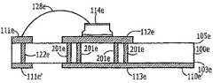
図1A〜E、2、3、4A〜Cおよび5の実施形態を参照すると、基板(サブマウントとも呼ぶ。)100a〜kはそれぞれ、図示のように、それぞれ上面105a〜kおよび下面103a〜kを有することができる。基板100a〜kはそれぞれ、プリント回路板(PCB)基板、アルミニウムブロック(block)基板、アルミナ基板、窒化アルミニウム基板、サファイア基板および/またはシリコン基板、ならびに/または、例えば米ミネソタ州ChanhassenのThe Bergquist Company社から入手可能なT−Cladサーマルクラッドで断熱された基板材料など、他の適当な基板材料を含むことができる。PCB基板には、標準FR−4 PCB、金属コア(metal−core)PCB、フレックステープ、および/または他の任意のタイプのプリント回路板を含めることができる。 Referring to the embodiments of FIGS. 1A-E, 2, 3, 4A-C and 5, substrates (also referred to as submounts) 100a-k, respectively, have upper and
図1A〜E、2、3、4A〜Cおよび5に示されているように、各基板100a〜kの上面105a〜kに、パターニングされた金属形体(1つまたは複数)を形成することができる。パターニングされた金属形体(1つまたは複数)には、熱伝導層(1つまたは複数)112a〜k、(図3に示されている)メニスカス(meniscus)制御形体(1つまたは複数)303および/または304、(図3に示されている)ワイヤボンドパッド(1つまたは複数)305、ならびに/あるいは電極110a〜kおよび/または111a〜kを含めることができる。基板100a〜kの上面105a〜k上の導電形体は例えばめっき工程を使用して形成することができる。めっき工程を使用して、基板上に薄い金属膜または厚い金属膜をめっきすることができる。一般的なめっき工程では、基板上に、チタン接着層および銅シード(seed)層を逐次的にスパッタリングすることができる。次いで、銅シード層上に、約75ミクロンの銅をめっきすることができる。あるいは、接着層およびシード層を例えば金属マスクを使用してスパッタリングして、所望のパターンを形成することもできる。めっき工程を使用して、基板を貫通する導電金属ビアを形成することもできる。代替として、堆積させた金属膜を標準リソグラフィ工程によりパターニングして、基板上に所望のパターンを有する金属形体を形成することもできる。 As shown in FIGS. 1A-E, 2, 3, 4A-C and 5, forming patterned metal feature (s) on
図3に示された本発明のいくつかの実施形態では、第1および第2のメニスカス制御形体303および304を、熱伝導層112gおよび/またはワイヤボンドパッド305とは異なる材料から形成することができる。例えば、メニスカス制御形体303および304は、例えばポリイミドを含むはんだマスク材料などのポリマーを含むことができる。例えばポリイミドなどのポリマーは、メニスカス制御形体として使用するのに適した材料となりうる。なぜならば、ポリイミドの表面エネルギーは比較的低く、このことは改良されたメニスカス制御特性を提供することができるからである。 In some embodiments of the present invention illustrated in FIG. 3, the first and second meniscus control features 303 and 304 may be formed from a different material than the thermally
熱伝導層112a〜kの水平寸法(基板に平行な方向の寸法)および厚さは、使用される材料の熱拡散特性に基づいて変更してもよい。熱拡散は、熱伝導層112a〜kの直径または(基板の表面に平行な方向の)幅が、LED源114a〜kの1つまたは複数の縁から、LED源114a〜kの幅の少なくとも半分の距離だけ延在するときに増大させることができ、本発明のいくつかの実施形態では、少なくともLED源114a〜kの幅と同じ距離だけ延在するときに増大させることができる。さらに、熱伝導層112a〜kは、LED114a〜kの縁からさらに、熱伝導層の厚さの2倍よりも大きい距離だけ延在することができる。本発明のいくつかの実施形態によれば、熱伝導層112a〜kは、(銅、アルミニウム、金、スズ、スズ−銀および/または銅−スズなどの)金属層、(窒化アルミニウムなどの)セラミック層、および/または(炭化ケイ素などの)半導体材料層を含むことができる。熱伝導層112a〜kとして銅層が設けられる場合には、銅の熱伝導層(1つまたは複数)112a〜kの直径または(基板の表面に平行な方向の)幅と(基板の表面に垂直な方向の)厚さの比が、少なくとも約25から約140の範囲にあるように、銅の熱伝導層(1つまたは複数)を構成することができる。熱伝導層112a〜kとしてアルミニウム層が設けられる場合には、アルミニウム熱伝導層(1つまたは複数)112a〜kの直径または(基板の表面に平行な方向の)幅と(基板の表面に垂直な方向の)厚さの比が、少なくとも約7から約50の範囲にあるように、アルミニウムの熱伝導層(1つまたは複数)を構成することができる。 The horizontal dimension (dimension in the direction parallel to the substrate) and thickness of the heat
各基板100a〜kの上面105a〜k上に、1つまたは複数の電極110a〜kおよび/または111a〜kを形成することができる。さらに、図1C〜E、2および3に示されているように、各基板100c〜gの下面103c〜g上に、1つまたは複数の下電極110c’〜g’および/または111c’〜g’を形成することができる。1つまたは複数の導電ビア122c〜gが、1つまたは複数の下電極110c’〜g’および/または111c’〜g’を、各基板100c〜gの上面105c〜g上の様々な形体に接続することができる。例えば、導電ビア122c〜gおよび/または122c’〜g’のうちの1つが、電極110c〜gおよび/または111c〜gを、それぞれの下電極110c’〜g’および/または111c’〜g’に電気的に接続することができる。これに応じて、基板100c〜gの上面105c〜g上に形成される各導電形体は、同じ材料から形成することができる。例えば、導電性形体は、めっき工程を使用して堆積させた銅を含むことができる。 One or
本発明の他のいくつかの実施形態では、いくつかの導電形体が追加の金属を含んでもよい。例えば、熱伝導層(1つまたは複数)112a〜kを、それぞれのLEDチップ114a〜kを取り付けるのにより適当なものとするために、熱伝導層(1つまたは複数)112a〜kに対して、追加の金属および/または他の材料によるめっき及び/又はコーティングを施すことができる。例えば、熱伝導層(1つまたは複数)112a〜kを、例えば追加の接着層、接合層、反射層、ダイ接着(die attach)パッド層および/または障壁層(図示せず)などの追加の層でめっきすることができる。これらの層を熱伝導層に追加することができ、これらの追加の層も熱伝導性とすることができる。代替として、LED114a〜kとそれぞれの熱伝導層112a〜kとの間の熱抵抗を低下させ、かつ/またはボイドの発生を低減させるために、Au/Snはんだペーストの代わりにフラックスを使用して、直接ダイ接着を実行することができる。直接ダイ接着は、ESD保護用の別個のツェナーデバイスをLEDシステムの他の領域で使用することを可能にする。LED(1つまたは複数)114a〜kおよびそれぞれの熱伝導層(1つまたは複数)112a〜kを、垂直、平面および/またはフリップチップLEDとの結合(coupling)を提供するように構成することができる。 In some other embodiments of the present invention, some conductive features may include additional metals. For example, in order to make the thermal conductive layer (s) 112a-k more suitable for attaching the
図1A〜Eに示されているように、それぞれの基板100a〜eの上面(主表面)105a〜e上に、熱伝導層112a〜eを形成することができる。図1C〜1Eに示されているように、それぞれの基板103C〜Eの下面(副表面)103c〜eにさらに、第2の熱伝導層113c〜eを形成することができる。図1D〜Eに示されているように、第1の熱伝導層(1つまたは複数)112d〜eと第2の熱伝導層(1つまたは複数)113d〜eとの間に、熱伝導ビア201d〜eを熱的に結合することができる。熱伝導ビア201d〜eは、第1の熱伝導層(1つまたは複数)112d〜eと第2の熱伝導層(1つまたは複数)113d〜eとの間の熱結合を向上させるため、基板100d〜eを貫通して延在することができる。基板を貫通するそれぞれのビアの(基板の上面または下面から見た)外形は、円、正方形、多角形など任意の形状をとることができる。それぞれの熱伝導ビア201d〜eは、それぞれの熱伝導層112の任意の部分から延在することができる。本発明のいくつかの実施形態によれば、熱伝導を増大させるために、熱伝導ビア201d〜eを、LED114d〜eと第2の熱伝導層113d〜eとの間に形成することができる。本発明の他のいくつかの実施形態によれば、LED114d〜eと熱伝導層112d〜eとの間の機械的結合を向上させるため、熱伝導ビア201d〜eを、それぞれのLED114d〜eから間隔を置いて配置する(または横方向にオフセットする)ことができる。例えば、熱伝導ビア201d〜eがない部分の熱伝導層112d〜eは、LED114d〜eとの機械的結合を向上させるより平らな表面を提供することができる。 As shown in FIGS. 1A to 1E, heat
熱伝導層112a〜eおよび/または113c〜eは薄膜技術を使用して形成することができるため、本発明のいくつかの実施形態によれば、図1A、1Cおよび/または1Dに示されているように、第1および第2の熱伝導層112a〜eおよび/または113c〜eを、電極110a〜eおよび/または111a〜eから電気的に分離することができる。この電気的な分離は、例えば、熱伝導層(1つまたは複数)の材料(1種または数種)と電極の材料(1種または数種)とを異なるものにすることができるように提供される。図1A〜Eに示されているように、ワイヤボンド128a〜eを使用して、LED114a〜eとそれぞれの電極111a〜eとの間の電気的結合を与えることができる。図1Aおよび1C〜Dに示されているように、ワイヤボンド128a’および128c’〜d’が、LED114aおよび114c〜dとそれぞれの電極110aおよび110c〜dとの間の電気的結合を提供することができる。図1Bに示されているように、熱伝導層112bと電極110bは、導電性かつ熱伝導性の材料の連続層/パターニングされた層として設けることができる。例えば、熱伝導材料のパターニングされた層が、熱伝導層112b、電極110bおよびこれらの間の導電トレースを提供することができる。図4A〜Bに示されているように、熱伝導層(1つまたは複数)112h〜iを、それぞれの電極(1つまたは複数)111h〜iに、導電トレース(1つまたは複数)402h〜iを介して電気的に結合することができる。図1Eに示されているように、第2の熱伝導層113eを電極110e’に電気的に結合することができる。図1Eに示されているように、導電性かつ熱伝導性のビア201eを介して、第1の熱伝導層112eを、基板100eの下面103eの電極110e’に電気的に結合することができる。 As the thermal
図1A〜Eには示されていないが、例えば図2および3に示されているようなレンズおよび/または反射デバイスと共に、図1A〜Eの構造を使用することができる。さらに、図2の構造を図3のレンズと共に使用することもでき、かつ/または図3の構造を図2のレンズと共に使用することもできる。さらに、(例えば図1A〜E、2、3、4A〜Bおよび5に関して論じた)本発明の実施形態による、熱伝導層、熱伝導/導電ビア、LED、電極および/または基板を備える構造を、例えば特許文献19および20で論じられているLEDパッケージングの追加の要素と共に使用することもできる。これらの特許文献の開示は、その全体が本明細書に記載されているかのように参照によって本明細書に組み込まれる。 Although not shown in FIGS. 1A-E, the structure of FIGS. 1A-E can be used with lenses and / or reflective devices, such as those shown in FIGS. 2 and 3, for example. Furthermore, the structure of FIG. 2 can be used with the lens of FIG. 3 and / or the structure of FIG. 3 can be used with the lens of FIG. Furthermore, a structure comprising a heat conducting layer, a heat conducting / conducting via, an LED, an electrode and / or a substrate according to an embodiment of the invention (eg discussed with respect to FIGS. 1A-E, 2, 3, 4A-B and 5). It can also be used with additional elements of LED packaging as discussed, for example, in US Pat. The disclosures of these patent documents are hereby incorporated by reference as if set forth in full herein.
より具体的には、図1AのLEDパッケージは、LED114aと基板100aとの間に熱伝導層112aを備えることができ、熱伝導層112aは、LED114aの縁から、LED114aの幅の半分を超える距離だけ延在することができ、本発明のいくつかの実施形態では、LED114aの幅を超える距離だけ延在することができる。さらに、LEDを、両方の電極(すなわちカソードとアノード)が基板100aとは反対側のLED114aの表面上にある水平LED(horizontal LED)とすることができる。LED114aと電極111aおよび110aとの間の電気的結合は、ワイヤボンド128aおよび128a’が提供することができる。したがって、LED114aとは反対側の基板100aの下面103aには電気接続がないようにすることができる。動作中、LEDからの熱を、熱伝導層112aを通して基板100a内へ拡散させることができる。熱伝導層112aは、銅などの導電性かつ熱伝導性の材料を含むことができる。さらに、基板100aから熱が運び去られるように、基板100aの裏面103aをヒートシンクに熱的に結合し、かつ/または(プリント回路板などの)他の基板の熱伝導部分に熱的に結合することができる。 More specifically, the LED package of FIG. 1A can include a thermally
図1BのLEDパッケージは、LED114bと基板100bとの間に熱伝導層112bを備えることができ、熱伝導層112bは、LED114bの縁から、LED114bの幅の半分を超える距離だけ延在することができ、本発明のいくつかの実施形態では、LED114bの幅を超える距離だけ延在することができる。さらに、LEDを、LEDの電極(すなわちカソードとアノード)が互いにLED114bの反対側の表面にある垂直LED(vertical LED)とすることができる。LED114bの第1の電極と電極111bとの間の電気的結合は、ワイヤボンド128bが与えることができる。LED114bの第2の電極は、熱伝導層112bに直接に結合することができる。図1Bにさらに示されているとおり、第2のワイヤボンドが不要になるように、熱伝導層112bおよび電極110bならびにこれらの間のトレースを、導電性かつ熱伝導性の同じ材料層から形成することができる。図1Aの構造と同様に、LED114bとは反対側の基板100bの下面103bには電気接続がないようにすることができる。動作中、LED114bからの熱を、熱伝導層112bを通して基板100b内へ拡散させることができる。熱伝導層112aは、銅などの導電性かつ熱伝導性の材料を含むことができる。さらに、基板100bから熱が運び去られるように、基板100bの裏面103bをヒートシンクに熱的に結合し、かつ/または(プリント回路板などの)他の基板の熱伝導部分に熱的に結合することができる。LED114bが水平LEDである場合には、熱伝導層112bとは反対側のLED114bの表面上の第2の電極と熱伝導層112bとの間に第2のワイヤボンドを形成することができる。 The LED package of FIG. 1B can include a thermally
図1CのLEDパッケージは、LED114cと基板100cとの間に熱伝導層112cを備えることができ、熱伝導層112cは、LED114cの縁から、LED114cの幅の半分を超える距離だけ延在することができ、本発明のいくつかの実施形態では、LED114cの幅を超える距離だけ延在することができる。さらに、このLEDを、LEDの電極(すなわちカソードとアノード)が互いにLED114cの反対側の表面にある垂直LEDとすることができる。LED114cの第1の電極と電極111cとの間の電気的結合は、ワイヤボンド128cが与えることができる。さらに層112cを導電性とすることができ、LED114cの第2の電極を、熱伝導性かつ導電性の層112cに直接に結合することができ、ワイヤボンド128c’が、熱伝導層112cと電極110cの間の電気的結合を提供することができる。代替として、第2のワイヤボンドが不要になるように、図1Bに関して上で論じたように、熱伝導層112cと電極110cの間に導電トレースを形成することもできる。 The LED package of FIG. 1C can include a thermally
図1Cでは、基板100cの裏面103cに第2の熱伝導層113cを配置して、基板100cからヒートシンクおよび/または(プリント回路板などの)別の回路板の熱伝導部分への熱の結合を強化することができる。動作中、LED114cからの熱を、熱伝導層112cを通して基板100cおよび第2の熱伝導層113c内へ拡散させることができる。熱伝導層112cおよび113cは、それぞれ銅などの熱伝導材料を含むことができる。さらに、基板100cから熱が運び去られるように、基板100cの裏面103cをヒートシンクに熱的に結合し、かつ/または(プリント回路板などの)別の基板の熱伝導部分に熱的に結合することができる。LED114cが水平LEDである場合には、熱伝導層112cとは反対側のLED114cの表面上の第2の電極と電極110cとの間に第2のワイヤボンド128c’を形成することができる。 In FIG. 1C, a second thermally
図1Cにさらに示されているように、基板100cの裏面103cに2次電極(secondary electrode)111c’および110c’を配置することができ、導電ビア122cおよび122c’を介して、2次電極111c’および110c’を、基板100cの表面105cの電極111cおよび110cに電気的に結合することができる。したがって、2次電極111c’および110c’がプリント回路板への電気的結合を状態で、プリント回路板上に基板100cを取り付けることができる。代替として、他の基板への電気的結合が、電極111cおよび110cに直接に提供される場合には、導電ビア122cおよび122c’ならびに2次電極111c’および110c’を省くことができる。 As further shown in FIG. 1C, secondary electrodes 111c ′ and 110c ′ can be disposed on the
さらに、本発明のいくつかの実施形態によれば、図1Cに関して上で論じた導電ビアおよび2次電極を、図1Aおよび/または1Bの構造に適用することができる。例えば、図1Aの基板100aを貫通するそれぞれの導電ビアを使用して、基板100aの裏面103a上の2次電極を電極111aおよび110aに電気的に結合することができる。同様に、図1Bの基板100bを貫通するそれぞれの導電ビアを使用して、基板100bの裏面103b上の2次電極を電極111bおよび110bに電気的に結合することができる。 Further, according to some embodiments of the present invention, the conductive vias and secondary electrodes discussed above with respect to FIG. 1C can be applied to the structure of FIGS. 1A and / or 1B. For example, each conductive via that passes through the
図1DのLEDパッケージは、LED114dと基板100dとの間に熱伝導層112dを備えることができ、熱伝導層112dは、LED114dの縁から、LED114dの幅の半分を超える距離だけ延在することができ、本発明のいくつかの実施形態では、LED114dの幅を超える距離だけ延在することができる。さらに、このLEDを、電極(すなわちカソードとアノード)が基板100dとは反対側のLED114dの表面にある水平LEDとすることができる。LED114dの電極と電極111dおよび110dとの間の電気的結合は、ワイヤボンド128dおよび128d’が提供することができる。 The LED package of FIG. 1D can include a thermally conductive layer 112d between the
図1Dでは、基板100dの裏面103d上に第2の熱伝導層113dを設けて、基板100dからヒートシンクおよび/または(プリント回路板などの)別の回路板の熱伝導部分への熱の結合を強化することができる。さらに、熱伝導ビア201dが、第1の熱伝導層112dと第2の熱伝導層113dとの間の熱結合を向上させることができる。動作中、LED114dからの熱を、熱伝導層112dおよび熱伝導ビア201dを通して、第2の熱伝導層113dへ放拡散させることができる。熱伝導層112dおよび113dならびに熱伝導ビア201dはそれぞれ、銅などの熱伝導材料を含むことができる。さらに、基板100dから熱が運び去られるように、基板100dの裏面103dをヒートシンクに熱的に結合し、かつ/または(プリント回路板などの)別の基板の熱伝導部分に熱的に結合することができる。 In FIG. 1D, a second thermally conductive layer 113d is provided on the
LED114dが垂直LEDである場合には、LED114dの第2の電極を熱伝導層112dに直接に結合することができ、熱伝導層112dと電極110dとの間の電気的結合は、ワイヤボンド128d’が提供することができる。代替として、第2のワイヤボンドが不要になるように、図1Bに関して上で論じたように、熱伝導層112dと電極110dとの間に導電トレースを形成することもできる。 If the
図1Dにさらに示されているように、基板100dの裏面103dに2次電極111d’および110d’を設けることができ、導電ビア122dおよび122d’を介して、2次電極111d’および110d’を、基板100dの表面105d上の電極111dおよび110dに電気的に結合することができる。したがって、2次電極111d’および110d’がプリント回路板への電気的結合を与える形で、プリント回路板上に基板100dを取り付けることができる。代替として、別の基板への電気的結合が、電極111dおよび110dに直接に提供される場合には、導電ビア122dおよび122d’ならびに2次電極111d’および110d’を省くことができる。 As further shown in FIG. 1D,
図1EのLEDパッケージは、LED114eと基板100eとの間に熱伝導層112eを備えることができ、熱伝導層112eは、LED114eの縁から、LED114eの幅の半分を超える距離だけ延在することができ、本発明のいくつかの実施形態では、LED114eの幅を超える距離だけ延在することができる。さらに、このLEDを、LEDの電極(すなわちカソードとアノード)が互いにLED114eの反対側の表面にある垂直LEDとすることができる。LED114eの第1の電極と電極111eとの間の電気的結合は、ワイヤボンド128eが提供することができる。LED114eの第2の電極は、熱伝導層112eに電気的かつ機械的に結合することができる。 The LED package of FIG. 1E can include a thermally
図1Eでは、基板100eの裏面103eに第2の熱伝導層113eを設けて、基板100eからヒートシンクおよび/または(プリント回路板などの)別の回路板の熱伝導部分への熱の結合を強化することができる。さらに、熱伝導ビア201eが、第1の熱伝導層112eと第2の熱伝導層113eとの間の熱結合を向上させることができる。動作中、LED114eからの熱を、熱伝導層112eおよび熱伝導ビア201eを通して、第2の熱伝導層113eへ拡散させることができる。熱伝導層112eおよび113eならびに熱伝導ビア201eはそれぞれ、銅などの熱伝導材料を含むことができる。さらに、基板100eから熱が運び去られるように、基板100eの裏面103eをヒートシンクに熱的に結合し、かつ/または(プリント回路板などの)別の基板の熱伝導部分に熱的に結合することができる。LED114eが水平LEDである場合には、第2のワイヤボンドを使用して、LED114eの第2の電極を熱伝導層112eに結合することができる。 In FIG. 1E, a second thermally conductive layer 113e is provided on the
図1Eにさらに示されているように、基板100eの裏面103e上に2次電極111e’および110e’を設けることができる。導電ビア122eを介して、2次電極111e’を、基板100eの表面105e上の電極111eに電気的に結合することができる。2次電極110e’は、基板100eの裏面103e上のトレースを介して第2の熱伝導層113eに電気的に結合することができる。したがって、LED114eと電極110e’との間の電気的結合は、第1の熱伝導層112e、熱伝導トレース201eおよび第2の熱伝導層113eを介して提供することができる。本発明のいくつかの実施形態によれば、2次電極110e’と第2の熱伝導層113eを、導電性かつ熱伝導性の同じ層の部分として形成することができ、かつ/または別の基板への電気的結合を、第2の熱伝導層113eに直接に提供することができる。したがって、2次電極111e’および110e’がプリント回路板への電気的結合を提供する形で、プリント回路板上に基板100eを取り付けることができる。 As further shown in FIG. 1E,
図2を参照する。本発明のいくつかの実施形態によれば、LED114fの周りに、金属および/または反射カップ(またはリング(ring))212を設けることができ、反射カップまたはリング212の内側に、予め形成されたレンズ210を接着材211を使用して固定することができる。リング212と基板100fとの間、および/またはリング212と基板100f上の(電極110fおよび/または111fなどの)他の層との間に、電気絶縁材料213を配置することができる。基板100fを貫通して第2の熱伝導層113fまで延在する熱伝導ビア201fを使用して、第1の熱伝導層112fと第2の熱伝導層113fとを熱的に結合することができる。図2にさらに示されているように、熱伝導層112fおよび113fならびに熱伝導ビア201fを含む一体化(integrated)熱拡散システムを、LED114fの電極から、ならびに/あるいは電極110f、110f’、111fおよび/または111f’から電気的に分離することができる。LED114fの電極は、ワイヤボンド128fおよび128f’によって、電極110Aおよび/または111Aに電気的に結合することができる。レンズおよび反射カップは、例えば特許文献19に論じられているように作製することができる。この特許文献の開示は、その全体が参照によって本明細書に組み込まれる。 Please refer to FIG. According to some embodiments of the present invention, a metal and / or reflective cup (or ring) 212 may be provided around the
図3に示されているように、発光デバイスアセンブリは、本発明のいくつかの実施形態に基づく1つまたは複数の封止領域を備えることができる。より具体的には、基板100g上の第1のメニスカス制御形体(meniscus control feature)303が熱伝導層112gを取り囲んで、基板100gの上面105gの第1のメニスカス制御形体303の周囲の内側に、封止材301を閉じ込める領域を画定することができる。第2のメニスカス制御形体304が領域301を取り囲むことができ、第2のメニスカス制御形体304が領域301を取り囲み、第1のメニスカス制御形体303と共に、第1の封止領域301を取り囲む基板100gの上面105gに、レンズ材料302を閉じ込める環状(またはリング形)領域を画定することができる。封止材301は、第1のメニスカス制御形体303によって閉じ込められた液体として分配(dispense)し、次いで硬化させることができる。次いでレンズ材料302を、第2のメニスカス制御形体304によって閉じ込められた液体として分配し、次いで硬化させることができる。封止材301および/またはレンズ材料302はエポキシ材料(1種または数種)とすることができる。 As shown in FIG. 3, the light emitting device assembly may comprise one or more sealing regions according to some embodiments of the present invention. More specifically, a first meniscus control feature 303 on the
図3に示されているように、レンズ材料302は封止材301を取り囲み、包囲することができる。レンズ材料302は上で論じたように環状とすることができるが、第1のメニスカス制御形体303および第2のメニスカス制御形体304の形状、ならびに分配される封止材および/またはレンズ材料の体積に応じた他の形状に従ってレンズ材料302を設けることもできる。例えばレンズ材料は卵形の周囲を有することができる。ある形体がある領域を「取り囲む」ためには、形体が、その領域の周りに途切れなく形成される必要はないことが理解される。図は連続するメニスカス制御形体を示しているが、メニスカス制御形体が、その形体のメニスカス制御機能に影響を及ぼさない空隙またはボイドを含むことが可能である場合もある。さらに、形体は円形である必要はなく、楕円形、多角形など他の2次元形状として提供することもできる。 As shown in FIG. 3, the
図3にさらに示されているように、基板100gの上面105gの第2のメニスカス制御形体304によって取り囲まれたレンズ領域内に、ワイヤボンドパッド305および305’を形成することができる。導電ビア122gの1つが、ワイヤボンドパッド305および/または305’を、それぞれの下電極111g’および/または110g’に電気的に結合することができる。導電ビア122gのうちの別のものが、下電極111g’および/または110g’を、基板100gの上面105gのそれぞれの電極111gおよび/または110gに電気的に結合することができる。別の代替実施形態(図示せず)では、垂直LEDの下面を、下電極111g’および/または110g’の一方に電気的に結合することができるように、導電性かつ熱伝導性のビア201gが、熱伝導層112gを下電極111g’および/または110g’に電気的に結合することができ、それによってワイヤボンド128gおよび/または128g’の一方を排除することができる。さらに、図1A〜Eに示されているようにLED114gが露出するように、LED114g、ビア122g、122g’および201g、熱伝導層112gおよび113g、ワイヤボンドパッド305および305’、ならびに電極111g、111g’、110gおよび110g’を備え、封止材301およびレンズ材料302を備えない構造を設けることができる。代替として、図3の構造は、封止材およびレンズ材料の代わりに図2の反射器およびレンズ構造を備えることができる。 As further shown in FIG. 3,
レンズは、例えば特許文献21および20で論じられているように作製することができる。これらの特許文献の開示はともに、その全体が参照によって本明細書に組み込まれる。 The lens can be made, for example, as discussed in US Pat. The disclosures of these patent documents are both incorporated herein by reference in their entirety.
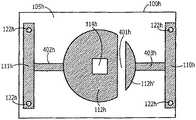
本発明のいくつかの実施形態によれば、熱伝導層(1つまたは複数)112a〜gは平面図において円形とすることができ、または卵形、多角形など他の形状を有することができる。一例として、熱伝導層(1つまたは複数)112a〜gを、図4A〜Cに示されているように実質的に円形とすることができる。実質的に円形の形状は、例えば、効率的に熱を拡散させると共に、LED源114a〜gから正方形または長方形の熱伝導層の角までの距離がより長いことが原因として生じうる(加熱による)不必要な膨張を低減させることができる。 According to some embodiments of the present invention, the thermally conductive layer (s) 112a-g can be circular in plan view, or can have other shapes such as oval, polygonal, etc. . As an example, the thermally conductive layer (s) 112a-g can be substantially circular as shown in FIGS. The substantially circular shape can arise, for example, due to a longer distance from the
図4Aの平面図に示されているように、実質的に円形の熱伝導層112h上にLED114hを配置することができる。より具体的には、熱伝導層112hは、熱伝導層112hの部分112h’を電気的に分離する隙間(gap)401hを有することができる。熱伝導層112hと電極111hとの間の電気的結合はトレース402hが与えることができ、部分112h’と電極110hとの間の電気的結合はトレース403hが与えることができる。(その上面に両方の電極を有する)水平LED114hでは、熱伝導層112hの主要部分とLED114hとの間の電気的結合を第1のワイヤボンドが与えることができ、部分112h’とLED114hとの間の電気的結合を第2のワイヤボンドが与えることができる。部分112h’は、熱伝導層112hの熱拡散能力をあまり低減させることなく、ワイヤボンド接続のための比較的大きな面積を提供することができる。(反対側の表面に電極を有する)垂直LED114Hでは、LED114hの第1の表面を熱伝導層112hの主要部分に(例えば、はんだを使用して)電気的かつ機械的に接合することができ、(熱伝導層とは反対側の)第2の表面と熱伝導層の部分112h’との電気的結合は、ワイヤボンドが提供することができる。 As shown in the plan view of FIG. 4A, the
本発明の他の実施形態によれば、(トレース402hおよび/または403hの一方または両方を排除することができるように)熱伝導層112hを、電極111hおよび110hから電気的に分離することができる。トレース402hおよび/または403hがない場合、LED114hと電極111hおよび/または110hとの間の電気的結合は、ワイヤボンドが提供することができる。さらに、例えば図1C、1Dおよび1Eに示されているように、熱伝導層112hとは反対側の基板100hの表面に第2の熱伝導層(図示せず)を設けることができ、かつ/または例えば図1Dおよび1Eに示されているように、基板110hを貫通する熱伝導ビアが、基板100hの両側の熱伝導層間の熱結合を提供することができる。 According to other embodiments of the present invention, the thermally
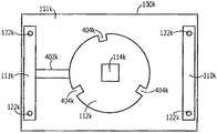
熱膨張による応力/ひずみを低減させるため、図4Bに示されているように、実質的に円形の熱伝導層112iに切欠き(notch)404iを形成することができる。したがって、LED114iが発生した熱を、比較的に大きな熱伝導層112i全体から放散させると共に、熱伝導層全体の熱応力/ひずみを低減させることができる。図4Bに示されているように、切欠き404iは、熱伝導層112iの周囲部分に沿って間隔を置いて配置することができる。さらに、LED114iから熱伝導層112iの縁に向かう熱流のインピーダンスを低減させるため、切欠き112iは、LED112iに向かって半径方向に延在することができる。電極111iおよび110i、トレース402iおよび403i、導電ビア122iおよび基板100iは、図4Aの対応する要素に関して上で論じたように設けることができ、かつ/または機能することができる。 In order to reduce stress / strain due to thermal expansion, a notch 404i can be formed in the substantially circular thermally conductive layer 112i, as shown in FIG. 4B. Therefore, the heat generated by the
図4Aおよび4Bにさらに示されているように、図4A〜Bの電気的に分離する隙間401h〜iは、熱伝導層をめっきするときにはんだマスクを使用することによって、または熱伝導層のめっきに続いて(例えばフォトリソグラフィマスクおよびエッチング操作を使用して)熱伝導層をパターニングすることによって形成することができる。この隙間401hまたは401iは、実質的に円形の熱伝導層のカソード部分とアノード部分を電気的に分離すると共に、大幅な熱拡散を提供することができる。導電トレース402h〜iおよび/または403h〜iは、熱伝導層の部分112h〜iおよび/または112h’〜i’を電極110h〜iおよび/または110h〜iに電気的に結合することができる。 As further shown in FIGS. 4A and 4B, the electrically isolating
本発明のさらなる実施形態によれば、図4Cに示されているように、実質的に円形の熱伝導層112kを、電極111kおよび/または110kの一方または両方から電気的に分離することができる。さらに、熱伝導層112kから図4Aおよび4Bの隙間を省くことができ、切欠き404kを、熱伝導層112kの周囲部分に沿って実質的に等間隔に配置することができる。例えば図4Cに示された3つの切欠きでは、切欠き404kを、実質的に円形の熱伝導層112kの周囲に約120度間隔で配置することができる。4つの切欠きでは、切欠きを、実質的に円形の熱伝導層の周囲に約90度間隔で配置することができる。 According to a further embodiment of the invention, as shown in FIG. 4C, the substantially circular
さらに、LED114kから熱伝導層112kの縁に向かう熱流のインピーダンスを低減させるため、切欠き112kは、LED112kに向かって半径方向に延在することができる。電極111kおよび110k、トレース402k、導電ビア122kおよび基板100kは、図4A〜Bの対応する要素に関して上で論じたように設けることができ、かつ/または機能することができる。一例として、LEDを、熱伝導層に電気的かつ機械的に接合された(例えば、はんだ付けされた)第1の表面を有する垂直LEDとすることができ、LED114Kの第2の表面と電極110kとの間の電気的結合は、ワイヤボンドが与えることができる。代替として、LED114kを、LED114kの第1の部分と熱伝導層112kとの間の電気的結合を与える第1のワイヤボンドと、LEDの第2の部分と電極110kとの間の電気的結合を与える第2のワイヤボンドとを有する水平LEDとすることができる。 Furthermore, the
図4A〜Cの熱伝導層112h、112iおよび/または112kはいずれも、基板100h、100iおよび/または100kの反対側の表面に配置された第2の熱伝導層に、例えば熱伝導ビアを使用して電気的に結合することができる。本発明のいくつかの実施形態によれば、LEDを接合してもよい表面をより平坦にするために、このような熱伝導ビアを、LED114h、114iおよび/または114kからずらして配置することができる。本発明の他の実施形態によれば、LEDと基板の反対側の表面上の第2の熱伝導層との間に、1つまたは複数の熱伝導ビアを直接に設けてもよい。さらに、図4A〜Cに関して上で論じた熱伝導層112h、112iおよび/または112kのパターンのうちの任意のものを、図1A〜E、2、3および/または5に関して本明細書で論じた熱伝導層に対して使用することができる。さらに、実質的に円形の熱伝導層112h、112iおよび/または112kはそれぞれ、それぞれのLED114h、114iおよび/または114kの縁から、LEDの幅の半分を超える距離だけ延在することができ、本発明のいくつかの実施形態では、LEDの幅を超える距離だけ延在することができる。 Any of the thermally
本発明のさらなる実施形態は、図5に示された3チップ直列配置(layout)などのように、同一基板上に複数のLEDを備えることができる。図5では、3つのLED114j、114j’および114j”を電気的に直列に結合することができる。図解の目的上、LED114j、114j’および114j”はそれぞれ、図1Aに関して上で論じた構成と同様の構成で設けることができる。電極111jおよび/または110jをそれぞれの導電トレース501jに電気的に結合することができ、LED114j、114j’および/または114j”間に追加の導電トレースを形成することができる。図5に示されているように、LED114j、114j’および114j”はそれぞれ、それぞれのワイヤボンド対128j、128j’および/または128j”を使用してトレースに電気的に結合することができる。図5に示されているように、熱伝導層112j、112j’および/または112j”を、電極110jおよび/または111jならびに/あるいはトレース501jから電気的に分離することができる。 Further embodiments of the present invention can include multiple LEDs on the same substrate, such as the three-chip layout shown in FIG. In FIG. 5, three
図5では各LEDに対して一対のワイヤボンドが設けられているが、LED間に直接にワイヤボンド接続を提供することによって、ならびに/あるいは電極111jおよび/または110jに直接にワイヤボンド接続を提供することによって、いくつかのワイヤボンドおよび/またはトレースを減らすことができる。図5にさらに示されているように、それぞれのLEDへの両方の電気的結合が基板100jとは反対側のLEDの表面に設けられた水平LEDを使用することができる。垂直LEDでは、LED114j、114j’および/または114j”からそれぞれの熱伝導層112j、112j’および/または112j”まで第1の電気的結合を形成することができ、基板100jとは反対側のLED114j、114j’および/または114j”の表面への第2の電気的結合は、ワイヤボンドを使用して提供することができる。 Although a pair of wire bonds are provided for each LED in FIG. 5, providing a wire bond connection directly between LEDs and / or providing a wire bond connection directly to
図1C〜E、2および3に関して上で論じたのと同様に、熱伝導層112j、112j’および/または112j”の反対側の基板100jの裏面に第2の熱伝導層を配置することができる。例えば、各第1の熱伝導層112j、112j’および/または112j”に対して別個の第2の熱伝導層を設けることができる。基板100jの裏面に電気接続が提供されない場合、基板100jの裏面103j全体に、連続する第2の熱伝導層505を形成することができる。さらに、1つまたは複数の熱伝導層112j、112j’および/または112j”と基板100jの裏面103jのこのような任意の第2の熱伝導層との間に、基板100jを貫通する熱伝導ビアを形成することができる。 As discussed above with respect to FIGS. 1C-E, 2 and 3, placing a second thermally conductive layer on the back surface of the substrate 100j opposite the thermally
さらに、この一連のLEDチップ114j、114j’、114j”を、(ツェナーダイオードなどの)ESD(静電放電(electrostatic discharge))保護チップ502に結合することもできる。本発明の実施形態に基づく一体化熱拡散は、薄膜/直接接合技術を使用するのにより好都合な条件を提供することができ、単一のフォームファクタ(form factor)の小さいLEDパッケージ上に複数のLEDチップを配置することを可能にする。本発明のいくつかの実施形態によれば、このようなマルチチップアセンブリが発生した熱を、LEDからより効果的に運び去ることができる。 Further, this series of
図4A〜Cに関して上で論じたのと同様に、熱伝導層112j、112j’および/または112j”はそれぞれ実質的に円形とすることができ、かつ/あるいはその中に切欠きを含むことができる。さらに、図2および/または3に関して上で論じたのと同様に、LED114j、114j’および/または114j”に対して、反射カップ、予め形成されたレンズ、メニスカス制御形体および/または液体分配/硬化レンズを設けることができる。 As discussed above with respect to FIGS. 4A-C, each of the thermally
したがって、本発明のいくつかの実施形態に基づく熱伝導層(例えば上で論じた熱伝導層112a〜k)は、熱伝導層が形成された基板(例えば上で論じた基板100a〜k)と一体の熱拡散器を提供することができる。LEDをより高い電力、例えば最大5ワットの電力で動作させることができるように、LED(例えばLED114a〜k)から基板および/またはヒートシンク内への熱の熱輸送を改良することができる。本発明のいくつかの実施形態に基づく熱伝導層は、高導電金属の薄膜処理およびフォトリソグラフィパターニングを使用して形成することができる。本発明のいくつかの実施形態に基づく熱伝導層は、直接フラックスダイ接着(direct flux die attach)および/またはESD保護用の別個のツェナーダイオードの取付けを可能にする。 Thus, the thermally conductive layers (eg, the thermally
より具体的には、図1A〜E、2、3、4A〜Cおよび5に関して上で論じた熱伝導層112a〜kは例えば、ニッケル、銅、金および/または銀などの金属(1種または数種)の1つまたは複数の層をめっきし、スパッタリングし、かつ/または蒸着させることによって形成することができる。基板を通しての熱輸送を促進するため、基板を貫通する穴の中の銅などの高熱伝導材料を使用して、熱伝導ビア(例えば導電ビア201d〜g)を形成することができる。さらに、熱伝導層112a〜kは、例えば金/スズはんだペーストの代わりにフラックスを使用して、LED114a〜kの直接ダイ接着を可能にすることができる。したがって、LEDと熱伝導層との間の接合部の厚さを薄くして、熱界面を改良し、ボイドの発生を低減させることができる。 More specifically, the thermally
熱伝導層を(例えばフォトリソグラフィパターニングを使用して)比較的に正確にパターニングすることによって、例えば図5に示されているように、同じ基板上に複数のLEDチップを配置することができる。例えば、同じ基板上に同じ色(赤、青、緑または白など)の複数のLEDを配置することができる。代替として、同一基板上に赤色、青色および緑色LEDの組合せを配置することができる。さらに、直接ダイ接着は、図5に示されているように同一基板上にLEDと(ESD保護用の)別個のツェナーダイオードを配置することを可能にすることができる。さらに、薄膜技術の使用は、例えば図1A、1D、2および3に示されているように、電気的に分離された熱伝導層および/または熱伝導ビアを設けることを可能にすることができる。言い換えると、熱経路を電気的に分離することができる。 By patterning the thermally conductive layer relatively accurately (eg, using photolithography patterning), multiple LED chips can be placed on the same substrate, for example, as shown in FIG. For example, a plurality of LEDs of the same color (such as red, blue, green, or white) can be arranged on the same substrate. Alternatively, a combination of red, blue and green LEDs can be placed on the same substrate. In addition, direct die attach can allow for placement of LEDs and separate Zener diodes (for ESD protection) on the same substrate as shown in FIG. Further, the use of thin film technology can allow for the provision of electrically isolated thermal conductive layers and / or thermal conductive vias, for example as shown in FIGS. 1A, 1D, 2 and 3. . In other words, the heat path can be electrically separated.
本発明のいくつかの実施形態によれば、基板(例えば、基板100a〜k)上に所望のパターンの熱伝導層を形成するために、ステンシル(stencil)を通して(チタン層などの)シード層をスパッタリングすることによって、熱伝導層(例えば、層112a〜k)を形成することができる。次いでこのシード層上に銅をめっきすることができる。シード層の厚さは例えば約20マイクロメートルから約150マイクロメートルとすることができ、銅層の厚さは約75マイクロメートルとすることができる。 According to some embodiments of the present invention, a seed layer (such as a titanium layer) is passed through a stencil to form a desired pattern of thermally conductive layers on a substrate (eg,
本発明の他のいくつかの実施形態によれば、(熱伝導金属を含む)ペーストをステンシルを通して印刷し、有機物を除去するためにベーキング(baking)することによって、熱伝導層(例えば、層112a〜k)を形成することができる。得られた金属層に対して、多孔率を低下させ、熱伝導率を高め、平坦度を上げるために、アニールおよび/またはスタンピングを行うことができる。本発明の他の実施形態によれば、熱伝導層(例えば、層112a〜k)を、所定の位置に圧締された(pressed)金属プリフォームとして設けることができ、次いでこのプリフォームを、基板への接着を向上させるためにアニールすることができる。さらに、その特性をさらに向上させるため、上で論じた任意の技法にしたがって形成された熱伝導層に対して、圧延(rolling)および/またはスタンピングを行うことができる。 According to some other embodiments of the present invention, the heat conductive layer (eg,
図1A〜K、2〜3、4A〜Cおよび5に関して上で論じたように、LED114a〜kは、本発明のいくつかの実施形態に基づくそれぞれの熱伝導層112a〜kの中心に配置することができる。しかしながら、LED114a〜kが、本発明の全ての実施形態に基づくそれぞれの熱伝導層112a〜kの中心に置かれる必要は必ずしもない。例えば、LED114a〜kを、本発明のいくつかの実施形態に基づくそれぞれの熱伝導層112a〜kの中心からずらすことができる。さらに、熱伝導層がLED114a〜kの少なくとも1つの縁から先にあまり延出しないように、LED114a〜kを、それぞれの熱伝導層112a〜kの縁に隣接して配置することもできる。 As discussed above with respect to FIGS. 1A-K, 2-3, 4A-C, and 5,
図面および明細書には、本発明の代表的な実施形態が開示されている。特定の用語が使用されるが、それらは、一般的かつ記述的な意味においてのみ使用されており、限定目的では使用されていない。本発明の範囲は以下の特許請求の範囲に記載されている。 In the drawings and specification, there are disclosed exemplary embodiments of the invention. Although specific terms are used, they are used in a general and descriptive sense only and not for limitation purposes. The scope of the invention is set forth in the following claims.
Claims (40)
Translated fromJapanese前記絶縁基板の表面上の熱伝導層と、
前記熱伝導層上の発光デバイスであって、前記発光デバイスと前記電気絶縁基板との間に前記熱伝導層が存在するように配置された発光デバイスと
を備え、
前記熱伝導層は、前記発光デバイスの縁から、少なくとも一方向に、前記発光デバイスの幅の半分を超える距離だけ延在することを特徴とする発光デバイス(LED)アセンブリ。An electrically insulating substrate;
A thermally conductive layer on the surface of the insulating substrate;
A light emitting device on the thermally conductive layer, the light emitting device disposed such that the thermally conductive layer is present between the light emitting device and the electrically insulating substrate;
The light emitting device (LED) assembly, wherein the thermally conductive layer extends from the edge of the light emitting device in at least one direction by a distance that is greater than half the width of the light emitting device.
前記熱伝導ビアは前記熱伝導層に熱的に結合されており、
前記基板の前記発光デバイスに隣接した部分には前記熱伝導ビアが存在しないことを特徴とする請求項1に記載の発光デバイスアセンブリ。A plurality of heat conductive vias;
The thermally conductive via is thermally coupled to the thermally conductive layer;
The light emitting device assembly of claim 1, wherein the thermal conductive via is not present in a portion of the substrate adjacent to the light emitting device.
前記発光デバイスの第1の端子と前記熱伝導層との間の第1の電気的結合と、
前記電気絶縁基板上の電極であって、前記電極と前記熱伝導層とが電気的に分離された電極と、
前記発光デバイスの第2の端子と前記電極との間の第2の電気的結合と
を含むことを特徴とする請求項1に記載の発光デバイスアセンブリ。The thermally conductive layer is electrically conductive and the light emitting device assembly further comprises:
A first electrical coupling between a first terminal of the light emitting device and the thermally conductive layer;
An electrode on the electrically insulating substrate, wherein the electrode and the heat conducting layer are electrically separated;
The light emitting device assembly of claim 1, comprising a second electrical coupling between a second terminal of the light emitting device and the electrode.
それぞれが前記熱伝導層から電気的に分離された第1および第2の電極と、
前記発光デバイスの第1の端子と前記第1の電極との間の第1の電気的結合と、
前記発光デバイスの第2の端子と前記第2の電極との間の第2の電気的結合と
を含むことを特徴とする請求項1に記載の発光デバイスアセンブリ。The thermally conductive layer is electrically conductive and the light emitting device assembly further comprises:
First and second electrodes, each electrically isolated from the thermally conductive layer;
A first electrical coupling between a first terminal of the light emitting device and the first electrode;
The light emitting device assembly of claim 1, comprising a second electrical coupling between a second terminal of the light emitting device and the second electrode.
前記熱伝導層は実質的に円形の熱伝導層を含むことを特徴とする請求項1に記載の発光デバイスアセンブリ。The thermally conductive layer is electrically conductive;
The light emitting device assembly of claim 1, wherein the heat conducting layer comprises a substantially circular heat conducting layer.
前記導電トレースは前記実質的に円形の熱伝導層から延在することを特徴とする請求項8に記載の発光デバイスアセンブリ。Further comprising conductive traces on the electrically insulating substrate;
The light emitting device assembly of claim 8, wherein the conductive trace extends from the substantially circular thermally conductive layer.
前記電気絶縁基板の前記第1の表面上の第1の熱伝導層と、
前記電気絶縁基板の前記第2の表面上の第2の熱伝導層と、
前記第1の熱伝導層上の発光デバイスであって、前記発光デバイスと前記電気絶縁基板との間に前記第1の熱伝導層が存在するように配置された発光デバイスと、
複数の熱伝導ビアと
を備え、
前記熱伝導ビアは、前記第1の熱伝導層と前記第2の熱伝導層との間に熱的に結合されており、
前記基板の前記発光デバイスと前記第2の熱伝導層との間の部分には前記熱伝導ビアが存在しないことを特徴とする発光デバイスアセンブリ。An electrically insulating substrate having first and second surfaces located on opposite sides of each other;
A first thermally conductive layer on the first surface of the electrically insulating substrate;
A second thermally conductive layer on the second surface of the electrically insulating substrate;
A light emitting device on the first thermally conductive layer, wherein the light emitting device is disposed such that the first thermally conductive layer is present between the light emitting device and the electrically insulating substrate;
With a plurality of thermally conductive vias,
The thermally conductive via is thermally coupled between the first thermally conductive layer and the second thermally conductive layer;
The light emitting device assembly according to claim 1, wherein the heat conductive via is not present in a portion of the substrate between the light emitting device and the second heat conductive layer.
前記発光デバイスの第1の端子と前記第1の熱伝導層との間の第1の電気的結合と、
前記電気絶縁基板上の電極であって、前記端子と前記第1および第2の熱伝導層とが電気的に分離された電極と、
前記発光デバイスの第2の端子と前記電極との間の第2の電気的結合と
を含むことを特徴とする請求項15に記載の発光デバイスアセンブリ。The first and second thermally conductive layers are electrically conductive, and the light emitting device assembly further comprises:
A first electrical coupling between a first terminal of the light emitting device and the first thermally conductive layer;
An electrode on the electrically insulating substrate, wherein the terminal and the first and second heat conducting layers are electrically separated;
The light emitting device assembly of claim 15 including a second electrical coupling between a second terminal of the light emitting device and the electrode.
それぞれが前記第1および第2の熱伝導層から電気的に分離された第1および第2の電極と、
前記発光デバイスの第1の端子と前記第1の電極との間の第1の電気的結合と、
前記発光デバイスの第2の端子と前記第2の電極との間の第2の電気的結合と
を含むことを特徴とする請求項15に記載の発光デバイスアセンブリ。The first and second thermally conductive layers are electrically conductive, and the light emitting device assembly further comprises:
First and second electrodes, each electrically isolated from the first and second thermally conductive layers;
A first electrical coupling between a first terminal of the light emitting device and the first electrode;
The light emitting device assembly of claim 15, comprising a second electrical coupling between a second terminal of the light emitting device and the second electrode.
前記第1の熱伝導層は実質的に円形の熱伝導層を含むことを特徴とする請求項15に記載の発光デバイスアセンブリ。The first thermally conductive layer is electrically conductive;
The light emitting device assembly of claim 15, wherein the first thermally conductive layer comprises a substantially circular thermally conductive layer.
前記導電トレースは前記実質的に円形の熱伝導層から延在することを特徴とする請求項25に記載の発光デバイスアセンブリ。Further comprising conductive traces on the electrically insulating substrate;
26. The light emitting device assembly of claim 25, wherein the conductive trace extends from the substantially circular thermally conductive layer.
前記絶縁基板の表面上の実質的に円形の熱伝導層と、
前記実質的に円形の熱伝導層上の発光デバイスであって、前記発光デバイスと前記電気絶縁基板との間に前記実質的に円形の熱伝導層が存在するように配置された発光デバイスと
を含み、
前記実質的に円形の熱伝導層の縁は、前記発光デバイスの縁から横方向に延在することを特徴とする発光デバイス(LED)アセンブリ。An electrically insulating substrate;
A substantially circular heat conducting layer on the surface of the insulating substrate;
A light emitting device on the substantially circular thermally conductive layer, wherein the light emitting device is disposed such that the substantially circular thermally conductive layer exists between the light emitting device and the electrically insulating substrate; Including
A light emitting device (LED) assembly, wherein an edge of the substantially circular thermally conductive layer extends laterally from an edge of the light emitting device.
前記導電トレースは前記実質的に円形の熱伝導層から延在することを特徴とする請求項29に記載の発光デバイスアセンブリ。Further comprising conductive traces on the electrically insulating substrate;
30. The light emitting device assembly of claim 29, wherein the conductive trace extends from the substantially circular thermally conductive layer.
複数の熱伝導ビアと
をさらに含み、
前記熱伝導ビアは、前記実質的に円形の熱伝導層と前記第2の熱伝導層との間に熱的に結合されており、
前記基板の前記発光デバイスと前記第2の熱伝導層との間の部分には前記熱伝導ビアが存在しないことを特徴とする請求項29に記載の発光デバイスアセンブリ。A second thermally conductive layer on a second surface of the electrically insulating substrate, such that the electrically insulating substrate is between the substantially circular thermally conductive layer and the second thermally conductive layer. A second thermally conductive layer disposed on
A plurality of thermally conductive vias;
The thermally conductive via is thermally coupled between the substantially circular thermally conductive layer and the second thermally conductive layer;
30. The light emitting device assembly of claim 29, wherein the thermally conductive via is not present in a portion of the substrate between the light emitting device and the second thermally conductive layer.
前記実質的に円形の熱伝導層と前記第2の熱伝導層との間に熱的に結合された複数の熱伝導ビアと
をさらに含み、
前記熱伝導ビアは、前記発光デバイスの周囲によって画定された前記電気絶縁基板の領域の外側の前記電気絶縁基板の部分を貫通して延在することを特徴とする請求項29に記載の発光デバイスアセンブリ。A second thermally conductive layer on a second surface of the electrically insulating substrate, wherein the electrically insulating substrate is between the substantially circular thermally conductive layer and the second thermally conductive layer. A second thermally conductive layer disposed on
A plurality of thermally conductive vias thermally coupled between the substantially circular thermally conductive layer and the second thermally conductive layer;
30. The light emitting device of claim 29, wherein the thermally conductive via extends through a portion of the electrically insulating substrate outside a region of the electrically insulating substrate defined by a periphery of the light emitting device. assembly.
Applications Claiming Priority (2)
| Application Number | Priority Date | Filing Date | Title |
|---|---|---|---|
| US11/590,480US7808013B2 (en) | 2006-10-31 | 2006-10-31 | Integrated heat spreaders for light emitting devices (LEDs) and related assemblies |
| PCT/US2007/022576WO2008054670A1 (en) | 2006-10-31 | 2007-10-25 | Integrated heat spreaders for leds and related assemblies |
Related Child Applications (1)
| Application Number | Title | Priority Date | Filing Date |
|---|---|---|---|
| JP2012016161ADivisionJP5864289B2 (en) | 2006-10-31 | 2012-01-30 | Integrated heat spreader for LED and related assemblies |
Publications (1)
| Publication Number | Publication Date |
|---|---|
| JP2010508655Atrue JP2010508655A (en) | 2010-03-18 |
Family
ID=39060231
Family Applications (2)
| Application Number | Title | Priority Date | Filing Date |
|---|---|---|---|
| JP2009534641APendingJP2010508655A (en) | 2006-10-31 | 2007-10-25 | Integrated heat spreader for LED and related assemblies |
| JP2012016161AActiveJP5864289B2 (en) | 2006-10-31 | 2012-01-30 | Integrated heat spreader for LED and related assemblies |
Family Applications After (1)
| Application Number | Title | Priority Date | Filing Date |
|---|---|---|---|
| JP2012016161AActiveJP5864289B2 (en) | 2006-10-31 | 2012-01-30 | Integrated heat spreader for LED and related assemblies |
Country Status (5)
| Country | Link |
|---|---|
| US (1) | US7808013B2 (en) |
| EP (1) | EP2078311B1 (en) |
| JP (2) | JP2010508655A (en) |
| CN (1) | CN101606247B (en) |
| WO (1) | WO2008054670A1 (en) |
Cited By (9)
| Publication number | Priority date | Publication date | Assignee | Title |
|---|---|---|---|---|
| JP2009141318A (en)* | 2007-07-30 | 2009-06-25 | Avago Technologies Ecbu Ip (Singapore) Pte Ltd | LED light source with increased thermal conductivity |
| JP2011525715A (en)* | 2008-06-27 | 2011-09-22 | 台湾積體電路製造股▲ふん▼有限公司 | Manufacture of compact optoelectronic component packages |
| JP2012160528A (en)* | 2011-01-31 | 2012-08-23 | Nikkiso Co Ltd | Semiconductor package |
| JP2013046072A (en)* | 2011-08-22 | 2013-03-04 | Lg Innotek Co Ltd | Light emitting element package, light source module, and lighting system including light source module |
| KR20130120800A (en)* | 2012-04-26 | 2013-11-05 | 삼성전자주식회사 | Light emitting device package |
| JP2017224868A (en)* | 2012-05-09 | 2017-12-21 | ローム株式会社 | Semiconductor light emitting device |
| KR20190008132A (en)* | 2017-07-13 | 2019-01-23 | 동관 차이나 어드밴스드 세라믹 테크놀로지 컴퍼니 리미티드 | Ceramic module for power semiconductor integrated packaging and preparation method thereof |
| US10305005B2 (en) | 2012-05-09 | 2019-05-28 | Rohm Co., Ltd. | Semiconductor light-emitting device |
| JP2021022590A (en)* | 2019-07-24 | 2021-02-18 | 京セラ株式会社 | Optical device package and optical device |
Families Citing this family (152)
| Publication number | Priority date | Publication date | Assignee | Title |
|---|---|---|---|---|
| US7777430B2 (en) | 2003-09-12 | 2010-08-17 | Terralux, Inc. | Light emitting diode replacement lamp |
| US7300173B2 (en) | 2004-04-08 | 2007-11-27 | Technology Assessment Group, Inc. | Replacement illumination device for a miniature flashlight bulb |
| US8632215B2 (en) | 2003-11-04 | 2014-01-21 | Terralux, Inc. | Light emitting diode replacement lamp |
| US8746930B2 (en) | 2003-11-04 | 2014-06-10 | Terralux, Inc. | Methods of forming direct and decorative illumination |
| US8702275B2 (en) | 2003-11-04 | 2014-04-22 | Terralux, Inc. | Light-emitting diode replacement lamp |
| US8733966B2 (en) | 2004-08-20 | 2014-05-27 | Mag Instrument, Inc. | LED flashlight |
| US7986112B2 (en)* | 2005-09-15 | 2011-07-26 | Mag Instrument, Inc. | Thermally self-stabilizing LED module |
| TWI321857B (en)* | 2006-07-21 | 2010-03-11 | Epistar Corp | A light emitting device |
| WO2008060623A2 (en)* | 2006-11-15 | 2008-05-22 | Kevin Joseph Hathaway | High output led based illuminator that replaces ccfls for lcd backlights |
| KR101119172B1 (en)* | 2007-02-05 | 2012-03-21 | 삼성전자주식회사 | Light emitting diode module and display device using the same |
| US8421093B2 (en)* | 2007-07-13 | 2013-04-16 | Rohm Co., Ltd. | LED module and LED dot matrix display |
| KR100877877B1 (en)* | 2007-08-28 | 2009-01-13 | 엘지이노텍 주식회사 | Light emitting element |
| US7466028B1 (en)* | 2007-10-16 | 2008-12-16 | Taiwan Semiconductor Manufacturing Co., Ltd. | Semiconductor contact structure |
| US8946987B2 (en)* | 2007-11-07 | 2015-02-03 | Industrial Technology Research Institute | Light emitting device and fabricating method thereof |
| KR101491138B1 (en)* | 2007-12-12 | 2015-02-09 | 엘지이노텍 주식회사 | Multi-layer substrate and light-emitting diode module |
| JP5202042B2 (en)* | 2008-03-10 | 2013-06-05 | シチズン電子株式会社 | LED lamp |
| US8324723B2 (en)* | 2008-03-25 | 2012-12-04 | Bridge Semiconductor Corporation | Semiconductor chip assembly with bump/base heat spreader and dual-angle cavity in bump |
| US20100052005A1 (en)* | 2008-03-25 | 2010-03-04 | Lin Charles W C | Semiconductor chip assembly with post/base heat spreader and conductive trace |
| US20090284932A1 (en)* | 2008-03-25 | 2009-11-19 | Bridge Semiconductor Corporation | Thermally Enhanced Package with Embedded Metal Slug and Patterned Circuitry |
| US8110446B2 (en)* | 2008-03-25 | 2012-02-07 | Bridge Semiconductor Corporation | Method of making a semiconductor chip assembly with a post/base heat spreader and a conductive trace |
| US8148747B2 (en)* | 2008-03-25 | 2012-04-03 | Bridge Semiconductor Corporation | Semiconductor chip assembly with post/base/cap heat spreader |
| US20110156090A1 (en)* | 2008-03-25 | 2011-06-30 | Lin Charles W C | Semiconductor chip assembly with post/base/post heat spreader and asymmetric posts |
| US8067784B2 (en)* | 2008-03-25 | 2011-11-29 | Bridge Semiconductor Corporation | Semiconductor chip assembly with post/base heat spreader and substrate |
| US20100181594A1 (en)* | 2008-03-25 | 2010-07-22 | Lin Charles W C | Semiconductor chip assembly with post/base heat spreader and cavity over post |
| US8193556B2 (en)* | 2008-03-25 | 2012-06-05 | Bridge Semiconductor Corporation | Semiconductor chip assembly with post/base heat spreader and cavity in post |
| US8288792B2 (en)* | 2008-03-25 | 2012-10-16 | Bridge Semiconductor Corporation | Semiconductor chip assembly with post/base/post heat spreader |
| US8207553B2 (en)* | 2008-03-25 | 2012-06-26 | Bridge Semiconductor Corporation | Semiconductor chip assembly with base heat spreader and cavity in base |
| US8310043B2 (en) | 2008-03-25 | 2012-11-13 | Bridge Semiconductor Corporation | Semiconductor chip assembly with post/base heat spreader with ESD protection layer |
| US8212279B2 (en) | 2008-03-25 | 2012-07-03 | Bridge Semiconductor Corporation | Semiconductor chip assembly with post/base heat spreader, signal post and cavity |
| US8269336B2 (en)* | 2008-03-25 | 2012-09-18 | Bridge Semiconductor Corporation | Semiconductor chip assembly with post/base heat spreader and signal post |
| US8203167B2 (en) | 2008-03-25 | 2012-06-19 | Bridge Semiconductor Corporation | Semiconductor chip assembly with post/base heat spreader and adhesive between base and terminal |
| US20110278638A1 (en)* | 2008-03-25 | 2011-11-17 | Lin Charles W C | Semiconductor chip assembly with post/dielectric/post heat spreader |
| US8525214B2 (en) | 2008-03-25 | 2013-09-03 | Bridge Semiconductor Corporation | Semiconductor chip assembly with post/base heat spreader with thermal via |
| US9018667B2 (en)* | 2008-03-25 | 2015-04-28 | Bridge Semiconductor Corporation | Semiconductor chip assembly with post/base heat spreader and dual adhesives |
| US8232576B1 (en) | 2008-03-25 | 2012-07-31 | Bridge Semiconductor Corporation | Semiconductor chip assembly with post/base heat spreader and ceramic block in post |
| US7948076B2 (en)* | 2008-03-25 | 2011-05-24 | Bridge Semiconductor Corporation | Semiconductor chip assembly with post/base heat spreader and vertical signal routing |
| US20100072511A1 (en)* | 2008-03-25 | 2010-03-25 | Lin Charles W C | Semiconductor chip assembly with copper/aluminum post/base heat spreader |
| US8314438B2 (en)* | 2008-03-25 | 2012-11-20 | Bridge Semiconductor Corporation | Semiconductor chip assembly with bump/base heat spreader and cavity in bump |
| US8378372B2 (en)* | 2008-03-25 | 2013-02-19 | Bridge Semiconductor Corporation | Semiconductor chip assembly with post/base heat spreader and horizontal signal routing |
| US8329510B2 (en) | 2008-03-25 | 2012-12-11 | Bridge Semiconductor Corporation | Method of making a semiconductor chip assembly with a post/base heat spreader with an ESD protection layer |
| US8531024B2 (en)* | 2008-03-25 | 2013-09-10 | Bridge Semiconductor Corporation | Semiconductor chip assembly with post/base heat spreader and multilevel conductive trace |
| US8415703B2 (en) | 2008-03-25 | 2013-04-09 | Bridge Semiconductor Corporation | Semiconductor chip assembly with post/base/flange heat spreader and cavity in flange |
| US20110163348A1 (en)* | 2008-03-25 | 2011-07-07 | Bridge Semiconductor Corporation | Semiconductor chip assembly with bump/base heat spreader and inverted cavity in bump |
| US8129742B2 (en) | 2008-03-25 | 2012-03-06 | Bridge Semiconductor Corporation | Semiconductor chip assembly with post/base heat spreader and plated through-hole |
| US8354688B2 (en) | 2008-03-25 | 2013-01-15 | Bridge Semiconductor Corporation | Semiconductor chip assembly with bump/base/ledge heat spreader, dual adhesives and cavity in bump |
| KR100982986B1 (en)* | 2008-04-17 | 2010-09-17 | 삼성엘이디 주식회사 | Submount, LED Package and Manufacturing Method Thereof |
| JP2009302127A (en)* | 2008-06-10 | 2009-12-24 | Dainippon Printing Co Ltd | Led substrate, led mounting module and method of manufacturing led substrate |
| JP5236377B2 (en)* | 2008-07-16 | 2013-07-17 | シャープ株式会社 | Semiconductor device and display device |
| US8297796B2 (en)* | 2008-08-01 | 2012-10-30 | Terralux, Inc. | Adjustable beam portable light |
| US9022612B2 (en)* | 2008-08-07 | 2015-05-05 | Mag Instrument, Inc. | LED module |
| JP2012503865A (en)* | 2008-09-28 | 2012-02-09 | 張義▲輝▼ | AC drive type light emitting diode module |
| US8853712B2 (en) | 2008-11-18 | 2014-10-07 | Cree, Inc. | High efficacy semiconductor light emitting devices employing remote phosphor configurations |
| US9052416B2 (en) | 2008-11-18 | 2015-06-09 | Cree, Inc. | Ultra-high efficacy semiconductor light emitting devices |
| US8004172B2 (en) | 2008-11-18 | 2011-08-23 | Cree, Inc. | Semiconductor light emitting apparatus including elongated hollow wavelength conversion tubes and methods of assembling same |
| CN102222737B (en)* | 2008-12-18 | 2013-06-05 | 长春藤控股有限公司 | LED (Light Emitting Diode) encapsulating body and encapsulating method thereof |
| US9247598B2 (en)* | 2009-01-16 | 2016-01-26 | Mag Instrument, Inc. | Portable lighting devices |
| KR20100094246A (en)* | 2009-02-18 | 2010-08-26 | 엘지이노텍 주식회사 | Light emitting device package and method for fabricating the same |
| KR101064098B1 (en)* | 2009-02-23 | 2011-09-08 | 엘지이노텍 주식회사 | Light emitting device package and manufacturing method thereof |
| WO2010110572A2 (en)* | 2009-03-24 | 2010-09-30 | Kim Kang | Light-emitting diode package |
| CN101539250A (en)* | 2009-04-21 | 2009-09-23 | 薛信培 | LED lamp with high power |
| KR101077479B1 (en)* | 2009-05-20 | 2011-10-27 | 주식회사 두성에이텍 | Method of manufacturing light emitting diode unit and light emitting diode unit manufactured by the method |
| US20110249406A1 (en)* | 2009-06-20 | 2011-10-13 | LEDAdventures LLC | Heat dissipation system for electrical components |
| JP5121783B2 (en)* | 2009-06-30 | 2013-01-16 | 株式会社日立ハイテクノロジーズ | LED light source, manufacturing method thereof, exposure apparatus using LED light source, and exposure method |
| DE112010002822T5 (en)* | 2009-07-03 | 2012-06-14 | Seoul Semiconductor Co., Ltd. | HOUSING FOR LIGHT EMITTING DIODES |
| US8324653B1 (en) | 2009-08-06 | 2012-12-04 | Bridge Semiconductor Corporation | Semiconductor chip assembly with ceramic/metal substrate |
| TWI403004B (en)* | 2009-09-04 | 2013-07-21 | Led package structure for increasing heat-dissipating effect and light-emitting efficiency and method for making the same | |
| CN102074558B (en)* | 2009-10-21 | 2013-06-19 | 东芝照明技术株式会社 | Lighting device and lighting fixture |
| US8410512B2 (en)* | 2009-11-25 | 2013-04-02 | Cree, Inc. | Solid state light emitting apparatus with thermal management structures and methods of manufacturing |
| US8748910B2 (en)* | 2009-12-18 | 2014-06-10 | Marvell World Trade Ltd. | Systems and methods for integrating LED displays and LED display controllers |
| KR101186648B1 (en) | 2009-12-21 | 2012-09-28 | 서울반도체 주식회사 | Light emitting diode package and method for fabricating the same diode |
| US20110204386A1 (en)* | 2010-01-25 | 2011-08-25 | Vishay Sprague, Inc. | Metal based electronic component package and the method of manufacturing the same |
| US9024350B2 (en)* | 2010-02-08 | 2015-05-05 | Ban P Loh | LED light module |
| US7888852B1 (en)* | 2010-02-22 | 2011-02-15 | Wen-Kung Sung | LED heat dissipation structure |
| TWI407546B (en)* | 2010-02-24 | 2013-09-01 | Advanced Optoelectronic Tech | Lateral light emitting semiconductor device package structure |
| US20110211339A1 (en)* | 2010-02-26 | 2011-09-01 | Qing Rong Technology Inc. | Light emitter diode module |
| US8283681B2 (en)* | 2010-03-30 | 2012-10-09 | Sanyo Electric Co., Ltd. | Lighting device and method of manufacturing the same |
| US9039216B2 (en)* | 2010-04-01 | 2015-05-26 | Lg Innotek Co., Ltd. | Light emitting device package and light unit having the same |
| KR101028206B1 (en)* | 2010-04-08 | 2011-04-11 | 엘지이노텍 주식회사 | Light emitting device, manufacturing method and light emitting device package |
| BR112012026371B1 (en)* | 2010-04-16 | 2020-12-15 | Nichia Corporation | LIGHT-EMITTING DEVICE AND METHOD FOR ITS MANUFACTURING |
| US8319336B2 (en)* | 2010-07-08 | 2012-11-27 | Taiwan Semiconductor Manufacturing Company, Ltd. | Reduction of etch microloading for through silicon vias |
| US9293678B2 (en)* | 2010-07-15 | 2016-03-22 | Micron Technology, Inc. | Solid-state light emitters having substrates with thermal and electrical conductivity enhancements and method of manufacture |
| CN101997074A (en)* | 2010-07-30 | 2011-03-30 | 晶科电子(广州)有限公司 | LED (Light Emitting Diode) surface patch type encapsulating structure based on silicon base plate and encapsulating method thereof |
| US20120097945A1 (en)* | 2010-10-21 | 2012-04-26 | Yao-Long Wen | Polycrystalline metal-based led heat dissipating structure and method for manufacturing the same |
| CN102569594A (en)* | 2010-12-24 | 2012-07-11 | 展晶科技(深圳)有限公司 | Package carrier and light emitting diode package structure using same |
| US9831220B2 (en) | 2011-01-31 | 2017-11-28 | Cree, Inc. | Light emitting diode (LED) arrays including direct die attach and related assemblies |
| JP5748496B2 (en)* | 2011-02-10 | 2015-07-15 | ローム株式会社 | LED module |
| KR101847938B1 (en) | 2011-03-14 | 2018-04-13 | 삼성전자주식회사 | Light emitting device package and manufacturing method thereof |
| KR20120128962A (en)* | 2011-05-18 | 2012-11-28 | 삼성전자주식회사 | Light emitting diode package and manufacturing method of the same |
| JP2013078102A (en)* | 2011-06-17 | 2013-04-25 | Rohm Co Ltd | Image sensor module |
| KR20130010359A (en)* | 2011-07-18 | 2013-01-28 | 삼성전자주식회사 | Substrate for semiconductor package and semiconductor package comprising thereof |
| TWI436458B (en)* | 2011-07-29 | 2014-05-01 | Hon Hai Prec Ind Co Ltd | Wafer level package structure and manufacturing method thereof |
| WO2013036481A2 (en)* | 2011-09-06 | 2013-03-14 | Cree, Inc. | Light emitter packages and devices having improved wire bonding and related methods |
| US8410508B1 (en)* | 2011-09-12 | 2013-04-02 | SemiLEDs Optoelectronics Co., Ltd. | Light emitting diode (LED) package having wavelength conversion member and wafer level fabrication method |
| US10043960B2 (en)* | 2011-11-15 | 2018-08-07 | Cree, Inc. | Light emitting diode (LED) packages and related methods |
| US8617927B1 (en) | 2011-11-29 | 2013-12-31 | Hrl Laboratories, Llc | Method of mounting electronic chips |
| JP6230777B2 (en)* | 2012-01-30 | 2017-11-15 | 新光電気工業株式会社 | WIRING BOARD, WIRING BOARD MANUFACTURING METHOD, AND LIGHT EMITTING DEVICE |
| US9863616B2 (en)* | 2012-01-30 | 2018-01-09 | Bridgelux Inc. | Circuit board for LED applications |
| US9166133B2 (en)* | 2012-03-15 | 2015-10-20 | Panasonic Intellectual Property Management Co., Ltd. | Substrate for LED, LED module, and LED bulb |
| US9496197B1 (en) | 2012-04-20 | 2016-11-15 | Hrl Laboratories, Llc | Near junction cooling for GaN devices |
| TWI495056B (en)* | 2012-04-24 | 2015-08-01 | Genesis Photonics Inc | Substrate structure |
| JP2014116411A (en)* | 2012-12-07 | 2014-06-26 | Kyocera Corp | Substrate for mounting light emitting element and light emitting device |
| US8882310B2 (en)* | 2012-12-10 | 2014-11-11 | Microsoft Corporation | Laser die light source module with low inductance |
| US9494285B2 (en) | 2013-01-13 | 2016-11-15 | Mag Instrument, Inc | Lighting devices |
| US9754869B2 (en)* | 2013-01-16 | 2017-09-05 | 3M Innovative Properties Company | Light emitting semiconductor device and substrate therefore |
| US20140201991A1 (en)* | 2013-01-24 | 2014-07-24 | Cheih Oh Yang | Method for connecting plates of a substrate device |
| DE102013202904A1 (en)* | 2013-02-22 | 2014-08-28 | Osram Opto Semiconductors Gmbh | Optoelectronic semiconductor component and method for its production |
| CN103208717B (en)* | 2013-04-10 | 2015-08-05 | 大族激光科技产业集团股份有限公司 | The switching device of semiconductor single-core tube |
| US10079160B1 (en) | 2013-06-21 | 2018-09-18 | Hrl Laboratories, Llc | Surface mount package for semiconductor devices with embedded heat spreaders |
| US9502628B2 (en)* | 2013-11-06 | 2016-11-22 | Starlite Led Inc. | LED package and method of manufacturing the same |
| TWI609151B (en)* | 2014-02-25 | 2017-12-21 | 綠點高新科技股份有限公司 | Lighting device and its manufacturing method |
| JP2015211204A (en)* | 2014-04-30 | 2015-11-24 | イビデン株式会社 | Circuit board and manufacturing method thereof |
| CN105448903B (en)* | 2014-08-29 | 2018-02-23 | 展晶科技(深圳)有限公司 | LED encapsulation construction and its manufacture method |
| US9337124B1 (en) | 2014-11-04 | 2016-05-10 | Hrl Laboratories, Llc | Method of integration of wafer level heat spreaders and backside interconnects on microelectronics wafers |
| EP3238278B1 (en) | 2014-12-22 | 2020-03-04 | MAG Instrument, Inc. | Improved efficiency lighting apparatus with led directly mounted to a heatsink |
| US9515047B2 (en)* | 2015-03-10 | 2016-12-06 | Chih-Liang Hu | High performance package and process for making |
| US9385083B1 (en) | 2015-05-22 | 2016-07-05 | Hrl Laboratories, Llc | Wafer-level die to package and die to die interconnects suspended over integrated heat sinks |
| JP1553413S (en)* | 2015-06-18 | 2016-07-11 | ||
| JP1553417S (en)* | 2015-06-18 | 2016-07-11 | ||
| JP1553848S (en)* | 2015-06-18 | 2016-07-11 | ||
| JP1553846S (en)* | 2015-06-18 | 2016-07-11 | ||
| JP1553847S (en)* | 2015-06-18 | 2016-07-11 | ||
| JP1553412S (en)* | 2015-06-18 | 2016-07-11 | ||
| JP1553414S (en)* | 2015-06-18 | 2016-07-11 | ||
| JP1553845S (en)* | 2015-06-18 | 2016-07-11 | ||
| US10026672B1 (en) | 2015-10-21 | 2018-07-17 | Hrl Laboratories, Llc | Recursive metal embedded chip assembly |
| US9508652B1 (en) | 2015-11-24 | 2016-11-29 | Hrl Laboratories, Llc | Direct IC-to-package wafer level packaging with integrated thermal heat spreaders |
| US20180340682A1 (en)* | 2017-05-24 | 2018-11-29 | Osram Sylvania Inc. | Lighting device modules |
| DE102017113020B4 (en)* | 2017-06-13 | 2021-07-01 | OSRAM Opto Semiconductors Gesellschaft mit beschränkter Haftung | Manufacture of semiconductor components |
| DE102017126268A1 (en)* | 2017-11-09 | 2019-05-09 | Osram Opto Semiconductors Gmbh | A support, substrate and support assembly and method of making a support |
| US11527519B2 (en) | 2017-11-27 | 2022-12-13 | Seoul Viosys Co., Ltd. | LED unit for display and display apparatus having the same |
| US12100696B2 (en) | 2017-11-27 | 2024-09-24 | Seoul Viosys Co., Ltd. | Light emitting diode for display and display apparatus having the same |
| US11282981B2 (en) | 2017-11-27 | 2022-03-22 | Seoul Viosys Co., Ltd. | Passivation covered light emitting unit stack |
| US10892297B2 (en) | 2017-11-27 | 2021-01-12 | Seoul Viosys Co., Ltd. | Light emitting diode (LED) stack for a display |
| US10892296B2 (en) | 2017-11-27 | 2021-01-12 | Seoul Viosys Co., Ltd. | Light emitting device having commonly connected LED sub-units |
| US10748881B2 (en) | 2017-12-05 | 2020-08-18 | Seoul Viosys Co., Ltd. | Light emitting device with LED stack for display and display apparatus having the same |
| TWI702887B (en)* | 2017-12-05 | 2020-08-21 | 同泰電子科技股份有限公司 | Flexible circuit board structure |
| US10886327B2 (en) | 2017-12-14 | 2021-01-05 | Seoul Viosys Co., Ltd. | Light emitting stacked structure and display device having the same |
| US11552057B2 (en) | 2017-12-20 | 2023-01-10 | Seoul Viosys Co., Ltd. | LED unit for display and display apparatus having the same |
| US11522006B2 (en) | 2017-12-21 | 2022-12-06 | Seoul Viosys Co., Ltd. | Light emitting stacked structure and display device having the same |
| US11552061B2 (en) | 2017-12-22 | 2023-01-10 | Seoul Viosys Co., Ltd. | Light emitting device with LED stack for display and display apparatus having the same |
| US11114499B2 (en) | 2018-01-02 | 2021-09-07 | Seoul Viosys Co., Ltd. | Display device having light emitting stacked structure |
| US10784240B2 (en) | 2018-01-03 | 2020-09-22 | Seoul Viosys Co., Ltd. | Light emitting device with LED stack for display and display apparatus having the same |
| US12191427B2 (en)* | 2018-02-05 | 2025-01-07 | Lg Innotek Co., Ltd. | Semiconductor device package and light emitting device comprising same |
| CN111193486B (en)* | 2018-11-14 | 2025-05-13 | 天津大学 | Heat dissipation structure, bulk acoustic wave resonator with heat dissipation structure, filter and electronic device |
| US10950562B1 (en) | 2018-11-30 | 2021-03-16 | Hrl Laboratories, Llc | Impedance-matched through-wafer transition using integrated heat-spreader technology |
| US12040436B2 (en) | 2018-12-27 | 2024-07-16 | Denka Company Limited | Phosphor substrate, light emitting substrate, and lighting device |
| JP7410881B2 (en) | 2018-12-27 | 2024-01-10 | デンカ株式会社 | Phosphor substrates, light emitting substrates and lighting devices |
| CN113228314B (en)* | 2018-12-27 | 2025-02-18 | 电化株式会社 | Phosphor substrate, light-emitting substrate, and lighting device |
| JP7425750B2 (en) | 2018-12-27 | 2024-01-31 | デンカ株式会社 | Phosphor substrates, light emitting substrates and lighting devices |
| CN113228316B (en) | 2018-12-27 | 2025-01-10 | 电化株式会社 | Phosphor substrate, light-emitting substrate, and lighting device |
| US10986722B1 (en)* | 2019-11-15 | 2021-04-20 | Goodrich Corporation | High performance heat sink for double sided printed circuit boards |
| IT202200008897A1 (en)* | 2022-05-03 | 2023-11-03 | St Microelectronics Srl | Process for manufacturing semiconductor devices and corresponding semiconductor device |
Citations (2)
| Publication number | Priority date | Publication date | Assignee | Title |
|---|---|---|---|---|
| JP2004207367A (en)* | 2002-12-24 | 2004-07-22 | Toyoda Gosei Co Ltd | Light emitting diode and light emitting diode arrangement plate |
| JP2006128512A (en)* | 2004-10-29 | 2006-05-18 | Ngk Spark Plug Co Ltd | Ceramic substrate for light emitting element |
Family Cites Families (76)
| Publication number | Priority date | Publication date | Assignee | Title |
|---|---|---|---|---|
| US3805347A (en) | 1969-12-29 | 1974-04-23 | Gen Electric | Solid state lamp construction |
| JPS48102585A (en) | 1972-04-04 | 1973-12-22 | ||
| JPS6119136A (en)* | 1984-07-05 | 1986-01-28 | Toshiba Corp | Wire bonding method for semiconductor devices and bonding pads used therein |
| FR2592221B1 (en) | 1985-12-20 | 1988-02-12 | Radiotechnique Compelec | METHOD OF ENCAPSULATING AN ELECTRONIC COMPONENT BY MEANS OF A SYNTHETIC RESIN |
| US5043716A (en) | 1988-07-14 | 1991-08-27 | Adaptive Micro Systems, Inc. | Electronic display with lens matrix |
| JP2514414B2 (en)* | 1988-11-14 | 1996-07-10 | ローム株式会社 | Light emitting element resin sealing structure for printed circuit board |
| US5027168A (en) | 1988-12-14 | 1991-06-25 | Cree Research, Inc. | Blue light emitting diode formed in silicon carbide |
| US4918497A (en) | 1988-12-14 | 1990-04-17 | Cree Research, Inc. | Blue light emitting diode formed in silicon carbide |
| US4966862A (en) | 1989-08-28 | 1990-10-30 | Cree Research, Inc. | Method of production of light emitting diodes |
| JPH0343750U (en)* | 1989-09-04 | 1991-04-24 | ||
| US5210051A (en) | 1990-03-27 | 1993-05-11 | Cree Research, Inc. | High efficiency light emitting diodes from bipolar gallium nitride |
| US5119174A (en) | 1990-10-26 | 1992-06-02 | Chen Der Jong | Light emitting diode display with PCB base |
| JP2647284B2 (en)* | 1991-07-23 | 1997-08-27 | ローム株式会社 | Circuit board |
| JPH0590967U (en)* | 1992-05-08 | 1993-12-10 | スタンレー電気株式会社 | Chip LED |
| JPH0653553A (en)* | 1992-07-28 | 1994-02-25 | Rohm Co Ltd | Resin sealed structure for led |
| US5416342A (en) | 1993-06-23 | 1995-05-16 | Cree Research, Inc. | Blue light-emitting diode with high external quantum efficiency |
| US5338944A (en) | 1993-09-22 | 1994-08-16 | Cree Research, Inc. | Blue light-emitting diode with degenerate junction structure |
| US5393993A (en) | 1993-12-13 | 1995-02-28 | Cree Research, Inc. | Buffer structure between silicon carbide and gallium nitride and resulting semiconductor devices |
| JP3227295B2 (en)* | 1993-12-28 | 2001-11-12 | 松下電工株式会社 | Light emitting diode manufacturing method |
| JPH0832120A (en) | 1994-07-19 | 1996-02-02 | Rohm Co Ltd | Surface emission type display |
| US5604135A (en) | 1994-08-12 | 1997-02-18 | Cree Research, Inc. | Method of forming green light emitting diode in silicon carbide |
| US5523589A (en) | 1994-09-20 | 1996-06-04 | Cree Research, Inc. | Vertical geometry light emitting diode with group III nitride active layer and extended lifetime |
| US5631190A (en) | 1994-10-07 | 1997-05-20 | Cree Research, Inc. | Method for producing high efficiency light-emitting diodes and resulting diode structures |
| US5739554A (en) | 1995-05-08 | 1998-04-14 | Cree Research, Inc. | Double heterojunction light emitting diode with gallium nitride active layer |
| US5701451A (en)* | 1995-06-07 | 1997-12-23 | International Business Machines Corporation | Method for fulfilling requests of a web browser |
| JPH0927643A (en) | 1995-07-13 | 1997-01-28 | Stanley Electric Co Ltd | Light receiving / light emitting element |
| US5707893A (en)* | 1995-12-01 | 1998-01-13 | International Business Machines Corporation | Method of making a circuitized substrate using two different metallization processes |
| KR100537349B1 (en) | 1996-06-26 | 2006-02-28 | 오스람 게젤샤프트 미트 베쉬랭크터 하프퉁 | Light-emitting semiconductor component with luminescence conversion element |
| JP3310551B2 (en) | 1996-08-23 | 2002-08-05 | シャープ株式会社 | Semiconductor light emitting device and method of manufacturing the same |
| JP3065263B2 (en) | 1996-12-27 | 2000-07-17 | 日亜化学工業株式会社 | Light emitting device and LED display using the same |
| JP3741512B2 (en)* | 1997-04-14 | 2006-02-01 | ローム株式会社 | LED chip parts |
| US6117705A (en)* | 1997-04-18 | 2000-09-12 | Amkor Technology, Inc. | Method of making integrated circuit package having adhesive bead supporting planar lid above planar substrate |
| JP3432113B2 (en) | 1997-07-07 | 2003-08-04 | シャープ株式会社 | Optical semiconductor device |
| US6201262B1 (en) | 1997-10-07 | 2001-03-13 | Cree, Inc. | Group III nitride photonic devices on silicon carbide substrates with conductive buffer interlay structure |
| DE19755734A1 (en) | 1997-12-15 | 1999-06-24 | Siemens Ag | Method for producing a surface-mountable optoelectronic component |
| JPH11298050A (en) | 1998-04-10 | 1999-10-29 | Mitsubishi Plastics Ind Ltd | Metal core printed circuit board with depression and lighting fixture using the same |
| US5959316A (en) | 1998-09-01 | 1999-09-28 | Hewlett-Packard Company | Multiple encapsulation of phosphor-LED devices |
| US6335548B1 (en)* | 1999-03-15 | 2002-01-01 | Gentex Corporation | Semiconductor radiation emitter package |
| TW413874B (en)* | 1999-04-12 | 2000-12-01 | Siliconware Precision Industries Co Ltd | BGA semiconductor package having exposed heat dissipation layer and its manufacturing method |
| DE19918370B4 (en) | 1999-04-22 | 2006-06-08 | Osram Opto Semiconductors Gmbh | LED white light source with lens |
| JP2001068742A (en) | 1999-08-25 | 2001-03-16 | Sanyo Electric Co Ltd | Hybrid integrated circuit device |
| DE19940319B4 (en) | 1999-08-25 | 2004-10-14 | Osram Opto Semiconductors Gmbh | Process for low-tension placement of a lens on a surface-mountable optoelectronic component |
| DE10020465A1 (en) | 2000-04-26 | 2001-11-08 | Osram Opto Semiconductors Gmbh | Radiation-emitting semiconductor component with luminescence conversion element |
| US6747406B1 (en) | 2000-08-07 | 2004-06-08 | General Electric Company | LED cross-linkable phospor coating |
| JP2002057375A (en) | 2000-08-09 | 2002-02-22 | Rohm Co Ltd | Light emitting diode |
| US6635363B1 (en) | 2000-08-21 | 2003-10-21 | General Electric Company | Phosphor coating with self-adjusting distance from LED chip |
| EP1187226B1 (en) | 2000-09-01 | 2012-12-26 | Citizen Electronics Co., Ltd. | Surface-mount type light emitting diode and method of manufacturing same |
| JP3614776B2 (en) | 2000-12-19 | 2005-01-26 | シャープ株式会社 | Chip component type LED and its manufacturing method |
| US6964022B2 (en)* | 2000-12-22 | 2005-11-08 | Xerox Corporation | Electronic board system |
| US6791119B2 (en) | 2001-02-01 | 2004-09-14 | Cree, Inc. | Light emitting diodes including modifications for light extraction |
| DE10109349B4 (en) | 2001-02-27 | 2012-04-19 | Osram Opto Semiconductors Gmbh | Radiation-emitting semiconductor component |
| JP2002299699A (en) | 2001-03-30 | 2002-10-11 | Sumitomo Electric Ind Ltd | Light emitting device and method of manufacturing the same |
| US20020163001A1 (en) | 2001-05-04 | 2002-11-07 | Shaddock David Mulford | Surface mount light emitting device package and fabrication method |
| US6958497B2 (en) | 2001-05-30 | 2005-10-25 | Cree, Inc. | Group III nitride based light emitting diode structures with a quantum well and superlattice, group III nitride based quantum well structures and group III nitride based superlattice structures |
| US6642652B2 (en) | 2001-06-11 | 2003-11-04 | Lumileds Lighting U.S., Llc | Phosphor-converted light emitting device |
| TW552726B (en)* | 2001-07-26 | 2003-09-11 | Matsushita Electric Works Ltd | Light emitting device in use of LED |
| US6746406B2 (en)* | 2001-12-19 | 2004-06-08 | Welch Allyn, Inc. | Blood pressure measuring apparatus |
| JP3801931B2 (en)* | 2002-03-05 | 2006-07-26 | ローム株式会社 | Structure and manufacturing method of light emitting device using LED chip |
| US7264378B2 (en) | 2002-09-04 | 2007-09-04 | Cree, Inc. | Power surface mount light emitting die package |
| US7244965B2 (en)* | 2002-09-04 | 2007-07-17 | Cree Inc, | Power surface mount light emitting die package |
| KR101182041B1 (en) | 2002-09-19 | 2012-09-11 | 크리 인코포레이티드 | Phosphor-coated light emitting diodes including tapered sidewalls, and fabrication methods therefor |
| US6744077B2 (en) | 2002-09-27 | 2004-06-01 | Lumileds Lighting U.S., Llc | Selective filtering of wavelength-converted semiconductor light emitting devices |
| US6917057B2 (en) | 2002-12-31 | 2005-07-12 | Gelcore Llc | Layered phosphor coatings for LED devices |
| TWI237546B (en) | 2003-01-30 | 2005-08-01 | Osram Opto Semiconductors Gmbh | Semiconductor-component sending and/or receiving electromagnetic radiation and housing-basebody for such a component |
| US20040188696A1 (en)* | 2003-03-28 | 2004-09-30 | Gelcore, Llc | LED power package |
| JP2005191097A (en)* | 2003-12-24 | 2005-07-14 | Kawaguchiko Seimitsu Co Ltd | Semiconductor package |
| JP4325412B2 (en)* | 2004-01-21 | 2009-09-02 | 日亜化学工業株式会社 | LIGHT EMITTING DEVICE AND LIGHT EMITTING DEVICE MANUFACTURING METHOD |
| US7326583B2 (en) | 2004-03-31 | 2008-02-05 | Cree, Inc. | Methods for packaging of a semiconductor light emitting device |
| US7279346B2 (en) | 2004-03-31 | 2007-10-09 | Cree, Inc. | Method for packaging a light emitting device by one dispense then cure step followed by another |
| JP4776175B2 (en) | 2004-04-27 | 2011-09-21 | 京セラ株式会社 | Light emitting element storage package, method for manufacturing the same, light emitting device, and lighting device |
| US20080043444A1 (en) | 2004-04-27 | 2008-02-21 | Kyocera Corporation | Wiring Board for Light-Emitting Element |
| US7049639B2 (en) | 2004-05-28 | 2006-05-23 | Harvatek Corporation | LED packaging structure |
| JP2006147889A (en)* | 2004-11-19 | 2006-06-08 | Stanley Electric Co Ltd | Surface mount type LED |
| JP2006245032A (en) | 2005-02-28 | 2006-09-14 | Toyoda Gosei Co Ltd | Light emitting device and led lamp |
| US7550319B2 (en) | 2005-09-01 | 2009-06-23 | E. I. Du Pont De Nemours And Company | Low temperature co-fired ceramic (LTCC) tape compositions, light emitting diode (LED) modules, lighting devices and method of forming thereof |
| US20070235739A1 (en)* | 2006-03-31 | 2007-10-11 | Edison Opto Corporation | Structure of heat dissipation of implant type light emitting diode package and method for manufacturing the same |
- 2006
- 2006-10-31USUS11/590,480patent/US7808013B2/enactiveActive
- 2007
- 2007-10-25JPJP2009534641Apatent/JP2010508655A/enactivePending
- 2007-10-25CNCN2007800467074Apatent/CN101606247B/enactiveActive
- 2007-10-25WOPCT/US2007/022576patent/WO2008054670A1/enactiveApplication Filing
- 2007-10-25EPEP07852925.2Apatent/EP2078311B1/enactiveActive
- 2012
- 2012-01-30JPJP2012016161Apatent/JP5864289B2/enactiveActive
Patent Citations (2)
| Publication number | Priority date | Publication date | Assignee | Title |
|---|---|---|---|---|
| JP2004207367A (en)* | 2002-12-24 | 2004-07-22 | Toyoda Gosei Co Ltd | Light emitting diode and light emitting diode arrangement plate |
| JP2006128512A (en)* | 2004-10-29 | 2006-05-18 | Ngk Spark Plug Co Ltd | Ceramic substrate for light emitting element |
Cited By (13)
| Publication number | Priority date | Publication date | Assignee | Title |
|---|---|---|---|---|
| JP2009141318A (en)* | 2007-07-30 | 2009-06-25 | Avago Technologies Ecbu Ip (Singapore) Pte Ltd | LED light source with increased thermal conductivity |
| JP2011525715A (en)* | 2008-06-27 | 2011-09-22 | 台湾積體電路製造股▲ふん▼有限公司 | Manufacture of compact optoelectronic component packages |
| US8852969B2 (en) | 2008-06-27 | 2014-10-07 | Taiwan Semiconductor Manufacturing Company, Ltd. | Fabrication of compact opto-electronic component packages |
| JP2012160528A (en)* | 2011-01-31 | 2012-08-23 | Nikkiso Co Ltd | Semiconductor package |
| JP2013046072A (en)* | 2011-08-22 | 2013-03-04 | Lg Innotek Co Ltd | Light emitting element package, light source module, and lighting system including light source module |
| KR20130120800A (en)* | 2012-04-26 | 2013-11-05 | 삼성전자주식회사 | Light emitting device package |
| JP2017224868A (en)* | 2012-05-09 | 2017-12-21 | ローム株式会社 | Semiconductor light emitting device |
| US10305005B2 (en) | 2012-05-09 | 2019-05-28 | Rohm Co., Ltd. | Semiconductor light-emitting device |
| KR20190008132A (en)* | 2017-07-13 | 2019-01-23 | 동관 차이나 어드밴스드 세라믹 테크놀로지 컴퍼니 리미티드 | Ceramic module for power semiconductor integrated packaging and preparation method thereof |
| JP2019021921A (en)* | 2017-07-13 | 2019-02-07 | 東莞市國瓷新材料科技有限公司 | Ceramic module for power semiconductor COB and preparation method thereof |
| KR102107901B1 (en) | 2017-07-13 | 2020-05-07 | 동관 차이나 어드밴스드 세라믹 테크놀로지 컴퍼니 리미티드 | Ceramic module for power semiconductor integrated packaging and preparation method thereof |
| JP2021022590A (en)* | 2019-07-24 | 2021-02-18 | 京セラ株式会社 | Optical device package and optical device |
| JP7209427B2 (en) | 2019-07-24 | 2023-01-20 | 京セラ株式会社 | Optical device package and optical device |
Also Published As
| Publication number | Publication date |
|---|---|
| WO2008054670A1 (en) | 2008-05-08 |
| WO2008054670A9 (en) | 2009-06-04 |
| JP5864289B2 (en) | 2016-02-17 |
| US20080099770A1 (en) | 2008-05-01 |
| US7808013B2 (en) | 2010-10-05 |
| CN101606247B (en) | 2011-11-30 |
| EP2078311A1 (en) | 2009-07-15 |
| EP2078311B1 (en) | 2017-11-29 |
| JP2012119712A (en) | 2012-06-21 |
| CN101606247A (en) | 2009-12-16 |
Similar Documents
| Publication | Publication Date | Title |
|---|---|---|
| JP5864289B2 (en) | Integrated heat spreader for LED and related assemblies | |
| US8791471B2 (en) | Multi-chip light emitting diode modules | |
| US10295147B2 (en) | LED array and method for fabricating same | |
| CN104115293B (en) | For improving the luminescent device and method of light extraction | |
| TWI482312B (en) | Multiple configuration illuminating device and method | |
| US7670872B2 (en) | Method of manufacturing ceramic LED packages | |
| US8115217B2 (en) | Systems and methods for packaging light-emitting diode devices | |
| US7772609B2 (en) | LED package with structure and materials for high heat dissipation | |
| US10256385B2 (en) | Light emitting die (LED) packages and related methods | |
| US20140209939A1 (en) | Ceramic led package | |
| US9293663B1 (en) | Light-emitting unit and semiconductor light-emitting device | |
| US9425373B2 (en) | Light emitting module | |
| JP2004207367A (en) | Light emitting diode and light emitting diode arrangement plate | |
| KR20110095279A (en) | Substrate for light emitting device package and light emitting device package | |
| JP2008300542A (en) | Light emitting device package substrate and light emitting device package | |
| JP6210720B2 (en) | LED package | |
| KR101259052B1 (en) | Light emitting diode package with reflector having thermal radiation funtion, light emitting diode package assembly with reflector having thermal radiation funtion and method of manufacturing the same |
Legal Events
| Date | Code | Title | Description |
|---|---|---|---|
| RD02 | Notification of acceptance of power of attorney | Free format text:JAPANESE INTERMEDIATE CODE: A7422 Effective date:20101207 | |
| RD04 | Notification of resignation of power of attorney | Free format text:JAPANESE INTERMEDIATE CODE: A7424 Effective date:20110301 | |
| A977 | Report on retrieval | Free format text:JAPANESE INTERMEDIATE CODE: A971007 Effective date:20111026 | |
| A131 | Notification of reasons for refusal | Free format text:JAPANESE INTERMEDIATE CODE: A131 Effective date:20111028 | |
| A521 | Request for written amendment filed | Free format text:JAPANESE INTERMEDIATE CODE: A523 Effective date:20120130 | |
| A02 | Decision of refusal | Free format text:JAPANESE INTERMEDIATE CODE: A02 Effective date:20120601 | |
| A521 | Request for written amendment filed | Free format text:JAPANESE INTERMEDIATE CODE: A523 Effective date:20120928 | |
| A911 | Transfer to examiner for re-examination before appeal (zenchi) | Free format text:JAPANESE INTERMEDIATE CODE: A911 Effective date:20121005 | |
| A912 | Re-examination (zenchi) completed and case transferred to appeal board | Free format text:JAPANESE INTERMEDIATE CODE: A912 Effective date:20121026 |