JP2010506400A - Flexible substrate with electronic device and trace - Google Patents
Flexible substrate with electronic device and traceDownload PDFInfo
- Publication number
- JP2010506400A JP2010506400AJP2009531384AJP2009531384AJP2010506400AJP 2010506400 AJP2010506400 AJP 2010506400AJP 2009531384 AJP2009531384 AJP 2009531384AJP 2009531384 AJP2009531384 AJP 2009531384AJP 2010506400 AJP2010506400 AJP 2010506400A
- Authority
- JP
- Japan
- Prior art keywords
- electronic device
- substrate
- forming
- forming method
- thin film
- Prior art date
- Legal status (The legal status is an assumption and is not a legal conclusion. Google has not performed a legal analysis and makes no representation as to the accuracy of the status listed.)
- Pending
Links
- 239000000758substrateSubstances0.000titleclaimsabstractdescription233
- 239000000463materialSubstances0.000claimsabstractdescription171
- 238000000034methodMethods0.000claimsabstractdescription158
- 229920003023plasticPolymers0.000claimsabstractdescription106
- 239000004033plasticSubstances0.000claimsabstractdescription105
- 239000010409thin filmSubstances0.000claimsabstractdescription105
- 229910052751metalInorganic materials0.000claimsabstractdescription63
- 239000002184metalSubstances0.000claimsabstractdescription63
- 239000011236particulate materialSubstances0.000claimsabstractdescription49
- 239000011248coating agentSubstances0.000claimsabstractdescription28
- 238000000576coating methodMethods0.000claimsabstractdescription28
- 239000004065semiconductorSubstances0.000claimsabstractdescription27
- 239000010410layerSubstances0.000claimsdescription177
- 239000002131composite materialSubstances0.000claimsdescription22
- 229920001343polytetrafluoroethylenePolymers0.000claimsdescription22
- 239000004810polytetrafluoroethyleneSubstances0.000claimsdescription22
- 238000004381surface treatmentMethods0.000claimsdescription21
- 239000010419fine particleSubstances0.000claimsdescription11
- 238000005530etchingMethods0.000claimsdescription10
- -1polytetrafluoroethylenePolymers0.000claimsdescription10
- 238000000151depositionMethods0.000claimsdescription8
- 230000001965increasing effectEffects0.000claimsdescription8
- 239000000126substanceSubstances0.000claimsdescription8
- 238000010438heat treatmentMethods0.000claimsdescription7
- 238000000059patterningMethods0.000claimsdescription7
- 239000003086colorantSubstances0.000claimsdescription6
- 230000008878couplingEffects0.000claimsdescription6
- 238000010168coupling processMethods0.000claimsdescription6
- 238000005859coupling reactionMethods0.000claimsdescription6
- 238000002360preparation methodMethods0.000claimsdescription6
- 239000000835fiberSubstances0.000claimsdescription4
- 238000011068loading methodMethods0.000claimsdescription4
- 238000001020plasma etchingMethods0.000claimsdescription3
- OAICVXFJPJFONN-UHFFFAOYSA-NPhosphorusChemical compound[P]OAICVXFJPJFONN-UHFFFAOYSA-N0.000claimsdescription2
- 239000004642PolyimideSubstances0.000claimsdescription2
- 238000003851corona treatmentMethods0.000claimsdescription2
- 238000004049embossingMethods0.000claimsdescription2
- 230000001939inductive effectEffects0.000claimsdescription2
- 238000000608laser ablationMethods0.000claimsdescription2
- 239000004973liquid crystal related substanceSubstances0.000claimsdescription2
- 229920001721polyimidePolymers0.000claimsdescription2
- 238000001465metallisationMethods0.000claims6
- 238000000197pyrolysisMethods0.000claims1
- 238000004804windingMethods0.000claims1
- 230000015572biosynthetic processEffects0.000description47
- 230000008569processEffects0.000description41
- 239000011230binding agentSubstances0.000description31
- CUGLICQCTXWQNF-UHFFFAOYSA-N1,2-dichloro-3-(2,6-dichlorophenyl)benzeneChemical compoundClC1=CC=CC(C=2C(=CC=CC=2Cl)Cl)=C1ClCUGLICQCTXWQNF-UHFFFAOYSA-N0.000description16
- 239000011521glassSubstances0.000description13
- 239000000945fillerSubstances0.000description11
- 239000002904solventSubstances0.000description10
- 229910004298SiO 2Inorganic materials0.000description9
- 239000010408filmSubstances0.000description9
- 238000012545processingMethods0.000description7
- 239000011241protective layerSubstances0.000description7
- XUIMIQQOPSSXEZ-UHFFFAOYSA-NSiliconChemical compound[Si]XUIMIQQOPSSXEZ-UHFFFAOYSA-N0.000description6
- 239000004809TeflonSubstances0.000description6
- 229920006362Teflon®Polymers0.000description6
- 230000008901benefitEffects0.000description6
- 238000009413insulationMethods0.000description6
- 230000003287optical effectEffects0.000description6
- 239000002245particleSubstances0.000description6
- 229910052710siliconInorganic materials0.000description6
- 239000010703siliconSubstances0.000description6
- VYPSYNLAJGMNEJ-UHFFFAOYSA-Nsilicon dioxideInorganic materialsO=[Si]=OVYPSYNLAJGMNEJ-UHFFFAOYSA-N0.000description6
- 239000000919ceramicSubstances0.000description5
- 230000008859changeEffects0.000description5
- 238000005243fluidizationMethods0.000description5
- 229910052814silicon oxideInorganic materials0.000description5
- 239000003795chemical substances by applicationSubstances0.000description4
- 239000008119colloidal silicaSubstances0.000description4
- 238000007796conventional methodMethods0.000description4
- 238000005553drillingMethods0.000description4
- 238000010292electrical insulationMethods0.000description4
- 239000003365glass fiberSubstances0.000description4
- 230000005291magnetic effectEffects0.000description4
- 238000004519manufacturing processMethods0.000description4
- 238000002844meltingMethods0.000description4
- 229920000139polyethylene terephthalatePolymers0.000description4
- 239000005020polyethylene terephthalateSubstances0.000description4
- 230000003746surface roughnessEffects0.000description4
- 239000002759woven fabricSubstances0.000description4
- 239000004695Polyether sulfoneSubstances0.000description3
- 229910021417amorphous siliconInorganic materials0.000description3
- UMIVXZPTRXBADB-UHFFFAOYSA-NbenzocyclobuteneChemical compoundC1=CC=C2CCC2=C1UMIVXZPTRXBADB-UHFFFAOYSA-N0.000description3
- 230000005540biological transmissionEffects0.000description3
- 239000004020conductorSubstances0.000description3
- 230000008021depositionEffects0.000description3
- 230000000694effectsEffects0.000description3
- 229920002457flexible plasticPolymers0.000description3
- 229920001903high density polyethylenePolymers0.000description3
- 239000004700high-density polyethyleneSubstances0.000description3
- 239000012212insulatorSubstances0.000description3
- 238000003475laminationMethods0.000description3
- 230000008018meltingEffects0.000description3
- 238000002156mixingMethods0.000description3
- 229920002120photoresistant polymerPolymers0.000description3
- 150000003071polychlorinated biphenylsChemical class0.000description3
- 229920006393polyether sulfonePolymers0.000description3
- 230000001681protective effectEffects0.000description3
- 230000008054signal transmissionEffects0.000description3
- 239000007787solidSubstances0.000description3
- OKTJSMMVPCPJKN-UHFFFAOYSA-NCarbonChemical compound[C]OKTJSMMVPCPJKN-UHFFFAOYSA-N0.000description2
- CURLTUGMZLYLDI-UHFFFAOYSA-NCarbon dioxideChemical compoundO=C=OCURLTUGMZLYLDI-UHFFFAOYSA-N0.000description2
- RYGMFSIKBFXOCR-UHFFFAOYSA-NCopperChemical compound[Cu]RYGMFSIKBFXOCR-UHFFFAOYSA-N0.000description2
- 229920001780ECTFEPolymers0.000description2
- 239000004697PolyetherimideSubstances0.000description2
- 239000004793PolystyreneSubstances0.000description2
- 229910052581Si3N4Inorganic materials0.000description2
- BOTDANWDWHJENH-UHFFFAOYSA-NTetraethyl orthosilicateChemical compoundCCO[Si](OCC)(OCC)OCCBOTDANWDWHJENH-UHFFFAOYSA-N0.000description2
- 238000002679ablationMethods0.000description2
- 238000010521absorption reactionMethods0.000description2
- 229910052782aluminiumInorganic materials0.000description2
- XAGFODPZIPBFFR-UHFFFAOYSA-NaluminiumChemical compound[Al]XAGFODPZIPBFFR-UHFFFAOYSA-N0.000description2
- 230000004888barrier functionEffects0.000description2
- 230000009286beneficial effectEffects0.000description2
- 229910052799carbonInorganic materials0.000description2
- 229910052802copperInorganic materials0.000description2
- 239000010949copperSubstances0.000description2
- 238000010410dustingMethods0.000description2
- 239000002657fibrous materialSubstances0.000description2
- 229920002313fluoropolymerPolymers0.000description2
- 239000004811fluoropolymerSubstances0.000description2
- 239000011888foilSubstances0.000description2
- 230000009477glass transitionEffects0.000description2
- 238000009499grossingMethods0.000description2
- 229910010272inorganic materialInorganic materials0.000description2
- 239000011147inorganic materialSubstances0.000description2
- 239000011229interlayerSubstances0.000description2
- 238000010030laminatingMethods0.000description2
- 238000007747platingMethods0.000description2
- 229920001643poly(ether ketone)Polymers0.000description2
- 229920003229poly(methyl methacrylate)Polymers0.000description2
- 229920001230polyarylatePolymers0.000description2
- 239000004417polycarbonateSubstances0.000description2
- 229920002530polyetherether ketonePolymers0.000description2
- 229920001601polyetherimidePolymers0.000description2
- 229920002223polystyrenePolymers0.000description2
- 230000005855radiationEffects0.000description2
- 239000002994raw materialSubstances0.000description2
- HQVNEWCFYHHQES-UHFFFAOYSA-Nsilicon nitrideChemical compoundN12[Si]34N5[Si]62N3[Si]51N64HQVNEWCFYHHQES-UHFFFAOYSA-N0.000description2
- 238000012546transferMethods0.000description2
- WKBPZYKAUNRMKP-UHFFFAOYSA-N1-[2-(2,4-dichlorophenyl)pentyl]1,2,4-triazoleChemical compoundC=1C=C(Cl)C=C(Cl)C=1C(CCC)CN1C=NC=N1WKBPZYKAUNRMKP-UHFFFAOYSA-N0.000description1
- NIXOWILDQLNWCW-UHFFFAOYSA-MAcrylateChemical compound[O-]C(=O)C=CNIXOWILDQLNWCW-UHFFFAOYSA-M0.000description1
- 229920013683CelanesePolymers0.000description1
- VYZAMTAEIAYCRO-UHFFFAOYSA-NChromiumChemical compound[Cr]VYZAMTAEIAYCRO-UHFFFAOYSA-N0.000description1
- ZOKXTWBITQBERF-UHFFFAOYSA-NMolybdenumChemical compound[Mo]ZOKXTWBITQBERF-UHFFFAOYSA-N0.000description1
- ISWSIDIOOBJBQZ-UHFFFAOYSA-NPhenolChemical compoundOC1=CC=CC=C1ISWSIDIOOBJBQZ-UHFFFAOYSA-N0.000description1
- 239000004696Poly ether ether ketoneSubstances0.000description1
- BQCADISMDOOEFD-UHFFFAOYSA-NSilverChemical compound[Ag]BQCADISMDOOEFD-UHFFFAOYSA-N0.000description1
- 239000002253acidSubstances0.000description1
- 150000007513acidsChemical class0.000description1
- NIXOWILDQLNWCW-UHFFFAOYSA-Nacrylic acid groupChemical groupC(C=C)(=O)ONIXOWILDQLNWCW-UHFFFAOYSA-N0.000description1
- 239000000853adhesiveSubstances0.000description1
- 230000001070adhesive effectEffects0.000description1
- 238000013459approachMethods0.000description1
- 238000000149argon plasma sinteringMethods0.000description1
- 238000003491arrayMethods0.000description1
- JUPQTSLXMOCDHR-UHFFFAOYSA-Nbenzene-1,4-diol;bis(4-fluorophenyl)methanoneChemical compoundOC1=CC=C(O)C=C1.C1=CC(F)=CC=C1C(=O)C1=CC=C(F)C=C1JUPQTSLXMOCDHR-UHFFFAOYSA-N0.000description1
- 229910002092carbon dioxideInorganic materials0.000description1
- 239000001569carbon dioxideSubstances0.000description1
- 239000012876carrier materialSubstances0.000description1
- 229910052804chromiumInorganic materials0.000description1
- 239000011651chromiumSubstances0.000description1
- 239000000470constituentSubstances0.000description1
- 229920001577copolymerPolymers0.000description1
- 229910021419crystalline siliconInorganic materials0.000description1
- 125000004122cyclic groupChemical group0.000description1
- 238000001514detection methodMethods0.000description1
- 239000003989dielectric materialSubstances0.000description1
- 238000007599dischargingMethods0.000description1
- 239000003814drugSubstances0.000description1
- 229940079593drugDrugs0.000description1
- 238000004070electrodepositionMethods0.000description1
- 238000009713electroplatingMethods0.000description1
- 238000005516engineering processMethods0.000description1
- 239000003822epoxy resinSubstances0.000description1
- 238000001704evaporationMethods0.000description1
- 238000001125extrusionMethods0.000description1
- 230000005294ferromagnetic effectEffects0.000description1
- 239000011152fibreglassSubstances0.000description1
- PCHJSUWPFVWCPO-UHFFFAOYSA-NgoldChemical compound[Au]PCHJSUWPFVWCPO-UHFFFAOYSA-N0.000description1
- 229910052737goldInorganic materials0.000description1
- 239000010931goldSubstances0.000description1
- 230000017525heat dissipationEffects0.000description1
- 230000001771impaired effectEffects0.000description1
- 238000003780insertionMethods0.000description1
- 230000037431insertionEffects0.000description1
- 150000002500ionsChemical class0.000description1
- 230000001678irradiating effectEffects0.000description1
- 239000006249magnetic particleSubstances0.000description1
- 230000000873masking effectEffects0.000description1
- 239000002923metal particleSubstances0.000description1
- 239000000203mixtureSubstances0.000description1
- 229910052750molybdenumInorganic materials0.000description1
- 239000011733molybdenumSubstances0.000description1
- 229920005615natural polymerPolymers0.000description1
- 238000002161passivationMethods0.000description1
- 238000000206photolithographyMethods0.000description1
- 230000000704physical effectEffects0.000description1
- 239000004014plasticizerSubstances0.000description1
- 229920000515polycarbonatePolymers0.000description1
- 229920000647polyepoxidePolymers0.000description1
- 229920000642polymerPolymers0.000description1
- 239000004926polymethyl methacrylateSubstances0.000description1
- 229920000098polyolefinPolymers0.000description1
- 238000007639printingMethods0.000description1
- 238000003672processing methodMethods0.000description1
- 239000010453quartzSubstances0.000description1
- 230000009467reductionEffects0.000description1
- 239000012744reinforcing agentSubstances0.000description1
- 239000013557residual solventSubstances0.000description1
- 239000011347resinSubstances0.000description1
- 229920005989resinPolymers0.000description1
- 238000005096rolling processMethods0.000description1
- 238000006748scratchingMethods0.000description1
- 230000002393scratching effectEffects0.000description1
- 238000000926separation methodMethods0.000description1
- 238000007493shaping processMethods0.000description1
- 229910052709silverInorganic materials0.000description1
- 239000004332silverSubstances0.000description1
- 229910000679solderInorganic materials0.000description1
- 238000001179sorption measurementMethods0.000description1
- 239000012798spherical particleSubstances0.000description1
- 238000004528spin coatingMethods0.000description1
- 229920001059synthetic polymerPolymers0.000description1
- 229920003002synthetic resinPolymers0.000description1
- 239000000057synthetic resinSubstances0.000description1
- 238000005979thermal decomposition reactionMethods0.000description1
- 229920001169thermoplasticPolymers0.000description1
- 229920001187thermosetting polymerPolymers0.000description1
- 239000004416thermosoftening plasticSubstances0.000description1
- 239000012780transparent materialSubstances0.000description1
- XLYOFNOQVPJJNP-UHFFFAOYSA-NwaterSubstancesOXLYOFNOQVPJJNP-UHFFFAOYSA-N0.000description1
Images


Classifications
- H—ELECTRICITY
- H10—SEMICONDUCTOR DEVICES; ELECTRIC SOLID-STATE DEVICES NOT OTHERWISE PROVIDED FOR
- H10D—INORGANIC ELECTRIC SEMICONDUCTOR DEVICES
- H10D30/00—Field-effect transistors [FET]
- H10D30/60—Insulated-gate field-effect transistors [IGFET]
- H10D30/67—Thin-film transistors [TFT]
- H10D30/6758—Thin-film transistors [TFT] characterised by the insulating substrates
- H—ELECTRICITY
- H10—SEMICONDUCTOR DEVICES; ELECTRIC SOLID-STATE DEVICES NOT OTHERWISE PROVIDED FOR
- H10D—INORGANIC ELECTRIC SEMICONDUCTOR DEVICES
- H10D86/00—Integrated devices formed in or on insulating or conducting substrates, e.g. formed in silicon-on-insulator [SOI] substrates or on stainless steel or glass substrates
- H10D86/40—Integrated devices formed in or on insulating or conducting substrates, e.g. formed in silicon-on-insulator [SOI] substrates or on stainless steel or glass substrates characterised by multiple TFTs
- H10D86/441—Interconnections, e.g. scanning lines
- H—ELECTRICITY
- H10—SEMICONDUCTOR DEVICES; ELECTRIC SOLID-STATE DEVICES NOT OTHERWISE PROVIDED FOR
- H10D—INORGANIC ELECTRIC SEMICONDUCTOR DEVICES
- H10D86/00—Integrated devices formed in or on insulating or conducting substrates, e.g. formed in silicon-on-insulator [SOI] substrates or on stainless steel or glass substrates
- H10D86/40—Integrated devices formed in or on insulating or conducting substrates, e.g. formed in silicon-on-insulator [SOI] substrates or on stainless steel or glass substrates characterised by multiple TFTs
- H10D86/60—Integrated devices formed in or on insulating or conducting substrates, e.g. formed in silicon-on-insulator [SOI] substrates or on stainless steel or glass substrates characterised by multiple TFTs wherein the TFTs are in active matrices
- Y—GENERAL TAGGING OF NEW TECHNOLOGICAL DEVELOPMENTS; GENERAL TAGGING OF CROSS-SECTIONAL TECHNOLOGIES SPANNING OVER SEVERAL SECTIONS OF THE IPC; TECHNICAL SUBJECTS COVERED BY FORMER USPC CROSS-REFERENCE ART COLLECTIONS [XRACs] AND DIGESTS
- Y10—TECHNICAL SUBJECTS COVERED BY FORMER USPC
- Y10T—TECHNICAL SUBJECTS COVERED BY FORMER US CLASSIFICATION
- Y10T156/00—Adhesive bonding and miscellaneous chemical manufacture
- Y10T156/10—Methods of surface bonding and/or assembly therefor
Landscapes
- Thin Film Transistor (AREA)
- Internal Circuitry In Semiconductor Integrated Circuit Devices (AREA)
- Manufacturing Of Printed Wiring (AREA)
Abstract
Translated fromJapaneseDescription
Translated fromJapanese本発明は電子デバイスに関し、より詳細にはその相互接続用トレースと共にフレキシブル基板上に形成された電子デバイスに関する。 The present invention relates to electronic devices, and more particularly to an electronic device formed on a flexible substrate with its interconnect traces.
薄膜トランジスタ(TFT)等の薄膜デバイスは電気光学アレイ用及び表示パネル用のスイッチング回路及びドライバ回路で広く用いられている。その形成にはガラス、シリコン等からなるリジッド基板が従来から用いられている。手順としては、成長(堆積)、パターニング及びエッチングの諸工程からなる周知手順を使用するのが一般的である。例えばアモルファスシリコン型TFTを形成するには、その基板上で、アルミニウム、クロム、モリブデン等の金属や、半導体たるアモルファスシリコンや、SiO2、Si3N4等の絶縁体を成長させ、パターニングし且つエッチングしなければならない。通常は、数μmオーダ厚の媒介層を挟みそれぞれ数〜数百nm厚の半導体薄膜を複数層形成する。形成場所はリジッド基板の頂部絶縁面上である。Thin film devices such as thin film transistors (TFTs) are widely used in switching circuits and driver circuits for electro-optic arrays and display panels. Conventionally, a rigid substrate made of glass, silicon or the like is used for the formation. As a procedure, it is common to use a well-known procedure comprising growth (deposition), patterning and etching steps. For example, in order to form an amorphous silicon TFT, a metal such as aluminum, chromium or molybdenum, an amorphous silicon as a semiconductor, or an insulator such as SiO2 or Si3 N4 is grown and patterned on the substrate, and Must be etched. Usually, a plurality of semiconductor thin films each having a thickness of several to several hundreds of nanometers are formed with a mediating layer on the order of several μm in thickness. The formation location is on the top insulating surface of the rigid substrate.
このときリジッド基板が必要になる原因は主として形成プロセスそのものにある。ことに、TFTデバイス形成は比較的高温で行われるので熱特性が重視される。そのため、基板として好適に使用できる素材は限られており、一般にはガラス、水晶その他のシリコンベースリジッド素材が使用されている。 The reason why the rigid substrate is required at this time is mainly in the formation process itself. In particular, since the TFT device is formed at a relatively high temperature, the thermal characteristics are important. For this reason, materials that can be suitably used as a substrate are limited, and generally glass, quartz, and other silicon-based rigid materials are used.
こうした薄膜デバイスは、その素材を選びさえすれば、金属箔やプラスチック基板の上に形成することもできる。それによって、その製造工程もより柔軟なものとなろう。しかしながら、基板形成素材・薄膜デバイス形成素材間の化学的不適合性、基板形成層・デバイス形成層間の熱膨張不一致、平坦度(プラナリティ)及び表面組織(モルフォロジ)、容量性結合乃至不測の短絡等といった問題があるため、金属箔基板は多くの用途であまり望ましくないとされている。 Such a thin film device can be formed on a metal foil or a plastic substrate as long as the material is selected. Thereby, the manufacturing process will be more flexible. However, chemical incompatibility between the substrate forming material and the thin film device forming material, thermal expansion mismatch between the substrate forming layer and the device forming layer, flatness (planarity) and surface texture (morphology), capacitive coupling or unexpected short circuit, etc. Due to problems, metal foil substrates are considered less desirable for many applications.
明らかな通り、基板形成素材の質を高め電子デバイス例えばTFT用の基板として使用可能な素材を増やすこと、とりわけプラスチック素材の質を高めてより多様なプラスチック素材を使用できるようにすることは、有益なことである。これは、フレキシブル基板上への薄膜デバイス形成を可能にすることにつながり、ひいては表示パネルその他の電気光学デバイスの総重量削減につながる。装置の薄型化にも都合がよい。加えて、従来から基板として用いられている結晶性シリコンや各種ガラスでは、大判シート化の形成及び取扱が際だって難しいが、良質プラスチック素材を使用できるのであれば、大型装置例えば大型ディスプレイを製造することが可能になる。 As is obvious, it is beneficial to increase the quality of the substrate forming material and increase the materials that can be used as substrates for electronic devices such as TFTs, especially to increase the quality of the plastic material so that a wider variety of plastic materials can be used. It is a thing. This leads to the formation of a thin film device on a flexible substrate, which in turn leads to a reduction in the total weight of the display panel and other electro-optical devices. It is convenient for making the device thinner. In addition, crystalline silicon and various glasses conventionally used as substrates are extremely difficult to form and handle in large format, but if high quality plastic materials can be used, large devices such as large displays are manufactured. It becomes possible.
このように、プラスチックその他のフレキシブル基板には明白な長所があるが、
・ 薄膜デバイス形成に必要な高温に対する適合性に欠ける
・ 高温下での寸法安定性が劣る
・ プラスチック素材・半導体薄膜素材間で熱膨張係数(CTE)が一致しない
・ プラスチック素材は吸湿性が高い
・ プラスチック素材はあまり透明でないものが多い
・ プラスチック基板をキャリアに着脱する必要がある
等、その採用に水を差す大きな短所もある。In this way, plastic and other flexible substrates have obvious advantages,
・ Insufficient compatibility with high temperatures required for thin film device formation ・ Inferior dimensional stability at high temperatures ・ Thermal expansion coefficient (CTE) does not match between plastic materials and semiconductor thin film materials ・ Plastic materials have high hygroscopicity ・There are many plastic materials that are not very transparent. ・ There is a big disadvantage that water is put into the adoption, such as the need to attach and detach the plastic substrate to the carrier.
それらの短所のなかで最も重大なのは温度上の限界である。即ち、薄膜デバイス形成プロセスでは200〜300℃以上の温度を加えざるを得ず、その温度域では多くの種類のプラスチック基板がだめになってしまう。そのため、一般には、プラスチック基板上へのTFTデバイス直接形成は不可能であると考えられている。特許文献1(発明者:Maruyama et al.)では、その点に触れた上で、プラスチック基板上に薄膜デバイスを搭載する方法を提案している。即ち、キャリア基板上にリリース層を形成し、その上にTFT回路を形成し、そのリリース層を境にTFT回路をキャリア基板から分離させ、そしてそのTFT回路をより軽量且つ可撓なプラスチック素材上に積み直す、という方法を提案している。 The most serious of these disadvantages is the temperature limit. That is, in the thin film device formation process, a temperature of 200 to 300 ° C. or more must be applied, and many types of plastic substrates are not used in that temperature range. For this reason, it is generally considered impossible to directly form a TFT device on a plastic substrate. Patent Document 1 (inventor: Maruyama et al.) Proposes a method of mounting a thin film device on a plastic substrate after touching this point. That is, a release layer is formed on a carrier substrate, a TFT circuit is formed thereon, the TFT circuit is separated from the carrier substrate with the release layer as a boundary, and the TFT circuit is formed on a lighter and flexible plastic material. The method of re-loading is proposed.
他の策として、特許文献2(発明者:Graff et al.)では、そのガラス転移温度Tgが例えば120℃超と高く且つ可撓なプラスチック基板の使用を提案している。ただ、従来の薄膜デバイス形成温度はその温度よりかなり高いので、この種の基板がそれに耐えられるかどうかは疑問である。更に、この種の素材のプラスチック基板を使用するには、スクラッチング及び吸湿に対し基板及びその上のデバイスを保護するのにかなりの工夫及び労力、例えば複数の障壁層を形成することが必要になろう。 As another measure, Patent Document 2 (inventor: Graff et al.) Proposes the use of a flexible plastic substrate having a glass transition temperature Tg as high as, for example, over 120 ° C. However, since the conventional thin film device forming temperature is considerably higher than that temperature, it is doubtful whether this type of substrate can withstand it. Furthermore, the use of plastic substrates of this type of material requires considerable ingenuity and effort to protect the substrate and devices above it against scratching and moisture absorption, for example, the formation of multiple barrier layers. Become.
更に他の策として、特許文献3(発明者:Carey et al.)では、パルス式レーザ光源の出射エネルギを利用し低融点プラスチック基板上にアモルファスシリコン型TFTや多結晶チャネルシリコン型TFTを形成する、という方法を提案している。この文献によれば、PET(polyethylene terephthalate)、PES(polyethersulfone)、HDPE(high density polyethylene)等、既存の低融点プラスチック基板を使用することができる。 As another measure, in Patent Document 3 (inventor: Carey et al.), An amorphous silicon TFT or a polycrystalline channel silicon TFT is formed on a low-melting point plastic substrate by using the emission energy of a pulsed laser light source. I have proposed a method. According to this document, existing low-melting-point plastic substrates such as PET (polyethylene terephthalate), PES (polyethersulfone), and HDPE (high density polyethylene) can be used.
同様に、特許文献4(発明者:Kian et al.)でも、マスク越しにエキシマレーザを照射し素材を切開(アブレーション)するプロセスを提案している。アブレーションで形成される導体乃至半導体パターンは、その基板上でTFTの一部を形成する。また、この文献では、“ガラス置換”性の複合素材、例えばフレキシブル又はリジッドなプラスチック素材に1個又は複数個の障壁層及び保護層を付加したものの使用を、提案している。 Similarly, Patent Document 4 (inventor: Kian et al.) Also proposes a process of incising (ablation) a material by irradiating an excimer laser through a mask. The conductor or semiconductor pattern formed by ablation forms part of the TFT on the substrate. This document also proposes the use of “glass-replaceable” composite materials such as flexible or rigid plastic materials with one or more barrier layers and protective layers added.
このように、フレキシブル基板上に薄膜デバイスを形成するための策が種々提案されているが、それらにはなお問題が残っている。まず、特許文献1に記載の如く薄膜デバイス毎にリリース層を設けるのでは、形成工程数及び使用素材数が増してしまい、また位置決めという難しい作業も必要になる。また、特許文献2に記載の如く高融点プラスチック素材を使用しても、CTE上の問題が残るし、プラスチック素材保護層やその形成プロセスが新たに必要になる。更に、特許文献3及び4で提案されているエキシマレーザ利用型の策では、従前の薄膜デバイス形成技術を存分に活用できずその用途が限られる。そして、これらの文献で使用されているフレキシブル基板は、真の意味ではガラスその他のシリコンベース基板の代替とはいえない。即ち、薄膜デバイスの形成先が、フレキシブル基板の頂部上ではなく、リリース層その他の中間層上である。 As described above, various measures for forming a thin film device on a flexible substrate have been proposed, but problems still remain. First, if a release layer is provided for each thin film device as described in Patent Document 1, the number of forming steps and the number of materials used increase, and a difficult task of positioning is also required. Further, even if a high melting point plastic material is used as described in Patent Document 2, a problem on CTE remains, and a plastic material protective layer and a process for forming the plastic material are newly required. Furthermore, the excimer laser-based measures proposed in Patent Documents 3 and 4 cannot fully utilize the conventional thin-film device forming technology, and its application is limited. And the flexible substrate used in these documents cannot be said to be a substitute for glass or other silicon-based substrates in the true sense. That is, the thin film device is formed not on the top of the flexible substrate but on the release layer or other intermediate layer.
また、フレキシブル素材のなかでもPI(polyimide)系の素材は、その寸法安定性、耐熱性、耐薬品性等が優れているので、基板形成素材として考慮するに値する。しかしながら、PI系素材は、そうした長所を有する一方で、薄膜デバイスの直接成長を阻む大きな短所も抱えている。例えば、PIは、そのリフロー性が劣るのでリリース層及び転写層を使用せざるを得ない。PIは、そのCTEが半導体薄膜のそれと異なるので、形成時に高温に曝した後破損や電気的断線が生じうる。そのため、PI系素材の特性向上策として、特許文献5(発明者:Hanket)では、PI膜中にマイクロフィラを入れてCTEや耐久性を高める策を提案している。確かにマイクロフィラ添加でCTE一致度は高まるが、積層に関わるもう一つの問題が残ってしまう。この他、注目に値するプラスチック素材としては、フレキシブル基板形成素材向けの特性を有するテフロン(登録商標;以下注記を省略)等があるが、この素材にもそれなりの難点があるので従来の形成プロセスで使用することはできない。 Among flexible materials, PI (polyimide) -based materials are excellent in dimensional stability, heat resistance, chemical resistance, etc., and are therefore worth considering as substrate forming materials. However, while PI-based materials have such advantages, they also have a major disadvantage that hinders direct growth of thin film devices. For example, since PI has inferior reflowability, a release layer and a transfer layer must be used. Since PI has a CTE different from that of a semiconductor thin film, breakage or electrical disconnection can occur after exposure to high temperatures during formation. Therefore, as a measure for improving the characteristics of the PI-based material, Patent Document 5 (inventor: Hanket) proposes a measure for increasing CTE and durability by inserting microfiller in the PI film. Although the degree of CTE coincidence increases with the addition of microfiller, another problem related to lamination remains. In addition, as a notable plastic material, there is Teflon (registered trademark; the following note is omitted) having characteristics for flexible substrate forming material. However, since this material has its own difficulties, Cannot be used.
更に、基板上に薄膜電子デバイスを形成するプロセスでは、デバイス間接続のため金属でトレースを形成することや、そのトレースに各デバイスを接続するビアを層間に形成することが必要になる。この種のプロセスは印刷回路基板(PCB)製造の分野に習熟した方々(いわゆる当業者)には既知のものである。即ち、PCB製造では、誘電体層、金属パターン層、ベタ金属層等を次々に積層することにより、20層以上もの層を有する基板を形成する。個々の層は、ガラス入りテフロン、フェノール、PI等からなる誘電体の上に、5〜20μm厚程度の銅、アルミニウム、金、銀等の金属メッキを施したものである。各層の金属化部は、通常、フォトレジストで被覆し、フォトマスクを形成し、フォトレジストを現像し、金属部をエッチングしてトレースパターンを残す、という手順でパターニングする。ビアは、層と層の間が接続されるよう、基板のレーザドリル穿孔又はフォトリソグラフィで形成できる。 Further, in the process of forming a thin film electronic device on a substrate, it is necessary to form a trace with a metal for connection between devices and to form a via for connecting each device to the trace between layers. This type of process is well known to those skilled in the field of printed circuit board (PCB) manufacturing (so-called those skilled in the art). That is, in PCB manufacturing, a substrate having 20 or more layers is formed by sequentially laminating dielectric layers, metal pattern layers, solid metal layers, and the like. Each layer is obtained by performing metal plating of copper, aluminum, gold, silver, or the like having a thickness of about 5 to 20 μm on a dielectric made of glass-filled Teflon, phenol, PI, or the like. The metallized portion of each layer is usually patterned by a procedure of covering with a photoresist, forming a photomask, developing the photoresist, and etching the metal portion to leave a trace pattern. Vias can be formed by laser drilling or photolithography of the substrate so that the layers are connected to each other.
そして、PCB上に半導体回路乃至デバイスを取り付けるに当たっては、従来から、
・ 加工した半導体ダイを基板上に直に固定し(チップオンボード)、PCBの表部金属トレース層にワイヤボンディング又はフリップチップボールボンディングでダイを接続する
・ 半田ボール付のプラスチック又はセラミクス製パッケージ内に半導体ダイを入れ、そのパッケージを基板に固定する
・ 金属リード付のプラスチック又はセラミクス製パッケージ内に半導体ダイを入れ、そのリードをPCB側の孔に差し込むかその基板にタブ接合する
等の手法が用いられている。これらの手法は、多層PCB向けの手法としては周知であるが、既存素材のPCB状にではなくフレキシブル基板上に半導体デバイスを取り付けるには更なる工程が必要になる。And, in attaching a semiconductor circuit or device on a PCB, conventionally,
・ Fix the processed semiconductor die directly on the substrate (chip-on-board) and connect the die to the surface metal trace layer of the PCB by wire bonding or flip chip ball bonding. ・ Inside a plastic or ceramic package with solder balls Insert the semiconductor die into the board and fix the package to the board. ・ Put the semiconductor die in a plastic or ceramics package with metal leads and insert the leads into holes on the PCB side or tab-join the board. It is used. These techniques are well known as techniques for multilayer PCBs, but additional steps are required to attach semiconductor devices on a flexible substrate rather than in the form of PCBs of existing materials.
以上のことから理解できるように、今求められているのは、フレキシブル基板上に薄膜デバイスを直接形成する形成方法、特に基板自体の下準備乃至処理、相互接続用トレースの形成、基板上へのビア形成等のための付加工程数乃至手順数が少ない方法を、提供することである。 As can be understood from the above, what is currently required is a forming method for directly forming a thin film device on a flexible substrate, particularly preparation or processing of the substrate itself, formation of interconnect traces, It is to provide a method with a small number of additional steps or procedures for via formation or the like.
本発明に係る電子デバイス形成方法は、
a)一種類又は複数種類のプラスチック素材を含む基板を準備するステップと、
b)その基板の少なくとも片面に微粒子状素材(particulate material)を埋め込むステップと、
c)微粒子状素材埋込面上に薄膜電子デバイスを形成するステップと、
を有する。An electronic device forming method according to the present invention includes:
a) preparing a substrate including one or more types of plastic materials;
b) embedding a particulate material on at least one side of the substrate;
c) forming a thin film electronic device on the particulate material embedding surface;
Have
本発明によれば、フレキシブル基板上に電子デバイスを形成することができる。また、そのフレキシブル基板としては、PTFE(polytetrafluoroethylene)例えばテフロンを含む基板を使用することができる。この素材にはリフロー性があるので、層間に別素材を差し挟む必要がなくなり又は少なくなる。本発明によれば、更に、より薄い基板上に電子デバイスを形成することができる。 According to the present invention, an electronic device can be formed on a flexible substrate. As the flexible substrate, a substrate containing PTFE (polytetrafluoroethylene) such as Teflon can be used. This material is reflowable, eliminating or reducing the need to interpose another material between layers. According to the present invention, an electronic device can be formed on a thinner substrate.
そして、本発明によれば、キャリアへの自動積載等、その積層性に優れたプラスチック基板を提供することができる。 And according to this invention, the plastic substrate excellent in the lamination | stacking property, such as automatic loading to a carrier, can be provided.
以下、上記以外のものも含め本発明の目的、構成及び効果をいわゆる当業者が理解できるよう、その実施形態を示す別紙図面を参照しつつ本発明について説明する。本発明の構成要件については、別紙特許請求の範囲に具体的且つ明白に記載されているが、本発明についてより好適に理解するには、下記説明を別紙図面と併せ参照されたい。 The present invention will be described below with reference to the accompanying drawings showing the embodiments so that those skilled in the art can understand the objects, configurations, and effects of the present invention including those other than those described above. The constituent features of the present invention are specifically and clearly described in the appended claims. For a better understanding of the present invention, the following description should be referred to in conjunction with the accompanying drawings.
また、本明細書では、本発明に係る装置を構成し又はそれと直に連携する部材に主眼をおいて説明している。本明細書中に具体的な記述や説明がない部材については、いわゆる当業者にとり周知の諸形態を採りうるものと理解されたい。本明細書中で参照している図面は、基板上に形成される層間の空間的関係及び配置についてそのあらましを示すためのものであるので、実物の寸法比を正確に反映していない個所もある。 Further, in the present specification, description will be made focusing on members that constitute the apparatus according to the present invention or that directly cooperate with the apparatus. It should be understood that members not specifically described or explained in the present specification can take various forms well known to those skilled in the art. The drawings referred to in the present specification are intended to show an overview of the spatial relationship and arrangement between layers formed on the substrate, and therefore there are places that do not accurately reflect the actual dimensional ratio. is there.
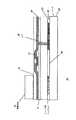
図1に、本発明の一実施形態に係る方法により形成された電子デバイス10を示す。図中の薄膜部品12は導体、TFT、ダイオード等の部品であり、フレキシブルな基板20の片面28上に形成されている。その基板28は例えばプラスチック複合素材で形成されている。その複合素材としては、一種類又は複数種類の接合用微粒子状素材及び一種類又は複数種類のバインド用プラスチック素材(プラスチックバインダ;後述)を含む素材を使用している。基板20は、その形成プロセスの大半ではキャリア例えばガラスシートに付着させておき、製品完成時にはこの図の如き状態にする。面28上に形成されている層14は、面28を絶縁化すると共に平坦化(プラナリゼーション)即ち平滑化することによって、部品12の形成に適した面にする層である。この層14は複数層設けることもできる。また、層14を例えば窒化シリコンで形成すれば、それ一層で面28を封止及び絶縁し薄膜成長に適した面にすることができる。或いは、BCB(benzocyclobutene)又はSOG(spun-on glass)からなる補助層をプラナリゼーションに用いてもよい。このようにプラナリゼーションに使用した場合、層14のことを、従来に倣いプラナリゼーション層と呼ぶことができる。 FIG. 1 shows an
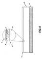
基板20の他面(符号省略)にはトレース層30が形成されている。この層30は、その面に被着又は成長させた金属被覆を、あるパターンに従ってエッチングすることによって形成したものである。必要なら、フレキシブルなプラスチック素材からなるベース層34を設けることもできる。ビア36は、層30のパターン即ちトレースパターンと共に、薄膜部品12を他の部品と接続するのに1個又は複数個使用される。図2にその断面を示す搭載部品38は、例えばシリコンその他の半導体ベース素材で形成された従来型の半導体部品である。部品38は複数個搭載することもでき、電子回路の一部を構成している。また、同図に示すように、トレースパターンの隙間を埋めるよう層30にフィラ40を入れることもできる(入れないでおくこともできる)。そして、主として絶縁及びプラナリゼーションのため、保護層44を設けることもできる。 A
図3に、他の実施形態として複数個のトレース層30及び31を有する構成を示す。それら2個の層30,31間には絶縁体42がある。層30,31のうち一方は電源又は接地との接続に使用されており、他方は薄膜部品12と他の部品との間の信号伝送に使用されている。必要ならば、EMI(電磁干渉)遮蔽用に更なるトレースパターンの層を設けることもできる。 FIG. 3 shows a configuration having a plurality of trace layers 30 and 31 as another embodiment. There is an
本発明では、更に、プラスチックバインダ中に微粒子状素材を適切に同居(co-optimization)させたものを基板の少なくとも片面に被着させる。また、適当なキャリア素材及びプロセスを用い、薄膜デバイス形成層をフレキシブル基板に接合することにより、その基板内に生じるストレスを抑える。 In the present invention, furthermore, a material in which a particulate material is appropriately co-optimized in a plastic binder is deposited on at least one side of the substrate. Further, by using an appropriate carrier material and process, the thin film device forming layer is bonded to the flexible substrate, thereby suppressing the stress generated in the substrate.
ここでいう「プラスチック」とは高重合成分を含む素材のことである。通常は、合成樹脂ポリマに他の成分、例えば硬化剤、フィラ、補強剤、着色剤、可塑剤等を入れて生成する。「樹脂」とは合成又は天然ポリマのことである。プラスチック素材を用い固体電子デバイスを形成するプロセスでは、そのプラスチック素材を流動、変形させる工程や、溶剤を適切な速度で蒸散させることでプラスチック素材を整形、硬化させる工程を実施する。使用するプラスチック素材は熱可塑性でも熱硬化性でもよい。「フレキシブル」とは、概略、そのプラスチック素材のシート厚が約1mm未満、弾性率Eが約100000〜500000psiであることをいう(1psi=約7122Pa)。 Here, “plastic” refers to a material containing a highly polymerized component. Usually, it is produced by adding other components such as a curing agent, a filler, a reinforcing agent, a coloring agent, and a plasticizer to the synthetic resin polymer. A “resin” is a synthetic or natural polymer. In the process of forming a solid electronic device using a plastic material, a step of flowing and deforming the plastic material and a step of shaping and curing the plastic material by evaporating a solvent at an appropriate speed are performed. The plastic material used may be thermoplastic or thermosetting. “Flexible” generally means that the sheet thickness of the plastic material is less than about 1 mm and the elastic modulus E is about 100,000 to 500,000 psi (1 psi = about 7122 Pa).
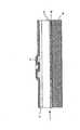
図1〜図3に示した電子デバイス10を形成するに当たっては、その基板20を特徴的な手法で構造調整する。即ち、相応のプラスチック素材で形成した基板20を微粒子状素材で表面処理し、面28又はその近傍に微粒子状素材をしみこませる。図4に、こうして複合素材化された基板20の一例構造を一部拡大して示す。この例では、基板20の下地となるプラスチック素材に微粒子状素材16が添加されており、当該下地プラスチック素材がプラスチックバインダとして働き素材16の微粒子をつなぎ止めている。素材16としては、絶縁、パッシベーション、平滑化等のための層14を基板20に接合させることができ、且つプラスチック基板20のCTEを修正することができるよう、適当な種類の固体微粒子を使用する。基板20の表面付近に素材16が添加されていると、従来は薄膜を成長させにくかったPTFE等の基板上に、TFTその他の薄膜部品12を形成することができる。即ち、基板20の表面をこのように処理することで、電子デバイスやそれに付随する接続導体(トレース)等の部品をフレキシブルな基板20上に形成することが可能になる。また、こうして複合素材化された基板20は、薄膜部品形成時の高温に耐えることや、種々の薄膜デバイス形成プロセス及びエッチング剤に耐えることができる。そして、この種の処理はフレキシブルな基板20の片面だけでなく両面にも施すことができる。両面に施すことで、薄膜部品形成に適した面だけでなく、トレースパターン形成に適した面も作り出すことができる。 In forming the
[プラスチックバインダ]
本発明の実施形態に係る方法では、プラスチック素材中に相応の微粒子状素材16を添加することで、フレキシブル基板12の素材として使用可能なプラスチック素材を次の通り多様化している。即ち、使用できるプラスチック素材は多く、HS−PET(熱安定化PET)、PEN(polyethylenenapthalate)、PC(polycarbonate)、PAR(polyarylate)、PEI(polyetherimide)、PES、PI、テフロン、PFA(poly(perfluoro-alboxy) fluoropolymer)、PEEK(poly(ether ether ketone))、PEK(poly(ether ketone))、PETFE(poly(ethylene tetrafluoroethylene)fluoropolymer)、PMMA(poly(methyl methacrylate))、各種アクリラート/メタクリラートコポリマ等も使用できる。なかでもバインダに適するプラスチック素材としては、種々の環状ポリオレフィン、JSR株式会社製のARTON(登録商標)、Zeon Chemicals L.P.製のZeonor(登録商標)、Celanese AG.製のTopas(登録商標)等がある。他種低融点プラスチック素材、例えばAusimont U.S.A.,Inc.がHALAR(登録商標)なる名称で市販しているE−CTFE(ethylene-chlorotrifluoro ethylene)、Dupont CorporationがTEFZEL(登録商標)なる名称で市販しているE−TFE(ethylene-tetra- fluoroethylene)、PTFE、FEP(ガラス繊維強化プラスチック)、HDPE等も使用できる。透明なプラスチック素材が重宝される用途もある。[Plastic binder]
In the method according to the embodiment of the present invention, the plastic material that can be used as the material of the
これらのプラスチック素材のなかには、微粒子状素材16の添加でより高温、例えば約200℃以上の最高温度での処理に耐えうるようになるものもある。なかには、300℃以上に達する高温での処理でも、損傷が生じないものもある。 Some of these plastic materials can withstand processing at higher temperatures, for example, a maximum temperature of about 200 ° C. or more, with the addition of
プラスチックバインダとして特に注目に値する素材としては、前掲のPIの他に、DuPont,Inc.がテフロンなる名称で市販しているPTFEやPFAがある。先に触れた通り、従来の手法で形成されたPIやPTFEは、様々な表面処理手法で限定的に成功を見ているとはいえ、薄膜成長用基板としての適性が十分に備わっているとはいえなかった。しかし、本発明に従い処理すれば、これらの素材によって、TFT回路形成に非常に相応しい性質を有するフレキシブル基板を実現することが可能になる。 In addition to the above-mentioned PI, DuPont, Inc. includes materials that are particularly notable as a plastic binder. There are PTFE and PFA marketed under the name Teflon. As mentioned earlier, although PI and PTFE formed by conventional methods have seen limited success with various surface treatment methods, they are sufficiently suitable as thin film growth substrates. I could not say. However, if processed according to the present invention, these materials make it possible to realize a flexible substrate having properties very suitable for TFT circuit formation.
更に、複数種類のプラスチック素材を含有する複合素材も好適に使用することができる。例えば、PIとPTFE又はPFAを併用することで、両プラスチック素材の利点をより強めることができる。 Furthermore, a composite material containing a plurality of types of plastic materials can also be suitably used. For example, by using PI in combination with PTFE or PFA, the advantages of both plastic materials can be further enhanced.
[微粒子状素材の性質]
微粒子状素材16としては、ガラス(例えばSOG)、炭素、金属、プラスチック等の繊維や、グラスファイバ織布等の織物を使用するのが望ましい。素材16が採りうるその構造的性質及び形状は多様であり、例えば略球状粒子やプレートレット(円盤状粒子)にすることができる。その寸法は基板厚より小さくても大きくてもよい。また、素材16は、ワイヤ、ロッド、繊維等の長尺体にすることもできる。セラミクスフィラその他の誘電体素材を素材16として用いることもできる。[Properties of particulate material]
As the
プラスチックバインダ中で微粒子状素材16が採りうる向きも多岐に亘っている。例えばその素材16が長尺体である場合の並び方は、一軸に沿って並ぶ、層毎に異なる軸に沿って並ぶ、平面内の複数軸に沿って並ぶ等様々である。また、基板表面に対する素材16の向き又はそのパターン次第で、その複合素材基板20の光学的、電気的、熱的、磁気的化学的乃至物理的異方性が変化する。例えば素材16として繊維状のものを用いた場合、それをバインダ内に鉛直配置することで、光や熱を鉛直方向沿いに案内可能となる。また、素材16として導光性のある繊維状のものを用いた場合、それを沿面配置することで、基板20を通る光を他方向に案内可能となる。 There are a wide variety of orientations that the
微粒子状素材16として無機素材を導入すれば、
・ 任意の光学特性、例えば色特性や散光特性の調整
・ 任意の電気特性、例えば炭素フィラによる導電性や電気遮蔽性の提供
・ 任意の熱特性、例えば金属粒子フィラによる熱伝導率の向上
・ 任意の磁気特性、例えば強磁性粒子等の磁性粒子を用いた磁気吸着性又はデータ記録能力の付与
・ 化学特性例えば薬剤処理耐性や、物理特性例えばCTE、引張強度、圧縮強度、弾性強度、可撓性等の調整
・ 輻射特性、例えば放射線遮蔽性や波長選択的X線透過性/吸収性の付与
等、様々に特性調整を施すことができる。If an inorganic material is introduced as the
-Arbitrary optical properties such as color and diffuse properties adjustment-Arbitrary electrical properties such as conductivity and electrical shielding provided by carbon filler-Arbitrary thermal properties such as metal particle filler for improved thermal conductivity-Arbitrary Of magnetic properties, for example, magnetic adsorption using magnetic particles such as ferromagnetic particles, or data recording ability-Chemical properties such as drug treatment resistance, physical properties such as CTE, tensile strength, compressive strength, elastic strength, flexibility -Various adjustments can be made to the radiation characteristics such as the provision of radiation shielding properties and wavelength-selective X-ray transmission / absorption.
重要なことに、本発明に従い微粒子状素材16をプラスチックバインダに入れることで、CTE不一致を抑えることが可能になる。これは、薄膜部品形成層・プラスチックバインダ間のCTE差に比べ、薄膜部品形成層・複合素材基板20間のCTE差を小さくすることができるためである。即ち、基板20のCTEを、従来からデバイス形成に使用されているガラス又はシリコン製のキャリア18のCTEに、より近づけることができる。その結果、薄膜部品形成層内での薄膜形成時応力発生が抑えられ、デバイスとしての性能、寸法安定性及び信頼性が向上する一方、薄膜部品12が基板20から分離する剥離が生じにくくなる。 Significantly, by placing the
ガラスやセラミクス等の微粒子状無機素材を微粒子状素材16として添加した場合は、更に
・ プラスチックバインダのみの面に比べ微粒子含有面の方が接着性がよいため、薄膜部品形成層がより強固に固着する
・ デバイス形成上限温度の向上:寸法安定性が損なわれる温度が素材16の使用で上昇するため、より高温でのデバイス形成が可能になる
・ 素材の組合せによっては、素材16の使用で基板20の比誘電率が低下し静電容量が小さくなる
といった諸効果も生じる。When a fine particle inorganic material such as glass or ceramic is added as the
そして、微粒子状素材16として透明素材を使用することは、多くの用途で有益なことである。光学的挙動が重視される場合は、素材16の屈折率n1とプラスチックバインダの屈折率n2とが所望の関係になるよう素材16を選定すればよい。例えば、屈折率n1,n2を互いに一致又は極力接近させることで光の散乱を抑えることができる。屈折率n1,n2が互いに近ければ近いほど、光の散乱は少なくなる。また、光を散乱させたい場合は、屈折率n1,n2間の差を広げること、例えば約0.1超の差にすることで、光の散乱を相応に強めることができる。更に、不透明素材や反射性素材も使用することができる。そして、プラスチックバインダに素材16に加え吸光性着色剤を添加することで、漏洩光を吸収させ、色を付け、或いは入出射光を濾波することができる。同様に、プラナリゼーション層14にも着色剤を添加できる。The use of a transparent material as the
[例1]
この例では、複合素材基板20の素材としてPTFEとガラスファイバ織布の積層体を使用する。例えば米国カリフォルニア州ランチョクーカモンガ所在のArlon,Inc.から入手できるDiClad522,527シリーズの素材である。この積層体は、温度ストレス下でもその寸法があまり変化しないため、従来からPCB用に用いられている。そうした用途では、その上に電着等で銅の層を形成するのが普通である。フレキシブル基板20として用いるのであれば、PTFEガラスファイバ織布積層体の厚みは、約25〜3000μmの範囲内にするのが望ましい。[Example 1]
In this example, a laminate of PTFE and glass fiber woven fabric is used as the material of the
この例では、その種の基板20を使用し次の手順で電子デバイス10を形成する:
1.キャリア18上への実装。本工程では、まずガラス製のキャリア18上にフレキシブル基板20を積載する。その際には、キャリア18上に基板20を配置し、それらを一体に加熱及び加圧してPTFE素材の流動化温度Tg即ち約300℃まで昇温させる。すると、基板20内のPTFE素材が軟化及び流動化(リフロー)してキャリア18の表面と結合する;
2.表面処理。本工程では、基板20の表面を処理することによって、層14を固着させるための下地を形成する。層14は例えばプラナリゼーション層であるが、その他の副次素材や薄膜電子デバイス形成素材の層でもよい。いずれにせよ、この処理によって、微粒子状素材16が基板20の表面下に埋め込まれることとなる。素材16の埋込先は、図4に示した通り、基板20の表面に近い部位が望ましい。基板表面下に素材16を埋め込む手法としては、ローリング、ダスティング等の諸手法の他、インクジェット成長、印刷、中間媒体からの転写、ドクターブレードスカイビング法による(例えば溶剤内での)被着、スプリンクリング等の被着手法も使用できる。また、素材16の埋込が進むようプラスチックバインダを加熱してもよいし、硬化処理中のプラスチックバインダに素材16を添加してもよい。使用できる他の表面処理手法については後述する;
3.プラナリゼーション。薄膜部品形成面に求められる表面粗さは、その用途にもよるが、例えばピークトゥピーク値で0.2〜0.3μm未満のオーダである。これを達成するため、本工程ではSOGを堆積させる。SOGを被着させるには、コロイダルシリカ粒子ゾル入り溶剤を基板20の表面に付着させればよい。300〜400℃の温度でそのゾル素材を硬化させると溶剤が蒸散してゲルが残留し、そのゲルが熱せられて約3〜5の比誘電率εを有するSiO2膜に変化する。薄膜成長に必要な絶縁性及び平坦度はこの膜で実現される。使用できる他のプラナリゼーション素材については後述する。In this example, an
1. Mounting on
2. surface treatment. In this step, a surface for fixing the
3. Planarization. The surface roughness required for the thin film component forming surface is, for example, on the order of 0.2 to 0.3 μm or less in peak-to-peak value, depending on the application. In order to achieve this, SOG is deposited in this step. In order to deposit the SOG, a solvent containing colloidal silica particle sol may be attached to the surface of the
本発明の実施形態に係る方法では、CTE一致度の向上と共に又はその結果として、基板20の表面に対する薄膜部品12の結合強度が高まる。これは、微粒子状素材16が複合素材基板20の表面付近から外向きにやや出っ張って層14との結合面が形成されているためである。層14を窒化シリコン、酸化シリコン等の絶縁性酸化物で形成する場合、この素材16無しではその層14を基板表面にうまく結合させ得ず、面28上に薄膜デバイス等の電子デバイスを形成して動作させることも覚束ない。 In the method according to the embodiment of the present invention, the bonding strength of the
4.電気絶縁層の形成。下処理用の基板表面処理工程のうちの最後の工程として、プラナリゼーション層14の頂面上に電気絶縁層を成長させる工程を実施することができる。本工程で成長させる電気絶縁層は、例えばSiO2、SiNx、SiON或いはその任意の組合せからなる層であり、その厚みは例えば約0.5〜1.5μmの範囲内である;
5.薄膜部品12の形成。フレキシブル基板20表面の下処理が済んだら部品12の諸構成要素の形成を開始する。本工程では、通常、基板20上に半導体薄膜層を成長させ、その半導体素材の部位選択的除去によりパターンを形成する。その際に使用するプロセスは、ゲート、ソース及びドレイン部分並びに関連する諸層の形成手法としてデバイス形成分野で周知のプロセスを使用する;
6.キャリア18からの剥離。本工程では、基板20内プラスチック素材の流動化温度Tgに迫る温度まで加熱することで、キャリア18から基板20を分離させる。分離した基板20は他の面に積載してもよいし、その熱を冷ましてもよい;
7.トレース層30のパターニングによる相互接続用トレース形成。本工程では、フォトレジストその他のマスキング法を用い従来型のエッチングプロセスを実行する。即ち、露光後にエッチング剤を被着させて未露光部から金属を除去することで、所要パターンの相互接続用トレースを形成する;
8.ビア36の形成。本工程では、従来からPCBで層間接続に使用されてきた手法を応用し、メッキによってビア36を形成する;
これらの基本工程が済んだ後に、保護層を形成する処理、電子デバイス10にコネクタ等の構造を設ける処理等を、実行することもできる。例えば、デバイス10の表裏両面に保護用のSOG被覆を形成するとよい;
また、以上の手順は、使用する基板及び形成するデバイスの種類に応じて変形することができる。例えば、誘電体層をスピンコーティングで形成する処理を代わりに実行してもよい。4). Formation of electrical insulation layer. As the last step of the substrate surface treatment step for the pretreatment, a step of growing an electrical insulating layer on the top surface of the
5). Formation of
6). Peeling from the
7). Interconnect trace formation by patterning of the
8). Formation of
After these basic steps are completed, a process for forming a protective layer, a process for providing the
Further, the above procedure can be modified according to the type of substrate to be used and the device to be formed. For example, the process of forming the dielectric layer by spin coating may be performed instead.
[例2]
次に示す例は、複合素材基板20の構造調整用に有用な諸工程を追加した例である。その基本工程は次の通りである:
1.プラスチックバインダをその融点Tgまで加熱;
2.熔融したプラスチックバインダに微粒子状素材16をフィラとして添加。接合強度を高めるには素材16を基板20の表面又はその付近に集めるべきだが、CTE差を抑えるにはプラスチックバインダ内にくまなく分散させるべきである。これを折衷するには、素材16の高濃度にするか、基板20の表面近傍に素材16を露出させればよい。そのため、本工程では、熔融させたバインダ内に素材16を十分混ぜ込む必要がある;
3.キャリア18上への実装。本工程では、こうして形成したフレキシブル基板20を、図7Aに示すようにガラス製のキャリア18上に積載する。その際には、キャリア18上に基板20を配置し、それらを一体に加熱及び加圧してプラスチックバインダ例えばPTFE素材の流動化温度Tg即ち約300℃まで昇温させる。すると、基板20内のバインダが軟化及び流動(リフロー)してキャリア18の表面と結合する;
4.プラナリゼーション。薄膜部品形成面に求められる表面粗さは、その用途にもよるが、例えばピークトゥピーク値で0.2〜0.3μm未満のオーダである。これを達成するため、本工程では、図7Bに示すように、プラナリゼーション層14となるSOGを堆積させる。SOGを堆積させるには、例えばコロイダルシリカ粒子ゾル入り溶剤を基板20の表面に付着させればよい。300〜400℃の温度でそのゾル素材を硬化させると溶剤が蒸散してゲルが残留し、そのゲルが熱せられて約3〜5の比誘電率εを有するSiO2膜に変化する。薄膜成長に必要な絶縁性及び平坦度はこの膜で実現される。使用できる他のプラナリゼーション素材については後述する;
5.電気絶縁層の形成。下処理用の基板表面処理工程のうちの最後の工程として、層14の頂面上に電気絶縁層を成長させる工程を実施することができる。本工程で成長させる電気絶縁層は、例えばSiO2、SiNx、SiON或いはその任意の組合せからなる層であり、その厚みは例えば約0.5〜1.5μmの範囲内である;
6.薄膜部品12の形成。基板20表面の下処理が済んだら部品12の諸構成要素の形成を開始する。本工程では、ゲート、ソース及びドレイン部分並びに関連する諸層の形成プロセスとしてデバイス形成分野で周知のプロセスを使用する。そのプロセスでは、半導体素材を堆積させて部位選択的に除去することでパターンを形成する。すると、図7Cに示す如き部品12が形成される;
7.保護層44の付加。図7Dに示すように、部品12を護る層44を形成することもできる;
8.キャリア18からの剥離。本工程では、基板20を形成しているプラスチック素材の流動化温度Tgに迫る温度まで加熱することでキャリア18から基板20を分離させる。分離した基板20は他の面に積載することができる。その熱を冷ますようにしてもよい。これ以外の剥離法を用いることもできる;
9.トレース層30のパターニング。本工程では、層30をエッチングすることにより、図7Eに示すように、所望のパターンとなるよう部品間接続用トレースを形成する。その際フィラ40を入れてもよい;
10.ベース層34の付加。図7Fに示すように、層30に層34を被せる工程を実施してもよい。この層34をSOGにすれば保護兼絶縁被覆となる;
11.ビア36の形成。本工程では、図7Gに示すように、層30内の相互接続用トレースに薄膜部品12を接続するため、1個又は複数個のビア36を形成する。ビア36は、在来手法による穿孔やレーザの利用で形成することができる。[Example 2]
The following example is an example in which various processes useful for adjusting the structure of the
1. Heating the plastic binder to its melting point Tg;
2.
3. Mounting on
4). Planarization. The surface roughness required for the thin film component forming surface is, for example, on the order of 0.2 to 0.3 μm or less in peak-to-peak value, depending on the application. In order to achieve this, in this step, as shown in FIG. 7B, SOG to be the
5). Formation of electrical insulation layer. As the last step of the substrate surface treatment step for the pretreatment, a step of growing an electrical insulating layer on the top surface of the
6). Formation of
7). Addition of
8). Peeling from the
9. Patterning of the
10. Addition of
11. Formation of
[例3]
この例では、PI系バインダ乃至複合素材を用いた基板形成を含む次の手順を実行する;
1.相応のキャリア18を未硬化プラスチックバインダで被覆。本工程では、硬化途中のバインダ例えばPIでキャリア18を被覆する。その未硬化PIを付着させる手法としては、ディップスカイビング、スパンオン塗布、押出等、種々の手法を用いることができる;
2.プラスチックバインダ硬化プロセスの大半を実施;
3.硬化プロセスの約80%が済んだら、フレキシブル基板20の表面に微粒子状素材16を添加。被覆厚を均等にするには、素材16を基板表面にスプリンクリングすればよい;
4.硬化プロセス完遂による残存溶剤の灼き飛ばし;
5.プラナリゼーション。薄膜部品形成面に求められる表面粗さは、その用途にもよるが、例えばピークトゥピーク値で0.2〜0.3μm未満のオーダである。これを達成するため、本工程ではSOGを堆積させる。SOGを堆積させるには、コロイダルシリカ粒子ゾル入り溶剤を基板20の表面に付着させればよい。300〜400℃の温度でそのゾル素材を硬化させると溶剤が蒸散してゲルが残留し、そのゲルが熱せられて約3〜5の比誘電率εを有するSiO2膜に変化する。薄膜成長に必要な絶縁化及びプラナリゼーションはこの膜で実現される。使用できる他のプラナリゼーション素材については後述する。必要なら、プラナリゼーション素材を金属トレースパターン上に被着させることもできる;
6.電気絶縁層の形成。下処理用の基板表面処理工程のうちの最後の工程として、プラナリゼーション層14の頂面上に電気絶縁層を成長させる工程を実施することができる。本工程で成長させる電気絶縁層は、例えばSiO2、SiNx、SiON或いはその任意の組合せからなる層であり、その厚みは例えば約0.5〜1.5μmの範囲内である;
7.薄膜部品12の形成。基板20の表面の下処理が済んだら部品12の諸構成要素の形成を開始する。本工程では、ゲート、ソース及びドレイン部分並びに関連する諸層の形成プロセスとしてデバイス形成分野で周知のプロセスを使用する。このプロセスでは、半導体素材を堆積させて部位選択的に除去することでパターンを形成する;
8.キャリア18からの剥離。本工程では、基板20内プラスチック素材の流動化温度Tgに迫る温度まで加熱することでキャリア18から基板20を分離させる。分離した基板20は他の面に積載することができる。その熱を冷ますようにしてもよい。これ以外の剥離法を用いることもできる;
9.トレース層30のパターニング。本工程では、図7Eに示すように、層30をエッチングすることにより所望パターンの部品間接続用トレースを形成する。前述の通り、その際にフィラ40を入れてもよい;
10.ベース層34の付加。図7Fに示すように、層30に層34を被せる工程を実施してもよい。この層34をSOGにすれば保護兼絶縁被覆となる;
11.ビアの形成。本工程では、図7Gに示すように、層30内の相互接続用トレースに部品12を接続するため、1個又は複数個のビア36を形成する。ビア36は、在来手法により穿孔し電解メッキ又はリベット挿入を施して形成するか、或いはレーザを利用して形成すればよい。[Example 3]
In this example, the following procedure is performed including substrate formation using a PI binder or composite material;
1. Corresponding
2. Perform most of the plastic binder curing process;
3. After about 80% of the curing process, the
4). Removing residual solvent by completing the curing process;
5). Planarization. The surface roughness required for the thin film component forming surface is, for example, on the order of 0.2 to 0.3 μm or less in peak-to-peak value, depending on the application. In order to achieve this, SOG is deposited in this step. In order to deposit SOG, a solvent containing colloidal silica particle sol may be attached to the surface of the
6). Formation of electrical insulation layer. As the last step of the substrate surface treatment step for the pretreatment, a step of growing an electrical insulating layer on the top surface of the
7). Formation of
8). Peeling from the
9. Patterning of the
10. Addition of
11. Via formation. In this step, as shown in FIG. 7G, one or
なお、未硬化プラスチックバインダに微粒子状素材16を添加するようにしてもよい。例2で説明したCTE上の利点はその手法でも享受できる。 Note that the
[PCB上での薄膜成長]
この例では、図8にその断面を示す通り、PCB46上に薄膜部品12を直接形成する。即ち、PCB46の表面上に複数個の部品12を直に形成する。通例に倣い、このPCB46は、それぞれその導電性が高い導体層を担持する絶縁基板50を複数枚、その基板50で導体層間が絶縁分離されるよう熱及び接着剤を用いて積層化した構成を採っている。また、この例では、その絶縁基板50としてFR−4を用いたPCB46上に、複数個のTFTデバイスを直接形成する。FR−4は、グラスファイバ織布のマットにエポキシ樹脂を含ませた素材である。[Thin film growth on PCB]
In this example, the
この例に係るTFT形成手順では、PCB46上に次の手順で薄膜を成長させる;
1.プラナリゼーション。本工程は、図8に示すように、所要トレースパターン層30,31等をPCB46上に形成した後に実施する。薄膜部品形成面に求められる表面粗さは、その用途にもよるが、例えばピークトゥピーク値で0.2〜0.3μm未満のオーダである。これを達成するため、本工程では、同図に示すようにプラナリゼーション層14となるSOGを基板50上に堆積させる。SOGを堆積させるには、コロイダルシリカ粒子ゾル入り溶剤を基板50の表面に付着させればよい。300〜400℃の温度でそのゾル素材を硬化させると溶剤が蒸散してゲルが残留し、そのゲルが熱せられて約3〜5の比誘電率εを有するSiO2膜に変化する。薄膜成長に必要な絶縁性及び平坦度はこの膜で実現される。なお、プラナリゼーション素材として使用できる素材は他にもある;
2.電気絶縁層の形成。下処理用に基板50の表面を処理する工程のうちの最後の工程として、層14の頂面上に電気絶縁層を成長させる工程を実施することができる。その電気絶縁層は例えばSiO2、SiNx、SiON或いはその任意の組合せからなる層であり、その厚みは例えば約0.5〜1.5μmの範囲内である;
3.薄膜部品12の形成。基板50の表面の下処理が済んだら部品12の諸構成要素の形成を開始する。本工程では、ゲート、ソース及びドレイン部分並びに関連する諸層の形成プロセスとしてデバイス形成分野で周知のプロセスを使用する。このプロセスでは、半導体素材を堆積させて部位選択的に除去することでパターンを形成する;
4.保護層44の付加。図8に示すように、部品12を護る層44を形成することもできる;
5.ビア36の形成。本工程では、図8に示すように、トレース層30内の相互接続用トレースに部品12を接続するためのビア36を1個又は複数個形成する。ビア36は在来手法による穿孔やレーザの利用で形成することができる。本工程では、ビア36としてビアホール(貫通孔)、ブラインドビア(盲孔)及びベリードビア(埋め孔)のいずれも形成することができる;
6.他の部品38の搭載。トレース層30,31との接続用のビア36が形成されたら、図8に例示するように、他の半導体部品38を部品12の周囲等に配置する。In the TFT formation procedure according to this example, a thin film is grown on the
1. Planarization. This step is performed after the required trace pattern layers 30, 31 and the like are formed on the
2. Formation of electrical insulation layer. As the last step of processing the surface of the
3. Formation of
4). Addition of
5). Formation of
6). Mounting of
なお、上掲の諸工程のうち幾つかは適宜入れ替えることができる。例えば高温加熱処理を実施する場合は、第5工程たるビア形成を第3工程たる薄膜部品形成より先に実行する方がよい。 It should be noted that some of the above-described steps can be appropriately replaced. For example, when performing a high-temperature heat treatment, it is better to execute the via formation as the fifth step before the thin film component formation as the third step.
このように、PCB46を形成する層と薄膜部品12を形成する層とを積層させることで、金属トレース又はその一部を低抵抗且つ小静電容量なPCB46内に形成することができ、また1個又は複数個の薄膜部品形成層内に半導体デバイスを形成することができる。それらの薄膜部品形成層とPCB形成層との間の電気的接続は、部品12を形成する半導体層又は金属層と、PCB46の頂面にある金属層との間の接続により行うことができる。こうした構成には
・ PCB46の金属層は大断面でありその抵抗値が低いので、より多くの電流を流すことができ、立ち上がり時間が短くなり、電力損失(I2R)が少なくなる
・ PCB46の金属層が幅広である分層間静電容量が小さくなるので、立ち上がり時間が短くなり、静電容量充放電に伴う電力損失が少なくなり、層間の容量性結合による漏話が少なくなる
・ PCB46は多数の層から形成されるので、信号伝送や電源及び接地との接続に使用できる層が多くより複雑な回路を形成できる
・ PCB46側の厚い金属層を利用できるので、従来の薄膜デバイスに比べて熱損失が少なくなる
・ 複数の電源プレーン及び接地プレーンに形成した幅広の金属層を利用できるので、大面積に亘り好適に、電源を配分することができる
・ PCB46を形成するためのプロセスは低コストであるので、金属層やビアを低コストで形成することができ、ひいては薄膜型の電子デバイス10を低コストで形成することができる
といった利点がある。Thus, by laminating the layer forming the
また、この例に係る電子デバイス10は、表示装置用バックプレーンとして形成することができる。その場合、ローアドレッシング、カラムアドレッシング、各画素へのデータ伝送、電源や接地との接続、各種タイミング信号及びクロック信号の供給等といった機能のうち一種類又は複数種類をPCB形成層で、またスイッチング機能や表示画素駆動機能は薄膜部品形成層で、それぞれ実現することができる。縦横に走るタイミング信号線、クロック信号線及びデータ信号線は例えばPCB形成層内に設ける。それらの層をPCB46の頂面にある層に接続するビア36は、例えば画素毎に或いは画素群毎に設ける。各薄膜部品12との接続は、その部品12上の金属層を介して、或いはその部品12の実装先PCB46の頂面上にある金属層を介して行う。 Further, the
この例に係る電子デバイス10は、更に、イメージセンサ用バックプレーンとしても形成することができる。その場合、ローアドレッシング、カラムアドレッシング、各画素へのデータ伝送、電源や接地との接続、各種タイミング信号及びクロック信号の供給等といった機能のうち一種類又は複数種類をPCB形成層で、またスイッチング機能やセンシング画素駆動機能は薄膜部品形成層で、それぞれ実現することができる。縦横に走るタイミング信号線、クロック信号線及び検知信号線は例えばPCB形成層内に設ける。それらの層をPCB46の頂面にある層に接続するビア36は、例えば画素毎に或いは画素群毎に設ける。各薄膜部品12との接続は、その部品12上の金属層を介して、或いはその部品12の実装先PCB46の頂面上にある金属層を介して行う。 The
PCB46の基板50は、FR−4以外にも様々な素材で形成することができる。なかでも低誘電率且つ低損失な素材としては、例えば米国コネチカット州ロジャース所在のRogers Corporationから入手可能なRogers4000及びRogersDuroid(登録商標)がある。テフロンのタイプGT及びタイプGX、PI、ポリスチレン、架橋ポリスチレン等も、基板50の形成素材として使用することができる。 The
[表面処理手法]
基板20,50に対する処理、即ち層14等の薄膜部品構成要素の固着強度を高めるための処理は、多々ある様々な手法で行うことができる。前述の通り、本発明に係る方法が最も奏功するのは微粒子状素材16の表面が基板20の表面から露出し、それによって層14との結合面が形成されているときである。しかし、基板20内でバインダとして使用されているプラスチック素材の性質上、素材16をフィラとして用いたときでも基板20の表面のうちかなりの部分をそのプラスチック素材が占めるのが普通である。そのため、素材16の存在比率ひいては層14の結合強度を高めるには、基板表面沿いから幾ばくかのプラスチック素材を取り除くため、何らかの手だてを採る必要がある。[Surface treatment method]
The processing for the
図5に、微粒子状素材16の露出度を高めたときの基板表面22の形状を示す。このような面22を形成でき処理手法としては、例えば
・ エッチング剤(例えば各種の酸)等の化学物質による除去
・ プラズマエッチング
・ コロナ放電処理
・ 加熱
・ 超臨界二酸化炭素(CO2)への露出
・ レーザアブレーション
・ 真空中熱分解
等の手法がある。FIG. 5 shows the shape of the
こうした表面処理手法の適用によるプラスチックバインダの除去は、表面処理分野での習熟者(いわゆる当業者)なら容易に行えることである。図4及び図5に例示した手法、即ち基板20の表面下又はその付近に多数集まるようフィラーたる微粒子状素材16を添加即ち埋入する手法と異なり、これらの表面処理手法は、プラスチックバインダに対するフィラー素材16の混ざり方がより均一であっても或いはあまり均一でなくても適用することができる。このように処理した素材を使用することの基本的な利点は、前掲の通りCTE一致度が高まる点にある。 The removal of the plastic binder by applying such a surface treatment technique can be easily performed by a person skilled in the surface treatment field (so-called a person skilled in the art). Unlike the techniques illustrated in FIGS. 4 and 5, that is, the technique of adding or embedding the fine
また、PTFEのリフロー性を利用し表面処理の効果を強めることもできる。即ち、PTFE又はPTFEと他の適当な物質との複合素材の表面をそのガラス転移温度Tgより少し高い温度まで昇温させ、その面上に微粒子状素材16をダスティング又はスプリンクリングした後、そのPTFE乃至複合素材を冷ますと、プラナリゼーション層14等の層を好適に成長させうる表面状態になる。素材16を堆積させた後に、上掲の諸手法を用いて表面処理を施せば、その基板20の表面はより好適な状態になる。 Further, the effect of surface treatment can be enhanced by utilizing the reflow property of PTFE. That is, after raising the surface of PTFE or a composite material of PTFE and another appropriate material to a temperature slightly higher than its glass transition temperature Tg, dusting or sprinkling the
更に、図6に示す通り、ベース基板24たる第1のプラスチック素材を準備し、その上を複合素材26で被覆するようにしてもよい。素材26としては、あるプラスチックバインダ中に一種類又は複数種類の微粒子状素材16を混入させたものを使用する。従って、この手法で形成される面上には、1個又は複数個の層を成長させることができる。例えば、図中のプラナリゼーション層14や、絶縁層や、薄膜部品10の一部を構成する電子的に活性な半導体層等を、成長させることができる。 Furthermore, as shown in FIG. 6, a first plastic material that is the
[プラナリゼーション素材]
SOG以外にプラナリゼーション素材として使用できる素材としては
・ BCB、特に可動イオンを含まない半導体グレードのもの
・ アクリル
・ TEOS(Tetraethoxysilane)
等がある。[Planarization material]
In addition to SOG, materials that can be used as planarization materials are: • BCB, especially semiconductor grade materials that do not contain mobile ions • Acrylic • TEOS (Tetraethoxysilane)
Etc.
プラスチック基板を使用する試みはこれまでもなされてきたが、本発明に係る方法では、それらに比べて薄膜部品形成層の固着強度が高まる。それは、ガラス、セラミクス等の相応な微粒子性素材16が添加されているため、プラスチックバインダ単体での場合に比べて強度に固着するからである。素材16を使用することで、寸法安定性が失われる温度限界が高まるので、より高温でのデバイス形成も可能になる。 Attempts to use a plastic substrate have been made so far, but in the method according to the present invention, the adhesion strength of the thin film component forming layer is increased as compared with them. This is because the appropriate
また、本発明に係る方法は、薄膜部品12をフレキシブル基板20上に直に形成することができ、従って積層等の中間工程が不要になる点でも有益である。特に、ウェブを利用したロールトゥロールのデバイス形成に適している。即ち、第1のロールからシート状の基板20を引き出し、前述の通り表面処理して微粒子状素材16を埋め込んだ後、更なる処理を施すか或いは第2のロールに巻き取って後日使用する、といったことが可能になる。 In addition, the method according to the present invention is advantageous in that the
微粒子状素材16として使用できる微粒子状物質の種類は多く、そうした微粒子状物質を併用乃至混合して各物質の望ましい性質を発現させることもできる。それには、電子デバイス10を形成するプロセス中の様々な段階で、例えば前掲のプラズマエッチング等のツールを使用してまた別の種類の表面処理を施すとよい。本発明に係る方法では、そうした処理をシート状基板20の片面又は両面に施すことができる。例えば、プラナリゼーション層14の被着や薄膜部品12の形成に先立ち、エンボス加工等の手法を用い基板20を表面処理してパターンを形成し、そのパターンに沿い基板20上又は層14上の部品12に例えば光学部品を付設する。例えば、レンズやレンズレットのような屈折性光学部品を1個又は複数個形成する。それらのレンズ素子は、画素入出射に使用できるよう、部品12に対し所定の位置関係を採るよう形成する。また、こうした手順を使用する場合には、プロセス上の条件やデバイスの性質に応じて諸製造工程を調整乃至変形する。例えば、部品12の形成に先立ちビア36やトレースを形成するようにする。 There are many types of particulate materials that can be used as the
こうして基板20,50上に形成した薄膜部品12は信号の入出力に使用できる。即ち、その部品12の諸構成部分から信号を出力することや、諸構成部分に信号を取り込むことができるので、例えば画像表示装置やイメージセンサの画素と組み合わせることができる。例えば、基板20の表面上に形成した部品12を対応する液晶画素、発光ダイオード画素又は有機発光ダイオード画素と結合させて表示に使用することや、誘導性蛍光体画素等のセンサ画素(生体検知器等の画素)と結合させてイメージセンシングに使用することができる。 The
更に、本発明で形成するビア36には、基板上の薄膜部品12がその動作中に発生させる熱を逃がす役割もある。ビア利用放熱については、本願出願人を譲受人とする特許文献6(発明者:Switzer et al.)に、より詳細な説明がある。 Furthermore, the via 36 formed in the present invention also serves to release heat generated by the
また、基板20の片面上に形成した金属被覆パターンは、電子回路を形成する信号伝送路として用いることも、接地プレーン或いはEMIシールドとして用いることもできる。 In addition, the metal coating pattern formed on one surface of the
更に、本発明を多層基板に適用することもできる。その場合、一番下の層にはキャリアがらみの特性(対キャリア接着性等)を付与し、一番上の層には電子デバイスがらみの特性(対薄膜部品形成層接着性等)を付与し、そしてその中間にある層には指定された特性(光学特性、電気特性、熱特性、磁気特性乃至化学特性)を付与するようにするとよい。 Furthermore, the present invention can be applied to a multilayer substrate. In that case, the lower layer is given carrier characteristics (adhesiveness to carrier, etc.), and the uppermost layer is given electronic devices characteristics (adhesion to thin film component forming layer, etc.). In addition, it is preferable to give specified characteristics (optical characteristics, electrical characteristics, thermal characteristics, magnetic characteristics or chemical characteristics) to the intermediate layer.
このように、本発明によれば、基板上に電子でバイス及び相互接続用トレースを形成するための装置及び方法を得ることができる。 Thus, according to the present invention, an apparatus and method for forming vise and interconnect traces electronically on a substrate can be obtained.
10 電子デバイス、12 薄膜部品、14 プラナリゼーション層、16 微粒子状素材、18 キャリア、20 基板、22,28 基板表面、24 ベース基板、26 複合素材、30,31 トレース層、34 ベース層、36 ビア、38 搭載部品、40 フィラ、42 絶縁体、44 保護層、46 印刷回路基板、50 絶縁基板。 DESCRIPTION OF
Claims (57)
Translated fromJapaneseb)その金属被覆の一部をエッチングして金属被覆パターンを形成するステップと、
c)基板の他面に微粒子状素材を埋め込むステップと、
d)その微粒子状素材埋込面上に薄膜電子デバイスを形成するステップと、
を有する電子デバイス形成方法。a) preparing a substrate comprising one or more plastic materials and having a metal coating on one side thereof;
b) etching a portion of the metal coating to form a metal coating pattern;
c) embedding particulate material on the other surface of the substrate;
d) forming a thin film electronic device on the particulate material embedded surface;
An electronic device forming method comprising:
b)金属被覆面から見て裏側にある未被覆面に微粒子状素材を埋め込むステップと、
c)その金属被覆に対するエッチングによりトレースパターンを形成するステップと、
d)基板の微粒子状素材埋込面にプラナリゼーション素材を被着させることによりプラナリゼーション層を形成するステップと、
e)その面上に更に薄膜電子デバイスを形成するステップと、
f)その薄膜電子デバイスとトレースパターンの一部を接続するビアを形成するステップと、
を有する電子デバイス形成方法。a) preparing a substrate comprising one or more plastic materials and having a metal coating on one side thereof;
b) embedding a particulate material in the uncoated surface on the back side as viewed from the metal coated surface;
c) forming a trace pattern by etching the metal coating;
d) forming a planarization layer by depositing a planarization material on the particulate material embedding surface of the substrate;
e) forming further thin film electronic devices on the surface;
f) forming a via connecting the thin film electronic device and a portion of the trace pattern;
An electronic device forming method comprising:
b)その金属被覆内に導電性のトレースパターンを形成するステップと、
c)一種類又は複数種類のバインド用プラスチック素材と一種類又は複数種類の微粒子状素材とを含む複合素材でベース基板の他面を被覆することにより複合素材被覆面を1個又は複数個形成するステップと、
d)少なくとも1個の複合素材被覆面上に薄膜電子デバイスを形成するステップと、
を有する電子デバイス形成方法。a) preparing a substrate including one or a plurality of plastic materials to be a base substrate and having a metal coating on one surface thereof;
b) forming a conductive trace pattern in the metallization;
c) One or a plurality of composite material-coated surfaces are formed by coating the other surface of the base substrate with a composite material including one or more kinds of binding plastic materials and one or more types of particulate materials. Steps,
d) forming a thin film electronic device on at least one composite coated surface;
An electronic device forming method comprising:
b)その金属被覆パターン不具備面を処理することでその面における対プラスチック素材微粒子状素材比率を高めるステップと、
c)その処理が済んだ面上に薄膜電子デバイスを形成するステップと、
d)その薄膜電子デバイスと金属被覆パターンを接続するステップと、
を有する電子デバイス形成方法。a) preparing a substrate containing one or more types of plastic material and one or more types of particulate material, one side of which has a metal coating pattern and the other side has no metal coating pattern;
b) increasing the ratio of the particulate material to plastic material on the surface by treating the surface without the metal coating pattern;
c) forming a thin film electronic device on the treated surface;
d) connecting the thin film electronic device and the metallization pattern;
An electronic device forming method comprising:
b)その基板の片面又は両面上に薄膜電子デバイスを形成するステップと、
c)その基板の他面上に電子回路用のトレースパターンを形成するステップと、
d)そのトレースパターンと薄膜電子デバイスを接続するビアを形成するステップと、
を有する電子デバイス形成方法。a) preparing a substrate containing PTFE (polytetrafluoroethylene) and one or more kinds of particulate materials;
b) forming a thin film electronic device on one or both sides of the substrate;
c) forming a trace pattern for an electronic circuit on the other surface of the substrate;
d) forming a via connecting the trace pattern and the thin film electronic device;
An electronic device forming method comprising:
b)その基板の片面又は両面上に薄膜電子デバイスを形成するステップと、
c)その基板の他面上に金属パターン層を形成するステップと、
d)その金属パターン層と薄膜電子デバイスを接続するビアを形成するステップと、
を有する電子デバイス形成方法。a) preparing a substrate containing PTFE (polytetrafluoroethylene), one or more types of other plastic materials and one or more types of particulate materials;
b) forming a thin film electronic device on one or both sides of the substrate;
c) forming a metal pattern layer on the other surface of the substrate;
d) forming a via connecting the metal pattern layer and the thin film electronic device;
An electronic device forming method comprising:
b)その基板の片面上に金属パターン層を形成するステップと、
c)その基板をキャリアに積載するステップと、
d)その基板上に電子デバイスを形成するステップと、
e)その電子デバイスと金属パターン層を接続するビアを形成するステップと、
を有する電子デバイス形成方法。a) preparing a substrate containing PTFE (polytetrafluoroethylene) and one or more kinds of particulate materials;
b) forming a metal pattern layer on one side of the substrate;
c) loading the substrate onto a carrier;
d) forming an electronic device on the substrate;
e) forming a via connecting the electronic device and the metal pattern layer;
An electronic device forming method comprising:
b)少なくとも1枚の基板をキャリアに積載するステップと、
c)金属被覆パターンと基板の他面を結ぶビアを形成するステップと、
d)当該他面上に電子デバイスを形成するステップと、
を有する電子デバイス形成方法。a) preparing one or more substrates including a plurality of types of plastic materials and one or more types of particulate materials and having a metal coating pattern on one side thereof;
b) loading at least one substrate on a carrier;
c) forming a via connecting the metallization pattern and the other surface of the substrate;
d) forming an electronic device on the other side;
An electronic device forming method comprising:
b)その基板の片面上に金属トレースパターン層を形成するステップと、
c)その基板をキャリア層上に実装するステップと、
d)半導体薄膜成長に備えその基板の裏面を処理するステップと、
e)その処理が済んだ面上に薄膜半導体素材の層を成長させるステップと、
f)その層の半導体素材を部位選択的に除去してパターンを形成するステップと、
を有する電子デバイス形成方法。a) preparing a substrate comprising a plastic material and one or more types of particulate material;
b) forming a metal trace pattern layer on one side of the substrate;
c) mounting the substrate on the carrier layer;
d) treating the backside of the substrate in preparation for semiconductor thin film growth;
e) growing a layer of thin film semiconductor material on the treated surface;
f) forming a pattern by selectively removing the semiconductor material of the layer;
An electronic device forming method comprising:
g)加熱によりキャリア層から基板を取り外すステップを有する電子デバイス形成方法。The method of forming an electronic device according to claim 24, further comprising:
g) A method for forming an electronic device comprising the step of removing the substrate from the carrier layer by heating.
b)その基板の少なくとも片面上にパターンを形成するステップと、
c)その面に微粒子状素材を埋め込むステップと、
d)その微粒子状素材埋込面にプラナリゼーション素材を被着させることでプラナリゼーション層を形成するステップと、
e)その面上に更に薄膜電子デバイスを形成するステップと、
f)その微粒子状素材埋込面から見て裏側の面上にトレースパターン層を形成するステップと、
を有する電子デバイス形成方法。a) preparing a substrate including one or more plastic materials;
b) forming a pattern on at least one side of the substrate;
c) embedding particulate material on the surface;
d) forming a planarization layer by depositing a planarization material on the particulate material embedding surface;
e) forming further thin film electronic devices on the surface;
f) forming a trace pattern layer on the back surface as seen from the particulate material embedding surface;
An electronic device forming method comprising:
b)その金属被覆の少なくとも一部をエッチングして金属被覆パターンを形成するステップと、
c)その片面上に金属被覆パターンが形成されている第2の基板を第1の基板に取り付けるステップと、
d)第1の基板の金属被覆パターン不具備面と第1、第2又はその双方の基板上の金属被覆パターンとを結ぶビアを1個又は複数個形成するステップと、
e)第1の基板の金属被覆パターン不具備面上に薄膜電子デバイスを形成するステップと、
を有する電子デバイス形成方法。a) preparing a first substrate that includes one or more plastic materials and one side of which is coated with metal;
b) etching at least a portion of the metal coating to form a metal coating pattern;
c) attaching a second substrate having a metal coating pattern formed on one side thereof to the first substrate;
d) forming one or a plurality of vias connecting the surface of the first substrate having no metallization pattern and the metallization pattern on the first, second or both substrates;
e) forming a thin film electronic device on the surface of the first substrate having no metallization pattern;
An electronic device forming method comprising:
b)その金属被覆をエッチングすることでトレースパターンを形成するステップと、
c)基板の他面にプラナリゼーション素材を被着させることでプラナリゼーション層を形成するステップと、
d)基板のプラナリゼーション層形成面上に薄膜電子デバイスを形成するステップと、
e)その薄膜電子デバイスとトレースパターンの一部を接続するビアを形成するステップと、
を有する電子デバイス形成方法。a) preparing a substrate comprising one or more plastic materials and having a metal coating on one side thereof;
b) forming a trace pattern by etching the metal coating;
c) forming a planarization layer by depositing a planarization material on the other side of the substrate;
d) forming a thin film electronic device on the planarization layer forming surface of the substrate;
e) forming a via connecting the thin film electronic device and a portion of the trace pattern;
An electronic device forming method comprising:
b)そのうち何枚かの基板上に金属層を形成するステップと、
c)そのうち何個かの金属層をパターニングするステップと、
d)準備した複数枚の基板を互いに接合するステップと、
e)パターニングが済んだ金属層間を結ぶビアを形成するステップと、
f)基板のうち少なくとも1枚の上に電子デバイスを形成するステップと、
を有する電子デバイス形成方法。a) preparing a plurality of substrates;
b) forming a metal layer on some of the substrates;
c) patterning some of the metal layers,
d) bonding the prepared plurality of substrates to each other;
e) forming vias connecting the patterned metal layers;
f) forming an electronic device on at least one of the substrates;
An electronic device forming method comprising:
g)電子デバイス形成後に基板をキャリアから取り外すステップを有する電子デバイス形成方法。An electronic device forming method according to claim 49,
g) A method for forming an electronic device, comprising the step of removing the substrate from the carrier after forming the electronic device.
b)基板のうち1枚についてその金属層をパターニングするステップと、
c)その基板を他の基板に接合するステップと、
d)当該他の基板の金属層をパターニングするステップと、
e)パターニングが済んだ金属層間を結ぶビアを形成するステップと、
f)プラスチック基板のうち少なくとも1枚の上に電子デバイスを形成するステップと、
を有する電子デバイス形成方法。a) preparing a plurality of plastic substrates, some of which have a metal layer;
b) patterning the metal layer of one of the substrates;
c) bonding the substrate to another substrate;
d) patterning the metal layer of the other substrate;
e) forming vias connecting the patterned metal layers;
f) forming an electronic device on at least one of the plastic substrates;
An electronic device forming method comprising:
Applications Claiming Priority (2)
| Application Number | Priority Date | Filing Date | Title |
|---|---|---|---|
| US11/538,173US7977170B2 (en) | 2006-10-03 | 2006-10-03 | Flexible substrate with electronic devices and traces |
| PCT/US2007/020144WO2008042110A2 (en) | 2006-10-03 | 2007-09-18 | Flexible substrate with electronic devices and traces |
Publications (2)
| Publication Number | Publication Date |
|---|---|
| JP2010506400Atrue JP2010506400A (en) | 2010-02-25 |
| JP2010506400A5 JP2010506400A5 (en) | 2010-11-11 |
Family
ID=39268951
Family Applications (1)
| Application Number | Title | Priority Date | Filing Date |
|---|---|---|---|
| JP2009531384APendingJP2010506400A (en) | 2006-10-03 | 2007-09-18 | Flexible substrate with electronic device and trace |
Country Status (5)
| Country | Link |
|---|---|
| US (3) | US7977170B2 (en) |
| EP (1) | EP2070124A2 (en) |
| JP (1) | JP2010506400A (en) |
| TW (1) | TW200832504A (en) |
| WO (1) | WO2008042110A2 (en) |
Cited By (4)
| Publication number | Priority date | Publication date | Assignee | Title |
|---|---|---|---|---|
| JP2013168176A (en)* | 2013-05-01 | 2013-08-29 | Dainippon Printing Co Ltd | Touch panel sensor, laminated body for preparing touch panel sensor and method for manufacturing touch panel sensor |
| US8653523B2 (en) | 2010-12-01 | 2014-02-18 | Seiko Epson Corporation | Thin-film transistor forming substrate, semiconductor device, and electric apparatus |
| US8848388B2 (en) | 2011-03-02 | 2014-09-30 | Seiko Epson Corporation | Electrical device |
| JP2019121734A (en)* | 2018-01-10 | 2019-07-22 | 株式会社Joled | Semiconductor device and display device |
Families Citing this family (53)
| Publication number | Priority date | Publication date | Assignee | Title |
|---|---|---|---|---|
| KR101257851B1 (en)* | 2007-03-13 | 2013-04-24 | 삼성전자주식회사 | Thin film transistor for display and Manufacturing method for the Same |
| US9330589B2 (en) | 2011-11-16 | 2016-05-03 | Nanolumens Acquisition, Inc. | Systems for facilitating virtual presence |
| US9071809B2 (en) | 2008-01-04 | 2015-06-30 | Nanolumens Acquisition, Inc. | Mobile, personsize display system and method of use |
| US9013367B2 (en) | 2008-01-04 | 2015-04-21 | Nanolumens Acquisition Inc. | Flexible display |
| US9655267B2 (en) | 2008-01-04 | 2017-05-16 | Nanolumens Acquisition, Inc. | Retractable display system and method of use |
| US8502259B2 (en) | 2008-01-11 | 2013-08-06 | Industrial Technology Research Institute | Light emitting device |
| US8800138B2 (en)* | 2008-02-08 | 2014-08-12 | Carestream Health, Inc. | Method for conditioning a substrate surface for forming an electronic device thereon and resultant device |
| US8343822B2 (en)* | 2008-08-04 | 2013-01-01 | Panasonic Corporation | Flexible semiconductor device and method for manufacturing same |
| TWI393928B (en)* | 2008-11-19 | 2013-04-21 | Ind Tech Res Inst | Optical waveguide and manufacturing method thereof |
| US9601530B2 (en) | 2008-12-02 | 2017-03-21 | Arizona Board Of Regents, A Body Corporated Of The State Of Arizona, Acting For And On Behalf Of Arizona State University | Dual active layer semiconductor device and method of manufacturing the same |
| US9991311B2 (en) | 2008-12-02 | 2018-06-05 | Arizona Board Of Regents On Behalf Of Arizona State University | Dual active layer semiconductor device and method of manufacturing the same |
| US9721825B2 (en) | 2008-12-02 | 2017-08-01 | Arizona Board Of Regents, A Body Corporate Of The State Of Arizona, Acting For And On Behalf Of Arizona State University | Method of providing a flexible semiconductor device and flexible semiconductor device thereof |
| US8074349B2 (en)* | 2009-04-16 | 2011-12-13 | Carestream Health, Inc. | Magnetic hold-down for foil substrate processing |
| JP2011009704A (en)* | 2009-05-26 | 2011-01-13 | Seiko Epson Corp | Thin film device, flexible circuit board including thin film device, and method for manufacturing thin film device |
| KR101362025B1 (en) | 2009-05-29 | 2014-02-13 | 아리조나 보드 오브 리젠츠 퍼 앤 온 비하프 오브 아리조나 스테이트 유니버시티 | Method of providing a flexible semiconductor device at high temperatures and flexible semiconductor device thereof |
| TWI387138B (en)* | 2009-07-10 | 2013-02-21 | Ind Tech Res Inst | Magnetic light eitting device, magnetic light eitting apparatus and semi-conductive nitride template |
| KR101084230B1 (en)* | 2009-11-16 | 2011-11-16 | 삼성모바일디스플레이주식회사 | Organic light emitting display device and manufacturing method of organic light emitting display device |
| WO2011107189A2 (en)* | 2010-02-03 | 2011-09-09 | Johnson Controls Automotive Electronics Gmbh | Display device |
| WO2012021196A2 (en) | 2010-05-21 | 2012-02-16 | Arizona Board Of Regents, For And On Behalf Of Arizona State University | Method for manufacturing electronic devices and electronic devices thereof |
| WO2012021197A2 (en)* | 2010-05-21 | 2012-02-16 | Arizona Board Of Regents, For And On Behalf Of Arizona State University | Method of manufacturing electronic devices on both sides of a carrier substrate and electronic devices thereof |
| US8896015B2 (en)* | 2010-06-25 | 2014-11-25 | Axlen, Inc. | LED package and method of making the same |
| DE102010051959A1 (en)* | 2010-11-19 | 2012-05-24 | Osram Opto Semiconductors Gmbh | Optoelectronic semiconductor component |
| US8963895B2 (en) | 2011-09-22 | 2015-02-24 | Nano Lumens Acquisition Inc. | Ubiquitously mountable image display system |
| US10261370B2 (en) | 2011-10-05 | 2019-04-16 | Apple Inc. | Displays with minimized border regions having an apertured TFT layer for signal conductors |
| US9286826B2 (en) | 2011-10-28 | 2016-03-15 | Apple Inc. | Display with vias for concealed printed circuit and component attachment |
| US8937285B2 (en) | 2012-06-18 | 2015-01-20 | General Electric Company | Methods and systems for signal communication in gamma ray detectors |
| US9226347B2 (en) | 2012-06-25 | 2015-12-29 | Apple Inc. | Displays with vias |
| US9214507B2 (en) | 2012-08-17 | 2015-12-15 | Apple Inc. | Narrow border organic light-emitting diode display |
| US9454025B2 (en) | 2012-08-31 | 2016-09-27 | Apple Inc. | Displays with reduced driver circuit ledges |
| US9477354B2 (en) | 2012-11-16 | 2016-10-25 | 3M Innovative Properties Company | Conductive trace hiding materials, articles, and methods |
| KR102107456B1 (en)* | 2013-12-10 | 2020-05-08 | 삼성디스플레이 주식회사 | Flexible display device and method for manufacturing the same |
| US10381224B2 (en) | 2014-01-23 | 2019-08-13 | Arizona Board Of Regents On Behalf Of Arizona State University | Method of providing an electronic device and electronic device thereof |
| WO2015156891A2 (en) | 2014-01-23 | 2015-10-15 | Arizona Board Of Regents, Acting For And On Behalf Of Arizona State University | Method of providing a flexible semiconductor device and flexible semiconductor device thereof |
| WO2017034644A2 (en) | 2015-06-09 | 2017-03-02 | ARIZONA BOARD OF REGENTS a body corporate for THE STATE OF ARIZONA for and on behalf of ARIZONA STATE UNIVERSITY | Method of providing an electronic device and electronic device thereof |
| JP2017518638A (en) | 2014-05-13 | 2017-07-06 | アリゾナ・ボード・オブ・リージェンツ・フォー・アンド・オン・ビハーフ・オブ・アリゾナ・ステイト・ユニバーシティArizona Board Of Regents For And On Behalf Of Arizona State University | Method for providing an electronic device and the electronic device |
| US10446582B2 (en) | 2014-12-22 | 2019-10-15 | Arizona Board Of Regents On Behalf Of Arizona State University | Method of providing an imaging system and imaging system thereof |
| US9741742B2 (en) | 2014-12-22 | 2017-08-22 | Arizona Board Of Regents, A Body Corporate Of The State Of Arizona, Acting For And On Behalf Of Arizona State University | Deformable electronic device and methods of providing and using deformable electronic device |
| US9279573B1 (en) | 2015-02-09 | 2016-03-08 | Nanolumens Acquisition, Inc. | Front serviceable mounting apparatus and methods |
| US9326620B1 (en) | 2015-03-12 | 2016-05-03 | Nanolumens Acquisition, Inc. | Modular display system and methods |
| US10170711B2 (en) | 2015-05-05 | 2019-01-01 | Apple Inc. | Display with vias to access driver circuitry |
| US9830885B2 (en) | 2015-10-26 | 2017-11-28 | Nanolumens Acquisition, Inc. | Modular flexible display system and methods |
| US9924604B2 (en) | 2015-11-04 | 2018-03-20 | Nanolumens Acquisition, Inc. | Modular flexible convex display system and methods |
| US10217440B2 (en) | 2016-03-17 | 2019-02-26 | Nanolumens Acquisition, Inc. | In-situ display monitoring and calibration system and methods |
| US10667709B2 (en) | 2016-05-27 | 2020-06-02 | Board Of Trustees Of Michigan State University | Hybrid diamond-polymer thin film sensors and fabrication method |
| CN106773384A (en)* | 2016-12-20 | 2017-05-31 | 深圳市华星光电技术有限公司 | Goa circuit structure |
| TWI649440B (en)* | 2017-09-20 | 2019-02-01 | 永恒光實業股份有限公司 | Flexible substrate structure and manufacturing method thereof |
| US10892256B2 (en) | 2018-01-31 | 2021-01-12 | Nanolumens Acquisition, Inc. | Light emitting display system having improved fire performance |
| US11217566B2 (en) | 2018-12-19 | 2022-01-04 | Nanolumens Acquisition, Inc. | Light emitting display with improved wide angle color viewing |
| USD950110S1 (en) | 2019-05-29 | 2022-04-26 | Nanolumens Acquisition, Inc. | Light emitting display module with diffusely reflective facade |
| US11631703B2 (en)* | 2020-06-18 | 2023-04-18 | Barco Nv | System and method for display panel |
| US20220136141A1 (en)* | 2020-11-04 | 2022-05-05 | Elena Dimova Barakova Cowan | Fabric for garments and items providing electromagnetic radiation protection |
| US11737216B2 (en) | 2021-01-22 | 2023-08-22 | Xerox Corporation | Metal drop ejecting three-dimensional (3D) object printer |
| CN114823716B (en)* | 2021-01-29 | 2024-08-13 | 京东方科技集团股份有限公司 | A driving backplane, a display panel and a display device |
Citations (4)
| Publication number | Priority date | Publication date | Assignee | Title |
|---|---|---|---|---|
| JP2004515081A (en)* | 2000-11-30 | 2004-05-20 | インフィネオン テクノロジーズ アクチェンゲゼルシャフト | Substrate having semiconductor layer, electronic device, electronic circuit, printable composition and method of making |
| US20050163968A1 (en)* | 2004-01-20 | 2005-07-28 | Hanket Gregory M. | Microfiller-reinforced polymer film |
| JP2005311331A (en)* | 2004-03-26 | 2005-11-04 | Semiconductor Energy Lab Co Ltd | Semiconductor device |
| JP2009545878A (en)* | 2006-07-31 | 2009-12-24 | イーストマン コダック カンパニー | Flexible substrate on which electronic devices are formed |
Family Cites Families (19)
| Publication number | Priority date | Publication date | Assignee | Title |
|---|---|---|---|---|
| US2114169A (en) | 1933-10-07 | 1938-04-12 | Briggs Mfg Co | Refrigerator cabinet |
| WO1993018428A2 (en)* | 1992-03-13 | 1993-09-16 | Kopin Corporation | Head-mounted display system |
| US5817550A (en) | 1996-03-05 | 1998-10-06 | Regents Of The University Of California | Method for formation of thin film transistors on plastic substrates |
| AU1901299A (en)* | 1997-11-06 | 1999-05-31 | Lockheed Martin Corporation | Modular and multifunctional structure |
| US6451191B1 (en)* | 1999-11-18 | 2002-09-17 | 3M Innovative Properties Company | Film based addressable programmable electronic matrix articles and methods of manufacturing and using the same |
| US6418267B1 (en)* | 2000-01-13 | 2002-07-09 | Mediapull, Inc. | Micro-display driven tiled electro-optic display apparatus |
| US6492026B1 (en) | 2000-04-20 | 2002-12-10 | Battelle Memorial Institute | Smoothing and barrier layers on high Tg substrates |
| US6762124B2 (en) | 2001-02-14 | 2004-07-13 | Avery Dennison Corporation | Method for patterning a multilayered conductor/substrate structure |
| SG115456A1 (en)* | 2002-03-04 | 2005-10-28 | Micron Technology Inc | Semiconductor die packages with recessed interconnecting structures and methods for assembling the same |
| US6943056B2 (en)* | 2002-04-16 | 2005-09-13 | Renesas Technology Corp. | Semiconductor device manufacturing method and electronic equipment using same |
| JP4808966B2 (en)* | 2002-09-19 | 2011-11-02 | シャープ株式会社 | Resistance change function body and memory and electronic device including the same |
| JP2004191734A (en)* | 2002-12-12 | 2004-07-08 | Sharp Corp | Plastic substrate and liquid crystal display device having the same |
| TWI330269B (en) | 2002-12-27 | 2010-09-11 | Semiconductor Energy Lab | Separating method |
| US20060214169A1 (en) | 2003-08-11 | 2006-09-28 | Virtualblue, Llc | Active Matrix Display Backplane |
| US6812949B1 (en) | 2003-08-14 | 2004-11-02 | Eastman Kodak Company | Imaging apparatus and method for exposing a photosensitive material |
| JP2005140980A (en)* | 2003-11-06 | 2005-06-02 | Nitto Denko Corp | Laminated film |
| US7333257B2 (en)* | 2003-11-19 | 2008-02-19 | University Of Florida Research Foundation, Inc. | Device for contacting patterned electrodes on porous substrates |
| JP2005153273A (en)* | 2003-11-25 | 2005-06-16 | Nitto Denko Corp | Resin sheet, liquid crystal cell substrate, liquid crystal display device, substrate for electroluminescence display device, substrate for electroluminescence display, and substrate for solar cell |
| US7791700B2 (en)* | 2005-09-16 | 2010-09-07 | Kent Displays Incorporated | Liquid crystal display on a printed circuit board |
- 2006
- 2006-10-03USUS11/538,173patent/US7977170B2/ennot_activeExpired - Fee Related
- 2007
- 2007-09-18WOPCT/US2007/020144patent/WO2008042110A2/enactiveApplication Filing
- 2007-09-18EPEP07838365Apatent/EP2070124A2/ennot_activeWithdrawn
- 2007-09-18JPJP2009531384Apatent/JP2010506400A/enactivePending
- 2007-10-02TWTW096136915Apatent/TW200832504A/enunknown
- 2011
- 2011-05-12USUS13/106,203patent/US8288214B2/ennot_activeExpired - Fee Related
- 2011-05-12USUS13/106,197patent/US20110220610A1/ennot_activeAbandoned
Patent Citations (4)
| Publication number | Priority date | Publication date | Assignee | Title |
|---|---|---|---|---|
| JP2004515081A (en)* | 2000-11-30 | 2004-05-20 | インフィネオン テクノロジーズ アクチェンゲゼルシャフト | Substrate having semiconductor layer, electronic device, electronic circuit, printable composition and method of making |
| US20050163968A1 (en)* | 2004-01-20 | 2005-07-28 | Hanket Gregory M. | Microfiller-reinforced polymer film |
| JP2005311331A (en)* | 2004-03-26 | 2005-11-04 | Semiconductor Energy Lab Co Ltd | Semiconductor device |
| JP2009545878A (en)* | 2006-07-31 | 2009-12-24 | イーストマン コダック カンパニー | Flexible substrate on which electronic devices are formed |
Cited By (8)
| Publication number | Priority date | Publication date | Assignee | Title |
|---|---|---|---|---|
| US8653523B2 (en) | 2010-12-01 | 2014-02-18 | Seiko Epson Corporation | Thin-film transistor forming substrate, semiconductor device, and electric apparatus |
| US8848388B2 (en) | 2011-03-02 | 2014-09-30 | Seiko Epson Corporation | Electrical device |
| US9288895B2 (en) | 2011-03-02 | 2016-03-15 | Seiko Epson Corporation | Electrical device |
| US9288896B2 (en) | 2011-03-02 | 2016-03-15 | Seiko Epson Corporation | Electrical device |
| US9332634B2 (en) | 2011-03-02 | 2016-05-03 | Seiko Epson Corporation | Electrical device |
| JP2013168176A (en)* | 2013-05-01 | 2013-08-29 | Dainippon Printing Co Ltd | Touch panel sensor, laminated body for preparing touch panel sensor and method for manufacturing touch panel sensor |
| JP2019121734A (en)* | 2018-01-10 | 2019-07-22 | 株式会社Joled | Semiconductor device and display device |
| US10825882B2 (en) | 2018-01-10 | 2020-11-03 | Joled Inc. | Semiconductor device and display unit |
Also Published As
| Publication number | Publication date |
|---|---|
| US20110220610A1 (en) | 2011-09-15 |
| US20080090338A1 (en) | 2008-04-17 |
| US8288214B2 (en) | 2012-10-16 |
| US20110212555A1 (en) | 2011-09-01 |
| EP2070124A2 (en) | 2009-06-17 |
| TW200832504A (en) | 2008-08-01 |
| WO2008042110A2 (en) | 2008-04-10 |
| WO2008042110A3 (en) | 2008-07-31 |
| US7977170B2 (en) | 2011-07-12 |
Similar Documents
| Publication | Publication Date | Title |
|---|---|---|
| JP2010506400A (en) | Flexible substrate with electronic device and trace | |
| US7964507B2 (en) | Flexible substrate with electronic devices formed thereon | |
| US5925206A (en) | Practical method to make blind vias in circuit boards and other substrates | |
| JP6996976B2 (en) | High speed interconnect for printed circuit boards | |
| US9417415B2 (en) | Interposer with polymer-filled or polymer-lined optical through-vias in thin glass substrate | |
| TWI495416B (en) | Multilayered substrate | |
| US10932373B2 (en) | Circuit board, electronic circuit device, and production method of circuit board | |
| JP5406389B2 (en) | Component built-in substrate and manufacturing method thereof | |
| CN105808005A (en) | Flexible display screen and manufacturing method thereof | |
| JP2007517248A5 (en) | ||
| KR102078009B1 (en) | Printed circuit board and manufacturing method of the same | |
| KR20200070773A (en) | The method for manufacturing the printed circuit board | |
| US20140119703A1 (en) | Printed Circuit Board Comprising Both Conductive Metal and Optical Elements | |
| US9627420B2 (en) | Method for forming an electronic device on a flexible substrate supported by a detachable carrier | |
| JP2004302345A (en) | Opto-electric printed wiring board and its manufacturing method | |
| CN101778534A (en) | Photoelectric hybrid circuit board and manufacturing method thereof | |
| KR102187498B1 (en) | Method of fabricating electronic device | |
| US20150136446A1 (en) | Printed circuit board | |
| JP2022519075A (en) | Circuit board | |
| TW202005076A (en) | Systems and methods for combination high temperature and low temperature device formation | |
| KR20200009318A (en) | Method of fabricating a flexible devices | |
| EP4564420A1 (en) | Packaging substrate and manufacturing method of packaging substrate | |
| DE202023105697U1 (en) | Component carrier with electrically insulating cover structure that selectively covers an optical fiber | |
| JP2004302347A (en) | Opto-electric printed wiring board and its manufacturing method | |
| DE202022102683U1 (en) | Component carrier with at least two components |
Legal Events
| Date | Code | Title | Description |
|---|---|---|---|
| A521 | Request for written amendment filed | Free format text:JAPANESE INTERMEDIATE CODE: A523 Effective date:20100917 | |
| A621 | Written request for application examination | Free format text:JAPANESE INTERMEDIATE CODE: A621 Effective date:20100917 | |
| A521 | Request for written amendment filed | Free format text:JAPANESE INTERMEDIATE CODE: A523 Effective date:20110913 | |
| A131 | Notification of reasons for refusal | Free format text:JAPANESE INTERMEDIATE CODE: A131 Effective date:20130305 | |
| A02 | Decision of refusal | Free format text:JAPANESE INTERMEDIATE CODE: A02 Effective date:20130730 |