JP2010267341A - Semiconductor device - Google Patents
Semiconductor deviceDownload PDFInfo
- Publication number
- JP2010267341A JP2010267341AJP2009119016AJP2009119016AJP2010267341AJP 2010267341 AJP2010267341 AJP 2010267341AJP 2009119016 AJP2009119016 AJP 2009119016AJP 2009119016 AJP2009119016 AJP 2009119016AJP 2010267341 AJP2010267341 AJP 2010267341A
- Authority
- JP
- Japan
- Prior art keywords
- erase
- gate
- memory
- memory cell
- read
- Prior art date
- Legal status (The legal status is an assumption and is not a legal conclusion. Google has not performed a legal analysis and makes no representation as to the accuracy of the status listed.)
- Pending
Links
Images


Classifications
- G—PHYSICS
- G11—INFORMATION STORAGE
- G11C—STATIC STORES
- G11C16/00—Erasable programmable read-only memories
- G11C16/02—Erasable programmable read-only memories electrically programmable
- G11C16/06—Auxiliary circuits, e.g. for writing into memory
- G11C16/34—Determination of programming status, e.g. threshold voltage, overprogramming or underprogramming, retention
- G11C16/3436—Arrangements for verifying correct programming or erasure
- G11C16/344—Arrangements for verifying correct erasure or for detecting overerased cells
- G11C16/3445—Circuits or methods to verify correct erasure of nonvolatile memory cells
- G—PHYSICS
- G11—INFORMATION STORAGE
- G11C—STATIC STORES
- G11C16/00—Erasable programmable read-only memories
- G11C16/02—Erasable programmable read-only memories electrically programmable
- G11C16/06—Auxiliary circuits, e.g. for writing into memory
- G11C16/10—Programming or data input circuits
- G—PHYSICS
- G11—INFORMATION STORAGE
- G11C—STATIC STORES
- G11C16/00—Erasable programmable read-only memories
- G11C16/02—Erasable programmable read-only memories electrically programmable
- G11C16/06—Auxiliary circuits, e.g. for writing into memory
- G11C16/10—Programming or data input circuits
- G11C16/14—Circuits for erasing electrically, e.g. erase voltage switching circuits
- G11C16/16—Circuits for erasing electrically, e.g. erase voltage switching circuits for erasing blocks, e.g. arrays, words, groups
- G—PHYSICS
- G11—INFORMATION STORAGE
- G11C—STATIC STORES
- G11C16/00—Erasable programmable read-only memories
- G11C16/02—Erasable programmable read-only memories electrically programmable
- G11C16/06—Auxiliary circuits, e.g. for writing into memory
- G11C16/34—Determination of programming status, e.g. threshold voltage, overprogramming or underprogramming, retention
- G11C16/3436—Arrangements for verifying correct programming or erasure
- G11C16/344—Arrangements for verifying correct erasure or for detecting overerased cells
- G—PHYSICS
- G11—INFORMATION STORAGE
- G11C—STATIC STORES
- G11C16/00—Erasable programmable read-only memories
- G11C16/02—Erasable programmable read-only memories electrically programmable
- G11C16/06—Auxiliary circuits, e.g. for writing into memory
- G11C16/34—Determination of programming status, e.g. threshold voltage, overprogramming or underprogramming, retention
- G11C16/3436—Arrangements for verifying correct programming or erasure
- G11C16/3454—Arrangements for verifying correct programming or for detecting overprogrammed cells
- G11C16/3459—Circuits or methods to verify correct programming of nonvolatile memory cells
- G—PHYSICS
- G11—INFORMATION STORAGE
- G11C—STATIC STORES
- G11C2216/00—Indexing scheme relating to G11C16/00 and subgroups, for features not directly covered by these groups
- G11C2216/12—Reading and writing aspects of erasable programmable read-only memories
- G11C2216/22—Nonvolatile memory in which reading can be carried out from one memory bank or array whilst a word or sector in another bank or array is being erased or programmed simultaneously
Landscapes
- Semiconductor Memories (AREA)
- Non-Volatile Memory (AREA)
- Read Only Memory (AREA)
Abstract
Translated fromJapaneseDescription
Translated fromJapaneseこの発明は、情報を不揮発的に記憶する機能を有する半導体装置に関し、特に、フローティングゲートなどの電荷蓄積層に蓄積される電荷量に応じて情報を不揮発的に記憶する不揮発性メモリセルを有する半導体装置に関する。より特定的には、この発明は、消去動作モード時に並行してデータアクセスを行なうための構成に関する。 The present invention relates to a semiconductor device having a function of storing information in a nonvolatile manner, and in particular, a semiconductor having a nonvolatile memory cell that stores information in a nonvolatile manner according to the amount of charge accumulated in a charge accumulation layer such as a floating gate. Relates to the device. More specifically, the present invention relates to a configuration for performing data access in parallel in the erase operation mode.
フラッシュメモリは、情報を不揮発的に格納するメモリであり、プロセッサに対するブート用プログラム情報の格納および携帯機器におけるダウンロードデータなどのアプリケーションデータ/プログラムを格納するためなど広く用いられている。 The flash memory is a memory for storing information in a nonvolatile manner, and is widely used for storing boot program information for a processor and application data / programs such as download data in a portable device.
通常、マイクロコンピュータに内蔵される混載フラッシュメモリは、メモリサイズが、数KB(Kバイト)から数百KBである。通常のNOR型フラッシュメモリセルにおいて消去動作を行なう場合、コントロールゲートに−10V、基板領域へ10Vを印加する必要がある。この基板消去電圧が、メモリセルトランジスタのソースおよびドレイン領域を介してソース線およびビット線に伝達される。したがって、メモリセルの消去状態を確認するベリファイ動作は、各領域を初期状態に復帰させてベリファイ読出を行なう必要があり、消去電圧の供給を停止してから所定時間経過後に消去ベリファイを行なっている。このため、消去動作が長くなるという問題が生じる。 Usually, the embedded flash memory built in the microcomputer has a memory size of several KB (K bytes) to several hundred KB. When performing an erase operation in a normal NOR type flash memory cell, it is necessary to apply -10V to the control gate and 10V to the substrate region. This substrate erase voltage is transmitted to the source line and the bit line via the source and drain regions of the memory cell transistor. Therefore, in the verify operation for confirming the erase state of the memory cell, it is necessary to perform the verify read by returning each region to the initial state, and the erase verify is performed after a predetermined time has elapsed after the supply of the erase voltage is stopped. . This causes a problem that the erasing operation becomes long.
また、フラッシュメモリにおいては、1つのメモリバンクに対して消去動作を行っている間に別のメモリバンクに対してデータ読出アクセスを行うバックグラウンドオペレーションモード(BGOモード)がサポートされているメモリがある。しかしながら、BGOモード搭載のフラッシュメモリにおいては、複数のバンクが必要となり、マイクロコンピュータに内蔵される混載フラッシュメモリのような小規模のメモリにおいては、複数バンク構成により面積が増大し、応じて、マイクロコンピュータの面積が増大するという問題が生じる。 Further, some flash memories support a background operation mode (BGO mode) in which data read access is performed to another memory bank while an erase operation is performed on one memory bank. . However, in the flash memory equipped with the BGO mode, a plurality of banks are required, and in a small-scale memory such as an embedded flash memory incorporated in a microcomputer, the area increases due to the plurality of banks. The problem arises that the area of the computer increases.
また、消去モード時のアクセス効率を改善するために、サスペンドモードを備えるフラッシュメモリがある。このサスペンドモードにおいては、消去動作を一旦停止してデータの読出(外部アクセス)を行なう。この読出動作完了後、再び停止された消去動作を再開する。このため、消去動作を一時停止させるための制御回路が必要となり、制御回路の面積が増大するという問題が生じる。また、消去動作を停止させるため、消去時間が長くなるという問題が生じる。 In addition, there is a flash memory having a suspend mode in order to improve access efficiency in the erase mode. In this suspend mode, the erase operation is temporarily stopped and data is read (external access). After this read operation is completed, the erase operation that has been stopped again is resumed. For this reason, a control circuit for temporarily suspending the erasing operation is required, which causes a problem that the area of the control circuit increases. Further, since the erase operation is stopped, there arises a problem that the erase time becomes long.
また、消去ゲートをワード線(メモリセル行)方向に延在させて各ブロックごとに分離し、ブロック単位で消去を行なう構成が、特許文献1(特開平1−91395号公報)に示されている。この特許文献1に示される不揮発性メモリセルにおいては、消去動作時、消去ゲートにたとえば27Vの正の高電圧を印加し、ビット線、ソース線およびコントロールゲートを0Vにする。これにより、フローティングゲートから消去ゲートに電子が引抜かれ、フローティングゲートを正に帯電させる。データ書込時においては、コントロールゲートにたとえば21Vの正の高電圧、ドレインを10V、ソースを0V、消去ゲートをたとえば5Vに設定する。これにより、ドレイン近傍においてホットエレクトロンを発生させ、このホットエレクトロンのインパクトアイオナイゼーション(impact ionization)により発生した高エネルギ電子をフローティングゲート中に注入する。消去ゲート線は、ブロック内で消去線に共通に結合され、ブロック単位での消去を行なうことができる。これにより、特許文献1は消去時間の短縮を実現することを図る。 Further, a configuration in which an erase gate extends in the word line (memory cell row) direction and is separated for each block and erase is performed in units of blocks is disclosed in Japanese Patent Laid-Open No. 1-91395. Yes. In the nonvolatile memory cell disclosed in
また、消去ゲートを不純物層で形成してメモリセルのサイズを低減することを図る構成が、特許文献2(特開2008−270708号公報)に示されている。この特許文献2に示される構成においては、第1の方向に第1のプログラム線、第1の消去線および第1のワード線を配置する。第1のプログラム線は、メモリセルのプログラムゲート(不純物領域)に接続し、第1の消去線はメモリセルの消去ゲート(不純物領域)に接続され、第1のワード線がメモリセルのワード線ノード(コントロールゲート)に接続される。この特許文献2においては、消去ゲートを構成する不純物層を、プログラムゲート線を構成する不純物領域とビット線に接続する不純物領域の間に配置する。消去ゲート線およびプログラム線を同一方向に配置することにより、同一行の隣接メモリセルに消去ゲート不純物領域を共有させてメモリセルサイズを低減することを図る。また、消去線とプログラム線を同一方向に配置することにより、プログラム動作および消去動作を、1つのページ(ワード線)に制限し、他のページに対してプログラム障害(ディスターバンス)が発生するのを抑制することを図る。 Further, Patent Document 2 (Japanese Patent Laid-Open No. 2008-270708) shows a configuration for reducing the size of a memory cell by forming an erase gate with an impurity layer. In the configuration disclosed in
上述の特許文献1に示されるように消去ゲート線をワード線方向に配置し、コントロールゲートおよび消去ゲートを分離して配置することにより、消去電圧を印加する消去ゲート線と書込および読出に必要なメモリゲート線、ビット線およびソース線を分離することができる。しかしながら、この特許文献1の構成においては、消去電圧が基板領域上に形成されており、消去電圧を印加した状態でデータの読出または書込を行なうことができない。消去動作のみを単独で行なうことが考慮されており、BGOモードまたはサスペンドモードのような消去動作と並行して書込または読出を行なう構成については何ら考慮されていない。また、消去ゲート線にたとえば27Vの高電圧を印加しており、消去ベリファイを行なう場合、消去ゲート線の電圧が十分に低下した後にデータの読出を行なう必要がある。このため、消去時間を短縮することが困難となるという問題が生じる。 As shown in the above-mentioned
また、特許文献2に示される構成においては、不純物層をプログラムゲートおよび消去ゲートとしてメモリトランジスタのソース/ドレイン不純物領域と別に平行に配置している。したがって、隣接メモリセル間で消去ゲート領域を共有して、メモリセルサイズを低減することが可能である。しかしながら、この特許文献2の構成の場合、プログラムゲートを構成する不純物領域および消去ゲートを構成する不純物領域が1つのメモリセル領域内にメモリトランジスタのソースおよびドレイン不純物領域と並列に配置されており、メモリセルサイズを低減するのが困難となるという問題が生じる。 In the configuration shown in
また、この特許文献2は、消去ゲート領域およびプログラムゲート領域をワード線と同一方向に延在させて、ページ単位で消去を行なうことを開示しているものの、ページ単位での消去モード時、他のページまたは他ブロックでデータアクセスを行なう構成については何ら考察していない。 Further, this
それゆえ、この発明の目的は、メモリセルサイズを増大させることなく、消去動作時にデータアクセスを消去動作に悪影響を及ぼすことなく実行することのできる半導体装置およびメモリセル構造を提供することである。 SUMMARY OF THE INVENTION An object of the present invention is to provide a semiconductor device and a memory cell structure capable of executing data access during an erase operation without adversely affecting the erase operation without increasing the memory cell size.
この発明の他の目的は、シングルバンク構成においても、BGOモードまたはサスペンドモードでデータアクセスを行なうことのできる半導体装置およびメモリセル構造を提供することである。 Another object of the present invention is to provide a semiconductor device and a memory cell structure capable of performing data access in a BGO mode or a suspend mode even in a single bank configuration.
この発明に係る半導体装置の一実施の形態においては、複数のメモリセルを有する。各メモリセルは、基板領域上に形成されるフローティングゲートと、このフローティングゲート上に配置されるメモリゲートとを有するメモリトランジスタと、フローティングゲートおよびメモリゲートに隣接して配置されるアシストゲートを有し、メモリトランジスタと直列に接続されるアシストゲートトランジスタと、基板領域表面に形成される埋込消去ゲートとを有する。メモリセルは、フローティングゲートの蓄積電荷量に応じて不揮発性データを記憶する。 One embodiment of a semiconductor device according to the present invention has a plurality of memory cells. Each memory cell has a memory transistor having a floating gate formed on the substrate region, a memory gate disposed on the floating gate, and an assist gate disposed adjacent to the floating gate and the memory gate. , An assist gate transistor connected in series with the memory transistor, and a buried erase gate formed on the surface of the substrate region. The memory cell stores non-volatile data in accordance with the accumulated charge amount of the floating gate.
この発明に係る半導体装置は、一実施形態においてさらに、各メモリセル行に対応して配置され、各々が対応の行のメモリセルのメモリゲートに結合される複数のメモリゲート線と、各メモリセル行に対して配置され、各々が対応の行のメモリセルのアシストゲートに結合される複数のアシストゲート線と、各メモリセル列に対応して基板領域表面に配置され、各々が対応の列の埋込消去ゲートに結合される埋込消去ゲート配線と、メモリセル列に対応して配置され、各々が対応の列のメモリセルのメモリトランジスタの第1導通ノードに結合される複数のソース線と、各メモリセル列に対応して配置され、各々が対応の列のメモリセルのアシストゲートトランジスタの第2の不純物領域に結合される複数のビット線と、動作モード指示とアドレス信号とに従って指定されたメモリセルに対して指定された動作を行なうための制御信号を生成する制御回路とを備える。この制御回路は、消去動作が指定されたとき、選択メモリセルに対するソース線、メモリゲート線および埋込消去ゲート配線に各々供給される電圧を指定するとともに消去動作を制御する消去制御部と、選択メモリセルに対するアシストゲート線およびビット線に対して供給される読出に必要な電圧を指定するとともに読出動作を制御する読出制御部とを含む。 In one embodiment, the semiconductor device according to the present invention further includes a plurality of memory gate lines arranged corresponding to each memory cell row, each coupled to a memory gate of a memory cell in the corresponding row, and each memory cell A plurality of assist gate lines, which are arranged with respect to the row, each coupled to the assist gate of the memory cell in the corresponding row, and arranged on the surface of the substrate region corresponding to each memory cell column, Embedded erase gate lines coupled to the embedded erase gates, and a plurality of source lines arranged corresponding to the memory cell columns, each coupled to the first conduction node of the memory transistor of the memory cell in the corresponding column; A plurality of bit lines arranged corresponding to each memory cell column, each coupled to the second impurity region of the assist gate transistor of the memory cell in the corresponding column; And a control circuit for generating a control signal for performing the specified operation on the specified memory cell in accordance with less signal. The control circuit designates a voltage supplied to the source line, the memory gate line, and the embedded erase gate wiring for the selected memory cell when an erase operation is designated, and an erase control unit for controlling the erase operation, and a selection A read control unit for designating a voltage required for reading supplied to the assist gate line and the bit line for the memory cell and controlling the read operation;
この一実施の形態において、半導体装置は、さらに、消去制御部および読出制御部から指定された電圧を発生する電圧発生回路と、電圧発生回路からの消去電圧を選択皿たメモリセルの埋込消去ゲート配線に伝達する消去回路と、電圧発生回路からの読出電圧を選択メモリセルへ供給して該選択メモリセルの記憶データを読出ス読出回路を備える。読出回路は、消去回路の消去電圧印加中に記憶データの読出を行なうように動作制御される。 In this embodiment, the semiconductor device further includes a voltage generation circuit that generates a voltage designated by the erase control unit and the read control unit, and an embedded erase of the memory cell that selects the erase voltage from the voltage generation circuit. An erasing circuit for transmitting to the gate wiring, and a read-out read circuit for supplying a read voltage from the voltage generation circuit to the selected memory cell and storing data stored in the selected memory cell. The read circuit is controlled in operation so as to read stored data while the erase voltage is applied to the erase circuit.
この発明に係る半導体装置は、別の実施の形態においては、メモリアレイと、消去制御回路と、データアクセス制御回路とを含む。メモリアレイは、行列状に配列され、各々が少なくともデータを記憶する電荷蓄積層と、データを消去する消去ゲートを少なくとも備える複数の不揮発性メモリセルを有し、また複数のブロックに分割される。 In another embodiment, a semiconductor device according to the present invention includes a memory array, an erase control circuit, and a data access control circuit. The memory array has a plurality of nonvolatile memory cells arranged in a matrix, each including at least a charge storage layer for storing data and an erase gate for erasing data, and is divided into a plurality of blocks.
消去制御回路は、複数のブロックに対して共通に設けられ、メモリアレイの選択ブロックに対して消去電圧を少なくとも消去ゲートに印加して選択ブロックの不揮発性メモリセルの記憶データの消去を行なう動作を制御する。 The erase control circuit is provided in common for a plurality of blocks, and performs an operation of erasing data stored in a nonvolatile memory cell of the selected block by applying an erase voltage to at least the erase gate for the selected block of the memory array. Control.
データアクセス制御回路は、複数のブロックに対して共通に設けられ、選択ブロックへの消去電圧印加期間中に、この選択ブロックと異なるブロックの不揮発性メモリセルに対してデータアクセスを行なう動作を制御する。 The data access control circuit is provided in common for a plurality of blocks, and controls an operation of performing data access to a nonvolatile memory cell in a block different from the selected block during the erase voltage application period to the selected block. .
この発明に係る半導体装置は、さらに別の実施の形態においては、複数の不揮発性メモリセルを有するメモリアレイを有する。各不揮発性メモリセルは、単層選択ゲートを有し選択信号に応答して選択的に導通する選択トランジスタと、この選択トランジスタと直列に接続され、電荷を蓄積するフローティング状態の電荷蓄積層と、ソース線に結合される第1の不純物領域とを有する単層ゲート構造のメモリトランジスタと、メモリセル境界領域に配置され、隣接メモリセルを分離する分離膜表面に形成され、消去動作時、電荷蓄積層との間で電荷を移動させる消去ゲートとを備える。 In yet another embodiment, a semiconductor device according to the present invention has a memory array having a plurality of nonvolatile memory cells. Each nonvolatile memory cell has a single layer selection gate and selectively conducts in response to a selection signal, a floating charge storage layer connected in series with the selection transistor for storing charges, A memory transistor having a single-layer gate structure having a first impurity region coupled to a source line, and formed on a surface of a separation film that is disposed in a memory cell boundary region and separates adjacent memory cells. And an erase gate for transferring charges between the layers.
この半導体装置はさらに、各メモリセル行に対応して配置され、各々に対応の行の不揮発性メモリセルの選択ゲートが接続される複数のワード線と、各メモリセル列に対応して配置され、各々に対応の列のメモリセルの選択トランジスタの第2の不純物領域が接続される複数のビット線を備える。 The semiconductor device is further arranged corresponding to each memory cell row, and is arranged corresponding to each memory cell column and a plurality of word lines to which selection gates of nonvolatile memory cells in the corresponding row are connected. , Each having a plurality of bit lines to which the second impurity regions of the select transistors of the memory cells in the corresponding column are connected.
この発明に係る半導体装置は、さらに他の実施の形態において、複数の不揮発性メモリセルを有するメモリアレイを含む。この不揮発性メモリセルは、互いに積層されるとともに、電気的に短絡される第1および第2の選択ゲート層を有し、選択信号に応答して選択的に導通する選択トランジスタと、この選択トランジスタと直列に接続され、電荷を蓄積するフローティング状態の電荷蓄積層と、この電荷蓄積層上に形成され、電荷蓄積層への電荷の移動を制御する制御機能を有する積層ゲート構造のメモリトランジスタと、メモリセル境界領域において隣接メモリセルを分離する絶縁膜上に形成され、消去動作時、電荷蓄積層との間で電荷を移動させる消去ゲートとを備える。 In still another embodiment, a semiconductor device according to the present invention includes a memory array having a plurality of nonvolatile memory cells. The nonvolatile memory cell includes first and second selection gate layers that are stacked and electrically short-circuited, and a selection transistor that is selectively turned on in response to a selection signal, and the selection transistor A floating charge storage layer connected in series with each other and a memory transistor having a stacked gate structure formed on the charge storage layer and having a control function for controlling the movement of the charge to the charge storage layer, An erase gate is formed on an insulating film that separates adjacent memory cells in the memory cell boundary region, and moves charges between the charge storage layers during an erase operation.
この半導体装置は、さらに、各メモリセル行に対応して配置され、各々が対応の行のメモリセルの選択トランジスタの選択ゲートに接続される複数のワード線と、各メモリセル列に対応して配置され、各々が対応の列のメモリセルの選択トランジスタの不純物領域に接続される複数のビット線とを備える。 The semiconductor device is further arranged corresponding to each memory cell row, each corresponding to a plurality of word lines connected to a selection gate of a selection transistor of the memory cell in the corresponding row, and each memory cell column And a plurality of bit lines each connected to an impurity region of a select transistor of a memory cell in a corresponding column.
不揮発性メモリセルにおいて消去ゲートを設け、この消去ゲートと電荷蓄積層との間で電荷を移動させる。この消去電圧印加と並行して、データの読出/書込を行なう。したがって、シングルバンク構成においても、消去動作のバックグラウンドでデータアクセスを行なうことができ、アクセス効率が改善される。 An erase gate is provided in the nonvolatile memory cell, and charges are transferred between the erase gate and the charge storage layer. In parallel with the application of the erase voltage, data reading / writing is performed. Therefore, even in the single bank configuration, data access can be performed in the background of the erase operation, and access efficiency is improved.
また、メモリセル構造としては、セル間の素子分離領域上に消去ゲートを配置することにより、メモリセルのレイアウト面積の増大は抑制される。 Further, in the memory cell structure, an increase in the layout area of the memory cell can be suppressed by arranging an erase gate on the element isolation region between the cells.
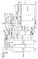
[実施の形態1]
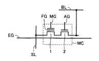
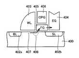
図1は、この発明の実施の形態1において用いられる半導体装置のメモリセルの電気的等価回路を概略的に示す図である。図1において、メモリセルMCは、フローティングゲートFGを有するメモリトランジスタ1と、メモリトランジスタ1と直列に接続されるアシストゲートトランジスタ(選択トランジスタ)2を含む。メモリトランジスタ1は、フローティングゲートFGとその上層に形成されるメモリゲートMGとの積層ゲート構造を有するNチャネルMOSトランジスタ(絶縁ゲート型電界効果トランジスタ)であり、そのソース不純物領域がソース線SLに結合される。アシストゲートトランジスタ2は、アシストゲートAGを有する単層ゲート構造のNチャネルMOSトランジスタであり、ビット線BLにその不純物領域が接続される。これらのアシストゲートトランジスタ2およびメモリゲートトランジスタ1の間には不純物領域は形成されない。[Embodiment 1]
FIG. 1 schematically shows an electrical equivalent circuit of a memory cell of a semiconductor device used in the first embodiment of the present invention. In FIG. 1, a memory cell MC includes a
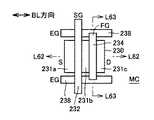
メモリセルMCは、さらに消去ゲートEGを有する。この消去ゲートEGは、メモリセルを分離する素子分離領域(STI(シャロー・トレンチ・アイソレーション)膜)表面に、列方向(ビット線延在方向)に沿って連続的に延在するように形成される。この消去ゲートEGとフローティングゲートFGの間で電荷を移動させ、フローティングゲートFGから電子を消去ゲート線EGに引抜くことにより、消去動作を行なう。このメモリセルMCの境界領域にビット線BLと平行に消去ゲートEGを埋込配線で配設することにより、メモリセルMCのレイアウト面積の増大を抑制する。 Memory cell MC further includes an erase gate EG. The erase gate EG is formed on the surface of an element isolation region (STI (shallow trench isolation) film) for isolating memory cells so as to continuously extend in the column direction (bit line extending direction). Is done. An erase operation is performed by moving charges between the erase gate EG and the floating gate FG and drawing electrons from the floating gate FG to the erase gate line EG. By disposing an erase gate EG as a buried wiring in the boundary region of the memory cell MC in parallel with the bit line BL, an increase in the layout area of the memory cell MC is suppressed.
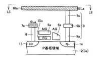
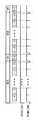
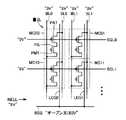
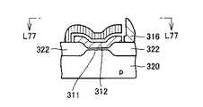
図2は、メモリセルの平面レイアウトを概略的に示す図である。図2において、Y方向(列方向)に沿って互いに間をおいてかつ各々Y方向に沿って連続的に延在するように活性領域3aおよび3bが配置される。活性領域3aおよび3b各々においては、図1に示すメモリトランジスタ1およびアクセストランジスタ2が形成される。 FIG. 2 schematically shows a planar layout of the memory cell. In FIG. 2,
活性領域3aおよび3bと直交する方向に、すなわちX方向(行方向)に連続的に延在してメモリゲート配線5a−5dおよびアシストゲート配線6a−6dがそれぞれ隣接して配置される。メモリゲート配線5a−5dがメモリゲートMGa−MGdを構成し、アシストゲート配線6a−6dがアシストゲートAGa−AGdを構成する。
メモリゲート配線5a−5dの間に、ソース線SLa−SLcをそれぞれ形成するメタル配線7a−7cがX方向に連続的に延在してかつ互いに間をおいて配置される。ソースメタル配線7a−7cは、それぞれソースコンタクト8により、下層の活性領域に形成される不純物領域に電気的に接続される。 Between the
活性領域3aおよび3b上にY方向に連続的に延在してビット線BLaおよびBLbをそれぞれ形成するメタル配線10aおよび10bがそれぞれ配設される。このビット線メタル配線10aおよび10bはそれぞれ、アシストゲートを構成するゲート配線6aおよび6bの間のビット線コンタクト9を介して活性領域3aおよび3bに形成される不純物領域に接続される。
また、活性領域3aおよび3bの間の素子分離領域には、後に説明するようにシャロー・トレンチ・アイソレーション膜が形成されており、このシャロー・トレンチ・アイソレーション膜上に、埋込消去ゲート配線層4aおよび4bがY方向に沿って連続的に延在して形成され、それぞれ消去ゲートEGaおよびEGbとして用いられる。活性領域3aおよび3bの間には、埋込消去ゲート配線層は設けられていない。2行のメモリセルに共通に消去ゲート線が共有される。 In addition, a shallow trench isolation film is formed in the element isolation region between the
図2に示す平面レイアウトにおいて、図2において破線ブロックで示すメモリセル領域MCRは、ビット線コンタクト9、アシストゲートAG、メモリゲートMG、ソース線コンタクト8および消去ゲートEGを含む。Y方向において隣接するメモリセルにおいてビット線コンタクト9およびソース線コンタクト8が共有され、メモリセルレイアウト面積を低減する。また、2行に配設されるメモリセルに共通に消去ゲート線を設けることにより、最小消去単位を2行のメモリセルに設定することができる。 In the planar layout shown in FIG. 2, a memory cell region MCR shown by a broken line block in FIG. 2 includes a
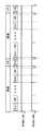
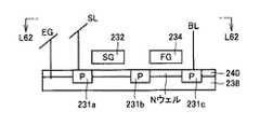
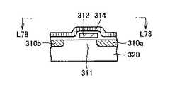
図3は、図2に示す線L3−L3に沿った断面構造を概略的に示す図である。図3において、P型半導体基板領域12表面に、互いに間をおいてN型不純物領域13および14が形成される。このP型半導体基板領域12は、図2に示す活性領域3aに対応する。 FIG. 3 schematically shows a cross-sectional structure taken along line L3-L3 shown in FIG. In FIG. 3, N-
不純物領域13は、ソース線コンタクト8を介してソース線SLaを形成するメタル配線7aに電気的に接続される。一方、不純物領域14は、ビット線コンタクト9を介してビット線BLaを形成するメタル配線10aに電気的に接続される。ビット線コンタクト9は、プラグ9aおよび9cと、これらのプラグ9aおよび9cの間の中間配線9bを含む。
不純物領域13および14の間の基板領域上に、フローティングゲートFGを構成する電荷蓄積層15とメモリゲートMGを形成するゲート配線5aが互いに整列してかつ積層して配置される。フローティングゲートFGおよびメモリゲートMGに隣接してアシストゲートAGを形成するゲート配線6aが配置される。アシストゲートAGは単に、下層の基板領域12表面に選択的にチャネルを形成する。 On the substrate region between
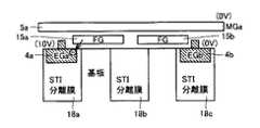
図4は、図2に示す線L4−L4に沿った断面構造を概略的に示す図である。線L4−L4に沿った領域おいては、メモリゲートMGaが、メタルゲート配線5aにより形成されており、その下部の基板領域表面には、チャネル領域が存在し、不純物領域は設けられていない。各活性領域(3a、3b)は、STI(シャロー・トレンチ・アイソレーション)分離膜18a、18bおよび18cにより互いに分離される。 FIG. 4 schematically shows a cross-sectional structure taken along line L4-L4 shown in FIG. In the region along the line L4-L4, the memory gate MGa is formed by the
活性領域(明確に示さず;正確にはメモリトランジスタのチャネル形成領域)表面上にフローティングゲートFGを構成する電荷蓄積層15aおよび15bが配置される。STI分離膜18aおよび18c表面に、上部に突出部を有する埋込配線層4aおよび4bが形成され、フローティングゲートを構成する電荷蓄積層15aおよび15bに、この突出部が隣接する。図4においては、中央のSTI分離膜18bにおいては、消去ゲートEGを構成する埋込配線層は形成されないが、形成されていてもよい。 Charge storage layers 15a and 15b constituting floating gate FG are arranged on the surface of the active region (not explicitly shown; precisely, the channel formation region of the memory transistor). Embedded wiring layers 4a and 4b having protrusions on the top are formed on the surfaces of the
図5は、各動作モード時におけるメモリゲートMG、ソース線SL、アシストゲートAGおよびビット線BL、および、消去ゲートEGへの各動作モード時の印加電圧を一覧にして示す図である。以下、図5に示す印加電圧を参照して、各動作モードについて説明する。 FIG. 5 is a diagram showing a list of voltages applied to the memory gate MG, the source line SL, the assist gate AG and the bit line BL, and the erase gate EG in each operation mode in each operation mode. Hereinafter, each operation mode will be described with reference to the applied voltage shown in FIG.
図6は、メモリセルMCへのデータ書込時の選択メモリセルへの印加電圧を示す図である。この場合、図5に示すように、選択メモリセルMCのメモリゲートMGへ10Vが印加され、ソース線SLには5Vが印加される。アシストゲートAGには1.5Vが印加され、ビット線BLは、0Vに設定される。図6においては示さない埋込消去ゲートEGはオープン状態または接地電圧(0V)に設定される。 FIG. 6 is a diagram showing a voltage applied to the selected memory cell at the time of data writing to the memory cell MC. In this case, as shown in FIG. 5, 10V is applied to the memory gate MG of the selected memory cell MC, and 5V is applied to the source line SL. 1.5V is applied to the assist gate AG, and the bit line BL is set to 0V. The embedded erase gate EG not shown in FIG. 6 is set to an open state or a ground voltage (0 V).
この状態においては、アシストゲートAGには1.5V程度の低い電圧が印加され、その下層の基板表面に比較的高抵抗のチャネルを形成する。ソース線SLから不純物領域13および14を介してビット線BLに電流が流れる。アシストゲートAG下部には、比較的高抵抗のチャネルが形成されており、この高抵抗のチャネル境界領域において高電界が発生し、この高電界により電子がエネルギを得てホットエレクトロンとなる。メモリゲートMGの高電圧により、この生成された電子(ホットエレクトロン)がフローティングゲートFGに注入される。これにより、メモリトランジスタのしきい値電圧が高くなる。 In this state, a low voltage of about 1.5 V is applied to the assist gate AG, and a relatively high resistance channel is formed on the surface of the underlying substrate. A current flows from the source line SL to the bit line BL through the
非選択メモリセルに対しては、メモリゲートMG、ソース線SL、アシストゲートAGは0Vに設定され、ビット線BLが1.5Vに設定される。非選択メモリゲートMGおよび非選択アシストゲートAGが0Vであり、チャネルは形成されず、電流は流れない。 For unselected memory cells, the memory gate MG, the source line SL, and the assist gate AG are set to 0V, and the bit line BL is set to 1.5V. The non-selected memory gate MG and the non-selected assist gate AG are 0V, no channel is formed, and no current flows.
ビット線BLを、非選択セルに対して1.5Vに設定するのは以下の理由による。すなわち、図2に示すように、アシストゲートAGを構成するアシストゲート配線とビット線BLとは直交する方向に配置される。したがって、選択行かつ非選択列のメモリセルにおいては、アシストゲートAGが選択状態の1.5Vである。ビット線BLを1.5Vに設定することにより、非選択メモリセルにおいてアシストゲートトランジスタのゲートおよびソース(アシストゲートAGおよび不純物領域14)の電位が等しくなり、チャネルは、アシストゲートAG下部に形成されず、不純物領域13および14間に電流は流れない。これにより、半選択状態のメモリセルに対するデータの書込を防止する。 The reason why the bit line BL is set to 1.5 V for the non-selected cells is as follows. That is, as shown in FIG. 2, the assist gate wiring constituting the assist gate AG and the bit line BL are arranged in a direction orthogonal to each other. Therefore, in the memory cell of the selected row and the non-selected column, the assist gate AG is 1.5 V in the selected state. By setting bit line BL to 1.5 V, the potentials of the gate and source (assist gate AG and impurity region 14) of the assist gate transistor are equalized in the non-selected memory cell, and the channel is formed below assist gate AG. In other words, no current flows between the
図7は、消去時のメモリセルへの印加電圧をその断面構造とともに示す図である。図5および図7に示すように、消去時においては、選択メモリセルおよび非選択メモリセルに関わらず、メモリゲートMG、ソース線SLは接地電圧(0V)に設定され、アシストゲートAGおよびビット線BLは開放状態(オープン状態)に設定される。選択メモリセルに対して埋込消去ゲートEGaに10Vを印加し、非選択メモリセルの消去ゲートEGbには0Vを印加する。この場合、図7に示すように、電荷蓄積層15aと埋込消去ゲートEGaの間に大きな電界が印加され、フローティングゲート15aから埋込消去ゲート配線4aにファウラーノルドハイム電流により電子が流出し、電荷蓄積層15aの蓄積電荷量が低減し、メモリトランジスタのしきい値電圧が小さくなる。一方、埋込消去ゲートEGbには0Vが印加され、フローティングゲートFGb(電荷蓄積層15b)と埋込ゲートEGbの間には、高電界は印加されず、電荷の移動は生じない。 FIG. 7 is a diagram showing a voltage applied to the memory cell at the time of erasing together with its cross-sectional structure. As shown in FIGS. 5 and 7, at the time of erasing, regardless of the selected memory cell and the unselected memory cell, the memory gate MG and the source line SL are set to the ground voltage (0 V), and the assist gate AG and the bit line are set. BL is set to an open state (open state). For the selected memory cell, 10V is applied to the embedded erase gate EGa, and 0V is applied to the erase gate EGb of the non-selected memory cell. In this case, as shown in FIG. 7, a large electric field is applied between the
この消去動作において、基板領域に正の消去高電圧を印加してフローティングゲートFGから電子を基板領域へと放出する場合、ソースおよびドレイン不純物領域により、基板領域からの高電圧が、同様、印加され、フローティングゲートFGと基板領域の間の結合容量が大きくなり、効率的に電荷(電子)を引抜けない。一方、埋込消去ゲートEGを利用する場合、単にSTI分離膜18aおよび18c表面に形成される埋込消去ゲート配線4aおよび4bの基板領域上部の突出部と対応のフローティングゲートFGとの間で電界が発生するだけであり、カップリングを小さくでき、低電圧で消去を行なうことができる。また、埋込消去ゲートEGは、STI分離膜18aおよび18c表面に形成されており、基板領域、ソース線およびビット線には、消去時の高電圧は印加されず、消費電力を低減することができる。また、後に説明するように、埋込消去ゲートは、ビット線、ソース線およびメモリゲート線と分離されており、埋込消去ゲートに消去電圧を印加した状態で、メモリセルに対してデータアクセスを行なうことができる。 In this erase operation, when a positive erase high voltage is applied to the substrate region and electrons are emitted from the floating gate FG to the substrate region, a high voltage from the substrate region is similarly applied by the source and drain impurity regions. The coupling capacitance between the floating gate FG and the substrate region is increased, and charges (electrons) are not efficiently extracted. On the other hand, when the embedded erase gate EG is used, an electric field is simply generated between the protruding portion above the substrate region of the embedded erase
図8は、メモリセルのデータ読出時の印加電圧および電流の流れる経路を概略的に示す図である。図5に示すように、メモリセルが選択セルの場合、ビット線BLに読出電圧1.0Vが印加され、アシストゲートAGに1.5Vが印加される。メモリゲートMGおよびソース線SLは、0Vに設定される。通常の読出時においては、埋込消去ゲートEGはオープン状態または接地電圧(0V)に設定される。 FIG. 8 schematically shows a path through which an applied voltage and current flow when reading data from a memory cell. As shown in FIG. 5, when the memory cell is a selected cell, a read voltage of 1.0 V is applied to the bit line BL, and 1.5 V is applied to the assist gate AG. Memory gate MG and source line SL are set to 0V. In a normal read operation, embedded erase gate EG is set to an open state or a ground voltage (0 V).
メモリセルのフローティングゲートFGが消去状態のときには、メモリトランジスタはデプレッション状態であり、下部にチャネルが形成され、ビット線BLからソース線SLに電流が流れる(アシストゲートAG下部にはチャネルが形成されている)。 When the floating gate FG of the memory cell is in the erased state, the memory transistor is in a depletion state, a channel is formed in the lower part, and a current flows from the bit line BL to the source line SL (a channel is formed in the lower part of the assist gate AG). )
一方、フローティングゲートFGが書込状態(プログラム状態)の場合、しきい値電圧は大きく、メモリトランジスタ(メモリゲート下部)の基板領域表面にはチャネルは、形成されない。この場合、ビット線BLからソース線SLへは、ほとんど電流が流れない。この消去状態を論理“1”および書込状態を論理“0”に対応付けると、ビット線BLを流れる電流を図示しないセンスアンプで検出することにより、メモリセルの記憶データを検出することができる。 On the other hand, when floating gate FG is in a write state (program state), the threshold voltage is large, and no channel is formed on the surface of the substrate region of the memory transistor (lower memory gate). In this case, almost no current flows from the bit line BL to the source line SL. When this erase state is associated with logic “1” and the write state is associated with logic “0”, the data stored in the memory cell can be detected by detecting the current flowing through the bit line BL with a sense amplifier (not shown).
非選択メモリセルにおいては、アシストゲートAGおよびビット線BLが0Vに設定される。選択行かつ非選択列のメモリセルにおいても、ビット線BLおよびソース線SLは同一電位であり、電流は流れず、データの読出は行なわれない。 In an unselected memory cell, assist gate AG and bit line BL are set to 0V. Also in the memory cells of the selected row and the non-selected column, the bit line BL and the source line SL are at the same potential, no current flows, and no data is read.
この埋込消去ゲートを用いて、フローティングゲートと埋込消去ゲートの間で電荷を移動させて消去を行なうメモリセルの構成の場合、書込電流は小さい(ソースサイド注入を行なっており、効率的に低消費電流(10μA程度)で書込を行なうことができる)。また、書込時に、電圧5V、10V、消去時に10Vの電圧が必要とされ、合計2種類の電源電圧を生成する電源回路が必要とされるだけである。また、消去および書込時の電流消費は小さく、消去および書込高電圧を生成する回路(チャージポンプ回路)のサイズを低減でき、応じて、レイアウト面積を低減することができる。 In the case of a memory cell configuration in which erasure is performed by moving charges between the floating gate and the embedded erase gate using this embedded erase gate, the write current is small (the source side injection is performed, In addition, writing can be performed with low current consumption (about 10 μA). Further, voltages of 5V and 10V are required at the time of writing and 10V at the time of erasing, and only a power supply circuit for generating a total of two types of power supply voltages is required. In addition, current consumption during erasing and writing is small, the size of a circuit (charge pump circuit) that generates erasing and writing high voltages can be reduced, and accordingly the layout area can be reduced.
本発明においては、この埋込消去ゲートを有するメモリセル構造を利用して、消去と並行して同一メモリブロック内でデータアクセスを行なう。 In the present invention, data access is performed in the same memory block in parallel with erasure by utilizing the memory cell structure having the embedded erase gate.
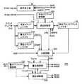
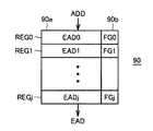
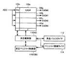
図9は、この発明の実施の形態1に従う半導体装置の全体の構成を概略的に示す図である。図9において、半導体装置は、メモリセルMCが行列状に配列されるメモリアレイ20を含む。この図9において、メモリアレイ20内において1つのメモリセルMCを代表的に示す。メモリセルMCは、ソース不純物領域13、ドレイン不純物領域14、埋込消去ゲートEGを構成する埋込消去ゲート配線4と、ウェル領域にウェル電圧WELLを印加するP型不純物領域21を含む。このウェル電圧WELLは、図9に示す構成においては接地電圧レベルに固定される。 FIG. 9 schematically shows an overall configuration of the semiconductor device according to the first embodiment of the present invention. In FIG. 9, the semiconductor device includes a
このメモリセルMCの基板領域上に、アシストゲートAG、フローティングゲートFGおよびメモリゲートMGが形成される。1行のメモリセルのアシストゲートAGはアシストゲート線AGLに接続され、1行のメモリセルのメモリゲートMGがメモリゲート線MGLに接続される。またソース線SLが不純物領域13に接続される。このソース線SLは、書込モード時に5Vの電圧が印加されるため、その電圧レベルが後に説明する行デコーダ28により設定される。1列のメモリセルの不純物領域14に共通にビット線BLが設けられる。 An assist gate AG, a floating gate FG, and a memory gate MG are formed on the substrate region of the memory cell MC. The assist gate AG of one row of memory cells is connected to the assist gate line AGL, and the memory gate MG of one row of memory cells is connected to the memory gate line MGL. Further, the source line SL is connected to the
この半導体装置は、さらに、外部からのアドレスADDを受けるアドレスレジスタ22と、アドレスレジスタ22からのアドレスおよび外部からの制御信号/WE、/CEおよび/OEを受けて、指定された動作モードを識別し、指定された動作に必要な動作制御を行なうコマンドレジスタ/制御回路24と、コマンドレジスタ/制御回路24からの動作モード指示に従って動作モードに応じた電圧を発生する電圧発生回路26を含む。 The semiconductor device further identifies an designated operation mode in response to an
制御信号/WEは、ライトイネーブル信号であり、制御信号/CEは、チップイネーブル信号でありこの半導体装置が選択されたことを示す。制御信号/OEは出力イネーブルであり、データ読出タイミングを与える。通常、これらの制御信号/WEおよび/CEの変化に応じて、動作モードを指定するコマンドおよびアクセス対象のメモリセルを指定するアドレスを取り込むタイミングが規定される。このコマンドは、アドレス入力ノードおよびデータ入力ノードを介して与えられる。 Control signal / WE is a write enable signal, and control signal / CE is a chip enable signal, indicating that this semiconductor device has been selected. Control signal / OE is an output enable and provides data read timing. Normally, the timing for fetching the command for designating the operation mode and the address for designating the memory cell to be accessed are defined in accordance with changes in these control signals / WE and / CE. This command is given via an address input node and a data input node.
電圧発生回路26は、消去モード時には消去動作に必要な電圧(10V)を生成し、書込モード時においては、5Vおよび10Vおよび1.5Vの電圧を生成する。読出時においては、アシストゲートへの電圧1.5Vおよびビット線BLに印加される1.0Vの電圧を生成する。
半導体装置はさらに、行選択を行う行デコーダ28、列選択を行う列デコーダ30および列選択ゲート回路32と消去ゲート電圧を設定するEG制御回路34とを含む。行デコーダ28は、アドレスレジスタ22からのアドレス信号に従ってメモリセルアレイ24の選択行に対応するアシストゲート線AGLおよびメモリゲート線MGLへ、電圧発生回路26から与えられた電圧を伝達する。この行デコーダ28は、ソース線デコーダ28を含み、データ書込時選択列の書込対象のソース線に5Vの書込電圧を伝達する。 The semiconductor device further includes a
列デコーダ30は、アドレスレジスタ22からの列アドレス信号をデコードし、メモリアレイ20の列を対応するビット線を選択する列選択信号を生成するとともに、電圧発生回路26からの電圧レベルの列選択信号を生成する。列選択ゲート回路32は、列デコーダ30からの列選択信号に従って選択列のビット線を選択する。 The
EG制御回路34は、消去動作時、アドレスレジスタ22からのアドレス信号に従って消去対象の消去ゲート線EGLへ、電圧発生回路26からの消去電圧を伝達する。 The
このEG制御回路34は、消去時、電圧発生回路26からの消去電圧を伝達された書込消去ゲート線EGL上に供給する。行デコーダ28および列デコーダ30は、EG制御回路34からの消去高電圧印加期間中に、並行してメモリセル選択を行ない、消去ベリファイのためのメモリセルデータ読出を実行する。 The
この半導体装置は、さらに、メモリセルのデータを読出すセンスアンプ36と、選択メモリセルにデータの書込を行なうデータ書込ドライバ38と、外部との間でデータDQを送受する入出力バッファ40を含む。データ書込ドライバ38およびセンスアンプ36へは、アドレスレジスタ22からのアドレスが与えられ、複数の列(1I/Oあたり)のうち1つの列を選択してデータの書込および読出を実行する。データ書込ドライバ38へは、また、電圧発生回路26からの書込電圧が与えられ、データ書込ドライバ38により、ビット線書込電圧を選択列へ伝達する。 This semiconductor device further includes a
データ書込ドライバ38により、“0”データの書込を行なう場合、ビット線BLの電圧が0Vに設定され、データ“0”が書込まれる。一方、データ“1”を格納する場合には、ビット線BLに1.5Vの電圧が印加され、選択メモリセルは、消去状態の低しきい値電圧状態に維持される。 When “0” data is written by the data write
入出力バッファ40は、データ書込時には、外部からのデータDQから内部書込データを生成してデータ書込ドライバ38へ伝達し、データ読出時には、センスアンプ36からの内部読出データをバッファ処理して外部出力データDQを生成する。データ出力タイミングが制御信号/OEにより決定される。 Input /
このコマンドレジスタ/制御回路20および電圧発生回路26を用いて各動作モードに応じた内部電圧を生成するとともに、内部動作を制御する。コマンドレジスタ/制御回路24は、たとえばシーケンスコントローラで構成され、消去、書込および読出に必要な内部動作をシーケンスコントローラに設定されたシーケンスに従って順次制御する。 The command register /
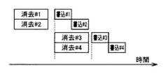
図10は、図9に示す半導体装置の消去時の動作を示すフロー図である。以下、図10を参照して、図9に示す半導体装置の消去動作について説明する。 FIG. 10 is a flowchart showing an operation at the time of erasing of the semiconductor device shown in FIG. Hereinafter, the erasing operation of the semiconductor device shown in FIG. 9 will be described with reference to FIG.
まず、外部から消去動作を指示するコマンドおよび消去対象のメモリセル領域を示すアドレスが与えられる(ステップS1)。このコマンドおよびアドレスに従って図9に示すコマンドレジスタ/制御回路24は、電圧発生回路26に、消去モード指示ERSを与え、電圧発生回路26に消去動作に必要な電圧を発生させる。 First, a command for instructing an erase operation and an address indicating a memory cell area to be erased are given from the outside (step S1). In accordance with this command and address, command register /
行デコーダ28は、消去モード時においては、アシストゲート線AGLおよびメモリゲート線MGLを、それぞれ、オープン状態(または0V)および0Vに設定する。列デコーダ30の出力信号は全て非選択状態であり、列選択ゲート回路32は、ビット線BLを全て、オープン状態に維持する。 In the erase mode,
この状態で、選択されたメモリセルの消去ゲート線EGLに消去高電圧(消去パルス)を印加する(ステップS2)。すなわち、図9に示すEG制御回路34は、電圧発生回路26からの消去高電圧を、選択メモリセルに対して配置された埋込消去ゲート線EGLへ伝達する。 In this state, an erase high voltage (erase pulse) is applied to the erase gate line EGL of the selected memory cell (step S2). That is, the
この消去パルスを印加した状態で、次いで消去対象のメモリセルのデータの読出を行い、メモリセルが消去状態、すなわち低しきい値電圧状態にあるかを識別する(ステップS3)。この消去ベリファイにおいて非消去状態のメモリセルが存在する場合、再びステップS2からの消去パルス印加ステップを実行する。一方、ステップS3において、消去対象のメモリセル全てが、消去状態と判定されると、消去動作が完了する。 In a state where the erase pulse is applied, data in the memory cell to be erased is then read to identify whether the memory cell is in an erased state, that is, a low threshold voltage state (step S3). If there is a non-erased memory cell in this erase verify, the erase pulse application step from step S2 is executed again. On the other hand, when it is determined in step S3 that all memory cells to be erased are in the erased state, the erase operation is completed.
通常、消去高電圧はたとえば10Vの電圧レベルである。この消去電圧は、電圧発生回路26においてチャージポンプ回路を用いて発生されるのが一般的である。したがって、消去高電圧の消去開始時の所定レベルへの立上げおよび消去停止時の所定レベルへの立下げに、数100μs程度の時間が必要である。この立下げ時間を利用してメモリセルデータの読出を行なって消去ベリファイを行なうことができ、消去時間を短くすることができる。特に、消去ゲート線EGLを選択状態のHレベルに維持した状態でも消去ベリファイを実行することができ、消去時間を短くすることができる。この場合、選択トランジスタ(アシストゲートAG)が存在するため、メモリトランジスタは、過消去状態(デプレッション状態)にあっても特に問題は生じず、消去パルス印加時にメモリセルのデータの読出を行なって、通常よりも長い期間消去パルスが印加される状態が生じても特に問題は生じない。 Usually, the erase high voltage is, for example, a voltage level of 10V. This erase voltage is generally generated in the
なお、1回目の消去での消去ベリファイ時に、1ビットでも非消去状態のメモリセルが存在すると、消去対象のメモリセルに対して再度、2回目の消去パルス(消去高電圧)が印加される。 If there is a non-erased memory cell even with one bit at the time of erase verify in the first erase, the second erase pulse (erase high voltage) is applied again to the memory cell to be erased.
図11は、図10に示す消去動作を具体的に示すタイミング図である。以下、図11を参照して、図9に示す半導体装置の消去動作について説明する。 FIG. 11 is a timing diagram specifically showing the erase operation shown in FIG. Hereinafter, the erasing operation of the semiconductor device shown in FIG. 9 will be described with reference to FIG.
図11において、外部からの制御信号/WEおよび/CEをともに一旦立下げてから立上げると、データ端子DQおよびアドレス端子ADDから与えられた信号が、コマンドとして内部へ取込まれ、コマンドレジスタ/制御回路24により取込んだコマンドに従って動作モード(消去モード)の識別が行なわれる。 In FIG. 11, when both external control signals / WE and / CE are once lowered and then raised, signals applied from data terminal DQ and address terminal ADD are taken into the inside as commands, and command register / The operation mode (erase mode) is identified according to the command fetched by the
次に、制御信号/WEおよび/CEの立上がりから次の立下がりに従って、アドレスADDがアドレスレジスタ22に取込まれて消去対象のメモリセルが指定される。この後、制御信号/WEおよび/CEをHレベルに立上げると、消去モードが開始される。すなわち、コマンドレジスタ/制御回路24は、制御信号/WEおよび/CEが2回立上げられると、コマンドにより指定された動作モードに入る。この場合、電圧発生回路26に消去モード指示ERSをイネーブルして与え、消去に必要な電圧(消去高電圧)を発生させる。消去モードにおいては、EG制御回路34により、消去対象として指定されたメモリセルの埋込消去ゲート線EGLへは、消去高電圧(+10V)の消去パルスが印加される。この消去パルスが印加され所定期間が経過すると、内部で消去ベリファイ読出を行なう。すなわち、所定時間経過後、所定の時間間隔で、消去ベリファイ読出指示VREADが、イネーブルされ、行デコーダ28および列デコーダ30および列選択ゲート回路32を用いて、埋込消去ゲート線EGLに消去電圧を与えた状態で、メモリゲート線MGLおよびビット線BLに読出電圧を供給する。ビット線電流に従って選択メモリセルのデータをセンスアンプ36で読出し、コマンドレジスタ/制御回路24において、読出したメモリセルが消去状態にあるかの識別を行なう。このベリファイ動作を、各メモリセルに対して順次実行する。 Next, in accordance with the next fall from the rise of control signals / WE and / CE, address ADD is taken into
この1回目の消去に対するベリファイ(VR)により、消去不良(消去フェイル)と判断されると、引続き、消去パルスを所定期間印加した後、再度消去ベリファイを実行する(消去高電圧を印加した状態で)この2回目の消去に対するベリファイにおいて全ビット消去完了と判定されると(消去パスと判定されると)、消去モードERSをディスエーブルし、EG制御回路34から消去ゲート線EGLへの消去高電圧の印加を停止する。この消去パルスの印加および消去ベリファイは、消去ベリファイにおいて消去パスと判定されるまで、繰返し実行される。 If it is determined that erase failure (erase failure) is caused by verify (VR) for the first erase, erase erase is subsequently applied for a predetermined period, and then erase verify is executed again (with an erase high voltage applied). When it is determined that all bits have been erased in the verify for the second erase (determined as an erase pass), the erase mode ERS is disabled and the erase high voltage from the
消去パルスの印加期間の間に、複数の消去対象のメモリセルの逐次ベリファイ読出を行なうことができる。したがって、この消去パルスが完全に接地電圧レベルに低下するまでの期間を待つ必要なく、ベリファイ動作を開始することができ、消去時間を短縮することができる。この場合、1回目の消去ベリファイ読出を行なうまでの期間として、消去に必要な期間が確保されればよい。消去ベリファイ時においては、少なくとも1ビットの未消去状態のメモリセルが存在する場合、消去対象のメモリセルに対し引続き消去パルスを印加する。したがって、最初の消去ベリファイを消去パルス印加中に行なうメモリセルの消去パルス印加期間が仮に不十分であっても、消去ベリファイ期間において消去パルスが印加される。したがって、次の消去パルス印加後、この最初の消去ベリファイ時に未消去状態と識別されるメモリセルでも、確実に、消去状態に設定することは可能であり、全体として消去時間の増大は、十分に抑制することができる。 During the erase pulse application period, a plurality of memory cells to be erased can be sequentially verified and read. Therefore, the verify operation can be started without waiting for a period until the erase pulse is completely lowered to the ground voltage level, and the erase time can be shortened. In this case, a period necessary for erasure may be ensured as a period until the first erase verify read is performed. At the time of erase verify, if there is an unerased memory cell of at least 1 bit, an erase pulse is continuously applied to the memory cell to be erased. Therefore, even if the erase pulse application period of the memory cell in which the first erase verify is performed during application of the erase pulse is insufficient, the erase pulse is applied in the erase verify period. Therefore, even after the next erase pulse is applied, even the memory cell that is identified as the unerased state at the time of the first erase verification can be surely set to the erased state. Can be suppressed.
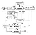
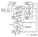
図12は、メモリセルMCの消去および消去ベリファイ読出に関連する部分の構成を概略的に示す図である。コマンドレジスタ/制御回路24は、コマンドをデコードするコマンドデコーダ40と、コマンドデコーダ40のデコードしたコマンドを格納するコマンドレジスタ41と、コマンドレジスタ41に格納される消去コマンドに従って消去動作を制御する消去制御部42と、消去ベリファイを行なう消去ベリファイブ43を含む。 FIG. 12 schematically shows a structure of a portion related to erasure of memory cell MC and erase verify read. The command register /
コマンドデコーダ40は、外部からの制御信号/WEおよび/CEおよび/OEに従って、アドレスADDおよびデータDQをコマンドとして受けてデコードする。
消去制御部42は、コマンドレジスタ41に格納された消去コマンドに従って消去指示ERSをイネーブルして消去動作モードを指示するとともに消去ベリファイ時には所定の間隔で消去読出指示VREADをアサート(活性化)し、消去動作および消去ベリファイ読出動作の制御および消去ベリファイ制御部43のベリファイ動作を制御する。この消去制御部42は、たとえば消去制御シーケンスコントローラで構成され、消去コマンドに従って所定のシーケンスで消去指示ERSおよび消去ベリファイ読出指示VREADを所定のタイミングでイネーブルする。 The erase
消去ベリファイ制御部43は、消去制御部42により動作制御され、センスアンプ36に含まれるセンスアンプ回路48からのベリファイ読出データDOを受け、このベリファイ読出データDOが消去状態を示す論理値であるかを判別する。 Erase verify
電圧発生回路26は、消去高電圧発生回路46と、AG読出電圧発生回路45とを含む。消去高電圧発生回路46は、消去制御部42からの消去動作指示ERSの活性化時(アサート時)、消去高電圧VPEG(+10V)を生成する。一方、消去読出および消去ベリファイおよび書込時において、1.5Vまたは0Vの電圧がアシストゲートAGに印加されるだけであり、AG読出電圧発生回路45は、たとえば1.5Vのアシストゲート電圧Vagを常時生成する。
EG制御回路34は、EG線選択回路47を含む。このEG線選択回路47は、消去動作時消去制御部42によりイネーブルされ、アドレス信号ADDに従って消去対象のメモリセルの埋込消去ゲート線EGLを選択し、該選択された埋込消去ゲート線EGLに、消去高電圧発生回路46からの消去高電圧VPEGを伝達する。 The
消去動作時、行デコーダ28は、消去ベリファイ読出指示VREADがアサートされると、アドレス信号ADDに従って消去対象のメモリセルに対して配置されるアシストゲート線AGLにアシストゲート電圧Vagを伝達する。このとき、メモリゲート線MGLは、0Vに設定される。行デコーダ28により選択された1行のメモリセルのうち、図9に示す列選択ゲート回路32が列デコーダ30からの列選択信号に従って選択メモリセルのビット線BLをセンスアンプ36に結合する。センスアンプ36は、センスアンプ回路48を含み、読出電流Ireadを選択列のビット線BLに伝達し、参照電流REFとの間で大小比較を行なってベリファイ読出データDOを生成し、消去ベリファイ制御部43へ与える。 During the erase operation, when the erase verify read instruction VREAD is asserted, the
消去ベリファイ制御部43は、センスアンプ36からの内部読出データDOが消去状態の論理値“1”であるかの判別を行い、消去不良ビットが存在すると、消去不良ビットの存在を消去制御部42に伝達する。全ビットが消去状態のときには、消去完了を消去制御部42に通知する。この消去ベリファイ制御部43からの消去結果通知に従って、消去動作の継続および完了(消去パルスの継続印加および印加停止)を実行する。 The erase verify
消去ベリファイ動作時、消去高電圧を埋込消去ゲート線EGLに与えた場合、メモリセルMCにおいて、フローティングゲートFGと埋込消去ゲート線EGLの間で電子が、ファウラーノルドハイム電流の形態で引抜かれる。このフローティングゲートFGおよび埋込消去ゲート線EGLは、ソース線SL、メモリゲートMGおよびアシストゲートAGおよびビット線BLとすべて電気的に分離されている。したがって、この状態で、アシストゲートAGにベリファイ読出電圧Vagを印加してビット線BLとソース線SLの間に、メモリセルMCの記憶データに応じた電流を流しても、何ら消去動作には影響を及ぼさず、正確にメモリセルMCのメモリトランジスタのしきい値電圧に応じた電流を流すことができる。 When an erase high voltage is applied to the embedded erase gate line EGL during the erase verify operation, electrons are extracted in the form of a Fowler-Nordheim current between the floating gate FG and the embedded erase gate line EGL in the memory cell MC. . Floating gate FG and embedded erase gate line EGL are all electrically isolated from source line SL, memory gate MG, assist gate AG and bit line BL. Therefore, even if a verify read voltage Vag is applied to the assist gate AG in this state and a current corresponding to the data stored in the memory cell MC is passed between the bit line BL and the source line SL, the erase operation is not affected. Current corresponding to the threshold voltage of the memory transistor of the memory cell MC can be made to flow accurately.
図13は、このメモリトランジスタのしきい値電圧とメモリセルを流れる電流の対応を概略的に示す図である。消去状態においては、メモリトランジスタはしきい値電圧Vth0を有し、メモリゲートMGに印加される電圧Vmgが0Vであっても、メモリトランジスタにはチャネルが形成される。一方、メモリトランジスタが書込状態のときには、このメモリトランジスタは、しきい値電圧Vth1を有し、メモリゲート電圧Vmgが0Vの場合、電流は流れない。直列に接続されるアシストゲートAGを選択することにより、メモリトランジスタのしきい値電圧の状態に応じた読出電流がビット線BLソース線SLとの間に流れ、センスアンプ36において、ビット線電流と参照電流Irefとの大小に応じて、消去状態および書込状態を識別することができる。 FIG. 13 is a diagram schematically showing the correspondence between the threshold voltage of the memory transistor and the current flowing through the memory cell. In the erased state, the memory transistor has a threshold voltage Vth0, and a channel is formed in the memory transistor even if the voltage Vmg applied to the memory gate MG is 0V. On the other hand, when the memory transistor is in a write state, this memory transistor has threshold voltage Vth1, and no current flows when memory gate voltage Vmg is 0V. By selecting the assist gates AG connected in series, a read current corresponding to the threshold voltage state of the memory transistor flows between the bit line BL and the source line SL. The erase state and the write state can be identified according to the magnitude of the reference current Iref.
また、消去状態においては、メモリトランジスタは、デプレッション状態にある。しかしながら、アシストゲートトランジスタ(選択トランジスタ)により、メモリセルの選択/非選択がデータ書込/読出時に行なわれるため、この消去状態、すなわちデプレッション状態にメモリトランジスタがあっても特に、問題は生じず、また、消去の制御が容易となる(デプレッション状態が許容されるため)。 In the erased state, the memory transistor is in a depletion state. However, since the memory cell is selected / unselected at the time of data writing / reading by the assist gate transistor (select transistor), even if there is a memory transistor in this erase state, that is, the depletion state, no problem occurs. In addition, erasure control is facilitated (because the depletion state is allowed).
以上のように、この発明の実施の形態1に従えば、埋込消去ゲート線を用いて消去を行なっており、この消去ゲートは、ビット線、ソース線、ウェルおよびメモリゲートと分離されており、消去電圧印加と並行して消去ベリファイ読出を行なうことができる。これにより、消去に要する時間を短縮することができる。 As described above, according to the first embodiment of the present invention, erasing is performed using the embedded erase gate line, and this erase gate is separated from the bit line, source line, well and memory gate. The erase verify read can be performed in parallel with the erase voltage application. Thereby, the time required for erasing can be shortened.
[実施の形態2]
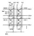
図14は、この発明の実施の形態2に従う半導体装置の全体の構成を概略的に示す図である。図14に示す半導体装置は、以下の点で、図9に示す半導体装置とその構成が異なる。すなわち、メモリアレイ20において、複数の埋込消去ゲート線EGLAおよびEGLBにより、メモリアレイ20は複数の列ブロックに分割される。埋込消去ゲート線EGLA(EG(0))がメモリセルMCaの埋込消去ゲートEGに結合され、埋込消去ゲート線EGLB(EG(1))が、メモリセルMCbの埋込消去ゲートEGに結合される。メモリセルMCaおよびMCbは、それぞれビット線BL(0)およびBL(1)に結合される。[Embodiment 2]
FIG. 14 schematically shows a whole structure of the semiconductor device according to the second embodiment of the present invention. The semiconductor device shown in FIG. 14 differs from the semiconductor device shown in FIG. 9 in the following points. That is, in
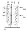
メモリアレイ20は、単一バンク構造であり、ある行のメモリセルに対するデータアクセス(読出または書込)時、別の行のメモリセルに対して並行してデータアクセスはできない。
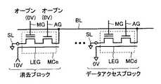
EG制御回路44は、埋込消去ゲート線単位で、メモリアレイ20における消去を実行する。ここで、メモリアレイ20が、列ブロックに分割されているのは、埋込消去ゲート線は、ビット線と平行に配設されているためである。したがって、消去対象のメモリセルMCaが消去実行状態のとき、この消去対象のメモリセルMCaと同一行のメモリセルMCbは埋込消去ゲート線は非選択状態であり、一方、アシストゲート線AGLはオープン状態である。メモリゲート線MGLおよびソース線SLは接地電圧レベルであり、ビット線BL(0)はフローティング状態である。このとき、アシストゲート線AGLを選択状態へ駆動して、この消去非対象のメモリセルMCbに対するデータの読出を実行する。この図14に示す半導体装置の他の構成は、図9に示す半導体装置の構成と同じであり、対応する部分には同一参照番号を付し、その詳細説明は省略する。 The
図15は、図14に示す列選択ゲート回路32の構成を、関連するメモリセルMC(0)およびMC(1)の接続態様とともに示す図である。メモリセルMC(0)は、埋込消去ゲート線EGL(0)に接続される消去ゲートEG(0)を有し、メモリセルMC(1)は、埋込消去ゲート線EGL(1)に接続される消去ゲートEG(1)を有する。メモリセルMC(0)およびMC(1)に共通に、メモリゲート線MGL(0)およびアシストゲート線AGL(0)が設けられる。メモリセルMC(0)はビット線BL(0)を介して列選択ゲート回路32に含まれるY選択ゲートYG0に結合され、メモリセルMC(1)は、ビット線BL(1)を介してY選択ゲートYG1に結合される。これらのY選択ゲートYG0およびYG1は、それぞれ、列選択信号SG(0)およびSG(1)に応答して選択的に導通し、導通時、対応のビット線BL(0)およびBL(1)を内部読出データ線RDに結合する。この内部読出データ線RDはセンスアンプ36に含まれるセンスアンプ回路48に結合される。このセンスアンプ回路48は、図12に示すセンスアンプ回路48と同じであり、内部読出データ線RDを流れる電流と参照電流IREFとを差動増幅して内部読出データDOを生成する。 FIG. 15 is a diagram showing the configuration of column
今、図15においてメモリセルMC(0)が消去対象のメモリセルであり、メモリセルMC(1)が読出対象のメモリセルであるとする。ここで、読出対象のメモリセルは、外部からデータアクセスが要求されたメモリセルである。 In FIG. 15, it is assumed that the memory cell MC (0) is a memory cell to be erased and the memory cell MC (1) is a memory cell to be read. Here, the memory cell to be read is a memory cell for which data access is requested from the outside.
図16は、図14および図15に示す半導体装置の消去動作および読出動作を並行して実行するときの動作タイミングを示す図である。以下、図16を参照して、図14および図15に示す半導体装置の消去時のデータ読出動作について説明する。 FIG. 16 is a diagram showing operation timings when the erase operation and read operation of the semiconductor device shown in FIGS. 14 and 15 are executed in parallel. Hereinafter, with reference to FIG. 16, a data read operation at the time of erasing of the semiconductor device shown in FIGS. 14 and 15 will be described.
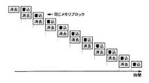
消去時においては、メモリゲート線MGL(0)およびアシストゲート線AGL(0)はともにオープン状態である。この状態で、埋込消去ゲート線EGL(0)に消去高電圧が印加され、消去対象のメモリセルMC(0)の埋込消去ゲートEG(0)の電圧レベルが10Vの高電圧レベルに設定されて、メモリセルMC(0)における消去が実行される。このとき、埋込消去ゲート線EGL(1)は非選択状態またはオープン状態の接地電圧レベルであり、メモリセルMC(1)に対しては何ら消去は行なわれない。消去電圧を埋込消去ゲートAG(0)に印加した状態で、埋込消去ゲート線EGL(1)に接続されるメモリセルMC(1)等のメモリセルの読出を実行する。 At the time of erasing, both memory gate line MGL (0) and assist gate line AGL (0) are in an open state. In this state, an erase high voltage is applied to the embedded erase gate line EGL (0), and the voltage level of the embedded erase gate EG (0) of the memory cell MC (0) to be erased is set to a high voltage level of 10V. As a result, erasure in memory cell MC (0) is executed. At this time, the embedded erase gate line EGL (1) is at the ground voltage level in the non-selected state or in the open state, and no erasure is performed on the memory cell MC (1). Reading of a memory cell such as the memory cell MC (1) connected to the embedded erase gate line EGL (1) is executed with the erase voltage applied to the embedded erase gate AG (0).
すなわち、アシストゲート線AGL(0)およびY選択信号SG(1)を選択状態に駆動し、メモリセルMC(1)のデータの読出を実行する。所定の間隔で、アシストゲート線AGL(i)を最終のアシストゲート線AGL(n)まで、順次選択する。このときまた、Y選択ゲートYG1を列選択信号SG(1)に従って選択状態に駆動する。これにより、埋込消去ゲート線EGL(1)に対応して配置されるメモリセルのデータを、順次読出すことができる。埋込消去ゲート線EGL(1)に対するメモリセルのデータの読出完了後、次いで、アシストゲート線AGL(0)を選択状態へ駆動するとともに、Y選択信号SG(0)を選択し、消去対象のメモリセルMC(0)、…のベリファイ読出を順次、消去高電圧を立ち下げる前に、開始する。 That is, assist gate line AGL (0) and Y selection signal SG (1) are driven to a selected state, and data is read from memory cell MC (1). The assist gate lines AGL (i) are sequentially selected up to the final assist gate line AGL (n) at predetermined intervals. At this time, the Y selection gate YG1 is driven to the selected state in accordance with the column selection signal SG (1). Thereby, data of memory cells arranged corresponding to embedded erase gate line EGL (1) can be read sequentially. After the memory cell data is read from the embedded erase gate line EGL (1), the assist gate line AGL (0) is driven to the selected state, and the Y selection signal SG (0) is selected to erase the data to be erased. Verify reading of the memory cells MC (0),... Is started sequentially before the erase high voltage is lowered.
したがって、消去高電圧を印加した状態で、データアクセス(外部読出)を行なうことができ、通常のフラッシュメモリのサスペンドモード動作のように、一旦、消去高電圧の印加を停止してビット線等の内部電圧が安定した後に外部からデータアクセスを行なう必要がない。これにより、高速のデータアクセスを行なうことができる、また、実施の形態1と同様、ベリファイと消去を並行して実行することが可能であり、消去に要する時間も短縮することができる。 Therefore, data access (external reading) can be performed with the erase high voltage applied, and the application of the erase high voltage is temporarily stopped and the bit line or the like is temporarily stopped as in the normal suspend mode operation of the flash memory. There is no need to externally access data after the internal voltage has stabilized. As a result, high-speed data access can be performed, and verification and erasure can be performed in parallel as in the first embodiment, and the time required for erasure can be shortened.
図17は、この発明の実施の形態2における半導体装置のメモリアレイ20の一般的構成を概略的に示す図である。図17においてメモリアレイ20は、複数の列ブロックCB0−CBnに分割される。これらの列ブロックCB0−CBnそれぞれに対応して埋込消去ゲート線EGL0、EGL1、…EGLnが設けられる。消去は、列ブロック単位で実行される。これらの列ブロックCB0−CBnに共通にアシストゲート線AGLおよびメモリゲート線MGLが配設される。列ブロックCB0−CBnそれぞれに、Y選択ゲートYG1、YG2、…YGnが設けられる。これらのYゲートYG1−YGnは、それぞれブロック選択信号SG0、SG1、…SGnに従って対応の列ブロックの選択列を内部読出データ線RDを介してセンスアンプへ結合する。 FIG. 17 schematically shows a general configuration of
この図17に示すアレイ構成においては、1つの列ブロックCBiにおいて消去が埋込消去ゲート線EGLiの印加電圧に従って実行されているとき、他の列ブロックにおいてデータの読出を行ない、また、消去ブロックにおいて消去動作と並行してベリファイ動作を行なうことができる。 In the array configuration shown in FIG. 17, when erasure is executed in one column block CBi in accordance with the voltage applied to embedded erase gate line EGLi, data is read out in the other column block. A verify operation can be performed in parallel with the erase operation.
なお、列ブロックCB0−CBnそれぞれにおいて、複数列にわたってビット線が配設される。この場合、ビット線各々に対して列選択ゲートが配置され、列選択信号に従ってビット線が選択され、この選択列のビット線がブロック選択信号SG0−SGnに従って対応のY選択ゲートにより選択されて内部読出データ線RDに結合される。 In each of the column blocks CB0 to CBn, bit lines are arranged over a plurality of columns. In this case, a column selection gate is arranged for each bit line, a bit line is selected according to a column selection signal, and a bit line of this selected column is selected by a corresponding Y selection gate according to block selection signals SG0-SGn. Coupled to read data line RD.
図18は、図14に示すコマンドレジスタ/制御回路24の構成を概略的に示す図である。図18に示すコマンドレジスタ/制御回路24において、コマンドレジスタとして、消去コマンドを格納する消去コマンドレジスタ41eと読出コマンドを格納する読出コマンドレジスタ41rとが設けられる。消去コマンドレジスタ41eからの消去コマンド(消去指示)が消去制御部42へ与えられる。また、消去対象の列ブロックを指定する消去ブロックアドレスを格納する消去ブロックアドレスレジスタ50が設けられる。 FIG. 18 schematically shows a structure of command register /
消去制御部42は、消去モードが指定されたとき、消去列ブロックを特定する列ブロックアドレスを消去ブロックアドレスレジスタ50に格納する。 When the erase mode is designated, the erase
消去制御部42は、また、消去ベリファイ動作を制御する消去ベリファイ制御部43の動作を制御する。このコマンドレジスタ/制御回路24において、また、比較回路52および読出制御部54が設けられる。比較回路52は、読出コマンドレジスタ41rに読出コマンドが格納され、この読出コマンドレジスタ41rからデコードされた読出コマンドとして読出指示Creadが与えられ、かつ消去制御部42からの消去モード指示ERSが与えられると、消去ブロックアドレスレジスタ50の格納ブロックアドレスと外部からのアドレス信号ADDのブロックアドレスとを比較する。 The erase
読出制御部54は、この比較回路52の出力信号が不一致を示すとき、読出モードイネーブル信号READをイネーブルする。読出制御部54からの読出モードイネーブル信号READは、消去制御部42へ与えられ、消去制御部42は、この読出モードイネーブル信号READのアサート時(活性化時)、ベリファイ動作を禁止状態に設定して、消去動作を継続的に実行する。 The
比較回路52がアドレスの一致を検出した場合には、この読出動作は消去ブロックに対して実行されるため、データの外部読出は停止され、読出動作モードイネーブル信号READは非活性状態に維持される。これにより、消去ブロックと別のブロックに対し外部からデータの読出アクセスを行なうことができる。 When
なお、このデータ読出時、外部からのアドレスをアドレスレジスタ22に格納し、このアドレスレジスタ22に格納されたアドレスを先頭アドレスとして、順次内部アドレスを生成して、選択ブロックの行(アシストゲート線)が順次選択されてもよい。このとき、列選択信号は、選択ブロックにおいて、同じ列を選択するように固定されてもよい。 At the time of this data reading, an external address is stored in the
図19は、図14に示す行デコーダ28、列デコーダ30およびEG制御回路34の構成をより具体的に示す図である。図19において、行デコーダ28は、アシストゲート線デコーダ56、メモリゲート線デコーダ58、およびソース線デコーダ59を含む。アシストゲート線デコーダ56は、読出モードイネーブル信号READ、消去モード指示ERSおよびベリファイ読出モード指示VREADに従って、データ読出モードにおいては、アドレス信号ADDに含まれるXアドレス信号ADXをデコードし、選択行のアシストゲート線AGLへ所定の電圧(Vag)を伝達する。 FIG. 19 is a diagram more specifically showing the configuration of
消去モード時においては、このアシストゲート線デコーダ56はディスエーブルされ、アシストゲート線AGLを開放状態または接地電圧(0V)レベルに設定する。アシストゲート線デコーダ56のアシストゲート線ドライバは、アシストゲート線を開放状態に設定する構成の場合、3値ドライバで構成され、消去モード時、非選択アシストゲート線ドライバは、出力ハイインピーダンス状態に設定される。 In the erase mode, assist
メモリゲート線デコーダ58も同様、消去モード指示ERS、読出モードイネーブル信号READ、およびベリファイ読出モードイネーブル信号VREADに従ってアドレス信号ADXをデコードし、メモリゲート線MGLに所定の電圧を印加する。このメモリゲート線デコーダ58は、消去動作モード時には、メモリゲート線MGLを開放状態(オープン状態)または接地電圧(0V)に設定し、ベリファイ読出およびデータアクセス読出時においては、メモリゲート線MGLを接地電圧レベルに維持する。メモリゲート線デコーダ58は、データ書込時において、選択行のメモリゲート線MGLに書込高電圧を印加する。 Similarly, memory
ソース線デコーダ59は、消去モード指示ERS、読出モードイネーブル信号READ、およびベリファイ読出モードイネーブル信号VREADに従ってアドレス信号ADXをデコードし、書込モード時、選択行のソース線SLへ書込高電圧(5V)を伝達し、それ以外の動作モード時には、ソース線SLを接地電圧レベルに維持する。 Source line decoder 59 decodes address signal ADX in accordance with erase mode instruction ERS, read mode enable signal READ, and verify read mode enable signal VREAD, and writes a high voltage (5 V) to source line SL of the selected row in the write mode. ) And in other operation modes, source line SL is maintained at the ground voltage level.
列デコーダ30は、この読出モードイネーブル信号READ、ベリファイ読出イネーブル信号VREADのアサート時イネーブルされ、アドレス信号ADDに含まれるYアドレス信号ADYをデコードし、列選択信号SGを生成する。この列選択信号SGは、列ブロックを特定するブロック選択信号およびこの特定された列ブロック内の列を指定する列選択信号CSL両者を含んでもよい。また、この列選択信号は、列ブロック選択信号と列選択信号との合成信号であってもよい。 The
EG制御回路34に含まれるEG線選択回路47は、消去モード指示ERSの活性化時、アドレス信号ADYをデコードし、選択列の埋込消去ゲート線EGLを選択状態に駆動し、所定の消去高電圧を印加する。読出モード時およびベリファイ読出モード時においては、EG線選択回路47は、埋込消去ゲート線をオープン状態または接地電圧レベルに維持する。 The EG
この図19に示す構成を利用することにより、消去対象の列ブロックに対し消去を行なう動作と並行して外部からのデータアクセスをおよびベリファイ読出を別の列ブロックにおいて実行することができる。 By utilizing the configuration shown in FIG. 19, data access from outside and verify read can be executed in another column block in parallel with the operation of erasing the column block to be erased.
なお、アドレス信号ADDは、外部からのデータアクセスが行なわれる場合には、外部からのアドレス信号ADDであり、ページモード動作が可能な場合には、このアドレス信号ADDが順次内部のアドレスレジスタに格納されたアドレスをカウントアップして内部アドレスを生成する。消去ベリファイ読出時においては、このアドレス信号ADDは、図示しないベリファイカウンタから生成されるベリファイ読出アドレス信号である。 The address signal ADD is an external address signal ADD when external data access is performed, and when the page mode operation is possible, the address signal ADD is sequentially stored in an internal address register. The counted address is counted up to generate an internal address. In erase verify read, this address signal ADD is a verify read address signal generated from a verify counter (not shown).
以上のように、この発明の実施の形態2に従えば、単バンク構成のメモリアレイを複数の列ブロックに分割し、列ブロック単位で消去を行なうように構成している。これにより、消去列ブロックと別の列ブロックに対し外部からデータアクセスを行なうことができ、実施の形態1と同様の効果に加えて、データアクセスが効率的に行なうことができ、外部の処理装置のデータ待ち時間をなくすことができる。また、実施の形態1と同様の効果を得ることができる。 As described above, according to the second embodiment of the present invention, the memory array having a single bank configuration is divided into a plurality of column blocks and erased in units of column blocks. Thereby, it is possible to perform data access from the outside to the column block different from the erase column block, and in addition to the same effect as in the first embodiment, the data access can be performed efficiently, and the external processing device Data waiting time can be eliminated. Moreover, the same effect as
[実施の形態3]
図20は、消去および読出を並行して行なう際のメモリセルの印加電圧を概略的に示す図である。図20において、消去時においては、埋込消去ゲートEGに消去高電圧Veg(=10V)が印加される。読出時においては、アシストゲートAGに読出電圧Vag(=1.5V)が印加される。読出時、ビット線BLは、読出電圧(1.0V)が印加される。この状態において、読出時においては、アシストゲートAG上の電圧Vagにより、ドレイン不純物領域14に隣接する基板領域表面に、チャネル60が形成される。この状態においては、埋込消去ゲートEGとフローティングゲートFGの間に、寄生容量C0が存在し、フローティングゲートFGとアシストゲートAGの間に寄生容量C1が存在し、フローティングゲートFGとチャネル60の間にも、寄生容量C2が存在する。[Embodiment 3]
FIG. 20 schematically shows a voltage applied to the memory cell when erasing and reading are performed in parallel. In FIG. 20, at the time of erasing, an erasing high voltage Veg (= 10 V) is applied to the embedded erasing gate EG. At the time of reading, read voltage Vag (= 1.5 V) is applied to assist gate AG. At the time of reading, a read voltage (1.0 V) is applied to the bit line BL. In this state, at the time of reading,
通常の従来と同様の消去動作においては、アシストゲートAGおよびビット線BLはオープン状態または0V(接地電圧)であり、埋込消去ゲートEGに対してのみ消去高電圧が印加される。したがって、消去電圧印加と読出動作を並行して実行する場合、寄生容量C1およびC2により、埋込消去ゲートEGとフローティングゲートFGの間の寄生容量C0による結合の効果が低下する。このため、効率的なカップリングを埋込消去ゲートEGとフローティングゲートFGの間に実現することができなくなり、埋込消去ゲートEGとフローティングゲートFGの間に十分な電圧を印加することができず、消去効率が低下することが考えられる。 In a normal erase operation similar to the conventional one, the assist gate AG and the bit line BL are in an open state or 0 V (ground voltage), and an erase high voltage is applied only to the embedded erase gate EG. Therefore, when the erase voltage application and the read operation are performed in parallel, the parasitic capacitance C1 and C2 reduce the effect of coupling by the parasitic capacitance C0 between the embedded erase gate EG and the floating gate FG. For this reason, efficient coupling cannot be realized between the embedded erase gate EG and the floating gate FG, and a sufficient voltage cannot be applied between the embedded erase gate EG and the floating gate FG. It is conceivable that the erasing efficiency is lowered.
図21は、この発明の実施の形態3における消去および読出を行なう際の動作シーケンスを示すタイミング図である。メモリセルのアレイおよび読出部の構成は、先の図14および図15に示す実施の形態2に従う半導体装置の構成と同じである。消去時、埋込消去ゲートEG(0)に消去高電圧を印加する。続いて、消去非対称のアシストゲートAGを順次選択し、同一列のブロック列選択信号(またはブロック選択信号)SG(1)を選択状態に駆動し、データ読出を行なう。図21に示すシーケンスにおいては、AG(0)からAG(n)を順次選択して、(n+1)回のデータ読出を行なう。この読出の間の待機期間Trおよび読出期間Treは、消去パルス印加期間Teよりも十分に小さくする。 FIG. 21 is a timing chart showing an operation sequence when erasing and reading are performed in the third embodiment of the present invention. The configuration of the memory cell array and the reading portion is the same as that of the semiconductor device according to the second embodiment shown in FIGS. At the time of erasing, an erasing high voltage is applied to the embedded erasing gate EG (0). Subsequently, the erase asymmetric assist gate AG is sequentially selected, and the block column selection signal (or block selection signal) SG (1) of the same column is driven to the selected state to perform data reading. In the sequence shown in FIG. 21, AG (0) to AG (n) are sequentially selected and (n + 1) times of data reading is performed. The waiting period Tr and the reading period Tre during the reading are made sufficiently shorter than the erasing pulse application period Te.
すなわち、消去パルス印加時においては、データ読出は連続的ではなく所定の間隔Trをおいて行ない、読出間隔Trよりも十分長い期間、消去高電圧を印加する。最後に外部データ読出を行なった後、ベリファイ読出動作が実行される。図21に示すシーケンスにおいては、列選択信号(またはブロック選択信号)SG(0)に従ってアシストゲート線AG(0)、…を順次選択して実行される。この消去電圧印加中にベリファイ読出を開始し、ベリファイ読出モードでデータを内部読出しし、消去ベリファイ結果が消去パスを示せば、消去高電圧を所定のレベルに低下させる。 That is, when the erase pulse is applied, data reading is not continuous but at a predetermined interval Tr, and an erase high voltage is applied for a period sufficiently longer than the read interval Tr. After the external data reading is finally performed, a verify read operation is performed. In the sequence shown in FIG. 21, the assist gate lines AG (0),... Are sequentially selected and executed in accordance with a column selection signal (or block selection signal) SG (0). During the erase voltage application, verify read is started, data is internally read in the verify read mode, and if the erase verify result indicates an erase pass, the erase high voltage is lowered to a predetermined level.
したがって、このアシストゲートに印加される読出パルス印加期間Treは、消去高電圧を印加する期間Teに比べて十分短くされ、埋込消去ゲートEGとフローティングゲートFGのカップリングが低下する影響を低減することができ、正確に消去を行なうことができる。 Therefore, the read pulse application period Tre applied to the assist gate is made sufficiently shorter than the period Te for applying the erase high voltage, thereby reducing the effect of reducing the coupling between the embedded erase gate EG and the floating gate FG. And can be erased accurately.
図22は、この発明の実施の形態3に従う半導体装置のコマンドレジスタ/制御回路24の構成を概略的に示す図である。この図22に示すコマンドレジスタ/制御回路24は、以下の点で、図18に示すコマンドレジスタ/制御回路24の構成と、その構成が異なる。すなわち、図22に示すコマンドレジスタ/制御回路24においては、読出制御部54に対しタイマ65が設けられる。この図22に示すコマンドレジスタ/制御回路24の他の構成は、図18に示す構成と同じであり、対応する部分には同一参照番号を付し、その詳細説明は省略する。 FIG. 22 schematically shows a structure of command register /
この図22に示すコマンドレジスタ/制御回路24の構成においては、読出制御部54は、データ読出を行なうとき、読出モードイネーブル信号READをタイマ65からのカウント値に従って所定間隔でイネーブルする。この読出モードイネーブル信号READの活性化期間により、データ読出期間が指定される。この場合、読出制御部54は、読出モードとして、バーストモードのように連続的にデータの読出を行なうモードが指定されたとき、読出モードイネーブル信号READを、この読出動作期間中イネーブル状態に設定し、各読出期間を規定する読出活性化信号RENを、タイマ65のカウント値に従って選択的に所定の間隔で、所定期間イネーブル状態とする構成が用いられてもよい。 In the configuration of command register /
消去制御部42は、読出制御部54からの読出動作完了指示に従って消去ベリファイ制御部43を制御し、ベリファイ読出を消去ベリファイ制御部43の制御の下に実行する。 The erase
列デコーダおよび行デコーダの構成は、先の図19に示す構成と同様の構成を利用する。読出モードイネーブル信号READの活性化期間中、アドレス信号ADDのデコード動作が実行されて、行および列の選択が実行される。 The configuration of the column decoder and the row decoder uses the same configuration as that shown in FIG. During the activation period of the read mode enable signal READ, the decoding operation of the address signal ADD is executed, and the row and column are selected.
電圧発生回路(26)は、各動作モードに応じて必要な電圧、すなわち消去高電圧、読出電圧およびベリファイ読出電圧を、各制御部42,43および54の制御の基に生成する。 The voltage generation circuit (26) generates necessary voltages according to each operation mode, that is, an erase high voltage, a read voltage, and a verify read voltage under the control of the
なお、バーストモードが許容される場合、また、アドレス信号ADDは、タイマ65のカウント値に従って、順次、アドレスカウンタ(図示せず)からアドレスレジスタの格納アドレスを出発アドレスとして生成する構成が用いられてもよい。 When the burst mode is permitted, the address signal ADD is generated in accordance with the count value of the
以上のように、この発明の実施の形態3に従えば、消去電圧印加中のデータ読出時、消去電圧印加期間よりも十分短い間隔および読出期間で読出を行っており、消去電圧印加による消去動作に影響を及ぼすことなく、並行してデータ読出を行なうことができる。 As described above, according to the third embodiment of the present invention, at the time of data reading during erasing voltage application, reading is performed at an interval and reading period sufficiently shorter than the erasing voltage application period. The data can be read in parallel without affecting the data.
[実施の形態4]
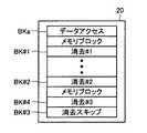
図23は、この発明の実施の形態4に従う半導体装置の全体の構成を概略的に示す図である。図23に示す半導体装置は、以下の点で、その構成が、図14に示す半導体装置と異なる。すなわち、メモリアレイ20が、複数のメモリブロックBK0−BKnに分割される。これらのメモリブロックBK0−BKnには共通に、ビット線BLが配設され、各メモリブロックの対応の列のメモリセルがビット線BLに接続される。[Embodiment 4]
FIG. 23 schematically shows an overall configuration of the semiconductor device according to the fourth embodiment of the present invention. The semiconductor device shown in FIG. 23 is different from the semiconductor device shown in FIG. 14 in the following points. That is, the
メモリブロックBK0−BKnには、それぞれ、行方向に沿って延在するアシストゲート線AGLおよびメモリゲート線MGLが配設される。また、メモリブロックBK0−BKnそれぞれに対して、ブロック埋込消去ゲート線BEGが配設される。メモリブロックBK0−BKnそれぞれにおいてローカル埋込消去ゲート線LEGが配設され、対応のブロック消去ゲート線BEGに結合される。ローカル埋込消去ゲート線LEGは、対応のメモリブロック内において各メモリセル列に沿って列方向に延在するように配置される。 In memory blocks BK0 to BKn, assist gate lines AGL and memory gate lines MGL extending along the row direction are provided, respectively. A block embedded erase gate line BEG is provided for each of the memory blocks BK0 to BKn. In each of memory blocks BK0 to BKn, a local buried erase gate line LEG is provided and coupled to a corresponding block erase gate line BEG. Local buried erase gate line LEG is arranged to extend in the column direction along each memory cell column in the corresponding memory block.
EG制御回路70は、消去モード時、メモリブロック単位で、ブロック埋込消去ゲート線BEGを選択状態へ駆動する。 In the erase mode, the
この図23に示す他の構成は、図14に示す半導体装置の構成と同じであり、対応する部分には同一参照番号を付し、その詳細説明は省略する。 The other configuration shown in FIG. 23 is the same as the configuration of the semiconductor device shown in FIG. 14. Corresponding portions are allotted with the same reference numerals, and detailed description thereof is omitted.
図24は、図23に示すメモリアレイ20の構成をより具体的に示す図である。図24に示す構成においては、消去単位が異なるメモリブロックが設けられているため、メモリブロックBK0−BKnの符号に代えて、符号BKAおよびBKBを用いる。 FIG. 24 is a diagram more specifically showing the configuration of
図24において、たとえば1Kバイトの容量のメモリブロックBKA0−BKA3と、例えば2Kバイトの容量のメモリブロックBKB0−BKB15が設けられる。メモリブロックBKA0−BKA3およびBKB0−BKB15に対しては、メモリブロック単位で消去が行なわれる。したがって、合計容量4KB(バイト)のメモリブロックBKA0−BKA3においては、消去単位は1Kバイトであり、一方、合計32KBのメモリブロックBKB0−BKB15においては、消去単位は2Kバイトである。この消去単位を異ならせることにより、アプリケーションに応じてデータを、消去単位の異なるメモリブロックに格納する。例えば、頻繁に書き換えるデータを容量の小さなメモリブロックBKA0−BKA3に格納し、データ量が多いまたは書換え頻度の小さなデータを容量の大きなメモリブロックBKB0−BKB15に格納する。 In FIG. 24, memory blocks BKA0 to BKA3 having a capacity of 1 Kbytes, for example, and memory blocks BKB0 to BKB15 having a capacity of 2 Kbytes, for example, are provided. Memory blocks BKA0-BKA3 and BKB0-BKB15 are erased in units of memory blocks. Therefore, in the memory blocks BKA0 to BKA3 having a total capacity of 4 KB (bytes), the erase unit is 1 Kbyte, while in the memory blocks BKB0 to BKB15 having a total capacity of 32 KB, the erase unit is 2 Kbytes. By changing the erase unit, data is stored in memory blocks having different erase units according to the application. For example, frequently rewritten data is stored in the memory blocks BKA0 to BKA3 having a small capacity, and data having a large amount of data or a small rewrite frequency is stored in the memory blocks BKB0 to BKB15 having a large capacity.
メモリブロックBKA0−BKA3およびBKB0−BKB15に共通にビット線BLが設けられる。図24においては、ビット線BL0およびBLkを代表的に示す。ビット線BL0−BLkに対し、各メモリブロックにおいてメモリセルMCの選択トランジスタ(アシストゲートトランジスタ)が結合される。この場合、データアクセスが各メモリブロックにおいて2ビット単位で実行されるため、記憶容量は、物理アドレスの1/2倍となる。 Bit lines BL are provided in common to memory blocks BKA0-BKA3 and BKB0-BKB15. FIG. 24 representatively shows bit lines BL0 and BLk. Select transistors (assist gate transistors) of memory cells MC are coupled to bit lines BL0-BLk in each memory block. In this case, since data access is executed in units of 2 bits in each memory block, the storage capacity is ½ times the physical address.
メモリブロックBKA0−BKA3およびBKB0−BKB15に共通に、列選択ゲート回路32が設けられる。この列選択ゲート回路32により選択されたビット線が、内部データバスを介してセンスアンプ回路48および書込ドライブ回路72に結合される。このセンスアンプ回路48および書込ドライブ回路72は、それぞれ、図23に示すセンスアンプ36およびデータ書込ドライバ38内に設けられる。 A column
メモリブロックBKA0−BKA3に対しては、ブロック埋込消去ゲート線BEGA0−BEGA3がそれぞれ設けられ、メモリブロックBKB0−BKB15には、ブロック埋込ゲート線BEGB0−BEGB15がそれぞれ設けられる。 Block embedded erase gate lines BEGA0-BEGA3 are provided for memory blocks BKA0-BKA3, respectively, and block embedded gate lines BEGB0-BEGB15 are provided for memory blocks BKB0-BKB15, respectively.
図25は、図24に示すメモリブロックにおける1つのメモリブロックに対する消去を行なう場合の、各ブロックのゲート配線の印加電圧を概略的に示す図である。図25において、消去対象のブロックにおいては、メモリセルMCeのローカル埋込消去ゲート線LEGに消去高電圧(10V)が印加される。メモリセルMCeのメモリゲートMGおよびアシストゲートAGは、オープン状態または0Vであり、ソース線SLは、接地ノードに結合される。したがって、消去時、アシストゲートAGを0Vに設定すれば、消去対象のメモリセルMCeのローカル埋込消去ゲート線LEGは、ビット線BLと分離される。 FIG. 25 schematically shows a voltage applied to the gate wiring of each block when erasing one memory block in the memory block shown in FIG. In FIG. 25, in the block to be erased, an erase high voltage (10 V) is applied to the local embedded erase gate line LEG of the memory cell MCe. Memory gate MG and assist gate AG of memory cell MCe are in the open state or 0 V, and source line SL is coupled to the ground node. Therefore, at the time of erasing, if assist gate AG is set to 0V, local embedded erase gate line LEG of memory cell MCe to be erased is separated from bit line BL.
この消去対象のメモリブロックと異なるメモリブロックにおいて、メモリセルMCdのローカル埋込消去ゲート線LEGは、0Vまたはオープン状態に維持される。メモリセルMCdのメモリゲートMGおよびアシストゲートAGには、消去対象のメモリセルMCeのメモリゲートMGおよびアシストゲートAGの印加電圧にかかわらず、別の電圧を印加することができる。したがって、ビット線BLに読出電圧または書込電圧を印加することができ、また、消去非対象のメモリブロックのソース線SLには書込電圧を印加することができ、応じて、メモリセルMCdに対してデータアクセス(読出/書込)を行なうことができる。すなわち、消去ブロックにおける消去電圧印加期間中に、並行して、別のメモリブロックに対してデータのアクセス(外部データの書込または読出)を行なうことができる。 In a memory block different from the memory block to be erased, the local embedded erase gate line LEG of the memory cell MCd is maintained at 0V or an open state. Different voltages can be applied to the memory gate MG and the assist gate AG of the memory cell MCd regardless of the voltages applied to the memory gate MG and the assist gate AG of the memory cell MCe to be erased. Therefore, a read voltage or a write voltage can be applied to the bit line BL, and a write voltage can be applied to the source line SL of the memory block not to be erased. Data access (read / write) can be performed. That is, data access (writing or reading of external data) can be performed on another memory block in parallel during the erase voltage application period in the erase block.
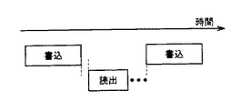
図26は、この発明の実施の形態4における消去およびデータアクセスシーケンスの一例を示す図である。図26において、消去対象ブロックにおいて消去電圧が印加される。この消去電圧印加と並行して、別のデータアクセスブロックにおいてデータの読出または書込を実行することができる。これにより、読出および書込の自由度が改善され、データアクセス効率が改善される。 FIG. 26 shows an example of an erase and data access sequence according to the fourth embodiment of the present invention. In FIG. 26, the erase voltage is applied to the block to be erased. In parallel with the application of the erase voltage, data reading or writing can be executed in another data access block. Thereby, the degree of freedom of reading and writing is improved, and the data access efficiency is improved.
消去モード時のベリファイ動作においては、単にデータアクセスブロックのデータアクセス完了時またはその間を縫って消去ベリファイ読出が実行されればよい。 In the verify operation in the erase mode, it is only necessary to execute the erase verify read when the data access of the data access block is completed or in between.
図27は、この発明の実施の形態4に従う半導体装置のデータアクセスシーケンスを示す図である。図27に示すアクセスシーケンスにおいては、書込および読出が交互に異なるメモリブロックに対して実行される。書込(プログラム)時においては、ビット線を用いて書込電圧が伝達されるため、書込および読出を並行して実行することはできない。 FIG. 27 shows a data access sequence of the semiconductor device according to the fourth embodiment of the present invention. In the access sequence shown in FIG. 27, writing and reading are alternately performed on different memory blocks. At the time of writing (programming), since the write voltage is transmitted using the bit line, writing and reading cannot be executed in parallel.
図28は、図23に示すコマンドレジスタ/制御回路24の構成を概略的に示す図である。この図28に示すコマンドレジスタ/制御回路24においては、指定された動作モードを特定するコマンドを格納するコマンドレジスタとして、消去コマンドレジスタ41e、書込コマンドレジスタ41w、および読出コマンドレジスタ41rが設けられる。これらのコマンドレジスタ41e、41wおよび41rは、図示しないコマンドデコーダからのデコード後のコマンドをそれぞれ格納する。 FIG. 28 schematically shows a structure of command register /
図28に示すコマンドレジスタ/制御回路20は、先の図18に示す構成と同様、消去制御部42、消去ベリファイ制御部43および消去ブロックアドレスレジスタ50を含む。消去制御部42は、消去コマンドレジスタ41eからの消去コマンドに従って消去モード指示ERSをアサートし、消去動作と並行してまたは消去完了後消去ベリファイ制御部43を活性化して消去ベリファイ動作を実行する。消去ベリファイが完了すると消去制御部42は、消去ベリファイ制御部43からの消去ベリファイ完了指示に従って消去動作を停止する。 The command register /
コマンドレジスタ/制御回路24においては、さらに、比較回路52A、読出制御部54A、書込制御部75および書込ベリファイ制御部77が設けられる。比較回路52Aは、書込コマンドレジスタ40wからの書込モード指示Cwriteおよび読出コマンドレジスタ41rからの読出モード指示Creadの一方のアサートと消去制御部42からの消去モード指示ERSのアサートに従って、消去ブロックアドレスレジスタ50に格納された消去ブロックアドレスと与えられたアドレス信号ADDのブロックアドレスとを比較する。比較結果が一致する場合、比較回路52Aは、データアクセス活性化信号ENAをネゲート状態に維持し、比較結果が不一致のときには、データアクセス活性化信号ENAをアサートする。 The command register /
読出制御部54Aは、書込制御部75からの書込モードイネーブル信号WRITEのネゲート(非活性化)時、読出モード指示Creadと比較回路52Aからのデータアクセス活性化指示とに従って、読出モードイネーブル信号READおよび読出動作活性化信号RENNを生成する。読出モードイネーブル信号READは、読出動作期間中イネーブル状態に設定され、読出動作活性化信号RENNは、実際のデータ読出を行なう期間を規定する。この半導体装置が、アドレス信号の変化に従って読出動作の活性化タイミングを設定する場合、特に、読出動作活性化信号RENNは生成されなくてもよい。また、読出動作活性化信号RENNに従ってアシストゲート線AGの活性化期間およびセンスアンプの活性化期間が規定される。 When the write mode enable signal WRITE from the
読出制御部54Aは、さらに、書込ベリファイ制御部77からの書込ベリファイ指示に従って読出モードイネーブル信号READおよび読出動作活性化信号RENNを活性化する。読出制御部54Aは、また、図示しない経路により、消去ベリファイ制御部43からの消去ベリファイ指示に従って読出モードイネーブル信号READおよび読出動作活性化信号RENNを活性化する。 Read
書込制御部75は、比較回路52Aからのデータアクセス活性化信号ENAのアサート時に書込モード指示Cwriteがアサートされると、書込モードイネーブル信号WRITEおよび書込動作活性化信号WRENを活性化する。書込動作モード指示信号WRITEは書込動作期間を規定し、書込動作活性化信号WRENは、メモリゲートおよびビット線に印加される書込電圧の印加期間を規定する。書込制御部75は、書込完了後、書込ベリファイ制御部77を起動し、書込ベリファイを実行する。 Write
書込制御部75は、読出制御部54Aが読出モードイネーブル信号READをアサートしているときには、非活性状態に維持される。 Write
この発明の実施の形態4に従う半導体装置における行デコーダの構成としては、各メモリブロックに対して、図19に示す構成がローカルデコーダとして設けられればよい。 As the configuration of the row decoder in the semiconductor device according to the fourth embodiment of the present invention, the configuration shown in FIG. 19 may be provided as a local decoder for each memory block.
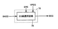
図29は、図23に示すEG制御回路70の構成の一例を概略的に示す図である。図29に示すEG制御回路70においては、EG線選択回路79が設けられる。EG線選択回路79は、消去モード指示ERSのアサート時、アドレス信号ADDに含まれるブロックアドレスBADDをデコードし、選択メモリブロックに対するブロック埋込消去ゲート線BEGに消去高電圧VPEGを伝達する。残りの非選択メモリブロックに対しては、EG線選択回路79は、ブロック埋込消去ゲート線を接地電圧に維持する(またはオープン状態に維持する)。 FIG. 29 schematically shows an example of a configuration of
各動作モードに必要な電圧については、消去制御部42、書込制御部75および読出制御部54Aからの消去モード指示ERS、書込モードイネーブル信号WRITEおよび読出モードイネーブル信号READに従って、それぞれ図23に示す電圧発生回路において消去電圧、書込電圧、読出電圧および消去/書込ベリファイ読出電圧が生成され(または選択され)、行デコーダおよび列デコーダへ与えられ、各動作モードに応じた電圧が選択メモリセルへ供給される。 The voltages necessary for each operation mode are shown in FIG. 23 in accordance with erase mode instruction ERS, write mode enable signal WRITE, and read mode enable signal READ from erase
以上のように、この発明の実施の形態4に従えば、消去動作と並行して別のメモリブロックにおいて読出または書込を実行可能としている。応じて、データアクセス効率がさらに改善される。また実施の形態1および2と同様の効果を得ることができる。 As described above, according to the fourth embodiment of the present invention, reading or writing can be executed in another memory block in parallel with the erase operation. Accordingly, the data access efficiency is further improved. Further, the same effect as in the first and second embodiments can be obtained.
なお、この実施の形態4においても、実施の形態3と同様、書込または読出を行なう期間および間隔は、消去電圧印加期間よりも十分短くされ、消去動作に悪影響を及ぼさないようにされる。 In the fourth embodiment, as in the third embodiment, the period and interval for writing or reading are made sufficiently shorter than the erasing voltage application period so that the erasing operation is not adversely affected.
[実施の形態5]
図30は、この発明の実施の形態5に従う半導体装置の全体の構成を概略的に示す図である。この図30に示す半導体装置は、以下の点で、図23に示す半導体装置とその構成が異なる。すなわち、コマンドレジスタ/制御回路24Aは、消去動作時には、外部に消去ステータス信号RYIBY_ERを出力し、かつ内部でデータ読出、書込またはベリファイ動作実行中、アクセス禁止ステータス信号RYIBY_RWを外部装置へ出力する。[Embodiment 5]
FIG. 30 schematically shows a whole structure of the semiconductor device according to the fifth embodiment of the present invention. The semiconductor device shown in FIG. 30 differs from the semiconductor device shown in FIG. 23 in the following points. That is, command register /
また、ベリファイカウンタ80およびマルチプレクサ82が設けられる。ベリファイカウンタ80は、消去ベリファイ時および書込ベリファイ時、カウント動作によりベリファイ対象のメモリセルを特定するアドレスを生成する。マルチプレクサ82は、アドレスレジスタ22からの内部アドレスとベリファイカウンタ80からのベリファイアドレスの一方を選択して内部アドレスを生成して、列デコーダ30、行デコーダ28およびEG制御回路70へ与える。マルチプレクサ80からの内部アドレスは、またデータ書込ドライバ38およびセンスアンプ36へも与えられる。 Also, a verify
この図30に示す半導体装置の他の構成は、図23に示す半導体装置の構成と同じであり、対応する部分には同一参照番号を付し、その詳細説明は省略する。 Other structures of the semiconductor device shown in FIG. 30 are the same as those of the semiconductor device shown in FIG. 23, and corresponding portions are denoted by the same reference numerals, and detailed description thereof is omitted.
図30に示す半導体装置においては、コマンドレジスタ/制御回路24Aは、内部でデータの読出、書込(実際の書込動作)またはベリファイ動作を行なわれたとき、アクセス禁止ステータス信号RYIBY_RWをアサートする。したがって、アクセス禁止ステータス信号RYIBY_RWがアサート状態のときには、処理装置などの外部装置は、この半導体装置へのアクセスが禁止される。 In the semiconductor device shown in FIG. 30, command register /
一方、コマンドレジスタ/制御回路24Aからの消去ステータス信号RYIBY_ERがアサート状態のときには、この半導体装置内部で消去動作が行なわれるときである(消去ベリファイ動作は行なわれていない)。したがって、この場合には、外部からのデータのアクセス(書込/読出)を許可する。内部で、ベリファイ動作が行なわれるとき、外部アクセスを禁止することによって、データの衝突を確実に防止して、高速のデータアクセスを実現することができる。 On the other hand, when the erase status signal RYIBY_ER from the command register /
図31は、消去時の動作シーケンスの一例を示す図である。図31に示すように、メモリアレイ20における1つのメモリブロックに対する消去が行なわれる。この消去が、内部で行なわれると、コマンドレジスタ/制御回路24Aが、消去ステータス信号RYIBY_ERをアサートする。この信号RYIBY_ERのアサートにより、外部装置は、アクセス不可能であることを報知される。 FIG. 31 is a diagram showing an example of an operation sequence at the time of erasing. As shown in FIG. 31, erasure is performed on one memory block in
外部装置が、この状態で、読出アクセス(リードアクセス)を行なうと、データアクセス禁止ステータス信号RYIBY_RWがアサートされる。1つのリード動作が内部で完了すると、この信号RYIBY_RWがデアサート(ネゲート)される。信号RYIBY_RWのネゲートに従って次の読出動作が繰返し実行される。 When the external device performs read access (read access) in this state, data access prohibition status signal RYIBY_RW is asserted. When one read operation is completed internally, this signal RYIBY_RW is deasserted (negated). The next read operation is repeatedly executed according to the negation of the signal RYIBY_RW.
メモリブロックに対する消去および消去ベリファイが完了すると、消去ステータス信号RYIBY_ERがネゲートされる。このとき、消去ベリファイ動作が実行中は(ベリファイ動作は、記号VRで示す)、信号RYIBY_ERはアサート状態であり、さらに、信号RYIBY_RWがアサートされる。応じて、消去ベリファイ動作期間中、外部からのアクセスは禁止される。このベリファイ動作が完了し、再び消去電圧の印加が行なわれると、信号RYIBY_ERがアサートされ、外部装置に対してアクセス可能が報知される。 When the erase and erase verify for the memory block is completed, the erase status signal RYIBY_ER is negated. At this time, while the erase verify operation is being executed (the verify operation is indicated by the symbol VR), the signal RYIBY_ER is in the asserted state, and the signal RYIBY_RW is asserted. Accordingly, external access is prohibited during the erase verify operation period. When the verify operation is completed and the erase voltage is applied again, the signal RYIBY_ER is asserted to notify the external device that access is possible.
消去ベリファイ動作完了に従って、信号RYIBY_RWはネゲートされる。したがって、消去電圧印加期間中に、読出動作が繰返し実行されると、内部の読出動作が完了するごとに、信号RYIBY_RWがネゲート状態となり、内部で読出動作が行なわれるときにアサート状態とされ、内部でデータ読出が行なわれるとき外部からのアクセスは禁止される。読出動作が完了すると、信号RYIBY_RWはネゲートされる。消去が完了すると、また、信号RYIBY_ERがネゲートされる。 The signal RYIBY_RW is negated in accordance with the completion of the erase verify operation. Therefore, when the read operation is repeatedly executed during the erase voltage application period, every time the internal read operation is completed, the signal RYIBY_RW is negated and is asserted when the internal read operation is performed. When data reading is performed, external access is prohibited. When the read operation is completed, the signal RYIBY_RW is negated. When the erasing is completed, the signal RYIBY_ER is negated again.
消去電圧(パルス)印加時に、信号RYIBY_ERを用いて、外部にデータアクセス可能を報知し、また、内部で読出動作が行なわれていることを外部へ信号RYIBY_RWを用いて報知することにより、消去動作時に並行して確実に外部からデータ読出アクセスを、アクセスデータとベリファイデータとの衝突を回避しつつ、行なうことができる。 When the erase voltage (pulse) is applied, the signal RYIBY_ER is used to notify the outside that data access is possible, and the internal read operation is performed to the outside using the signal RYIBY_RW, thereby erasing operation. In some cases, it is possible to reliably perform data read access from the outside while avoiding a collision between the access data and the verify data.
図32は、この消去パルス印加時の他の動作シーケンスの例を示す図である。図32においては、消去パルス印加と並行して書込動作(ライト動作)が行なわれる。このライト動作時においては、書込ベリファイが実行される。 FIG. 32 is a diagram showing an example of another operation sequence when the erase pulse is applied. In FIG. 32, a write operation (write operation) is performed in parallel with the application of the erase pulse. During this write operation, write verify is executed.
消去パルスが印加されると、信号RYIBY_ERがアサートされ、外部に対しデータアクセス可能が報知される。応じて、外部からデータの書込アクセスが実行され、信号RYIBY_RWがアサートされる。書込動作が完了すると、書込ベリファイ動作が続いて実行される。書込ベリファイ動作(VR動作)が実行されるため、信号RYIBY_RWは、継続してアサート状態に維持される。書込ベリファイ動作が完了すると、1つのデータ書込が完了し、信号RYIBY_RWがネゲートされる。 When the erase pulse is applied, the signal RYIBY_ER is asserted to notify the outside that data access is possible. In response, a data write access is executed from the outside, and signal RYIBY_RW is asserted. When the write operation is completed, the write verify operation is subsequently executed. Since the write verify operation (VR operation) is performed, the signal RYIBY_RW is continuously maintained in the asserted state. When the write verify operation is completed, one data write is completed and the signal RYIBY_RW is negated.
消去動作時、信号RYIBY_RWのネゲートに従って、次の外部からの書込アクセスが実行される。データ書込およびベリファイ動作が完了すると、信号RYIBY_RWがネゲートされる。この信号RYIBY_RWのネゲートに従って、消去動作が完了し、信号RYIBY_ERがネゲートされる。この消去パルス印加後、消去ベリファイ動作が、消去対象のメモリセルが確実に消去されたかを識別するために実行される。このとき、信号RYIBY_ERはアサートされるものの、信号RYIBY_RWがアサート状態であり、外部からの書込アクセスは禁止される。信号RYIBY_ERおよびRYIBY_RWを内部で利用することにより、書込ベリファイと消去ベリファイトの競合を回避することができる。 During the erase operation, the next external write access is executed in accordance with the negation of the signal RYIBY_RW. When the data write and verify operations are completed, signal RYIBY_RW is negated. According to the negation of the signal RYIBY_RW, the erase operation is completed, and the signal RYIBY_ER is negated. After the erase pulse is applied, an erase verify operation is performed to identify whether or not the memory cell to be erased has been erased reliably. At this time, although the signal RYIBY_ER is asserted, the signal RYIBY_RW is in the asserted state, and external write access is prohibited. By using signals RYIBY_ER and RYIBY_RW internally, it is possible to avoid contention between write verify and erase verify.
消去ベリファイ動作により消去動作が完了すると、消去ステータス信号RYIBY_ERがネゲートされる。一方、消去ベリファイ動作により消去フェイルと判定されると、消去ステータス信号RYIBY_ERが引続きアサートされ、消去パルス印加が引続き実行される。このとき、消去ベリファイ動作完了に従って信号RYIBY_RWがネゲートされ、外部からの書込アクセスが許可される。 When the erase operation is completed by the erase verify operation, the erase status signal RYIBY_ER is negated. On the other hand, if the erase verify operation determines that an erase failure has occurred, the erase status signal RYIBY_ER is continuously asserted, and the erase pulse application is continued. At this time, the signal RYIBY_RW is negated in accordance with the completion of the erase verify operation, and external write access is permitted.
内部で書込動作が開始されると、信号RYIBY_RWがアサートされ、データ書込が実行され、続いて、書込ベリファイが実行される。この書込および書込ベリファイが完了すると、信号RYIBY_RWがネゲートされる。また、消去パルス印加期間が完了すると、信号RYIBY_ERがネゲートされる。消去ベリファイ動作が実行されるため、再び信号RYIBY_RWがアサートされ、外部からの書込アクセスは禁止される。 When the write operation is started internally, the signal RYIBY_RW is asserted, data write is executed, and then write verify is executed. When this writing and write verification are completed, signal RYIBY_RW is negated. When the erase pulse application period is completed, the signal RYIBY_ER is negated. Since the erase verify operation is executed, the signal RYIBY_RW is asserted again, and external write access is prohibited.
以上のように、内部で消去ベリファイまたは書込ベリファイを実行する場合、外部アクセスを禁止することにより、ベリファイ動作と外部からのデータアクセス動作が衝突するのを回避して消去動作に並行して外部からのデータアクセス(書込/読出)を実行することができる。特に、消去ステータス信号RYIBY_ERを、消去時の消去パルス印加時および消去ベリファイ動作中はアサート状態に維持し、アクセスステータス信号RYIBY_RWは、メモリセルへのアクセス時、すなわち、消去ベリファイ動作時、外部書込アクセス時および外部読出アクセス時にアサート状態に設定する。これにより、信号RYIBY_ERおよびRYIBY_RWを互いに独立に制御することができ、制御が容易となる。 As described above, when executing erase verify or write verify internally, by prohibiting external access, it is possible to avoid collision between the verify operation and the external data access operation in parallel with the erase operation. Data access (write / read) from can be performed. In particular, the erase status signal RYIBY_ER is maintained in an asserted state when an erase pulse is applied during erase and during an erase verify operation, and the access status signal RYIBY_RW is externally written when accessing a memory cell, that is, during an erase verify operation. Set to assert state during access and external read access. Thereby, the signals RYIBY_ER and RYIBY_RW can be controlled independently of each other, and the control becomes easy.
なお、図31および図32に示す構成において、各データ読出または書込ごとに、読出コマンドまたは書込コマンドが与えられるように動作を示している。しかしながら、この読出コマンドおよび書込コマンドとしてバーストアクセスモードが指定され、連続的にデータの読出または書込が実行されてもよい。この場合、信号RYIBY_RWは、このバーストアクセス期間中アサート状態に維持される。 In the configuration shown in FIGS. 31 and 32, the operation is shown such that a read command or a write command is given for each data read or write. However, burst access mode may be designated as the read command and write command, and data reading or writing may be executed continuously. In this case, the signal RYIBY_RW is maintained in the asserted state during this burst access period.
図33は、図30に示すコマンドレジスタ/制御回路24Aの構成を概略的に示す図である。この図33に示すコマンドレジスタ/制御回路24Aの構成は、以下の点で、図28に示すコマンドレジスタ/制御回路24の構成と異なる。すなわち、書込ベリファイ制御部77Aが、書込ベリファイ指示信号WVRを生成し、消去ベリファイ制御部43Aが、消去ベリファイ指示信号EVRを生成する。この信号WVRおよびEVRのアサート時、ベリファイ動作が実行される。 FIG. 33 schematically shows a structure of command register /
消去制御部42は、消去電圧印加期間中および消去ベリファイ動作期間中、信号RYIBY_ERをアサートして外部へ出力する。これらの信号WVR、EVR、読出モードイネーブル信号READおよび書込モードイネーブル信号WRITEを受ける信号発生器84が、信号RYIBY_RWを生成するために設けられる。この信号発生器84は、与えられた信号WVR、READ、EVRおよびWRITEのいずれかのアサート時、信号RYIBY_RWをアサートして外部へ出力する。これにより、内部でデータの書込、読出およびベリファイが実行されている場合、信号RYIBY_RWをアサートすることができる。 The erase
なお、信号発生器84に対し、信号READおよびWRITEに代えて活性化信号WRENおよびRENNが与えられてもよい。 It is noted that activation signals WREN and RENN may be applied to signal
消去ベリファイ制御部43Aは、消去制御部42と同様、シーケンスコントローラで構成され、消去パルス印加後、所定のシーケンスで消去ベリファイ動作を実行する。これによりに、信号RYIBY_RWを利用することにより、このベリファイ動作と外部からのデータ読出アクセスとが衝突するのを防止することができる。 Similarly to the erase
以上のように、この発明の実施の形態5に従えば、内部消去状態を示す信号と内部の読出、書込およびベリファイ動作を示す信号とを外部の装置に出力している。したがって、内部でのベリファイ動作時に、外部からの書込および読出アクセスを禁止することにより、データの外部アクセスとベリファイ動作が競合するのを防止することができる。応じて、正確かつ効率的に、消去パルス印加時においても、データアクセスを行なうことができる。 As described above, according to the fifth embodiment of the present invention, the signal indicating the internal erase state and the signal indicating the internal read, write and verify operations are output to the external device. Therefore, by prohibiting external write and read access during the internal verify operation, it is possible to prevent the external access of data and the verify operation from competing. Accordingly, data access can be performed accurately and efficiently even when an erase pulse is applied.
本実施の形態5においては、消去電圧(パルス)印加期間中の消去ベリファイは行なわれていない。この消去パルス印加中の消去ベリファイは、以下の実施の形態において説明するように、外部アクセスとの間でタイミング調整が行われて実行されてもよい。 In the fifth embodiment, erase verify is not performed during the erase voltage (pulse) application period. The erase verify during the application of the erase pulse may be executed by adjusting the timing with the external access as described in the following embodiments.
[実施の形態6]
図34は、この発明の実施の形態6に従う半導体装置の消去時のデータアクセスシーケンスの一例を示す図である。図34に示す動作シーケンスにおいて、消去ベリファイ動作中に、読出アクセス要求が発行されたとき、消去ベリファイ動作VRを停止させ、要求された読出動作を実行する。データ読出アクセス完了後、停止した消去ベリファイ動作を残りのベリファイアドレス領域VAについて実行する。[Embodiment 6]
FIG. 34 shows an example of a data access sequence at the time of erasure of the semiconductor device according to the sixth embodiment of the present invention. In the operation sequence shown in FIG. 34, when a read access request is issued during the erase verify operation, the erase verify operation VR is stopped and the requested read operation is executed. After the completion of the data read access, the stopped erase verify operation is executed for the remaining verify address area VA.
これにより、読出データアクセス時、待ち時間を生じさせることなく、データ読出アクセスを実行することができる。 As a result, the data read access can be executed without causing a waiting time when the read data is accessed.
図35は、この発明の実施の形態6に従う半導体装置のコマンドレジスタ/制御回路の構成を概略的に示す図である。半導体装置の全体の構成は、図23に示す半導体装置の構成と同じである。 FIG. 35 schematically shows a structure of a command register / control circuit of the semiconductor device according to the sixth embodiment of the present invention. The entire configuration of the semiconductor device is the same as that of the semiconductor device shown in FIG.
図35に示すコマンドレジスタ/制御回路24Aは、以下の点で、その構成が図33に示すコマンドレジスタ/制御回路24Aと異なる。すなわち、信号発生器84は、設けられない。すなわち、内部ステータスを外部に報知する信号は、本実施の形態6においては利用されない。消去ベリファイ制御部43Bは、読出制御部54Aからの読出モードイネーブル信号READを受け、この読出モードイネーブル信号READがアサートされると、実行中のベリファイ動作を停止させ、読出制御回路54Aに対して外部読出アクセス許可を報知する。また、カウント更新指示信号VRCNTをネゲートしてベリファイカウンタ80のカウント動作を停止させる。 The command register /
読出制御回路54Aは、消去ブロックと異なるメモリブロックへの読出アクセス時、この消去ベリファイ制御部43Bからの読出アクセス許可を受けると、読出動作活性化信号RENNをアサートしてデータの外部読出動作を実行する。読出アクセスが完了すると、読出制御部54Aは、読出モードイネーブル信号READをネゲートする。この読出モードイネーブル信号READのネゲートに従って、カウント更新指示信号VRCNTをアサートして消去ベリファイを停止したベリファイアドレスから再開する。 When the
また、この消去ベリファイ制御部43Bは、消去制御部42から、消去ベリファイ開始指示が与えられた時に、読出モードイネーブル信号READがアサートされ、外部読出アクセスが実行されている場合には、この消去ベリファイを外部データ読出アクセスが完了するのを待つ。消去ベリファイ制御部43Bは、この読出モードイネーブル信号READがネゲートされると、ベリファイカウンタ80へカウント更新信号VRCNTを与え、このベリファイカウンタ80からのベリファイアドレスカウントをマルチプレクサ82に選択させて、このベリファイカウンタ80からのカウント値に従って消去ベリファイ動作を実行する。 The erase verify
この図35に示すコマンドレジスタ/制御回路24Aの他の構成は、図33に示すコマンドレジスタ/制御回路24Aの構成と同様であり、その詳細説明は省略する。 The other configuration of the command register /
以上のように、この発明の実施の形態6に従えば、消去時にベリファイ動作実行時外部からの読出アクセス要求が与えられたとき、または、その逆に外部読出アクセス中に消去ベリファイ指示がアサートされると、消去ベリファイ動作を停止または待ち合わせ、外部からの読出アクセスを実行している。外部読出アクセスに対して消去ベリファイ動作よりも高い優先順位を与えている。これにより、外部からの読出アクセスの待ち時間を短縮することができ、高速のデータ読出を行なうことができる。 As described above, according to the sixth embodiment of the present invention, the erase verify instruction is asserted when an external read access request is given at the time of executing the verify operation at the time of erasing, or vice versa. Then, the erase verify operation is stopped or waited, and external read access is executed. A higher priority is given to the external read access than to the erase verify operation. As a result, the waiting time for external read access can be reduced, and high-speed data reading can be performed.
[実施の形態7]
図36は、この発明の実施の形態7に従う半導体装置の全体の構成を概略的に示す図である。図36に示す半導体装置は、図30に示す半導体装置と以下の点で、その構成が異なる。すなわち、消去ブロックを特定する消去アドレスを複数個格納する消去アドレスレジスタファイル90が設けられる。消去アドレスレジスタファイル90は、コマンドレジスタ/制御回路24Bの制御の基に、格納した消去アドレスを順次読出し、その消去ブロックアドレスEADをEG制御回路70へ与える。この図36に示す半導体装置の他の構成は、図30に示す半導体装置の構成と同じであり、対応する部分には同一参照番号を付し、その詳細説明は省略する。[Embodiment 7]
FIG. 36 schematically shows a whole structure of the semiconductor device according to the seventh embodiment of the present invention. The semiconductor device shown in FIG. 36 differs from the semiconductor device shown in FIG. 30 in the following points. That is, an erase
図37は、図36に示す消去アドレスレジスタファイル90の構成の一例を概略的に示す図である。消去アドレスレジスタファイル90は、複数のレジスタを含み、各レジスタが、それぞれ消去アドレス格納領域90aおよび有効フラグ格納領域90bを含む。レジスタREG0−REGaは、シフト動作により、その記憶データを順次。FIFO8ファーストイン・ファーストアウト)態様で読出す。 FIG. 37 schematically shows an example of the structure of erase
有効フラグ格納領域90bに格納されるフラグFG(FG0−FGj)が有効状態を示すとき、この対応の消去アドレス格納領域90aに含まれる消去アドレスEAD(EAD0−EADj)が消去ブロックを指定するアドレスとしてEG制御回路70へ与えられ、指定された消去ブロックに対する消去が実行される。 When the flag FG (FG0-FGj) stored in the valid
図38は、この発明の実施の形態7におけるメモリアレイ内のメモリブロックの消去シーケンスを概略的に示す図である。メモリアレイ(メモリマット)20において、複数のメモリブロックが設けられる。ここで、メモリマットは、行デコーダおよび列選択ゲート回路により囲まれるメモリアレイの部分であり、単一のバンクを構成する部分を示す。 FIG. 38 schematically shows an erase sequence of memory blocks in the memory array according to the seventh embodiment of the present invention. In the memory array (memory mat) 20, a plurality of memory blocks are provided. Here, the memory mat is a portion of the memory array surrounded by the row decoder and the column selection gate circuit, and indicates a portion constituting a single bank.
図38において、メモリブロックBKaに対してデータアクセスが行なわれるとき、消去アドレスレジスタファイル90において、ブロック♯1、BK♯2、BK♯4を特定する消去アドレスが順次格納され、メモリブロックBK♯3に対しては、消去非実行を示すスキップフラグ(リセット状態とされた有効フラグ)が格納される。この場合、メモリブロックBKaに対するデータアクセス(読出または書込)と並行して、メモリブロックBK♯1、BK♯2に対する消去が行なわれ、メモリブロックBK♯3に対しては消去はスキップされて実行されない。メモリブロックBK♯3に対して割当てられた消去時間の経過後、メモリブロックBK♯4に対する消去が実行される。 In FIG. 38, when data access is performed to memory block BKa, erase addresses specifying
スキップアドレスを消去アドレスレジスタファイルにおいて格納することにより、データアクセスのバックグラウンドで消去を行なう期間を停止させる。この消去アドレスおよびスキップアドレスは、外部からのコマンドにより指定される。 By storing the skip address in the erase address register file, the erase period is stopped in the background of data access. The erase address and skip address are designated by an external command.
電源遮断時においては、消去アドレスレジスタファイル90に格納された未実行の消去アドレスが、メモリアレイ20の特定の領域に格納される。 When the power is shut off, an unexecuted erase address stored in the erase
図39は、この発明の実施の形態7における消去およびデータアクセス動作シーケンスを概略的に示す図である。すなわち、メモリアレイの図38に示すメモリブロックBKaに対するデータアクセスを実行中、メモリブロックBK♯1に対する消去(♯1)が実行される。消去ベリファイ動作時には、外部からの読出アクセスは禁止される。このベリファイ動作が完了し、メモリブロックBK♯1の消去が完了すると、次のメモリブロックBK♯2に対する消去(♯2)が実行される。メモリブロックBK♯3が特定されるとき、そのメモリブロックは消去スキップブロックであり、消去は実行されない。この間を消去停止期間とし、所定期間経過後(消去が必要な期間)、次のメモリブロックBK♯4に対する消去(♯3)が実行される。 FIG. 39 schematically shows an erase and data access operation sequence in the seventh embodiment of the invention. That is, erasure (# 1) is performed on memory
したがって、この外部からのデータアクセス(データ読出時)時、外部に対してほぼ消去動作を見えなくすることができ、アクセス効率を改善することができる。 Therefore, at the time of data access from the outside (during data reading), the erase operation can be made almost invisible to the outside, and the access efficiency can be improved.
図40は、図36に示すコマンドレジスタ/制御回路24Bの構成を概略的に示す図である。図40に示すコマンドレジスタ/制御回路24Bは、以下の点で、図33に示すコマンドレジスタ/制御回路24Aの構成とその構成が異なる。すなわち、図40において、比較回路52Aからのデータアクセス活性化信号ENAが、消去制御部42へ与えられる。消去アドレスレジスタファイル90に対するアドレスおよびフラグの書込が、消去制御部42の制御の下に行なわれる。消去制御部42は、消去/スキップコマンドレジスタ41eeからのコマンドに従って消去に必要な動作を制御する。 FIG. 40 schematically shows a structure of command register /
消去アドレスレジスタファイル90に対し、電源遮断検出制御部94と消去アドレスロード/セーブ制御部96が設けられる。電源遮断検出制御部94は、外部からの電源VDDの遮断時に、消去アドレスロード/セーブ制御部96に電源遮断検出信号を与える。消去アドレスロード/セーブ制御部96は、電源遮断検出信号のアサート時、セーブ書込イネーブル信号SWENをアサートして書込制御部75へ与え、電源回復時、ロード読出イネーブル信号LRENをアサートして読出制御部54Bへ与える。すなわち、消去アドレスロード/セーブ制御部96は、電源遮断および回復時の消去アドレスレジスタファイル90に対するデータの書込および読出を制御する。 For the erasure
書込制御部75Aは、書込モード指示Cwriteのアサート時の動作制御に加えて、セーブ書込イネーブル信号SWENのアサート時、書込モードイネーブル信号WRITEおよび書込動作活性化信号WRENをアサートし、消去アドレスレジスタファイル90に格納される消去アドレスおよびフラグのメモリアレイの所定のメモリ領域への書込動作を制御する。 The
読出制御部54Bは、ロード読出イネーブル信号LRENのアサート時、また読出モードイネーブル信号READおよび読出活性化信号RENNをアサートし、このロードされた消去アドレスおよびフラグのメモリアレイの所定の領域からの読出動作を制御する。この読出されたロード消去アドレスおよびフラグは、消去アドレスロード/セーブ制御部96により、消去アドレスレジスタファイル90に順次格納される。 The
なお、図40において、信号発生器84は設けられず、また、信号RYIBY_ERは発生されなくてもよい。消去は、外部データアクセスのバックグランドで実行されるため、外部装置に対して消去パルス印加期間を報知することは特に要求されないためである。消去コマンドとして、通常の消去モードとバックグランドで消去を行なうバックグランド消去モードが準備されている場合には、信号RYIBY_ERが利用されてもよい。 In FIG. 40, the
この図42に示すコマンドレジスタ/制御回路24Bの他の構成は、図33に示すコマンドレジスタ/制御回路24Aの構成と同じであり、対応する部分には同一参照番号を付し、その詳細説明は省略する。 The other configuration of the command register /
図41は、図40に示すコマンドレジスタ/制御回路24Bの消去アドレスレジスタファイル90への格納動作を示すフロー図である。以下、図41を参照して、図40に示すコマンドレジスタ/制御回路24Bの消去レジスタファイル格納動作について説明する。 FIG. 41 is a flowchart showing the storing operation to the erase
まず、コマンドレジスタ/制御回路24Bは、外部からコマンドが印加されるのを待つ(ステップST1)。外部からのコマンドが印加されると、消去制御部42は、この消去/スキップコマンドレジスタ41eeに格納されたコマンドが消去コマンドであるか(ステップST2)またはスキップコマンドであるか(ST4)を判別する。 First, the command register /
与えられたコマンドが消去コマンドの場合(ステップST2)、消去制御部42は、与えられた消去アドレスを消去アドレスレジスタファイル90に格納するとともに、対応のレジスタの有効フラグFLGをセットする。消去アドレスレジスタへのアドレス格納およびフラグセット後、レジスタファイル90のレジスタのシフト動作を実行する(ステップST3)。 When the given command is an erase command (step ST2), the erase
一方、与えられたコマンドがスキップコマンドの場合(ステップST4)、消去制御部42は、レジスタファイル90にスキップアドレスを格納し、対応の有効フラグをリセット状態に維持する。この後、レジスタファイルのレジスタを1段シフトする。これにより、消去アドレスおよびスキップアドレス格納が完了する。このとき、単にスキップフラグのみが格納されてもよい(有効フラグをリセット状態に維持する)。次いで、レジスタを1段シフトする。 On the other hand, when the given command is a skip command (step ST4), the
与えられたコマンドが消去コマンド(バックグラウンド消去コマンドでもなく、また消去スキップコマンドでもない場合には(ステップST2およびST4において判定結果がNOのとき)、このコマンドが指定する動作の実行を、書込コマンドレジスタ41wまたは読出コマンドレジスタ41rに格納される動作モード指示CwriteおよびCreadのいずれかに従って、書込制御部75Aまたは読出制御部54Bにより、指定された動作の実行が制御される。 If the given command is not an erase command (not a background erase command or an erase skip command (when the determination result is NO in steps ST2 and ST4), execution of the operation designated by this command is performed. Execution of the designated operation is controlled by the
消去アドレスレジスタファイル90がシフトレジスタで構成される場合、最終段のレジスタから先頭消去アドレスを読出すには、レジスタファイルのレジスタ段数コマンドが印加される必要がある。しかしながら、消去アドレスレジスタファイル90が、書込アドレスおよび読出アドレスに従ってFIFO態様でデータの書込および読出を行なう構成の場合、最初に1回格納された消去アドレスに従って消去を実行することができる。 When the erase
なお、消去コマンドとしては、外部から消去のみが指定されて通常の消去動作を行なうモードを指定する通常消去コマンドと、外部からのデータアクセスと並行してバックグラウンドモードで消去を行なうバックグラウンド消去モードを指定するコマンドがそれぞれ別々に設けられており、バックグラウンド消去コマンドが印加されたときに、消去アドレスレジスタファイル90への消去アドレスの格納動作が実行されるように構成されてもよい。 As an erase command, a normal erase command that designates a mode in which only an external erase is designated and a normal erase operation is performed, and a background erase mode that performs erase in the background mode in parallel with external data access May be separately provided, and an operation of storing an erase address in the erase
図42は、図40に示すコマンドレジスタ/制御回路24Bのバックグラウンド消去モード時の動作を示すフロー図である。以下、図42を参照して、図40に示すコマンドレジスタ/制御回路24Bのバックグラウンド消去動作について説明する。 FIG. 42 is a flowchart showing the operation of the command register /
消去制御部42は、消去アドレスレジスタファイル90から、最も古く格納されたレジスタの内容をレジスタのシフト動作により読出す(ステップST10)。このレジスタファイルから与えられたレジスタの内容に対して有効フラグがセット状態であるかリセット状態であるかの判定が行なわれる(ステップST11)。 The erase
有効フラグがセット状態でなく、リセット状態の場合には、消去アドレスが指定するメモリブロックに対する消去は実行されない。所定期間の待機の後(ステップST12)、再びステップST10に戻る。一方、有効フラグがセット状態の場合には、対応の消去アドレスが指定するメモリブロックに対する消去を実行する必要がある。このときには、先ず、比較回路52Aにおいて消去アドレスが示す消去対象ブロックとデータアクセスが行なわれているメモリブロックが同じであるかの判定が行なわれる(ステップST13)。消去対象メモリブロックとデータアクセスメモリブロックとが同一の場合、この消去対象のメモリブロックに対する消去を行なうことができないため(アクセス対象のデータが変更されるため)、データアクセス(読出または書込)が完了するのを待つ(ステップST14)。このデータアクセス完了後、再びステップST13に戻る。 When the valid flag is not in the set state but is in the reset state, the memory block specified by the erase address is not erased. After waiting for a predetermined period (step ST12), the process returns to step ST10 again. On the other hand, when the valid flag is in the set state, it is necessary to execute erasure on the memory block designated by the corresponding erase address. At this time, first, in
一方、消去メモリブロックとデータアクセスメモリブロックとが異なるメモリブロックの場合には、その消去アドレスが指定するメモリブロックに対する消去を実行する(ステップST15)。 On the other hand, if the erase memory block and the data access memory block are different memory blocks, the memory block specified by the erase address is erased (step ST15).
この消去が完了すると(ステップST16)、再び、ステップST10に戻り、消去アドレスレジスタファイル90からのレジスタの内容のシフトアウト読出以降の動作を実行する。これにより、データアクセスのバックグラウンドでデータアクセスメモリブロックと異なるメモリブロックに対する消去を実行することができる。 When this erasure is completed (step ST16), the process returns to step ST10 again, and the operations after the shift-out reading of the register contents from the erase
また、スキップアドレスが指定するメモリブロックに対しては、有効フラグがリセット状態のとき、所定期間待機することにより、このスキップアドレスが指定するメモリブロックに対する消去期間消去を実行する必要がなく、不必要な消去を停止させて消費電流を低減する。 Also, for the memory block specified by the skip address, when the valid flag is in the reset state, it is not necessary to wait for a predetermined period, thereby eliminating the erase period erase for the memory block specified by the skip address. Erasing is stopped to reduce current consumption.
なお、この図40に示すコマンドレジスタ/制御回路24Bの構成においては、消去ベリファイ動作(VR動作)においては、外部からのデータアクセスを停止させている。しかしながら、この場合、外部からのデータアクセスが完了するまで、消去ベリファイ動作を中断させて、データアクセス完了後、消去ベリファイを実行するように構成してもよい(実施の形態6参照)。 In the configuration of the command register /
図43は、図40に示すコマンドレジスタ/制御回路24Bの電源遮断時の動作を示すフロー図である。以下、図43を参照して、図40に示すコマンドレジスタ/制御回路24Bの電源遮断時の動作について説明する。 FIG. 43 is a flowchart showing the operation of the command register /
電源遮断検出制御部94は、外部からの電源VDDが遮断されたかを判断する(ステップST20)。電源遮断時においては、例えば、外部の電源管理ユニットに設けられる電源切換回路により、補助電源に電源が切換えられる。この補助電源を用いて、消去アドレスロード/セーブ制御部96は、電源遮断検出制御部94からの電源遮断検出信号に従ってセーブ書込イネーブル信号SWENをアサートするとともに、消去アドレスレジスタファイル90から、各レジスタに格納された内容を読出す。書込制御部75Aが、セーブ書込イネーブル信号SWENに従ってイネーブルされ、所定のメモリアレイの領域に、消去アドレスレジスタファイル90から順次読出されたレジスタ内容を格納する(ステップST21)。 The power shutoff
消去アドレスロード/セーブ制御部96から、すべてのレジスタ内容のロードが完了したことが報知されると、外部の電源管理ユニットにおいて、補助電源を遮断する(ステップST22)。次いで、この状態で、電源が回復するのを待つ(ステップST23)。 When the erasure address load / save
電源が回復すると、消去アドレスロード/セーブ制御部96は、電源遮断検出制御部94からの電源回復指示信号に従ってロード読出イネーブル信号LRENをアサートして読出制御部54Bへ与える。読出制御部54Bは、ロード読出イネーブル信号に従ってメモリアレイの所定領域にセーブされたレジスタ内容を読出す。この消去アドレスのセーブ/ロード時においては、特定のアドレス領域を指定するアドレスがこの消去アドレスロード/セーブ制御部96から発生されて図36に示すマルチプレクサ82を介してアドレスレジスタ22へ与えられて、特定のセーブ/ロード領域が指定される。 When power is restored, erase address load / save
消去アドレスロード/セーブ制御部96は、この読出制御部54Bの制御の下に読出された消去アドレス、スキップアドレスおよびフラグを順次消去アドレスレジスタファイル90に格納する(ステップST24)。この消去アドレスレジスタファイル90へのレジスタ内容のロード完了後、消去アドレスロード/セーブ制御部96は、消去制御部42へ報知する(ステップST25)。この消去制御部42は、消去アドレスレジスタファイル90のロード完了指示に従って、バックグラウンドモードで、残りのアドレスが指定するメモリブロックに対する消去動作を実行する。 Erase address load / save
なお、このバックグラウンドモードで消去を実行している際に、電源が遮断された場合、この中断された消去対象のメモリブロックは不完全な消去状態となる可能性がある。この場合、図40に示す消去ブロックアドレスレジスタファイル50に格納される消去ブロックアドレスも、併せてロード/セーブするように構成すればよい。電源回復後、再度この中断されたメモリブロックに対して消去を実行する。 Note that if the power is cut off while executing the erasure in the background mode, the interrupted memory block to be erased may be in an incomplete erase state. In this case, the erase block address stored in the erase block
以上のように、この発明の実施の形態7に従えば、データアクセス中に、バックグラウンドモードで消去をデータアクセスメモリブロックと異なるメモリブロックに対して実行している。これにより、データアクセスを中断させることなく内部で消去を実行することができる。したがって、消去時間を外部に対して隠すことができ、外部装置は、消去動作制御が不要となり、データアクセスを自由に実行することができる。 As described above, according to the seventh embodiment of the present invention, during data access, erasure is performed on a memory block different from the data access memory block in the background mode. As a result, erasing can be executed internally without interrupting data access. Therefore, the erasing time can be hidden from the outside, and the external device does not need the erasing operation control and can execute data access freely.
[実施の形態8]
図44は、この発明の実施の形態8に従う半導体装置のコマンドレジスタ/制御回路の要部の構成を概略的に示す図である。図44において、コマンドレジスタ/制御回路は、複数の並列に設けられるレジスタ100a−100dと、消去パルスタイマ112、およびベリファイ周期タイマ114を含む。消去制御部110は、図35に示す消去制御部42に対応し、消去ベリファイ制御部116は、図35に示す消去ベリファイ制御部43Bに対応する。半導体装置全体の構成は、図36に示す半導体装置の構成と同じであり、メモリブロック単位で消去が実行され、異なるメモリブロックに対して消去およびデータアクセスを並行して実行することができる。[Embodiment 8]
FIG. 44 schematically shows a structure of a main portion of the command register / control circuit of the semiconductor device according to the eighth embodiment of the present invention. 44, the command register / control circuit includes a plurality of
レジスタ100e−100dは、各々、アドレス格納フィールド102aおよびフラグ格納フィールド102bを含む。 Registers 100e-100d each include an
レジスタ100a−100dにおいては、消去用コマンドが印加されるごとに順次異なるレジスタに消去アドレスEAD♯が格納されるとともに、有効フラグFLGがセットされる。これらのレジスタ100a−100dから並列に格納内容を読出すことができる。 In
消去パルスタイマ112は、消去メモリブロックに対する消去パルスの印加期間を規定し、新たな消去アドレスが与えられてフラグFLGがセットされるごとに、そのカウント値が初期値にリセットされて、この初期値から再度カウントする。 The erase
ベリファイ周期タイマ114は、この消去パルスタイマ112の最初のカウント開始からカウント動作を行ない、所定の周期でベリファイ開始を指示する。消去ベリファイ制御部116は、消去制御部110からの消去パルス電圧印加時、ベリファイ周期タイマ114からのベリファイ開始指示に従って消去ベリファイを、レジスタ100a−100dに格納される有効消去アドレスに対して実行する。この消去ベリファイが完了した消去メモリブロックに対しては対応のフラグFLGがリセットされ、消去が完了したことが示される。 The verify
この消去完了指示は、また消去制御部110へ与えられ、このレジスタ100a−100dのフラグ格納フィールド102bの対応のフラグFLGをリセットする。消去制御部110は、このフラグのセット/リセットを制御するとともに、レジスタ100a−100dへのアドレスの格納および読出を管理する。 This erase completion instruction is also given to the erase
図45は、この発明の実施の形態8に従う半導体装置のEG制御回路に含まれる消去ゲート線制御回路120の構成を概略的に示す図である。図45において、消去ゲート線制御回路120は、ブロックデコーダ122と、消去ゲート線ドライバ124とラッチ回路126と、リセットデコーダ128とを含む。 FIG. 45 schematically shows a structure of erase gate
ブロックデコーダ122は、レジスタ100a−100dに格納される消去アドレスEAD♯をデコードし、メモリブロックを指定するブロック選択信号を生成する。消去ゲート線ドライバ124は、消去高電圧VPEGを受け、ブロックデコーダ122からのブロック選択信号に従ってブロック埋込消去ゲート線BEGに対し、消去高電圧VPEGを伝達する。ラッチ回路126は、メモリブロックそれぞれに対応して設けられ、対応のブロック埋込消去ゲート線BEGの高電圧をラッチする。 Block decoder 122 decodes erase address EAD # stored in
リセットデコーダ128は、レジスタ100a−100dに格納される消去アドレスEAD♯0−EAD♯3のうち、消去の完了したブロックアドレス(消去アドレス)EAD♯iをデコードし、対応のメモリブロックに対して設けられたラッチ回路126に対しリセット信号RSTを与える。ラッチ回路126は、リセット信号RSTのアサートに従ってラッチ動作を停止する。したがって、このときには、ブロック埋込ゲート線BEGは、消去ゲート線ドライバ124の出力信号に従ってフローティング状態または接地電圧レベルに維持される。 The
これにより、各メモリブロック単位で、ブロック埋込消去ゲート線BEGを選択状態に駆動することができ、複数のメモリブロックにおいて並行して消去を実行することができる。また、リセットデコーダ128により、消去の完了したメモリブロックに対してのみリセット信号RSTをアサートして、消去動作を停止させることができる。 As a result, the block embedded erase gate line BEG can be driven to a selected state in units of each memory block, and erasing can be executed in parallel in a plurality of memory blocks. In addition, the
図46は、この発明の実施の形態8に従う半導体装置のレジスタの格納内容と消去パルスタイマ112の動作の制御を概略的に示す図である。以下、図46を参照して、図44に示すコマンドレジスタ/制御回路の動作について説明する。 FIG. 46 schematically shows control of the contents stored in the register and the operation of erase
図46において、初期状態では、レジスタ100a−100dは、すべてリセット状態にあり、また消去パルスタイマ112も動作停止状態にある。 In FIG. 46, in the initial state, the
時刻TAにおいて、バックグラウンド消去コマンドが印加されると、レジスタ100aがセットされ、対応の消去アドレス(EDA♯)が格納される。この時刻TAにおいて、最初にバックグラウンド消去モードが指示されると、消去パルスタイマ112がカウント動作を開始する。消去パルスタイマ112のカウント期間消去動作が行なわれ、消去パルス(消去高電圧)が対応のブロック埋込消去ゲート線に印加される。 When a background erase command is applied at time TA,
時刻TBにおいて、再びバックグラウンド消去モードが指示され、レジスタ100bがセットされ、対応の消去アドレスが格納される。この時刻TBにおける2回目のバックグラウンド消去モード指示に従って、消去パルスカウンタ112が初期値にリセットされ、再び初期値からカウント動作を開始する。 At time TB, the background erase mode is instructed again, the
時刻TCにおいて、レジスタ100aに格納される消去アドレスが指定するメモリブロックの対する消去が完了する(消去ベリファイの結果)。応じて、レジスタ100aがリセットされる(フラグFLGがリセットされる)。この時刻TCにおいても、消去パルスタイマ112はカウント動作を継続しており、レジスタ100bに格納された消去アドレスが指定するメモリブロックに対する消去が継続して実行される。 At time TC, erasure of the memory block designated by the erase address stored in the
時刻TDにおいて、バックグラウンド消去コマンドが印加され、レジスタ100cおよび100dに消去アドレスがそれぞれ格納され、レジスタ100cおよび100dのフラグがセットされる。この時刻TDにおけるレジスタ100cおよび100dのセットにより、再び、消去パルスタイマ112がリセットされ、その初期値から再びカウント動作を開始する。 At time TD, a background erase command is applied, erase addresses are stored in
時刻TEにおいて、レジスタ100bに格納される消去アドレスが指定するメモリブロックが消去が完了し(消去ベリファイによる)、このレジスタ100bがリセットされる。このとき、まだレジスタ100cおよび100dに対する消去は行なわれており、消去パルスタイマ112はカウント動作を継続する。消去パルスタイマ112は、そのカウント値が予め定められた最大値に到達すると、消去パルス印加を停止し、レジスタ100cおよび100dをリセットする。 At time TE, the memory block specified by the erase address stored in the
以上のように、消去パルスタイマ112のカウント値を、新たに消去アドレスがセットされるごとに初期値にリセットし、最長、カウント値が最大値に到達するまで消去パルスを印加する。複数のメモリブロックに対して並行して消去を行なうことができる。また、消去パルスタイマ112のカウントが最大値に到達すると、消去電圧(パルス)の印加を停止させることにより、必要以上高電圧がメモリセルに印加されるのを防止することができ、消費電流が低減されるとともに絶縁膜の劣化を抑制することができる。 As described above, the count value of the erase
消去高電圧が長期間にわたって印加され、メモリセルが過消去状態(メモリトランジスタがデプレッション状態)となっても、アシストゲートトランジスタ(選択トランジスタ)が存在しており、何ら問題は生じない。 Even when the erase high voltage is applied for a long period of time and the memory cell is over-erased (the memory transistor is in a depletion state), the assist gate transistor (select transistor) is present and no problem occurs.
図47は、図46に示す消去動作時に行なわれる外部アクセスの動作シーケンスの一例を示す図である。図47においては、外部からのデータアクセスとしてデータ読出を行うリード動作が一例として示される。以下、図47を参照して、この発明の実施の形態8に従う半導体装置の直列消去動作モードについて説明する。 FIG. 47 shows an example of an external access operation sequence performed during the erase operation shown in FIG. In FIG. 47, a read operation for reading data as an external data access is shown as an example. A serial erasing operation mode of the semiconductor device according to the eighth embodiment of the present invention will now be described with reference to FIG.
時刻TAにおいて、バックグランド消去コマンドとともに消去アドレスが印加され、レジスタ100aに消去アドレスが格納され、このレジスタ100aに格納される消去アドレスが指定するメモリブロックに対する消去動作(♯1)が実行される。図44に示すタイマ112および114がカウント動作を開始する。このとき、外部からデータ読出アクセスが行なわれており、消去ベリファイ動作を実行することができない。外部データアクセス(リードアクセス)が完了すると、消去ベリファイ動作を、レジスタ100aに格納されたアドレスに従って行なうことができる。 At time TA, the erase address is applied together with the background erase command, the erase address is stored in
時刻TBにおいて、新たなバックグランド消去コマンドが与えられ、レジスタ100bに消去アドレスが格納され、かつレジスタ100bのフラグがセットされる。この時刻TBにおいて、消去パルスタイマ112がリセットされ、再び初期値からカウント動作を実行する。レジスタ100aの消去アドレスが示すメモリブロックは、消去ベリファイ(VR1)において消去未完了と判断され、再度、消去パルスが印加される。このベリファイ時においては、消去電圧印加と並行してベリファイ動作が実行されてもよい。 At time TB, a new background erase command is given, the erase address is stored in
以後、外部からのデータ読出アクセスが行なわれない期間に、図44に示すベリファイ周期タイマ114のカウント値に従って、消去ベリファイ動作が実行される。 Thereafter, during a period in which no external data read access is performed, an erase verify operation is executed according to the count value of verify
時刻TCにおいて、消去ベリファイ動作により、レジスタ100aに格納される消去アドレスが示すメモリブロックの消去が完了する。このとき、外部から読出アクセスが行なわれ、ベリファイ動作は禁止される。 At time TC, the erase verify operation completes the erase of the memory block indicated by the erase address stored in the
時刻TDにおいて、外部からのバックグラウンド消去コマンドに従って、レジスタ100cおよび100dに消去アドレスが格納され、これらのレジスタ100cおよび100dがセットされる。この時刻TDにおいて消去パルスタイマ112がリセットされ、再びタイマ112が初期値からカウント動作を継続する。 At time TD, in accordance with an external background erase command, erase addresses are stored in
外部からのデータ読出アクセスが完了すると、レジスタ100b−100dに格納される消去アドレスに対する消去ベリファイVR2−VR4が順次実行される。 When the data read access from the outside is completed, erase verify VR2-VR4 for the erase addresses stored in
時刻TEにおいて、消去ベリファイ動作VR2により、レジスタ100bに格納される消去アドレスが示すメモリブロックに対する消去動作(♯2)が完了する。一方、レジスタ100cおよび100dの消去アドレスについては、消去ベリファイ動作により消去未完了と判断され、消去パルス(消去高電圧)が継続して印加される。 At time TE, the erase operation (# 2) for the memory block indicated by the erase address stored in the
この時刻TEの経過後、消去ベリファイ動作VR4の完了後、外部から読出アクセスが実行され、その読出アクセスの間、消去ベリファイが禁止される。外部読出アクセスが存在しなくなると、レジスタ100cおよび100dに格納される消去アドレスのメモリブロックに対する消去ベリファイ動作(VR3,VR4)が実行される。 After the time TE has elapsed, after the erase verify operation VR4 is completed, a read access is executed from the outside, and the erase verify is prohibited during the read access. When no external read access exists, an erase verify operation (VR3, VR4) is performed on the memory block at the erase address stored in
時刻TFにおいて、消去ベリファイ動作VR3により、レジスタ100cに格納される消去アドレスが示すメモリブロックの消去動作が完了する。以降、外部からのデータ読出アクセス(リード)が連続して実行され、レジスタ100dに格納される消去アドレスが指定するメモリブロックに対して継続的に消去パルス(消去高電圧)が印加され、消去ベリファイ動作は実行されない。 At time TF, the erase verify operation VR3 completes the erase operation of the memory block indicated by the erase address stored in the
時刻TGにおいて、消去パルスタイマ112のカウント値が最大値に到達すると、消去パルス印加が停止され、レジスタ100dのアドレスがリセットされ、消去動作が停止する。この消去の中断は、外部に対して信号で報知されてもよい。 When the count value of the erase
図44に示すベリファイ消去タイマ114を用いて、外部からのデータアクセスが行なわれていない期間、消去ベリファイ動作を実行する。これにより、外部からは、データアクセスを継続して行ない、外部に対し、内部で実行される消去動作を隠すことができ、データアクセスを容易に行なうことができる。 Using the verify erase
制御回路の構成としては、先の図35に示す構成を用い、また、図40に示す電源遮断検出制御部(94)および消去アドレスロード/セーブ制御部(96)を利用する。これにより、電源遮断時において、レジスタ100a−100dに格納される消去アドレスを、メモリアレイの特定の領域にセーブして、電源回復時に再びこれらのレジスタ100a−100dにロードすることができる。 As the configuration of the control circuit, the configuration shown in FIG. 35 is used, and the power interruption detection control unit (94) and the erase address load / save control unit (96) shown in FIG. 40 are used. As a result, the erase address stored in the
図48は、図44に示すコマンドレジスタ/消去制御回路の動作を示すフロー図である。以下、図48を参照して、図44に示すコマンドレジスタ/消去制御回路の動作について説明する。このコマンドレジスタ/消去制御回路は、コマンドレジスタ/制御回路24B(または24A)の消去動作制御に関連する部分を示す。 FIG. 48 is a flowchart showing the operation of the command register / erase control circuit shown in FIG. The operation of the command register / erase control circuit shown in FIG. 44 will be described below with reference to FIG. This command register / erase control circuit indicates a part related to the erase operation control of the command register /
まず、消去コマンドが印加されるのを待つ(ステップST30)。消去コマンドが印加されると、消去制御部110は、与えられたアドレスを消去レジスタに格納するとともに、フラグFLGをセットする。また、消去コマンド印加に従って消去パルスタイマ112を初期値に設定して起動する。また、この消去コマンドが最初に与えられると、ベリファイ周期タイマ114を起動する。消去コマンドとともに与えられた消去アドレスに従って、消去制御部110は、図45に示すEG制御回路120においてブロックデコーダ122へ消去アドレス(EAD♯)を与え、指定されたメモリブロックに対する消去動作を実行する(ステップST31)。 First, it waits for an erase command to be applied (step ST30). When the erase command is applied, the erase
この消去動作開始後、消去ベリファイ制御部116は、消去制御部110によりイネーブルされ、ベリファイ周期タイマ114のカウント値が所定値に到達するのを待つ(ステップST32)。 After the start of the erase operation, the erase verify
図44に示すベリファイ周期タイマ114のカウント値が所定値に到達し、ベリファイ動作を実行する場合、まず、消去制御部110は、外部アクセスが存在するかを識別する(ステップST32)。これは、図35に示す制御回路動作と同様、書込動作モード指示信号WRITEまたは読出動作モード指示信号RADがアサートされているかを基に判別される。 When the count value of the verify
外部アクセスが存在する場合、外部アクセスの完了かどうかを判別する(ステップST33)。外部アクセスが完了しないで継続して実行されている場合、次いで、消去制御部110は、消去ベリファイ制御部116のベリファイ開始を待たせて、消去パルスタイマ112のカウント値が最大値に到達したかを識別する(ステップST30)。消去パルスタイマ112がまだカウントアップしていない場合には、ステップST33に戻って外部アクセスが完了するのを待つ。一方、ステップST34において、消去パルスタイマ112がカウントアップを完了した場合には、消去制御部110は、レジスタ100a−100dをすべてリセットし、また、フラグFLGもリセットする(ステップST35)。これにより、消去動作が完了する。 If the external access exists, it is determined whether or not the external access is completed (step ST33). If the external access is continuously executed without being completed, the erase
ステップST32において外部アクセスが存在しないかまたはステップST33において外部アクセスが完了すると、消去制御部110が、消去ベリファイ制御部116をイネーブルする。レジスタ100a−100dに格納される有効フラグがセットされた消去アドレスが逐次読出され、消去メモリブロックにおいてベリファイカウンタ(図35)からのベリファイアドレスに従って、メモリブロックのメモリセルを逐次読出して消去ベリファイ動作を実行する。このとき、電圧発生部においては、消去ベリファイに必要なベリファイ電圧が選択されて行および列デコーダ(列選択ゲート回路に含まれる列デコーダ)へ与えられてメモリセルデータの読出が実行される。このベリファイカウンタは、一例として、読出された消去アドレスをブロックアドレスとして保持し、このメモリブロック内のアドレスを順次そのカウント値に従って生成する。これにより、消去メモリブロックに対するブロックアドレスおよびメモリセルアドレスを生成することができる。 When there is no external access in step ST32 or the external access is completed in step ST33, the erase
消去ベリファイ制御部116は、読出されたデータの論理値をモニタし、すべてのメモリセルの記憶データが消去状態にあるかを識別し、その識別結果に従って対応のメモリブロックが消去状態にあるかを識別する(ステップST37)。対応のメモリブロックがまだすべて消去状態にない場合には、消去ベリファイ制御部116は、消去継続を消去制御部110に知らせる。消去制御部110は、ステップST32へ戻り、ベリファイ周期カウンタ114のカウント値に従って所定のベリファイ周期が完了するのを待つ。 The erase verify
一方、ステップST37における消去ベリファイで、全てのメモリセルが消去状態であると識別された場合には、消去制御部110は、レジスタ100a−100dのうちの対応のレジスタをリセットし、また、図45に示すリセットデコーダ128へ対応の消去アドレスEAD♯iを与え、対応のメモリブロックの消去高電圧をリセットする(ステップST39)。 On the other hand, when the erase verify in step ST37 identifies that all the memory cells are in the erased state, the erase
レジスタ100a−100dがすべてリセット状態にある場合には(ステップST39)、消去制御部110は、消去動作を完了させる。一方、すべてのレジスタがリセット状態にない場合には、再び、ステップST32へ戻り、消去制御部110は、消去パルスタイマ112のカウント値をモニタしつつ消去高電圧を継続して生成させて、EG選択回路120へ与える。 When all the
以上のように、この図44に示すコマンドレジスタ/消去制御回路、より具体的には図35に示す制御回路および図40に示す電源遮断検出制御部および消去アドレスロード/セーブ制御部を利用することにより、複数のメモリブロックに対して並行して消去動作を行なうとともに、電源遮断時、このレジスタに格納された消去アドレスを特定のメモリ領域へ格納することができる。 As described above, the command register / erase control circuit shown in FIG. 44, more specifically, the control circuit shown in FIG. 35 and the power shutoff detection control unit and erase address load / save control unit shown in FIG. 40 are used. Thus, an erase operation can be performed in parallel on a plurality of memory blocks, and the erase address stored in this register can be stored in a specific memory area when the power is shut off.
電源遮断時におけるレジスタ100a−100dの内容のセーブおよびロード動作は、図43に示すフロー図と同様の動作制御が、消去アドレスロード/セーブ制御部により実行される。 The operation of saving and loading the contents of the
以上のように、この発明の実施の形態8に従えば、複数のメモリブロックに対し並行して、消去動作を行なうように構成しており、また、外部アクセスを優先させている。したがって外部に対して内部で実行される消去動作を完全に隠すことができ、データアクセスの制御が容易となる。 As described above, according to the eighth embodiment of the present invention, the erasure operation is performed in parallel with respect to a plurality of memory blocks, and external access is prioritized. Therefore, the erase operation executed internally with respect to the outside can be completely hidden, and the data access can be easily controlled.
[実施の形態9]
図49は、この発明の実施の形態9に従う半導体装置のメモリブロックへのアクセス態様を概略的に示す図である。図49においてメモリアレイ20には、複数のメモリブロックにおいて、パイプライン的に書込および消去を異なるメモリブロックに対して並行して実行する。[Embodiment 9]
FIG. 49 schematically shows an access mode to the memory block of the semiconductor device according to the ninth embodiment of the present invention. 49, in the
いま、メモリブロックBKbに対して消去を行なっているとき、メモリブロックBKaに並行して書込を実行する。このメモリブロックBKbの消去完了後、次に書込指示が与えられると、次のメモリブロックBKAaに対する消去動作と並行してメモリブロックBKbに対する書込を実行する。すなわち、書込は、常に消去が行なわれたメモリブロックに対して実行される。 Now, when erasing the memory block BKb, writing is executed in parallel with the memory block BKa. When a write instruction is given next after completion of erasure of memory block BKb, writing to memory block BKb is executed in parallel with the erasure operation for next memory block BKAa. That is, writing is always performed on a memory block that has been erased.
図50は、この発明の実施の形態9に従う半導体装置のアクセスシーケンスの一例を示す図である。図50において、水平方向に整列して配置されるメモリブロックは同一メモリブロックを示す。 FIG. 50 shows an example of an access sequence of the semiconductor device according to the ninth embodiment of the present invention. In FIG. 50, the memory blocks arranged in the horizontal direction indicate the same memory block.
図50において、まず1つのメモリブロックにおいて消去が実行される。続いて、書込および消去を同時に行なうコマンド(または、単なる書込コマンド)が印加され、異なるメモリブロックに対して消去および書込が並行して実行される。以後、複数のメモリブロックにおいて、消去後メモリブロックに対し書込が実行される。 In FIG. 50, first, erasure is executed in one memory block. Subsequently, a command for writing and erasing simultaneously (or a simple writing command) is applied, and erasing and writing are executed in parallel for different memory blocks. Thereafter, in the plurality of memory blocks, writing is performed on the memory block after erasure.
書込および消去をパイプライン的に実行する。書込が、消去メモリブロックに対して行なわれるため、高速にデータの書込を行なうことができる。特に、ファームウェアなどの大量のデータを一度に書換える場合、高速に書換えを行なうことができる。また、SRAM(スタティック・ランダム・アクセス・メモリ)からのデータのセーブを高速で行なうことができる。 Write and erase are executed in a pipeline manner. Since writing is performed on the erase memory block, data can be written at high speed. In particular, when a large amount of data such as firmware is rewritten at a time, it can be rewritten at high speed. Further, data can be saved from SRAM (Static Random Access Memory) at high speed.
なお、図50に示す動作シーケンスにおいて書込および消去時においては、ベリファイ動作が実行される。このベリファイに対しては、書込ベリファイおよび消去ベリファイは、異なるタイミングで、すなわち異なる時間において実行することが要求される。 In the operation sequence shown in FIG. 50, a verify operation is executed at the time of writing and erasing. For this verification, the write verification and the erase verification are required to be executed at different timings, that is, at different times.
図51は、この発明の実施の形態9に従う半導体装置のコマンドレジスタ/制御回路24の構成を概略的に示す図である。この発明の実施の形態9に従う半導体装置の全体の構成は、図23に示す半導体装置の構成と同じである。 FIG. 51 schematically shows a structure of command register /
図51において、コマンドレジスタ/制御回路24において、コマンドデコーダ140、消去コマンドレジスタ141eおよび書込コマンドレジスタ141w、消去制御部142、書込制御部175、消去ベリファイ制御部143、書込ベリファイ制御部177が設けられる。 51, in the command register /
コマンドデコーダ140は、クロック発生器160からの内部クロック信号CLKに同期して外部からの制御信号/CE、/WEおよび/OEがある動作モードを指定しているとき、アドレスADDおよびデータDQから与えられたコマンドをデコードし、そのデコード結果を、デコード結果に従って、消去コマンドレジスタ141eおよび書込コマンドレジスタ141wのいずれかに与える。
消去コマンドレジスタ141eは、図28に示す消去コマンドレジスタ41eに対応し、コマンドデコーダ140からのデコード後の消去コマンドを格納する。書込コマンドレジスタ141wは、図28に示す書込コマンドレジスタ41wに対応し、コマンドデコーダ140からのデコード後の書込コマンドを格納する。 The erase
消去制御部142は、図28に示す消去制御部42に対応し、消去コマンドレジスタ141eに格納される消去コマンドに従って消去に必要な動作を制御する。消去ベリファイ制御部143は、図28に示す消去ベリファイ制御部43に対応し、消去制御部142からの消去電圧印加時、所定のシーケンスで消去ベリファイ動作を制御し、消去ベリファイ完了時、消去制御部142に消去電圧印加動作を停止させる。 The
書込制御部175は、図28に示す書込制御部75に対応し、書込コマンドレジスタ141wに格納される書込コマンドに従って書込動作を制御する。 Write
書込ベリファイ制御部177は、図28に示す書込ベリファイ制御部77に対応し、書込制御部176からの書込完了指示に従ってイネーブルされて書込ベリファイ動作を制御する。書込ベリファイ制御部177は、書込データを保持する書込データレジスタを含み、書込ベリファイにより正確にメモリセルに対してデータ書込が行なわれることを検出すると、書込制御部175に対し、書込動作を停止させる。 The write verify
この図51に示すコマンドレジスタ/制御回路24においては、さらに、書込ベリファイカウンタ150、および消去ベリファイカウンタ152が設けられる。アドレスレジスタ22内において、アクセスアドレスレジスタ154および消去アドレスレジスタ156が設けられる。 In the command register /
アクセスアドレスレジスタ154は、書込制御部175からの制御のもとに、外部からのアドレス信号ADDをアクセスアドレスとして格納する。データ書込時、アクセスアドレスレジスタ154に格納された書込アドレスを先頭アドレスとしてベリファイを行うため、書込制御部175は、書込ベリファイカウンタ152の初期値として格納する。ここで、書込は連続アドレスに対して実行されるアクセスシーケンスを想定している。 The
書込ベリファイカウンタ150は、書込ベリファイ制御部177の制御のもとに、クロック信号CLKに同期して書込ベリファイカウントを順次更新し、書込ベリファイアドレスを生成し、アクセスアドレスレジスタ154へ与える。これにより、アクセスアドレスレジスタ154に格納されたベリファイアドレスが、図示しない行デコーダおよび列デコーダへ与えられ、メモリセルの選択およびデータ読出が実行される。 The write verify counter 150 sequentially updates the write verify count in synchronization with the clock signal CLK under the control of the write verify
消去アドレスレジスタ156は、消去制御部142からの指示に従って、アドレス信号ADDを消去アドレスとして格納するとともに、その格納した消去アドレスを消去ベリファイカウンタ152にカウント初期値として格納する。この消去アドレスはメモリブロックを指定しており、消去ベリファイカウンタの上位ビット位置にベリファイブロックアドレスとして格納され、カウント動作により、このメモリブロック内のメモリセルが順次指定される。 The erase address register 156 stores the address signal ADD as an erase address in accordance with an instruction from the erase
消去ベリファイカウンタ152は、消去制御部142の制御のもとに、この消去アドレスレジスタ156に格納されたアドレスを先頭値として格納するとともに、消去ベリファイ制御部123の制御のもとに、消去ベリファイ時、内部クロック信号CLKに同期してそのカウント値を更新する。消去アドレスレジスタ156に格納される消去アドレスがEG線制御回路へ与えられ、消去高電圧を印加するメモリブロックに対するブロック埋込消去ゲート線(BEG)へ消去高電圧が印加される。 The erase verify counter 152 stores the address stored in the erase address register 156 as a head value under the control of the erase
なお、この図51に示すコマンドレジスタ/制御回路24において、図28に示す構成と同様、読出制御部54(A)が設けられ、消去ベリファイ制御部143および書込ベリファイ制御部177の制御のもとに、ベリファイカウンタのカウント値がマルチプレクサを介してデコーダへ与えられ、ベリファイ読出が実行される。 In the command register /
この図51に示すコマンドレジスタ/制御回路24の構成において、書込制御部175および消去制御部142は、それぞれ消去ベリファイおよび書込ベリファイが完了するまで、次の書込および消去動作を停止させる。消去ベリファイおよび書込ベリファイが完了すると、消去制御部142および書込制御部175は、アクセスアドレスレジスタ154および消去アドレスレジスタ156に、外部から与えられるアドレスをそれぞれ格納し、クロック信号CLKに同期して消去および書込を並行して実行する。 In the configuration of command register /
なお、このパイプライン態様でのデータアクセスは、所定の消去および書込時間が規定され、外部からの装置は、その所定間隔で、消去および書込コマンドを印加するとともに、消去アドレスおよび書込アドレスを印加する。 The data access in this pipeline mode has a predetermined erasing and writing time specified, and an external device applies an erasing and writing command at the predetermined interval, and an erasing address and a writing address. Is applied.
また、アクセスアドレスレジスタ150および消去アドレスレジスタ156が、複数のレジスタで構成され、FIFO態様でその格納アドレスを読出す構成とされてもよい。この場合、内部で、消去ベリファイおよび書込ベリファイがともに完了した後、アドレスレジスタ(FIFO)の格納値を更新して次のメモリブロックに対する消去および書込を実行する。 Further, the
さらに、書込および消去の完了後に消去アドレスレジスタ156の格納するアドレスが書込アドレスレジスタ154に転送され、外部から書込アドレスが与えられると消去アドレスレジスタ156に格納されて、消去および書込が実行されてもよい。この場合、データ書込もメモリブロック単位でブロック内の先頭アドレスから実行することが要求される。 Further, the address stored in erase address register 156 is transferred to write
以上のように、この発明の実施の形態9に従えば、パイプライン態様で書込および消去を並行して実行しており、大量のファームウェアなどのデータを高速で書換えることができる。 As described above, according to the ninth embodiment of the present invention, writing and erasing are executed in parallel in a pipeline manner, and a large amount of data such as firmware can be rewritten at high speed.
また、書込時においては、消去が完了したメモリブロックに対する書込が実行されており、書込前に対応のメモリブロックの消去を行なう必要がなく、高速のデータ書込が実現される。 At the time of writing, writing to the memory block that has been erased is executed, and it is not necessary to erase the corresponding memory block before writing, and high-speed data writing is realized.
[変更例1]
図52は、この発明の実施の形態9に従う半導体装置のアクセスシーケンスの変更例を示す図である。この図52に示すアクセスシーケンスにおいては、2つのメモリブロックに対し並行して消去が行なわれる。その消去と並行して、消去後のメモリブロックに対してメモリブロックごとに書込が行なわれる。すなわち、図52において、メモリブロック♯1および♯2に対し並行して消去が行なわれる。次のサイクルにおいて、メモリブロック♯3および♯4において消去が行なわれ、これと並行してメモリブロック♯1、♯2に対して順次書込が実行される。次のサイクルにおいては、消去されたメモリブロック♯3および♯4に対する書込が順次実行される。消去および書込はパイプライン的に実行される。[Modification 1]
FIG. 52 shows a modification of the access sequence of the semiconductor device according to the ninth embodiment of the present invention. In the access sequence shown in FIG. 52, two memory blocks are erased in parallel. In parallel with the erasure, writing is performed for each memory block in the erased memory block. In other words, in FIG. 52, erasure is performed in parallel on
複数ブロック単位で消去を行なうことにより、消去時間が短縮され、書込を高速に行なうことができる。また、書込データ量が少ない場合、メモリブロック全体を消去する消去時間より短い時間で書込が完了する。したがって、書込データ量が少ない場合、1つの消去サイクル内で、複数メモリブロックに対して順次データ書込を行なうことができる。 By erasing in units of a plurality of blocks, the erasing time is shortened and writing can be performed at high speed. When the amount of write data is small, writing is completed in a time shorter than the erasing time for erasing the entire memory block. Therefore, when the amount of write data is small, data can be sequentially written to a plurality of memory blocks within one erase cycle.
図53は、この変更例1における別のアクセスシーケンスを示す図である。この図53に示すアクセスシーケンスにおいては、メモリブロックごとに消去が行なわれ、各消去と並行して書込が行なわれる。すなわち、メモリブロック♯1−♯4…に対して消去が行なわれると、最初の消去サイクル経過後の次のサイクルから、消去と並行してメモリブロック♯1−♯4に対してデータの書込が、並行して順次パイプライン的に実行される。 FIG. 53 is a diagram showing another access sequence in the first modification. In the access sequence shown in FIG. 53, erasure is performed for each memory block, and writing is performed in parallel with each erasure. That is, when erasing is performed on memory blocks # 1- # 4..., Data is written to memory blocks # 1- # 4 in parallel with erasing from the next cycle after the first erasing cycle has elapsed. Are executed in parallel and sequentially in a pipeline manner.
この図53に示すアクセスシーケンスの場合、消去に要する時間よりも書込に要する時間が短い。しかしながら、書込データ量が多い場合、消去サイクル内に十分時間を取ってデータの書込を行なうことができる。 In the access sequence shown in FIG. 53, the time required for writing is shorter than the time required for erasing. However, when the amount of write data is large, data can be written with sufficient time within the erase cycle.
この図52および図53に示すように、消去メモリブロック単位を変更することにより、書込データ量に応じて書込に要する時間を変更することができ、消去メモリブロックと並行して書込データ量に応じて、消去および書込時間を最適化することができる。 As shown in FIGS. 52 and 53, by changing the erase memory block unit, the time required for writing can be changed according to the amount of write data. Depending on the amount, the erase and write times can be optimized.
この変更例におけるコマンドレジスタ/制御回路の構成としては、図51に示す構成を利用することができる。コマンドデコーダ140から、消去単位ブロックを設定するコマンドが消去制御部142に与えられる。消去制御部142は、与えられた消去単位ブロック特定指示(消去単位のメモリブロック数を特定する指示)に応じて、消去アドレスレジスタ156に格納されるメモリブロックを特定するブロックアドレスの最下位ビットの縮退/有効を設定する。アドレス最下位ビットを縮退することにより、2つのメモリブロックに対して並行して消去を行なうことができる。最下位ビットを有効とすることにより、1つのメモリブロックが特定されて、この特定された1つのメモリブロックに対して消去が行なわれる。 As the configuration of the command register / control circuit in this modification, the configuration shown in FIG. 51 can be used. A command for setting an erase unit block is given from the
また、このメモリブロックの消去単位のメモリブロック数に応じて、消去制御部142が、内部に含まれる消去パルス印加時間を規定する消去パルスタイマの時間を調整する。外部の装置は、この設定された消去ブロック単位数に応じて設定された書込サイクル(クロックサイクル)で書込アクセスを実行する。ここで、「クロックサイクル」は、パイプラインアクセスサイクルを規定するクロック信号のサイクル数を示す。 Further, the erase
書込制御部175も、その設定された消去メモリブロック数(消去単位)に応じた書込サイクルの変更および書込ベリファイ期間の変更/設定は、特に要求されない。外部からのデータ書込完了指示に従って、書込ベリファイを実行する。ベリファイ用の書込データレジスタの全レジスタに書込データが保持されると書込を実行し、次いで、書込ベリファイを実行する。このとき、外部に対して実施の形態5のように内部ステータスを示す信号RYBY_ERおよびRYIBY_RWが出力されて、アクセスの調整が行われても良い。 The
これに代えて、図51に示すアクセスアドレスレジスタ154をFIFOで構成し、2つの書込メモリブロックアドレスを順次格納し、書込制御部175の制御の基に逐次書込が実行されてもよい。図51に示す書込ベリファイ制御部177においては、書込ベリファイを行なうための書込データを格納するレジスタが設けられており、このレジスタを複数段設け、各書込メモリブロックに対する書込データを順次格納して、データの書込およびベリファイが行なわれてもよい。 Instead of this, the
以上のように、この発明の実施の形態9に従えば、パイプライン態様で消去および書込を実行しており、高速のデータ書込を実現することができる。また、この消去単位のメモリブロック数を変更可能とすることにより、書込データ量に応じて最適な消去サイクル時間を設定することができる。 As described above, according to the ninth embodiment of the present invention, erasing and writing are executed in a pipeline manner, and high-speed data writing can be realized. Further, by making it possible to change the number of memory blocks in the erase unit, an optimum erase cycle time can be set according to the amount of write data.
[実施の形態10]
図54は、この発明の実施の形態10に従う半導体装置のメモリアレイ(マット)の構成を概略的に示す図である。図54において、メモリアレイ(メモリマット)20は、一例として52B(バイト)の記憶容量を有する複数のメモリブロックBK0−BKmに分割される。これらのメモリブロックBK0−BKmは、2つのメモリブロックにより1つのメモリブロック対PBKを構成する。すなわち、メモリブロックBKiおよびBK(i+1)が、メモリブロック対PBK(i/2)を構成する。ここで、iは0からmのいずれかである。図54においては、メモリブロック対は隣接メモリブロックで構成されるように示すが、対を成すメモリブロックは、離れては位置されるメモリブロックであってもよい。例えば、上半分のメモリブロック領域と下半分のメモリブロック領域とに分割し、上半分のメモリブロック領域および下半分のメモリブロック領域において同一位置のメモリブロックにより、メモリブロック領域PBKが形成されても良い。[Embodiment 10]
FIG. 54 schematically shows a structure of a memory array (mat) of the semiconductor device according to the tenth embodiment of the present invention. In FIG. 54, the memory array (memory mat) 20 is divided into a plurality of memory blocks BK0 to BKm having a storage capacity of 52B (bytes) as an example. These memory blocks BK0 to BKm constitute one memory block pair PBK by two memory blocks. That is, memory blocks BKi and BK (i + 1) constitute a memory block pair PBK (i / 2). Here, i is any one of 0 to m. In FIG. 54, the memory block pair is shown to be composed of adjacent memory blocks, but the memory blocks forming the pair may be memory blocks that are located apart from each other. For example, even if the upper half memory block area and the lower half memory block area are divided into the upper half memory block area and the lower half memory block area, the memory block area PBK is formed by the memory blocks at the same position. good.
図55は、この発明の実施の形態10に従う半導体装置におけるデータアクセス時の書込動作を概略的に示す図である。図55においては、メモリブロック対PBK(i/2)におけるメモリブロックBKiおよびBK(i+1)に対する書込シーケンスを一例として示す。 FIG. 55 schematically shows a writing operation at the time of data access in the semiconductor device according to the tenth embodiment of the present invention. FIG. 55 shows an example of a write sequence for memory blocks BKi and BK (i + 1) in memory block pair PBK (i / 2).
外部からデータ書込を指示する書込コマンドが印加されたとき、フェーズPH1においては、メモリブロックBKiに対するデータ書込が行なわれ、メモリブロックBK(i+1)に対して消去が並行して行なわれる。一方、フェーズPH1に続く次のフェーズPH2において、メモリブロック対PBK(i/2)に対するデータ書込アクセスが要求されたとき、消去状態のメモリブロックBK(i+1)に対しデータの書込を行ない、これと並行して、先に書込まれたメモリブロックBKiに対する消去を実行する。データ読出は、書込が行なわれたメモリブロックに対して実行される。 When a write command for instructing data writing is applied from the outside, in phase PH1, data writing to memory block BKi is performed, and erasure is performed to memory block BK (i + 1) in parallel. On the other hand, when data write access to the memory block pair PBK (i / 2) is requested in the next phase PH2 following phase PH1, data is written to the erased memory block BK (i + 1). In parallel with this, erasure is performed on the previously written memory block BKi. Data reading is performed on the memory block to which data has been written.
この図55に示すように、メモリブロック対PBK(i/2)において、書込および消去をメモリブロックBKiおよびBK(i+1)に対して交互に実行することにより、高速のデータ書込を、書込サイクル内において書込メモリブロックに対する消去動作を伴うことなく実行することができる。したがって、たとえば、電源遮断時におけるデータのセーブおよびSRAM(スタティック・ランダム・アクセス・メモリ)などの揮発性メモリに格納されたアプリケーションデータまたは命令を、高速で、この半導体装置へセーブすることができる(本実施の形態においては、書込は、常に消去状態のメモリブロックに対して実行されるため)。 As shown in FIG. 55, in memory block pair PBK (i / 2), writing and erasing are alternately performed on memory blocks BKi and BK (i + 1), whereby high-speed data writing is performed. The write cycle can be executed without an erase operation in the write cycle. Therefore, for example, data can be saved to a semiconductor device at a high speed when data is saved when power is turned off and application data or instructions stored in a volatile memory such as SRAM (Static Random Access Memory). (In this embodiment, writing is always performed on an erased memory block).
図56は、この発明の実施の形態10に従う半導体装置の全体の構成を概略的に示す図である。この図56に示す半導体装置は、図23に示す半導体装置と以下の点でその構成が異なる。すなわち、コマンドレジスタ/制御回路24Cにおいて、各メモリブロック対のフェーズを示すフラグを格納するテーブルメモリ180が設けられる。また、テーブルメモリ180の参照結果に従ってブロックアドレスの転送経路を設定するブロックアドレス変換器182が設けられる。ブロックアドレス変換器182からのブロックアドレスが行デコーダ28およびEG制御回路70にそれぞれ与えられる。 FIG. 56 schematically shows an overall configuration of the semiconductor device according to the tenth embodiment of the present invention. The semiconductor device shown in FIG. 56 differs in configuration from the semiconductor device shown in FIG. 23 in the following points. That is, in the command register /
図56に示す半導体装置の他の構成は、図23に示す半導体装置の構成と同じであり、対応する部分には同一参照番号を付し、その詳細説明は省略する。 Other configurations of the semiconductor device shown in FIG. 56 are the same as those of the semiconductor device shown in FIG. 23, and corresponding portions bear the same reference numerals and will not be described in detail.
なお、図56において、列デコーダ30は列選択ゲート回路32に隣接して配置されるように示す。この列デコーダ30および列選択ゲート回路32の配置は、図23に示す列デコーダ30および列選択ゲート回路32と同じ構成である。メモリアレイ20は、行デコーダ28および列デコーダ30に囲まれており、メモリマットとも呼ばれる。 In FIG. 56, the
図57は、図56に示すコマンドレジスタ/制御回路24Cおよびブロックアドレス変換器182の構成の一例を概略的に示す図である。図57において、コマンドレジスタ/制御回路24Cは、行から与えられるコマンドをデコードするコマンドデコーダ200と、コマンドデコーダ200からの書込コマンドを格納する書込コマンドレジスタ202と、コマンドデコーダ200を介して与えられる書込アドレスを格納する書込アドレスレジスタ204と、書込/ベリファイ制御部206および消去/ベリファイ制御部208と、テーブルメモリ180とを含む。 FIG. 57 schematically shows an example of the configuration of command register /
コマンドデコーダ200は、これまでのコマンドデコーダ(40)と同様、制御信号/CE、/WEおよび/OEの指示に従って外部からのアドレスADDおよびデータDQをコマンドとして取り込んでデコードし、指定された動作モードを示す内部コマンドを生成する。
書込コマンドレジスタ202は、コマンドデコーダ200からのコマンドがデータ書込を示す書込コマンドのとき、その書込コマンドを格納する。書込アドレスレジスタ204は、与えられたコマンドが書込コマンドのとき、書込/ベリファイ制御部206の制御のもとに、コマンドデコーダ200を介して与えられるアドレスを書込アドレスとして格納する。この書込アドレスは、メモリブロック対PBKを特定するブロックアドレスを含むアドレスである。 Write
書込/ベリファイ制御部206は、書込コマンドレジスタ200に書込コマンドが格納されると、書込アドレスレジスタ204に格納された書込アドレスに従ってテーブルメモリ180を参照し、対応のフェーズフラグPFLGを参照し、フェーズを示すフェーズ指示信号PHYを生成するとともに、書込動作を指定する書込イネーブル信号WENをアサートする。また、書込/ベリファイ制御部206は、後に説明するブロックアドレス変換器182からの書込ブロックアドレスBADWを格納し、書込ベリファイ時のアドレスを生成するとともに書込および書込ベリファイに必要な動作を制御する。 When a write command is stored in
消去/ベリファイ制御部208は、書込/ベリファイ制御部206からの書込イネーブル信号WENに従って、消去/ベリファイ動作を実行する。消去/ベリファイ制御部208は、ブロックアドレス変換器182からの消去ブロックアドレスBADEを格納し、消去ベリファイ時のベリファイアドレスを図示しない消去ベリファイカウンタを利用して順次生成する。この書込/ベリファイ制御部206および消去/ベリファイ制御部208の書込、消去およびベリファイ動作としては、これまでの実施の形態1から9において用いられた動作のいずれが用いられてもよい。 Erase / verify
テーブルメモリ180には、各メモリブロック対に対応してフェーズフラグPFLG0−PFLGkが格納される。ここで、kは、(i−1)/2である。 The
ブロックアドレス変換器182は、書込イネーブル信号WENのアサート時、アドレスレジスタ22から与えられるブロックアドレスBADから2種類のブロックアドレスを生成するブロックアドレス生成部210と、フェーズ指示信号PHYに従ってブロックアドレス生成部210からのブロックアドレスの転送経路を設定する経路選択スイッチ212とを含む。 When the write enable signal WEN is asserted, the
ブロックアドレス生成部210は、メモリブロック対を指定するブロックアドレスBADに対して2種類(“0”および“1”)の最下位ビットを付加し、メモリブロック対のメモリブロックをそれぞれ指定するブロックアドレスBAD0およびBAD1を生成する。経路選択スイッチ212は、フェーズ指示信号PHYに従って、生成されたブロックアドレスBAD0およびBAD1の転送経路を設定して、行デコーダへ与えられる書込ブロックアドレス信号BADWおよびEG線制御部70へ与えられる消去ブロックアドレスBADEを生成する。 The
なお、消去または書込ベリファイ時においては、行デコーダへは、ブロックアドレスBADEおよびBADWに代えて、図示しないベリファイカウンタからのベリファイアドレスが与えられる(図示しないマルチプレクサを用いて)。このベリファイ時においては、ベリファイアドレスのメモリブロックを特定するブロックアドレスとしては、書込ブロックアドレスBADWおよび消去ブロックアドレスBADEが、カウンタにおいて初期設定され、ブロック内アドレスがカウンタの更新により生成される。 At the time of erasure or write verify, a verify address from a verify counter (not shown) is given to the row decoder instead of the block addresses BADE and BADW (using a multiplexer not shown). At the time of this verification, the write block address BADW and the erase block address BADE are initially set in the counter as block addresses for specifying the memory block of the verify address, and the in-block address is generated by updating the counter.
図58は、図57に示すコマンドレジスタ/制御部およびブロックアドレス変換器の動作を示すフロー図である。以下、図58を参照して、図57に示すコマンドレジスタ/制御回路24Cおよびブロックアドレス変換器182の動作について説明する。 FIG. 58 is a flowchart showing operations of the command register / control unit and block address converter shown in FIG. The operation of command register /
先ず、書込/ベリファイ制御部206は、外部からの書込コマンドが印加されるのを待つ(ステップST40)。 First, the write / verify
外部から書込コマンドが与えられ、書込コマンドレジスタ202に書込を指示する信号が格納されると、書込/ベリファイ制御部206は、書込アドレスレジスタ204に、書込アドレスを格納するとともに、この書込アドレスレジスタ204に格納された書込アドレスに基づいてテーブルメモリ180を参照する。テーブルメモリ180の参照により、対応のフェーズフラグPFLGiがフェーズPH1およびPH2のいずれの状態に設定されているかを判定する(ステップST43)。このフェーズPH1およびPH2の判定は、フェーズフラグPFLGiがセット状態にあるかリセット状態にあるかにより行う。 When a write command is given from the outside and a write instruction signal is stored in
ブロックアドレス変換器182においては、書込/ベリファイ制御部206からの書込イネーブル信号WENのアサートに従って外部アドレス信号ADDに含まれるブロックアドレスBADに対して最下位ビットを付加し、2つのブロックアドレスBAD0およびBAD1を生成する。最下位ビットの付加は、単に、書込イネーブル信号WENのアサート時にビット“0”および“1”をブロックアドレスの最下位ビット位置に追加するだけである。一例として、ブロックアドレス信号BAD0およびBAD1は、データ書込時においては、それぞれ、最下位アドレスビットが“0”および“1”に設定される。 In
このブロックアドレス生成部210におけるブロックアドレス生成と並行して、書込/ベリファイ制御部206においては、テーブルメモリ180のフェーズフラグPFGiの参照結果に基づいて識別されたフェーズに従ってフェーズ指示信号PHYを発生する(ステップST44)。 In parallel with the block address generation in the block
このフェーズ指示信号PHYに従って、ブロックアドレス変換部182においては、経路選択スイッチ212が、内部ブロックアドレス信号BAD0およびBAD1の転送経路を設定し、書込ブロックアドレス信号BADWおよび消去ブロックアドレス信号BADEを生成し、それぞれ行デコーダおよびEG線制御部へ与える(ステップST45)。 In accordance with the phase instruction signal PHY, in the block
書込ベリファイ制御部206は、フェーズ指示信号PHYの発生後、消去/ベリファイ制御部208をイネーブルし、指定されたメモリブロックに対する書込、消去およびベリファイを実行する(ステップST46)。このベリファイ時においては、書込/ベリファイ制御部206および消去/ベリファイ制御部208に、それぞれ書込ブロックアドレス信号BADWおよび消去ブロックアドレス信号BADEが与えられて格納されており、これらの格納アドレスに基づいてベリファイ動作が実行される。 After the generation of the phase instruction signal PHY, the write verify
このベリファイ時においては、ブロック書込アドレス信号BADWに従ってベリファイブロックアドレス信号がベリファイアドレス信号とともに行および列デコーダへ与えられる。このとき、EG線制御部へは、継続して、ブロック消去アドレス信号BADEが与えられ、消去電圧印加と書込および書込ベリファイとが並行して実行されてもよい。また、消去電圧印加および書込動作の完了後、書込ベリファイを実行し、続いて消去ベリファイが実行されてもよい。 At the time of verify, verify block address signal is applied to the row and column decoder together with verify address signal in accordance with block write address signal BAWD. At this time, the block erase address signal BADE may be continuously applied to the EG line controller, and the erase voltage application and the write and write verify may be executed in parallel. Further, after the erase voltage application and the write operation are completed, the write verify may be executed, and then the erase verify may be executed.
この書込/消去ベリファイにおいて書込または消去不良が示されると、再び書込または消去が実行される(ステップST48)。書込および消去ベリファイがともに書込および消去完了を示すと、書込/ベリファイ制御部206は、テーブルメモリ180の対応のフェーズフラグPHLGiの状態を変更する(ステップST49)。 When a write or erase failure is indicated in the write / erase verify, the write or erase is executed again (step ST48). When both the write and erase verify indicate the completion of writing and erasing, the write / verify
次に、書込および消去の動作を、対応のメモリブロック対の異なるメモリブロックに対してそれぞれ並行して実行することができる。 Next, write and erase operations can be performed in parallel on different memory blocks of the corresponding memory block pair, respectively.
なお、この書込および消去を行なう場合、先の実施の形態1から8において説明した書込および消去動作制御のいずれが用いられてもよい。 When performing this writing and erasing, any of the writing and erasing operation control described in the first to eighth embodiments may be used.
データ読出時においては、その詳細構成は示していないが、書込メモリブロックに対して読出アクセスを実行する必要がある。データ読出アクセス時には、以下の動作が実行される。読出コマンドが印加されると、読出制御部(例えば図33参照)が、読出活性化信号RENをアサートして、読出アドレスを読出アドレスレジスタに格納するとともに、この格納された読出アドレスに従って、テーブルメモリの対応のフェーズフラグPFLGを参照する。このフラグ参照結果に従って、対応のメモリブロック対のフェーズを判定する。ブロックアドレス変換器182においては、ブロックアドレス生成部210が、書込時と同様の態様でメモリブロックアドレスを生成する。 Although the detailed configuration is not shown at the time of data reading, it is necessary to execute read access to the write memory block. At the time of data read access, the following operation is executed. When the read command is applied, the read control unit (see, for example, FIG. 33) asserts the read activation signal REN to store the read address in the read address register, and in accordance with the stored read address, the table memory The corresponding phase flag PFLG is referred to. The phase of the corresponding memory block pair is determined according to the flag reference result. In the
経路選択スイッチ212は、読出モード時においては、書込時と逆の態様で、ブロックアドレスの転送経路を設定する。例えば、フェーズPH1のときには、メモリブロックBKiに対して書込が行われ、メモリブロックBK(i+1)に対して消去が行われ、書込完了後にフェーズは、PH2に変更される。従って、書込後に読出アクセスを行う場合には、フェーズPH1と同じ態様でメモリブロックBKiに対して読出アクセスを行なう必要がある。 In the read mode, the
従って、読出アクセス時に書込アクセス時と逆の態様で経路選択スイッチ212において経路設定を行うことにより、書込が行われたメモリブロックに対して読出アクセスを行なうことができる。書込/ベリファイ制御部206と読出制御部におけるフェーズ判定の論理を反対に設定することにより、フェーズ指示信号PHYに従って、経路選択スイッチ212において同一態様で経路選択を行って正確にアクセス対象のメモリブロックを選択することができる。この場合、動作モードに従って書込時のフェーズ指示信号と読出時のフェーズ指示信号の一方を選択して経路選択回路212へ与える回路を設けることにより、経路選択態様の変更は、容易に実現することができる。 Accordingly, by performing path setting in the
以上のように、この発明の実施の形態10に従えば、メモリブロックを対をなすように設け、この対をなすメモリブロックに対しデータ書込を行なう場合には、2つのメモリブロックに対して交互に書込を行ない、他方のメモリブロックに対して消去を実行する。これにより、大量のデータを常に、消去メモリブロックに対して書込むことができ、書込を高速で行なうことができる。 As described above, according to the tenth embodiment of the present invention, when memory blocks are provided as a pair, and data is written to the pair of memory blocks, two memory blocks are provided. Writing is performed alternately, and erasure is performed on the other memory block. Thereby, a large amount of data can always be written into the erase memory block, and writing can be performed at high speed.
なお、電源遮断時にテーブルメモリ180の内容をメモリアレイ20の特定の領域にセーブするとともに電源回復時または電源投入時にセーブしたフェーズフラグをテーブルメモリに対してロードする構成がさらに設けられてもよい(実施の形態7参照)。また、データアクセスが、実施の形態9と同様にパイプライン的に実行されてもよい。 A configuration may be further provided in which the contents of the
[実施の形態11]
図59は、この発明の実施の形態11に従う半導体装置の全体の構成を概略的に示す図である。この図59においては、メモリアレイ20におけるメモリセル行を選択する選択ゲート線SGL、ブロック埋込消去ゲート線BEGおよびローカル埋込ゲート線LEGが、各メモリブロックBK0−BKnに対応して配置される。ビット線BLおよびソース線SLは、メモリセル列に対応して列方向に延在して複数のメモリブロックBK0−BKnに共通に配置される。[Embodiment 11]
FIG. 59 schematically shows a whole structure of the semiconductor device according to the eleventh embodiment of the invention. In FIG. 59, select gate line SGL, block buried erase gate line BEG and local buried gate line LEG for selecting a memory cell row in
行デコーダ28Aおよびソース線デコーダ300は、それぞれ、アドレスレジスタ22からの行および列アドレスを受け、選択ゲート線SGLおよびソース線SLを、書込動作および読出動作(ベリファイ動作を含む)に応じて選択状態へ駆動する。EG制御回路70は、消去時、消去メモリブロックに対するブロック埋込消去ゲート線BEGに消去高電圧を印加する。
メモリブロックごとにウェルWLLの電圧を設定するために、ウェル制御回路220が設けられる。このウェル制御回路220は、EG制御回路70と同様、メモリブロック単位でウェル電位(WELL)を制御するため、アドレスレジスタ22から、メモリブロックアドレスを受け、電圧発生回路26Aからの電圧に応じたウェル電圧を選択メモリブロックおよび非選択メモリブロックへそれぞれ伝達する。 In order to set the voltage of the well WLL for each memory block, a
後に説明するように、メモリセルの構造が、実施の形態1から10において用いたメモリセルの構造と異なるため、電圧発生回路26Aが、コマンドレジスタ/制御回路24Dの制御のもとに生成する電圧レベルが、これまでの実施の形態1から10の場合と異なる。この図59に示す半導体装置の他の構成は、図23に示す半導体装置の構成と同じであり、対応する部分には同一参照番号を付し、その詳細説明は省略する。なお、以下の実施の形態においても、メモリアレイは、メモリマットと等価であり、単一バンク構成のメモリアレイを想定する。 As will be described later, since the structure of the memory cell is different from the structure of the memory cell used in the first to tenth embodiments, the voltage generated by the
図60は、図59に示すメモリアレイ20におけるメモリセルの配置の一例を示す図である。図60において、2行2列に配列されるメモリセルMC00、MC01、MC10およびMC11を代表的に示す。これらのメモリセルMC00、MC01、MC10およびMC11は、同じ構成を有するため、図60においては、メモリセルMC99に対しその構成要素に参照符号を付す。 FIG. 60 shows an example of the arrangement of memory cells in
メモリセルMC00は、ソース線SL0とビット線BL0の間に直列に接続されるPチャネルMOSトランジスタで構成されるアクセストランジスタPATと、フローティングゲートを有するメモリトランジスタPMTを有する。メモリトランジスタPMTは、ゲートがフローティング状態とされ、電荷が蓄積するフローティングゲートFGとして利用される。 Memory cell MC00 has an access transistor PAT formed of a P-channel MOS transistor connected in series between source line SL0 and bit line BL0, and memory transistor PMT having a floating gate. The memory transistor PMT is used as a floating gate FG in which a gate is in a floating state and charges are accumulated.
メモリセル列に対応してビット線BL0、BL1が配置され、また、メモリセル列に対応してソース線SL0、SL1…が配置される。メモリセル行に対応して、選択ゲート線SGL0、SGL1…が配置される。ソース線SLは、対応の列のメモリセルの選択トランジスタPATの不純物領域に結合される。選択ゲート線SGLは、対応の行のメモリセルの選択トランジスタPATのゲートに結合される。 Bit lines BL0, BL1 are arranged corresponding to the memory cell columns, and source lines SL0, SL1,... Are arranged corresponding to the memory cell columns. Select gate lines SGL0, SGL1,... Are arranged corresponding to the memory cell rows. Source line SL is coupled to the impurity region of select transistor PAT of the memory cell in the corresponding column. Select gate line SGL is coupled to the gate of select transistor PAT of the memory cell in the corresponding row.
メモリセル列に対応してメモリセル列の境界領域にローカル埋込ゲート線LEG0、LEG1…が配置される。これらのローカル埋込消去ゲート線LEG0、LEG1は、共通にブロック埋込消去ゲート線BEGに結合される。ソース線SL0、SL1は、アクセストランジスタPATの不純物領域および裏打ち用メタル配線(シャント配線)とで構成される。ローカル埋込消去ゲート線LEG0、LEG1は、メモリセル間の素子分離領域に形成されており、ソース線と埋め込み消去ゲート線との配線の衝突は生じない。 Corresponding to the memory cell columns, local buried gate lines LEG0, LEG1,... Are arranged in the boundary region of the memory cell columns. These local buried erase gate lines LEG0 and LEG1 are commonly coupled to a block buried erase gate line BEG. Source lines SL0 and SL1 are formed of an impurity region of access transistor PAT and a backing metal wiring (shunt wiring). The local embedded erase gate lines LEG0 and LEG1 are formed in the element isolation region between the memory cells, and there is no collision between the source line and the embedded erase gate line.
図61は、メモリセルMCの平面レイアウトを概略的に示す図である。メモリセルは、同一の平面レイアウトを有するため、図61においては、メモリセルを、代表的に示すために、符号MCで参照する。 FIG. 61 schematically shows a planar layout of memory cell MC. Since the memory cells have the same planar layout, in FIG. 61, the memory cell is referred to by the symbol MC in order to representatively indicate the memory cell.
図61において、メモリセルMCは、活性領域230を含む。この活性領域230は、ソース線に結合される不純物領域231aと、不純物領域231bと、ビット線に結合される不純物領域231cとを含む。不純物領域231aおよび不純物領域231cは、それぞれ、同一列の隣接メモリセルにより共有される。 In FIG. 61, memory cell MC includes an
不純物領域231aおよび231bの間に、BL方向(ビット線延在方向)と直交する方向に選択ゲートSGを構成する選択ゲート配線232が配設される。この選択ゲート配線232により、選択ゲート線SGLが構成される。 Between the
不純物領域231bおよび231cの間に、フローティングゲートFGを構成する電荷蓄積層234が形成される。メモリセルMCの活性領域230のBL方向と直交する方向において、隣接メモリセル間の素子分離領域においてBL方向に連続的に延在する埋込消去ゲート配線238が形成され、各メモリセルMCに対する埋込消去ゲートEGを構成する。 A
この図61に示すメモリセルの配置の場合、ソース不純物領域231aが、ソース線SLに結合され、ドレイン不純物領域231bがビット線BLに結合される。ソースメタル配線を、メモリセル列間の素子分離領域上に埋込消去ゲート配線上に第1メタル配線を用いて形成し、ビット線を、活性領域230上に第1メタル配線上層の第2メタル配線を用いて形成する。これにより、ソース線およびビット線をBL方向に平行に延在させる場合においても、配設の衝突は、生じない。 In the arrangement of the memory cell shown in FIG. 61,
図62は、図61に示す線L62−L62に沿った断面構造を概略的に示す図である。図62においては、埋込消去ゲート配線238を、対応を示すため、併せて示す。図62において、Nウェル240の表面の活性領域にP型不純物領域231a、231bおよび231cがそれぞれ間をおいて形成される。不純物領域231aおよび231bの間に、選択ゲートSGを形成する選択ゲート配線232が配設され、不純物領域231bおよび231cの間の領域に、フローティングゲートFGを構成する電荷蓄積層234が配置される。この電荷蓄積ゲート層234は、各メモリセルごとに分離して配置される。 62 schematically shows a sectional structure taken along line L62-L62 shown in FIG. In FIG. 62, embedded erase
なお、不純物領域231aおよび231cがそれぞれソース線SLおよびビット線BLに結合され、埋込消去ゲート配線238が埋込消去ゲートEGに結合される。この場合、前述のように、埋込消去ゲートEGおよびソース線(ソースメタル配線)SLは、ビット線BLと異なる位置および配線層に配設されるため、図62においては、接続配線に対する斜線で、その位置が異なることを示す。
図63は、図61に示す線L63−L63に沿った断面構造を概略的に示す図である。図63において、メモリセルのBL方向と直交する方向において隣接するメモリセルを分離するためにSTI分離膜242が設けられる。このSTI分離膜242表面に、埋込消去ゲート配線238が形成される。この埋込消去ゲート配線238は、その頂部に突出部を有し、フローティングゲートFGを構成する電荷蓄積層234に隣接する。消去時、これまでの実施の形態と同様、FN電流により、電荷蓄積層234(フローティングゲートFG)に蓄積された電子を、埋込消去ゲート配線238(埋込消去ゲートEG)に引抜く。 63 schematically shows a sectional structure taken along line L63-L63 shown in FIG. In FIG. 63, an
図60から図63に示すように、PチャネルMOSトランジスタを用いてメモリセルを構成しても、消去および書込を実行することができる。消去電圧印加中は、以下に説明するように、読出動作が可能であるものの、書込動作は実行できない。 As shown in FIGS. 60 to 63, erasing and writing can be executed even if a memory cell is formed using P-channel MOS transistors. While the erase voltage is being applied, as described below, a read operation is possible but a write operation cannot be performed.
図64は、この発明の実施の形態11におけるメモリセルの書込時の印加電圧を示す図である。図64において、メモリセルMC00に対し書込を行なう場合を考える。この場合、選択行の選択ゲート線SGL0が0Vに設定され、一方、非選択行の選択ゲート線SGL1へは、8Vが印加される。選択列のビット線BL0には0Vが伝達され、また、選択列のソース線SL0に対し8Vが印加される。非選択列のビット線BL1は8Vに設定され、非選択ソース線SL1は0Vに設定される。このとき、ウェル領域(Nウェル240)に対するウェル電圧WELLは、8Vに設定され、埋込消去ゲート線BEGはオープン状態または0Vに設定される。 FIG. 64 shows an applied voltage in writing in the memory cell in the eleventh embodiment of the present invention. In FIG. 64, consider the case of writing to memory cell MC00. In this case, the selection gate line SGL0 of the selected row is set to 0V, while 8V is applied to the selection gate line SGL1 of the non-selected row. 0V is transmitted to the bit line BL0 of the selected column, and 8V is applied to the source line SL0 of the selected column. The bit line BL1 in the non-selected column is set to 8V, and the non-selected source line SL1 is set to 0V. At this time, the well voltage WELL for the well region (N well 240) is set to 8V, and the embedded erase gate line BEG is set to an open state or 0V.
メモリセルMC00においては、アクセストランジスタPATがPチャネルMOSトランジスタであり、オン状態となり、ソース線SL0からビット線BL0に向かって電流が流れる。このとき、メモリトランジスタPMTおよびアクセストランジスタPATの間のP型不純物領域231b(図62参照)に、ソース線SLからアクセストランジスタPATを介して電流が流れる。この場合、メモリトランジスタPMTのドレイン高電界によりホットエレクトロンが発生し、フローティングゲートFGに電子が注入される。 In memory cell MC00, access transistor PAT is a P-channel MOS transistor and is turned on, and a current flows from source line SL0 toward bit line BL0. At this time, a current flows from the source line SL through the access transistor PAT to the P-
メモリトランジスタPMTが、PチャネルMOSトランジスタの場合、フローティングゲートに電子が注入されると、そのしきい値電圧が低くなり、メモリトランジスタPMTがオン状態となる。これにより、メモリセルMC00を、書込状態に設定することができる。 When memory transistor PMT is a P-channel MOS transistor, when electrons are injected into the floating gate, the threshold voltage is lowered and memory transistor PMT is turned on. As a result, the memory cell MC00 can be set to the write state.
メモリセルMC01においては、メモリトランジスタは、ゲート(選択ゲート)およびソースが同一電位であり、オフ状態を維持し、書込電流はメモリセルMC01には流れない。メモリセルMC10に対しても、そのアクセストランジスタ(PAT)がゲートおよびソースが同一電位でありオフ状態を維持する。また、メモリセルMC11は、アクセストランジスタ(PAT)のゲート電位がソース電位よりも高くオフ状態にある。したがって、選択メモリセルに対してのみメモリ、データの書込を行なうことができる。 In memory cell MC01, the gate (selection gate) and source of the memory transistor are at the same potential, and the memory transistor MC01 is kept off, so that no write current flows through memory cell MC01. Also for memory cell MC10, the gate and source of the access transistor (PAT) are at the same potential, and the off state is maintained. In addition, the memory cell MC11 is in an off state in which the gate potential of the access transistor (PAT) is higher than the source potential. Therefore, memory and data can be written only to the selected memory cell.
このとき、ウェル電位WELLを、8Vに設定することにより、Nウェルと不純物領域21a−231cに印加される電圧は、最大8Vであり、基板領域と不純物領域の間のPN接合を導通するのを防止することができ、正確な書込を行なうことができる。 At this time, by setting the well potential WELL to 8 V, the voltage applied to the N well and the impurity regions 21a to 231c is 8 V at the maximum, and the PN junction between the substrate region and the impurity region is made conductive. Therefore, accurate writing can be performed.
図65は、消去時のメモリセルへの印加電圧を示す図である。この消去モードにおいては、選択メモリブロックに対するブロック埋込消去ゲート線BEGが8Vに設定され、ローカル埋込消去ゲートLEG0、LEG1、…すべてが、8Vに設定される。ウェル電圧WELL、選択ゲート線SGL0、SGL1、およびソース線SL0およびSL1は、すべて3Vに設定される。ビット線BL0およびBL1は、消去と並行してデータの読出を行なう場合の電圧に応じて、0Vまたは3Vである。消去と並行して読出が行なわれない場合、ビット線BLの電圧は、3Vに設定される。 FIG. 65 is a diagram showing a voltage applied to the memory cell at the time of erasing. In this erase mode, block buried erase gate line BEG for the selected memory block is set to 8V, and all local buried erase gates LEG0, LEG1,... Are set to 8V. Well voltage WELL, select gate lines SGL0 and SGL1, and source lines SL0 and SL1 are all set to 3V. Bit lines BL0 and BL1 are at 0V or 3V depending on the voltage when data is read in parallel with erasure. When reading is not performed in parallel with erasing, the voltage of bit line BL is set to 3V.
この消去モード時においては、図63に示すように、8Vの電圧が埋め込み消去ゲートEGに印加されるため、埋込消去ゲートEGとフローティングゲートFGの間のカップリングにより、FN電流が流れ、フローティングゲートFGに格納される電子が埋込消去ゲートEGに放出される。応じて、メモリトランジスタPMTのしきい値電圧が、高くなる。一方、非選択メモリブロックに対しては、このブロック埋込消去ゲート線BEGは0Vに設定され、フローティングゲートFGから埋込消去ゲートEGへの電子の移動は生じず、消去は行なわれない。 In this erase mode, as shown in FIG. 63, since a voltage of 8V is applied to the buried erase gate EG, the FN current flows due to the coupling between the buried erase gate EG and the floating gate FG, and the floating Electrons stored in the gate FG are emitted to the embedded erase gate EG. Accordingly, the threshold voltage of memory transistor PMT increases. On the other hand, for the non-selected memory block, this block embedded erase gate line BEG is set to 0V, and no electrons move from the floating gate FG to the embedded erase gate EG, and erasing is not performed.
従って、この消去動作時においては、消去メモリブロックと別のメモリブロックにおいて選択ゲート線を選択状態の0Vに設定することにより、ソース線からビット線に電流が流れ(メモリトランジスタがオン状態のとき)、ソース線の電圧とほぼ等しい電圧レベルとなる。一方、メモリセルが消去状態のときには、メモリトランジスタPMTがオフ状態であり、ソース線からビット線に電流が流れず、ビット線BLが、もとの接地電圧レベルである。この電圧レベルを検知することにより、読出を行なうことができ、1つのメモリブロックにおいて消去動作を行なっているとき、別のメモリブロックにおいてデータの読出を行なうことができる。消去メモリブロックにおいては、アクセストランジスタPATはオフ状態に維持されるため、ビット線BLの電位は何ら消去動作に影響を及ぼさないためである。 Therefore, during this erase operation, a current flows from the source line to the bit line by setting the selection gate line to 0 V in the selected state in the memory block different from the erase memory block (when the memory transistor is on). The voltage level is substantially equal to the voltage of the source line. On the other hand, when the memory cell is in the erased state, the memory transistor PMT is in the off state, no current flows from the source line to the bit line, and the bit line BL is at the original ground voltage level. By detecting this voltage level, reading can be performed, and when an erasing operation is performed in one memory block, data can be read in another memory block. This is because in the erase memory block, the access transistor PAT is maintained in the off state, and therefore the potential of the bit line BL does not affect the erase operation.
図66は、データ読出時のメモリセルの印加電圧を示す図である。図66において、メモリセルMC00に対しデータ読出を行なう場合を考える。この場合、選択ゲート線SGL0は0Vに設定され、選択ゲート線SGL1は3Vに設定される。ソース線SL0、SL1は3Vに設定され、ウェル電位WELLは3Vに設定される。ビット線BL0およびBL1は、0Vにプリチャージされる。選択メモリセルMC00は、対応の選択ゲート線SGL0が0Vであり、ソース線SL0の電位は3Vであり、アクセストランジスタPATがオン状態となる。メモリトランジスタPMTは、書込状態のときには、オン状態であり、ソース線SL0からビット線BL0に電流が流れ、このビット線BL0上の読出電圧Vrbは、ソース線SL0の電圧3Vとほぼ等しくなる。一方、メモリトランジスタPMTは、消去状態のときには、オフ状態であり、ビット線BL0にはソース線SL0から電流が流れず、ビット線BL0は、プリチャージ電圧レベルの0Vを維持する。このビット線BL0の電圧を図示しないセンスアンプで検知することにより、メモリセルMC00のデータの読出を行なうことができる。 FIG. 66 shows a voltage applied to the memory cell at the time of data reading. In FIG. 66, consider a case where data is read from memory cell MC00. In this case, the selection gate line SGL0 is set to 0V, and the selection gate line SGL1 is set to 3V. Source lines SL0 and SL1 are set to 3V, and well potential WELL is set to 3V. Bit lines BL0 and BL1 are precharged to 0V. In the selected memory cell MC00, the corresponding selection gate line SGL0 is 0V, the potential of the source line SL0 is 3V, and the access transistor PAT is turned on. Memory transistor PMT is in an on state when in a write state, and a current flows from source line SL0 to bit line BL0. Read voltage Vrb on bit line BL0 is substantially equal to
メモリセルMC01においても、選択ゲート線SGL0の電圧に従って、アクセストランジスタがオン状態であり、ビット線BL1にメモリトランジスタPMTの記憶情報に応じて選択的に流れ、その電圧レベルが記憶情報に応じた読出電圧Vrvレベルとなる。 Also in memory cell MC01, according to the voltage of selection gate line SGL0, the access transistor is in an on state, and selectively flows to bit line BL1 according to the storage information of memory transistor PMT, and the voltage level is read according to the storage information. The voltage becomes Vrv level.
図66に示すように、メモリセルのデータ読出時においては、1行のメモリセルから対応のビット線上にデータの読出が行なわれる。この後、ビット線BLを列デコーダにより選択することにより、選択メモリセルのデータの読出を行なう。 As shown in FIG. 66, when data is read from the memory cells, data is read from the memory cells in one row onto the corresponding bit line. Thereafter, the bit line BL is selected by the column decoder to read data from the selected memory cell.
この図65および図66に示すように、ビット線BL(BL0,BL1,…)が、複数のメモリブロックに共有されている場合、消去時に、ビット線電圧が、0Vまたは3Vの場合には、消去動作には何ら悪影響を及ぼさない(フローティングゲートFGと埋め込み消去ゲートEGの間のカップリングに対する影響は小さい)。したがって、1つのメモリブロックに対して消去動作を行なっている期間に並行して別のメモリブロックにおいてデータの読出を行なうことができる。 As shown in FIGS. 65 and 66, when the bit line BL (BL0, BL1,...) Is shared by a plurality of memory blocks, when the bit line voltage is 0V or 3V at the time of erasing, The erase operation is not adversely affected (the influence on the coupling between the floating gate FG and the embedded erase gate EG is small). Therefore, data can be read from another memory block in parallel with a period during which an erase operation is performed on one memory block.
しかしながら、図64および図66に示すように、データ書込を行なう場合、ビット線電圧が0Vまたは8Vに設定され、また、ソース線SLも0Vまたは8Vに設定される。ビット線BLが8Vに設定される場合、メモリトランジスタPMTに高電圧が印加され、フローティングゲートへの電子の注入が行なわれる可能性があり、特に8Vの高電圧がビット線BLに印加された場合、ビット線に接続される不純物領域231cと埋め込み消去ゲートEGの電圧が等しくなり、消去ゲートとフローティングゲートとのカップリングが弱くなり、消去不良が生じる可能性がある。また、ソース線SLが列方向に延在して複数のメモリブロックにより共有される場合、ソース線の電圧も書込データに応じて消去時の電圧と異なる電圧が印加され、消去時の電圧と書込時の電圧とが競合し、消去および書込を並行して行なうことができなくなる。したがって、消去動作と並行して別のメモリブロックにおいてデータの書込を行なうことは禁止される。 However, as shown in FIGS. 64 and 66, when data writing is performed, the bit line voltage is set to 0V or 8V, and source line SL is also set to 0V or 8V. When the bit line BL is set to 8V, there is a possibility that a high voltage is applied to the memory transistor PMT and electrons are injected into the floating gate, and particularly when a high voltage of 8V is applied to the bit line BL. The voltages of the
この場合、コマンドレジスタ/制御回路24Dにおいて、消去動作時、書込コマンドが与えられた場合、その書込を禁止するように構成されればよい。またこれに代えて、実施の形態5と同様、消去動作実行中にフラグを外部装置に出力して、データの書込アクセスを禁止することを外部装置に通知するように構成されてよい。本実施の形態11においては、したがって、先の実施の形態4,5または6と同様の構成を利用して、消去動作と読出動作を異なるメモリブロックにおいて並行して実行することができる。また、実施の形態1と同様、消去電圧印加中に消去ベリファイを実行することができる。また、メモリセルのトランジスタは、ともに、単層ゲートトランジスタであり、製造工程が簡略化される。 In this case, the command register / control circuit 24D may be configured to prohibit writing when a write command is given during the erase operation. Alternatively, as in the fifth embodiment, a flag may be output to the external device during execution of the erase operation to notify the external device that data write access is prohibited. Therefore, in the eleventh embodiment, the erase operation and the read operation can be executed in parallel in different memory blocks using the same configuration as in the fourth, fifth or sixth embodiment. Further, as in the first embodiment, erase verify can be executed during application of the erase voltage. Further, the transistors of the memory cell are both single layer gate transistors, and the manufacturing process is simplified.
なお、ソース線SLは、各メモリブロックにおいて行方向に延在して各メモリセル行に対応して配置されてもよい。 Note that the source line SL may be arranged corresponding to each memory cell row extending in the row direction in each memory block.
[実施の形態12]
図67は、この発明の実施の形態12に従う半導体装置の全体の構成を概略的に示す図である。図67に示す構成においては、メモリセルアレイ20において、各メモリブロックBK0−BKnにおいて、コントロールゲート線CGL、選択ゲート線SGL、ソース線SLおよびブロック埋込消去ゲート線BEGおよびローカル埋込消去ゲート線LEGが配設される。ソース線SLおよびウェル電位WELLは接地電位に固定される。[Embodiment 12]
FIG. 67 schematically shows a whole structure of the semiconductor device according to the twelfth embodiment of the present invention. 67, in
後に説明するように、メモリセルは、コントロールゲート線CGL、選択ゲート線SGL、ソース線SLおよび埋込消去ゲート線を有するため、コマンドレジスタ/制御回路24Bの書込動作、読出動作、および消去時ベリファイ動作時の制御態様は、これまでの実施の形態4から10に示す実施の形態の態様と同様である。電圧発生回路26Bは、メモリセル構造に応じて、その発生する電圧レベルが異なる。 As will be described later, since the memory cell has a control gate line CGL, a selection gate line SGL, a source line SL, and a buried erase gate line, the command register /
図67に示す半導体装置の他の構成は、図23に示す半導体装置の構成と同じであり、対応する部分には同一参照番号を付し、その詳細説明は省略する。 The other configuration of the semiconductor device shown in FIG. 67 is the same as that of the semiconductor device shown in FIG. 23, and corresponding portions bear the same reference numerals, and will not be described in detail.
図68は、図67に示すメモリアレイ(メモリマット)20におけるメモリセルの配置を概略的に示す図である。図68においては、2行2列に配列されるメモリセルの配置を代表的に示す。メモリセルMC00,MC01,MC10,MC11の各々は同一構成を有するため、図69においては、代表的に、メモリセルMC00に対し、その構成要素に参照符号を付す。 FIG. 68 schematically shows an arrangement of memory cells in memory array (memory mat) 20 shown in FIG. FIG. 68 representatively shows an arrangement of memory cells arranged in 2 rows and 2 columns. Since each of memory cells MC00, MC01, MC10, and MC11 has the same configuration, in FIG. 69, the constituent elements of memory cell MC00 are typically given reference numerals.
メモリセルMC00は、アクセストランジスタNATおよびメモリトランジスタNMTとを有する。メモリトランジスタNMTは、コントロールゲートCGおよびフローティングゲートFGを有する積層ゲートトランジスタである。一方、アクセストランジスタNATは、メモリトランジスタNMTと同一の積層構造を有し、かつフローティングゲートおよびコントロールゲートが短絡されて選択ゲートSGとして用いられる。 Memory cell MC00 includes an access transistor NAT and a memory transistor NMT. The memory transistor NMT is a stacked gate transistor having a control gate CG and a floating gate FG. On the other hand, the access transistor NAT has the same stacked structure as the memory transistor NMT, and the floating gate and the control gate are short-circuited and used as the selection gate SG.
メモリトランジスタNMTのコントロールゲートCGは、行方向に延在する対応のコントロールゲート線CGL(CGL0、CGL1)に結合される。また、メモリトランジスタNMTの不純物領域が対応の列のビット線BL0、BL1に結合される。アクセストランジスタNATは、その選択ゲートSGが、対応の行方向に延在する選択ゲート線SGL(SGL0,SGL1)に結合され、かつその不純物領域が対応のソース線SL(SL0,SL1)に結合される。 Control gate CG of memory transistor NMT is coupled to a corresponding control gate line CGL (CGL0, CGL1) extending in the row direction. The impurity region of memory transistor NMT is coupled to bit lines BL0 and BL1 in the corresponding column. Access transistor NAT has its select gate SG coupled to select gate line SGL (SGL0, SGL1) extending in the corresponding row direction, and its impurity region coupled to corresponding source line SL (SL0, SL1). The
この図68に示すメモリセルの配置において、各メモリセルに対し、ローカル埋込消去ゲート線LEG0,LEG1が配設される。これらのローカル埋込消去ゲート線LEG0,LEG1は、共通に、対応のブロック埋込消去ゲート線BEGに結合され、メモリセルの埋込消去ゲートEGとして機能する。 In the memory cell arrangement shown in FIG. 68, local embedded erase gate lines LEG0 and LEG1 are provided for each memory cell. These local buried erase gate lines LEG0 and LEG1 are commonly coupled to a corresponding block buried erase gate line BEG and function as a buried erase gate EG of a memory cell.
この図68に示すメモリセルMC(MC00,MC01,MC10,MC11)の構成においては、同一の構造のメモリセル(フラッシュメモリセル)を2つ直列に接続し、一方のフラッシュメモリセルのコントロールゲートおよびフローティングゲートを電気的に接続して選択ゲートSGとして利用する。したがって、これらのアクセストランジスタNATおよびメモリトランジスタNMTを同一製造工程で形成することができ、また、アクセストランジスタNATの微細化時においても、そのコントロールゲート電極配線がゲート電極を突き抜ける現象を防止することができる。 In the configuration of memory cells MC (MC00, MC01, MC10, MC11) shown in FIG. 68, two memory cells (flash memory cells) having the same structure are connected in series, and the control gate of one flash memory cell and The floating gate is electrically connected to be used as the selection gate SG. Therefore, the access transistor NAT and the memory transistor NMT can be formed in the same manufacturing process, and even when the access transistor NAT is miniaturized, the phenomenon that the control gate electrode wiring penetrates the gate electrode can be prevented. it can.
図69は、図68に示すメモリセルMC(MC00,MC01,MC10,MC11)の平面レイアウトを概略的に示す図である。図69において、メモリセルMCは、活性領域250に形成される。活性領域250は、不純物領域251a、251bおよび251cを含む。不純物領域251aおよび251bの間の活性領域上に、X方向に連続的に延在する選択ゲート配線252が配置され、不純物領域251bおよび251cの間の活性領域上に、X方向に連続的に延在するコントロールゲート配線253が配置される。この選択ゲート配線252は、選択ゲート線SGLを構成し、メモリセルの選択ゲートSGとして機能する。コントロールゲート配線253はコントロールゲート線CGLを構成し、メモリトランジスタNMTのコントロールゲートCGを構成する。コントロールゲートCG下部に、フローティングゲートFGが破線で示すように配置される。 FIG. 69 schematically shows a planar layout of memory cells MC (MC00, MC01, MC10, MC11) shown in FIG. In FIG. 69, the memory cell MC is formed in the
メモリセルのX方向に隣接するメモリセル間の素子分離領域表面に埋込消去ゲートEGを構成する消去ゲート配線254が、Y方向に連続的に延在して配設される。 An erase
この不純物領域251aが図示しないソース線SLに結合され、不純物領域251cが図示しないビット線BLに結合される。ビット線BLおよびソース線SLが、Y方向に平行して延在する場合、これらはそれぞれ、第2メタル配線および第1メタル配線で構成し、異なる位置に配置する(たとえばソース線を埋込ゲート配線254上層に配設する)。ソース線SLは、接地電圧に固定されるため、ソース線SLは、行方向に延在するように配置されてもよい。
図70は、図71に示す線L70−L70に沿った断面構造を概略的に示す図である。図70においては、別の位置に配置される埋込消去ゲート配線254を、そのメモリセル構造を明確に示すために併せて示す。活性領域250は、Pウェル260表面に形成され、その表面に不純物領域251a、251bおよび251cが間をおいて配置される。不純物領域251aおよび251bの間のPウェル表面上に選択ゲート配線252が配設され、不純物領域251bおよび251cの間のPウェル表面上に、コントロールゲートCGを構成するコントロールゲート配線253が配設される。 70 schematically shows a sectional structure taken along line L70-L70 in FIG. In FIG. 70, embedded erase
選択ゲート配線252およびコントロールゲート配線253下部に、ゲート配線257およびフローティングゲートFGを構成する電荷蓄積層256が配置される。ゲート配線257は、ビア258を介して選択ゲート配線252に結合され、選択ゲート配線252と同様、連続的にX方向に延在して配置される。一方、フローティングゲートFGを構成する電荷蓄積層256は、メモリセル領域内に各メモリセルに対応してメモリセル毎に分離して配置される。 A
埋込消去ゲート配線254が、埋込消去ゲートEGに結合され、不純物領域251aがソース線SLに結合され、不純物領域251cがビット線BLに結合される。これらのソース線SLおよび埋込消去ゲートEGは、ビット線BLと異なる位置に配置されるためその接続線に斜線を付して示す。 Embedded erase
図71は、図69に示す線L71−L71に沿った断面構造を概略的に示す図である。図71に示すように、メモリセルは、Pウェル260表面にに形成され、図69に示すX方向において隣接するメモリセルは、STI分離膜262aおよび262bにより分離される。このSTI分離膜262aおよび262b表面に、埋込消去ゲート配線254aおよび254bが配設される。これらの埋込消去ゲート配線254aおよび254bは、これまでの実施の形態と同様、Pウェル260表面に突出する部分を有する。このSTI分離膜262aおよび262bの間の領域上にフローティングゲートFGを構成する電荷蓄積層256が配置され、コントロールゲートCGを構成するコントロールゲート配線253が、STI分離膜254aおよび254bを越えて行方向に連続的に延在して配置される。フローティングゲートFGおよびコントロールゲートCGは、図示しない層間絶縁膜により分離されている。 FIG. 71 schematically shows a sectional structure taken along line L71-L71 shown in FIG. As shown in FIG. 71, memory cells are formed on the surface of P well 260, and adjacent memory cells in the X direction shown in FIG. 69 are separated by
消去時においては、この埋込消去ゲートEGに消去高電圧を印加し、フローティングゲートFGから電子を引抜く。これにより、アクセストランジスタNATのしきい値電圧を低くする。 At the time of erasing, an erasing high voltage is applied to the embedded erasing gate EG to extract electrons from the floating gate FG. As a result, the threshold voltage of the access transistor NAT is lowered.
図72は、この発明の実施の形態12における半導体装置の書込時のメモリセルの印加電圧を示す図である。図73においては、メモリセルMC00に対し書込が行なわれる場合の印加電圧を一例として示す。この場合、選択ゲート線SGL0には3Vが印加され、選択ゲート線SGL1には0Vが印加される。コントロールゲート線CGL0には10Vが印加され、コントロールゲート線CGL1には0Vが印加される。ビット線BL0に5Vが印加され、ビット線BL1、ソース線SL0およびSL1は、すべて0Vに設定される。ブロック埋込消去ゲート線BEGはオープン状態または0Vに設定される。 FIG. 72 shows a voltage applied to the memory cell at the time of writing in the semiconductor device according to the twelfth embodiment of the present invention. In FIG. 73, an applied voltage when writing to memory cell MC00 is shown as an example. In this case, 3V is applied to the selection gate line SGL0, and 0V is applied to the selection gate line SGL1. 10V is applied to the control gate line CGL0, and 0V is applied to the control gate line CGL1. 5V is applied to the bit line BL0, and the bit line BL1 and the source lines SL0 and SL1 are all set to 0V. Block embedded erase gate line BEG is set to an open state or 0V.
この状態において、メモリセルMC00においては、アクセストランジスタNATがオン状態となり、また、メモリトランジスタNMTも、そのコントロールゲートCGに高電圧10Vが印加され、オン状態となる。応じて、ビット線BL0からソース線SL0に対し電流が流れる。ビット線BL0から流入された電流は、図70に示す不純物領域251c−251dの間の高電界により加速され、チャネルホットエレクトロン(CHE)が発生し、このチャネルホットエレクトロンが、コントロールゲートCGの正の高電圧上にコントロールゲート方向へ引寄せられ、フローティングゲートFGに注入される。したがって、書込状態においては、メモリトランジスタNMTのしきい値電圧が高くなる。 In this state, in the memory cell MC00, the access transistor NAT is turned on, and the memory transistor NMT is also turned on when the
チャネルホットエレクトロンが発生するのは、選択ゲート線SGL0には1.5Vの電圧が印加され、ビット線BL0−ソース線SL0間の電圧が、大部分が、このメモリトランジスタNMTのチャネル間に印加されるためである。 Channel hot electrons are generated when a voltage of 1.5 V is applied to the select gate line SGL0, and the voltage between the bit line BL0 and the source line SL0 is mostly applied between the channels of the memory transistor NMT. Because.
図73は、消去時のメモリセルの印加電圧を示す図である。この場合、ブロック埋込消去ゲート線BEGに10Vの高電圧が印加される。ソース線SL0,SL1、選択ゲート線SGL0,SGL1、コントロールゲート線CGL0およびCGL1は、0Vに設定される。ビット線BL0およびBL1は、他のメモリブロックで書込を行なう場合の電圧に応じてその電圧レベルが5Vまたは0Vに変化する可能性がある。この場合においても、消去メモリブロックにおいては、コントロールゲートCGに印加される電圧は0Vである。従って、消去中のメモリブロックにおいて、メモリトランジスタNMTが消去状態にあり、オン状態となっても、選択ゲートSGの電圧は0Vであり、アクセストランジスタNATはオフ状態であり、ビット線およびソース線の間に電流は流れない。埋込消去ゲートEG(ローカル埋込消去ゲート線LEG0,LEG1)の正の高電圧(10V)によるフローティングゲートFGからの電荷の引抜きに対し、ビット線電圧は何ら悪影響を及ぼさない。したがって、1つの消去メモリブロックにおいて、フローティングゲートFGからファウラー−ノルドハイム電流に従って電荷を引抜いて消去を行ない、他のメモリブロックにおいて書込を行なっても、確実に消去メモリブロックにおいてメモリセルを消去状態に設定することができる。 FIG. 73 shows a voltage applied to the memory cell at the time of erasing. In this case, a high voltage of 10 V is applied to the block embedded erase gate line BEG. Source lines SL0 and SL1, select gate lines SGL0 and SGL1, and control gate lines CGL0 and CGL1 are set to 0V. Bit lines BL0 and BL1 may change in voltage level to 5V or 0V depending on the voltage when writing is performed in another memory block. Even in this case, in the erase memory block, the voltage applied to the control gate CG is 0V. Therefore, even if the memory transistor NMT is in the erased state and turned on in the memory block being erased, the voltage of the selection gate SG is 0 V, the access transistor NAT is in the off state, and the bit line and the source line No current flows between them. The bit line voltage has no adverse effect on the extraction of charges from the floating gate FG due to the positive high voltage (10 V) of the embedded erase gate EG (local embedded erase gate lines LEG0, LEG1). Therefore, in one erase memory block, even if erasure is performed by extracting charges from the floating gate FG according to the Fowler-Nordheim current and writing is performed in another memory block, the memory cell is surely brought into an erase state in the erase memory block. Can be set.
図74は、データ読出時のメモリセルの印加電圧を示す図である。図74においては、メモリセルMC00に対する読出を行なう場合の印加電圧を一例として示す。選択ゲート線SGL0に1.5Vが印加され、コントロールゲート線CGL0、選択ゲート線SGL1、コントロールゲート線CGL1およびソース線SL0,SL1は、0Vに設定される。ビット線BL1はフローティング状態または接地電圧(0V)レベルである。ビット線BL0には、図示しないセンスアンプからの読出電圧(たとえば1.5V)が印加される。この場合、メモリセルMC00において、アクセストランジスタNATがオン状態となる。メモリトランジスタNMTが、消去状態にあるか書込状態にあるかに応じて選択的にオン状態となり、ビット線BL0とソース線SL0との間に電流が流れる。このビット線電流を図示しないセンスアンプで検出することにより、データの読出を実行する。 FIG. 74 shows a voltage applied to the memory cell at the time of data reading. In FIG. 74, an applied voltage when reading data from memory cell MC00 is shown as an example. 1.5V is applied to the selection gate line SGL0, and the control gate line CGL0, the selection gate line SGL1, the control gate line CGL1, and the source lines SL0 and SL1 are set to 0V. The bit line BL1 is in a floating state or a ground voltage (0V) level. A read voltage (for example, 1.5 V) from a sense amplifier (not shown) is applied to bit line BL0. In this case, in the memory cell MC00, the access transistor NAT is turned on. The memory transistor NMT is selectively turned on depending on whether it is in the erased state or the written state, and a current flows between the bit line BL0 and the source line SL0. Data is read by detecting this bit line current with a sense amplifier (not shown).
したがってこの図72から図74に示すように、埋込消去ゲートは、ビット線と完全に分離されており、1つのメモリブロックにおいて消去動作を行なうときの他のメモリブロックにおいてデータの読出または書込を行なうことができる。したがって、この発明の実施の形態12に従う半導体装置において、先の実施の形態1から10に示す制御態様で、消去動作と並行して読出または書込アクセスを実行することができる。 Therefore, as shown in FIGS. 72 to 74, the embedded erase gate is completely separated from the bit line, and data is read or written in another memory block when an erase operation is performed in one memory block. Can be performed. Therefore, in the semiconductor device according to the twelfth embodiment of the present invention, read or write access can be executed in parallel with the erase operation in the control manner shown in the first to tenth embodiments.
以上のように、この発明の実施の形態12に従えば、積層ゲート構造のトランジスタを2つ直列に接続し、1つのトランジスタにおいてコントロールゲートおよびフローティングゲート配線を電気的に接続して選択アクセストランジスタとして使用している。したがって、その製造工程を複雑化することなく、安定に動作するメモリセルを実現することができ、また、単層ゲートトランジスタの微細化時に、ゲート電極配線がゲート電極を突き抜け、短絡が生じるなどの不具合を防止することができ、安定に動作するメモリセルを実現することができる。また、消去動作と並行して書込および読出のいずれかを行なうことができ、高速アクセスが可能となる。 As described above, according to the twelfth embodiment of the present invention, two transistors having a stacked gate structure are connected in series, and the control gate and the floating gate wiring are electrically connected in one transistor as a selective access transistor. I use it. Therefore, it is possible to realize a memory cell that operates stably without complicating the manufacturing process, and when the single-layer gate transistor is miniaturized, the gate electrode wiring penetrates the gate electrode, causing a short circuit. Problems can be prevented and a memory cell that operates stably can be realized. Further, either writing or reading can be performed in parallel with the erasing operation, and high-speed access is possible.
[実施の形態13]
図75は、この発明の実施の形態13に従う半導体装置の全体の構成を概略的に示す図である。図75に示す半導体装置は、以下の点で、先の図23に示す半導体装置とその構成が異なる。すなわち、メモリアレイ20のメモリブロックBK0−BKn各々において、行方向にローカル消去ゲート配線LEGAが配設される。このローカル消去ゲート配線LEGAは、埋込配線ではなく、基板上配線である。この各メモリブロックにおけるローカル消去ゲート配線LEGAはブロック単位で結合され、EG制御回路70の制御に、消去電圧または接地電圧またはオープン状態に設定される。[Embodiment 13]
FIG. 75 schematically shows an overall configuration of the semiconductor device according to the thirteenth embodiment of the present invention. The semiconductor device shown in FIG. 75 is different in structure from the semiconductor device shown in FIG. 23 in the following points. That is, in each of the memory blocks BK0 to BKn of the
このメモリアレイ20におけるメモリセルの構造に応じて、行デコーダ305からの行選択線CWLが配設される。すなわち、メモリセルが、後に説明するスプリットゲート構造のメモリセルである場合、この行選択線CWLは、ワード線WLおよびカップリングゲート線CPGLを有し、または、これに代えて、行選択線CWLは、コントロールゲート線CGLを含む。ソース線SLは、接地電圧レベルに固定される。 A row selection line CWL from the
このメモリアレイ20におけるメモリセルの構造に応じて印加電圧レベルが異なり、コマンドレジスタ/制御回路24Fは、これまでの実施の形態6から10と同様の態様で消去動作を制御する。電圧発生回路26Cは、その発生電圧が動作モードに応じて異なる。 The applied voltage level differs depending on the structure of the memory cell in the
図75に示す半導体装置の他の構成は、図23に示す半導体装置と同じであり、対応する部分には同一参照番号を付し、その詳細説明は省略する。 Other structures of the semiconductor device shown in FIG. 75 are the same as those of the semiconductor device shown in FIG. 23, and corresponding portions are denoted by the same reference numerals and detailed description thereof is omitted.
図76は、この発明の実施の形態12において用いられるメモリセルの平面レイアウトを概略的に示す図である。図76において、不純物領域310aおよび310bが対向してY方向(列方向)に連続的に延在して配置され、これらの不純物領域310aおよび310bは、チャネル領域311により連結される。このチャネル領域311上にフローティングゲート312が配設される。フローティングゲート312上にフローティングゲート312と重なるように、コントロールゲート配線314がX方向に連続的に延在して配置される。コントロールゲート配線314およびフローティングゲート312と隣接して、コントロールゲート配線314とその一部が重なるように、X方向に連続的に延在して消去ゲート配線316が設けられる。 FIG. 76 schematically shows a planar layout of a memory cell used in the twelfth embodiment of the present invention. In FIG. 76,
不純物領域310aおよび310bは、図示しない領域(コントロールゲート配線314の間の領域において上層のビット線およびソース線とコンタクトを介して電気的に接続される。
この図76に示すメモリセルは、コントロールゲートと消去用ゲートを有するいわゆるスプリットゲート構造のメモリセルである。 The memory cell shown in FIG. 76 is a so-called split gate memory cell having a control gate and an erase gate.
図77は、図76に示す線L77−L77に沿った断面構造を概略的に示す図である。図77において、P型半導体基板領域320上に、フローティングゲート312、およびコントロールゲート配線314が重なり合うように配設される。このコントロールゲート配線314およびフローティングゲート312に隣接してかつ一部がコントロールゲート配線と重なり合うように消去ゲート配線316が形成される。この領域においては、チャネル領域311は、素子分離膜322によりその幅が規定される。消去ゲート配線316は、この素子分離膜322上に形成され、この素子分離膜322は、列方向において隣接するメモリセルを分離する。 77 schematically shows a sectional structure taken along line L77-L77 shown in FIG. In FIG. 77, a floating
これらのコントロールゲート配線314とフローティングゲート312の間には、ゲート絶縁膜が配設され、また、消去ゲート配線316がゲート絶縁膜により、コントロールゲート配線314およびフローティングゲート312と分離される。 A gate insulating film is disposed between the
図78は、図75に示すL78−L78に沿った断面構造を概略的に示す図である。図78において、半導体基板領域320表面に、不純物領域310aおよび310bが離れて配置される。不純物領域310aに近接して、フローティングゲート312が基板領域320のチャネル形成領域311上に形成される。フローティングゲート層312上にコントロールゲート配線314が連続的に形成される。 78 schematically shows a sectional structure taken along line L78-L78 shown in FIG. In FIG. 78,
図79は、図75に示すメモリアレイ20におけるメモリセルの配置の一例を概略的に示す図である。図79においては、2行2列に配置されるメモリセルMC00、MC01、MC10およびMC11を代表的に示す。行方向に整列するメモリセルMC00およびMC01に対しコントロールゲート線CGL0およびローカル消去ゲート線LEGA0が配設され、また、行方向に配列するメモリセルMC10およびMC11に対しローカル消去ゲート線LEGA1およびコントロールゲート線CGL1が配設される。このコントロールゲート線CGL0およびCGL1は、対応の行のメモリセルMC(MC00,MC01,MC10,MC11)のコントロールゲートCGに結合される。 FIG. 79 schematically shows an example of arrangement of memory cells in
一方、ローカル消去ゲート線LEGA0は、対応の行のメモリセルMCの消去ゲートEGに結合される。コントロールゲートCG下部にフローティングゲートFGが配置される。消去ゲートEGは、このフローティングゲートFGに隣接して配設される。 On the other hand, local erase gate line LEGA0 is coupled to erase gate EG of memory cell MC in the corresponding row. A floating gate FG is disposed below the control gate CG. Erase gate EG is arranged adjacent to this floating gate FG.
列方向に整列するメモリセルMCに対し、ビット線BL(BL0,BL1)およびソース線SL0が配設される。このソース線SL0は、消去ゲートEGに近接して配置される不純物領域に接続される。 For memory cells MC aligned in the column direction, bit lines BL (BL0, BL1) and a source line SL0 are provided. The source line SL0 is connected to an impurity region disposed in the vicinity of the erase gate EG.
消去時においては、選択メモリセルが接続する行のローカル消去ゲート線LEGA(LEGA0,LEGA1のいずれか)にたとえば10Vの高電圧が印加される。残りのビット線BL、ソース線SLおよびコントロールゲート線CGは、0Vに設定される。この状態においては、消去ゲートEGとフローティングゲートFGの間でファウラノルドハイムトンネル電流が流れ、フローティングゲートFGに蓄積された電子が消去ゲートEGを介してローカル消去ゲート線LEGAへ放出されて消去が行なわれる。消去時のメモリセルトランジスタのしきい値電圧は低くなる。 At the time of erasing, a high voltage of, for example, 10 V is applied to the local erasing gate line LEGA (one of LEGA0 and LEGA1) connected to the selected memory cell. The remaining bit lines BL, source lines SL, and control gate lines CG are set to 0V. In this state, a Fowler-Nordheim tunnel current flows between erase gate EG and floating gate FG, and electrons accumulated in floating gate FG are discharged to local erase gate line LEGA via erase gate EG, thereby performing erase. It is. The threshold voltage of the memory cell transistor at the time of erasing is lowered.
書込時においては、選択行のコントロールゲート線CGL(たとえばCGL0)にたとえば10Vの高電圧が印加され、選択列のビット線BL(たとえばBL0)に例えば5Vの書込高電圧が印加される。ソース線SL0は接地電圧レベルに維持される。また、消去ゲート線LEGA(LEGA0,LEGA1)は0Vに設定される。消去ゲートEGは、メモリセルMCのトランジスタの不純物領域上に形成され、チャネル領域上では消去ゲートEGは、フローティングゲートFGとは重なっていない。したがって、メモリトランジスタにおいて図78に示す不純物領域310bから不純物領域310aに電流が流れ、ドレイン高電界により、チャネルホットエレクトロンが生成され、フローティングゲートFGへ電子が注入される。 In writing, a high voltage of, for example, 10V is applied to control gate line CGL (for example, CGL0) of the selected row, and a high voltage of, for example, 5V is applied to bit line BL (for example, BL0) of the selected column. Source line SL0 is maintained at the ground voltage level. Further, the erase gate line LEGA (LEGA0, LEGA1) is set to 0V. Erase gate EG is formed on the impurity region of the transistor of memory cell MC, and erase gate EG does not overlap with floating gate FG on the channel region. Therefore, in the memory transistor, a current flows from the
非選択のメモリセルにおいては,コントロールゲート線CGLが0Vであるかビット線BLが0Vであり、書込電流は流れず、データの書込は行なわれない。 In a non-selected memory cell, control gate line CGL is 0V or bit line BL is 0V, no write current flows, and no data is written.
データ読出時においては、消去ゲート線LEGA(LEGA0、LEGA1)を0Vに設定し、選択行のコントロールゲート線CGLに読出電圧(たとえば1.5V)を供給する。選択列のビット線BLに、読出電圧(たとえば1V)を与える。選択メモリセルを介してビット線からソース線へ電流をセンスアンプで検出してデータの読出を行なう。非選択のメモリセルは、対応のコントロールゲート線CGLが0Vであるかビット線BLが接地電圧レベルまたはフローティング状態であり、非選択メモリセルを介しては電流は流れない。 At the time of data reading, erase gate line LEGA (LEGA0, LEGA1) is set to 0V, and a read voltage (for example, 1.5V) is supplied to control gate line CGL of the selected row. A read voltage (for example, 1 V) is applied to the bit line BL of the selected column. Data is read by detecting a current from the bit line to the source line through the selected memory cell with a sense amplifier. In the non-selected memory cell, the corresponding control gate line CGL is 0V or the bit line BL is at the ground voltage level or in the floating state, and no current flows through the non-selected memory cell.
図79に示すメモリブロックの構成において、図79に示すようにローカル消去ゲート線LEGA0およびLEGA1にたとえば10Vの消去高電圧を印加した状態を考える。その場合、ローカル消去ゲート線LEGA0およびLEGA1を含む消去メモリブロックにおいては、コントロールゲート線CGL0、CGL1…はすべて0Vに設定され、メモリトランジスタがオフ状態となる。図78に示すように、不純物領域310bとフローティングゲート312の間には距離があり、コントロールゲート配線314が接地電圧レベルである場合には、チャネルは形成されない。従って、ビット線に、たとえば書込高電圧5Vが印加されても、消去対象のメモリセルには電流は流れない。したがって、1つのメモリブロックにおいて消去を行なっているとき、別のメモリブロックに対してデータの書込/読出を行なうことができる。 In the configuration of the memory block shown in FIG. 79, a state is considered in which an erase high voltage of, for example, 10 V is applied to local erase gate lines LEGA0 and LEGA1 as shown in FIG. In that case, in the erase memory block including local erase gate lines LEGA0 and LEGA1, all of control gate lines CGL0, CGL1... Are set to 0V, and the memory transistors are turned off. As shown in FIG. 78, when there is a distance between the
したがって、この図76から図78に示すようなスプリットゲート構造のメモリセルを用いて、メモリブロックにおける消去動作と並行して別のメモリブロックにおいて書込または読出のデータアクセスを行なうことができる。この場合、制御シーケンスとしては、先の実施の形態1から11のいずれの構成が用いられてもよい。 Therefore, by using memory cells having a split gate structure as shown in FIGS. 76 to 78, data access for writing or reading can be performed in another memory block in parallel with the erase operation in the memory block. In this case, any configuration of the first to eleventh embodiments may be used as the control sequence.
なお、この図79に示す構成において、ローカル消去ゲート線LEGA0、LEGA1が全て分離されており、個々にその電圧を設定することが可能な場合には、メモリセル行単位で消去を実行することができる。 In the configuration shown in FIG. 79, when all local erase gate lines LEGA0 and LEGA1 are separated and the voltages can be set individually, erasing can be executed in units of memory cell rows. it can.
[変更例]
図80は、この発明の実施の形態12に従う半導体装置の変更例のメモリセルの断面構造を概略的に示す図である。図80において、メモリセルは、半導体基板領域400表面に間をおいて形成されるビット線不純物領域402aおよびソース線不純物領域402bと、ビット線不純物領域402aに近接して基板領域上に図示しないゲート絶縁膜を介して形成されるワードゲート配線403と、ソース線不純物領域402bに隣接して配置されるフローティングゲート層405と、フローティングゲート層405上にワードゲート配線403に近接して配置されるカップリングゲート配線406と、カップリングゲート配線406およびフローティングゲート配線層405に近接してソース線不純物領域402b上に形成される消去ゲート配線404を含む。[Example of change]
FIG. 80 schematically shows a cross-sectional structure of a memory cell of a modification of the semiconductor device according to the twelfth embodiment of the present invention. In FIG. 80, a memory cell includes a bit
ワードゲート配線403がワード線WLを構成する。フローティングゲート層405が、フローティングゲートFGを構成し、メモリセルごとに分離して設けられる。消去ゲート配線404は、消去ゲートEGを構成し、ビット線不純物領域402aがビット線BLに接続され、ソース線不純物領域402bがソース線SLに結合される。 The
この図80に示すメモリセルにおいては、ワード線WLおよび消去ゲートEGが行方向に連続して延在して配置され、また、カップリングゲートCPGも行方向に連続的に延在して配置される。 In the memory cell shown in FIG. 80, word line WL and erase gate EG are arranged extending continuously in the row direction, and coupling gate CPG is also arranged extending continuously in the row direction. The
図81は、メモリセルのアレイの配置の一例を示す図である。図81においては、2行2列に配置されるメモリセルMC00,MC01,MC10,MC11を代表的に示す。メモリセルMC00,MC01,MC10,MC11の各々は同一構成を有するため、図81においては、メモリセルMC00に対してその構成図に参照符号を付す。 FIG. 81 is a diagram showing an example of the arrangement of an array of memory cells. FIG. 81 representatively shows memory cells MC00, MC01, MC10, MC11 arranged in 2 rows and 2 columns. Since each of memory cells MC00, MC01, MC10, and MC11 has the same configuration, in FIG. 81, the configuration diagram is assigned to the configuration diagram of memory cell MC00.
メモリセルMC00は、アクセストランジスタATAとメモリトランジスタMTAの直列体で構成される。このアクセストランジスタATAは、単層ゲート構造のMOSトランジスタで構成され、メモリトランジスタMTAが、積層構造のMOSトランジスタで構成され、カップリングゲートCPGおよびフローティングゲートFGを含む。 Memory cell MC00 is formed of a serial body of access transistor ATA and memory transistor MTA. Access transistor ATA is formed of a single layer gate structure MOS transistor, memory transistor MTA is formed of a stacked structure MOS transistor, and includes a coupling gate CPG and a floating gate FG.
アクセストランジスタATAは、対応の行に配置されるワード線WL(WL0,WL1)にそのゲートが接続され、ビット線不純物領域がビット線BL(BL0.BL1)に接続される。ソース不純物領域がソース線SL(SL0、SL1)に接続される。 Access transistor ATA has its gate connected to word line WL (WL0, WL1) arranged in the corresponding row, and bit line impurity region connected to bit line BL (BL0.BL1). Source impurity regions are connected to source lines SL (SL0, SL1).
メモリトランジスタMTAは、そのカップリングゲートCPGが対応のカップリングゲート線CPGL(CPGL0,CPGL1)に結合され、フローティングゲートFGは、フローティング状態に維持される。消去ゲートEGが、対応の行に配設される消去ゲート線LEGB(LEGB0,LEGB1)に結合される。 Memory transistor MTA has its coupling gate CPG coupled to corresponding coupling gate line CPGL (CPGL0, CPGL1), and floating gate FG is maintained in a floating state. Erase gate EG is coupled to erase gate line LEGB (LEGB0, LEGB1) arranged in the corresponding row.
この図81に示すメモリセルのデータの書込、消去および読出は以下のように行なわれる。すなわち、書込時においては、選択メモリセルに対し、ビット線BLに、書込高電圧(たとえば5V)が印加され、ワード線WLに書込高電圧(たとえば5V)が印加される。カップリングゲートCPGに書込高電圧(たとえば10V)が印加される。消去ゲートEGおよびソース線SLは、接地電圧レベルに維持される。この状態において、図80に示すワード線WLの下部のチャネル形成領域407に、チャネルが形成される。ワード線WLとフローティングゲートFGの間にはギャップ領域408が存在しており、チャネル抵抗が高くなる。したがって、ビット線BLからソース線SLへ電流が流れたときにこのギャップ領域408における高電界によりホットエレクトロンが発生し、カップリングゲートCPGの高電圧に、ホットエレクトロンが引かれ、フローティングゲートFGに電子が注入される。書込状態においては、従って、メモリトランジスタのしきい値電圧が高くなる。 Writing, erasing and reading of data in the memory cell shown in FIG. 81 are performed as follows. That is, at the time of writing, a write high voltage (for example, 5V) is applied to bit line BL and a write high voltage (for example, 5V) is applied to word line WL for the selected memory cell. A write high voltage (for example, 10 V) is applied to coupling gate CPG. Erase gate EG and source line SL are maintained at the ground voltage level. In this state, a channel is formed in
データ消去時においては、ビット線BL、ソース線SL、ワード線WLおよびカップリングゲートCPGが、接地電圧(0V)に維持され、消去ゲートEGに消去高電圧(たとえば10V)が印加される。この状態においては、消去ゲートEGとフローティングゲートFGの間にファウラノルドハイムトンネル電流が流れ、フローティングゲートFGに蓄積された電子が、消去ゲートEGに引抜かれる。 At the time of data erasure, the bit line BL, the source line SL, the word line WL, and the coupling gate CPG are maintained at the ground voltage (0 V), and an erase high voltage (for example, 10 V) is applied to the erase gate EG. In this state, a Fowler-Nordheim tunnel current flows between the erase gate EG and the floating gate FG, and electrons accumulated in the floating gate FG are extracted to the erase gate EG.
消去対象のメモリブロックにおいては、図81に示すように、消去ゲート線LEGB0およびLEGB1が、たとえば10Vの消去高電圧に設定される。一方、残りのカップリングゲート線CPGL(CPGL0,CPGL1)およびワード線WL(WL0,WL1)は0Vに維持され、アクセストランジスタATAはオフ状態に維持される。したがって、別のメモリブロックでデータの書込が行なわれ、たとえばビット線BL0に書込高電圧(たとえば5V)に印加されても、消去対象のメモリブロックにおいてアクセストランジスタATAはオフ状態であり、消去メモリブロックの消去動作に対して別メモリブロックの書込動作は何ら悪影響を及ぼさない。 In the memory block to be erased, as shown in FIG. 81, erase gate lines LEGB0 and LEGB1 are set to an erase high voltage of, for example, 10V. On the other hand, the remaining coupling gate lines CPGL (CPGL0, CPGL1) and word lines WL (WL0, WL1) are maintained at 0V, and the access transistor ATA is maintained in the off state. Therefore, even if data is written in another memory block and applied to, for example, bit line BL0 with a write high voltage (for example, 5V), access transistor ATA is in the off state in the memory block to be erased and erased. The write operation of another memory block has no adverse effect on the erase operation of the memory block.
データ読出時においては、ビット線BLに読出電圧(たとえば1.5V)が印加され、ワード線WLに読出電圧(たとえば1.5V)が印加される。カップリングゲートCPGは、接地電圧レベルに維持され、ソース線SLおよび消去ゲートEGも接地電圧に維持される。このとき、このメモリセルが消去状態にあると、フローティングゲートの蓄積電荷量は少なく、チャネル形成領域407のフローティングゲートFG下部には、チャネルが形成される。ワード線WLが選択されると、ビット線BLからソース線SLへ電流が流れる。一方、メモリセルが書込状態のときには、フローティングゲートFGに電子が注入されており、フローティングゲートFG下部のチャネル形成領域407にはチャネルが形成されない。したがって、対応のワード線WLが選択状態とされても、ビット線BLからソース線SLに電流は流れない。このビット線BLの電流をセンスアンプで検出してデータ読出を行う。 At the time of data reading, a read voltage (for example, 1.5V) is applied to bit line BL, and a read voltage (for example, 1.5V) is applied to word line WL. Coupling gate CPG is maintained at the ground voltage level, and source line SL and erase gate EG are also maintained at the ground voltage. At this time, if this memory cell is in the erased state, the amount of charge stored in the floating gate is small, and a channel is formed below the floating gate FG in the
この読出において、ビット線の読出電圧は、たとえば1.5Vであり、消去対象のメモリブロックにおける消去動作に対し何ら悪影響を及ぼさない。 In this reading, the read voltage of the bit line is 1.5 V, for example, and has no adverse effect on the erase operation in the memory block to be erased.
したがって、この図80に示すように、ワード線WLと消去ゲートEGが行方向に並行して連続的に延在して配設される場合においても、これまでの実施の形態1から10と同様、消去メモリブロックの消去動作と並行して別のメモリブロックにおいて書込アクセスまたは読出アクセスを実行することができる。この場合、実施の形態1から10のいずれのアクセス制御シーケンスが用いられてもよい。 Therefore, as shown in FIG. 80, even when word line WL and erase gate EG are continuously extended in parallel in the row direction, the same as in the first to tenth embodiments so far. In parallel with the erase operation of the erase memory block, write access or read access can be executed in another memory block. In this case, any access control sequence according to the first to tenth embodiments may be used.
したがって、メモリセル構造として消去ゲートがビット線BLと完全に分離されるメモリセル構造であれば、メモリブロック単位で消去を行なう際、別のメモリブロックで消去動作と並行して書込または読出を実行することができる。 Therefore, if the memory cell structure is such that the erase gate is completely separated from the bit line BL, when erasing is performed in units of memory blocks, writing or reading is performed in parallel with the erase operation in another memory block. Can be executed.
このとき、ローカル消去ゲート線がそれぞれ分離され、個々に電圧を設定することができる場合には、消去単位として1行のメモリセルを設定することができる。 At this time, if the local erase gate lines are separated and voltages can be individually set, one row of memory cells can be set as an erase unit.
以上のように、この発明の実施の形態13に従えば、行方向にワード線と消去ゲート線が並行して配設される構成においても、メモリブロック単位で消去を実行することにより、1つのメモリブロックにおいて消去を実行し、他のメモリブロックで書込または読出アクセスを実行することができ、高速の書込/読出を行なうことができ、アクセス効率が改善される。 As described above, according to the thirteenth embodiment of the present invention, even in the configuration in which the word line and the erase gate line are arranged in parallel in the row direction, by executing erase in units of memory blocks, one Erase can be executed in the memory block, and write or read access can be executed in another memory block, high speed write / read can be performed, and access efficiency is improved.
この発明に係る半導体装置は、個別メモリ装置およびプロセッサなどのロジックと同一の半導体基板上に集積化される混在メモリに適用することにより、効率的に消去時間を短縮してデータアクセスを行なうことのできるメモリ装置およびメモリシステムを実現することができる。 The semiconductor device according to the present invention can be applied to a mixed memory integrated on the same semiconductor substrate as logic such as an individual memory device and a processor, thereby efficiently performing data access with a reduced erase time. A memory device and a memory system can be realized.
1 メモリトランジスタ、2 アクセストランジスタ、3a,3b 活性領域、4a,4b 埋込消去ゲート配線、10a,10b 導電線、5a−5d メモリゲート配線、6a−6d アシストゲート配線、AG アシストゲート、MG メモリゲート、FG フローティングゲート、20 メモリアレイ、22 アドレスレジスタ、24 コマンドレジスタ/制御回路、26 電圧発生回路、28 行デコーダ、30 列デコーダ、32 列選択ゲート回路、34 EG制御回路、40 コマンドデコーダ、41 コマンドレジスタ、42 消去制御部、43 消去ベリファイ制御部、44 EG制御回路、YG0,YG1 列選択ゲート、45 AG読出電圧発生回路、46 消去高電圧発生回路、47 EG線選択回路、56 アシストゲート線デコーダ、58 メモリゲート線デコーダ、59 ソース線デコーダ、65 タイマ、70 EG制御回路、BK0−BKn メモリブロック、BEG ブロック埋込消去ゲート線、LEG ローカル埋込消去ゲート線、24A コマンドレジスタ/制御回路、80 ベリファイカウンタ、82 マルチプレクサ、90 消去アドレスレジスタファイル、24B コマンドレジスタ/制御回路、24 電源線検出制御部、96 消去アドレスロード/セーブ制御部、120 EG制御回路、122 ブロックデコーダ、124 消去ゲート線ドライバ、126 ラッチ回路、128 リセットデコーダ、154 アクセスアドレスレジスタ、156 消去アドレスレジスタ、152 消去ベリファイカウンタ、180 テーブルメモリ、182 ブロックアドレス変換器、206 書込/ベリファイ制御部、208 消去/ベリファイ制御部、24D コマンドレジスタ/制御回路、220 ウェル制御回路、PMT メモリトランジスタ、PAT アクセストランジスタ、MC,MC00,MC01,MC10,MC11 メモリセル、24E コマンドレジスタ/制御回路、26b 電圧発生回路、28B 行デコーダ、24F コマンドレジスタ/制御回路、26C 電圧発生回路、300 行デコーダ、LEGA ローカル消去ゲート線、LEGB0,LEGB1 ローカル消去ゲート線、CPGL0,CPLG1 カップリングゲート線、WL0,WL1 ワード線、LEGA0,LEGA1 ローカル消去ゲート線、CGL0,CGL1 コントロールゲート線、ATA アクセストランジスタ、NTA メモリトランジスタ。 1 memory transistor, 2 access transistor, 3a, 3b active region, 4a, 4b embedded erase gate wiring, 10a, 10b conductive line, 5a-5d memory gate wiring, 6a-6d assist gate wiring, AG assist gate, MG memory gate FG floating gate, 20 memory array, 22 address register, 24 command register / control circuit, 26 voltage generation circuit, 28 row decoder, 30 column decoder, 32 column selection gate circuit, 34 EG control circuit, 40 command decoder, 41 command Register, 42 Erase control section, 43 Erase verify control section, 44 EG control circuit, YG0, YG1 column selection gate, 45 AG read voltage generation circuit, 46 erase high voltage generation circuit, 47 EG line selection circuit, 56 Assist gate line deco 58, memory gate line decoder, 59 source line decoder, 65 timer, 70 EG control circuit, BK0-BKn memory block, BEG block embedded erase gate line, LEG local embedded erase gate line, 24A command register / control circuit, 80 Verify Counter, 82 Multiplexer, 90 Erase Address Register File, 24B Command Register / Control Circuit, 24 Power Line Detection Control Unit, 96 Erase Address Load / Save Control Unit, 120 EG Control Circuit, 122 Block Decoder, 124 Erase Gate Line Driver 126 latch circuit, 128 reset decoder, 154 access address register, 156 erase address register, 152 erase verify counter, 180 table memory, 182 block address change 206, write / verify control unit, 208 erase / verify control unit, 24D command register / control circuit, 220 well control circuit, PMT memory transistor, PAT access transistor, MC, MC00, MC01, MC10, MC11 memory cell, 24E command register / control circuit, 26b voltage generation circuit, 28B row decoder, 24F command register / control circuit, 26C voltage generation circuit, 300 row decoder, LEGA local erase gate line, LEGB0, LEGB1 local erase gate line, CPGL0, CPLG1 cup Ring gate line, WL0, WL1 word line, LEGA0, LEGA1 local erase gate line, CGL0, CGL1 control gate line, ATA access transistor, NTA memory Li transistor.
Claims (18)
Translated fromJapanese各前記メモリセル行に対応して配置され、各々が対応の行のメモリセルのメモリゲートに結合される複数のメモリゲート線、
各前記メモリセル行に対応して配置され、各々が対応の行のアシストゲートに結合される複数のアシストゲート線、
各前記メモリセル列に対応して配置され、各々が対応の列の埋込消去ゲートに結合される複数の埋込消去ゲート配線、
各前記メモリセル列に対応して配置され,各々が対応の列のメモリセルのメモリトランジスタの第1の導通ノードに結合される複数のソース線、
各前記メモリセル列に対応して配置され、各々が対応の列のメモリセルのアシストゲートトランジスタの第2の導通ノードに結合される複数のビット線、および
動作モード指示とアドレス信号とに従って指定されたメモリセルに対して指定された動作を制御する制御回路を備え、前記制御回路は、消去動作が指定されたとき、選択メモリセルに対するソース線、メモリゲート線および埋込消去ゲート配線それぞれに供給される電圧を指定するとともに消去動作を制御する消去制御部と、前記選択メモリセルに対するアシストゲート線およびビット線に対して供給される読出に必要な電圧を指定するとともに読出動作を制御する読出制御部とを含み、前記消去制御部および前記読出制御部は、並行して動作可能であり、
前記消去制御部および読出制御部からの電圧選択信号に従って指定された電圧を発生する電圧発生回路、
前記電圧発生回路からの消去電圧を選択されたメモリセルの埋込消去ゲート配線に伝達する消去回路、および
前記電圧発生回路からの読出電圧を選択されたメモリセルへ供給して前記選択メモリセルの記憶データを読出す読出回路を備え、前記読出回路は前記消去回路の消去電圧印加中に前記記憶データの読出を行うように前記制御回路により動作制御される、半導体装置。
半導体装置。A memory transistor arranged in a matrix, each having a floating gate formed on a substrate region, a memory gate disposed on the floating gate, and an assist disposed adjacent to the floating gate and the memory gate And an assist gate transistor connected in series with the memory transistor, and an embedded erase gate formed on a surface of an element isolation region formed on the surface of the substrate region, and accumulation of the floating gate A plurality of memory cells for storing data in a nonvolatile manner according to the amount of charge;
A plurality of memory gate lines disposed corresponding to each of the memory cell rows, each coupled to a memory gate of a memory cell in the corresponding row;
A plurality of assist gate lines arranged corresponding to each of the memory cell rows, each coupled to an assist gate of the corresponding row;
A plurality of buried erase gate wirings arranged corresponding to each of the memory cell columns, each coupled to a buried erase gate of a corresponding column;
A plurality of source lines arranged corresponding to each of the memory cell columns, each coupled to a first conduction node of a memory transistor of a memory cell in the corresponding column;
A plurality of bit lines arranged corresponding to each of the memory cell columns, each coupled to the second conduction node of the assist gate transistor of the memory cell in the corresponding column, and designated according to an operation mode instruction and an address signal A control circuit for controlling a designated operation for the selected memory cell, and the control circuit supplies each of the source line, the memory gate line and the embedded erase gate wiring for the selected memory cell when the erase operation is designated. An erase control unit for designating a voltage to be controlled and controlling an erase operation, and a read control for designating a voltage required for readout supplied to the assist gate line and the bit line for the selected memory cell and controlling the read operation The erasure control unit and the read control unit are operable in parallel,
A voltage generation circuit for generating a specified voltage in accordance with a voltage selection signal from the erasure control unit and the read control unit;
An erase circuit for transmitting an erase voltage from the voltage generation circuit to an embedded erase gate line of a selected memory cell, and a read voltage from the voltage generation circuit to the selected memory cell to supply the selected memory cell A semiconductor device comprising a read circuit for reading stored data, wherein the read circuit is controlled in operation by the control circuit so as to read the stored data while an erase voltage is applied to the erase circuit.
Semiconductor device.
前記読出制御部は、前記動作モード指示が消去動作を指示しているときに前記動作モード指示に従って読出動作が指定されると前記選択メモリセルのアシストゲート線に接続される非選択メモリセルに対する記憶データの読出を制御する、請求項1記載の半導体装置。The control circuit further includes an erase verify control circuit for controlling a verify read operation for verifying an erase state of a memory cell selected to perform the erase operation,
The read control unit stores data in an unselected memory cell connected to an assist gate line of the selected memory cell when a read operation is designated according to the operation mode instruction when the operation mode instruction instructs an erase operation. The semiconductor device according to claim 1, wherein data reading is controlled.
前記埋込消去ゲート配線は、各前記消去単位に分割され、
前記制御回路は、動作モード指示とアドレス信号とに応答して前記消去のために選択されたメモリセルが含まれる消去単位と異なる消去単位の非選択メモリセルに対して、前記消去制御部による前記消去のために選択されたメモリセルへの消去電圧の印加と並行して書込を行なうように前記書込回路を制御する書込制御部をさらに備える、請求項1記載の半導体装置。The plurality of memory cells are divided into a plurality of erase units, and the bit lines are arranged in common for the plurality of erase units,
The embedded erase gate wiring is divided into each erase unit,
The control circuit performs the erasure control unit on the non-selected memory cell having an erasing unit different from an erasing unit including the memory cell selected for erasing in response to an operation mode instruction and an address signal. The semiconductor device according to claim 1, further comprising a write control unit that controls the write circuit to perform writing in parallel with application of an erase voltage to a memory cell selected for erasing.
前記複数のブロックに対して共通に設けられ、消去モード指示に応答して前記メモリアレイの選択ブロックに対して消去電圧を少なくとも前記消去ゲートに印加して該選択ブロックの不揮発性メモリセルの記憶データの消去を行なう動作を制御する消去制御回路、および
前記複数のブロックに対して共通に設けられ、アクセス指示に応答して、前記選択ブロックへの消去電圧印加期間中に前記選択ブロックと異なるブロックの不揮発性メモリセルに対してデータアクセスを行なう動作を制御するデータアクセス制御回路を備える、半導体装置。A memory array which is arranged in a matrix and has a plurality of nonvolatile memory cells each having at least a charge storage layer for storing data and an erase gate for erasing data, and is divided into a plurality of blocks;
Data stored in the non-volatile memory cell of the selected block by providing an erase voltage to at least the erase gate for the selected block of the memory array in response to an erase mode instruction. An erasure control circuit that controls an operation of performing erasure, and a block different from the selected block during an erase voltage application period to the selected block in response to an access instruction. A semiconductor device comprising a data access control circuit for controlling an operation of performing data access to a nonvolatile memory cell.
前記データアクセス制御回路は、内部でのデータアクセスを示す信号を外部へ出力する、請求項7記載の半導体装置。The erase control circuit outputs a signal indicating the erase verify to the outside when executing the erase verify operation.
8. The semiconductor device according to claim 7, wherein the data access control circuit outputs a signal indicating internal data access to the outside.
前記データアクセス制御回路は、外部からのデータアクセス要求時、前記消去ベリファイ制御部が消去ベリファイ制御を実行中のときには前記ベリファイ制御部の消去ベリファイ動作を停止させて前記データアクセス要求に応じたアクセス動作を実行するように動作制御し、前記データアクセス要求に応じたアクセス動作完了後、前記消去ベリファイ部の制御動作停止を解除して消去ベリファイ動作を継続させる、請求項7記載の半導体装置。The erase control circuit includes an erase verify control unit that controls an operation of verifying whether a memory cell of the selected block is in an erased state at the time of erasing,
The data access control circuit stops an erase verify operation of the verify control unit when the erase verify control unit is executing an erase verify control when an external data access request is made, and performs an access operation according to the data access request The semiconductor device according to claim 7, wherein the operation control is performed so that the erase verify operation is stopped after the access operation corresponding to the data access request is completed and the control operation stop of the erase verify unit is released.
前記消去制御回路は、前記ファーストインファーストアウトレジスタに格納された消去アドレスに従って消去対象のブロックに対する消去動作制御を順次実行する、請求項7記載の半導体装置。A first-in-first-out register that sequentially stores an erasure address that specifies a block that specifies an erasure target of the memory array;
8. The semiconductor device according to claim 7, wherein the erase control circuit sequentially executes erase operation control on the block to be erased in accordance with an erase address stored in the first-in-first-out register.
消去期間を規定する時間をカウントするタイマとをさらに備え、
前記消去制御回路は、前記複数のレジスタに格納された消去アドレスに従って消去対象のブロックに対する消去動作を並行して実行し、該消去動作の最長期間は前記タイマのカウント値により規定される、請求項7記載の半導体装置。A plurality of registers each storing an erase address designating a block to be erased of the memory array and outputting the stored contents in parallel;
A timer that counts a time that defines an erasing period;
The erase control circuit performs an erase operation on a block to be erased in parallel according to an erase address stored in the plurality of registers, and the longest period of the erase operation is defined by a count value of the timer. 8. The semiconductor device according to 7.
前記消去制御回路および前記データアクセス制御回路は、外部からのデータ書込指示に応答して前記選択ブロックと対をなすように予め定められたブロックを並行して選択して前記選択ブロックに対する消去と前記予め定められたブロックに対して書込を並行して実行するように制御するとともに、前記対をなすブロックにおいては書込および消去を行うブロックが交互に切換えられる、請求項7記載の半導体装置。The plurality of blocks are arranged such that two blocks make a pair,
The erasure control circuit and the data access control circuit select a predetermined block in parallel to be paired with the selected block in response to an external data write instruction, and erase the selected block. 8. The semiconductor device according to claim 7, wherein control is performed so that writing is performed in parallel with respect to the predetermined block, and blocks to be written and erased are alternately switched in the paired blocks. .
単層選択ゲートを有し、選択信号に応答して選択的に導通する選択トランジスタと、
前記選択トランジスタと直列に接続され、電荷を蓄積するフローティング状態の電荷蓄積層とを有する単層ゲート構造のメモリトランジスタと、
メモリセル境界領域に配置されて隣接メモリセルを分離する素子分離膜上に形成され、消去動作時、前記電荷蓄積層との間で電荷を移動させる消去ゲートとを備える、請求項7記載の半導体装置。The nonvolatile memory cell is
A select transistor having a single layer select gate and selectively conducting in response to a select signal;
A memory transistor having a single-layer gate structure connected in series with the select transistor and having a charge storage layer in a floating state for storing charge;
8. The semiconductor according to claim 7, further comprising: an erasing gate formed on an element isolation film that is disposed in a memory cell boundary region and that separates adjacent memory cells, and moves charges between the charge storage layers during an erasing operation. apparatus.
互いに積層されるとともに電気的に短絡される第1および第2の選択ゲート層を有し、選択信号に応答して選択的に導通する選択トランジスタと、
前記選択トランジスタと直列に接続され、電荷を蓄積するフローティング状態の電荷蓄積層と、前記電荷蓄積層上に形成され、前記電荷蓄積層への電荷の移動を制御する制御ゲートを有する積層ゲート構造のメモリトランジスタと、
メモリセル境界領域に配置されて隣接メモリセルを分離する絶縁膜上に形成され、消去動作時、前記電荷蓄積層との間で電荷を移動させる消去ゲートとを備える、請求項7記載の半導体装置。The nonvolatile memory cell is
A select transistor having first and second select gate layers stacked and electrically short-circuited and selectively conducting in response to a select signal;
A stacked gate structure having a floating charge storage layer that is connected in series with the selection transistor and stores a charge, and a control gate that is formed on the charge storage layer and controls movement of the charge to the charge storage layer. A memory transistor;
8. The semiconductor device according to claim 7, further comprising: an erase gate disposed on an insulating film that is disposed in a memory cell boundary region and that separates adjacent memory cells, and moves charges between the charge storage layers during an erase operation. .
基板領域上に形成され、電荷を蓄積するフローティング状態の電荷蓄積層と、
少なくともデータ読出時に該不揮発性メモリセルを選択する信号が印加される選択ゲートと、
前記基板領域上に前記選択ゲートと平行に配置され、消去時に前記電荷蓄積層との間で電荷を移動させる消去ゲートとを備える、請求項7記載の半導体装置。Each of the nonvolatile memory cells is
A floating charge storage layer formed on the substrate region for storing charge;
A selection gate to which a signal for selecting the nonvolatile memory cell is applied at least during data reading;
8. The semiconductor device according to claim 7, further comprising: an erasing gate disposed on the substrate region in parallel with the selection gate and moving charges between the charge storage layers at the time of erasing.
各前記メモリセル行に対応して配置され、各々に対応の行の不揮発性メモリセルの選択ゲートが接続される複数のワード線、および
各前記メモリセル列に対応して配置され、各々に対応の列のメモリセルの選択トランジスタの第2の不純物領域が接続される複数のビット線を備える、半導体装置。A memory array having a plurality of nonvolatile memory cells, each arranged in a matrix and each storing information in a nonvolatile manner, each nonvolatile memory cell having a single layer select gate and in response to a select signal A memory having a single-layer gate structure including a selective transistor that is selectively turned on, a floating charge storage layer that is connected in series with the selection transistor, and stores a charge, and a first impurity region coupled to a source line A transistor and an erasing gate that is disposed on the surface of the separation film that separates adjacent memory cells and moves charges between the charge storage layers during an erasing operation;
A plurality of word lines arranged corresponding to each of the memory cell rows, each connected to a selection gate of a nonvolatile memory cell in a corresponding row, and arranged corresponding to each of the memory cell columns, corresponding to each A semiconductor device comprising a plurality of bit lines to which the second impurity regions of the select transistors of the memory cells in this column are connected.
各前記メモリセル行に対応して配置され、各々が対応の行のメモリセルの選択トランジスタの選択ゲートに接続される複数のワード線、および
各前記メモリセル列に対応して配置され、各々が対応の列のメモリセルの選択トランジスタの不純物領域に接続される複数のビット線とを備える、半導体装置。A memory array having a plurality of nonvolatile memory cells arranged in a matrix and each storing information in a nonvolatile manner, wherein each of the nonvolatile memory cells is stacked and electrically short-circuited. A selection transistor having a second selection gate layer and selectively conducting in response to a selection signal; a floating charge storage layer connected in series with the selection transistor for storing charge; and on the charge storage layer A memory transistor having a stacked gate structure having a control gate for controlling the movement of charges to the charge storage layer and a separation film surface separating adjacent memory cells, and the charge storage layer during an erasing operation And an erase gate that moves charge between the
A plurality of word lines arranged corresponding to each memory cell row, each connected to a selection gate of a selection transistor of a memory cell in a corresponding row, and arranged corresponding to each memory cell column, And a plurality of bit lines connected to the impurity regions of the select transistors of the memory cells in the corresponding column.
Priority Applications (3)
| Application Number | Priority Date | Filing Date | Title |
|---|---|---|---|
| JP2009119016AJP2010267341A (en) | 2009-05-15 | 2009-05-15 | Semiconductor device |
| US12/766,624US8339850B2 (en) | 2009-05-15 | 2010-04-23 | Semiconductor device |
| US13/682,023US20130100739A1 (en) | 2009-05-15 | 2012-11-20 | Semiconductor device |
Applications Claiming Priority (1)
| Application Number | Priority Date | Filing Date | Title |
|---|---|---|---|
| JP2009119016AJP2010267341A (en) | 2009-05-15 | 2009-05-15 | Semiconductor device |
Publications (2)
| Publication Number | Publication Date |
|---|---|
| JP2010267341Atrue JP2010267341A (en) | 2010-11-25 |
| JP2010267341A5 JP2010267341A5 (en) | 2012-03-22 |
Family
ID=43068402
Family Applications (1)
| Application Number | Title | Priority Date | Filing Date |
|---|---|---|---|
| JP2009119016APendingJP2010267341A (en) | 2009-05-15 | 2009-05-15 | Semiconductor device |
Country Status (2)
| Country | Link |
|---|---|
| US (2) | US8339850B2 (en) |
| JP (1) | JP2010267341A (en) |
Cited By (4)
| Publication number | Priority date | Publication date | Assignee | Title |
|---|---|---|---|---|
| JP2010277685A (en)* | 2009-05-26 | 2010-12-09 | Corrado Villa | Method and device for controlling power loss |
| JP2019517138A (en)* | 2016-05-17 | 2019-06-20 | シリコン ストーリッジ テクノロージー インコーポレイテッドSilicon Storage Technology, Inc. | Deep Learning Neural Network Classifier Using Nonvolatile Memory Array |
| US11074015B2 (en) | 2019-01-29 | 2021-07-27 | Toshiba Memory Corporation | Memory system and method for controlling nonvolatile memory by a host |
| US11183572B2 (en) | 2020-04-20 | 2021-11-23 | Taiwan Semiconductor Manufacturing Company Limited | Flash memory device including a buried floating gate and a buried erase gate and methods of forming the same |
Families Citing this family (44)
| Publication number | Priority date | Publication date | Assignee | Title |
|---|---|---|---|---|
| JP4281805B2 (en)* | 2007-01-30 | 2009-06-17 | 株式会社デンソー | Vehicle power generation control device and vehicle power generation system |
| IN2012DN06399A (en) | 2010-02-07 | 2015-10-02 | Zeno Semiconductor Inc | |
| JP5596143B2 (en)* | 2010-06-29 | 2014-09-24 | パナソニック株式会社 | Nonvolatile memory system, power supply circuit for memory system, flash memory, flash memory controller, and nonvolatile semiconductor memory device |
| KR101849176B1 (en) | 2012-01-06 | 2018-04-17 | 삼성전자주식회사 | 2-transistor flash memory and programming method of 2-transistor flash memory |
| US9196330B2 (en)* | 2012-01-17 | 2015-11-24 | Qualcomm Incorporated | Mimicking multi-voltage domain wordline decoding logic for a memory array |
| KR102102233B1 (en)* | 2013-02-22 | 2020-04-21 | 삼성전자주식회사 | Memory system and reading method thereof |
| US9275748B2 (en) | 2013-03-14 | 2016-03-01 | Silicon Storage Technology, Inc. | Low leakage, low threshold voltage, split-gate flash cell operation |
| KR20150054225A (en)* | 2013-11-11 | 2015-05-20 | 삼성전자주식회사 | Logic embedded non-volatile memory device |
| KR102187637B1 (en)* | 2014-02-03 | 2020-12-07 | 삼성전자주식회사 | Memory system including nonvolatile memory device and erase method thereof |
| US9485247B2 (en)* | 2014-03-04 | 2016-11-01 | Nissan North America, Inc. | On-board vehicle communication system and method |
| FR3029000B1 (en)* | 2014-11-24 | 2017-12-22 | Stmicroelectronics Rousset | COMPACT NON-VOLATILE MEMORY DEVICE |
| CN104598402B (en)* | 2014-12-30 | 2017-11-10 | 北京兆易创新科技股份有限公司 | A kind of control method of flash controller and flash controller |
| US9875053B2 (en) | 2015-06-05 | 2018-01-23 | Western Digital Technologies, Inc. | Scheduling scheme(s) for a multi-die storage device |
| US9455189B1 (en)* | 2015-06-14 | 2016-09-27 | Darryl G. Walker | Package including a plurality of stacked semiconductor devices including a capacitance enhanced through via and method of manufacture |
| KR102468992B1 (en) | 2015-11-06 | 2022-11-22 | 에스케이하이닉스 주식회사 | Memory device and operating method therefof |
| US10269440B2 (en) | 2016-05-17 | 2019-04-23 | Silicon Storage Technology, Inc. | Flash memory array with individual memory cell read, program and erase |
| KR102384654B1 (en)* | 2016-05-17 | 2022-04-11 | 실리콘 스토리지 테크놀로지 인크 | Array of three-gate flash memory cells with individual memory cell read, program and erase |
| KR102710360B1 (en)* | 2016-10-17 | 2024-09-30 | 에스케이하이닉스 주식회사 | Memory device |
| KR102549620B1 (en)* | 2017-01-10 | 2023-06-28 | 삼성전자주식회사 | Nonvolatile memory device and opperating method of the same |
| CN107017259A (en)* | 2017-04-14 | 2017-08-04 | 上海华虹宏力半导体制造有限公司 | Flash memory structure, storage array and preparation method thereof |
| US10192874B2 (en)* | 2017-06-19 | 2019-01-29 | United Microelectronics Corp. | Nonvolatile memory cell and fabrication method thereof |
| US10580492B2 (en) | 2017-09-15 | 2020-03-03 | Silicon Storage Technology, Inc. | System and method for implementing configurable convoluted neural networks with flash memories |
| CN109841259B (en)* | 2017-11-29 | 2020-12-29 | 北京兆易创新科技股份有限公司 | Method and device for improving NOR type memory array reading speed |
| US10748630B2 (en) | 2017-11-29 | 2020-08-18 | Silicon Storage Technology, Inc. | High precision and highly efficient tuning mechanisms and algorithms for analog neuromorphic memory in artificial neural networks |
| US10803943B2 (en) | 2017-11-29 | 2020-10-13 | Silicon Storage Technology, Inc. | Neural network classifier using array of four-gate non-volatile memory cells |
| US10699779B2 (en) | 2017-11-29 | 2020-06-30 | Silicon Storage Technology, Inc. | Neural network classifier using array of two-gate non-volatile memory cells |
| US11087207B2 (en) | 2018-03-14 | 2021-08-10 | Silicon Storage Technology, Inc. | Decoders for analog neural memory in deep learning artificial neural network |
| US10802754B2 (en)* | 2018-03-12 | 2020-10-13 | Micron Technology, Inc. | Hardware-based power management integrated circuit register file write protection |
| KR102545044B1 (en)* | 2018-06-01 | 2023-06-19 | 삼성전자주식회사 | Method of erasing data in nonvolatile memory device and nonvolatile memory device performing the same |
| US11289170B2 (en) | 2018-06-01 | 2022-03-29 | Samsung Electronics Co., Ltd. | Nonvolatile memory device with capability of determing degradation of data erase characteristics |
| US10762966B2 (en)* | 2018-10-30 | 2020-09-01 | Globalfoundries Singapore Pte. Ltd. | Memory arrays and methods of forming the same |
| US10908824B2 (en)* | 2018-11-08 | 2021-02-02 | Winbond Electronics Corp. | Flash memory storage device and method thereof |
| JP2020098655A (en)* | 2018-12-17 | 2020-06-25 | キオクシア株式会社 | Semiconductor storage device |
| US10902921B2 (en)* | 2018-12-21 | 2021-01-26 | Texas Instruments Incorporated | Flash memory bitcell erase with source bias voltage |
| KR102692901B1 (en) | 2019-01-11 | 2024-08-08 | 에스케이하이닉스 주식회사 | Apparatus and method for erasing data programmed in non-volatile memory block in memory system |
| US11893478B2 (en) | 2019-01-18 | 2024-02-06 | Silicon Storage Technology, Inc. | Programmable output blocks for analog neural memory in a deep learning artificial neural network |
| US11409352B2 (en) | 2019-01-18 | 2022-08-09 | Silicon Storage Technology, Inc. | Power management for an analog neural memory in a deep learning artificial neural network |
| US11023559B2 (en) | 2019-01-25 | 2021-06-01 | Microsemi Soc Corp. | Apparatus and method for combining analog neural net with FPGA routing in a monolithic integrated circuit |
| US11270771B2 (en) | 2019-01-29 | 2022-03-08 | Silicon Storage Technology, Inc. | Neural network classifier using array of stacked gate non-volatile memory cells |
| US11423979B2 (en) | 2019-04-29 | 2022-08-23 | Silicon Storage Technology, Inc. | Decoding system and physical layout for analog neural memory in deep learning artificial neural network |
| US11081187B2 (en)* | 2019-12-11 | 2021-08-03 | SanDiskTechnologies LLC | Erase suspend scheme in a storage device |
| KR102756304B1 (en)* | 2020-01-14 | 2025-01-17 | 에스케이하이닉스 주식회사 | Semiconductor memory device having page buffer |
| US11513835B2 (en)* | 2020-06-01 | 2022-11-29 | Micron Technology, Inc. | Notifying memory system of host events via modulated reset signals |
| TWI788894B (en)* | 2021-06-29 | 2023-01-01 | 新唐科技股份有限公司 | Memory control circuit and method for controlling erasing operation of flash memory |
Citations (26)
| Publication number | Priority date | Publication date | Assignee | Title |
|---|---|---|---|---|
| JPS5798190A (en)* | 1980-12-08 | 1982-06-18 | Toshiba Corp | Semiconductor storage device |
| JPH0191395A (en)* | 1987-10-01 | 1989-04-11 | Toshiba Corp | Nonvolatile semiconductor memory |
| JPH06177358A (en)* | 1992-12-01 | 1994-06-24 | Rohm Co Ltd | Nonvolatine storage device |
| JPH0964214A (en)* | 1995-08-21 | 1997-03-07 | Lg Semicon Co Ltd | Nonvolatile memory and method for programming of said nonvolatile memory |
| WO1998018132A1 (en)* | 1996-10-17 | 1998-04-30 | Hitachi, Ltd. | Nonvolatile semiconductor storage device and method for operating the same |
| JPH10326493A (en)* | 1997-05-23 | 1998-12-08 | Ricoh Co Ltd | Composite flash memory device |
| JPH1173784A (en)* | 1997-08-28 | 1999-03-16 | Nec Corp | Semiconductor memory device and data reading method in its device |
| JPH1186576A (en)* | 1997-07-09 | 1999-03-30 | Fujitsu Ltd | Nonvolatile semiconductor memory device |
| JPH11167796A (en)* | 1997-09-30 | 1999-06-22 | Sharp Corp | Nonvolatile semiconductor memory device |
| JPH11242890A (en)* | 1998-02-26 | 1999-09-07 | Sharp Corp | Nonvolatile semiconductor memory device |
| JPH11339489A (en)* | 1999-03-23 | 1999-12-10 | Sundisk Corp | Multi-state EEPROM read / write circuit and technology |
| JP2001028428A (en)* | 1999-07-14 | 2001-01-30 | Hitachi Ltd | Semiconductor integrated circuit device, method of manufacturing the same, and method of operating the same |
| JP2001298098A (en)* | 2000-04-11 | 2001-10-26 | Sharp Corp | Cell array, its operation method and its manufacturing method |
| JP2002222877A (en)* | 2001-01-26 | 2002-08-09 | Sharp Corp | Semiconductor storage device and method of manufacturing the same |
| WO2003012878A1 (en)* | 2001-07-27 | 2003-02-13 | Renesas Technology Corp. | Semiconductor device |
| JP2004127427A (en)* | 2002-10-02 | 2004-04-22 | Matsushita Electric Ind Co Ltd | Nonvolatile semiconductor memory device and driving method thereof |
| JP2004234739A (en)* | 2003-01-29 | 2004-08-19 | Renesas Technology Corp | Nonvolatile semiconductor memory |
| JP2005092948A (en)* | 2003-09-16 | 2005-04-07 | Renesas Technology Corp | Nonvolatile semiconductor memory device |
| JP2005346819A (en)* | 2004-06-02 | 2005-12-15 | Renesas Technology Corp | Semiconductor apparatus |
| JP2006012382A (en)* | 2004-05-27 | 2006-01-12 | Renesas Technology Corp | Semiconductor memory device |
| JP2007141447A (en)* | 2007-01-29 | 2007-06-07 | Renesas Technology Corp | Nonvolatile semiconductor memory apparatus |
| JP2007157331A (en)* | 2007-03-16 | 2007-06-21 | Ricoh Co Ltd | Composite flash memory and portable device equipped with the same |
| JP2008028410A (en)* | 2007-08-27 | 2008-02-07 | Renesas Technology Corp | Method of manufacturing semiconductor device |
| JP2008181614A (en)* | 2007-01-25 | 2008-08-07 | Toshiba Corp | Semiconductor memory device |
| JP2008270343A (en)* | 2007-04-17 | 2008-11-06 | Renesas Technology Corp | Nonvolatile semiconductor memory device |
| JP2008270708A (en)* | 2007-04-16 | 2008-11-06 | Taiwan Semiconductor Manufacturing Co Ltd | Array of memory cells |
Family Cites Families (5)
| Publication number | Priority date | Publication date | Assignee | Title |
|---|---|---|---|---|
| EP0935255A2 (en)* | 1989-04-13 | 1999-08-11 | SanDisk Corporation | Flash EEPROM system |
| US6901006B1 (en)* | 1999-07-14 | 2005-05-31 | Hitachi, Ltd. | Semiconductor integrated circuit device including first, second and third gates |
| JP2004348789A (en)* | 2003-05-20 | 2004-12-09 | Sharp Corp | Semiconductor storage device and portable electronic device |
| US7209386B2 (en)* | 2004-07-06 | 2007-04-24 | Macronix International Co., Ltd. | Charge trapping non-volatile memory and method for gate-by-gate erase for same |
| JP2010050208A (en)* | 2008-08-20 | 2010-03-04 | Renesas Technology Corp | Semiconductor device |
- 2009
- 2009-05-15JPJP2009119016Apatent/JP2010267341A/enactivePending
- 2010
- 2010-04-23USUS12/766,624patent/US8339850B2/ennot_activeExpired - Fee Related
- 2012
- 2012-11-20USUS13/682,023patent/US20130100739A1/ennot_activeAbandoned
Patent Citations (26)
| Publication number | Priority date | Publication date | Assignee | Title |
|---|---|---|---|---|
| JPS5798190A (en)* | 1980-12-08 | 1982-06-18 | Toshiba Corp | Semiconductor storage device |
| JPH0191395A (en)* | 1987-10-01 | 1989-04-11 | Toshiba Corp | Nonvolatile semiconductor memory |
| JPH06177358A (en)* | 1992-12-01 | 1994-06-24 | Rohm Co Ltd | Nonvolatine storage device |
| JPH0964214A (en)* | 1995-08-21 | 1997-03-07 | Lg Semicon Co Ltd | Nonvolatile memory and method for programming of said nonvolatile memory |
| WO1998018132A1 (en)* | 1996-10-17 | 1998-04-30 | Hitachi, Ltd. | Nonvolatile semiconductor storage device and method for operating the same |
| JPH10326493A (en)* | 1997-05-23 | 1998-12-08 | Ricoh Co Ltd | Composite flash memory device |
| JPH1186576A (en)* | 1997-07-09 | 1999-03-30 | Fujitsu Ltd | Nonvolatile semiconductor memory device |
| JPH1173784A (en)* | 1997-08-28 | 1999-03-16 | Nec Corp | Semiconductor memory device and data reading method in its device |
| JPH11167796A (en)* | 1997-09-30 | 1999-06-22 | Sharp Corp | Nonvolatile semiconductor memory device |
| JPH11242890A (en)* | 1998-02-26 | 1999-09-07 | Sharp Corp | Nonvolatile semiconductor memory device |
| JPH11339489A (en)* | 1999-03-23 | 1999-12-10 | Sundisk Corp | Multi-state EEPROM read / write circuit and technology |
| JP2001028428A (en)* | 1999-07-14 | 2001-01-30 | Hitachi Ltd | Semiconductor integrated circuit device, method of manufacturing the same, and method of operating the same |
| JP2001298098A (en)* | 2000-04-11 | 2001-10-26 | Sharp Corp | Cell array, its operation method and its manufacturing method |
| JP2002222877A (en)* | 2001-01-26 | 2002-08-09 | Sharp Corp | Semiconductor storage device and method of manufacturing the same |
| WO2003012878A1 (en)* | 2001-07-27 | 2003-02-13 | Renesas Technology Corp. | Semiconductor device |
| JP2004127427A (en)* | 2002-10-02 | 2004-04-22 | Matsushita Electric Ind Co Ltd | Nonvolatile semiconductor memory device and driving method thereof |
| JP2004234739A (en)* | 2003-01-29 | 2004-08-19 | Renesas Technology Corp | Nonvolatile semiconductor memory |
| JP2005092948A (en)* | 2003-09-16 | 2005-04-07 | Renesas Technology Corp | Nonvolatile semiconductor memory device |
| JP2006012382A (en)* | 2004-05-27 | 2006-01-12 | Renesas Technology Corp | Semiconductor memory device |
| JP2005346819A (en)* | 2004-06-02 | 2005-12-15 | Renesas Technology Corp | Semiconductor apparatus |
| JP2008181614A (en)* | 2007-01-25 | 2008-08-07 | Toshiba Corp | Semiconductor memory device |
| JP2007141447A (en)* | 2007-01-29 | 2007-06-07 | Renesas Technology Corp | Nonvolatile semiconductor memory apparatus |
| JP2007157331A (en)* | 2007-03-16 | 2007-06-21 | Ricoh Co Ltd | Composite flash memory and portable device equipped with the same |
| JP2008270708A (en)* | 2007-04-16 | 2008-11-06 | Taiwan Semiconductor Manufacturing Co Ltd | Array of memory cells |
| JP2008270343A (en)* | 2007-04-17 | 2008-11-06 | Renesas Technology Corp | Nonvolatile semiconductor memory device |
| JP2008028410A (en)* | 2007-08-27 | 2008-02-07 | Renesas Technology Corp | Method of manufacturing semiconductor device |
Cited By (7)
| Publication number | Priority date | Publication date | Assignee | Title |
|---|---|---|---|---|
| JP2010277685A (en)* | 2009-05-26 | 2010-12-09 | Corrado Villa | Method and device for controlling power loss |
| JP2019517138A (en)* | 2016-05-17 | 2019-06-20 | シリコン ストーリッジ テクノロージー インコーポレイテッドSilicon Storage Technology, Inc. | Deep Learning Neural Network Classifier Using Nonvolatile Memory Array |
| US11074015B2 (en) | 2019-01-29 | 2021-07-27 | Toshiba Memory Corporation | Memory system and method for controlling nonvolatile memory by a host |
| US11183572B2 (en) | 2020-04-20 | 2021-11-23 | Taiwan Semiconductor Manufacturing Company Limited | Flash memory device including a buried floating gate and a buried erase gate and methods of forming the same |
| TWI750025B (en)* | 2020-04-20 | 2021-12-11 | 台灣積體電路製造股份有限公司 | Flash memory device, methods of forming the same, and flash memory cell array |
| US11728399B2 (en) | 2020-04-20 | 2023-08-15 | Taiwan Semiconductor Manufacturing Company Limited | Flash memory device including a buried floating gate and a buried erase gate and methods of forming the same |
| US12199159B2 (en) | 2020-04-20 | 2025-01-14 | Taiwan Semiconductor Manufacturing Company Limited | Flash memory device including a buried floating gate and a buried erase gate and methods of forming the same |
Also Published As
| Publication number | Publication date |
|---|---|
| US20130100739A1 (en) | 2013-04-25 |
| US8339850B2 (en) | 2012-12-25 |
| US20100290292A1 (en) | 2010-11-18 |
Similar Documents
| Publication | Publication Date | Title |
|---|---|---|
| JP2010267341A (en) | Semiconductor device | |
| US7936602B2 (en) | Use of data latches in cache operations of non-volatile memories | |
| US7319617B2 (en) | Small sector floating gate flash memory | |
| KR100394574B1 (en) | non-volatile semiconductor memory device having word line defect check circuit | |
| CN102598142B (en) | Data line management in a memory device | |
| US9928911B2 (en) | Method and apparatus for providing multi-page read and write using SRAM and nonvolatile memory devices | |
| TWI413125B (en) | Pipelined programming of non-volatile memories using early data | |
| US8971125B2 (en) | Erase operations with erase-verify voltages based on where in the erase operations an erase cycle occurs | |
| US7345916B2 (en) | Method and apparatus for high voltage operation for a high performance semiconductor memory device | |
| TWI478166B (en) | Memory erase methods and devices | |
| US7277339B2 (en) | Semiconductor storage device precharging/discharging bit line to read data from memory cell | |
| US20110113187A1 (en) | Semiconductor device and method for controlling the same | |
| JP4101535B2 (en) | Semiconductor memory device and data read method used therefor | |
| US8416628B2 (en) | Local sensing in a memory device | |
| JP3624098B2 (en) | Nonvolatile semiconductor memory device | |
| JP4774613B2 (en) | Nonvolatile semiconductor memory device and program method thereof | |
| JP5164400B2 (en) | Nonvolatile semiconductor memory device | |
| JP2013089138A (en) | Semiconductor device | |
| JP2000048582A (en) | Semiconductor storage device | |
| US20120106254A1 (en) | Memory system | |
| JP2005100625A (en) | Nonvolatile semiconductor memory device | |
| US20130235660A1 (en) | Local self-boost using a plurality of cut-off cells on a single side of a string of memory cells | |
| CN1039608Y (en) | nonvolatile semiconductor memory | |
| JP2011233181A (en) | Nonvolatile semiconductor memory device and data erasing method | |
| JP2006221677A (en) | Memory card |
Legal Events
| Date | Code | Title | Description |
|---|---|---|---|
| A521 | Request for written amendment filed | Free format text:JAPANESE INTERMEDIATE CODE: A523 Effective date:20120207 | |
| A621 | Written request for application examination | Free format text:JAPANESE INTERMEDIATE CODE: A621 Effective date:20120207 | |
| A977 | Report on retrieval | Free format text:JAPANESE INTERMEDIATE CODE: A971007 Effective date:20130131 | |
| A131 | Notification of reasons for refusal | Free format text:JAPANESE INTERMEDIATE CODE: A131 Effective date:20130205 | |
| A02 | Decision of refusal | Free format text:JAPANESE INTERMEDIATE CODE: A02 Effective date:20130611 |