JP2010218961A - Low-pressure discharge lamp lighting device and lighting apparatus using the same - Google Patents
Low-pressure discharge lamp lighting device and lighting apparatus using the sameDownload PDFInfo
- Publication number
- JP2010218961A JP2010218961AJP2009066545AJP2009066545AJP2010218961AJP 2010218961 AJP2010218961 AJP 2010218961AJP 2009066545 AJP2009066545 AJP 2009066545AJP 2009066545 AJP2009066545 AJP 2009066545AJP 2010218961 AJP2010218961 AJP 2010218961A
- Authority
- JP
- Japan
- Prior art keywords
- voltage
- discharge lamp
- circuit
- lamp
- lighting device
- Prior art date
- Legal status (The legal status is an assumption and is not a legal conclusion. Google has not performed a legal analysis and makes no representation as to the accuracy of the status listed.)
- Withdrawn
Links
Images


Landscapes
- Circuit Arrangements For Discharge Lamps (AREA)
- Discharge-Lamp Control Circuits And Pulse- Feed Circuits (AREA)
- Inverter Devices (AREA)
Abstract
Translated fromJapaneseDescription
Translated fromJapanese本発明は蛍光ランプなどの低圧放電灯をインバータにより高周波点灯させる低圧放電灯点灯装置及びそれを用いた照明器具に関するものである。 The present invention relates to a low-pressure discharge lamp lighting device for lighting a low-pressure discharge lamp such as a fluorescent lamp at a high frequency with an inverter, and a lighting fixture using the same.
例えば、蛍光ランプに代表される低圧放電灯を調光する放電灯点灯装置としては、商用交流電源の低周波の交流電力をインバータ回路を用いて高周波の交流電力に変換して放電灯に供給し、インバータ回路から放電灯への供給電力を調整することで放電灯を調光するものが一般的となっている。このような放電灯点灯装置においては、放電灯への供給電力を低下させたときに放電灯の点灯状態が不安定となり、ちらつきや立ち消えなどの現象が発生する虞があるため、低光束の調光点灯時においても上記現象が発生しない安定した調光性能を得ることが要求されている。 For example, as a discharge lamp lighting device for dimming a low-pressure discharge lamp typified by a fluorescent lamp, low-frequency AC power from a commercial AC power supply is converted into high-frequency AC power using an inverter circuit and supplied to the discharge lamp. In general, a device that dimmes a discharge lamp by adjusting power supplied from the inverter circuit to the discharge lamp is generally used. In such a discharge lamp lighting device, when the power supplied to the discharge lamp is reduced, the lighting state of the discharge lamp becomes unstable, and a phenomenon such as flickering or extinction may occur. It is required to obtain stable light control performance that does not cause the above phenomenon even when the light is turned on.
低光束の調光点灯時において安定した調光性能を得ることができる放電灯点灯装置の従来例として、ランプ電流を一定化する特許文献1の技術や、ランプ電力を一定化する特許文献2の技術、さらに、放電灯に印加される高周波電圧に対して、直流電圧とパルス電圧を重畳させる特許文献3の技術がある。 As a conventional example of a discharge lamp lighting device capable of obtaining stable dimming performance at the time of dimming lighting with a low luminous flux, the technique of
(従来例1)
図16は特許文献1(特許第2727476号公報)に開示された従来例1の回路図である。可変AC電圧源25はAC電圧を共振LC回路27に、その共振周波数に等しいか又は近傍の周波数で出力する。この共振LC回路27は電流を蛍光ランプLAに供給する。電流センサ29がランプを流れる電流量を感知し、検出信号を加算部30に供給する。加算部30はこの信号を基準信号源31からの信号と比較し、その差に比例する誤差信号を増幅器32に供給する。増幅器32は電流センサ29からの信号と基準信号源31からの信号との差を減じるように可変AC電圧源25を調節し、それによって蛍光ランプLA中の電流の変動の大きさを減少させ、かつ回路の出力インピーダンスを増大させる。かくして、この回路の等価の出力インピーダンスは非常に高く、実際には共振LC回路27単独のインピーダンスよりもはるかに高い。約35kΩの等価の出力インピーダンスを持つこの形態のバラスト23を有する調光回路は、定格点灯時の約1%以下の光レベルにおいてコンパクト蛍光ランプを安定に動作させることができるとされている。(Conventional example 1)
FIG. 16 is a circuit diagram of Conventional Example 1 disclosed in Patent Document 1 (Japanese Patent No. 2727476). The variable
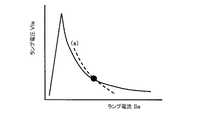
図17は従来例1で用いた蛍光ランプLAのV−I特性図(電圧−電流特性図)である。図中、最大の負抵抗の点Aは、ランプが最も不安定でありかつアーク電流及び光出力に変動を呈する可能性が非常に高い動作点である。バラストの出力インピーダンスは、ランプの最大の負抵抗の点で測定され、特に調光40%以下でバラストの出力インピーダンスは5kΩ以上とすることが好ましいと教示されている。 FIG. 17 is a VI characteristic diagram (voltage-current characteristic diagram) of the fluorescent lamp LA used in the first conventional example. In the figure, the maximum negative resistance point A is the operating point at which the lamp is most unstable and very likely to exhibit variations in arc current and light output. It is taught that the output impedance of the ballast is measured in terms of the maximum negative resistance of the lamp, and that the output impedance of the ballast is preferably 5 kΩ or more, especially at dimming of 40% or less.
図18は従来例1におけるランプのV−I特性(実線)とバラストのV−I特性(点線、一点鎖線)を示したものであり、ランプ特性とバラスト特性の交点がランプ点灯時の動作点を示している。従来例1のバラスト特性は高インピーダンス(例えば、5kΩ)時は(a)の点線で表され、ランプ電流が完全に一定となる理想的な場合には(b)の一点鎖線で表される。 FIG. 18 shows the VI characteristic (solid line) of the lamp and the ballast VI characteristic (dotted line, alternate long and short dash line) in Conventional Example 1, and the intersection of the lamp characteristic and the ballast characteristic is the operating point when the lamp is lit. Is shown. The ballast characteristic of Conventional Example 1 is represented by a dotted line (a) when the impedance is high (for example, 5 kΩ), and is represented by an alternate long and short dash line in the ideal case where the lamp current is completely constant.
(従来例2)
図19は特許文献2(特開2005−339972号公報)に開示された従来例2の回路図である。この回路では、交流電源Vsを低域通過フィルタ回路1を介して整流回路2に入力して整流し、さらにチョッパ回路3と平滑用キャパシタC0で所定の電圧の直流を得て、この平滑用キャパシタC0の両端電圧を直流電源としてハーフブリッジ形インバータ回路4に供給するようになっている。平滑用キャパシタC0の両端にはFETからなるスイッチング素子Q1,Q2と抵抗Rsとの直列回路を接続し、ローサイド側のスイッチング素子Q2と抵抗Rsの直列回路には共振用インダクタL1と共振用キャパシタC1と共振用キャパシタC1に並列接続した放電灯LAとからなる共振回路を接続し、共振用キャパシタC1の両端電圧を放電灯LAに印加するようになっている。そして、放電灯LAの出力電力を抵抗Rsの両端電圧で検出し、この両端電圧と調光レベルを決める可変の基準電圧Vrefとをフィードバック手段5の比較器を構成する誤差増幅器EAで比較してその差分に基づいた電圧信号をフィードバック信号として出力させる。そのフィードバック信号とパルス信号発生器7からの電圧信号からなる制御信号とを加算器6で加算した電圧信号に基づいて発振器8aからのパルス信号の周波数を変調するようになっている。(Conventional example 2)
FIG. 19 is a circuit diagram of Conventional Example 2 disclosed in Patent Document 2 (Japanese Patent Laid-Open No. 2005-339972). In this circuit, the AC power source Vs is input to the
ドライバ回路8bは発振器8aの発振信号に基づいてスイッチング素子Q1,Q2を交互にオン・オフ駆動するゲート信号を生成するようになっている。また、チョッパ制御回路3aはチョッパ回路3を、その出力電圧を所定電圧となるように制御するものである。なお、キャパシタCfbと抵抗Rfiは誤差増幅器EAの遅延素子を構成する。 The
図20は従来例2におけるランプのV−I特性(実線)とバラストのV−I特性(点線)を示したものであり、ランプ特性とバラスト特性の交点がランプ点灯時の動作点を示している。従来例2で示すバラストのV−I特性(点線)は、ランプ電力Wlaが一定となる制御である。このため、ランプ電力Wlaとランプ電圧Vla、ランプ電流Ilaの間には、ランプ力率を1と仮定すれば、Wla=Vla・Ila(=一定)の関係があり、VlaはIlaの逆数(1/Ila)に比例することになる。 FIG. 20 shows the VI characteristic (solid line) and the ballast VI characteristic (dotted line) of the lamp in Conventional Example 2, and the intersection of the lamp characteristic and the ballast characteristic indicates the operating point when the lamp is lit. Yes. The ballast VI characteristic (dotted line) shown in Conventional Example 2 is a control that makes the lamp power Wla constant. Therefore, if the lamp power factor is assumed to be 1 between the lamp power Wla, the lamp voltage Vla, and the lamp current Ila, there is a relationship of Wla = Vla · Ila (= constant), and Vla is the reciprocal of Ila (1 / Ila).
(従来例3)
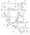
図21は特許文献3(特開2005−339976号公報)に開示された従来例3の回路図である。この放電灯点灯装置は、直流電源Eの両極間に直列接続された2つのスイッチング素子(電界効果トランジスタ)Q1,Q2からなるインバータ回路4aと、ハイサイドのスイッチング素子Q1の両端(ドレイン−ソース)間に直流カット用のコンデンサC2を介して直列接続されたインダクタL1及びコンデンサC1からなる共振回路4bと、共振用のコンデンサC1にフィラメント(図示せず)の一端が接続された放電灯(蛍光ランプ)LAの各フィラメントを予熱する予熱回路4cとを備えている。(Conventional example 3)
FIG. 21 is a circuit diagram of Conventional Example 3 disclosed in Patent Document 3 (Japanese Patent Laid-Open No. 2005-339976). This discharge lamp lighting device includes an
予熱回路4cは、共振用のインダクタL1に設けられて放電灯3のフィラメントの両端間に直列接続された二次巻線L2,L3と、各二次巻線L2,L3とフィラメントの非電源側の一端との間に挿入された直流カット用のコンデンサCf1,Cf2とで構成される。また、2つのフィラメントの非電源側の一端同士が抵抗Rdc1を介して接続され、これら2つのフィラメントの電源側には分圧抵抗Rdc2,Rdc3の直列回路及び分圧抵抗Rdc3に並列接続された平滑コンデンサCdcからなる出力検出部16が設けられ、この出力検出部16とフィラメント間に挿入された抵抗Rdc1とを介して直流電源Eから放電灯LAに直流電圧が印加されている。 The preheating
インバータ回路4aは、駆動回路8から出力する駆動信号がゲート抵抗Rg1,Rg2を介してゲートに与えられることによりスイッチング素子Q1,Q2が高周波で交互にオン・オフ(スイッチング)され、直流電源Eから供給する直流電圧を高周波電圧に変換する、所謂ハーフブリッジ形のものである。駆動回路8は例えば汎用のタイマICからなり、外付けのコンデンサCx及び3つの抵抗Rx1,Rx2,Rx3からなる周波数設定回路15により設定される周波数で発振するものであって、その発振周波数がインバータ回路4aの駆動周波数、すなわち、スイッチング素子Q1,Q2のスイッチング周波数に一致する。 In the
周波数設定回路15のコンデンサCxと抵抗Rx1〜Rx3に流れる電流の合成電流値が増加するにつれて駆動回路8の発振周波数が高くなり、駆動回路8の発振周波数、つまりインバータ回路4aの駆動周波数が高くなるにつれて共振回路4bの共振電圧が低下して放電灯LAへ供給される高周波電力も減少する。また、周波数設定回路15には図示しない調光器から抵抗Rx2を介して調光信号Vrefが入力されている。この調光信号Vrefは調光比(定格点灯時の照度を100%としたときの照度比)に比例した直流電圧からなり、調光比の低下に合わせて直流電圧レベルが小さくなるにつれて抵抗Rx2に流れる電流値が増加するため、周波数設定回路5の合成電流値が増加してインバータ回路4aの駆動周波数が高くなって放電灯LAが調光されるのである。 As the combined current value of the current flowing through the capacitor Cx and the resistors Rx1 to Rx3 of the
出力検出部16は、放電灯LAに印加される直流電圧を分圧抵抗Rdc3の電圧降下として等価的に検出するものであって、分圧抵抗Rdc3に並列接続された平滑コンデンサCdcにより検出信号を平滑化するとともに高周波ノイズを除去している。そして、この出力検出部16の検出信号が調光信号Vrefとともにフィードバック手段5に入力されている。 The
フィードバック手段5は、検出信号が入力抵抗Rinを介して反転入力端に入力されるとともに調光信号Vrefが非反転入力端に入力されるオペアンプOP1と、オペアンプOP1の出力端と反転入力端の間に並列に接続された帰還抵抗Rfb1及びコンデンサCfbで構成されており、検出信号と調光信号Vrefの電圧レベルが常に等しくなるように周波数設定回路15の電流値を増減して駆動回路8の発振周波数を調整する制御(フィードバック制御)を行うものである。 The feedback means 5 includes an operational amplifier OP1 in which the detection signal is input to the inverting input terminal via the input resistor Rin and the dimming signal Vref is input to the non-inverting input terminal, and between the output terminal and the inverting input terminal of the operational amplifier OP1. The feedback circuit Rfb1 and the capacitor Cfb are connected in parallel to each other, and the current value of the
さらに、周波数設定回路15の抵抗Rx3に対して、パルス電圧重畳回路18から周期的なパルス状の電圧を印加することでインバータ回路4aの駆動周波数を周期的に変動させ、これにより放電灯LAに印加される高周波電圧(ランプ電圧)にパルス状の高電圧(パルス電圧)を重畳させている。 Further, by periodically applying a pulsed voltage from the pulse voltage
パルス電圧重畳回路18は、オペアンプからなるバッファB1〜B3と、直流電圧信号Vdcと三角波のパルス信号Vplのうち高い方の電圧を選択するダイオードD1,D2からなり、これら2種類の信号を合成した信号であるパルス電圧指令信号Vpcが周波数設定回路15の抵抗Rx3に与えられる。パルス電圧重畳回路18から出力するパルス電圧指令信号Vpcは直流電圧信号Vdcの直流電圧レベルが大きいほど振幅が小さくなる三角波のパルス信号となる。 The pulse voltage
周波数設定回路15はフィードバック手段5の出力電圧レベルにより調光信号Vrefの調光比に応じた値に駆動回路8の発振周波数を設定するとともに、パルス電圧重畳回路18のパルス電圧指令信号Vpcのパルス振幅に応じた周波数分だけ発振周波数を周期的に低い値に変化させる。その結果、発振周波数が周期的に小さい値に変化したときにインバータ回路4aから共振回路4bを介して放電灯LAに印加されるランプ電圧Vlaにパルス電圧が重畳されることになる。 The
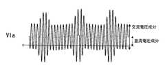
放電灯LAのランプ電圧Vlaは図22に示すような波形となる。放電が不安定になりやすい調光比ではパルス電圧のピーク値を増加させ、放電が最も不安定になりやすい調光比においても放電灯LAの点灯維持に必要十分なパルス電圧を印加することにより放電灯LAを安定点灯することができる。 The lamp voltage Vla of the discharge lamp LA has a waveform as shown in FIG. By adjusting the pulse voltage at the dimming ratio at which the discharge tends to become unstable, and by applying a pulse voltage sufficient to maintain the lighting of the discharge lamp LA even at the dimming ratio at which the discharge is most unstable. The discharge lamp LA can be stably lit.
従来例1や従来例2では、各々ランプ電流Ilaをフィードバックして一定化したり、ランプ電力Wlaをフィードバックして一定化しているため、調光レベルの低い点でも比較的安定に点灯できる。しかし、それらの下限より更に低光束まで調光を深くしようとすると、やはりランプのV−I特性とバラストのV−I特性が乖離を起こし、結果的にランプの立ち消えやちらつき、動作点のジャンプといった望ましくない現象が発生してしまう。 In the conventional example 1 and the conventional example 2, the lamp current Ila is fed back and fixed, or the lamp power Wla is fed back and fixed, so that the lamp can be lit relatively stably even at a low dimming level. However, if the dimming is further increased to a lower luminous flux than the lower limit, the VI characteristic of the lamp and the VI characteristic of the ballast will be different from each other. Such an undesirable phenomenon occurs.
また、従来例3の場合、直流電圧成分の重畳やパルス状電圧の印加によって、低光束まで安定に点灯できるものの、制御回路が複雑化する。また、直流電圧成分の重畳によりランプのカタホレシス現象が発生しやすくなる、などの欠点が生じる。 Further, in the case of the conventional example 3, although it is possible to stably light up to a low luminous flux by superimposing a DC voltage component or applying a pulse voltage, the control circuit is complicated. In addition, there is a disadvantage that the cataphoresis phenomenon of the lamp is likely to occur due to the superposition of the DC voltage component.
本発明はこのような点に鑑みてなされたものであり、直流電圧やパルス電圧を重畳させなくても、従来のランプ電流またはランプ電力を一定化する制御に比べて、さらに低光束まで安定して調光点灯させることが可能な低圧放電灯点灯装置を提供することを課題とする。 The present invention has been made in view of such a point, and even without superimposing a DC voltage or a pulse voltage, the present invention is more stable to a lower luminous flux than the conventional control that makes the lamp current or lamp power constant. It is an object of the present invention to provide a low pressure discharge lamp lighting device capable of dimming lighting.
請求項1の発明は、上記の課題を解決するために、図1に示すように、直流電圧源Vdcから出力される直流電圧をスイッチングする1つ以上のスイッチング素子Q1,Q2と、前記スイッチング素子Q1,Q2を高周波でオン・オフする駆動回路8と、前記スイッチング素子Q1,Q2によりスイッチングされた電圧を印加されて放電灯LAに共振電圧を供給する共振回路(インダクタL1、コンデンサC1)とで構成されるインバータ回路4を備える放電灯点灯装置において、放電灯LAの電圧−電流特性との交点における前記インバータ回路4の電圧−電流特性の傾きが略一定の正の値となるように、前記直流電圧源Vdcから出力される直流電圧または前記スイッチング素子Q1,Q2のオン・オフを調整するフィードバック手段5を設けたことを特徴とするものである。 In order to solve the above-described problem, the invention of
請求項2の発明は、請求項1の発明において、前記放電灯LAの電圧−電流特性との交点における前記インバータ回路4の電圧−電流特性を1次関数式で表したとき、その切片を調光器9で実質的に可変とすることを特徴とする。 According to a second aspect of the invention, in the first aspect of the invention, when the voltage-current characteristic of the
請求項3の発明は、請求項2の発明において、前記調光器9によって調整される1次関数式の切片は、連続的に可変とするか、または、調光時の設定値が定格点灯時の設定値の整数分の1になっていることを特徴とする。 According to a third aspect of the present invention, in the second aspect of the invention, the intercept of the linear function equation adjusted by the dimmer 9 is continuously variable, or the set value during dimming is rated lighting It is characterized by being 1 / integer of the set value of the hour.
請求項4の発明は、請求項1〜3の発明において、図6〜図8に示すように、前記フィードバック手段5のゲインを調光のレベルに応じて変化させることを特徴とする。 According to a fourth aspect of the invention, in the first to third aspects of the invention, as shown in FIGS. 6 to 8, the gain of the feedback means 5 is changed in accordance with the dimming level.
請求項5の発明は、請求項1〜4の発明において、図9、図10に示すように、前記フィードバック手段5の機能を放電灯LAの始動前はオフにし、放電灯LAの始動後にオンにすることを特徴とする。 According to a fifth aspect of the present invention, in the first to fourth aspects of the present invention, as shown in FIGS. 9 and 10, the function of the feedback means 5 is turned off before the discharge lamp LA is started and turned on after the discharge lamp LA is started. It is characterized by.
請求項6の発明は、請求項1〜5の発明において、図11、図12に示すように、前記フィードバック手段5は、放電灯LAの電圧−電流特性との交点における前記インバータ回路4の電圧−電流特性の傾きが略一定の正の値となるように、前記直流電圧源Vdcから出力される直流電圧または前記スイッチング素子Q1,Q2のオン・オフを調整する第1のフィードバック機能と、放電灯LAの電流Ilaの検出値が略一定となるように、前記直流電圧源Vdcから出力される直流電圧または前記スイッチング素子Q1,Q2のオン・オフを調整する第2のフィードバック機能を、調光レベルに応じて切り替え可能としたことを特徴とする。 According to a sixth aspect of the present invention, in the first to fifth aspects of the present invention, as shown in FIGS. 11 and 12, the feedback means 5 has a voltage of the
請求項7の発明は、請求項1〜6の発明において、図13に示すように、ランプ電圧検出手段11またはランプ電流検出手段13を備え、ランプ電圧またはランプ電流のいずれかの検出信号が所定の閾値以上になると、インバータ回路4の出力を抑制するか、又は停止させる異常検出回路51を設けたことを特徴とする。 As shown in FIG. 13, the invention of claim 7 comprises lamp voltage detection means 11 or lamp current detection means 13 as shown in FIG. 13, and a detection signal of either lamp voltage or lamp current is predetermined. An
請求項8の発明は、請求項1〜7の発明において、放電灯LAの電圧−電流特性との交点におけるインバータ回路4の電圧−電流特性の傾きを演算する手段10は、除算用アナログIC、またはマイコン、またはデジタル・シグナル・プロセッサのいずれかであることを特徴とする。 According to an eighth aspect of the present invention, in the first to seventh aspects of the present invention, the
請求項9の発明は、請求項1〜8の発明において、図14に示すように、センサ17を備え、センサ17の出力に応じて調光レベルを変化させることを特徴とする。 The invention of claim 9 is characterized in that, in the inventions of
請求項10の発明は、請求項1〜9のいずれかに記載の低圧放電灯点灯装置が組み込まれた照明器具である(図15)。 The invention of
請求項1の発明によれば、放電灯の電圧−電流特性との交点におけるインバータ回路の電圧−電流特性の傾きが略一定の正の値となるように、直流電圧源から出力される直流電圧またはインバータ回路のスイッチング素子のオン・オフを調整するフィードバック手段を設けたから、従来のランプ電流フィードバックやランプ電力フィードバックといった制御に比べ、放電灯の電圧−電流特性とインバータ回路の電圧−電流特性の交点がより安定的に形成され、より低光束までの調光が可能となる。 According to the first aspect of the present invention, the DC voltage output from the DC voltage source is such that the slope of the voltage-current characteristic of the inverter circuit at the intersection with the voltage-current characteristic of the discharge lamp becomes a substantially constant positive value. Or, since a feedback means for adjusting on / off of the switching element of the inverter circuit is provided, the intersection of the voltage-current characteristic of the discharge lamp and the voltage-current characteristic of the inverter circuit compared to the conventional control such as lamp current feedback and lamp power feedback. Can be more stably formed, and light control up to a lower luminous flux becomes possible.
請求項2または3の発明によれば、調光下限の光出力の調整が細かく行える。
請求項4の発明によれば、定格付近で無理にゲインを上げる必要がないので、フィードバック手段での発散が起こりにくい。また、調光が深いほどゲインを高くすることで、より立消えに強くなる。
請求項5の発明によれば、ランプが確実に始動してから、調光時に立消えしにくい本発明の制御を開始できる。According to the invention of
According to the invention of
According to the invention of
請求項6の発明によれば、定格電流が同じで定格電力が異なるランプを同一のインバータ回路で点灯することができ、かつ調光時に立消えしにくい利点がある。
請求項7の発明によれば、無負荷時やフィードバック手段での発散による異常時などに安全に回路の発振を弱めたり、停止したりできる。また、ランプ電圧検出手段またはランプ電流検出手段を異常検出回路と兼用することで、回路の簡易化が図れる。
請求項9の発明によれば、センサによる補正により照度を一定化したまま、低光束調光が可能である。According to the invention of claim 6, lamps having the same rated current and different rated power can be lit with the same inverter circuit, and there is an advantage that the lamps are not easily extinguished during dimming.
According to the invention of claim 7, the oscillation of the circuit can be weakened or stopped safely when there is no load or when there is an abnormality due to divergence by the feedback means. Further, the circuit can be simplified by using the lamp voltage detecting means or the lamp current detecting means also as the abnormality detecting circuit.
According to the ninth aspect of the present invention, low beam dimming can be performed while the illuminance is kept constant by correction by the sensor.
(実施形態1)
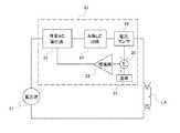
図1は本発明の実施形態1の基本構成を示す回路図である。直流電圧源Vdcには、スイッチング素子Q1、Q2の直列回路が接続されている。スイッチング素子Q1、Q2は駆動回路8により高周波でオン・オフされる。スイッチング素子Q1、Q2の接続点と直流電圧源Vdcの一端(ここでは負極)の間にはインダクタL1とコンデンサC1の直列共振回路が接続されている。コンデンサC1の一端にコンデンサC2の一端が接続されている。以上の回路により電子安定器(バラスト)としてのインバータ回路4を構成している。(Embodiment 1)
FIG. 1 is a circuit diagram showing a basic configuration of
また、コンデンサC2の他端とスイッチング素子Q2のソース側端子間に蛍光ランプLAが接続されている。蛍光ランプLAには、ランプ電圧Vlaを検出するVla検出回路11が接続されている。Vla検出回路11の出力には、ランプ電圧Vlaの変化量を検出するΔVla検出回路12が接続されている。蛍光ランプLAのランプ電流経路には、ランプ電流Ilaを検出するIla検出回路13が接続されている。Ila検出回路13の出力には、ランプ電流Ilaの変化量を検出するΔIla検出回路14が接続されている。ΔVla検出回路12の出力と、ΔIla検出回路14の出力は演算手段10に入力されている。演算手段10はΔVlaの値をΔIlaの値で除算する演算手段である。 A fluorescent lamp LA is connected between the other end of the capacitor C2 and the source side terminal of the switching element Q2. A
上記演算手段10の出力信号はフィードバック手段5に入力されて、抵抗Rを介してオペアンプOPのマイナス側入力端子に印加されている。オペアンプOPのプラス側入力端子には調整可能な直流電圧αが基準電圧として印加されている。オペアンプOPのマイナス側入力端子と出力端子間にはコンデンサC3が接続され、いわゆる積分回路を構成している。また、オペアンプOPの出力はインバータ回路4の駆動回路8に入力され、ΔVla/ΔIlaが直流電圧αに応じた目標値に一致するようにフィードバック系が構成されている。ΔVla/ΔIlaはバラスト特性の傾きを示すものであり、これを基準値と等しくなるようにオペアンプOPによりフィードバック制御する。ここでは駆動回路8によりインバータ回路4のスイッチング周波数を制御しているが、スイッチング素子Q1,Q2のオン時間幅(デューティ)を制御しても良いし、直流電圧源Vdcの電圧を制御するように構成しても良い。 The output signal of the
また、ランプ電流Ilaを調整するために、Ila検出回路13の出力がフィードバック手段5に入力されて、抵抗R2を介してオペアンプOP2のマイナス側入力端子に印加されている。オペアンプOP2のプラス側入力端子には調光器9によって調整可能な直流電圧Vdimが基準電圧として印加されている。オペアンプOP2のマイナス側入力端子と出力端子間にはコンデンサC4が接続され、いわゆる積分回路を構成している。オペアンプOP2の出力はインバータ回路4の直流電圧源Vdcに帰還入力され、ランプ電流Ilaが直流電圧Vdimに応じた目標値に一致するようにフィードバック系が構成されている。 In order to adjust the lamp current Ila, the output of the
直流電圧源Vdcは、例えば商用電源から昇圧チョッパ回路等のPFC回路(力率改善制御回路)を介して得ることができ、その電圧を調整するには、PFC回路のスイッチング要素の周波数やデューティを変化させるなどすれば良い。調光の目標値となる直流電圧Vdimは、インバータ回路4の外部に設置された調光器9によって、その値を可変できるようになっている。 The DC voltage source Vdc can be obtained, for example, from a commercial power supply through a PFC circuit (power factor correction control circuit) such as a boost chopper circuit. To adjust the voltage, the frequency and duty of the switching element of the PFC circuit are adjusted. Change it. The DC voltage Vdim, which is a target value for dimming, can be varied by a dimmer 9 installed outside the
以下、本実施形態の動作について説明する。蛍光ランプLAの点灯時に、Vla検出回路11でランプ電圧Vlaの実効値に相当する電圧を検出し、Ila検出回路13でランプ電流Ilaの実効値に相当する電圧を検出する。更に、ΔVla検出回路12でランプ電圧Vlaの変化量ΔVlaを、ΔIla検出回路14でランプ電流Ilaの変化量ΔIlaを検出する。変化量ΔVla、ΔIlaは単位時間当たりの変化量を求めれば良い。そして、演算手段10により、ΔVla/ΔIlaを演算する。なお、特殊な場合としてΔIla=0の場合には、ランプの状態が安定していると言えるので、フィードバック制御は収束したものとみなして、演算手段10は目標値αを出力するように構成すれば良い。本発明は低光束時にはランプ電流Ilaが不安定となることを前提としているので、通常はΔIla≠0であり、ΔVla/ΔIlaの演算は可能である。 Hereinafter, the operation of this embodiment will be described. When the fluorescent lamp LA is turned on, the
上記オペアンプOPと抵抗R、コンデンサC3で構成される積分回路の動作により、演算手段10の出力ΔVla/ΔIlaは直流電圧αに略等しくなるようにフィードバック制御される。また、同時にオペアンプOP2でIla検出回路13からの検出信号をフィードバックして、ランプ電流Ilaの調整を行う。 By the operation of the integrating circuit composed of the operational amplifier OP, the resistor R, and the capacitor C3, feedback control is performed so that the output ΔVla / ΔIla of the computing means 10 becomes substantially equal to the DC voltage α. At the same time, the operational amplifier OP2 feeds back the detection signal from the
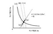
以上の動作を、図2を用いて具体的に説明する。図2は、横軸をランプ電流Ila、縦軸をランプ電圧VlaとしたときのV−I特性を示すもので、図中の(a)、(b)はバラストのV−I特性、図中の(c)はランプのV−I特性である。また、図中の一点鎖線は、フィードバック手段5の働いていない、所謂オープン状態におけるバラストのV−I特性(スイッチング周波数が一定の条件)を示している。 The above operation will be specifically described with reference to FIG. FIG. 2 shows the VI characteristics when the horizontal axis is the lamp current Ila and the vertical axis is the lamp voltage Vla, where (a) and (b) are the ballast VI characteristics, (C) is the VI characteristic of the lamp. Also, the alternate long and short dash line in the figure indicates the ballast VI characteristics (conditions where the switching frequency is constant) in a so-called open state where the feedback means 5 is not working.
先述した演算手段10のΔVla/ΔIlaというのは、バラストのV−I特性の傾きを演算していることに他ならない。したがって、このΔVla/ΔIlaが一定に制御される場合、バラストのV−I特性は図2の(a)や(b)で示すような傾きが一定の直線になる。ランプ点灯時の動作点は、ランプのV−I特性とバラストのV−I特性の交点であるので、図中の(a)と(c)の交点や(b)と(c)の交点が点灯時の動作点となる。 The aforementioned ΔVla / ΔIla of the computing means 10 is nothing but computing the slope of the ballast VI characteristic. Therefore, when this ΔVla / ΔIla is controlled to be constant, the V-I characteristic of the ballast is a straight line having a constant slope as shown in (a) and (b) of FIG. Since the operating point when the lamp is lit is the intersection of the VI characteristic of the lamp and the VI characteristic of the ballast, the intersection of (a) and (c) or the intersection of (b) and (c) in the figure is This is the operating point when lit.
調光器9により直流電圧Vdimを変化させることにより、バラストのV−I特性は図2の(a)や(b)で示すように傾きが一定で、切片が増減する1次関数となり、任意に調光が可能である。調光器9の出力信号は、直流電圧やPWM信号、あるいはバイナリーコードなどのデジタル信号であっても良い。 By changing the DC voltage Vdim by the dimmer 9, the V-I characteristic of the ballast becomes a linear function with a constant slope and an increasing / decreasing intercept as shown in FIGS. 2 (a) and (b). Dimming is possible. The output signal of the dimmer 9 may be a DC signal, a PWM signal, or a digital signal such as a binary code.
図3は、図2の交点付近を拡大表示した図である。図中の実線はランプのV−I特性、点線はバラストのV−I特性、一点鎖線は周波数一定条件下でのオープン状態でのバラストのV−I特性である。動作点である一点鎖線(ロ)とランプのV−I特性の交点付近において、バラストのV−I特性(点線)上の(a)、(b)間の往復を繰返し、最終的には(ロ)点に収束する。フィードバック系のゲインが大きいほど、この(a)⇔(b)間の往復幅は小さくなり、素早く収束することになる。ただし、ゲインを大きくし過ぎると、系が発散して交点から外れやすくなる。 FIG. 3 is an enlarged view of the vicinity of the intersection in FIG. In the figure, the solid line represents the V-I characteristic of the lamp, the dotted line represents the V-I characteristic of the ballast, and the alternate long and short dash line represents the V-I characteristic of the ballast in the open state under a constant frequency condition. The round trip between (a) and (b) on the VI characteristic (dotted line) of the ballast is repeated in the vicinity of the intersection of the dot-and-dash line (B) as the operating point and the VI characteristic of the lamp. B) It converges to a point. As the gain of the feedback system is larger, the reciprocal width between (a) and (b) is smaller and converges quickly. However, if the gain is increased too much, the system diverges and tends to deviate from the intersection.
ちなみに、交点を外れた場合には、バラストのV−I特性の点線上を無限に大きくなる方向へ進むわけではなく、外れた時点でのオープン状態での共振系(図中の一点鎖線)上の軌跡を推移することになる。例えば、(b)点で外れた場合には(ハ)上を上方向へ推移する。これは、フィードバック系を用いない場合の無負荷状態と同じであり、ランプ電圧を検出して発振を停止させるなどの従来からの無負荷検出回路で対応することができる。 By the way, when the point of intersection is deviated, it does not travel in the direction of increasing infinitely on the dotted line of the ballast VI characteristic, but on the resonance system (one-dot chain line in the figure) in the open state at the point of deviating. The trajectory will be changed. For example, when the point is deviated at point (b), (c) moves upward. This is the same as the no-load state when the feedback system is not used, and can be dealt with by a conventional no-load detection circuit that stops the oscillation by detecting the lamp voltage.
これまでの説明により、特に調光下限付近において、ランプ電流を一定化する制御(従来例1)やランプ電力を一定化する制御(従来例2)に比べて、ランプのV−I特性とバラストのV−I特性がさらにより垂直的に交わるため、動作点が安定的に形成され、調光下限をより深くすることができる。 According to the above description, especially in the vicinity of the dimming lower limit, the V-I characteristic and ballast of the lamp are compared with the control for making the lamp current constant (conventional example 1) and the control for making the lamp power constant (conventional example 2). Therefore, the operating point is stably formed, and the lower limit of dimming can be made deeper.
演算手段10にはアナログの除算器を用いても良く、あるいは、デジタルの除算器としてマイコンやDSP(デジタル・シグナル・プロセッサ)などを用いても良い。ΔVla/ΔIla一定化手段としてのフィードバック手段5もデジタル的に処理することが可能なため、調光器9からの入力もすべてデジタル信号に統一すれば、フィードバック回路全体がデジタル処理できることになり、全てをマイコン内で処理することができ、回路が簡易になり、小型化が実現可能である。 An analog divider may be used for the
なお、検出回路11,13の出力は、例えば実効値に相当するような直流値とすることが望ましい。なぜなら、瞬時値で演算することも可能であり、その方が収束性は早まるが、瞬時値の場合は交流の正負が反転する際にランプ電流=0となる点があるため除算時の出力が発散しやすくなり、それを補正する回路が別途必要になるためである。 Note that the outputs of the
負荷LAが熱陰極型の蛍光ランプである場合、一般的に用いられているような調光に応じて予熱電流を増加させるような制御を組み合わせることで、更に低光束時の点灯安定性が高まる。 When the load LA is a hot cathode fluorescent lamp, the lighting stability at the time of a low luminous flux is further improved by combining the control for increasing the preheating current in accordance with dimming as generally used. .
図4は、調光器9を用いた調光方法に関する説明図である。これまでに述べた制御に従い、図1における直流電圧Vdimを調光器9で連続的に変化させることで、バラスト特性の切片が実質上連続的に変化し、その結果、調光動作も連続的に行われることになる。これは、特にアナログ的に調光レベルを変化させる場合に適している。ところが、例えば、段調光であったり、マイコンなどを用いてデジタル的に制御する場合などでは、調光レベルの指令値は離散的になる。 FIG. 4 is an explanatory diagram relating to a dimming method using the dimmer 9. In accordance with the control described so far, the DC voltage Vdim in FIG. 1 is continuously changed by the dimmer 9, so that the intercept of the ballast characteristic is substantially continuously changed. As a result, the dimming operation is also continuously performed. Will be done. This is particularly suitable when the dimming level is changed in an analog manner. However, for example, in case of step dimming or digital control using a microcomputer or the like, the dimming level command value is discrete.
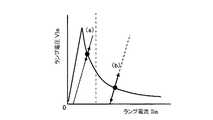
図4において、定格点灯時の動作点を(a)とし、このときの基準電圧がN(V)であったとする。この点から調光する際、指令値をN/2、N/3、N/4、…と一定間隔で変化させたのが図4であり、定格点灯時の動作点(a)から始まって、(b)、(c)、(d)、(e)、…となるにつれ、調光が深くなっていく。各バラスト特性の切片は1/2倍、1/3倍、…と減少する一方で、ランプのV−I特性は図4に示すように下に凸の単調減少の曲線で表されるため、定格付近での変化幅に比べ、調光下限付近の調光幅の方が細かくなる。このため、調光下限付近における調光が自動的に狭い間隔で調整可能となり、動作ポイントの急変による立消えやジャンプが起こりにくくなる。 In FIG. 4, it is assumed that the operating point at rated lighting is (a) and the reference voltage at this time is N (V). When dimming from this point, the command value is changed at regular intervals of N / 2, N / 3, N / 4,..., Starting from the operating point (a) at rated lighting. , (B), (c), (d), (e),..., The light control becomes deeper. While the intercept of each ballast characteristic decreases to 1/2 times, 1/3 times,..., The V-I characteristic of the lamp is represented by a monotonously decreasing curve convex downward as shown in FIG. The dimming width near the lower limit of dimming is smaller than the change width near the rating. For this reason, the dimming in the vicinity of the dimming lower limit can be automatically adjusted at a narrow interval, and the disappearance or jump due to the sudden change of the operating point is less likely to occur.
以上のように、本実施形態によれば、ランプのV−I特性とバラストのV−I特性の交点が垂直的に近づくため低光束まで調光可能である。特に低光束領域で、オープン制御とした場合のようにランプのV−I特性とバラストのV−I特性の交点を2つ持つことがないため、動作点がジャンプしにくい。また、無負荷などでフィードバック制御が外れた(閉ループが発散した)場合、動作点はLC共振系上を推移するため、従来と同じ無負荷検出回路(例えばVla検知)で停止させることにより安全性が確保される。 As described above, according to the present embodiment, since the intersection point of the VI characteristic of the lamp and the VI characteristic of the ballast approaches vertically, the light can be adjusted to a low luminous flux. In particular, in the low light flux region, there is no two intersections between the lamp VI characteristic and the ballast VI characteristic unlike in the case of open control, so that the operating point is difficult to jump. Also, when feedback control is lost due to no load (closed loop diverges), the operating point shifts on the LC resonance system, so it is safer to stop by the same no-load detection circuit (for example, Vla detection) as before. Is secured.
以上の動作は簡易なフィードバック回路で実現可能であり、除算機能はマイコンなどで安価に実現できるから、コストダウンが可能となる。さらに、負荷が熱陰極型の蛍光ランプである場合には、調光下限付近ほど予熱電流を増加させるなどの予熱電流制御との組合せにより、更に低光束時の点灯安定性が高まる。 The above operation can be realized by a simple feedback circuit, and the division function can be realized at low cost by a microcomputer or the like, so that the cost can be reduced. Further, when the load is a hot cathode fluorescent lamp, the lighting stability at the time of low luminous flux is further enhanced by the combination with the preheating current control such as increasing the preheating current near the dimming lower limit.
(実施形態1’)
図5は実施形態1の一変形例の回路図である。図1の基本回路構成では、バラストのV−I特性の傾きを一定化するフィードバック・ループと、ランプ電流Ilaを調整するフィードバック・ループが別々に設けられているが、図5の回路では、図1におけるオペアンプOP、オペアンプOP2を用いた2つのフィードバック・ループを一つにまとめた例である。(Embodiment 1 ')
FIG. 5 is a circuit diagram of a modification of the first embodiment. In the basic circuit configuration of FIG. 1, a feedback loop that stabilizes the slope of the ballast VI characteristic and a feedback loop that adjusts the lamp current Ila are provided separately. In the circuit of FIG. 2 is an example in which two feedback loops using the operational amplifier OP and the operational amplifier OP2 are combined into one.
演算手段10の出力はフィードバック手段5の加算器5aに入力されている。更に、ランプ電流Ilaを調整するために、Ila検出回路13の出力が加算器5aに入力されて、演算手段10の出力に加算されている。加算器5aの出力信号は、入力抵抗Rを介してオペアンプOPのマイナス側入力端子に印加されている。オペアンプOPのプラス側入力端子には調光器9によって調整可能な基準電圧となる直流電圧αが印加されている。オペアンプOPのマイナス側入力端子と出力端子間にはコンデンサC3が接続され、いわゆる積分回路を構成している。また、オペアンプOPの出力がインバータ回路4の駆動回路8に入力され、ΔVla/ΔIlaが直流電圧αに応じた目標値に一致するようにフィードバック系が構成されている。直流電圧αはインバータ回路4の外部に設置された調光器9によって、その値を可変できるようになっている。 The output of the
図5の例では、傾きを一定化するフィードバック・ループとランプ電流Ilaを調整するフィードバック・ループを1つのオペアンプOPにより兼用したため、調光に伴ってバラストのV−I特性の傾きも若干変化するが、図1に示した基本回路構成であれば、調光全区間で傾きを一定にできる。 In the example of FIG. 5, the feedback loop that stabilizes the slope and the feedback loop that adjusts the lamp current Ila are shared by one operational amplifier OP, so that the slope of the ballast VI characteristic slightly changes with dimming. However, with the basic circuit configuration shown in FIG. 1, the inclination can be made constant in the entire dimming section.
以下に述べる実施形態では、バラストのV−I特性の傾きを一定化するフィードバック・ループと、ランプ電流Ilaを調整するフィードバック・ループを兼用した図5の構成について、種々の変形例を説明するが、2つのフィードバック・ループを別々に設けても良いことは言うまでも無い。 In the embodiment described below, various modifications will be described with respect to the configuration of FIG. 5 that also serves as a feedback loop that stabilizes the slope of the ballast VI characteristic and a feedback loop that adjusts the lamp current Ila. Needless to say, the two feedback loops may be provided separately.
(実施形態2)
図6は本発明の実施形態2の回路図である。図5に示した構成と異なる点は、抵抗Rと直列に抵抗R’が接続されており、抵抗R’と並列にスイッチSW1が接続されている点である。スイッチSW1は調光器9の信号に応じて、オン・オフを切り替えられる。他の構成は図5と同じであるため、重複する説明を省略する。(Embodiment 2)
FIG. 6 is a circuit diagram of
本実施形態は、調光動作の途中でフィードバックのゲインを変化させる例である。スイッチSW1がオンのときは、抵抗R’が短絡されているため、回路動作としては図5と同様となる。このとき、フィードバック手段5の積分ゲインG1は、G1=1/(2πf・C3・R)となる。ここで、fは周波数である。 The present embodiment is an example in which the gain of feedback is changed during the dimming operation. When the switch SW1 is on, the resistor R 'is short-circuited, so that the circuit operation is the same as in FIG. At this time, the integral gain G1 of the feedback means 5 is G1 = 1 / (2πf · C3 · R). Here, f is a frequency.
スイッチSW1がオフのときは、抵抗R’が開放のため、フィードバック手段5の積分ゲインG2は、G2=1/(2πf・C3・(R+R’))となる。したがって、スイッチSW1をオフしたときの方が、積分ゲインが小さくなる。 When the switch SW1 is off, the resistor R 'is open, and the integral gain G2 of the feedback means 5 is G2 = 1 / (2πf · C3 · (R + R ′)). Therefore, the integral gain is smaller when the switch SW1 is turned off.
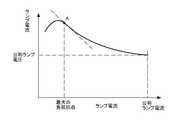
図7を用いて具体的な回路動作を説明する。調光レベルに応じてスイッチSW1のオン、オフが切替わるように設定する。一点鎖線より左側ではスイッチSW1はオン、一点鎖線より右側ではスイッチSW1はオフとなるように制御する。このように制御することにより、定格点灯付近では比較的緩いフィードバック・ゲインで制御され、調光が深い領域では、比較的強いフィードバック・ゲインで制御される。上記フィードバック・ゲインの大小を図7では概念的に矢印の長さで示している。矢印が長い程、収束するまでに時間が掛かることを示している。 A specific circuit operation will be described with reference to FIG. It is set so that the switch SW1 is switched on and off according to the dimming level. Control is performed so that the switch SW1 is turned on on the left side of the alternate long and short dash line and the switch SW1 is turned off on the right side of the alternate long and short dash line. By controlling in this way, control is performed with a relatively loose feedback gain in the vicinity of the rated lighting, and control is performed with a relatively strong feedback gain in a region where light control is deep. The magnitude of the feedback gain is conceptually shown by the length of the arrow in FIG. The longer the arrow, the longer it takes to converge.
図8はゲインを変化させる別の例について、ランプ電流IlaとゲインGの関係だけ示している。図中(b)の一点鎖線は定格点灯時を示しており、また、(a)の一点鎖線はゲインの増減の折り返し点を示している。定格点灯での動作点から徐々に調光させていくと、バラストのV−I特性とランプのV−I特性の(接線の)交点の角度は、鈍角(鋭角)より徐々に垂直に変化し、それを過ぎると鋭角(鈍角)になっていく。このため、最も垂直になる点でのゲインは(a)点で示すようにゲインを最小値にしておき、その点より離れる度合に応じてゲインを連続的に上げる。なお、図8の動作を実現するための回路は図示していないが、先述のスイッチSW1の代わりに抵抗Rを連続的に可変制御したり、あるいはコンデンサC3の容量を連続的に可変制御するように構成すれば良い。 FIG. 8 shows only the relationship between the lamp current Ila and the gain G for another example of changing the gain. In the figure, the alternate long and short dash line in (b) indicates the rated lighting, and the alternate long and short dash line in (a) indicates the turning point of the gain increase and decrease. When dimming gradually from the operating point at the rated lighting, the angle of the intersection of the ballast VI characteristic and the lamp VI characteristic (tangent) gradually changes vertically from the obtuse angle (acute angle). After that, it becomes an acute angle (obtuse angle). For this reason, the gain at the most vertical point is set to the minimum value as shown by the point (a), and the gain is continuously increased according to the degree of separation from the point. Although a circuit for realizing the operation of FIG. 8 is not shown, the resistor R is continuously variably controlled instead of the above-described switch SW1, or the capacitance of the capacitor C3 is continuously variably controlled. What is necessary is just to comprise.
本実施形態によれば、定格付近で無理にフィードバック手段のゲインを上げる必要がないので、フィードバック手段での発散が起こりにくい。また、調光が深いほど、ゲインを高くすることで、より立消えに強くなる。さらに、ゲインの最小点をバラストのV−I特性とランプのV−I特性(の接線)が垂直に交わる点とし、そこから離れるほどゲインを高くすることで、調光の全区間に渡って、立消えしにくくなる。 According to the present embodiment, there is no need to forcibly increase the gain of the feedback means near the rating, and therefore the divergence of the feedback means is unlikely to occur. In addition, the deeper the dimming, the higher the gain, and the stronger the dimming. Furthermore, the minimum point of the gain is defined as a point where the ballast VI characteristic and the lamp VI characteristic (tangent line) intersect perpendicularly, and the gain increases with increasing distance from the point, so that the entire dimming interval is achieved. It becomes difficult to disappear.
(実施形態3)
図9は本発明の実施形態3の回路図である。図5と異なる点は、フィードバック手段5の出力と駆動回路8の入力の間にスイッチSW2を挿入し、Ila検出回路13の検出出力に応じて、スイッチSW2のオン・オフを切り替える回路を追加した点である。他の部分は図5と同じであるため、重複する説明は省略する。(Embodiment 3)
FIG. 9 is a circuit diagram of
本実施形態は、予熱、始動、点灯といったシーケンスを伴う熱陰極型の蛍光ランプの具体的な始動制御の一例である。これまで述べてきた動作は点灯中におけるものであり、ランプが始動するまでは動作しないことが望ましい。そのため、ランプLAが高電圧印加によって始動するまでは、スイッチSW2をオフして、フィードバック制御を確実に不動作にしておき、始動後、ランプ電流が流れているのを検知してからスイッチSW2をオンに切り替えることにより、これまで述べてきたフィードバック動作を開始させる。 The present embodiment is an example of specific starting control of a hot cathode fluorescent lamp with sequences such as preheating, starting, and lighting. The operation described so far is during lighting, and it is desirable that it does not operate until the lamp is started. Therefore, until the lamp LA is started by applying a high voltage, the switch SW2 is turned off and the feedback control is surely disabled. After the start, the switch SW2 is turned on after detecting that the lamp current is flowing. By switching on, the feedback operation described so far is started.
図10により本実施形態の動作を説明する。図中、(a)はスイッチSW2のオン・オフ状態であり、(b)はランプ端に印加される電圧を示している。予熱時はランプ端に電圧が印加され、ランプのフィラメントに予熱電流が流れるが、ランプ電流は流れない。始動時にランプ端に高圧の電圧が印加されて、ランプ内部で放電破壊を生じ、ランプ電流が流れ始める。このランプ電流が流れ始めたことをIla検出回路13で検知して、スイッチSW2をオンさせる。点灯後の動作はこれまで述べてきたのと同様である。 The operation of this embodiment will be described with reference to FIG. In the figure, (a) shows the on / off state of the switch SW2, and (b) shows the voltage applied to the lamp end. During preheating, a voltage is applied to the lamp end, and a preheating current flows through the filament of the lamp, but no lamp current flows. When starting, a high voltage is applied to the end of the lamp, causing a discharge breakdown inside the lamp, and a lamp current starts to flow. The
本実施形態によれば、ランプが確実に始動してから、調光時の立消えに強い本発明のフィードバック制御を開始できる。 According to this embodiment, after the lamp has been reliably started, the feedback control of the present invention that is resistant to extinction during dimming can be started.
(実施形態4)
図11は本発明の実施形態4の回路図である。図5と異なる点は、フィードバック手段5の入力として、Ila検出回路13の出力と演算手段10の出力とが選択的に切替可能なスイッチSW3を設け、調光器9の出力に応じて、スイッチSW3を切り替える回路を追加した点である。他の部分は図5と同じであるため、重複する説明は省略する。(Embodiment 4)
FIG. 11 is a circuit diagram of
本実施形態は、調光レベルに応じてフィードバック制御の対象を切り替える例である。すなわち、調光レベルに応じて、スイッチSW3を切替えることで、スイッチSW3がIla検出回路13の出力に接続されているときには、ランプ電流Ilaが一定となるように制御され、スイッチSW3が演算手段10の出力に接続されているときには、バラストのV−I特性の傾きが一定となるように制御される。 The present embodiment is an example in which the target of feedback control is switched according to the dimming level. That is, by switching the switch SW3 according to the dimming level, when the switch SW3 is connected to the output of the
図12は、本実施形態の制御を適用した場合の動作説明図である。調光レベルに応じて、一点鎖線より右側ではスイッチSW3をIla検出回路13の側に、一点鎖線より左側ではスイッチSW3を演算手段10の側に切替えることで、定格付近の(イ)点では、ランプ電流Ilaが一定となるようにフィードバック制御される。また、深い調光時の(ロ)点や(ハ)点では、バラストのV−I特性の傾きが一定となるように制御される。 FIG. 12 is an operation explanatory diagram when the control of the present embodiment is applied. By switching the switch SW3 to the
このように制御することで、例えば、定格電流が同じで定格電力が異なるランプを同一のインバータ回路で点灯させることが可能であり、かつ、調光時には、これまで述べたように立消えに強い回路を構成することができる。 By controlling in this way, for example, it is possible to turn on lamps with the same rated current but different rated power with the same inverter circuit, and at the time of dimming, a circuit that is resistant to extinction as described above Can be configured.
なお、本実施形態では、バラストのV−I特性の傾きを一定化するフィードバック制御と、ランプ電流Ilaを一定化するフィードバックとの間での切り替えとしたが、切り替えの対象はランプ電流Ilaを一定化するフィードバック制御に限ったものではなく、例えば、従来からあるようなランプ電力Wlaを一定化するフィードバック制御との切替でも構わない。その場合には、別途、ランプ電力Wlaまたはそれに比例する値を算出する回路を追加する必要がある。 In this embodiment, the switching is performed between the feedback control that makes the gradient of the ballast VI characteristic constant and the feedback that makes the lamp current Ila constant. However, the object of switching is the constant lamp current Ila. For example, it may be switched to the feedback control that makes the lamp power Wla constant as in the prior art. In that case, it is necessary to add a circuit for calculating the lamp power Wla or a value proportional thereto.
本実施形態によれば、定格電流が同じで定格電力が異なるランプを同一のインバータ回路で点灯でき、かつ、調光時に立消えしにくい。 According to this embodiment, lamps having the same rated current and different rated power can be lit with the same inverter circuit, and are difficult to turn off during dimming.
(実施形態5)
図13は本発明の実施形態5の回路図である。図5と異なる点は、Vla検出回路11の出力を受けて異常を検出する異常検出回路51が付加された点である。異常検出回路51の出力は駆動回路8に入力されている。他の部分は図5と同じであるため、重複する説明は省略する。(Embodiment 5)
FIG. 13 is a circuit diagram of
本実施形態は、Vla検出回路11の出力を異常検出の用途に兼用した場合の実施形態である。すなわち、Vla検出回路11の出力結果をフィードバック制御にのみ使用するのではなく、異常検出にも兼用することで、回路を簡単に構成することができる。異常検出回路51では、ランプ電圧Vlaの検出値が予め決められた閾値を越えた場合に、インバータ回路4の発振出力を弱めたり、停止させるなどすれば良い。 In the present embodiment, the output of the
本実施形態では、Vla検出回路11の出力を異常検出の用途に兼用する例を説明したが、例えば、Ila検出回路13の出力で異常を検出したり、あるいは両方の値で異常を検出しても良い。 In the present embodiment, an example in which the output of the
本実施形態によれば、ランプ電圧やランプ電流の検出回路を異常検出の用途にも兼用することで、回路の簡易化を図りながら、無負荷時やフィードバック手段での発散による異常時などに安全にインバータ回路の発振出力を弱めたり、停止したりできる。 According to the present embodiment, the lamp voltage and lamp current detection circuit is also used for abnormality detection, thereby simplifying the circuit and ensuring safety during no load or abnormality due to divergence by feedback means. In addition, the oscillation output of the inverter circuit can be weakened or stopped.
(実施形態6)
図14は本発明の実施形態6の回路図である。図5と異なる点は、調光器9の出力に、照度センサ17による出力が重畳された点であり、他の部分は図5と同じであるため、重複する説明は省略する。(Embodiment 6)
FIG. 14 is a circuit diagram of Embodiment 6 of the present invention. The difference from FIG. 5 is that the output from the
本実施形態は、照度センサ17による光出力の補正を行う場合の実施形態である。実施形態1で説明した制御によると、例えば、ランプLAの周囲温度特性などにより、ランプのV−I特性が変化した場合、動作点はあくまでバラストのV−I特性の線上を移動することになる。 This embodiment is an embodiment in the case of correcting the light output by the
すると、例えば、図2の(a)との交点で動作していたものが、ランプのV−I特性の変化によって、図2の(a)の線上を右上または左下方向に動作点が移動することになる。立消え回避の観点だけであれば、これで問題ないが、交点が右上または左下に移動するのは、各々ランプ電力が増大/減少していることになり、見た目の照度も増減してしまうことになる。 Then, for example, what was operating at the intersection with FIG. 2A moves the operating point in the upper right or lower left direction on the line of FIG. 2A due to the change in the VI characteristic of the lamp. It will be. From the standpoint of avoiding disappearance, this is not a problem, but moving the intersection to the upper right or lower left means that the lamp power has increased / decreased, and the apparent illuminance has also increased / decreased. Become.
そこで、図14に示すように照度センサ17の出力を加算器19に入力し、調光器9からの調光信号に加算することにより、照度が一定となるように補正する。これにより、調光器9の出力に照度センサ17による補正信号が重畳されることになる。照度センサ17の出力が大きい程、調光器9の出力に重畳される信号が大きくなるため、より調光を深くする方向に制御することになる。この制御により、照度が一定化される。反対に、照度センサ17の出力が小さい程、調光器9の出力に重畳される信号が小さくなるため、調光の度合が浅くなり、この制御により照度が一定化される。 Therefore, as shown in FIG. 14, the output of the
本実施形態によれば、照度センサ17による補正により照度を一定化したまま、ランプLAの低光束調光時の安定点灯が可能となる。 According to the present embodiment, the lamp LA can be stably lit at the time of low luminous flux dimming while the illuminance is made constant by correction by the
なお、本実施形態では、照度センサ17の例について説明したが、これに限らず、他のセンサ(例えば周囲温度センサ等)の出力信号を調光器9の出力に重畳しても良いことは言うまでもない。 In the present embodiment, the example of the
(実施形態7)
実施形態1〜6のいずれかの低圧放電灯点灯装置を搭載された照明器具の外観を図15に例示する。照明器具40は、実施形態1〜6のいずれかに記載の放電灯点灯装置を組み込んだ器具本体41と、放電灯点灯装置と蛍光ランプLAを電気的に接続するための一対のソケット42とを備え、ソケット42には蛍光ランプLAのフィラメント電極が着脱自由に装着される。ここでは、負荷として直管型の蛍光ランプを例示したが、丸型蛍光ランプやコンパクト形蛍光ランプあるいは二重環形蛍光ランプの点灯装置に本発明を適用しても構わない。本実施形態によれば、低光束まで安定した調光点灯が可能な照明器具を実現できる。(Embodiment 7)
The external appearance of the lighting fixture in which the low pressure discharge lamp lighting device in any one of Embodiments 1-6 is mounted is illustrated in FIG. The
Vdc 直流電圧源
Q1 スイッチング素子
Q2 スイッチング素子
4 インバータ回路
5 フィードバック手段
8 駆動回路
LA 放電灯Vdc DC voltage source Q1 switching element
Claims (10)
Translated fromJapanese放電灯の電圧−電流特性との交点における前記インバータ回路の電圧−電流特性の傾きが略一定の正の値となるように、前記直流電圧源から出力される直流電圧または前記スイッチング素子のオン・オフを調整するフィードバック手段を設けたことを特徴とする低圧放電灯点灯装置。One or more switching elements that switch a DC voltage output from a DC voltage source, a drive circuit that turns on and off the switching elements at a high frequency, and a voltage switched by the switching elements is applied to resonate with the discharge lamp. In a discharge lamp lighting device comprising an inverter circuit composed of a resonance circuit that supplies voltage,
The DC voltage output from the DC voltage source or the ON / OFF of the switching element is set so that the slope of the voltage-current characteristic of the inverter circuit at the intersection with the voltage-current characteristic of the discharge lamp becomes a substantially constant positive value. A low-pressure discharge lamp lighting device, characterized in that feedback means for adjusting off is provided.
Priority Applications (1)
| Application Number | Priority Date | Filing Date | Title |
|---|---|---|---|
| JP2009066545AJP2010218961A (en) | 2009-03-18 | 2009-03-18 | Low-pressure discharge lamp lighting device and lighting apparatus using the same |
Applications Claiming Priority (1)
| Application Number | Priority Date | Filing Date | Title |
|---|---|---|---|
| JP2009066545AJP2010218961A (en) | 2009-03-18 | 2009-03-18 | Low-pressure discharge lamp lighting device and lighting apparatus using the same |
Publications (1)
| Publication Number | Publication Date |
|---|---|
| JP2010218961Atrue JP2010218961A (en) | 2010-09-30 |
Family
ID=42977557
Family Applications (1)
| Application Number | Title | Priority Date | Filing Date |
|---|---|---|---|
| JP2009066545AWithdrawnJP2010218961A (en) | 2009-03-18 | 2009-03-18 | Low-pressure discharge lamp lighting device and lighting apparatus using the same |
Country Status (1)
| Country | Link |
|---|---|
| JP (1) | JP2010218961A (en) |
Cited By (4)
| Publication number | Priority date | Publication date | Assignee | Title |
|---|---|---|---|---|
| DE102011083607A1 (en) | 2010-09-29 | 2012-03-29 | Hitachi Automotive Systems, Ltd. | SHOCK |
| DE102011083612A1 (en) | 2010-09-29 | 2012-07-12 | Hitachi Automotive Systems, Ltd. | shock absorber |
| JP2012152053A (en)* | 2011-01-20 | 2012-08-09 | Murata Mfg Co Ltd | Switching power supply and led illumination device |
| WO2014064813A1 (en) | 2012-10-25 | 2014-05-01 | 株式会社エム・システム技研 | Led lamp, lighting device including led lamp, and method for controlling electric current of led lamp |
- 2009
- 2009-03-18JPJP2009066545Apatent/JP2010218961A/ennot_activeWithdrawn
Cited By (6)
| Publication number | Priority date | Publication date | Assignee | Title |
|---|---|---|---|---|
| DE102011083607A1 (en) | 2010-09-29 | 2012-03-29 | Hitachi Automotive Systems, Ltd. | SHOCK |
| DE102011083612A1 (en) | 2010-09-29 | 2012-07-12 | Hitachi Automotive Systems, Ltd. | shock absorber |
| DE102011083612B4 (en) | 2010-09-29 | 2025-02-06 | Hitachi Astemo, Ltd. | shock absorbers |
| JP2012152053A (en)* | 2011-01-20 | 2012-08-09 | Murata Mfg Co Ltd | Switching power supply and led illumination device |
| WO2014064813A1 (en) | 2012-10-25 | 2014-05-01 | 株式会社エム・システム技研 | Led lamp, lighting device including led lamp, and method for controlling electric current of led lamp |
| US8779679B2 (en) | 2012-10-25 | 2014-07-15 | M-System Co., Ltd. | LED lamp, illumination device including the LED lamp and current control method of the LED lamp |
Similar Documents
| Publication | Publication Date | Title |
|---|---|---|
| JP4608470B2 (en) | Discharge lamp lighting device and lighting device | |
| AU2007215452B2 (en) | Electronic ballast having adaptive frequency shifting | |
| JP3882156B2 (en) | Discharge lamp lighting device | |
| US7615937B2 (en) | High-pressure discharge lamp lighting device and lighting fixture | |
| US6958580B2 (en) | Electronic ballast for a high intensity discharge lamp | |
| JP2010218963A (en) | Low-pressure discharge lamp lighting device and lighting apparatus using the same | |
| JP2010218961A (en) | Low-pressure discharge lamp lighting device and lighting apparatus using the same | |
| JP5507704B2 (en) | High intensity discharge lamp control method and high intensity discharge lamp supply system | |
| JP5121517B2 (en) | Discharge lamp lighting device, lighting device | |
| JP2013513917A5 (en) | ||
| JP2010218962A (en) | Low-pressure discharge lamp lighting device and lighting apparatus using it | |
| JP3861411B2 (en) | Discharge lamp lighting device | |
| JP3941482B2 (en) | Discharge lamp lighting device | |
| US6707262B2 (en) | Discharge lamp operating circuit having a circuit for detecting the proximity to capacitive operation | |
| JP4753963B2 (en) | Discharge lamp lighting device, lighting device | |
| JP2003168589A (en) | Discharge lamp lighting device | |
| JP4168975B2 (en) | Discharge lamp lighting device and lighting fixture | |
| JP2010232064A (en) | Discharge lamp lighting device, lighting device | |
| WO2003039205A1 (en) | Ballasting circuit | |
| US20060214605A1 (en) | Ballast having a dimming device | |
| JP2007305500A (en) | Discharge lamp lighting device and lighting fixture | |
| JP4239898B2 (en) | Discharge lamp lighting device and lighting fixture | |
| JP4710644B2 (en) | Discharge lamp lighting device, lighting device, lighting system | |
| JP2003007493A (en) | Electric discharge lamp lighting equipment | |
| JP4096532B2 (en) | Discharge lamp lighting device |
Legal Events
| Date | Code | Title | Description |
|---|---|---|---|
| A521 | Written amendment | Free format text:JAPANESE INTERMEDIATE CODE: A821 Effective date:20111207 | |
| RD02 | Notification of acceptance of power of attorney | Free format text:JAPANESE INTERMEDIATE CODE: A7422 Effective date:20111207 | |
| RD04 | Notification of resignation of power of attorney | Free format text:JAPANESE INTERMEDIATE CODE: A7424 Effective date:20111214 | |
| A711 | Notification of change in applicant | Free format text:JAPANESE INTERMEDIATE CODE: A712 Effective date:20120118 | |
| A300 | Withdrawal of application because of no request for examination | Free format text:JAPANESE INTERMEDIATE CODE: A300 Effective date:20120605 |