JP2010208200A - Image forming device and program - Google Patents
Image forming device and programDownload PDFInfo
- Publication number
- JP2010208200A JP2010208200AJP2009058147AJP2009058147AJP2010208200AJP 2010208200 AJP2010208200 AJP 2010208200AJP 2009058147 AJP2009058147 AJP 2009058147AJP 2009058147 AJP2009058147 AJP 2009058147AJP 2010208200 AJP2010208200 AJP 2010208200A
- Authority
- JP
- Japan
- Prior art keywords
- image forming
- temperature
- forming apparatus
- control
- detection
- Prior art date
- Legal status (The legal status is an assumption and is not a legal conclusion. Google has not performed a legal analysis and makes no representation as to the accuracy of the status listed.)
- Pending
Links
Images


Landscapes
- Accessory Devices And Overall Control Thereof (AREA)
- Control Or Security For Electrophotography (AREA)
- Facsimiles In General (AREA)
Abstract
Description
Translated fromJapanese本発明は、画像形成装置およびプログラムに関する。 The present invention relates to an image forming apparatus and a program.
特許文献1には、事故解析に必要な情報を検知する検知手段と、この検知手段で検知した情報を記憶する記憶手段とを備えたことを特徴とする画像形成装置が開示されている。
また、特許文献2には、印刷装置内に本体とは独立した系で通信ユニットと電源管理ユニットそして熱センサおよび発煙感知センサを備えることにより、一定時間以上規定温度を超えた状態が続いたり、発煙を装置内に設置されたセンサが感知したりした場合に印刷装置の主電源を落として管理者に通知を行うことを特徴とする印刷装置が開示されている。 Further,
本発明は、接続配線数の増加を招くことなく、異常温度に起因する不具合の発生を防止することのできる画像形成装置およびプログラムを提供することを目的とする。 SUMMARY OF THE INVENTION An object of the present invention is to provide an image forming apparatus and a program that can prevent the occurrence of problems caused by abnormal temperatures without increasing the number of connection wirings.
上記目的を達成するために、請求項1に記載の画像形成装置は、画像形成動作に関する予め定められた検出対象を検出する検出手段と、装置筐体内の予め定められた位置に設けられ、設けられた位置の温度を検出する温度検出手段と、前記検出手段による検出結果を示す信号および前記温度検出手段による検出結果を示す信号が重畳されて伝送されるように前記検出手段と前記温度検出手段とに接続された接続配線と、前記接続配線により伝送された信号が入力されるように前記接続配線に接続され、当該接続配線により伝送された信号により示される前記検出手段による検出結果に基づいて前記画像形成動作を制御すると共に、前記接続配線により伝送された信号により示される前記温度検出手段により検出された温度が異常である場合に当該異常に対処する異常対処制御を行う制御手段と、を備えている。 In order to achieve the above object, an image forming apparatus according to
また、請求項2に記載の発明は、請求項1に記載の発明において、前記接続配線が、オープン・コレクタ回路またはオープン・ドレイン回路を介して前記検出手段と前記温度検出手段とに接続されるものである。 The invention according to
また、請求項3に記載の発明は、請求項1または請求項2に記載の発明において、前記画像形成動作が、記録媒体を搬送させた状態で当該記録媒体に画像を形成する動作であり、前記予め定められた検出対象が、搬送されている前記記録媒体の先端位置、搬送されている前記記録媒体の後端位置、および前記記録媒体の搬送経路上での詰まり状態の少なくとも1つであるものである。 The invention according to
また、請求項4に記載の発明は、請求項1〜請求項3の何れか1項に記載の発明において、前記異常対処制御が、異常の発生を報知する制御、画像形成動作を停止させる制御、および異常の発生を記録する制御の少なくとも1つであるものである。 According to a fourth aspect of the present invention, in the first aspect of the present invention, the abnormality handling control includes a control for notifying the occurrence of an abnormality and a control for stopping an image forming operation. And at least one of the controls for recording the occurrence of an abnormality.
また、請求項5に記載の発明は、請求項1〜請求項4の何れか1項に記載の発明において、前記制御手段が、前記画像形成動作が停止しているときに前記接続配線により伝送された信号により示される前記温度が異常である場合に前記異常対処制御を行うものである。 According to a fifth aspect of the present invention, in the invention according to any one of the first to fourth aspects, the control means transmits the connection wiring when the image forming operation is stopped. The abnormality handling control is performed when the temperature indicated by the signal is abnormal.
また、請求項6に記載の発明は、請求項1〜請求項5の何れか1項に記載の発明において、前記制御手段が、前記接続配線により伝送された信号により示される前記温度が予め定められた閾値より高い場合に前記異常対処制御を行うものである。 According to a sixth aspect of the present invention, in the invention according to any one of the first to fifth aspects, the temperature indicated by the signal transmitted by the control line is predetermined by the control means. The abnormality handling control is performed when the threshold value is higher than the threshold value.
また、請求項7に記載の発明は、請求項1〜請求項6の何れか1項に記載の発明において、前記制御手段が、前記接続配線により伝送された信号により示される前記温度の上昇速度が予め定められた閾値より速い場合に前記異常対処制御を行うものである。 The invention according to claim 7 is the invention according to any one of
さらに、請求項8に記載の発明は、請求項1〜請求項7の何れか1項に記載の発明において、前記検出手段と前記温度検出手段が一体的に構成されているものである。 Furthermore, an invention according to an eighth aspect is the invention according to any one of the first to seventh aspects, wherein the detection means and the temperature detection means are integrally formed.
一方、上記目的を達成するために、請求項9に記載のプログラムは、コンピュータを、請求項1〜請求項8の何れか1項に記載の画像形成装置における制御手段として機能させるためのものである。 On the other hand, in order to achieve the above object, a program according to a ninth aspect causes a computer to function as a control unit in the image forming apparatus according to any one of the first to eighth aspects. is there.
請求項1および請求項9に記載の発明によれば、接続配線数の増加を招くことなく、異常温度に起因する不具合の発生を防止することができる、という効果が得られる。 According to the first and ninth aspects of the invention, there is an effect that it is possible to prevent the occurrence of problems due to abnormal temperatures without increasing the number of connection wirings.
また、請求項2に記載の発明によれば、従前から広く用いられている回路素子を用いて本発明を実現することができる結果、より低コストで異常温度に起因する不具合の発生を防止することができる、という効果が得られる。 In addition, according to the invention described in
また、請求項3に記載の発明によれば、接続配線数の増加を招くことなく、適用した検出対象に基づく画像形成動作の制御と、異常温度に起因する不具合の発生の防止とを両立することができる、という効果が得られる。 According to the invention described in
また、請求項4に記載の発明によれば、異常温度に起因する不具合の発生を、適用した異常対処制御によって防止することができる、という効果が得られる。 In addition, according to the fourth aspect of the present invention, it is possible to obtain an effect that the occurrence of a malfunction due to an abnormal temperature can be prevented by the applied abnormality handling control.
また、請求項5に記載の発明によれば、画像形成動作時に行う場合に比較して、より高精度に、異常温度に起因する不具合の発生を防止することができる、という効果が得られる。 Further, according to the invention described in
また、請求項6に記載の発明によれば、本発明を適用しない場合に比較して、より簡易に異常温度に起因する不具合の発生を防止することができる、という効果が得られる。 In addition, according to the invention described in
また、請求項7に記載の発明によれば、本発明を適用しない場合に比較して、より高精度に異常温度に起因する不具合の発生を防止することができる、という効果が得られる。 Further, according to the invention described in claim 7, it is possible to obtain an effect that it is possible to prevent the occurrence of the trouble due to the abnormal temperature with higher accuracy than in the case where the present invention is not applied.
さらに、請求項8に記載の発明によれば、検出手段と温度検出手段を別体で構成する場合に比較して、より省スペースで異常温度に起因する不具合の発生を防止することができる、という効果が得られる。 Furthermore, according to the invention described in
以下、図面を参照して、本発明の実施の形態について詳細に説明する。 Hereinafter, embodiments of the present invention will be described in detail with reference to the drawings.
[第1の実施の形態]
図1には、本実施の形態に係る画像形成装置10の正面図が示されている。[First Embodiment]
FIG. 1 shows a front view of an
同図に示すように、この画像形成装置10は、予め定められた画像読み取り位置に載せられた原稿から画像を読み取り、当該画像を示す画像データを取得するスキャナ11と、スキャナ11により取得した画像データや外部装置から取得した画像データ等の各種画像データを用いて画像形成処理を行う装置本体12と、装置本体12に記録媒体としての用紙31(図2も参照。)を供給する給紙装置13と、操作メニューやメッセージ等の各種情報を表示すると共に表示面に透過型のタッチパネルが一体的に設けられたタッチパネル・ディスプレイ(以下、「ディスプレイ」という。)14と、画像が形成されて装置本体12から排出された用紙31を保持する排出トレイ39と、を有している。 As shown in FIG. 1, the
次に、図2を参照して、装置本体12の内部構成を説明する。 Next, the internal configuration of the apparatus
同図に示すように、本実施の形態に係る装置本体12は、電子写真方式により用紙31に対して画像形成処理を行う画像形成エンジン部15を備えている。 As shown in the figure, the apparatus
本実施の形態に係る画像形成エンジン部15はフルカラータイプのものであり、4個の画像形成ユニット20Y、20M、20C、20Kを備えている。これら画像形成ユニット20Y、20M、20C、20Kは中間転写体ベルト18の長手方向に沿って予め定められた間隔で配置されている。中間転写体ベルト18は複数のローラに張架され、予め定められた速度で図2の矢印E方向に搬送される無端ベルト状とされている。 The image forming
画像形成ユニット20Yはイエロー(Y)に、画像形成ユニット20Mはマゼンタ(M)に、画像形成ユニット20Cはシアン(C)に、画像形成ユニット20Kはブラック(K)に、各々対応しており、各々対応する色の画像を形成するものとされている。なお、図2では、符号の末尾に対応する色を示すアルファベット(Y/M/C/K)を付与して示すが、以下では、特に色を区別しない場合、この符号末尾のアルファベットを省略して説明する。 The
画像形成ユニット20には、図2の矢印F方向へ予め定められた回転速度で回転駆動する円筒状の感光体ドラム22が配設されている。また、各感光体ドラム22の周囲には感光体ドラム22の表面を一様に帯電させる帯電器24が配置されている。この帯電器24による感光体ドラム22への帯電が一連の画像形成工程の初段階となる。さらに、各感光体ドラム22の回転方向に沿って帯電器24より下流側には、帯電器24により一様に帯電された感光体ドラム22の軸線方向に、所望の画像に基づく光ビームを照射し、感光体ドラム22上に静電潜像を形成するROS(Raster Output Scanner)26が配置されている。 The image forming unit 20 is provided with a cylindrical photosensitive drum 22 that is rotationally driven at a predetermined rotational speed in the direction of arrow F in FIG. Further, a charger 24 for uniformly charging the surface of the photosensitive drum 22 is disposed around each photosensitive drum 22. Charging of the photosensitive drum 22 by the charger 24 is the first stage of a series of image forming processes. Further, a light beam based on a desired image is irradiated in the axial direction of the photosensitive drum 22 uniformly charged by the charger 24 on the downstream side of the charger 24 along the rotation direction of each photosensitive drum 22. A ROS (Raster Output Scanner) 26 for forming an electrostatic latent image is disposed on the photosensitive drum 22.
また、各感光体ドラム22の周囲には、感光体ドラム22の回転方向に沿ってROS26よりも下流側に、感光体ドラム22上に形成された静電潜像をそれぞれが受け持つ色(イエロー/マゼンタ/シアン/ブラックの何れか)のトナーによって現像してトナー像を形成させる現像器28が配設されている。この現像器28の下流側に中間転写体ベルト18との接触点が位置しており、中間転写体ベルト18を感光体ドラム22とで挟持するように第1の転写器29が配設されている。第1の転写器29は、予め定められた電圧が印加されて感光体ドラム22上のトナー像を中間転写体ベルト18に転写するものである。 Further, around each photosensitive drum 22, a color (yellow / yellow) formed on the photosensitive drum 22 on the downstream side of the ROS 26 along the rotation direction of the photosensitive drum 22. A developing device 28 is provided for developing with toner of any one of magenta / cyan / black) to form a toner image. A contact point with the
各感光体ドラム22上に形成された互いに異なる色のトナー像は、中間転写体ベルト18のベルト面上で、互いに重なり合うように(同じ領域に)中間転写体ベルト18に各々転写される。これにより、中間転写体ベルト18上にフルカラーのトナー像が形成される。なお、本実施の形態では、このようにして4色のトナー像が重ねて転写されたトナー像を「最終トナー像」と言う。 The toner images of different colors formed on the respective photosensitive drums 22 are respectively transferred to the
中間転写体ベルト18の感光体ドラム22からのトナー像転写位置よりも搬送方向(図2の矢印E方向)下流側には、一対のローラからなる第2の転写器34が配設されている。この第2の転写器34における各ローラの間には、給紙装置13の給紙トレイからピックアップロールによって取り出され、複数の搬送ローラにより搬送されてきた用紙31が挟持されるようになっており、この挟持搬送によって中間転写体ベルト18から用紙31へ最終トナー像が転写される構成となっている。 A
また、この用紙31が搬送される搬送経路の第2の転写器34よりも上流側には、フォトセンサ35が配置されており、フォトセンサ35により用紙31の先端位置および後端位置が通過したことを検出している。なお、本実施の形態に係る画像形成装置10では、フォトセンサ35としてフォト・インタラプタを適用しているが、これに限らず、光学的に用紙31の通過を検出する従来既知の他の透過型や反射型のセンサを適用してもよい。さらに、このような光学的に用紙31の通過を検出するものにも限らず、メカニカル・スイッチ等を用いて機械的に検出する従来既知の機械式のセンサを適用してもよい。 Further, a
最終トナー像が転写された用紙31は、互いに対向配置された加圧ローラと加熱ローラからなる定着器36の各ローラ間のニップ部に搬送されて加熱定着が施される。これにより、最終トナー像が用紙31に定着されて、用紙31上に所望の画像(カラー画像)が形成される。画像が形成された用紙31は定着器36の用紙搬送方向下流側に配置された一対の排紙ローラ38によって排出トレイ39へ排出される。 The
次に、図3を参照して、画像形成装置10の電気系の要部構成を説明する。 Next, with reference to FIG. 3, the main configuration of the electrical system of the
画像形成装置10は、装置全体の動作を司るCPU(中央処理装置)40と、各種プログラムの実行時におけるワークエリア等として用いられるRAM(Random Access Memory)41と、各種プログラムや各種パラメータ等が予め記憶されたROM(Read Only Memory)42と、各種情報を記憶するフラッシュメモリ43と、ディスプレイ14に対する各種情報の表示のための制御を行うディスプレイドライバ44と、ディスプレイ14へのタッチ操作を検出する操作入力検出部46と、を備えている。 The
また、画像形成装置10は、スキャナ11による光学的な画像の読み取り動作を制御するスキャナドライバ50と、画像形成エンジン部15の各部を制御する画像形成エンジン制御部54と、給紙装置13による用紙31の搬送動作を制御する給紙装置制御部56と、電力によって駆動する各部に対して対応する電圧の電力を供給する電源58と、を備えている。 Further, the
CPU40、RAM41、ROM42、フラッシュメモリ43、ディスプレイドライバ44、操作入力検出部46、スキャナドライバ50、画像形成エンジン制御部54、給紙装置制御部56、および電源58は、システムバスBUSを介して相互に接続されている。従って、CPU40は、RAM41、ROM42、フラッシュメモリ43へのアクセスと、ディスプレイドライバ44を介したディスプレイ14への各種情報の表示と、スキャナドライバ50を介したスキャナ11の作動の制御と、画像形成エンジン制御部54を介した画像形成エンジン部15の各部の作動の制御と、給紙装置制御部56を介した給紙装置13の各給紙トレイに格納された用紙31の搬送動作の制御と、電源58による各部への電力供給の制御と、を各々行うことができる。また、CPU40は、ディスプレイ14に対するユーザのタッチ操作による操作指示と、スキャナドライバ50を介してスキャナ11により読み取った原稿のサイズと、を各々把握することができる。 The
ところで、本実施の形態に係る画像形成装置10では、フォトセンサ35から出力された用紙31の通過状態を示す信号(以下、「通過検出信号」という。)に基づいて、CPU40により、画像形成エンジン制御部54を介して画像形成エンジン部15の作動を制御する。 By the way, in the
ここで、本実施の形態に係る画像形成装置10では、フォトセンサ35が設けられている基板(以下、「第1基板」という。)と、CPU40が設けられている基板(以下、「第2基板」という。)と、が別体として構成されており、各基板の配置位置も離れている。すなわち、第1基板は、フォトセンサ35によるセンシング位置の近傍に設けられる一方、第2基板は、各部の作動時における発熱、振動等の影響を受けにくい位置(一例として、図2における定着器36と給紙装置13の間の位置)に設けられている。このため、第1基板と第2基板とは、ケーブルを介して電気的に接続されている。 Here, in the
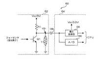
次に、図4を参照して、第1基板に設けられたフォトセンサ35と、第2基板に設けられたCPU40との間を電気的に接続する、本実施の形態に係る接続回路60の構成を説明する。 Next, referring to FIG. 4, the
同図に示すように、本実施の形態に係る接続回路60は、前述した第1基板62に設けられ、ベースがフォトセンサ35における受光素子の出力端子に電気的に接続されたトランジスタQ1が備えられている。ここで、トランジスタQ1のコレクタは抵抗器R1を介して予め定められた電圧(本実施の形態では、5V)にプル・アップされる一方、トランジスタQ1のエミッタは接地されている。 As shown in the figure, the
一方、本実施の形態に係る接続回路60は、前述した第2基板64に設けられ、入力された電圧の上限値を予め定められた電圧値に制限するように変換して出力する電圧変換部66が備えられている。なお、本実施の形態に係る電圧変換部66は、図5に示すように、抵抗器R2およびツェナー・ダイオードZ1により構成されたクリップ回路により構成されている。本実施の形態に係る電圧変換部66では、ツェナー・ダイオードZ1として、ツェナー電圧Vzが3.3Vのものを適用している。従って、本実施の形態に係る電圧変換部66では、入力電圧が3.3Vを超える場合に出力電圧を3.3Vに降圧する。 On the other hand, the
また、トランジスタQ1のコレクタはケーブルCBLを介して電圧変換部66の入力端子に接続されており、電圧変換部66の出力端子はCPU40に接続されている。このように、本実施の形態に係る接続回路60では、トランジスタQ1によってオープン・コレクタ回路を構成している。 The collector of the transistor Q1 is connected to the input terminal of the
ここで、本実施の形態に係る接続回路60には、設けられた位置の温度を検出する温度検出手段としてのNTC型のサーミスタT1が備えられており、サーミスタT1の一方の端子はトランジスタQ1のコレクタに接続される一方、他方の端子は接地されている。なお、図2に示されるように、本実施の形態に係る画像形成装置10では、サーミスタT1がフォトセンサ35に一体的に設けられている。 Here, the
一方、第2基板64において電圧変換部66の入力端子は分岐されてA/D変換器68の入力端子に接続されており、A/D変換器68の出力端子はCPU40に接続されている。 On the other hand, in the
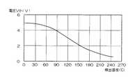
本実施の形態に係る接続回路60では、サーミスタT1として、基準抵抗値が10kΩ、基準温度が25°C、B定数が4000の定格のものを適用しており、サーミスタT1により検出される温度が異常であるときの下限温度(以下、「異常下限温度」という。)を120°Cとし、当該異常下限温度を中心としてサーミスタT1のリニアライズを行う。 In the
図6には、上記リニアライズするためのプル・アップ抵抗として抵抗器R1の抵抗値を200ΩとしたときのサーミスタT1による検出温度に対するサーミスタT1の出力電圧Vthが示されている。 FIG. 6 shows the output voltage Vth of the thermistor T1 with respect to the temperature detected by the thermistor T1 when the resistance value of the resistor R1 is 200Ω as the pull-up resistor for linearization.
同図に示すように、この場合、サーミスタT1による検出温度が異常下限温度(120°C)のときの出力電圧Vthは約3.3Vとなり、検出温度が0°Cから120°Cまでの範囲内、すなわち正常時における温度範囲(以下、「正常温度範囲」という。)内であるときの出力電圧Vthは5Vから3.3Vまでの範囲内に収まる。従って、検出温度が正常温度範囲内にあるときは、出力電圧Vthが電圧変換部66によって3.3Vにクリップされるので、CPU40は、電圧変換部66から入力された信号を、フォトセンサ35から出力され、ハイ・レベル(High Level)が3.3Vとされた2値を示す通過検出信号として取り扱う。 As shown in the figure, in this case, when the temperature detected by the thermistor T1 is the abnormal lower limit temperature (120 ° C), the output voltage Vth is about 3.3V, and the detected temperature ranges from 0 ° C to 120 ° C. Output voltage Vth within the normal temperature range (hereinafter referred to as “normal temperature range”) falls within the range from 5V to 3.3V. Accordingly, when the detected temperature is within the normal temperature range, the output voltage Vth is clipped to 3.3 V by the
図7(A)には、画像形成動作時においてサーミスタT1による検出温度が徐々に上昇した場合における、当該検出温度と出力電圧Vthとの関係の一例を示すグラフが示されている。 FIG. 7A shows a graph showing an example of the relationship between the detected temperature and the output voltage Vth when the temperature detected by the thermistor T1 gradually increases during the image forming operation.
同図に示すように、出力電圧Vthはフォトセンサ35による検出結果を示す2値出力のハイ・レベルに対して検出温度に応じた電圧が重畳された状態となる。このため、CPU40は、A/D変換器68から出力された電圧レベルを示す値を参照することによって、サーミスタT1により検出された温度を把握する。 As shown in the figure, the output voltage Vth is in a state in which a voltage corresponding to the detected temperature is superimposed on the high level of the binary output indicating the detection result by the
なお、図7(B)には、画像形成動作時においてサーミスタT1による検出温度の上昇が図7(A)に示されるものである場合の電圧変換部66の出力電圧が示されている。同図からも明らかなように、検出温度が正常温度範囲内にあるときは、3.3Vから5Vまでの範囲内の出力電圧Vthが電圧変換部66によって3.3Vにクリップされる結果、CPU40は、電圧変換部66から入力された信号を、フォトセンサ35から出力された2値を示す通過検出信号として取り扱う点は前述した通りである。そして、CPU40は、電圧変換部66から得られた通過検出信号に基づいて、画像形成エンジン部15による画像形成動作を、画像形成エンジン制御部54を介して制御する。 FIG. 7B shows the output voltage of the
ところで、本実施の形態に係る画像形成装置10では、サーミスタT1によって検出された温度が異常である場合に当該異常に対処する異常対処処理を実行する異常温度対応機能が搭載されている。 By the way, in the
なお、一例として図8に示すように、フォトセンサ35からの出力電圧Voltは、画像形成動作時には用紙31の検出状態に応じて頻繁に変化するため、サーミスタT1による検出温度を把握することが難しい。そこで、本実施の形態に係る画像形成装置10では、出力電圧Voltが殆ど変化しない、スタンバイ・モード、スリープ・モード等の省電力モードに移行している期間や、一連の画像形成動作が終了した時点から次の画像形成動作が開始されるまでの期間等の非画像形成期間に異常温度対応機能が実行される。 As an example, as shown in FIG. 8, the output voltage Volt from the photosensor 35 frequently changes according to the detection state of the
次に、図9を参照して、異常温度対応機能が実行される際の本実施の形態に係る画像形成装置10の作用を説明する。なお、図9は、上記非画像形成期間にCPU40によって実行される異常温度対応処理プログラムの処理の流れを示すフローチャートであり、当該プログラムはROM42に予め記憶されている。 Next, with reference to FIG. 9, the operation of the
同図のステップ100では、A/D変換器68からの出力値を取得することによりサーミスタT1による検出温度T1を取得する。なお、A/D変換器68から取得される出力値はサーミスタT1による出力電圧Vthの電圧レベルを示す値となっているため、CPU40は、予め定められた変換情報(一例として、図6に示される出力電圧Vthと検出温度との関係を示す情報)に基づいて、A/D変換器68から取得した出力値を検出温度T1に変換する。 In
次のステップ102では、検出温度T1が上記異常下限温度(本実施の形態では、120°C)より高いか否かを判定し、否定判定となった場合は後述するステップ116に移行する一方、肯定判定となった場合にはステップ104に移行する。 In the
ステップ104では、検出温度T1をフラッシュメモリ43に記憶し、次のステップ106にて、サーミスタT1による検出温度の上昇速度を導出する際のインターバルとして予め定められた期間(本実施の形態では、10秒間)の経過待ちを行う。 In
次のステップ108では、この時点のサーミスタT1による検出温度T2を上記ステップ100と同様に取得し、次のステップ110にて、検出温度T2から検出温度T1を減算することによって上記予め定められた期間当たりの上昇温度(以下、「温度上昇速度」という。)Sを算出する。 In the
次のステップ112では、温度上昇速度Sが予め定められた速度閾値Sth以上であるか否かを判定し、否定判定となった場合は後述するステップ116に移行する一方、肯定判定となった場合にはステップ114に移行する。なお、上記ステップ112において適用する速度閾値Sthは、サーミスタT1による検出温度が異常に速く上昇していることを検出するための閾値であり、予め固定的に保持しておいてもよく、画像形成装置10の設置環境や画像形成装置10の使用頻度等に応じて、ユーザによりディスプレイ14等の受付手段を介して設定するようにしてもよい。 In the next step 112, it is determined whether or not the temperature rise speed S is equal to or higher than a predetermined speed threshold Sth. If the determination is negative, the process proceeds to step 116 described later, whereas the determination is affirmative. Then, the process proceeds to step 114. Note that the speed threshold value Sth applied in step 112 is a threshold value for detecting that the temperature detected by the thermistor T1 is rising abnormally fast, and may be held in a fixed manner in advance. Depending on the installation environment of the
ステップ114では、予め定められた異常対処処理を実行し、その後にステップ116に移行する。なお、本実施の形態に係る画像形成装置10では、上記異常対処処理として、異常の発生をディスプレイ14等の表示手段や外部装置等を介して報知する処理、および異常の発生をフラッシュメモリ43等の記憶手段に記憶する処理を適用しているが、これに限らず、これらの処理に加えて、何らかの画像形成動作が実行されている場合の当該動作を強制的に停止させる処理等の、異常温度に対処する予め定められた処理の1つ、または複数の組み合わせを適用してもよい。 In
ステップ116では、本異常温度対応処理プログラムを終了するタイミングとして予め定められたタイミングが到来したか否かを判定し、否定判定となった場合は上記ステップ100に戻る一方、肯定判定となった時点で本異常温度対応処理プログラムを終了する。なお、本実施の形態に係る画像形成装置10では、上記予め定められたタイミングとして、上記非画像形成期間が終了したタイミングを適用しているが、これに限らず、このタイミングに加えて、ユーザによって画像形成装置10のメイン・スイッチがオフされたタイミング、ユーザからの異常温度対応処理プログラムの停止を指示する指示入力がディスプレイ14等の受付手段を介して受け付けられたタイミング等の1つ、または複数の組み合わせを適用してもよい。 In step 116, it is determined whether or not a predetermined timing has arrived as a timing for ending the abnormal temperature handling processing program. If a negative determination is made, the process returns to step 100, while a positive determination is made. Then, the abnormal temperature response processing program is terminated. In the
[第2の実施の形態]
上記第1の実施の形態では、オープン・コレクタ回路による2値出力のハイ・レベルにサーミスタT1からの出力を重畳させる場合の形態例について説明したが、本第2の実施の形態では、オープン・コレクタ回路による2値出力のロー・レベル(Low Level)にサーミスタT1からの出力を重畳させる場合の形態例について説明する。なお、本第2の実施の形態に係る画像形成装置の構成は、上記第1の実施の形態に係る画像形成装置10(図1〜図3参照。)と同様であるので、ここでの説明は省略する。[Second Embodiment]
In the first embodiment, an example in which the output from the thermistor T1 is superimposed on the high level of the binary output by the open collector circuit has been described. However, in the second embodiment, the open An example of a case in which the output from the thermistor T1 is superimposed on the low level of the binary output by the collector circuit will be described. The configuration of the image forming apparatus according to the second embodiment is the same as that of the image forming apparatus 10 (see FIGS. 1 to 3) according to the first embodiment, and will be described here. Is omitted.
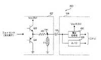
以下、図10を参照して、第1基板62に設けられたフォトセンサ35と、第2基板64に設けられたCPU40との間を電気的に接続する、本第2の実施の形態に係る接続回路60’の構成を説明する。 Hereinafter, referring to FIG. 10, according to the second embodiment, the photosensor 35 provided on the
同図に示すように、本第2の実施の形態に係る接続回路60’は、第1基板62に設けられ、ベースがフォトセンサ35における受光素子の出力端子に電気的に接続されたトランジスタQ2が備えられている。ここで、トランジスタQ2のコレクタは抵抗器R3を介して予め定められた電圧(本実施の形態では、5V)にプル・アップされている。 As shown in the figure, the
一方、本第2の実施の形態に係る接続回路60’は、第2基板64に設けられ、入力された電圧の下限値を予め定められた電圧値に制限するように変換して出力する電圧変換部70が備えられている。なお、本実施の形態に係る電圧変換部70は、同図に示すように、コンデンサC1およびダイオードD1により構成されたクランプ回路により構成されている。 On the other hand, the
また、トランジスタQ2のコレクタはケーブルCBLを介して電圧変換部70の入力端子に接続されており、電圧変換部70の出力端子はCPU40に接続されている。このように、本第2の実施の形態に係る接続回路60’でも、トランジスタQ2によってオープン・コレクタ回路を構成している。 The collector of the transistor Q2 is connected to the input terminal of the
ここで、本第2の実施の形態に係る接続回路60’では、フォトセンサ35に一体的に設けられたサーミスタT2の一方の端子がトランジスタQ2のエミッタに接続される一方、他方の端子は接地されている。また、トランジスタQ2のエミッタは抵抗器R4を介して接地されている。 Here, in the
一方、第2基板64において電圧変換部70の入力端子は分岐されてA/D変換器72の入力端子に接続されており、A/D変換器72の出力端子はCPU40に接続されている。 On the other hand, in the
図11(A)には、画像形成動作時においてサーミスタT2による検出温度が徐々に上昇した場合における、当該検出温度と図10に示される出力電圧Vthとの関係の一例を示すグラフが示されている。 FIG. 11A shows a graph showing an example of the relationship between the detected temperature and the output voltage Vth shown in FIG. 10 when the temperature detected by the thermistor T2 gradually increases during the image forming operation. Yes.
同図に示すように、本第2の実施の形態に係る接続回路60’においては、出力電圧Vthがフォトセンサ35による検出結果を示す2値出力のロー・レベル側に対してサーミスタT2による検出温度に応じた電圧が重畳された状態となる。このため、CPU40は、A/D変換器72から出力された電圧レベルを示す値を参照することによって、サーミスタT2により検出された温度を把握する。 As shown in the figure, in the
なお、図11(B)には、画像形成動作時においてサーミスタT2による検出温度の上昇が図11(A)に示されるものである場合の電圧変換部70の出力電圧が示されている。同図からも明らかなように、出力電圧Vthのロー・レベルが電圧変換部70によって0Vにクランプされる結果、CPU40は、電圧変換部70から入力された信号を、フォトセンサ35から出力された2値を示す通過検出信号として取り扱う。そして、CPU40は、電圧変換部70から得られた通過検出信号に基づいて、画像形成エンジン部15による画像形成動作を、画像形成エンジン制御部54を介して制御する。 FIG. 11B shows the output voltage of the
なお、本第2の実施の形態に係る画像形成装置10においても、図9に示した異常温度対応処理プログラムが上記第1の実施の形態と同じタイミングでCPU40により実行されるが、この説明については省略する。 In the
以上詳細に説明したように、上記各実施の形態では、画像形成動作に関する予め定められた検出対象を検出する検出手段(ここでは、フォトセンサ35)と、装置筐体内の予め定められた位置に設けられ、設けられた位置の温度を検出する温度検出手段(ここでは、サーミスタT1)と、前記検出手段による検出結果を示す信号および前記温度検出手段による検出結果を示す信号が重畳されて伝送されるように前記検出手段と前記温度検出手段とに接続された接続配線(ここでは、ケーブルCBL)と、を備え、前記接続配線により伝送された信号が入力されるように前記接続配線に接続された制御手段(ここでは、CPU40)により、当該接続配線により伝送された信号により示される前記検出手段による検出結果に基づいて前記画像形成動作を制御すると共に、前記接続配線により伝送された信号により示される前記温度検出手段により検出された温度が異常である場合に当該異常に対処する異常対処制御を行っている。 As described above in detail, in each of the above-described embodiments, the detection means (here, the photosensor 35) for detecting a predetermined detection target related to the image forming operation, and the predetermined position in the apparatus housing are provided. The temperature detection means (here, the thermistor T1) that is provided and detects the temperature at the provided position, the signal indicating the detection result by the detection means, and the signal indicating the detection result by the temperature detection means are superimposed and transmitted. A connection wiring (here, cable CBL) connected to the detection means and the temperature detection means, and connected to the connection wiring so that a signal transmitted by the connection wiring is input. On the basis of the detection result by the detection means indicated by the signal transmitted by the connection wiring by the control means (here, the CPU 40), the image shape It controls the operation is performed the abnormality abnormality handling control to deal with when the temperature detected by said temperature detecting means is indicated by the signal transmitted is abnormal by the connection wiring.
以上、本発明を上記実施の形態を用いて説明したが、本発明の技術的範囲は上記実施の形態に記載の範囲には限定されない。発明の主旨を逸脱しない範囲で上記実施の形態に多様な変更または改良を加えることができ、当該変更または改良を加えた形態も本発明の技術的範囲に含まれる。 As mentioned above, although this invention was demonstrated using the said embodiment, the technical scope of this invention is not limited to the range as described in the said embodiment. Various changes or improvements can be added to the above-described embodiment without departing from the gist of the invention, and embodiments to which the changes or improvements are added are also included in the technical scope of the present invention.
また、上記実施の形態は、特許請求の範囲に記載された発明を限定するものではなく、また、上記実施の形態の中で説明されている特徴の組み合わせの全てが発明の解決手段に必須であるとは限らない。上記実施の形態には種々の段階の発明が含まれており、開示される複数の構成要件における状況に応じた組み合わせにより種々の発明が抽出される。上記実施の形態に示される全構成要件から幾つかの構成要件が削除されても、効果が得られる限りにおいて、この幾つかの構成要件が削除された構成が発明として抽出される。 The above embodiments do not limit the invention described in the claims, and all combinations of features described in the above embodiments are indispensable for the solution means of the invention. Not always. The above-described embodiments include inventions at various stages, and various inventions are extracted by combinations according to situations in a plurality of disclosed constituent requirements. Even if some constituent features are deleted from all the constituent features shown in the above embodiment, the configuration from which these constituent features are deleted is extracted as an invention as long as the effect is obtained.
例えば、上記各実施の形態では、接続回路にオープン・コレクタ回路を適用した場合について説明したが、本発明はこれに限定されるものではなく、例えば、一例として図12に示すようなトーテムポール出力回路を接続回路に適用する形態としてもよい。なお、同図における図4と同一の構成要素には図4と同一の符号が付してある。 For example, in each of the above embodiments, the case where an open collector circuit is applied to the connection circuit has been described. However, the present invention is not limited to this, and for example, a totem pole output as shown in FIG. The circuit may be applied to the connection circuit. In addition, the same code | symbol as FIG. 4 is attached | subjected to the component same as FIG. 4 in the same figure.
また、上記各実施の形態では、錯綜を回避するために、本発明を1つのみのセンサ出力(上記各実施の形態では、フォトセンサ35の出力)を伝送する接続回路に適用した場合について説明したが、本発明はこれに限定されるものではなく、複数のセンサ出力に適用する形態としてもよいことは言うまでもない。画像形成装置には、一般に、多数の用紙検出用のセンサが用紙の搬送経路上に分散して設けられているため、これらのセンサに対して上記各実施の形態に係る接続回路と同様の構成を採用することにより、接続配線数の増加の抑制効果が、より多く享受される。 Further, in each of the above embodiments, in order to avoid complications, the case where the present invention is applied to a connection circuit that transmits only one sensor output (the output of the photosensor 35 in each of the above embodiments) will be described. However, it is needless to say that the present invention is not limited to this, and may be applied to a plurality of sensor outputs. In general, an image forming apparatus is provided with a large number of paper detection sensors distributed on a paper transport path. Therefore, the same configuration as the connection circuit according to each of the above embodiments is provided for these sensors. By adopting, the effect of suppressing the increase in the number of connection wirings can be enjoyed more.
また、上記各実施の形態では、接続回路60および接続回路60’で用いるトランジスタとしてバイポーラ・トランジスタを適用した場合について説明したが、本発明はこれに限定されるものではなく、例えば、電界効果トランジスタを適用する形態としてもよい。なお、この場合、上記各実施の形態におけるオープン・コレクタ回路に代えてオープン・ドレイン回路が適用されることになる。 In each of the above embodiments, the case where a bipolar transistor is applied as the transistor used in the
また、上記各実施の形態では、本発明の検出手段による検出対象として用紙31の通過状態を適用した場合について説明したが、本発明はこれに限定されるものではなく、例えば、用紙31の紙詰まり、現像器28におけるトナー残量、給紙トレイにおける用紙残量等、他の検出対象を適用する形態としてもよい。 In each of the above embodiments, the case where the passage state of the
また、上記各実施の形態では、異常温度対応処理プログラムにおいてサーミスタT1による検出温度が異常下限温度より高く、かつ当該検出温度の温度上昇速度が速度閾値Sth以上である場合に異常対処処理を実行する場合について説明したが、本発明はこれに限定されるものではなく、上記検出温度が異常下限温度より高い場合に異常対処処理を実行する形態や、上記温度上昇速度が速度閾値Sth以上である場合に異常対処処理を実行する形態としてもよい。 In each of the above embodiments, the abnormality handling process is executed when the temperature detected by the thermistor T1 is higher than the abnormality lower limit temperature and the temperature rise rate of the detected temperature is equal to or higher than the speed threshold Sth in the abnormality temperature handling processing program. Although the case has been described, the present invention is not limited to this, and a mode in which an abnormality handling process is executed when the detected temperature is higher than the abnormal lower limit temperature, or the temperature increase rate is equal to or higher than the speed threshold Sth. Alternatively, the abnormality handling process may be executed.
また、上記各実施の形態では、非画像形成時に異常温度対応処理プログラムを実行する場合について説明したが、本発明はこれに限定されるものではなく、画像形成時に実行する形態や、画像形成時および非画像形成時の双方で実行する形態としてもよい。 In each of the above-described embodiments, the case where the abnormal temperature response processing program is executed at the time of non-image formation has been described. However, the present invention is not limited to this. It is also possible to execute both at the time of image formation and during non-image formation.
また、上記各実施の形態では、本発明の画像形成装置を、電子写真方式により画像を形成する画像形成装置に適用した場合について説明したが、本発明はこれに限定されるものではなく、例えば、液滴吐出装置(所謂インクジェットプリンタ)等の他の画像形成装置に本発明の画像形成装置を適用する形態としてもよい。 In each of the above embodiments, the case where the image forming apparatus of the present invention is applied to an image forming apparatus that forms an image by an electrophotographic method has been described. However, the present invention is not limited to this, for example, The image forming apparatus of the present invention may be applied to other image forming apparatuses such as a droplet discharge apparatus (so-called inkjet printer).
また、上記各実施の形態では、異常温度対応処理プログラムがROM42に予め記憶されている場合について説明したが、本発明はこれに限定されるものではなく、当該プログラムをCD−ROMやDVD−ROM、USBメモリなどのコンピュータ読み取り可能な記録媒体に格納した状態で提供する形態を適用してもよいし、有線又は無線による通信手段を介して配信する形態を適用してもよい。 In each of the above-described embodiments, the case where the abnormal temperature response processing program is stored in advance in the
また、上記各実施の形態では、本発明の温度検出手段として、NTC型のサーミスタを適用した場合について説明したが、本発明はこれに限定されるものではなく、例えば、PTC型,CTR型等の他のサーミスタや、熱電対、バイメタル、測温抵抗体等の他の温度センサを適用してもよい。 In each of the above embodiments, the case where an NTC type thermistor is applied as the temperature detecting means of the present invention has been described. However, the present invention is not limited to this, for example, PTC type, CTR type, etc. Other temperature sensors such as other thermistors, thermocouples, bimetals, and resistance temperature detectors may be applied.
その他、上記各実施の形態で説明した画像形成装置の構成(図1〜図3参照。)は一例であり、本発明の主旨を逸脱しない範囲内において、不要な部位を削除したり、新たな部位を追加したり、各部位の配設位置を変更したりしてもよい。 In addition, the configuration of the image forming apparatus described in each of the above embodiments (see FIGS. 1 to 3) is merely an example, and unnecessary portions may be deleted or new ones may be used without departing from the gist of the present invention. A part may be added or the arrangement position of each part may be changed.
また、上記各実施の形態で説明した接続回路の構成(図4,図10参照。)は一例であり、本発明の主旨を逸脱しない範囲内において、不要な部位を削除したり、新たな部位を追加したり、各部位の配設位置を変更したりしてもよい。 In addition, the configuration of the connection circuit (see FIGS. 4 and 10) described in each of the above embodiments is an example, and unnecessary parts can be deleted or new parts can be used without departing from the gist of the present invention. May be added, or the arrangement position of each part may be changed.
さらに、上記各実施の形態で説明した異常温度対応処理プログラムの処理の流れ(図9参照。)も一例であり、本発明の主旨を逸脱しない範囲内において不要なステップを削除したり、新たなステップを追加したり、処理順序を入れ替えたりしてもよい。 Furthermore, the processing flow of the abnormal temperature response processing program described in each of the above embodiments (see FIG. 9) is also an example, and unnecessary steps can be deleted or new within the scope of the present invention. Steps may be added or the processing order may be changed.
10 画像形成装置
15 画像形成エンジン部
31 用紙(記録媒体)
35 フォトセンサ(検出手段)
40 CPU(制御手段)
42 ROM
60,60’,60’’ 接続回路
62 第1基板
64 第2基板
66 電圧変換部
68 A/D変換器
70 電圧変換部
72 A/D変換器
C1 コンデンサ
CBL ケーブル(接続配線)
D1 ダイオード
Q1〜Q4 トランジスタ
R1〜R5 抵抗器
T1,T2 サーミスタ(温度検出手段)
Z1 ツェナー・ダイオードDESCRIPTION OF
35 Photosensor (detection means)
40 CPU (control means)
42 ROM
60, 60 ′, 60 ″
D1 Diodes Q1 to Q4 Transistors R1 to R5 Resistors T1, T2 Thermistor (temperature detection means)
Z1 Zener diode
Claims (9)
Translated fromJapanese装置筐体内の予め定められた位置に設けられ、設けられた位置の温度を検出する温度検出手段と、
前記検出手段による検出結果を示す信号および前記温度検出手段による検出結果を示す信号が重畳されて伝送されるように前記検出手段と前記温度検出手段とに接続された接続配線と、
前記接続配線により伝送された信号が入力されるように前記接続配線に接続され、当該接続配線により伝送された信号により示される前記検出手段による検出結果に基づいて前記画像形成動作を制御すると共に、前記接続配線により伝送された信号により示される前記温度検出手段により検出された温度が異常である場合に当該異常に対処する異常対処制御を行う制御手段と、
を備えた画像形成装置。Detecting means for detecting a predetermined detection object relating to the image forming operation;
A temperature detecting means provided at a predetermined position in the apparatus housing and detecting a temperature at the provided position;
A connection wiring connected to the detection unit and the temperature detection unit so that a signal indicating the detection result by the detection unit and a signal indicating the detection result by the temperature detection unit are transmitted in a superimposed manner;
While being connected to the connection wiring so that a signal transmitted by the connection wiring is input, and controlling the image forming operation based on the detection result by the detection means indicated by the signal transmitted by the connection wiring, Control means for performing abnormality handling control for dealing with the abnormality when the temperature detected by the temperature detection means indicated by the signal transmitted by the connection wiring is abnormal;
An image forming apparatus.
請求項1記載の画像形成装置。The image forming apparatus according to claim 1, wherein the connection wiring is connected to the detection unit and the temperature detection unit via an open collector circuit or an open drain circuit.
前記予め定められた検出対象は、搬送されている前記記録媒体の先端位置、搬送されている前記記録媒体の後端位置、および前記記録媒体の搬送経路上での詰まり状態の少なくとも1つである
請求項1または請求項2記載の画像形成装置。The image forming operation is an operation of forming an image on the recording medium in a state where the recording medium is conveyed,
The predetermined detection target is at least one of a leading end position of the recording medium being transported, a trailing end position of the recording medium being transported, and a clogged state on the transport path of the recording medium. The image forming apparatus according to claim 1.
請求項1〜請求項3の何れか1項記載の画像形成装置。The abnormality handling control is at least one of a control for notifying the occurrence of an abnormality, a control for stopping an image forming operation, and a control for recording the occurrence of an abnormality. Image forming apparatus.
請求項1〜請求項4の何れか1項記載の画像形成装置。The control unit performs the abnormality handling control when the temperature indicated by the signal transmitted by the connection wiring is abnormal when the image forming operation is stopped. The image forming apparatus according to claim 1.
請求項1〜請求項5の何れか1項記載の画像形成装置。6. The image formation according to claim 1, wherein the control unit performs the abnormality handling control when the temperature indicated by a signal transmitted through the connection wiring is higher than a predetermined threshold value. apparatus.
請求項1〜請求項6の何れか1項記載の画像形成装置。The said control means performs the said abnormality countermeasure control when the rate of temperature rise shown by the signal transmitted by the said connection wiring is faster than a predetermined threshold value. Image forming apparatus.
請求項1〜請求項7の何れか1項記載の画像形成装置。The image forming apparatus according to claim 1, wherein the detection unit and the temperature detection unit are integrally configured.
Priority Applications (1)
| Application Number | Priority Date | Filing Date | Title |
|---|---|---|---|
| JP2009058147AJP2010208200A (en) | 2009-03-11 | 2009-03-11 | Image forming device and program |
Applications Claiming Priority (1)
| Application Number | Priority Date | Filing Date | Title |
|---|---|---|---|
| JP2009058147AJP2010208200A (en) | 2009-03-11 | 2009-03-11 | Image forming device and program |
Publications (1)
| Publication Number | Publication Date |
|---|---|
| JP2010208200Atrue JP2010208200A (en) | 2010-09-24 |
Family
ID=42968908
Family Applications (1)
| Application Number | Title | Priority Date | Filing Date |
|---|---|---|---|
| JP2009058147APendingJP2010208200A (en) | 2009-03-11 | 2009-03-11 | Image forming device and program |
Country Status (1)
| Country | Link |
|---|---|
| JP (1) | JP2010208200A (en) |
Cited By (1)
| Publication number | Priority date | Publication date | Assignee | Title |
|---|---|---|---|---|
| KR20170084306A (en)* | 2014-12-31 | 2017-07-19 | 후아웨이 테크놀러지 컴퍼니 리미티드 | Charging protection method and apparatus |
- 2009
- 2009-03-11JPJP2009058147Apatent/JP2010208200A/enactivePending
Cited By (5)
| Publication number | Priority date | Publication date | Assignee | Title |
|---|---|---|---|---|
| KR20170084306A (en)* | 2014-12-31 | 2017-07-19 | 후아웨이 테크놀러지 컴퍼니 리미티드 | Charging protection method and apparatus |
| JP2018501762A (en)* | 2014-12-31 | 2018-01-18 | 華為技術有限公司Huawei Technologies Co.,Ltd. | Charge protection method and apparatus |
| US10250048B2 (en) | 2014-12-31 | 2019-04-02 | Huawei Technologies Co., Ltd. | Charging protection method and apparatus |
| KR102085684B1 (en)* | 2014-12-31 | 2020-03-06 | 후아웨이 테크놀러지 컴퍼니 리미티드 | Charging protection method and apparatus |
| US10778018B2 (en) | 2014-12-31 | 2020-09-15 | Huawei Technologies Co., Ltd. | Charging protection method and apparatus |
Similar Documents
| Publication | Publication Date | Title |
|---|---|---|
| KR20120083764A (en) | Apparatus and method for protecting fusing unit in image forming apparatus, and image forming apparatus having it | |
| JP2009293942A (en) | Humidity detector and image-forming device having the same | |
| KR101776930B1 (en) | Image forming apparatus and control method thereof | |
| JP4462375B2 (en) | Image forming apparatus and fixing apparatus | |
| JP2008102413A (en) | Fixing device | |
| JP2010208200A (en) | Image forming device and program | |
| JP6106581B2 (en) | Image forming apparatus | |
| KR20130031017A (en) | Protection apparatus for fuser, and image forming apparatus having it | |
| JP2010113237A (en) | Image forming apparatus and program | |
| JP6097709B2 (en) | Paper feed control device and image forming apparatus | |
| JP2015208890A (en) | Image formation apparatus | |
| JP6364966B2 (en) | Image forming apparatus, sheet conveying method, and program | |
| JP2007003992A (en) | Image forming apparatus | |
| US8175472B2 (en) | Image forming apparatus | |
| JP5340117B2 (en) | Image forming apparatus having fan | |
| JP6841065B2 (en) | Fixing device, image forming device, abnormality occurrence judgment device, and program | |
| JP2008026201A (en) | Disconnection detector and image forming device | |
| JP2008236940A (en) | Image forming apparatus | |
| JP2009093085A (en) | Fixing apparatus and image forming apparatus | |
| JP2003345166A (en) | Image forming device | |
| JP5927156B2 (en) | Image forming apparatus | |
| JP2009069558A (en) | Image forming apparatus | |
| JP4948309B2 (en) | Connector connection detector | |
| JP2007003564A (en) | Printing device | |
| JP2008083103A (en) | Image forming apparatus |