JP2010204633A - Liquid crystal display, manufacturing method of liquid crystal display, display device and information input apparatus - Google Patents
Liquid crystal display, manufacturing method of liquid crystal display, display device and information input apparatusDownload PDFInfo
- Publication number
- JP2010204633A JP2010204633AJP2009265486AJP2009265486AJP2010204633AJP 2010204633 AJP2010204633 AJP 2010204633AJP 2009265486 AJP2009265486 AJP 2009265486AJP 2009265486 AJP2009265486 AJP 2009265486AJP 2010204633 AJP2010204633 AJP 2010204633A
- Authority
- JP
- Japan
- Prior art keywords
- substrate
- liquid crystal
- touch electrode
- touch
- facing
- Prior art date
- Legal status (The legal status is an assumption and is not a legal conclusion. Google has not performed a legal analysis and makes no representation as to the accuracy of the status listed.)
- Granted
Links
Images


Classifications
- G—PHYSICS
- G02—OPTICS
- G02F—OPTICAL DEVICES OR ARRANGEMENTS FOR THE CONTROL OF LIGHT BY MODIFICATION OF THE OPTICAL PROPERTIES OF THE MEDIA OF THE ELEMENTS INVOLVED THEREIN; NON-LINEAR OPTICS; FREQUENCY-CHANGING OF LIGHT; OPTICAL LOGIC ELEMENTS; OPTICAL ANALOGUE/DIGITAL CONVERTERS
- G02F1/00—Devices or arrangements for the control of the intensity, colour, phase, polarisation or direction of light arriving from an independent light source, e.g. switching, gating or modulating; Non-linear optics
- G02F1/01—Devices or arrangements for the control of the intensity, colour, phase, polarisation or direction of light arriving from an independent light source, e.g. switching, gating or modulating; Non-linear optics for the control of the intensity, phase, polarisation or colour
- G02F1/13—Devices or arrangements for the control of the intensity, colour, phase, polarisation or direction of light arriving from an independent light source, e.g. switching, gating or modulating; Non-linear optics for the control of the intensity, phase, polarisation or colour based on liquid crystals, e.g. single liquid crystal display cells
- G02F1/133—Constructional arrangements; Operation of liquid crystal cells; Circuit arrangements
- G02F1/1333—Constructional arrangements; Manufacturing methods
- G02F1/13338—Input devices, e.g. touch panels
- G—PHYSICS
- G06—COMPUTING OR CALCULATING; COUNTING
- G06F—ELECTRIC DIGITAL DATA PROCESSING
- G06F3/00—Input arrangements for transferring data to be processed into a form capable of being handled by the computer; Output arrangements for transferring data from processing unit to output unit, e.g. interface arrangements
- G06F3/01—Input arrangements or combined input and output arrangements for interaction between user and computer
- G06F3/03—Arrangements for converting the position or the displacement of a member into a coded form
- G06F3/041—Digitisers, e.g. for touch screens or touch pads, characterised by the transducing means
- G06F3/0412—Digitisers structurally integrated in a display
- G—PHYSICS
- G06—COMPUTING OR CALCULATING; COUNTING
- G06F—ELECTRIC DIGITAL DATA PROCESSING
- G06F3/00—Input arrangements for transferring data to be processed into a form capable of being handled by the computer; Output arrangements for transferring data from processing unit to output unit, e.g. interface arrangements
- G06F3/01—Input arrangements or combined input and output arrangements for interaction between user and computer
- G06F3/03—Arrangements for converting the position or the displacement of a member into a coded form
- G06F3/041—Digitisers, e.g. for touch screens or touch pads, characterised by the transducing means
- G06F3/047—Digitisers, e.g. for touch screens or touch pads, characterised by the transducing means using sets of wires, e.g. crossed wires
- G—PHYSICS
- G02—OPTICS
- G02F—OPTICAL DEVICES OR ARRANGEMENTS FOR THE CONTROL OF LIGHT BY MODIFICATION OF THE OPTICAL PROPERTIES OF THE MEDIA OF THE ELEMENTS INVOLVED THEREIN; NON-LINEAR OPTICS; FREQUENCY-CHANGING OF LIGHT; OPTICAL LOGIC ELEMENTS; OPTICAL ANALOGUE/DIGITAL CONVERTERS
- G02F1/00—Devices or arrangements for the control of the intensity, colour, phase, polarisation or direction of light arriving from an independent light source, e.g. switching, gating or modulating; Non-linear optics
- G02F1/01—Devices or arrangements for the control of the intensity, colour, phase, polarisation or direction of light arriving from an independent light source, e.g. switching, gating or modulating; Non-linear optics for the control of the intensity, phase, polarisation or colour
- G02F1/13—Devices or arrangements for the control of the intensity, colour, phase, polarisation or direction of light arriving from an independent light source, e.g. switching, gating or modulating; Non-linear optics for the control of the intensity, phase, polarisation or colour based on liquid crystals, e.g. single liquid crystal display cells
- G02F1/133—Constructional arrangements; Operation of liquid crystal cells; Circuit arrangements
- G02F1/1333—Constructional arrangements; Manufacturing methods
- G02F1/1337—Surface-induced orientation of the liquid crystal molecules, e.g. by alignment layers
- G—PHYSICS
- G02—OPTICS
- G02F—OPTICAL DEVICES OR ARRANGEMENTS FOR THE CONTROL OF LIGHT BY MODIFICATION OF THE OPTICAL PROPERTIES OF THE MEDIA OF THE ELEMENTS INVOLVED THEREIN; NON-LINEAR OPTICS; FREQUENCY-CHANGING OF LIGHT; OPTICAL LOGIC ELEMENTS; OPTICAL ANALOGUE/DIGITAL CONVERTERS
- G02F1/00—Devices or arrangements for the control of the intensity, colour, phase, polarisation or direction of light arriving from an independent light source, e.g. switching, gating or modulating; Non-linear optics
- G02F1/01—Devices or arrangements for the control of the intensity, colour, phase, polarisation or direction of light arriving from an independent light source, e.g. switching, gating or modulating; Non-linear optics for the control of the intensity, phase, polarisation or colour
- G02F1/13—Devices or arrangements for the control of the intensity, colour, phase, polarisation or direction of light arriving from an independent light source, e.g. switching, gating or modulating; Non-linear optics for the control of the intensity, phase, polarisation or colour based on liquid crystals, e.g. single liquid crystal display cells
- G02F1/133—Constructional arrangements; Operation of liquid crystal cells; Circuit arrangements
- G02F1/1333—Constructional arrangements; Manufacturing methods
- G02F1/1339—Gaskets; Spacers; Sealing of cells
- G02F1/13394—Gaskets; Spacers; Sealing of cells spacers regularly patterned on the cell subtrate, e.g. walls, pillars
- G—PHYSICS
- G02—OPTICS
- G02F—OPTICAL DEVICES OR ARRANGEMENTS FOR THE CONTROL OF LIGHT BY MODIFICATION OF THE OPTICAL PROPERTIES OF THE MEDIA OF THE ELEMENTS INVOLVED THEREIN; NON-LINEAR OPTICS; FREQUENCY-CHANGING OF LIGHT; OPTICAL LOGIC ELEMENTS; OPTICAL ANALOGUE/DIGITAL CONVERTERS
- G02F1/00—Devices or arrangements for the control of the intensity, colour, phase, polarisation or direction of light arriving from an independent light source, e.g. switching, gating or modulating; Non-linear optics
- G02F1/01—Devices or arrangements for the control of the intensity, colour, phase, polarisation or direction of light arriving from an independent light source, e.g. switching, gating or modulating; Non-linear optics for the control of the intensity, phase, polarisation or colour
- G02F1/13—Devices or arrangements for the control of the intensity, colour, phase, polarisation or direction of light arriving from an independent light source, e.g. switching, gating or modulating; Non-linear optics for the control of the intensity, phase, polarisation or colour based on liquid crystals, e.g. single liquid crystal display cells
- G02F1/133—Constructional arrangements; Operation of liquid crystal cells; Circuit arrangements
- G02F1/1333—Constructional arrangements; Manufacturing methods
- G02F1/1343—Electrodes
- G02F1/134309—Electrodes characterised by their geometrical arrangement
- G02F1/134363—Electrodes characterised by their geometrical arrangement for applying an electric field parallel to the substrate, i.e. in-plane switching [IPS]
- G—PHYSICS
- G02—OPTICS
- G02F—OPTICAL DEVICES OR ARRANGEMENTS FOR THE CONTROL OF LIGHT BY MODIFICATION OF THE OPTICAL PROPERTIES OF THE MEDIA OF THE ELEMENTS INVOLVED THEREIN; NON-LINEAR OPTICS; FREQUENCY-CHANGING OF LIGHT; OPTICAL LOGIC ELEMENTS; OPTICAL ANALOGUE/DIGITAL CONVERTERS
- G02F1/00—Devices or arrangements for the control of the intensity, colour, phase, polarisation or direction of light arriving from an independent light source, e.g. switching, gating or modulating; Non-linear optics
- G02F1/01—Devices or arrangements for the control of the intensity, colour, phase, polarisation or direction of light arriving from an independent light source, e.g. switching, gating or modulating; Non-linear optics for the control of the intensity, phase, polarisation or colour
- G02F1/13—Devices or arrangements for the control of the intensity, colour, phase, polarisation or direction of light arriving from an independent light source, e.g. switching, gating or modulating; Non-linear optics for the control of the intensity, phase, polarisation or colour based on liquid crystals, e.g. single liquid crystal display cells
- G02F1/133—Constructional arrangements; Operation of liquid crystal cells; Circuit arrangements
- G02F1/1333—Constructional arrangements; Manufacturing methods
- G02F1/1343—Electrodes
- G02F1/134309—Electrodes characterised by their geometrical arrangement
- G02F1/134372—Electrodes characterised by their geometrical arrangement for fringe field switching [FFS] where the common electrode is not patterned
- G—PHYSICS
- G02—OPTICS
- G02F—OPTICAL DEVICES OR ARRANGEMENTS FOR THE CONTROL OF LIGHT BY MODIFICATION OF THE OPTICAL PROPERTIES OF THE MEDIA OF THE ELEMENTS INVOLVED THEREIN; NON-LINEAR OPTICS; FREQUENCY-CHANGING OF LIGHT; OPTICAL LOGIC ELEMENTS; OPTICAL ANALOGUE/DIGITAL CONVERTERS
- G02F2201/00—Constructional arrangements not provided for in groups G02F1/00 - G02F7/00
- G02F2201/40—Arrangements for improving the aperture ratio
Landscapes
- Engineering & Computer Science (AREA)
- Physics & Mathematics (AREA)
- Theoretical Computer Science (AREA)
- General Engineering & Computer Science (AREA)
- General Physics & Mathematics (AREA)
- Nonlinear Science (AREA)
- Human Computer Interaction (AREA)
- Mathematical Physics (AREA)
- Chemical & Material Sciences (AREA)
- Crystallography & Structural Chemistry (AREA)
- Optics & Photonics (AREA)
- Liquid Crystal (AREA)
- Position Input By Displaying (AREA)
Abstract
Description
Translated fromJapanese本発明は、液晶表示装置,液晶表示装置の製造方法,表示装置,情報入力装置に関する。特に、互いに対向する一対の基板にタッチセンサスイッチが設けられている、液晶表示装置,液晶表示装置の製造方法,表示装置,情報入力装置に関する。 The present invention relates to a liquid crystal display device, a method for manufacturing a liquid crystal display device, a display device, and an information input device. In particular, the present invention relates to a liquid crystal display device, a manufacturing method of a liquid crystal display device, a display device, and an information input device in which touch sensor switches are provided on a pair of substrates facing each other.
液晶表示装置,有機EL表示装置などの表示装置は、薄型、軽量、低消費電力といった利点を有する。このため、携帯電話、デジタルカメラなどのモバイル用途の電子機器にて多く使用されている。 Display devices such as liquid crystal display devices and organic EL display devices have advantages such as thinness, light weight, and low power consumption. For this reason, it is widely used in mobile electronic devices such as mobile phones and digital cameras.
このような表示装置において、液晶表示装置は、一対の基板の間に液晶層が封入された液晶パネルを、表示パネルとして有している。液晶パネルは、たとえば、透過型であって、液晶パネルの背面に設けられたバックライトなどの照明装置が出射した照明光を変調して透過させる。そして、その変調した照明光によって画像の表示が、液晶パネルの正面にて実施される。 In such a display device, the liquid crystal display device includes a liquid crystal panel in which a liquid crystal layer is sealed between a pair of substrates as a display panel. The liquid crystal panel is, for example, a transmission type, and modulates and transmits illumination light emitted from an illumination device such as a backlight provided on the back surface of the liquid crystal panel. An image is displayed on the front surface of the liquid crystal panel by the modulated illumination light.
この液晶パネルは、たとえば、アクティブマトリクス方式であり、画素スイッチング素子として機能する薄膜トランジスタ(TFT:Thin Film Transistor)が、複数形成されているTFTアレイ基板を含む。そして、液晶パネルにおいては、そのTFTアレイ基板に対向するように対向基板が配置されており、TFTアレイ基板および対向基板の間のスペースに液晶層が設けられている。このアクティブマトリクス方式の液晶パネルにおいては、画素スイッチング素子を介して画素電極に映像信号を入力することによって、液晶層に電圧を印加して、その画素を透過する光の透過率を制御することで、画像の表示が実施される。 This liquid crystal panel is, for example, an active matrix type, and includes a TFT array substrate on which a plurality of thin film transistors (TFTs) functioning as pixel switching elements are formed. In the liquid crystal panel, a counter substrate is disposed so as to face the TFT array substrate, and a liquid crystal layer is provided in a space between the TFT array substrate and the counter substrate. In this active matrix type liquid crystal panel, by inputting a video signal to the pixel electrode through the pixel switching element, a voltage is applied to the liquid crystal layer to control the transmittance of light transmitted through the pixel. The image is displayed.
上記のような表示装置においては、表示パネルの画面に表示されたアイコン等の画像を利用して、ユーザが操作データの入力を可能にするために、タッチパネルが情報入力装置として表示パネル上に設けられる場合がある。 In the display device as described above, a touch panel is provided on the display panel as an information input device so that a user can input operation data using an image such as an icon displayed on the screen of the display panel. May be.
しかし、表示パネル上にタッチパネルを外付けによって設置した場合には、全体の厚みが厚くなり、薄型の利点が損なわれる場合がある。また、タッチパネルによって、表示領域において透過する光が減少する場合や、その光が干渉される場合があるために、表示画像の品質が低下する場合がある。さらに、製造効率の低下や、製造コストの上昇などの不具合が生ずる場合がある。 However, when a touch panel is installed on the display panel by external attachment, the overall thickness is increased, and the advantage of thinness may be impaired. Further, since the light transmitted through the display area may be reduced or interfere with the touch panel, the quality of the display image may be deteriorated. Furthermore, problems such as a decrease in manufacturing efficiency and an increase in manufacturing cost may occur.
このため、タッチパネル機能が表示パネルに内蔵された表示装置が、提案されている。 For this reason, a display device in which a touch panel function is built in a display panel has been proposed.
たとえば、抵抗膜式のタッチセンサが液晶パネルに内蔵された液晶表示装置が提案されている。 For example, a liquid crystal display device in which a resistive touch sensor is built in a liquid crystal panel has been proposed.
ここでは、タッチセンサは、液晶パネルを構成する一対の基板のそれぞれにタッチ電極が設けられたタッチセンサスイッチを含み、液晶パネルが押されて変形したときに、その一対のタッチ電極が電気的に接続するように構成されている。この液晶パネルにおいては、両基板に形成されたタッチ電極が小さな外圧によって電気的に接続するように、凸状に突出している凸部上にタッチ電極が設けられている(たとえば、特許文献1、特許文献2、特許文献3参照)。 Here, the touch sensor includes a touch sensor switch in which a touch electrode is provided on each of a pair of substrates constituting the liquid crystal panel, and when the liquid crystal panel is pressed and deformed, the pair of touch electrodes is electrically Configured to connect. In this liquid crystal panel, a touch electrode is provided on a convex portion protruding in a convex shape so that the touch electrodes formed on both substrates are electrically connected by a small external pressure (for example,
液晶パネルにおいては、液晶層の液晶分子を配向させるために、液晶配向膜に設けられる。この液晶配向膜については、タッチ電極の表面部分を除去し、その表面部分を露出させることが提案されている。 In the liquid crystal panel, the liquid crystal alignment film is provided in order to align the liquid crystal molecules of the liquid crystal layer. For this liquid crystal alignment film, it has been proposed to remove the surface portion of the touch electrode and expose the surface portion.
液晶配向膜をタッチ電極の表面部分から除去する際においては、インクジェットに用いる微細ノズルから溶剤を、その部分に噴霧し溶解する(たとえば、特許文献2参照)。 When removing the liquid crystal alignment film from the surface portion of the touch electrode, a solvent is sprayed and dissolved from the fine nozzle used in the ink jet (for example, see Patent Document 2).
しかしながら、上記のような方法では、十分なスループットを得ることが困難なために、製造効率が低下する場合がある。 However, in the above method, since it is difficult to obtain a sufficient throughput, the manufacturing efficiency may be lowered.
また、液晶配向膜をタッチ電極の表面部分から十分に除去することが困難なため、歩留まりの低下が生ずる場合がある。 In addition, since it is difficult to sufficiently remove the liquid crystal alignment film from the surface portion of the touch electrode, the yield may be reduced.
また、上記の設備を新規に導入する必要があるために、製造コストが増加する場合がある。 Moreover, since it is necessary to introduce the said equipment newly, a manufacturing cost may increase.
さらに、上記のような方法では、表面を露出させる領域の周囲についても、溶解する場合があるので、マージンを設ける必要がある。このため、液晶パネルにおいてタッチセンサが占有する部分が増加して、液晶パネルの開口率が低下する場合がある。よって、表示画像の輝度の低下が生じ、画像品質が低下する場合がある。 Furthermore, in the method as described above, the periphery of the region where the surface is exposed may be dissolved, so it is necessary to provide a margin. For this reason, the part which a touch sensor occupies in a liquid crystal panel may increase, and the aperture ratio of a liquid crystal panel may fall. Therefore, the brightness of the display image is lowered, and the image quality may be lowered.
また、上記の表示装置では、表示パネルの薄型化に伴い、外圧によって、電極などの部材が破損する場合があり、装置の信頼性が低下する場合がある。 In the above display device, as the display panel becomes thinner, members such as electrodes may be damaged by external pressure, and the reliability of the device may be reduced.
特に、タッチセンサスイッチが内蔵された液晶パネルにおいて、凸部上にタッチ電極を設けた場合には、タッチ電極が剛体であるので、この不具合の発生が顕在化する場合がある。たとえば、タッチ電極が断線して、タッチパネル機能が損なわれる場合がある。また、この他に、タッチ電極が粉砕された導電性の異物が、液晶セル内を拡散して、タッチ電極間でショートする等の不具合が生ずる場合がある。 In particular, in a liquid crystal panel with a built-in touch sensor switch, when a touch electrode is provided on a convex portion, the occurrence of this problem may become obvious because the touch electrode is a rigid body. For example, the touch electrode may be disconnected and the touch panel function may be impaired. In addition, in some cases, the conductive foreign material in which the touch electrodes are crushed diffuses in the liquid crystal cell and causes a short circuit between the touch electrodes.
このような不具合を解消するために、凸部においてタッチ電極を設ける面の面積を大きくすることが考えられるが、その場合には、液晶パネルの開口率が低下することになるので、表示画像の品質が低下する場合がある。 In order to solve such a problem, it is conceivable to increase the area of the surface on which the touch electrode is provided in the convex portion, but in that case, the aperture ratio of the liquid crystal panel is lowered, so that the display image Quality may be reduced.
このように、表示装置においては、開口率の低下に伴う画像品質の低下や、装置の信頼性の低下などの不具合が生ずる場合がある。 As described above, in the display device, there are cases in which problems such as a decrease in image quality due to a decrease in aperture ratio and a decrease in device reliability occur.
よって、本発明は、製造効率,歩留まり,画像品質の向上、および、製造コストの低下を実現可能な液晶表示装置,液晶表示装置の製造方法,表示装置,情報入力装置を提供する。 Therefore, the present invention provides a liquid crystal display device, a method of manufacturing a liquid crystal display device, a display device, and an information input device that can realize manufacturing efficiency, yield, image quality improvement, and manufacturing cost reduction.
本発明の液晶表示装置は、第1基板と、前記第1基板にスペースを隔てて対向している第2基板と、前記第1基板と前記第2基板との間のスペースに設けられた液晶層とを有し、画像を表示する表示領域にタッチセンサスイッチが内蔵されている液晶パネルを具備しており、前記タッチセンサスイッチは、前記第1基板にて前記第2基板に対向する面に設けられている第1タッチ電極と、前記第2基板にて前記第1基板に対向する面に、前記第1タッチ電極からスペースを隔てて対面するように設けられている第2タッチ電極とを有し、前記液晶パネルが外圧によって変形することによって、前記第1タッチ電極と前記第2タッチ電極とが接触するように構成されており、前記液晶層は、前記第1基板にて前記第2基板に対向する面に設けられている第1液晶配向膜と、前記第2基板にて前記第1基板に対向する面に設けられている第2液晶配向膜とによって液晶分子が配向されており、前記第1タッチ電極は、前記第1基板にて前記第2基板に対向する面上において複数の溝が間を隔てて形成された凹凸領域の表面を被覆するように設けられており、前記第1液晶配向膜は、前記第1タッチ電極が形成された表面上に配向材料を塗布することによって、前記第1タッチ電極において前記凹凸領域の凸部の頂面の表面が露出するように形成されている。 The liquid crystal display device of the present invention includes a first substrate, a second substrate facing the first substrate with a space therebetween, and a liquid crystal provided in a space between the first substrate and the second substrate. A liquid crystal panel including a touch sensor switch in a display area for displaying an image, and the touch sensor switch is provided on a surface of the first substrate facing the second substrate. A first touch electrode provided, and a second touch electrode provided on a surface of the second substrate facing the first substrate so as to face the first touch electrode with a space therebetween. And the liquid crystal panel is configured so that the first touch electrode and the second touch electrode are brought into contact with each other when the liquid crystal panel is deformed by an external pressure, and the liquid crystal layer is formed on the first substrate by the second touch panel. Provided on the surface facing the substrate Liquid crystal molecules are aligned by the first liquid crystal alignment film and the second liquid crystal alignment film provided on the surface of the second substrate facing the first substrate, and the first touch electrode includes: A plurality of grooves are provided on the surface of the first substrate facing the second substrate so as to cover the surface of the concavo-convex region formed at intervals, and the first liquid crystal alignment film includes the first liquid crystal alignment film, By applying an alignment material on the surface on which the first touch electrode is formed, the top surface of the convex portion of the concavo-convex region is exposed in the first touch electrode.
本発明の液晶表示装置の製造方法は、第1基板と、前記第1基板にスペースを隔てて対向している第2基板と、前記第1基板と前記第2基板との間のスペースに設けられた液晶層とを有する液晶パネルを形成する液晶パネル形成工程を具備しており、前記液晶パネル形成工程は、当該液晶パネルにおいて画像を表示する表示領域に、タッチセンサスイッチを形成するタッチセンサスイッチ形成工程と、前記第1基板にて前記第2基板に対向する面に第1液晶配向膜を設ける第1液晶配向膜形成工程と、前記第2基板にて前記第1基板に対向する面に第2液晶配向膜を設ける第2液晶配向膜形成工程とを含んでおり、前記タッチセンサスイッチ形成工程は、前記第1基板にて前記第2基板に対向する面に第1タッチ電極を設ける第1タッチ電極形成ステップと、前記第2基板にて前記第1基板に対向する面に、前記第1タッチ電極からスペースを隔てて対面するように第2タッチ電極を設ける第2タッチ電極形成ステップとを含み、前記第1タッチ電極形成ステップにおいては、前記第1基板にて前記第2基板に対向する面上において複数の溝がスペースを隔てて形成された凹凸領域の表面を被覆するように、前記第1タッチ電極を形成し、前記第1液晶配向膜形成工程においては、前記第1タッチ電極が形成された表面上に配向材料を塗布することによって、前記第1タッチ電極において前記凹凸領域の凸部の頂面の表面が露出するように、前記第1液晶配向膜を形成する。 The method for manufacturing a liquid crystal display device according to the present invention includes a first substrate, a second substrate facing the first substrate with a space therebetween, and a space between the first substrate and the second substrate. A liquid crystal panel forming step of forming a liquid crystal panel having a liquid crystal layer formed thereon, wherein the liquid crystal panel forming step includes forming a touch sensor switch in a display area for displaying an image on the liquid crystal panel. Forming a first liquid crystal alignment film on the surface of the first substrate facing the second substrate; and forming a first liquid crystal alignment film on the surface of the second substrate facing the first substrate. A second liquid crystal alignment film forming step of providing a second liquid crystal alignment film, wherein the touch sensor switch forming step includes providing a first touch electrode on a surface of the first substrate facing the second substrate. 1 touch electrode And a second touch electrode forming step of providing a second touch electrode on a surface of the second substrate facing the first substrate so as to face the first touch electrode with a space therebetween, In the first touch electrode forming step, the first substrate is configured such that a plurality of grooves are formed on the surface of the first substrate facing the second substrate so as to cover a surface of the uneven region formed with a space. A touch electrode is formed, and in the first liquid crystal alignment film forming step, an alignment material is applied on the surface on which the first touch electrode is formed, so that the convex portions of the uneven region are formed on the first touch electrode. The first liquid crystal alignment film is formed so that the top surface is exposed.
本発明の表示装置は、第1基板と、前記第1基板にスペースを隔てて対向している第2基板とを有し、タッチセンサスイッチが設けられている表示パネルを具備しており、前記タッチセンサスイッチは、前記第1基板にて前記第2基板に対向する面に設けられている第1タッチ電極と、前記第2基板にて前記第1基板に対向する面に、前記第1タッチ電極からスペースを隔てて対面するように設けられている第2タッチ電極とを有し、前記タッチパネルが外圧によって変形することによって、前記第1タッチ電極と前記第2タッチ電極とが接触するように構成されており、前記第1タッチ電極は、前記第1基板にて前記第2基板に対向する面上において複数の溝がスペースを隔てて形成された凹凸領域の表面を被覆するように設けられており、当該第1タッチ電極が形成された表面においては、当該第1タッチ電極において前記凹凸領域の凸部の頂面の表面が露出するように、塗布膜が形成されている。 The display device of the present invention includes a display panel having a first substrate and a second substrate facing the first substrate with a space therebetween, and provided with a touch sensor switch. The touch sensor switch includes: a first touch electrode provided on a surface of the first substrate facing the second substrate; and a surface of the second substrate facing the first substrate on the first touch. A second touch electrode provided to face the electrode with a space therebetween, and the touch panel is deformed by an external pressure so that the first touch electrode and the second touch electrode are in contact with each other. The first touch electrode is provided so as to cover a surface of an uneven region in which a plurality of grooves are formed with a space on a surface of the first substrate facing the second substrate. And The In the first touch electrode is formed the surface, so that the surface of the top surface of the convex portion of the irregular region in the first touch electrode is exposed, the coating film is formed.
本発明の情報入力装置は、第1基板と、前記第1基板にスペースを隔てて対向している第2基板とを有し、タッチセンサスイッチが設けられているタッチパネルを具備しており、前記タッチセンサスイッチは、前記第1基板にて前記第2基板に対向する面に設けられている第1タッチ電極と、前記第2基板にて前記第1基板に対向する面に、前記第1タッチ電極からスペースを隔てて対面するように設けられている第2タッチ電極とを有し、前記タッチパネルが外圧によって変形することによって、前記第1タッチ電極と前記第2タッチ電極とが接触するように構成されており、前記第1タッチ電極は、前記第1基板にて前記第2基板に対向する面上において複数の溝がスペースを隔てて形成された凹凸領域の表面を被覆するように設けられており、当該第1タッチ電極が形成された表面においては、当該第1タッチ電極において前記凹凸領域の凸部の頂面の表面が露出するように、塗布膜が形成されている。 The information input device of the present invention includes a touch panel having a first substrate and a second substrate facing the first substrate with a space therebetween, and provided with a touch sensor switch, The touch sensor switch includes: a first touch electrode provided on a surface of the first substrate facing the second substrate; and a surface of the second substrate facing the first substrate on the first touch. A second touch electrode provided to face the electrode with a space therebetween, and the touch panel is deformed by an external pressure so that the first touch electrode and the second touch electrode are in contact with each other. The first touch electrode is provided so as to cover a surface of an uneven region in which a plurality of grooves are formed with a space on a surface of the first substrate facing the second substrate. Cage, said in the first touch electrode is formed the surface, so that the surface of the top surface of the convex portion of the irregular region in the first touch electrode is exposed, the coating film is formed.
本発明においては、複数の溝がスペースを隔てて形成された凹凸領域の表面を被覆するように、第1タッチ電極を形成する。そして、第1タッチ電極が形成された表面上に配向材料を塗布することによって、第1タッチ電極において凹凸領域の凸部の頂面の表面が露出するように、第1液晶配向膜を形成する。 In the present invention, the first touch electrode is formed so as to cover the surface of the concavo-convex region in which the plurality of grooves are formed with spaces. Then, by applying an alignment material on the surface on which the first touch electrode is formed, the first liquid crystal alignment film is formed so that the surface of the top surface of the convex portion of the uneven region is exposed in the first touch electrode. .
本発明の液晶表示装置は、第1基板と、前記第1基板にスペースを隔てて対向している第2基板と、前記第1基板と前記第2基板との間のスペースに設けられた液晶層とを有し、画像を表示する表示領域にタッチセンサスイッチが内蔵されている液晶パネルを具備しており、前記タッチセンサスイッチは、前記第1基板にて前記第2基板に対向する面に設けられている第1タッチ電極と、前記第2基板にて前記第1基板に対向する面に、前記第1タッチ電極からスペースを隔てて対面している第2タッチ電極とを有し、前記液晶パネルが外圧によって変形することによって、前記第1タッチ電極と前記第2タッチ電極とが接触するように構成されており、前記液晶層は、前記第1基板にて前記第2基板に対向する面に設けられている第1液晶配向膜と、前記第2基板にて前記第1基板に対向する面に設けられている第2液晶配向膜とによって液晶分子が配向されており、前記第1タッチ電極は、凹状の溝が設けられた下地層が前記第1基板との間に設けられており、前記第1液晶配向膜は、前記第1タッチ電極が形成された表面上に配向材料を含む塗布液を塗布した際に、前記凹状の溝に当該塗布液が入ることによって、前記第1タッチ電極の上面を被覆せずに露出するように形成されている。 The liquid crystal display device of the present invention includes a first substrate, a second substrate facing the first substrate with a space therebetween, and a liquid crystal provided in a space between the first substrate and the second substrate. A liquid crystal panel including a touch sensor switch in a display area for displaying an image, and the touch sensor switch is provided on a surface of the first substrate facing the second substrate. A first touch electrode provided on the surface of the second substrate facing the first substrate, the second touch electrode facing the first touch electrode with a space therebetween, and The liquid crystal panel is configured so that the first touch electrode and the second touch electrode are brought into contact with each other when the liquid crystal panel is deformed by an external pressure, and the liquid crystal layer is opposed to the second substrate at the first substrate. First liquid crystal provided on the surface Liquid crystal molecules are aligned by a counter film and a second liquid crystal alignment film provided on a surface of the second substrate facing the first substrate, and the first touch electrode is provided with a concave groove. The underlying layer is provided between the first substrate and the first liquid crystal alignment film when applying a coating liquid containing an alignment material on the surface on which the first touch electrode is formed. When the coating liquid enters the concave groove, the upper surface of the first touch electrode is exposed without being covered.
本発明の液晶表示装置の製造方法は、第1基板と、前記第1基板にスペースを隔てて対向している第2基板と、前記第1基板と前記第2基板との間のスペースに設けられた液晶層とを有する液晶パネルを形成する液晶パネル形成工程を具備しており、前記液晶パネル形成工程は、当該液晶パネルにおいて画像を表示する表示領域に、タッチセンサスイッチを形成するタッチセンサスイッチ形成工程と、前記第1基板にて前記第2基板に対向する面に第1液晶配向膜を設ける第1液晶配向膜形成工程と、前記第2基板にて前記第1基板に対向する面に第2液晶配向膜を設ける第2液晶配向膜形成工程とを含んでおり、前記タッチセンサスイッチ形成工程は、前記第1基板にて前記第2基板に対向する面に第1タッチ電極を設ける第1タッチ電極形成ステップと、前記第2基板にて前記第1基板に対向する面に、前記第1タッチ電極からスペースを隔てて対面するように第2タッチ電極を設ける第2タッチ電極形成ステップとを含み、前記第1タッチ電極形成ステップにおいては、凹状の溝が設けられた下地層を前記第1基板に設けた後に、当該下地層上に前記第1タッチ電極を形成し、前記第1液晶配向膜形成工程においては、前記第1タッチ電極が形成された表面上に配向材料を含む塗布液を塗布し、前記凹状の溝に当該塗布液が入ることによって、前記第1液晶配向膜が前記第1タッチ電極の上面を被覆せずに露出するように、前記第1液晶配向膜を形成する。 The method for manufacturing a liquid crystal display device according to the present invention includes a first substrate, a second substrate facing the first substrate with a space therebetween, and a space between the first substrate and the second substrate. A liquid crystal panel forming step of forming a liquid crystal panel having a liquid crystal layer formed thereon, wherein the liquid crystal panel forming step includes forming a touch sensor switch in a display area for displaying an image on the liquid crystal panel. Forming a first liquid crystal alignment film on the surface of the first substrate facing the second substrate; and forming a first liquid crystal alignment film on the surface of the second substrate facing the first substrate. A second liquid crystal alignment film forming step of providing a second liquid crystal alignment film, wherein the touch sensor switch forming step includes providing a first touch electrode on a surface of the first substrate facing the second substrate. 1 touch electrode And a second touch electrode forming step of providing a second touch electrode on a surface of the second substrate facing the first substrate so as to face the first touch electrode with a space therebetween, In the first touch electrode forming step, after providing a base layer provided with a concave groove on the first substrate, the first touch electrode is formed on the base layer, and the first liquid crystal alignment film is formed. In the step, a coating liquid containing an alignment material is applied on the surface on which the first touch electrode is formed, and the coating liquid enters the concave groove, so that the first liquid crystal alignment film is in the first touch. The first liquid crystal alignment film is formed so as to be exposed without covering the upper surface of the electrode.
本発明の表示装置は、第1基板と、前記第1基板にスペースを隔てて対向している第2基板とを有し、画像を表示する表示領域にタッチセンサスイッチが内蔵されている表示パネルを具備しており、前記タッチセンサスイッチは、前記第1基板にて前記第2基板に対向する面に設けられている第1タッチ電極と、前記第2基板にて前記第1基板に対向する面に、前記第1タッチ電極からスペースを隔てて対面している第2タッチ電極とを有し、前記表示パネルが外圧によって変形することによって、前記第1タッチ電極と前記第2タッチ電極とが接触するように構成されており、前記第1タッチ電極は、凹状の溝が設けられた下地層が前記第1基板との間に設けられており、当該第1タッチ電極においては、表面に塗布液を塗布した際に前記凹状の溝に当該塗布液が入ることによって、前記第1タッチ電極の上面を塗布膜が被覆せずに露出するように形成されている。 A display device according to the present invention includes a first substrate and a second substrate facing the first substrate with a space therebetween, and a display panel in which a touch sensor switch is built in a display area for displaying an image. The touch sensor switch has a first touch electrode provided on a surface of the first substrate that faces the second substrate, and a second substrate that faces the first substrate. A second touch electrode facing the first touch electrode with a space therebetween, and the display panel is deformed by an external pressure so that the first touch electrode and the second touch electrode are The first touch electrode is provided with a base layer provided with a concave groove between the first substrate and the first touch electrode. The first touch electrode is applied to the surface of the first touch electrode. When applying the liquid By the coating liquid enters the Jo grooves, the upper surface of the first touch electrode coated film is formed so as to be exposed without coating.
本発明の情報入力装置は、第1基板と、前記第1基板にスペースを隔てて対向している第2基板とを有し、タッチセンサスイッチが設けられているタッチパネルを具備しており、前記タッチセンサスイッチは、前記第1基板にて前記第2基板に対向する面に設けられている第1タッチ電極と、前記第2基板にて前記第1基板に対向する面に、前記第1タッチ電極からスペースを隔てて対面するように設けられている第2タッチ電極とを有し、前記タッチパネルが外圧によって変形することによって、前記第1タッチ電極と前記第2タッチ電極とが接触するように構成されており、前記第1タッチ電極は、凹状の溝が設けられた下地層が前記第1基板との間に設けられており、当該第1タッチ電極においては、表面に塗布液を塗布した際に前記凹状の溝に当該塗布液が入ることによって、前記第1タッチ電極の上面を塗布膜が被覆せずに露出するように形成されている。 The information input device of the present invention includes a touch panel having a first substrate and a second substrate facing the first substrate with a space therebetween, and provided with a touch sensor switch, The touch sensor switch includes: a first touch electrode provided on a surface of the first substrate facing the second substrate; and a surface of the second substrate facing the first substrate on the first touch. A second touch electrode provided to face the electrode with a space therebetween, and the touch panel is deformed by an external pressure so that the first touch electrode and the second touch electrode are in contact with each other. The first touch electrode has a base layer provided with a concave groove provided between the first touch electrode and the first touch electrode, and a coating liquid is applied to the surface of the first touch electrode. When said By the coating liquid enters the Jo grooves, the upper surface of the first touch electrode coated film is formed so as to be exposed without coating.
本発明によれば、製造効率,歩留まり,画像品質の向上、および、製造コストの低下を実現可能な液晶表示装置,液晶表示装置の製造方法,表示装置,情報入力装置を提供することができる。 According to the present invention, it is possible to provide a liquid crystal display device, a method for manufacturing a liquid crystal display device, a display device, and an information input device capable of realizing improvement in manufacturing efficiency, yield, image quality, and reduction in manufacturing cost.
本発明にかかる実施形態の一例について説明する。 An example of an embodiment according to the present invention will be described.
説明は、下記の手順で行う。
1.実施形態1(対向基板に凹凸領域)
2.実施形態2(TFTアレイ基板に凹凸領域)
3.実施形態3(対向基板の弾性部材上に凹凸領域)
4.実施形態4(TFTアレイ基板の弾性部材上に凹凸領域)
5.実施形態5(対向基板の凹部領域上に凹凸領域)
6.実施形態6(TFTアレイ基板の凹部領域上に凹凸領域)
7.実施形態7(TFTアレイ基板に凹状の溝)
8.実施形態8(TFTアレイ基板に凹状の溝(FFS方式の場合))
9.その他The description is made according to the following procedure.
1. Embodiment 1 (Concavity and convexity region on counter substrate)
2. Embodiment 2 (Uneven region on the TFT array substrate)
3. Embodiment 3 (Uneven area on the elastic member of the counter substrate)
4). Embodiment 4 (Uneven region on the elastic member of the TFT array substrate)
5. Embodiment 5 (Uneven area on the recessed area of the counter substrate)
6). Embodiment 6 (Uneven region on the recessed region of the TFT array substrate)
7). Embodiment 7 (concave groove on TFT array substrate)
8). Embodiment 8 (Concave groove on TFT array substrate (in case of FFS method))
9. Other
<1.実施形態1>
(液晶表示装置の構成)
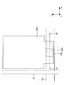
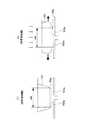
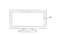
図1は、本発明の実施形態1にかかる液晶表示装置100の構成を示す断面図である。<1.
(Configuration of liquid crystal display device)
FIG. 1 is a cross-sectional view showing a configuration of a liquid
本実施形態の液晶表示装置100は、図1に示すように、液晶パネル200と、バックライト300と、データ処理部400とを有する。各部について順次説明する。 As shown in FIG. 1, the liquid
液晶パネル200は、たとえば、アクティブマトリクス方式であり、図1に示すように、TFTアレイ基板201と対向基板202と液晶層203とを有する。液晶パネル200においては、TFTアレイ基板201と対向基板202とが、互いにスペースを隔てて対向している。そして、そのTFTアレイ基板201と対向基板202との間に挟まれるように、液晶層203が設けられている。 The
液晶パネル200は、図1に示すように、TFTアレイ基板201にて対向基板202に対向する面に対して反対側の面に、第1の偏光板206が配置されている。そして、対向基板202にてTFTアレイ基板201に対向する面に対して反対側の面には、第2の偏光板207が配置されている。 As shown in FIG. 1, the
そして、液晶パネル200においては、TFTアレイ基板201の側に、バックライト300が配置されており、TFTアレイ基板201において対向基板202に対面している面に対して反対側の面に、バックライト300から出射された照明光Rが照射される。 In the
この液晶パネル200は、複数の画素(図示無し)が配置されている表示領域PAを含む。この表示領域PAにおいては、液晶パネル200の背面側に設置されたバックライト300が出射した照明光Rを、第1の偏光板206を介して背面から受け、その背面から受けた照明光Rを、その表示領域PAにおいて変調する。 The
ここでは、TFTアレイ基板201において画素に対応するように、複数のTFTが画素スイッチング素子(図示無し)として設けられており、その画素スイッチング素子が制御されることによって、背面から受けた照明光を変調する。そして、その変調された照明光Rが、第2の偏光板207を介して、正面側に出射し、表示領域PAにおいて画像が表示される。たとえば、液晶パネル200の正面の側においてカラー画像が表示される。つまり、液晶パネル200は、透過型である。 Here, a plurality of TFTs are provided as pixel switching elements (not shown) so as to correspond to the pixels in the
また、詳細については後述するが、本実施形態においては、この液晶パネル200は、抵抗膜式のタッチセンサ(図示なし)が形成されている。このタッチセンサは、液晶パネル200においてバックライト300が設置された背面に対して反対側となる正面に、ユーザーの指などの被検知体Fが接触した位置に応じて異なる電位の信号を出力するように構成されている。すなわち、液晶パネル200は、タッチパネルとして機能し、これにより、液晶表示装置100は、情報入力装置として機能する。 Although details will be described later, in the present embodiment, the
バックライト300は、図1に示すように、液晶パネル200の背面に対面しており、その液晶パネル200の表示領域PAに照明光Rを出射する。 As shown in FIG. 1, the backlight 300 faces the back surface of the
具体的には、バックライト300は、液晶パネル200においてTFTアレイ基板201の側に位置するように配置されている。そして、TFTアレイ基板201において対向基板202に対面している面に対して反対側の面に、照明光Rを照射する。つまり、バックライト300は、TFTアレイ基板201の側から対向基板202の側へ向かうように照明光Rを照明する。ここでは、バックライト300は、液晶パネル200の面の法線方向zに沿うように照明光Rを出射する。 Specifically, the backlight 300 is disposed so as to be positioned on the
データ処理部400は、図1に示すように、制御部401と、位置検出部402とを有する。データ処理部400は、コンピュータを含み、プログラムによってコンピュータが各部として動作するように構成されている。 As illustrated in FIG. 1, the
データ処理部400の制御部401は、液晶パネル200とバックライト300との動作を制御するように構成されている。制御部401は、液晶パネル200に制御信号を供給することによって、液晶パネル200に複数設けられた画素スイッチング素子(図示無し)の動作を制御する。たとえば、線順次駆動を実行させる。また、制御部401は、バックライト300に制御信号を供給することによって、バックライト300の動作を制御し、バックライト300から照明光Rを照射する。このように、制御部401は、液晶パネル200とバックライト300との動作を制御することによって、液晶パネル200の表示領域PAに画像を表示する。 The
このほかに、制御部401は、液晶パネル200に制御信号を供給することによって、液晶パネル200に設けられた抵抗膜式のタッチセンサの動作を制御し、データを収集する。 In addition, the
データ処理部400の位置検出部402は、液晶パネル200の正面側において、人体の指などの被検知体Fが接触した位置を検出するように構成されている。本実施形態においては、位置検出部402は、液晶パネル200に設けられた抵抗膜式のタッチセンサによって得たデータに基づいて、位置の検出を実施する。 The
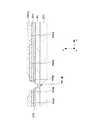
(液晶パネルの全体構成)
液晶パネル200の全体構成について説明する。(Overall configuration of LCD panel)
The overall configuration of the
図2は、本発明の実施形態1にかかる液晶パネル200を示す平面図である。 FIG. 2 is a plan view showing the
図2に示すように、液晶パネル200は、表示領域PAと、周辺領域CAとを有する。 As shown in FIG. 2, the
液晶パネル200において表示領域PAには、図2に示すように、複数の画素Pが面に沿って配置されている。 In the
具体的には、表示領域PAにおいては、複数の画素Pが水平方向xと垂直方向yとのそれぞれにマトリクス状に並ぶように配置されており、画像が表示される。詳細については後述するが、画素Pは、画素スイッチング素子(図示無し)を含む。そして、タッチセンサを構成する複数のタッチセンサスイッチ(図示無し)が、この複数の画素Pに対応するように、設けられている。 Specifically, in the display area PA, a plurality of pixels P are arranged in a matrix in each of the horizontal direction x and the vertical direction y, and an image is displayed. Although details will be described later, the pixel P includes a pixel switching element (not shown). A plurality of touch sensor switches (not shown) constituting the touch sensor are provided so as to correspond to the plurality of pixels P.
液晶パネル200において周辺領域CAは、図2に示すように、表示領域PAの周辺を囲うように位置している。この周辺領域CAにおいては、図2に示すように、垂直駆動回路11と、水平駆動回路12とが形成されている。たとえば、上記の画素スイッチング素子(図示無し)などと同様にして形成された半導体素子によって、この各回路が構成されている。 In the
そして、画素Pに対応するように設けられた画素スイッチング素子を、垂直駆動回路11および水平駆動回路12が駆動し、表示領域PAにおいて画像表示を実行する。 Then, the
また、これと共に、表示領域PAに設けられたタッチセンサ(図示なし)を、垂直駆動回路11および水平駆動回路12が駆動し、データの取得を実行する。そして、液晶パネル200の表示領域PAにユーザーの指などの被検知体が接触した位置を、そのタッチセンサによって取得したデータに基づいて、位置検出部402が検出する。 At the same time, the
(液晶パネルの詳細構成)
液晶パネル200の詳細な構成について説明する。(Detailed configuration of LCD panel)
A detailed configuration of the
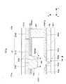
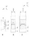
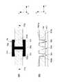
図3から図5は、本発明の実施形態1にかかる液晶パネル200の要部を示す図である。 3 to 5 are views showing the main part of the
ここで、図3は、本発明の実施形態1にかかる液晶パネル200において、表示領域PAに設けられた画素Pの概略を模式的に示す断面図である。 Here, FIG. 3 is a cross-sectional view schematically showing an outline of the pixel P provided in the display area PA in the
また、図4は、本発明にかかる実施形態1において、液晶パネル200の表示領域PAに設けられた画素Pの概略を模式的に示す上面図である。図4は、画素Pを構成する複数のサブ画素の一部を示しており、図3は、図4のX1−X2部分に相当する。図示の都合上、適宜、省略やスケールの変更等をして、各部材を示している。 FIG. 4 is a top view schematically showing an outline of the pixel P provided in the display area PA of the
そして、図5は、本発明の実施形態1にかかる液晶パネル200の概略を示す回路図である。 FIG. 5 is a circuit diagram schematically showing the
液晶パネル200は、図3に示すように、TFTアレイ基板201と対向基板202との間には、柱スペーサSPが介在しており、シール材(図示無し)で貼り合わされている。そして、そのTFTアレイ基板201と対向基板202との間には、液晶層203が封入されている。 As shown in FIG. 3, the
本実施形態においては、図3に示すように、液晶パネル200は、タッチセンサスイッチSWsが内蔵されている。このタッチセンサスイッチSWsは、図3に示すように、一対のタッチ電極62t,25によって構成されている。 In the present embodiment, as shown in FIG. 3, the
液晶パネル200において、TFTアレイ基板201は、光を透過する絶縁体の基板であり、たとえば、ガラスにより形成されている。このTFTアレイ基板201においては、図3に示すように、対向基板202に対向する側の面に、画素電極62pと、タッチセンサスイッチSWsを構成する一方のタッチ電極62tと、ゲート線GLと、液晶配向膜HM1とが形成されている。 In the
液晶パネル200において、対向基板202は、TFTアレイ基板201と同様に、光を透過する絶縁体の基板であり、たとえば、ガラスにより形成されている。この対向基板202においては、図3に示すように、TFTアレイ基板201に対向する側の面に、カラーフィルタ層21と、共通電極23と、タッチ電極25と、液晶配向膜HM2とが形成されている。ここでは、カラーフィルタ層21は、図3に示すように、赤フィルタ層21Rと、緑フィルタ層21Gと、青フィルタ層21Bとを一組として構成されている。 In the
液晶パネル200は、図3に示した部材のほかに、図4に示すように、信号線SLを含む。また、図5に示すように、画素スイッチング素子31を含む。信号線SLと画素スイッチング素子31とのそれぞれは、図3では図示されていないが、液晶パネル200を構成するTFTアレイ基板201に設けられている。 The
TFTアレイ基板201に設けられた各部について示す。 Each part provided on the
TFTアレイ基板201において、画素電極62pとタッチ電極62tとのそれぞれは、図3に示すように、TFTアレイ基板201にて対向基板202に対面する面上に設けられている。ここでは、画素電極62pとタッチ電極62tとのそれぞれは、層間絶縁膜Sz1を介して設けられている。画素電極62pとタッチ電極62tのそれぞれは、いわゆる透明電極であって、たとえば、ITOを用いて形成されている。 In the
タッチ電極62tは、図3に示すように、ゲート線GLの上方に設けられている。たとえば、タッチ電極62tは、カラーフィルタ層21を構成する赤フィルタ層21Rに対応するように、設けられている。つまり、画素Pを構成する3つのサブ画素のうち、1つのサブ画素に対応するように、タッチ電極62tが形成されている。そして、タッチ電極62tは、液晶層203を介して、対向基板202に設けられた1つのタッチ電極25に対面している。 The
また、図4に示すように、タッチ電極62tは、画素電極62pと一体になるように形成されている。すなわち、タッチ電極62tは、画素電極62pと電気的に接続している。 As shown in FIG. 4, the
そして、図5に示すように、タッチ電極62tは、画素スイッチング素子31に電気的に接続されている。 As shown in FIG. 5, the
本実施形態においては、タッチ電極62tは、図3に示すように、弾性部材63の頂面を被覆するように設けられている。 In the present embodiment, the
図3に示すように、弾性部材63は、ゲート線GLの上方において、層間絶縁膜Sz1を介在して設けられている。弾性部材63は、この層間絶縁膜Sz1上において、対向基板202へ向かう方向へ、凸状に突出するように設けられている。たとえば、弾性部材63は、感光性のアクリル樹脂膜をパターン加工することで形成されている。ここでは、図3に示すように、弾性部材63は、タッチ電極62tが被覆された状態において、セルギャップを保持する柱スペーサSPよりも、高さが低くなるように形成されている。 As shown in FIG. 3, the
画素電極62pは、図4に示すように、xy面において、ゲート線GLと信号線SLとによって区画される複数の領域のそれぞれに対応するように、矩形パターンで形成されている。カラーフィルタ層21を構成する赤フィルタ層21R以外の緑フィルタ層21Gと青フィルタ層21Bとのそれぞれにおいても、これと同様な平面形状になるように形成されている。つまり、画素Pを構成する3つのサブ画素のそれぞれに対応するように、画素電極62pが形成されている。 As shown in FIG. 4, the
ここでは、画素電極62pは、図3に示すように、液晶層203を介して、共通電極23に対面している。また、図5に示すように、画素電極62pは、画素スイッチング素子31に電気的に接続されており、画素スイッチング素子31がオン状態の際に、液晶層203に電位を与えるように構成されている。 Here, the
TFTアレイ基板201において、画素スイッチング素子31は、図3では図示を省略しているが、TFTアレイ基板201にて対向基板202に対向する側の面上において、層間絶縁膜Sz1内に設けられている。 In the
ここで、画素スイッチング素子31は、図5に示すように、トランジスタであって、たとえば、ポリシリコンを用いたTFTとして構成されている。この画素スイッチング素子31は、図5に示すように、ゲートが、ゲート線GLに電気的に接続されている。そして、ドレインが、信号線SLに電気的に接続されている。そして、ソースが、画素電極62pと、タッチ電極62tとのそれぞれに接続されている。 Here, as shown in FIG. 5, the
TFTアレイ基板201において、ゲート線GLは、図3に示すように、TFTアレイ基板201にて対向基板202に対向する側の面上に設けられている。 In the
そして、図4,図5に示すように、ゲート線GLは、xy面において、x方向に延在するように設けられている。たとえば、ゲート線GLは、モリブデンなどの金属材料を用いて形成されている。そして、ゲート線GLは、図5に示すように、画素スイッチング素子31のゲートに電気的に接続されている。この他に、ゲート線GLは、図5に示すように、垂直駆動回路11に電気的に接続されており、垂直駆動回路11から走査信号Vgateを画素スイッチング素子31のゲートに供給する。 4 and 5, the gate line GL is provided to extend in the x direction on the xy plane. For example, the gate line GL is formed using a metal material such as molybdenum. The gate line GL is electrically connected to the gate of the
TFTアレイ基板201において、信号線SLは、図3では図示を省略しているが、TFTアレイ基板201にて対向基板202に対向する側の面上において、層間絶縁膜Sz1内に設けられている。 In the
そして、図4,図5に示すように、信号線SLは、xy面において、y方向に延在するように設けられている。そして、信号線SLは、図5に示すように、画素スイッチング素子31のドレインに電気的に接続されている。この他に、信号線SLは、図5に示すように、水平駆動回路12に電気的に接続するように構成されている。 4 and 5, the signal line SL is provided to extend in the y direction on the xy plane. The signal line SL is electrically connected to the drain of the
本実施形態では、水平駆動回路12は、図5に示すように、書き込み回路WCと、読み出し回路RCとを含む。信号線SLは、書き込み回路WCとの間に、スイッチSWwが介在しており、スイッチSWwがオン状態になったときに、書き込み回路WCに電気的に接続するように構成されている。また、信号線SLは、読み出し回路RCとの間に、スイッチSWrが介在しており、スイッチSWrがオン状態になったときに、読み出し回路RCに電気的に接続するように構成されている。詳細については後述するが、この2つのスイッチSWw,SWrは、差動的に動作し、同時にオン状態にならないように、動作が制御される。このため、スイッチSWwがオン状態にされたときには、信号線SLは、書き込み回路WCに電気的に接続し、書き込み回路WCからライト信号(WRIRHT)が供給される。そして、スイッチSWrがオン状態になったときには、信号線SLは、読み出し回路RCに電気的に接続し、読み出し回路RCからリード信号(READ)が供給される。 In the present embodiment, the
TFTアレイ基板201において液晶配向膜HM1は、図3に示すように、TFTアレイ基板201にて対向基板202に対面する面上にて、画素電極62pおよびタッチ電極62tを介して設けられている。たとえば、この液晶配向膜HM1は、ポリイミドによって形成されている。 In the
本実施形態においては、この液晶配向膜HM1は、タッチ電極62tの表面が露出するように形成されている。 In the present embodiment, the liquid crystal alignment film HM1 is formed so that the surface of the
対向基板202に設けられた各部について示す。 Each part provided on the
対向基板202において、カラーフィルタ層21は、図3に示すように、対向基板202にてTFTアレイ基板201に対向する側の面に形成されている。ここでは、カラーフィルタ層21は、赤フィルタ層21Rと緑フィルタ層21Gと青フィルタ層21Bとの3原色のフィルタを1組として画素Pごとに設けられており、それぞれの色が、x方向に並ぶように形成されている。カラーフィルタ層21は、たとえば、顔料や染料などの着色剤を含有するポリイミド樹脂を用いて形成されている。このカラーフィルタ層21においては、バックライト300から照射された白色光が着色されて出射される。 In the
対向基板202において、共通電極23は、図3に示すように、対向基板202にてTFTアレイ基板201に対面する側の面に形成されている。ここで、共通電極23は、カラーフィルタ層21上に形成された層間絶縁膜Sz2を被覆するように形成されている。共通電極23は、いわゆる透明電極であって、たとえば、ITOを用いて形成されている。 In the
そして、図5に示すように、共通電極23は、Vcom線CLに電気的に接続されており、共通電位が印加される。つまり、共通電極23は、表示領域PAにおいて、複数の画素Pに対応するように形成された複数の画素電極62pのそれぞれに対向しており、各画素Pにおいて共通な電極として機能するように構成されている。 As shown in FIG. 5, the
対向基板202において、タッチ電極25は、図3に示すように、対向基板202にてTFTアレイ基板201に対面する側の面に形成されている。ここでは、図3に示すように、タッチ電極25は、共通電極23と同様に、層間絶縁膜Sz2を被覆しており、共通電極23と一体であって同層になるように形成されている。つまり、タッチ電極25は、共通電極23と同様に、いわゆる透明電極であって、たとえば、ITOを用いて形成されている。そして、タッチ電極25は、図3に示すように、液晶パネル200が外圧によって変形した際には、対向するタッチ電極62tに接触して電気的に接続するように構成されている。 In the
また、図5に示すように、タッチ電極25は、共通電極23と同様に、Vcom線CLに電気的に接続されており、共通電位が印加される。 Further, as shown in FIG. 5, the
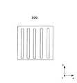
本実施形態においては、タッチ電極25は、図3に示すように、凹凸領域500の表面を被覆するように設けられている。 In the present embodiment, the
凹凸領域500は、図3に示すように、対向基板202にてTFTアレイ基板201に対向する面であって、層間絶縁膜Sz2の表面に形成されている。凹凸領域500は、図3に示すように、TFTアレイ基板201に設けられた弾性部材63の幅W1よりも、幅W2が広くなるように設けられている。そして、凹凸領域500は、TFTアレイ基板201において弾性部材63上に設けられたタッチ電極62tとの間において、所定のセンサギャップΔdが介在している。 As shown in FIG. 3, the
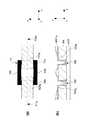
図6と図7は、本発明にかかる実施形態1において、凹凸領域500の部分を拡大して示す図である。 FIGS. 6 and 7 are enlarged views of the
図6は、凹凸領域500の部分を拡大して示す断面図である。一方、図7は、凹凸領域500の部分を拡大して示す上面図である。 FIG. 6 is an enlarged cross-sectional view showing a portion of the
図6,図7に示すように、凹凸領域500においては、層間絶縁膜Sz2の表面に、複数の溝が間を隔てて形成されている。 As shown in FIGS. 6 and 7, in the
ここでは、図7に示すように、たとえば、複数の溝が、y方向に延在しており、この複数の溝が、x方向に間を空けて並んでいる。 Here, as shown in FIG. 7, for example, a plurality of grooves extend in the y direction, and the plurality of grooves are arranged with an interval in the x direction.
対向基板202において、液晶配向膜HM2は、図3に示すように、共通電極23上に設けられている。ここでは、液晶配向膜HM2は、共通電極23の表面全面を被覆するように、設けられている。この液晶配向膜HM2は、共通電極23およびタッチ電極25が形成された表面上に配向材料を塗布することによって形成される。たとえば、液晶配向膜HM2は、ポリイミドを用いて形成される。 In the
詳細については後述するが、凹凸領域500は、凸部と凹部とが交互に設けられているので、凸部の頂面に配向材料が成膜されないため、液晶配向膜HM2は、この頂面に形成されずに、その表面が露出するように形成されている。 Although details will be described later, since the convex and
液晶層203について示す。 The
液晶層203は、図3に示すように、TFTアレイ基板201と対向基板202との間にて挟持されている。 As shown in FIG. 3, the
ここでは、液晶層203は、TFTアレイ基板201に形成された液晶配向膜HM1と、対向基板202に形成された液晶配向膜HM2とによって、液晶分子(図示なし)が配向されている。たとえば、液晶分子が垂直配向するように液晶層203が形成されている。つまり、液晶表示モードが、VA(Vertical Align)モードになるように、液晶層203が形成されている。 Here, in the
この他に、TN(Twisted Nematic)モード、ECB(Electrically Controlled Birefringence)モードに対応するように、液晶層203を形成しても良い。 In addition, the
(動作)
以下より、上記の液晶表示装置100において、ユーザーの指などの被検知体Fが液晶パネル200の表示領域PAに接触した位置を検出する際の動作について説明する。(Operation)
Hereinafter, in the liquid
図8は、本発明の実施形態1にかかる液晶表示装置100を動作させる際に、制御部401が、各部に供給する制御信号の波形図である。 FIG. 8 is a waveform diagram of control signals supplied from the
図8において、(A)は、ゲート線GLに供給する走査信号(Vgate)を示している。(B)は、信号線SLに供給するデータ信号(Vsig)を示している。(C)は、Vcom線CLに供給する共通電圧(Vcom)の波形図である。(D)は、スイッチSWwに供給するライト信号(Write)を示している。(E)は、スイッチSWrに供給するリード信号(Read)を示している。 8A shows a scanning signal (Vgate) supplied to the gate line GL. (B) shows a data signal (Vsig) supplied to the signal line SL. (C) is a waveform diagram of the common voltage (Vcom) supplied to the Vcom line CL. (D) shows a write signal (Write) supplied to the switch SWw. (E) shows a read signal (Read) supplied to the switch SWr.
まず、T1においては、図8の(B)と(D)とに示すように、データ信号(Vsig)とライト信号(Write)とが、ローレベルからハイレベルになる。このため、ハイレベルのライト信号(Write)によって、スイッチSWwがオンになり、ハイレベルのデータ信号(Vsig)が、スイッチSWwを介して、書き込み回路WCから信号線SLへ供給される(図5参照)。 First, at T1, as shown in FIGS. 8B and 8D, the data signal (Vsig) and the write signal (Write) change from the low level to the high level. Therefore, the switch SWw is turned on by the high level write signal (Write), and the high level data signal (Vsig) is supplied from the write circuit WC to the signal line SL via the switch SWw (FIG. 5). reference).
つぎに、T2においては、図8の(D)に示すように、ライト信号(Write)がローレベルになって、スイッチSWwがオフになり、信号線SLが、フローティング状態になる。この状態で、T2においては、図8の(A)に示すように、走査信号(Vgate)が、ローレベルからハイレベルになる。このため、画素スイッチング素子31のゲートがオン状態になり、画素スイッチング素子31においては、チャネルが形成されて、データ信号(Vsig)の電荷の放電経路が生ずる(図5参照)。 Next, at T2, as shown in FIG. 8D, the write signal (Write) becomes low level, the switch SWw is turned off, and the signal line SL enters a floating state. In this state, at T2, as shown in FIG. 8A, the scanning signal (Vgate) changes from the low level to the high level. Therefore, the gate of the
このとき、タッチセンサスイッチSWsがオン状態にされた場合には、大きな容量のVcom線CLに、フローティング状態の信号線SLの電荷が放電される。このため、図8の(B)にて実線で示すように、データ信号(Vsig)の電位が、大きく低下する。 At this time, when the touch sensor switch SWs is turned on, the charge of the floating signal line SL is discharged to the large-capacity Vcom line CL. For this reason, as indicated by a solid line in FIG. 8B, the potential of the data signal (Vsig) greatly decreases.
一方で、タッチセンサスイッチSWsがオフ状態である場合には、図8の(B)にて破線で示すように、データ信号(Vsig)の電位は、ほぼ保持されて、変化が少ない。 On the other hand, when the touch sensor switch SWs is in the OFF state, as shown by a broken line in FIG. 8B, the potential of the data signal (Vsig) is substantially held and changes little.
つぎに、T3においては、図8の(E)に示すように、リード信号(Read)が、ローレベルからハイレベルになる。このため、ハイレベルのリード信号(Read)によって、スイッチSWrがオンになり、データ信号(Vsig)が、スイッチSWrを介して、信号線SLから読み出し回路RCへ読み出される(図5参照)。 Next, at T3, as shown in FIG. 8E, the read signal (Read) changes from the low level to the high level. Therefore, the switch SWr is turned on by the high level read signal (Read), and the data signal (Vsig) is read from the signal line SL to the read circuit RC via the switch SWr (see FIG. 5).
ここで、タッチセンサスイッチSWsがオン状態である場合には、図8の(B)にて実線で示したように、低い電位のデータ信号(Vsig)が読み出される。一方で、タッチセンサスイッチSWsがオフ状態である場合には、図8の(B)にて破線で示したように、高い電位のデータ信号(Vsig)が読み出される。 Here, when the touch sensor switch SWs is in an ON state, a low potential data signal (Vsig) is read as shown by a solid line in FIG. On the other hand, when the touch sensor switch SWs is in an off state, a high potential data signal (Vsig) is read as indicated by a broken line in FIG.
そして、このとき、この読み出したデータ信号(Vsig)の電位に基づいて、データ処理部400の位置検出部402(図1参照)が、位置検出を行う。 At this time, based on the read potential of the data signal (Vsig), the position detection unit 402 (see FIG. 1) of the
具体的には、位置検出部402は、読み出したデータ信号(Vsig)の電位と参照電位との比較処理を実行し、参照電位よりも大きい場合には、タッチセンサスイッチSWsがオフ状態であると判断する。一方で、読み出したデータ信号(Vsig)の電位が、参照電位に対して小さい場合には、タッチセンサスイッチSWsがオン状態であると判断する。そして、位置検出部402は、タッチセンサスイッチSWsがオン状態であると判断した画素Pの位置を、指などの被検知体Fが接触した位置として検出する。 Specifically, the
つまり、位置検出部402は、タッチセンサスイッチSWsがオン状態の場合と、オフ状態の場合との間において、変化する電位に基づいて、液晶パネル200にて、指などの被検知体Fが接触した位置を検出する。 That is, the
つぎに、T4においては、図8の(E)に示すように、リード信号(Read)を、ローレベルにし、スイッチSWrをオフ状態にする。そして、ライト信号(Write)を、ローレベルからハイレベルとして、スイッチSWwをオン状態にすると共に、信号線SLにハイレベルのデータ信号(Vsig)を印加する。その後、共通電圧Vcomの電位を反転して、表示の制御を続行する。 Next, at T4, as shown in FIG. 8E, the read signal (Read) is set to low level, and the switch SWr is turned off. Then, the write signal (Write) is changed from the low level to the high level, the switch SWw is turned on, and the high-level data signal (Vsig) is applied to the signal line SL. Thereafter, the potential of the common voltage Vcom is inverted, and display control is continued.
(製造方法)
以下より、上記の液晶表示装置100の要部である凹凸領域500の部分を形成する方法について説明する。(Production method)
Hereinafter, a method of forming a portion of the
図9は、本発明の実施形態1にかかる液晶表示装置100において、凹凸領域500の部分を形成する工程を示す断面図である。図9では、要部を示しており、一部の部材については、表示を省略している。 FIG. 9 is a cross-sectional view illustrating a process of forming the
まず、図9(a)に示すように、層間絶縁膜Sz2を形成する。 First, as shown in FIG. 9A, an interlayer insulating film Sz2 is formed.
ここでは、たとえば、感光性樹脂(図示なし)を塗布することによって、この層間絶縁膜Sz2を形成する。たとえば、ポジ型の感光性であるアクリル樹脂を塗布後、プリベーク処理を実施することで、層間絶縁膜Sz2を形成する。 Here, for example, this interlayer insulating film Sz2 is formed by applying a photosensitive resin (not shown). For example, after applying a positive photosensitive acrylic resin, a pre-bake treatment is performed to form the interlayer insulating film Sz2.
つぎに、図9(b)に示すように、層間絶縁膜Sz2に溝を形成する。 Next, as shown in FIG. 9B, a groove is formed in the interlayer insulating film Sz2.
ここでは、フォトリソグラフィ技術によって、感光性樹脂からなる層間絶縁膜Sz2をパターン加工することで、溝を形成し、凹凸領域500を設ける。 Here, the interlayer insulating film Sz2 made of a photosensitive resin is patterned by a photolithography technique to form a groove and provide the
具体的には、マスクパターンが形成されたフォトマスクを用いて露光処理を実施する。この露光処理では、溝を形成する部分へ、露光光を照射する。ここでは、露光量を適宜調整して、露光光の照射を実施する。 Specifically, an exposure process is performed using a photomask on which a mask pattern is formed. In this exposure process, exposure light is irradiated to a portion where a groove is to be formed. Here, exposure is performed by appropriately adjusting the exposure amount.
そして、この露光処理の実施後に、現像処理を実施する。この後、ベーク処理の実施によって、層間絶縁膜Sz2中の残留溶剤や低分子の未重合成分を揮発させる。このようにすることで、図9(b)に示すように、層間絶縁膜Sz2の表面に溝が形成される。 Then, after this exposure processing, development processing is performed. Thereafter, the residual solvent and low-molecular unpolymerized components in the interlayer insulating film Sz2 are volatilized by performing a baking process. By doing so, as shown in FIG. 9B, a groove is formed on the surface of the interlayer insulating film Sz2.
なお、上記の露光処理においては、一のフォトマスクを用いて形成する場合のみならず、適宜、複数のフォトマスクを組み合わせて、露光処理を実施しても良い。また、上記の溝の他に、図示をしていないが、コンタクトホールを、別途、同一工程で形成しても良い。 In the above-described exposure process, the exposure process may be performed by appropriately combining a plurality of photomasks as well as the case of forming using one photomask. In addition to the groove, although not shown, the contact hole may be separately formed in the same process.
つぎに、図9(c)に示すように、タッチ電極25を形成する。 Next, as shown in FIG. 9C, the
ここでは、層間絶縁膜Sz2にて溝が形成された表面に、透明な導電材料を成膜することで、タッチ電極25を形成する。たとえば、スパッタリング法によって、ITOを成膜することで、タッチ電極25を形成する。 Here, the
この他に、図9(c)に示すように、共通電極23についても、これと同一工程で形成する。 In addition, as shown in FIG. 9C, the
つぎに、図9(d)に示すように、液晶配向膜HM2を形成する。 Next, as shown in FIG. 9D, a liquid crystal alignment film HM2 is formed.
ここでは、タッチ電極25および共通電極23上に配向材料を塗布し成膜することによって、液晶配向膜HM2を形成する。たとえば、スピンコート法によって、配向材料が溶解された塗布液を塗布する。そして、プリベーク処理によって、塗布膜中の溶媒を揮発させた後、本ベーク処理で残留溶剤を除去する。これにより、たとえば、ポリイミドの液晶配向膜HM2を形成する。スピンコート法の他に、オフセット印刷などによって、液晶配向膜HM2を形成しても良い。 Here, the liquid crystal alignment film HM2 is formed by applying and forming an alignment material on the
図9(d)に示すように、凹凸領域500の表面においては、凸部と凹部とが交互に設けられているので、凸部の頂面には、配向材料が成膜されない。具体的には、配向材料が溶解された塗布液が、凹凸領域500の凹部の内部に入り、凸部の頂面を被覆しない。このため、この凹凸領域500において凸部の頂面の表面には、液晶配向膜HM2が成膜されず、タッチ電極25の表面が露出するように形成される。 As shown in FIG. 9D, since the convex portions and the concave portions are alternately provided on the surface of the concave and
この後、配向処理を実施する。たとえば、ラビング処理によって配向処理を実施する。この他に、光配向処理、イオンビーム配向処理、グレーティング配向処理などの配向処理を実施しても良い。なお、たとえば、液晶配向膜HM2が、垂直配向を誘起するものである場合であって、液晶パネル200を垂直配向モードにする場合には、配向処理を別途実施する必要はない。 Thereafter, alignment treatment is performed. For example, the alignment process is performed by a rubbing process. In addition, an alignment process such as a photo alignment process, an ion beam alignment process, or a grating alignment process may be performed. For example, when the liquid crystal alignment film HM2 induces vertical alignment and the
そして、図3に示したように、各部が形成された対向基板202と、TFTアレイ基板201とを貼り合わせる。その後、TFTアレイ基板201と対向基板202との間に、液晶材料を注入して液晶層203を設けることによって、液晶パネル200を完成させる。 Then, as shown in FIG. 3, the
(まとめ)
以上のように、本実施形態において、タッチセンサスイッチSWsを構成するタッチ電極25は、複数の溝が間を隔てて形成された凹凸領域500の表面を被覆するように設けられている。そして、液晶配向膜HM2は、タッチ電極25が形成された表面上に配向材料を塗布することによって形成されており、タッチ電極25において凹凸領域500の凸部の頂面の表面が露出している。このように、本実施形態では、タッチ電極25を凹凸領域500の表面に沿って形成していることから、この部分の液晶配向膜HM2を除去する工程を別途実施せずに、凸部の頂面の表面を露出させることができる。(Summary)
As described above, in the present embodiment, the
よって、本実施形態は、製造効率,歩留まりの向上を実現することができる。また、インクジェットの設備などのように、新規な設備を導入することが必要でないので、製造コストが増加することを防止できる。そして、本実施形態においては、対向基板202に設けられたタッチ電極25と、TFTアレイ基板201に設けられたタッチ電極62tとを、接触時に好適に導通させることができるので、装置の信頼性を向上させることができる。 Therefore, this embodiment can realize improvement in manufacturing efficiency and yield. Further, since it is not necessary to introduce new equipment such as an ink jet equipment, an increase in manufacturing cost can be prevented. In this embodiment, since the
また、本実施形態においては、凹凸領域500を、タッチ電極25が被覆された状態において、凸部の幅Lが、0.5から5.0μmであって、凹部の幅Sが、0.5から5.0μmになるように形成することが好適である。また、さらに、凸部の頂面と凹部の底面との距離(高さ)Hが、0.5〜2.0μmになるように形成することが好適である。このようにすることで、タッチ電極25において凹凸領域500の凸部の頂面の表面が液晶配向膜HM2で被覆されずに露出させることを、好適に、実現できる。 In this embodiment, in the state where the
図10と図11は、本発明の実施形態1にかかる液晶表示装置100において、凸部の幅L(μm)および高さH(μm)と、液晶配向膜の被覆率(%)との関係を示す図である。 10 and 11 show the relationship between the width L (μm) and the height H (μm) of the protrusion and the coverage (%) of the liquid crystal alignment film in the liquid
図10は、横軸が、高さH(μm)であって、縦軸が、液晶配向膜の被覆率(%/100)である。そして,(a),(b),(c)のそれぞれにおいて、凸部の幅L(μm)が、0.3μm,0.8μm,1.2μmである場合の結果を示している。なお、凹部の幅Sについても、この凸部の幅Lと同じになるように形成している。 In FIG. 10, the horizontal axis represents the height H (μm), and the vertical axis represents the coverage (% / 100) of the liquid crystal alignment film. In each of (a), (b), and (c), the results are shown when the width L (μm) of the convex portions is 0.3 μm, 0.8 μm, and 1.2 μm. Note that the width S of the concave portion is also formed to be the same as the width L of the convex portion.
一方で、図11は、図10において示した2つの被覆率R1,R2を示す図である。図11に示すように、被覆率R1は、下記の数式(1)で示され、被覆率R2は、下記の数式(2)で示される。ここで、Pは、図11(a),(b)に示すように、複数の凹部の間におけるピッチPである。そして、P1は、図11(a)に示すように、凸部において、液晶配向膜HM2が被覆されない幅である。また、P2は、図11(b)に示すように、凸部において、凹部の底面に設けられた液晶配向膜HM2の半分の膜厚になる部分の幅である。 On the other hand, FIG. 11 is a diagram showing the two coverages R1 and R2 shown in FIG. As shown in FIG. 11, the coverage ratio R1 is represented by the following mathematical formula (1), and the coverage ratio R2 is represented by the following mathematical formula (2). Here, P is the pitch P between the plurality of recesses, as shown in FIGS. And P1 is a width | variety which liquid crystal aligning film HM2 is not coat | covered in a convex part, as shown to Fig.11 (a). Further, P2 is the width of the portion of the convex portion that is half the thickness of the liquid crystal alignment film HM2 provided on the bottom surface of the concave portion, as shown in FIG.
R1=(P−P1)/P ・・・(1)
R2=(P−P2)/P ・・・(2)R1 = (P−P1) / P (1)
R2 = (P−P2) / P (2)
図10の結果から判るように、凸部の幅Lが、0.5μm以上であって、その高さHが、0.5μm以上にすることで、液晶配向膜HM2が、全面に被覆されない。 As can be seen from the result of FIG. 10, the liquid crystal alignment film HM2 is not covered on the entire surface when the width L of the convex portion is 0.5 μm or more and the height H is 0.5 μm or more.
そして、上述した上限値を超える場合には、凸部上に配向膜が残ってしまう等の不具合が生ずる場合がある。このような結果は、塗布液の液粘度が、30mPa・sが中心値であって、1〜500mPa・sの範囲において得ることができる。 And when exceeding the upper limit mentioned above, malfunctions, such as an alignment film remaining on a convex part, may arise. Such a result can be obtained in the range of 1 to 500 mPa · s, with the liquid viscosity of the coating solution being 30 mPa · s as the central value.
よって、上記した数値範囲において、凹凸領域500を形成することが好適である。 Therefore, it is preferable to form the
なお、上記においては、凹凸領域500が、図7に示したように形成されている場合について説明したが、これに限定されない。 In the above description, the case where the
図12と図13は、本発明にかかる実施形態1の変形例において、凹凸領域500の部分を拡大して示す図である。図12と図13は、上面図である。 FIGS. 12 and 13 are enlarged views of the
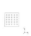
図12に示すように、凹凸領域500においては、複数の溝をx方向とy方向とにマトリクス状に並ぶように形成してもよい。 As shown in FIG. 12, in the
また、図13に示すように、凹凸領域500においては、複数の溝を円形に形成してもよい。 Moreover, as shown in FIG. 13, in the uneven | corrugated area |
この他に、上記においては、層間絶縁膜Sz2の表面をフォトリソグラフィ技術によって加工し、その表面に溝を形成することで、凹凸領域500を設ける場合について説明したが、これに限定されない。 In addition to the above, the case where the
図14は、本発明にかかる実施形態1の変形例において、液晶パネル200の要部を示す図である。ここで、図14は、表示領域PAに設けられた画素Pの概略を模式的に示す断面図である。 FIG. 14 is a diagram showing a main part of the
図14に示すように、カラーフィルタ層21において赤カラーフィルタ層21Raの表面を、フォトリソグラフィ技術によって加工し、その表面に溝を形成することで、凹凸領域500を設けてもよい。 As shown in FIG. 14, the surface of the red color filter layer 21Ra in the
<2.実施形態2>
以下より、本発明にかかる実施形態2について説明する。<2. Second Embodiment>
Hereinafter,
(液晶パネルの詳細構成)
図15は、本発明の実施形態2にかかる液晶パネル200bの要部を示す図である。ここで、図15は、本発明の実施形態2にかかる液晶パネル200bにおいて、表示領域PAに設けられた画素Pの概略を模式的に示す断面図である。(Detailed configuration of LCD panel)
FIG. 15 is a diagram illustrating a main part of the
図15に示すように、本実施形態においては、タッチセンサスイッチSWsbの構成が、実施形態1と異なる。具体的には、図15と図3とを比較してわかるように、対向基板202に形成されたタッチ電極25bが、実施形態1と異なる。また、TFTアレイ基板201に形成されたタッチ電極62tbが、実施形態1と異なる。この点、および、これに関連する点を除き、実施形態1と同様である。このため、重複する箇所については、説明を省略する。 As shown in FIG. 15, in the present embodiment, the configuration of the touch sensor switch SWsb is different from that of the first embodiment. Specifically, as can be seen by comparing FIG. 15 and FIG. 3, the
対向基板202において、タッチ電極25bは、図15に示すように、弾性部材63bの頂面を被覆するように設けられている。 In the
図15に示すように、弾性部材63bは、層間絶縁膜Sz2上に設けられている。弾性部材63bは、この層間絶縁膜Sz2上において、TFTアレイ基板201へ向かう方向へ、凸状に突出するように設けられている。たとえば、弾性部材63bは、感光性のアクリル樹脂膜をパターン加工することで形成されている。ここでは、図15に示すように、弾性部材63bは、柱スペーサSPよりも、高さが低くなるように形成されている。 As shown in FIG. 15, the
そして、図15に示すように、対向基板202において、弾性部材63bが設けられた領域以外の表面を被覆するように、液晶配向膜HM2bが設けられている。ここでは、液晶配向膜HM2bは、共通電極23およびタッチ電極25bが形成された表面上に配向材料を塗布することによって形成される。弾性部材63bは、対向基板202の表面にて凸状に突き出ているので、その頂面に位置する部分においては、配向材料が塗布されず、タッチ電極25bの表面が露出している。 As shown in FIG. 15, the
TFTアレイ基板201において、タッチ電極62tbは、図15に示すように、凹凸領域500bの表面を被覆するように設けられている。 In the
凹凸領域500bは、図15に示すように、TFTアレイ基板201にて対向基板202に対向する面であって、層間絶縁膜Sz1の表面に形成されている。凹凸領域500bは、図15に示すように、対向基板202に設けられた弾性部材63bの幅W1bよりも、その幅W2bが広くなるように設けられている。そして、凹凸領域500bは、対向基板202において弾性部材63b上に設けられたタッチ電極25bとの間において、所定のセンサギャップΔdbが介在している。 As shown in FIG. 15, the
この凹凸領域500bは、実施形態1の場合と同様に、複数の溝が設けられており、その表面に沿って、タッチ電極62tbが形成されている。つまり、凹凸領域500bの表面においては、凸部と凹部とが交互に設けられている。 As in the case of the first embodiment, the
そして、図15に示すように、凹凸領域500b上においては、液晶配向膜HM1bが設けられている。ここでは、液晶配向膜HM1bは、画素電極62pおよびタッチ電極62tが形成された表面上に配向材料を塗布することによって形成される。凹凸領域500bの表面においては、凸部と凹部とが交互に設けられているので、実施形態1の場合と同様に、配向材料が成膜されない。このため、凹凸領域500bの凸部の頂面に位置する部分においては、タッチ電極62tbの表面が露出している。 And as shown in FIG. 15, liquid crystal aligning film HM1b is provided on the uneven | corrugated area |
(まとめ)
以上のように、本実施形態において、タッチセンサスイッチSWsbを構成するタッチ電極62tbは、複数の溝が間を隔てて形成された凹凸領域500bの表面を被覆するように設けられている。そして、液晶配向膜HM1bは、タッチ電極62tbが形成された表面上に配向材料を塗布することによって形成されており、タッチ電極62tbにおいて凹凸領域500bの凸部の頂面の表面が露出している。(Summary)
As described above, in the present embodiment, the touch electrode 62tb constituting the touch sensor switch SWsb is provided so as to cover the surface of the
本実施形態では、タッチ電極62tbを凹凸領域500bの表面に沿って形成することで、凹凸領域500bにおいて凸部の頂面に位置するタッチ電極62tbの表面を露出させることができる。つまり、本実施形態は、この部分の液晶配向膜HM1bを除去する工程を別途実施する必要がない。 In the present embodiment, by forming the touch electrode 62tb along the surface of the concavo-
よって、本実施形態は、実施形態1の場合と同様に、製造効率,歩留まりの向上が可能であって、製造コストが増加することを防止できる。また、装置の信頼性を向上させることができる。 Therefore, as in the case of the first embodiment, this embodiment can improve manufacturing efficiency and yield, and can prevent an increase in manufacturing cost. In addition, the reliability of the apparatus can be improved.
なお、上記においては、層間絶縁膜Sz1の表面をフォトリソグラフィ技術によって加工し、その表面に溝を形成することで、凹凸領域500bを設ける場合について説明したが、これに限定されない。 In the above description, the surface of the interlayer insulating film Sz1 is processed by a photolithography technique and a groove is formed on the surface to provide the
図16は、本発明にかかる実施形態2の変形例において、液晶パネル200bの要部を示す図である。ここで、図16は、表示領域PAに設けられた画素Pの概略を模式的に示す断面図である。 FIG. 16 is a diagram illustrating a main part of the
図16に示すように、TFTアレイ基板201の表面に、凸状に突出する下地層OPを、複数設ける。そして、この複数の下地層OPを被覆するように、層間絶縁膜Sz1を形成することで、凹凸領域500bを設けてもよい。 As shown in FIG. 16, a plurality of base layers OP protruding in a convex shape are provided on the surface of the
<3.実施形態3>
以下より、本発明にかかる実施形態3について説明する。<3. Embodiment 3>
Hereinafter, Embodiment 3 according to the present invention will be described.
(液晶パネルの詳細構成)
図17は、本発明の実施形態3にかかる液晶パネル200cの要部を示す図である。ここで、図17は、本実施形態の液晶パネル200cにおいて、表示領域PAに設けられた画素Pの概略を模式的に示す断面図である。(Detailed configuration of LCD panel)
FIG. 17 is a diagram illustrating a main part of the
図17に示すように、本実施形態においては、タッチセンサスイッチSWscの構成が、実施形態1と異なる。具体的には、図17と図3とを比較してわかるように、対向基板202に形成されたタッチ電極25cの部分が、実施形態1と異なる。この点、および、これに関連する点を除き、実施形態1と同様である。このため、重複する箇所については、説明を省略する。 As shown in FIG. 17, in the present embodiment, the configuration of the touch sensor switch SWsc is different from that of the first embodiment. Specifically, as can be seen by comparing FIG. 17 and FIG. 3, the portion of the
図17に示すように、タッチ電極25cは、対向基板202において、凹凸領域500cの表面を被覆するように設けられている。 As shown in FIG. 17, the
本実施形態においては、凹凸領域500cは、図17に示すように、層間絶縁膜Sz2の表面から、凸状に突き出るように形成された弾性部材71cの頂面に形成されている。たとえば、弾性部材71cは、層間絶縁膜Sz2と同様な材料を用いて形成されている。これにより、凹凸領域500cは、TFTアレイ基板201に設けられたタッチ電極62tとの間において、所定のセンサギャップΔdcが介在するように形成されている。 In the present embodiment, the concavo-
そして、液晶配向膜HM2cは、図17に示すように、このタッチ電極25cが形成された表面上に配向材料を塗布することによって形成される。液晶配向膜HM2cは、凹凸領域500cの表面においては、凸部と凹部とが交互に設けられているので、配向材料が成膜されず、凸部の頂面に位置するタッチ電極25cの表面が露出するように形成される。 Then, as shown in FIG. 17, the liquid crystal alignment film HM2c is formed by applying an alignment material on the surface on which the
(まとめ)
以上のように、本実施形態は、実施形態1と同様に、タッチ電極25cを凹凸領域500cの表面に沿って形成している。このため、本実施形態においては、この部分の液晶配向膜HM2cを除去する工程を別途実施せずに、凸部の頂面上においてタッチ電極62tdの表面を露出させることができる。よって、本実施形態は、他の実施形態と同様に、製造効率,歩留まりの向上が可能であって、製造コストが増加することを防止できる。また、装置の信頼性を向上させることができる。(Summary)
As described above, in the present embodiment, the
特に、本実施形態では、層間絶縁膜Sz2の表面から、凸状に突き出るように形成された弾性部材71cの頂面に、凹凸領域500cを形成している。このため、本実施形態では、液晶配向膜HM2cを形成するために塗布される塗布液が、この凹凸領域500cの頂面を被覆しにくい。よって、本実施形態は、上記の効果を、さらに好適に奏することができる。 In particular, in this embodiment, the
<4.実施形態4>
以下より、本発明にかかる実施形態4について説明する。<4. Embodiment 4>
Hereinafter, Embodiment 4 according to the present invention will be described.
(液晶パネルの詳細構成)
図18は、本発明の実施形態4にかかる液晶パネル200dの要部を示す図である。ここで、図18は、本実施形態の液晶パネル200dにおいて、表示領域PAに設けられた画素Pの概略を模式的に示す断面図である。(Detailed configuration of LCD panel)
FIG. 18 is a diagram illustrating a main part of a
図18に示すように、本実施形態においては、タッチセンサスイッチSWsdの構成が、実施形態2と異なる。具体的には、図18と図15とを比較してわかるように、TFTアレイ基板201に形成されたタッチ電極62tdの部分が、実施形態2と異なる。この点、および、これに関連する点を除き、実施形態2と同様である。このため、重複する箇所については、説明を省略する。 As shown in FIG. 18, in this embodiment, the configuration of the touch sensor switch SWsd is different from that of the second embodiment. Specifically, as can be seen by comparing FIG. 18 and FIG. 15, the portion of the touch electrode 62 td formed on the
図18に示すように、TFTアレイ基板201において、タッチ電極62tdは、凹凸領域500dの表面を被覆するように設けられている。 As shown in FIG. 18, in the
本実施形態においては、凹凸領域500dは、図18に示すように、層間絶縁膜Sz1の表面から、凸状に突き出るように形成された弾性部材71dの頂面に形成されている。たとえば、弾性部材71dは、層間絶縁膜Sz1と同様な材料を用いて形成されている。これにより、凹凸領域500dは、対向基板202に設けられたタッチ電極25bとの間において、所定のセンサギャップΔddが介在するように形成されている。 In the present embodiment, the
そして、液晶配向膜HM1dは、図18に示すように、このタッチ電極62tdが形成された表面上に配向材料を塗布することによって形成される。液晶配向膜HM1dは、凹凸領域500dの表面においては、凸部と凹部とが交互に設けられているので、配向材料が成膜されず、凸部の頂面に位置するタッチ電極62tdの表面が露出している。 Then, as shown in FIG. 18, the liquid crystal alignment film HM1d is formed by applying an alignment material on the surface on which the touch electrode 62td is formed. In the liquid crystal alignment film HM1d, since the convex portions and the concave portions are alternately provided on the surface of the concave and
(まとめ)
以上のように、本実施形態は、実施形態2と同様に、タッチ電極62tdを凹凸領域500dの表面に形成している。このため、本実施形態においては、この部分の液晶配向膜HM1dを除去する工程を別途実施せずに、凸部の頂面上においてタッチ電極62tdの表面を露出させることができる。よって、本実施形態は、他の実施形態と同様に、製造効率,歩留まりの向上が可能であって、製造コストが増加することを防止できる。また、装置の信頼性を向上させることができる。(Summary)
As described above, in the present embodiment, the touch electrode 62td is formed on the surface of the concavo-
特に、本実施形態では、層間絶縁膜Sz1の表面から、凸状に突き出るように形成された弾性部材71dの頂面に、凹凸領域500dが形成されている。このため、本実施形態では、液晶配向膜HM1dを形成するために塗布される塗布液が、この凹凸領域500d上を被覆されにくい。よって、本実施形態は、上記の効果を、さらに好適に奏することができる。 In particular, in this embodiment, the
<5.実施形態5>
以下より、本発明にかかる実施形態5について説明する。
(液晶パネルの詳細構成)
図19は、本発明の実施形態5にかかる液晶パネル200eの要部を示す図である。ここで、図19は、本実施形態の液晶パネル200eにおいて、表示領域PAに設けられた画素Pの概略を模式的に示す断面図である。<5. Embodiment 5>
The fifth embodiment according to the present invention will be described below.
(Detailed configuration of LCD panel)
FIG. 19 is a diagram illustrating a main part of a liquid crystal panel 200e according to the fifth embodiment of the present invention. Here, FIG. 19 is a cross-sectional view schematically showing an outline of the pixel P provided in the display area PA in the liquid crystal panel 200e of the present embodiment.
図19に示すように、本実施形態においては、タッチセンサスイッチSWseの構成が、実施形態1と異なる。具体的には、図19と図3とを比較してわかるように、対向基板202に形成されたタッチ電極25eが、実施形態1と異なる。また、TFTアレイ基板201に形成されたタッチ電極62teが、実施形態1と異なる。この点、および、これに関連する点を除き、実施形態1と同様である。このため、重複する箇所については、説明を省略する。 As shown in FIG. 19, in this embodiment, the configuration of the touch sensor switch SWse is different from that of the first embodiment. Specifically, as can be seen by comparing FIG. 19 and FIG. 3, the
対向基板202において、タッチ電極25eは、図19に示すように、実施形態1の場合と同様に、層間絶縁膜Sz2上において、共通電極23と一体であって同層になるように形成されている。ここでは、タッチ電極25eは、図19に示すように、凹凸領域500eの表面を被覆するように設けられている。 In the
本実施形態においては、凹凸領域500eは、図19に示すように、層間絶縁膜Sz2の表面に設けられた凹部領域72eの底面に形成されている。つまり、層間絶縁膜Sz2は、タッチ電極25eが形成された凹凸領域500eの表面が、この凹凸領域500e以外の領域の表面よりも、高さが低くなるように形成されている。 In the present embodiment, the
たとえば、感光性材料からなる層間絶縁膜Sz2において凹凸領域500eを形成する部分を、フォトリソグラフィ技術によって除去することで、この凹凸領域500eが設けられる。この他に、たとえば、ナノインプリント法によって、この凹凸領域500eを形成しても良い。 For example, the
そして、液晶配向膜HM2eは、図19に示すように、共通電極23およびタッチ電極25eが形成された表面上に配向材料を塗布することによって形成されている。本実施形態では、実施形態1と同様に、凹凸領域500eの表面は凸部と凹部とが交互に設けられているので、凸部の頂面に配向材料が成膜されない。このため、この凸部上に位置するタッチ電極25eの表面が露出するように形成される。 Then, as shown in FIG. 19, the liquid crystal alignment film HM2e is formed by applying an alignment material on the surface on which the
TFTアレイ基板201において、タッチ電極62teは、図19に示すように、弾性部材63eの頂面を被覆するように設けられている。 In the
図19に示すように、弾性部材63eは、層間絶縁膜Sz1上において、対向基板202へ向かう方向へ、凸状に突出するように設けられている。 As shown in FIG. 19, the
本実施形態においては、弾性部材63eは、タッチ電極62teが被覆された状態において、柱スペーサSPと高さが同じになるように形成されている。 In the present embodiment, the
(まとめ)
以上のように、本実施形態は、実施形態1と同様に、タッチ電極25eを凹凸領域500eの表面に沿って形成している。このため、本実施形態においては、この部分の液晶配向膜HM2eを除去する工程を別途実施せずに、凸部の頂面上においてタッチ電極25eの表面を露出させることができる。よって、本実施形態は、製造効率,歩留まりの向上が可能であって、製造コストが増加することを防止できる。また、装置の信頼性を向上させることができる。(Summary)
As described above, in the present embodiment, as in the first embodiment, the
特に、本実施形態では、フォトリソグラフィ技術において露光量を調整することで凹凸領域500eの高さを高精度に調整可能であるので、センサギャップΔdeのバラツキを抑制することができる。つまり、スピンコート法での塗布条件(回転数など)によって、弾性部材63eの高さを調整することで、センサギャップΔdeを規定することが、不要になる。よって、本実施形態は、上記の効果を、さらに好適に奏することができる。 In particular, in this embodiment, since the height of the
なお、上記においては、図19に示すように、弾性部材63eと柱スペーサSPとを、別個に形成する場合について説明したが、これに限定されない。 In the above description, as shown in FIG. 19, the
図20は、本発明にかかる実施形態5の変形例において、液晶パネル200ebの要部を示す図である。ここで、図20は、表示領域PAに設けられた画素Pの概略を模式的に示す断面図である。 FIG. 20 is a diagram illustrating a main part of the liquid crystal panel 200eb in a modification of the fifth embodiment according to the present invention. Here, FIG. 20 is a cross-sectional view schematically showing an outline of the pixel P provided in the display area PA.
図20に示すように、弾性部材63eと柱スペーサSPeとを同一工程において形成してもよい。 As shown in FIG. 20, the
具体的には、層間絶縁膜Sz1上に感光性樹脂膜(図示なし)を設けた後に、その感光性樹脂膜をフォトリソグラフィ技術によって、弾性部材63eと柱スペーサSPeとの両者にパターン加工する。そして、この後に、タッチ電極62te,画素電極62pを形成後、液晶配向膜HM1eを形成する。 Specifically, after providing a photosensitive resin film (not shown) on the interlayer insulating film Sz1, the photosensitive resin film is patterned into both the
このようにすることで、工程数を削減可能であるので、上記の効果を好適に奏することができる。 By doing in this way, since the number of processes can be reduced, the above-mentioned effect can be suitably achieved.
<6.実施形態6>
以下より、本発明にかかる実施形態6について説明する。
(液晶パネルの詳細構成)
図21は、本発明の実施形態6にかかる液晶パネル200fの要部を示す図である。ここで、図21は、本実施形態の液晶パネル200fにおいて、表示領域PAに設けられた画素Pの概略を模式的に示す断面図である。<6.
The sixth embodiment according to the present invention will be described below.
(Detailed configuration of LCD panel)
FIG. 21 is a diagram illustrating a main part of the
図21に示すように、本実施形態においては、タッチセンサスイッチSWsfの構成が、実施形態2と異なる。具体的には、図21と図15とを比較してわかるように、対向基板202に形成されたタッチ電極25fが、実施形態2と異なる。また、TFTアレイ基板201に形成されたタッチ電極62tfが、実施形態2と異なる。この点、および、これに関連する点を除き、実施形態2と同様である。このため、重複する箇所については、説明を省略する。 As shown in FIG. 21, in the present embodiment, the configuration of the touch sensor switch SWsf is different from that of the second embodiment. Specifically, as can be seen by comparing FIG. 21 and FIG. 15, the
対向基板202において、タッチ電極25fは、図21に示すように、実施形態2の場合と同様に、層間絶縁膜Sz2上において、共通電極23と一体であって同層になるように形成されている。ここでは、タッチ電極25fは、図21に示すように、弾性部材63fの頂面を被覆するように設けられている。 In the
図21に示すように、弾性部材63fは、層間絶縁膜Sz2上において、TFTアレイ基板201へ向かう方向へ、凸状に突出するように設けられている。 As shown in FIG. 21, the
本実施形態においては、弾性部材63fは、タッチ電極25fが被覆された状態において、柱スペーサSPと高さが同じになるように形成されている。 In the present embodiment, the
TFTアレイ基板201において、タッチ電極62tfは、図21に示すように、凹凸領域500fの表面を被覆するように設けられている。 In the
本実施形態においては、凹凸領域500fは、図21に示すように、層間絶縁膜Sz1の表面に設けられた凹部領域72fの底面に形成されている。つまり、層間絶縁膜Sz1は、タッチ電極62tfが形成された凹凸領域500fの表面が、この凹凸領域500f以外の領域の表面よりも、高さが低くなるように形成されている。 In the present embodiment, the
たとえば、感光性材料からなる層間絶縁膜Sz1において凹凸領域500fを形成する部分を、フォトリソグラフィ技術によって除去することで、この凹凸領域500fが設けられる。この他に、たとえば、ナノインプリント法によって、この凹凸領域500fを形成しても良い。 For example, the
そして、液晶配向膜HM1fは、図21に示すように、画素電極62pおよびタッチ電極62tfが形成された表面上に配向材料を塗布することによって形成されている。本実施形態では、実施形態2と同様に、凹凸領域500fの表面は、凸部と凹部とが交互に設けられているので、凸部の頂面に配向材料が成膜されない。このため、この凸部上に位置するタッチ電極62tfの表面が露出するように形成される。 Then, as shown in FIG. 21, the liquid crystal alignment film HM1f is formed by applying an alignment material on the surface on which the
(まとめ)
以上のように、本実施形態は、実施形態2と同様に、タッチ電極62tfを凹凸領域500fの表面に沿って形成している。このため、本実施形態においては、この部分の液晶配向膜HM1fを除去する工程を別途実施せずに、凸部の頂面上においてタッチ電極62tfの表面を露出させることができる。よって、本実施形態は、製造効率,歩留まりの向上が可能であって、製造コストが増加することを防止できる。また、装置の信頼性を向上させることができる。(Summary)
As described above, in the present embodiment, the touch electrode 62tf is formed along the surface of the
特に、本実施形態では、実施形態5と同様に、フォトリソグラフィ技術において露光量を調整することで凹凸領域500fの高さを高精度に調整可能であるので、センサギャップΔdfのバラツキを抑制することができる。つまり、スピンコート法での塗布条件(回転数など)によって、弾性部材63fの高さを調整することで、センサギャップΔdfを規定することが、不要になる。よって、本実施形態は、上記の効果を、さらに好適に奏することができる。 In particular, in the present embodiment, as in the fifth embodiment, the height of the concavo-
なお、上記においては、図21に示すように、弾性部材63fと柱スペーサSPとを、別個に形成する場合について説明したが、これに限定されない。 In the above description, as shown in FIG. 21, the case where the
図22は、本発明にかかる実施形態6の変形例において、液晶パネル200fbの要部を示す図である。ここで、図22は、表示領域PAに設けられた画素Pの概略を模式的に示す断面図である。 FIG. 22 is a diagram showing a main part of the liquid crystal panel 200fb in a modification of the sixth embodiment according to the present invention. Here, FIG. 22 is a cross-sectional view schematically showing an outline of the pixel P provided in the display area PA.
図22に示すように、弾性部材63fと柱スペーサSPfとを同一工程において形成してもよい。 As shown in FIG. 22, the
具体的には、層間絶縁膜Sz2上に感光性樹脂膜(図示なし)を設けた後に、その感光性樹脂膜をフォトリソグラフィ技術によって、弾性部材63fと柱スペーサSPfとの両者にパターン加工する。そして、この後に、タッチ電極25f,共通電極23を形成後、液晶配向膜HM2fを形成する。 Specifically, after providing a photosensitive resin film (not shown) on the interlayer insulating film Sz2, the photosensitive resin film is patterned into both the
このようにすることで、工程数を削減可能であるので、上記の効果を好適に奏することができる。 By doing in this way, since the number of processes can be reduced, the above-mentioned effect can be suitably achieved.
<7.実施形態7>
以下より、本発明にかかる実施形態7について説明する。<7. Embodiment 7>
Hereinafter, Embodiment 7 according to the present invention will be described.
(液晶パネルの詳細構成)
図23から図25は、本発明の実施形態7にかかる液晶パネル200gの要部を示す図である。(Detailed configuration of LCD panel)
23 to 25 are views showing the main part of a
ここで、図23は、表示領域PAに設けられた画素Pの概略を模式的に示す断面図である。 Here, FIG. 23 is a cross-sectional view schematically showing an outline of the pixel P provided in the display area PA.
また、図24は、表示領域PAに設けられた画素Pの概略を模式的に示す上面図である。なお、図23は、図24のX1g−X2g部分について示しているが、図示の都合上、適宜、部材の表示を省力又は簡略化している。 FIG. 24 is a top view schematically showing an outline of the pixel P provided in the display area PA. FIG. 23 shows the X1g-X2g portion of FIG. 24, but for convenience of illustration, the display of members is appropriately saved or simplified.
そして、図25は、液晶パネル200gの概略を示す回路図である。図25では、互いに隣接する画素Pの部分を示している。 FIG. 25 is a circuit diagram schematically showing the
図23,図24,図25に示すように、本実施形態においては、タッチセンサスイッチSWsgの構成が、実施形態2と異なる。この点、および、これに関連する点を除き、実施形態2と同様である。このため、重複する箇所については、説明を省略する。 As shown in FIGS. 23, 24, and 25, in this embodiment, the configuration of the touch sensor switch SWsg is different from that of the second embodiment. Except for this point and points related thereto, the second embodiment is the same as the second embodiment. For this reason, description is abbreviate | omitted about the location which overlaps.
本実施形態においては、図23に示すように、液晶パネル200gは、タッチセンサスイッチSWsgが内蔵されている。このタッチセンサスイッチSWsgは、図23に示すように、タッチ電極62tg,25gを含む。 In the present embodiment, as shown in FIG. 23, the
液晶パネル200gを構成するTFTアレイ基板201においては、図23に示すように、対向基板202に対向する側の面に、画素電極62pの他に、タッチセンサスイッチSWsgを構成する一方のタッチ電極62tgとが形成されている。 In the
これに対して、液晶パネル200gを構成する対向基板202においては、図23に示すように、TFTアレイ基板201に対向する側の面に、カラーフィルタ層21および共通電極23の他に、タッチ電極25gが形成されている。 On the other hand, in the
液晶パネル200gは、図23に示した部材のほかに、図24に示すように、ゲート線GLと信号線SLとを含む。また、図25に示すように、画素スイッチング素子31と保持容量素子CSとを含む。ゲート線GLと信号線SLと画素スイッチング素子31と保持容量素子CSとのそれぞれは、図23,図24では図示を省略しているが、液晶パネル200を構成するTFTアレイ基板201に設けられている。 The
(A)TFTアレイ基板201について
TFTアレイ基板201に設けられた各部の詳細について示す。(A)
TFTアレイ基板201において、画素電極62pとタッチ電極62tgとのそれぞれは、図23に示すように、TFTアレイ基板201にて対向基板202に対面する面上に、層間絶縁膜Szを介して設けられている。画素電極62pとタッチ電極62tgのそれぞれは、いわゆる透明電極であって、たとえば、ITOを用いて形成されている。そして、画素電極62pとタッチ電極62tgのそれぞれは、一体になるように形成されており、互いに電気的に接続している。 In the
ここでは、画素電極62pとタッチ電極62tgとは、図24に示すように、xy面において、ゲート線GLと信号線SLとによって区画される複数の領域のそれぞれに対応するように、矩形パターンで形成されている。 Here, as shown in FIG. 24, the
具体的には、画素電極62pは、図23に示すように、カラーフィルタ層21を構成する赤フィルタ層21Rと緑フィルタ層21Gと青フィルタ層21Bとのそれぞれに対応するように設けられている。つまり、画素Pを構成する3つのサブ画素のそれぞれに対応するように、画素電極62pが形成されている。ここでは、画素電極62pのそれぞれは、図23に示すように、液晶層203を介して、共通電極23に対面している。また、図25に示すように、画素電極62pのそれぞれは、画素スイッチング素子31の一方の端子に電気的に接続されて、液晶層203に電位を与えるように構成されている。 Specifically, as shown in FIG. 23, the
これに対して、タッチ電極62tgは、図23に示すように、たとえば、カラーフィルタ層21を構成する赤フィルタ層21Rと緑フィルタ層21Gとのそれぞれに対応するように、設けられている。つまり、画素Pを構成する3つのサブ画素のうち、2つのサブ画素に対応するように、タッチ電極62tgが形成されている。ここでは、図23に示すように、この2つのタッチ電極62tgのそれぞれは、液晶層203を介して、対向基板202に設けられた1つのタッチ電極25gに対面している。そして、このタッチ電極62tgのそれぞれは、図24に示すように、ゲート線GLの上方に設けられている。そして、図25に示すように、タッチ電極62tgは、画素スイッチング素子31のソースに電気的に接続されている。 On the other hand, as shown in FIG. 23, the touch electrode 62tg is provided so as to correspond to each of the
TFTアレイ基板201において、図25に示す画素スイッチング素子31と保持容量素子CSとのそれぞれは、図23では図示を省略しているが、TFTアレイ基板201にて対向基板202に対向する側の面上に形成されている。そして、画素スイッチング素子31と保持容量素子CSとのそれぞれは、層間絶縁膜Szによって被覆されている。 In the
ここで、画素スイッチング素子31は、図25に示すように、トランジスタであって、たとえば、ポリシリコンを用いたTFTとして構成されている。このTFTである画素スイッチング素子31は、図25に示すように、ゲートが、ゲート線GLに電気的に接続されている。そして、ドレインが、信号線SLに電気的に接続されている。そして、ソースが、画素電極62pと、タッチ電極62tgとのそれぞれに接続されている。 Here, as shown in FIG. 25, the
そして、保持容量素子CSは、図25に示すように、一方の電極が、画素スイッチング素子31のソースに電気的に接続されている。そして、図25に示すように、他方の電極が、保持容量線CSLに電気的に接続されている。 As shown in FIG. 25, one electrode of the storage capacitor element CS is electrically connected to the source of the
TFTアレイ基板201において、図24,図25に示すゲート線GLと信号線SLとのそれぞれは、図23では図示を省略しているが、TFTアレイ基板201にて対向基板202に対向する側の面上に設けられている。そして、ゲート線GLと信号線SLとのそれぞれは、層間絶縁膜Szによって被覆されている。 In the
ここで、ゲート線GLは、図24,図25に示すように、xy面において、x方向に延在するように設けられている。そして、ゲート線GLは、図25に示すように、画素スイッチング素子31のゲートに電気的に接続されている。この他に、ゲート線GLは、図2に示した垂直駆動回路11に電気的に接続されており、垂直駆動回路11から走査信号Vgateを画素スイッチング素子31のゲートに供給する。 Here, as shown in FIGS. 24 and 25, the gate line GL is provided so as to extend in the x direction on the xy plane. The gate line GL is electrically connected to the gate of the
そして、信号線SLは、図24,図25に示すように、xy面において、y方向に延在するように設けられている。そして、信号線SLは、図25に示すように、画素スイッチング素子31のドレインに電気的に接続されている。この他に、信号線SLは、図25に示すように、水平駆動回路12に電気的に接続するように構成されている。 The signal lines SL are provided so as to extend in the y direction on the xy plane, as shown in FIGS. The signal line SL is electrically connected to the drain of the
本実施形態では、水平駆動回路12は、図25に示すように、書き込み回路WCと、読み出し回路RCとを含む。また、信号線SLは、図25に示すように、書き込み回路WCおよび読み出し回路RCの両者に接続する第1信号線SL1と、書き込み回路WCのみに接続する第2信号線SL2とを含む。 In the present embodiment, the
第1信号線SL1は、書き込み回路WCとの間に、スイッチSWw1が介在しており、スイッチSWw1がオン状態になったときに、書き込み回路WCに電気的に接続するように構成されている。また、第1信号線SL1は、読み出し回路RCとの間に、スイッチSWrが介在しており、スイッチSWrがオン状態になったときに、読み出し回路RCに電気的に接続する。この第1信号線SL1は、カラーフィルタ層21のうち、たとえば、赤フィルタ層21Rに対応するサブ画素に接続するように設けられている。 The switch SWw1 is interposed between the first signal line SL1 and the write circuit WC, and is configured to be electrically connected to the write circuit WC when the switch SWw1 is turned on. In addition, the switch SWr is interposed between the first signal line SL1 and the read circuit RC, and is electrically connected to the read circuit RC when the switch SWr is turned on. The first signal line SL1 is provided so as to be connected to, for example, a subpixel corresponding to the
一方で、第2信号線SL2は、書き込み回路WCとの間でスイッチSWw2を介在して電気的に接続するように構成されている。しかし、第2信号線SL2は、第1信号線SL1と異なり、読み出し回路RCとの間とは電気的に接続しないように構成されている。この第2信号線SL2は、カラーフィルタ層21のうち、たとえば、緑フィルタ層21Gに対応するサブ画素に接続するように設けられている。 On the other hand, the second signal line SL2 is configured to be electrically connected to the write circuit WC via the switch SWw2. However, unlike the first signal line SL1, the second signal line SL2 is configured not to be electrically connected to the read circuit RC. The second signal line SL2 is provided so as to be connected to, for example, a sub-pixel corresponding to the
なお、図示を省略しているが、画素Pにおいては、カラーフィルタ層21のうち、青フィルタ層21Bに対応するサブ画素に接続するように、第3信号線(図示無し)が設けられている。この第3信号線は、第2信号線SL2と同様に、書き込み回路WCとの間でスイッチを介在して電気的に接続するように構成されている。 Although not shown, in the pixel P, a third signal line (not shown) is provided so as to be connected to the sub-pixel corresponding to the
この他に、TFTアレイ基板201においては、図23に示すように、液晶配向膜HM1gが画素電極62p上に設けられている。液晶配向膜HM1gは、ポリイミドによって形成されている。 In addition, in the
本実施形態においては、この液晶配向膜HM1gは、タッチ電極62tgの表面が露出するように形成されている。 In the present embodiment, the liquid crystal alignment film HM1g is formed so that the surface of the touch electrode 62tg is exposed.
詳細については後述するが、図23,図24に示すように、層間絶縁膜Szにおいては、隣合う一対のタッチ電極62tgの間に、凹状の溝TRが設けられている。画素電極62p上に液晶配向膜HM1gを塗布して形成する際には、塗布液が、その溝TRに入るので、その溝TRの近傍のタッチ電極62tgの上面においては、その塗布膜が被覆されない。このため、図23に示すように、画素電極62p上を液晶配向膜HM1gが被覆するが、タッチ電極62tgの表面が露出するように、液晶配向膜HM1gが形成される。 Although details will be described later, as shown in FIGS. 23 and 24, in the interlayer insulating film Sz, a concave trench TR is provided between a pair of adjacent touch electrodes 62tg. When the liquid crystal alignment film HM1g is applied and formed on the
(B)対向基板202について
対向基板202に設けられた各部の詳細について示す。(B)
対向基板202において、カラーフィルタ層21は、図23に示すように、対向基板202にてTFTアレイ基板201に対向する側の面に形成されている。ここでは、カラーフィルタ層21は、赤フィルタ層21Rと緑フィルタ層21Gと青フィルタ層21Bとの3原色のフィルタを1組として画素Pごとに設けられており、それぞれの色が、x方向に並ぶように形成されている。カラーフィルタ層21は、たとえば、顔料や染料などの着色剤を含有するポリイミド樹脂を用いて形成されている。このカラーフィルタ層21においては、バックライト300から照射された白色光が、各色に着色されて出射される。 In the
対向基板202において、共通電極23は、図23に示すように、対向基板202にてTFTアレイ基板201に対面する側の面に形成されている。ここで、共通電極23は、カラーフィルタ層21を被覆するように形成されている。共通電極23は、いわゆる透明電極であって、たとえば、ITOを用いて形成されている。そして、共通電極23は、図25に示すように、Vcom線CLに電気的に接続されており、共通電位が印加される。つまり、共通電極23は、表示領域PAにおいて、複数の画素Pに対応するように形成された複数の画素電極62pのそれぞれに対向しており、各画素Pにおいて共通な電極として機能するように構成されている。 In the
そして、共通電極23上においては、図23と図24とに示すように、液晶配向膜HM2gが設けられている。ここでは、共通電極23の表面全面を被覆するように、液晶配向膜HM2gが設けられている。たとえば、液晶配向膜HM2gは、スピンコート法によって、ポリイミドを成膜することで形成される。凸部COの表面については、ポリイミドが成膜されず、タッチ電極25gの表面が露出するように構成されている。 On the
対向基板202において、タッチ電極25gは、図23に示すように、対向基板202にてTFTアレイ基板201に対面する側の面に形成されている。そして、このタッチ電極25gは、図25に示すように、TFTアレイ基板201にて隣接するように設けられた2つのタッチ電極62tgの両者に接触し、その両者を電気的に接続するように、構成されている。つまり、液晶パネル200gが外圧によって変形した際には、タッチ電極25gが、対向する2つのタッチ電極62tgのそれぞれに接触し、その2つのタッチ電極62tgの間を電気的に接続するように構成されている。 In the
本実施形態においては、タッチ電極25gは、図23に示すように、凸部CO上に設けられている。 In the present embodiment, the
図23に示すように、凸部COは、対向基板202にてTFTアレイ基板201に対向する面上において、TFTアレイ基板201に対向する方向へ凸状に突出するように形成されている。ここでは、図23に示すように、凸部COは、セルギャップを保持する柱スペーサSPよりも、高さが低くなるように形成されている。 As shown in FIG. 23, the convex portion CO is formed so as to protrude in a convex shape in a direction facing the
また、凸部COは、図23に示すように、順テーパー形状になるように形成されている。つまり、凸部COは、対向基板202からTFTアレイ基板201へ向かう方向において、x方向にて規定される幅が、狭くなるように形成されている。そして、凸部COは、弾性体であって、たとえば、アクリル系樹脂や、ノボラック系樹脂を用いて形成されている。 Moreover, the convex part CO is formed so that it may become a forward taper shape, as shown in FIG. That is, the convex portion CO is formed so that the width defined in the x direction is narrow in the direction from the
また、この凸部COは、xy面に沿って平坦な平坦領域HRが、TFTアレイ基板201に対向する頂面に設けられている。 In addition, the convex portion CO is provided with a flat region HR that is flat along the xy plane on the top surface facing the
そして、タッチ電極25gは、この凸部CO上において平坦領域HR以外の領域に形成されず、平坦領域HR上に孤立パターンとして形成されている。 Then, the
(C)液晶層203について
液晶層203について示す。(C)
液晶層203は、図23に示すように、TFTアレイ基板201と対向基板202との間にて挟持されている。 The
ここでは、液晶層203は、TFTアレイ基板201に形成された液晶配向膜HM1gと、対向基板202に形成された液晶配向膜HM2gとによって、液晶分子(図示なし)が配向されている。たとえば、液晶分子が垂直配向するように液晶層203が形成されている。つまり、液晶表示モードが、VA(Vertical Align)モードになるように、液晶層203が形成されている。この他に、TN(Twisted Nematic)モード、ECB(Electrically Controlled Birefringence)モードに対応するように、液晶層203を形成しても良い。 Here, in the
(動作)
以下より、上記の液晶表示装置100において、ユーザーの指などの被検知体が液晶パネル200gの表示領域PAに接触した位置を検出する際の動作について説明する。(Operation)
Hereinafter, in the liquid
接触位置の検出の際には、まず、プリチャージを行う。 When detecting the contact position, first, precharging is performed.
ここでは、下記のようなプリチャージを実施するように、制御部401が各部を制御する。 Here, the
具体的には、図25に示すように、Vcom線CLに印加される電圧(Vcom)に対して反対の極性の電圧(xVcom)を、スイッチSWw1を介して、第1信号線SL1に予め印加する。また、さらに、Vcom線CLに印加される電圧(Vcom)と同極性の電圧(Vcom)を、スイッチSWw2を介して、第2信号線SL2に予め印加する。この後、第1信号線SL1側のスイッチSWw1をオフ状態にして、第1信号線SL1を、電気的にフローティング状態にする。 Specifically, as shown in FIG. 25, a voltage (xVcom) having the opposite polarity to the voltage (Vcom) applied to the Vcom line CL is previously applied to the first signal line SL1 via the switch SWw1. To do. Further, a voltage (Vcom) having the same polarity as the voltage (Vcom) applied to the Vcom line CL is applied in advance to the second signal line SL2 via the switch SWw2. Thereafter, the switch SWw1 on the first signal line SL1 side is turned off, so that the first signal line SL1 is electrically floated.
つぎに、液晶パネル200gにおいて被検知体が接触した接触位置の検出を行う。 Next, the contact position where the detection object contacts is detected in the
ここでは、下記のような接触位置の検出動作を実施するように、制御部401が各部を制御する。 Here, the
具体的には、上記のプリチャージの実施後に、ゲート線GLのゲート電圧を活性レベル(本例では、ハイレベル)に遷移させるように信号を供給することで、2つのタッチ電極62tgのそれぞれに接続している各画素スイッチング素子31をオン状態にする。そして、第1信号線SL1に接続されたスイッチSWrをオン状態にして、第1信号線SL1からセンサ信号を読み出し回路RCに出力する。そして、その読み出し回路RCにおいて読み出したセンサ信号に基づいて、接触位置の検出を行う。 Specifically, after the precharge is performed, a signal is supplied so that the gate voltage of the gate line GL is shifted to the active level (in this example, the high level), whereby each of the two touch electrodes 62tg is supplied. The connected
たとえば、被検知体が液晶パネル200gに触れて、タッチ電極25gが2つのタッチ電極62tgに接触した場合には、図25から判るように、タッチセンサスイッチSWsgがオン状態になる。この場合には、2つのタッチ電極62tgが電気的に接続されて短絡する。このため、上記のようにプリチャージがされた第1信号線SL1と第2信号線SL2との間においては、第2信号線SL2から第1信号線SL1へタッチセンサスイッチSWsgを介して電流が流れる。よって、フローティング状態にある第1信号線SL1は、電位が変化する。 For example, when the object to be detected touches the
一方で、液晶パネル200gに外圧が印加されず、2つのタッチ電極62tgへタッチ電極25gが接触せずにタッチセンサスイッチSWsgがオフ状態である場合には、図25に示すように、2つのタッチ電極62tgは、上記と異なり、電気的に短絡しない。このため、第1信号線SL1と第2信号線SL2との間においては電流が流れないので、フローティング状態にある第1信号線SL1は、電位の変化が生じない。 On the other hand, when no external pressure is applied to the
このように、被検知体の接触の有無に応じて、第1信号線SL1の電位が異なる。このため、第1信号線SL1の電位に基づいて、液晶パネル200gにおいて被検知体が接触した接触位置の検出を、位置検出部402が実施する。 As described above, the potential of the first signal line SL1 varies depending on whether or not the detected object is in contact. For this reason, based on the potential of the first signal line SL1, the
液晶表示装置100においては、上記の位置検出動作の他に、画像表示動作が行われる。ここでは、位置検出動作と、画像表示動作とが、交互に繰り返して実施される。 In the liquid
画像表示を行う際には、ゲート線GLから走査信号を画素スイッチング素子31のゲートへ供給し、画素スイッチング素子31のスイッチング動作を制御する。そして、書き込み回路WCから、書込みスイッチSWw1,SWw2,信号線SL,画素スイッチング素子31を順次介して、映像信号を画素電極62pへ書き込むことで、画像表示を実施する。 When performing image display, a scanning signal is supplied from the gate line GL to the gate of the
図26は、本発明の実施形態7にかかる液晶表示装置において、被検知体Fが液晶パネル200gの表示領域PAに接触した際の様子を示す断面図である。図26では、要部を示しており、一部の部材については、表示を省略している。 FIG. 26 is a cross-sectional view showing a state when the detection object F contacts the display area PA of the
対向基板202において液晶層203とは反対側の面に被検知体が接触して、対向基板202が押された場合には、図26(a),(b)にて示すように、対向基板202が変形してTFTアレイ基板201の側へ移動する。このとき、この対向基板202の変形に伴って、対向基板202において液晶層203側の面に設けられたタッチ電極25gが、TFTアレイ基板201の側へ移動される。そして、このタッチ電極25gは、TFTアレイ基板201に設けられた2つのタッチ電極62tgに接触する。このように、対向基板202に設けられたタッチ電極25gが、TFTアレイ基板201に設けられたタッチ電極62tgに接触することで、タッチセンサスイッチSWsgがオン状態になる。 When the object to be detected comes into contact with the surface of the
つまり、液晶パネル200gにおいて、押圧力が作動開始圧以上であるタッチ動作がされた場合には、センサギャップが縮小し、両方の基板201,202のタッチ電極25g,62tが接触し、タッチセンサスイッチSWsgがオン状態になる。 That is, when a touch operation in which the pressing force is equal to or higher than the operation start pressure is performed on the
図26(b)に示すように、上方のタッチ電極25gが、下方に設けられた2つのタッチ電極62tgのそれぞれに接触したときは、その押圧によって、凸部COが変形する。
このため、タッチ電極25gが凸部CO上において平坦領域HR以外にも設けられている場合には、凸部COの変形によって、タッチ電極25gに破断が生ずる場合がある。As shown in FIG. 26B, when the
For this reason, when the
しかし、本実施形態では、図26に示すように、タッチ電極25gは、凸部CO上において、平坦領域HR以外の領域に形成されず、平坦領域HR上に孤立パターンとして形成されている。 However, in the present embodiment, as shown in FIG. 26, the
このため、本実施形態では、凸部CO上に形成されたタッチ電極25gが破断することを防止することができる。 For this reason, in this embodiment, it can prevent that the
(製造方法)
以下より、上記の液晶表示装置の要部である液晶配向膜HM1gを形成する方法について説明する。(Production method)
Hereinafter, a method for forming the liquid crystal alignment film HM1g which is a main part of the liquid crystal display device will be described.
図27は、本発明の実施形態7にかかる液晶表示装置100において、液晶配向膜HM1gを形成する工程を示す断面図である。図27では、要部を示しており、一部の部材については、表示を省略している。 FIG. 27 is a cross-sectional view showing a process of forming the liquid crystal alignment film HM1g in the liquid
まず、図27(a)に示すように、層間絶縁膜Szを形成する。 First, as shown in FIG. 27A, an interlayer insulating film Sz is formed.
ここでは、たとえば、感光性樹脂(図示なし)を塗布することによって、この層間絶縁膜Szを形成する。たとえば、ポジ型の感光性であるアクリル樹脂を塗布後、プリベーク処理を実施することで、層間絶縁膜Szを形成する。 Here, for example, this interlayer insulating film Sz is formed by applying a photosensitive resin (not shown). For example, after applying a positive photosensitive acrylic resin, a pre-bake treatment is performed to form the interlayer insulating film Sz.
つぎに、図27(b)に示すように、画素電極62pおよびタッチ電極62tgを形成する。 Next, as shown in FIG. 27B, the
ここでは、層間絶縁膜Szの表面に、透明な導電膜を成膜後、パターン加工することで、画素電極62pおよびタッチ電極62tgを形成する。たとえば、スパッタリング法によって、ITOを成膜した後に、フォトリソグラフィ技術を用いてパターン加工することで、画素電極62pおよびタッチ電極62tgを形成する。 Here, after forming a transparent conductive film on the surface of the interlayer insulating film Sz, the
つぎに、図27(c)に示すように、層間絶縁膜Szに溝TRを形成する。 Next, as shown in FIG. 27C, a trench TR is formed in the interlayer insulating film Sz.
ここでは、フォトリソグラフィ技術によって、感光性樹脂からなる層間絶縁膜Szをパターン加工することで、溝TRを形成する。 Here, the trench TR is formed by patterning the interlayer insulating film Sz made of a photosensitive resin by a photolithography technique.
具体的には、マスクパターンが形成されたフォトマスクを用いて露光処理を実施する。この露光処理では、溝を形成する部分へ、露光光を照射する。 Specifically, an exposure process is performed using a photomask on which a mask pattern is formed. In this exposure process, exposure light is irradiated to a portion where a groove is to be formed.
そして、この露光処理の実施後に、現像処理を実施する。この後、ベーク処理の実施によって、層間絶縁膜Sz中の残留溶剤や低分子の未重合成分を揮発させる。このようにすることで、図27(c)に示すように、層間絶縁膜Szに溝TRを形成する。 Then, after this exposure processing, development processing is performed. Thereafter, the residual solvent and low-molecular unpolymerized components in the interlayer insulating film Sz are volatilized by performing a baking process. By doing so, as shown in FIG. 27C, the trench TR is formed in the interlayer insulating film Sz.
つぎに、図23に示すように、液晶配向膜HM1gを形成する。 Next, as shown in FIG. 23, a liquid crystal alignment film HM1g is formed.
ここでは、画素電極62pおよびタッチ電極62tg上に、配向膜の材料を含む塗布液を塗布し成膜することによって、液晶配向膜HM1gを形成する。たとえば、配向膜の材料としてポリイミドが溶解された塗布液を、スピンコート法によって塗布する。そして、プリベーク処理の実施によって、塗布膜中の溶媒を揮発させた後、さらに、ベーク処理を実施して、残留溶剤を除去する。 Here, the liquid crystal alignment film HM1g is formed by applying and forming a coating liquid containing an alignment film material on the
図23に示すように、一対のタッチ電極62tgの間には溝TRが設けられているので、配向膜の材料を含む塗布液を塗布したときには、その塗布液が溝TRに入り、その溝TRの近傍のタッチ電極62tgの上面を、その塗布膜が被覆するように形成されない。つまり、表面張力や重力の影響によって塗布液が溝TRに入るので、タッチ電極62tgの上面の溝TRの近傍は、塗布膜が形成されない。このため、図23に示すように、画素電極62p上を液晶配向膜HM1gが被覆するが、タッチ電極62tgの表面が露出するように、液晶配向膜HM1gが形成される。 As shown in FIG. 23, since the trench TR is provided between the pair of touch electrodes 62tg, when the coating liquid containing the alignment film material is applied, the coating liquid enters the trench TR, and the trench TR Is not formed so that the coating film covers the upper surface of the touch electrode 62tg in the vicinity of the touch electrode 62tg. That is, since the coating liquid enters the trench TR due to the influence of surface tension and gravity, no coating film is formed in the vicinity of the trench TR on the upper surface of the touch electrode 62tg. For this reason, as shown in FIG. 23, the liquid crystal alignment film HM1g covers the
上記のように液晶配向膜HM1gを形成した後には、配向処理を実施する。たとえば、ラビング処理によって配向処理を実施する。この他に、光配向処理、イオンビーム配向処理、グレーティング配向処理などの配向処理を実施しても良い。なお、たとえば、液晶配向膜HM1gが、垂直配向を誘起するものである場合であって、液晶パネル200を垂直配向モードにする場合には、配向処理を別途実施する必要はない。 After forming the liquid crystal alignment film HM1g as described above, an alignment process is performed. For example, the alignment process is performed by a rubbing process. In addition, an alignment process such as a photo alignment process, an ion beam alignment process, or a grating alignment process may be performed. For example, when the liquid crystal alignment film HM1g induces vertical alignment and the
そして、図23に示したように、各部が形成された対向基板202と、TFTアレイ基板201とを貼り合わせる。その後、TFTアレイ基板201と対向基板202との間に、液晶材料を注入して液晶層203を設けることによって、液晶パネル200gを形成する。 Then, as shown in FIG. 23, the
(まとめ)
以上のように、本実施形態において、液晶パネル200gは、外圧によって変形してタッチ電極25gが、一対のタッチ電極62tgのそれぞれに接触して、この一対のタッチ電極62tgの間が電気的に接続するように構成されている。ここでは、TFTアレイ基板201のタッチ電極62tgは、凹状の溝TRが設けられた層間絶縁膜(下地層)Szが、TFTアレイ基板201との間に設けられている。そして、液晶配向膜HM1gについては、そのタッチ電極62tgが形成された表面上に配向材料を含む塗布液を塗布した際に、凹状の溝TRに当該塗布液が入ることによって、タッチ電極62tgの上面を被覆せずに露出するように形成する。具体的には、層間絶縁膜(下地層)Szは、一対のタッチ電極62tgの間に溝TRが位置するように設け、一対のタッチ電極62tgは、その溝TRの近傍の表面が液晶配向膜HM1gによって被覆されずに露出するように形成される。(Summary)
As described above, in the present embodiment, the
このため、本実施形態においては、タッチ電極62tgの表面から液晶配向膜HM1gを除去する工程を別途実施せずに、タッチ電極62tgの表面を露出させることができる。よって、本実施形態は、製造効率,歩留まりの向上が可能であって、製造コストが増加することを防止できる。また、装置の信頼性を向上させることができる。 For this reason, in the present embodiment, the surface of the touch electrode 62tg can be exposed without separately performing the step of removing the liquid crystal alignment film HM1g from the surface of the touch electrode 62tg. Therefore, this embodiment can improve manufacturing efficiency and yield, and can prevent an increase in manufacturing cost. In addition, the reliability of the apparatus can be improved.
また、本実施形態においては、対向基板202において、TFTアレイ基板201に対向するxy面上に、凸部COが形成されている。ここでは、凸部COにおいてTFTアレイ基板201に対向する頂面に、平坦領域HRを設ける。そして、タッチセンサスイッチSWsgを構成するタッチ電極25gを、その凸部CO上において平坦領域HR以外の領域に形成せずに、平坦領域HR上に孤立パターンとして形成する。よって、上述したように、繰り返し使用においてタッチ電極25gが破断することを防止可能であるので、装置の信頼性を向上することができる。 Further, in the present embodiment, the convex portion CO is formed on the xy surface facing the
本実施形態では、タッチセンサスイッチSWsgは、液晶パネル200gが外圧によって変形したとき、1つのタッチ電極25gが、2つのタッチ電極62tgの両者に接触し、その2つのタッチ電極62tgの間を電気的に接続するように構成されている。 In this embodiment, when the
つまり、本実施形態のタッチセンサスイッチSWsgは、1点接触式ではなく、2点接触式である。1点接触式の場合には、その1点の接触位置に導電性の異物が存在して、常時、短絡した状態になった場合、位置検出が困難になる。しかし、タッチセンサスイッチSWsgは、2点接触式であるので、上部にある1つのタッチ電極25gと、下部にある2つのタッチ電極62tgの一方との間で短絡が生じても、外圧が加わらなければ、下部の2つのタッチ電極62tg間はオープンな状態を維持できる。 That is, the touch sensor switch SWsg of this embodiment is not a one-point contact type but a two-point contact type. In the case of the one-point contact type, if a conductive foreign substance exists at the contact position of the one point and is always short-circuited, position detection becomes difficult. However, since the touch sensor switch SWsg is a two-point contact type, even if a short circuit occurs between one
したがって、本実施形態は、位置検出を的確に実施することができる。 Therefore, the present embodiment can accurately perform position detection.
なお、本実施形態においては、凸部COは、テーパー形状であり、そのテーパー角θが、70°以下になるように形成することが好適である。テーパー角が、この角度を超える場合は、凸部COの変位量が大きくなり、タッチ電極25gが破損する不具合が生ずる場合がある。 In the present embodiment, the convex portion CO has a tapered shape, and the taper angle θ is preferably formed to be 70 ° or less. If the taper angle exceeds this angle, the amount of displacement of the convex portion CO increases, which may cause a problem that the
図28は、本発明の実施形態7において、凸部のテーパー角θと、変位量x(m)との関係を示す図である。ここでは、FEM構造解析シミュレータであるANSYSを用いて、凸部COの変位量について、シミュレーションをした結果について示している。このシミュレーションにおいては、ヤング率が3.5GPaであって、ポアソン比が、0.38である場合を、凸部COのセンター条件としている。また、凸部COの底面のサイズを、35μm×15μmとし、その高さを2.5μmとしている。そして、凸部の上端部分が変形する距離を、変位量として、シミュレーションを実施した結果を示している。また、図28において、「圧力」は、シミュレーションにおいて印加する圧力を示している。 FIG. 28 is a diagram illustrating a relationship between the taper angle θ of the convex portion and the displacement amount x (m) in the seventh embodiment of the present invention. Here, it shows about the result of having simulated about the amount of displacement of convex part CO using ANSYS which is a FEM structure analysis simulator. In this simulation, the case where the Young's modulus is 3.5 GPa and the Poisson's ratio is 0.38 is the center condition of the convex portion CO. Further, the size of the bottom surface of the convex portion CO is 35 μm × 15 μm, and the height is 2.5 μm. And the result of having implemented simulation is shown by making the distance which the upper end part of a convex part deform | transforms into a displacement amount. In FIG. 28, “pressure” indicates the pressure applied in the simulation.
また、図29は、本発明の実施形態7において、テーパー角θに応じて凸部COが変形する様子を示す断面図である。 FIG. 29 is a cross-sectional view showing how the convex portion CO is deformed in accordance with the taper angle θ in the seventh embodiment of the present invention.
上記のようなシミュレーションを実施したところ、図28に示すように、テーパー角θが68°の場合において、変位量x(m)が最も小さかった。そして、78°〜90°の場合には、変位量x(m)が大きかった。ここでは、凸部COのテーパー角θを、90°から45°へ低下するに伴って、凸部の側面が横方向へ変形した状態から、頂面が陥没した状態に変化する結果を得た。 When the above simulation was performed, as shown in FIG. 28, when the taper angle θ was 68 °, the displacement amount x (m) was the smallest. In the case of 78 ° to 90 °, the displacement amount x (m) was large. Here, as the taper angle θ of the convex portion CO is decreased from 90 ° to 45 °, a result is obtained in which the side surface of the convex portion changes from a state deformed in the lateral direction to a state in which the top surface is depressed. .
具体的には、図29(a)に示すように、凸部がテーパー形状でない(テーパー角θ=90°)場合、外圧によって、凸部の側面が横方向へ変形した。ここでは、凸部COの底部においては、変形が小さいが、頂面部分においては、外側に広がるように変形し、その変形が大きくなる。このように、テーパー形状でない場合には、凸部COの頂面に形成されたタッチ電極25gは、横方向に広がる引張応力が印加されるので、破損が生ずる場合がある。 Specifically, as shown in FIG. 29A, when the convex portion is not tapered (taper angle θ = 90 °), the side surface of the convex portion is laterally deformed by the external pressure. Here, the deformation is small at the bottom of the convex portion CO, but the top surface portion is deformed so as to spread outward, and the deformation becomes large. As described above, when the shape is not a taper, the
一方で、図29(b)に示すように、テーパー形状の場合には、外圧によって、凸部の側面が横方向へ変形しにくく、頂面が陥没するように変形させることができる。特に、凸部COのテーパー角θを70°以下にすることで、頂面が陥没するように変形させることが容易に可能であって、図28に示すように、凸部COの変位量を抑制可能である。このため、この場合には、凸部COの頂面に形成されたタッチ電極25gは、横方向に広がる引張応力がほとんど印加されないので、破損を効果的に防止できる。 On the other hand, as shown in FIG. 29B, in the case of a tapered shape, the side surface of the convex portion is hardly deformed in the lateral direction by the external pressure, and can be deformed so that the top surface is depressed. In particular, by setting the taper angle θ of the convex portion CO to 70 ° or less, the top surface can be easily deformed so as to be depressed. As shown in FIG. It can be suppressed. Therefore, in this case, the
また、図29(b)に示すように、凸部COにてテーパー領域TPが存在する幅L1と等しい距離以上、テーパー領域TPの内側に離れた領域に、タッチ電極25gを形成することが好適である。すなわち、タッチ電極25gの端部と、凸部COの頂面がテーパー状に傾斜する側面に変曲する際の変曲点との間の距離L2を、その変曲点と、その側面が対向基板202側に位置する端部の点との間の幅L1以上にすることが好適である。このようにすることで、図29(b)に示したように、この領域は、外圧によって凸部COの頂面が陥没する。このため、この領域域内に形成されたタッチ電極25gは、応力の集中がされにくいので、破損の発生を防止することができる。 Further, as shown in FIG. 29 (b), it is preferable to form the
この他に、凸部COは、ヤング率が、1〜5GPaであって、ポアソン比が、0.36〜0.40の範囲内になるように形成することが好適である。 In addition to this, it is preferable to form the convex portion CO so that the Young's modulus is 1 to 5 GPa and the Poisson's ratio is in the range of 0.36 to 0.40.
ポアソン比が、0.38である場合を、凸部COのセンター条件として、上記と同様に、シミュレーションを実施したところ、上記のポアソン比の範囲において、変位量が、変化しない結果を得た。また、ヤング率が、3.5GPaである場合を、凸部COのセンター条件として、上記と同様に、シミュレーションを実施したところ、上記のポアソン比の範囲において、変位量が、変化しない結果を得た。よって、上記範囲が、好適である。 When the Poisson's ratio was 0.38, the simulation was carried out in the same manner as described above with the center condition of the convex portion CO. As a result, the displacement did not change within the range of the Poisson's ratio. Further, when the Young's modulus is 3.5 GPa and the center condition of the convex portion CO is used, the simulation is performed in the same manner as described above. As a result, the displacement does not change within the Poisson ratio range. It was. Therefore, the above range is preferable.
(変形例)
なお、上記においては、図23,図24に示したように、TFTアレイ基板201においては、画素電極62pとタッチ電極62tgとを、1つの膜として一体的に形成する場合について説明したが、これに限定されない。つまり、画素電極62pとタッチ電極62tgとが、物理的および電気的に接続するように形成する場合について示したが、物理的に分離するように形成しても良い。(Modification)
In the above description, as shown in FIGS. 23 and 24, in the
(変形例1)
図30は、本発明にかかる実施形態7の変形例として、TFTアレイ基板201に形成されたタッチ電極62tgと、対向基板202に形成されたタッチ電極25gとを示す図である。図30において、(a)は、TFTアレイ基板201において、タッチ電極62tgが形成された部分を拡大して示す平面図である。また、(b)は、対向基板202において、タッチ電極25gが形成された部分を拡大して示す平面図である。(Modification 1)
FIG. 30 is a diagram showing a touch electrode 62 tg formed on the
図30(a)に示すように、TFTアレイ基板201のタッチ電極62tgについては、画素電極62p(図30では図示なし)と物理的に分離するように形成してもよい。そして、図30(a)と(b)とに示すように、TFTアレイ基板201の各タッチ電極62tgについては、対向基板202に形成されているタッチ電極25gと、y方向において規定される幅H1,H2が、同じになるように形成する。 As shown in FIG. 30A, the touch electrode 62tg of the
本変形例では、図30(a)に示すように、TFTアレイ基板201において、一対のタッチ電極62tgを、実施形態7の場合と同様に、溝TRを挟んでx方向に並ぶように形成する。 In the present modification, as shown in FIG. 30A, in the
このため、図23に示した場合と同様に、一対のタッチ電極62tgの間には溝TRが設けられているので、配向膜の材料を含む塗布液を塗布したときには、その塗布液が溝TRに入る。よって、上記の実施形態と同様に、この溝TRの近傍においては、タッチ電極62tgの表面が露出するように、液晶配向膜HM1gが形成される。 For this reason, as in the case shown in FIG. 23, since the trench TR is provided between the pair of touch electrodes 62tg, when the coating liquid containing the alignment film material is applied, the coating liquid is transferred to the groove TR. to go into. Therefore, as in the above embodiment, the liquid crystal alignment film HM1g is formed in the vicinity of the trench TR so that the surface of the touch electrode 62tg is exposed.
したがって、本変形例においては、上述した本実施形態と同様な作用・効果を奏することができる。 Therefore, in this modification, the same operation and effect as the above-described embodiment can be obtained.
(変形例2)
図31は、本発明にかかる実施形態7の変形例として、TFTアレイ基板201に形成されたタッチ電極62tgを示す図である。図31においては、TFTアレイ基板201において、タッチ電極62tgが形成された平面部分を、拡大して示している。(Modification 2)
FIG. 31 is a view showing a touch electrode 62tg formed on the
図31に示すように、溝TRの構成については、上述した実施形態の場合に限定されない。 As shown in FIG. 31, the configuration of the trench TR is not limited to the case of the above-described embodiment.
たとえば、図31に示すように、TFTアレイ基板201の面(xy面)において、一対のタッチ電極62tgがx方向に並ぶ間に、溝TR1を形成すると共に、この他の位置に、溝TR2,TR3を、別途、形成してもよい。ここでは、図31に示すように、TFTアレイ基板201の面(xy面)において、x方向に並ぶ一対のタッチ電極62tgを、x方向に直線状に延在する一対の溝TR2,TR3が、y方向で挟むように、溝TR2,TR3を形成しても良い。 For example, as shown in FIG. 31, on the surface (xy surface) of the
この場合には、一対のタッチ電極62tgを区画するx方向に延在する辺の部分が、x方向に直線状に延在する一対の溝TR2,TR3の近傍に位置するので、配向膜の材料を含む塗布液を塗布したときには、その塗布液が、これらの溝TR2,TR3に入る。よって、このx方向に延在する溝TR2,TR3の近傍においては、タッチ電極62tgの表面が露出するように、液晶配向膜HM1gが形成される。 In this case, the portion of the side extending in the x direction that divides the pair of touch electrodes 62tg is located in the vicinity of the pair of grooves TR2 and TR3 extending linearly in the x direction. When a coating solution containing is applied, the coating solution enters these grooves TR2 and TR3. Therefore, in the vicinity of the trenches TR2 and TR3 extending in the x direction, the liquid crystal alignment film HM1g is formed so that the surface of the touch electrode 62tg is exposed.
したがって、本変形例においては、上述した本実施形態と同様な作用・効果を奏することができる。 Therefore, in this modification, the same operation and effect as the above-described embodiment can be obtained.
(変形例3)
図32は、本発明にかかる実施形態7の変形例として、対向基板202に形成されたタッチ電極25gを示す図である。図32では、対向基板202において、タッチ電極25gが形成された平面部分を拡大して示している。(Modification 3)
FIG. 32 is a diagram showing a
図32に示すように、対向基板202に形成されているタッチ電極25gと、TFTアレイ基板201の各タッチ電極62tgとにおいて、y方向において規定される幅H1,H2は、同じでなくても良い。対向基板202のタッチ電極25gについては、y方向で規定される幅H1が、TFTアレイ基板201の各タッチ電極62tgの幅H2よりも広い方が好ましい。 As shown in FIG. 32, the widths H1 and H2 defined in the y direction may not be the same in the
図33は、本発明にかかる実施形態7の変形例3の作用・効果を説明するための図である。図33において、(a)は、対向基板202に形成されたタッチ電極25gと、TFTアレイ基板201の各タッチ電極62tgとが、接触したときの様子を示す側面図である。そして、(b)は、変形例1の場合において、対向基板202に形成されたタッチ電極25gと、TFTアレイ基板201の各タッチ電極62tgとが接触し、タッチ電極25gに破損が生じた場合の様子を示す平面図である。そして、(c)は、変形例3の場合において、対向基板202に形成されたタッチ電極25gと、TFTアレイ基板201の各タッチ電極62tgとが接触し、タッチ電極25gに破損が生じた場合の様子を示す平面図である。 FIG. 33 is a diagram for explaining operations and effects of the third modification of the seventh embodiment according to the present invention. 33A is a side view showing a state when the
図33(a)に示すように、対向基板202のタッチ電極25gが、TFTアレイ基板201の各タッチ電極62tgとが接触した場合には、対向基板202のタッチ電極25gが変形する場合がある。このため、図33(b),(c)に示すように、対向基板202のタッチ電極25gにおいては、TFTアレイ基板201の各タッチ電極62tgの端部が接触した部分で、亀裂が生ずる場合がある。 As shown in FIG. 33A, when the
変形例1の場合には、対向基板202とTFTアレイ基板201の各タッチ電極25g,62tは、幅H1,H2が同じである。このため、図33(b)に示すように、対向基板202のタッチ電極25gにおいては、y方向で規定される幅の全域に渡って、亀裂が生じる場合がある。よって、対向基板202のタッチ電極25gにおいて、TFTアレイ基板201の各タッチ電極62tgが接触する部分の間が、断線状態になってしまう場合があり、タッチセンサとしての信頼性が低下する場合がある。 In the case of the first modification, the
これに対して、変形例3の場合には、上述したように、対向基板202のタッチ電極25gの幅H1が、TFTアレイ基板201の各タッチ電極62tgの幅H2よりも広い。この場合に、対向基板202のタッチ電極25gが、TFTアレイ基板201の各タッチ電極62tgに接触したときには、図33(c)に示すように、y方向において中心に位置する接触部分に亀裂が生ずる。しかし、y方向において中心に位置する接触部分以外の端部は、TFTアレイ基板201の各タッチ電極62tgが接触しないので、亀裂が生じない。このため、対向基板202のタッチ電極25gに亀裂が生じた場合でも、対向基板202のタッチ電極25gとTFTアレイ基板201の各タッチ電極62tgとが接触した状態では、各タッチ電極62tg間が導通しており、断線状態になることを防止できる。つまり、対向基板202のタッチ電極25gにおいてTFTアレイ基板201の一対のタッチ電極62tgに接触する部分以外の領域で、その一対のタッチ電極62tg間を電気的に接続するようにタッチ電極25gが構成されているので、信頼性を向上できる。 On the other hand, in the case of the modified example 3, as described above, the width H1 of the
(変形例4〜6)
図34〜図36は、本発明にかかる実施形態7の変形例として、TFTアレイ基板201に形成されたタッチ電極62tgを示す図である。図34は、変形例4を示し、図35は、変形例5を示し、図36は、変形例6を示している。これらの図において、(a)は、TFTアレイ基板201において、タッチ電極62tgが形成された部分を拡大して示す平面図である。また、(b)は、TFTアレイ基板201において、タッチ電極62tgが形成された部分を拡大して示す断面図である。(b)においては、(a)に示すX1g−X2g部分の断面を示している。(Modifications 4 to 6)
34 to 36 are diagrams showing touch electrodes 62tg formed on the
各図に示すように、TFTアレイ基板201の各タッチ電極62tgについては、溝TRの内部の表面を覆うように、形成しても良い。 As shown in each drawing, each touch electrode 62tg of the
具体的には、変形例4として、図34(a)に示すように、TFTアレイ基板201の面(xy面)において、x方向へ延在する一対のタッチ電極62tgのそれぞれに対して、y方向へ延在する溝TR1を形成してもよい。 Specifically, as a fourth modification, as shown in FIG. 34 (a), the surface of the TFT array substrate 201 (xy plane) is y with respect to each of the pair of touch electrodes 62tg extending in the x direction. A groove TR1 extending in the direction may be formed.
この場合において、配向膜の材料を含む塗布液を塗布したときには、その塗布液が、これらの溝TR1に入るので、図34(b)に示すように、液晶配向膜HM1gが形成される。ここでは、各タッチ電極62tgのx方向に沿った断面において、溝TR1の近傍に位置する上面部分が、露出するように形成される。このため、この各タッチ電極62tgにおいて表面が露出した部分に、対向基板202のタッチ電極25gが接触することで、位置検出が実施される。 In this case, when the coating liquid containing the alignment film material is applied, the coating liquid enters these trenches TR1, so that the liquid crystal alignment film HM1g is formed as shown in FIG. Here, in the cross section along the x direction of each touch electrode 62tg, the upper surface portion located in the vicinity of the trench TR1 is formed to be exposed. For this reason, the
また、変形例5として、図35(a)に示すように、さらに、TFTアレイ基板201の面(xy面)において、タッチ電極62tgを、x方向に直線状に延在する一対の溝TR2,TR3が、y方向で挟むように、溝TRを形成しても良い。 Further, as a fifth modification, as shown in FIG. 35A, on the surface (xy surface) of the
この場合において配向膜の材料を含む塗布液を塗布したときには、その塗布液が、これらの溝TR1に入るので、X1g−X2g部分においては、図35(b)に示すように、変形例4と同様に、液晶配向膜HM1gが形成される。ここでは、各タッチ電極62tgのx方向に沿った断面において、溝TRの近傍に位置する上面部分が、露出するように形成される。このため、この各タッチ電極62tgにおいて表面が露出した部分に、対向基板202のタッチ電極25gが接触することで、位置検出が実施される。 In this case, when the coating liquid containing the alignment film material is applied, the coating liquid enters these grooves TR1, and therefore, in the X1g-X2g portion, as shown in FIG. Similarly, a liquid crystal alignment film HM1g is formed. Here, in the cross section along the x direction of each touch electrode 62tg, the upper surface portion located in the vicinity of the trench TR is formed so as to be exposed. For this reason, the
また、変形例6として、図36(a)に示すように、さらに、TFTアレイ基板201の面(xy面)において、x方向に並ぶタッチ電極62tgの間に、x方向に直線状に延在する一対の溝TR4を形成しても良い。 Further, as a sixth modification, as shown in FIG. 36A, the surface of the TFT array substrate 201 (xy plane) further extends linearly in the x direction between the touch electrodes 62tg arranged in the x direction. A pair of grooves TR4 may be formed.
この場合において配向膜の材料を含む塗布液を塗布したときには、その塗布液が、これらの溝TR1,TR4に入るので、X1g−X2g部分においては、図36(b)に示すように、液晶配向膜HM1gが形成される。ここでは、各タッチ電極62tgのx方向に沿った断面において、溝TR1,TR4の近傍に位置する上面部分が、露出するように形成される。このため、この各タッチ電極62tgにおいて表面が露出した部分に、対向基板202のタッチ電極25gが接触することで、位置検出が実施される。 In this case, when the coating solution containing the alignment film material is applied, the coating solution enters these grooves TR1 and TR4. Therefore, in the X1g-X2g portion, as shown in FIG. A film HM1g is formed. Here, in the cross section along the x direction of each touch electrode 62tg, the upper surface portion located in the vicinity of the trenches TR1 and TR4 is formed to be exposed. For this reason, the
したがって、各変形例においては、本実施形態と同様な作用・効果を奏することができる。 Therefore, in each modification, the same operation and effect as this embodiment can be produced.
なお、変形例4から6は、溝TRの内部の面を被覆するように、タッチ電極62tgが設けられているので、液晶パネル200gの面が押されて変形したときには、その溝TRの内部のタッチ電極62tgが破断する場合がある。このため、破断防止の観点からは、他の形態の方が好適である。 In the modification examples 4 to 6, since the touch electrode 62tg is provided so as to cover the surface inside the trench TR, when the surface of the
(変形例7)
図37は、本発明にかかる実施形態7の変形例として、TFTアレイ基板201に形成されたタッチ電極62tgを示す図である。図37においては、(a)は、TFTアレイ基板201において、タッチ電極62tgが形成された部分を拡大して示す平面図である。また、(b)は、TFTアレイ基板201において、タッチ電極62tgが形成された部分を拡大して示す断面図である。(b)においては、(a)に示すX1g−X2g部分の断面を示している。(Modification 7)
FIG. 37 is a view showing a touch electrode 62tg formed on the
図37(a)に示すように、TFTアレイ基板201の各タッチ電極62tgについては、矩形形状に限らない。具体的には、x方向に延在する部分62txと、y方向に延在する部分62tyとを含むように構成しても良い。ここでは、上方において、x方向に延在する部分62txが設けられており、そのx方向に延在する部分62txから下方に向かって、y方向に延在する部分62tyが、x方向にて間を隔てて複数設けられている。そして、このx方向に並ぶ、複数のy方向に延在する部分62tyの間に、溝TRaが設けられている。 As shown in FIG. 37A, each touch electrode 62tg of the
この場合において配向膜の材料を含む塗布液を塗布したときには、その塗布液が、これらの溝TR,TRaに入るので、X1g−X2g部分においては、図37(b)に示すように、液晶配向膜HM1gが形成される。このため、この各タッチ電極62tgにおいて表面が露出した部分に、対向基板202のタッチ電極25gが接触することで、位置検出が実施される。 In this case, when the coating solution containing the alignment film material is applied, the coating solution enters these grooves TR and TRa, and therefore, in the X1g-X2g portion, as shown in FIG. A film HM1g is formed. For this reason, the
本実施形態では、複数のy方向に延在する部分62tyの間に、溝TRaが設けられているので、この部分62tyの端部においては、液晶配向膜HM1gが被覆せずに、表面が露出した状態になる。このため、対向基板202のタッチ電極25gにおいて、中央の溝TRに対応する部分で破損が生じた場合であっても、この部分62tyにおいて、一対のタッチ電極62tgの間が電気的に接続される。よって、装置の信頼性を向上させることができる。 In the present embodiment, since the trench TRa is provided between the plurality of portions 62ty extending in the y direction, the surface of the end portion of the portion 62ty is not covered with the liquid crystal alignment film HM1g. It will be in the state. Therefore, even when the
したがって、本変形例においては、本実施形態と同様な作用・効果を奏することができる。 Therefore, in this modification, the same operation and effect as this embodiment can be produced.
(変形例8)
図38は、本発明にかかる実施形態7の変形例として、TFTアレイ基板201に形成されたタッチ電極62tgを示す図である。図38においては、TFTアレイ基板201において、タッチ電極62tgが形成された平面部分を拡大して示している。(Modification 8)
FIG. 38 is a view showing a touch electrode 62tg formed on the
変形例1においては、図30で示したように、溝TRのy方向における幅が、タッチ電極62tgの幅と同じ場合について説明したが、これに限定されない。図38に示すように、溝TRのy方向における幅が、タッチ電極62tgの幅よりも狭くても良い。 In the first modification, as illustrated in FIG. 30, the case where the width of the trench TR in the y direction is the same as the width of the touch electrode 62 tg is described, but the present invention is not limited to this. As shown in FIG. 38, the width of the trench TR in the y direction may be narrower than the width of the touch electrode 62tg.
この場合においても、本実施形態と同様な作用・効果を奏することができる。 Even in this case, the same operations and effects as the present embodiment can be achieved.
(変形例9〜13)
図39〜図43は、本発明にかかる実施形態7の変形例として、TFTアレイ基板201に形成されたタッチ電極62tgを示す図である。図39は、変形例9を示し、図40は、変形例10を示し、図41は、変形例11を示し、図42は、変形例12を示し、図43は、変形例13を示している。これらの図において、(a)は、TFTアレイ基板201において、タッチ電極62tgが形成された部分を拡大して示す平面図である。また、(b)は、TFTアレイ基板201において、タッチ電極62tgが形成された部分を拡大して示す断面図である。(b)においては、(a)に示すY1g−Y2g部分の断面を示している。(Modifications 9 to 13)
39 to 43 are diagrams showing touch electrodes 62tg formed on the
各図に示すように、x方向に直線状に延在する溝TRのみが、TFTアレイ基板201の各タッチ電極62tgに対して形成されるように構成しても良い。つまり、下地層である層間絶縁膜Szについては、溝TRが、一対のタッチ電極62tgが並ぶx方向において延在するように設けられていてもよい。 As shown in each drawing, only the trench TR extending linearly in the x direction may be formed for each touch electrode 62tg of the
具体的には、変形例9として、図39(a)に示すように、TFTアレイ基板201の面(xy面)において、x方向へ延在する一対のタッチ電極62tgを、y方向に延在する溝TRが、y方向で挟むように構成してもよい。 Specifically, as a ninth modification, as shown in FIG. 39A, a pair of touch electrodes 62tg extending in the x direction is extended in the y direction on the surface (xy surface) of the
この場合において、配向膜の材料を含む塗布液を塗布したときには、その塗布液が、これらの溝TRに入るので、図39(b)に示すように、液晶配向膜HM1gが形成される。ここでは、各タッチ電極62tgのy方向に沿った断面において、溝TRの近傍に位置する上面部分が、露出するように形成される。つまり、タッチ電極62tgのy方向における両端部分の上面が露出して形成される。このため、この各タッチ電極62tgにおいて表面が露出した部分に、対向基板202のタッチ電極25gが接触することで、位置検出が実施される。 In this case, when the coating liquid containing the alignment film material is applied, the coating liquid enters these trenches TR, so that the liquid crystal alignment film HM1g is formed as shown in FIG. Here, in the cross section along the y direction of each touch electrode 62tg, the upper surface portion located in the vicinity of the trench TR is formed so as to be exposed. That is, the upper surfaces of both end portions of the touch electrode 62tg in the y direction are exposed. For this reason, the
本変形例では、溝TRの近傍に位置する上面部分が、液晶配向膜HM1gで覆われにくく、センサ特性を好適に実現できる。 In this modification, the upper surface portion located in the vicinity of the trench TR is not easily covered with the liquid crystal alignment film HM1g, and sensor characteristics can be suitably realized.
また、変形例10として、図40(a)に示すように、TFTアレイ基板201の面(xy面)にてx方向へ延在する一対のタッチ電極62tgの下方において、y方向に延在する溝TRを設けても良い。 Further, as a tenth modification, as shown in FIG. 40A, the surface extends in the y direction below a pair of touch electrodes 62tg extending in the x direction on the surface (xy surface) of the
この場合において、配向膜の材料を含む塗布液を塗布したときには、その塗布液が、これらの溝TRに入るので、図40(b)に示すように、液晶配向膜HM1gが形成される。ここでは、タッチ電極62tgのy方向に沿った断面において、溝TRの近傍に位置する上面部分が、露出するように形成される。つまり、タッチ電極62tgのy方向における一方の端部の上面が露出して形成される。このため、この各タッチ電極62tgにおいて表面が露出した部分に、対向基板202のタッチ電極25gが接触することで、位置検出が実施される。 In this case, when the coating liquid containing the alignment film material is applied, the coating liquid enters these trenches TR, so that the liquid crystal alignment film HM1g is formed as shown in FIG. Here, in the cross section along the y direction of the touch electrode 62tg, the upper surface portion located in the vicinity of the trench TR is formed so as to be exposed. That is, the upper surface of one end portion in the y direction of the touch electrode 62tg is exposed. For this reason, the
本変形例では、変形例9と比べて全体の占有面積を小さくすることが可能となる。 In this modification, the total occupied area can be reduced as compared with Modification 9.
また、変形例11として、図41(a)に示すように、タッチ電極62tgについては、
xy面において、y方向に凹状に凹んだ形状であって、この凹部がy方向において対向するように、一対のタッチ電極62tgを形成しても良い。そして、この凹部の凹んだ内部において、溝TRがy方向に延在するように、構成してもよい。As a
On the xy plane, the pair of touch electrodes 62tg may be formed so as to have a concave shape in the y direction, and the concave portions face each other in the y direction. And you may comprise so that groove | channel TR may extend in ay direction in the inside where this recessed part was dented.
この場合において、配向膜の材料を含む塗布液を塗布したときには、その塗布液が、これらの溝TRに入るので、図41(b)に示すように、液晶配向膜HM1gが形成される。ここでは、タッチ電極62tgのy方向に沿った断面において、溝TRの近傍に位置する上面部分が、露出するように形成される。つまり、タッチ電極62tgにおいて、溝TRを挟む部分の端部の上面が露出して形成される。このため、この各タッチ電極62tgにおいて表面が露出した部分に、対向基板202のタッチ電極25gが接触することで、位置検出が実施される。 In this case, when the coating liquid containing the alignment film material is applied, the coating liquid enters these trenches TR, so that the liquid crystal alignment film HM1g is formed as shown in FIG. Here, in the cross section along the y direction of the touch electrode 62tg, the upper surface portion located in the vicinity of the trench TR is formed so as to be exposed. That is, in the touch electrode 62tg, the upper surface of the end portion of the portion sandwiching the trench TR is exposed. For this reason, the
本変形例では、変形例9,変形例10と比べて全体の占有面積を小さくすることが可能となる。 In this modification, the total occupied area can be reduced as compared with
また、変形例12として、図42(a)に示すように、タッチ電極62tgについては、
xy面において、y方向に凸状に突出した部分が、x方向の中央に位置する形状になるように形成しても良い。そして、この凸部がy方向において対向するように、一対のタッチ電極62tgを設けても良い。また、この凸部の突出した部分を、y方向に延在した一対の溝TRが挟むように、構成してもよい。Further, as a modified example 12, as shown in FIG. 42A, the touch electrode 62tg is
On the xy plane, a portion protruding in the y direction may be formed so as to have a shape located at the center in the x direction. Then, a pair of touch electrodes 62tg may be provided so that the convex portions face each other in the y direction. Moreover, you may comprise so that the pair of groove | channel TR extended in the y direction may pinch | interpose the part which this convex part protruded.
この場合において、配向膜の材料を含む塗布液を塗布したときには、その塗布液が、これらの溝TRに入るので、図42(b)に示すように、液晶配向膜HM1gが形成される。ここでは、タッチ電極62tgのy方向に沿った断面において、溝TRの近傍に位置する上面部分が、露出するように形成される。つまり、タッチ電極62tgにおいて、一対の溝TRが挟む部分の端部の上面が露出して形成される。このため、この各タッチ電極62tgにおいて表面が露出した部分に、対向基板202のタッチ電極25gが接触することで、位置検出が実施される。 In this case, when the coating liquid containing the alignment film material is applied, the coating liquid enters these trenches TR, so that the liquid crystal alignment film HM1g is formed as shown in FIG. Here, in the cross section along the y direction of the touch electrode 62tg, the upper surface portion located in the vicinity of the trench TR is formed so as to be exposed. That is, in the touch electrode 62tg, the upper surface of the end portion of the portion sandwiched between the pair of grooves TR is exposed. For this reason, the
本変形例では、変形例11と比べて、溝TRの近傍に位置する上面部分が、液晶配向膜HM1gで覆われにくく、センサ特性を好適に実現できる。 In the present modified example, compared with the modified example 11, the upper surface portion located in the vicinity of the trench TR is not easily covered with the liquid crystal alignment film HM1g, and sensor characteristics can be suitably realized.
また、変形例13として、図43(a)に示すように、タッチ電極62tgについては、xy面において、y方向に凸状に突出した部分が、x方向の上端部に位置する形状になるように形成しても良い。そして、この凸部がy方向において対向するように、一対のタッチ電極62tgを設けても良い。また、この凸部の突出した部分の下方に、y方向に延在した一対の溝TRが配置されるように、構成してもよい。 As a modification 13, as shown in FIG. 43A, the touch electrode 62tg has a shape in which the portion protruding in the y direction on the xy plane is located at the upper end in the x direction. You may form in. Then, a pair of touch electrodes 62tg may be provided so that the convex portions face each other in the y direction. Moreover, you may comprise so that a pair of groove | channel TR extended in the y direction may be arrange | positioned under the part which this convex part protruded.
この場合において、配向膜の材料を含む塗布液を塗布したときには、その塗布液が、この溝TRに入るので、図43(b)に示すように、液晶配向膜HM1gが形成される。ここでは、タッチ電極62tgのy方向に沿った断面において、溝TRの近傍に位置する上面部分が、露出するように形成される。つまり、タッチ電極62tgにおいて、溝TR側に位置する端部の上面が露出して形成される。このため、この各タッチ電極62tgにおいて表面が露出した部分に、対向基板202のタッチ電極25gが接触することで、位置検出が実施される。 In this case, when the coating liquid containing the alignment film material is applied, the coating liquid enters the trench TR, and thus the liquid crystal alignment film HM1g is formed as shown in FIG. Here, in the cross section along the y direction of the touch electrode 62tg, the upper surface portion located in the vicinity of the trench TR is formed so as to be exposed. That is, in the touch electrode 62tg, the upper surface of the end located on the trench TR side is exposed. For this reason, the
本変形例では、変形例9〜12と比べて全体の占有面積を小さくすることが可能となる。 In the present modification, the entire occupied area can be reduced as compared with the modifications 9 to 12.
図44は、本発明にかかる実施形態7の変形例9〜13の作用・効果を説明するための図である。図44においては、対向基板202に形成されたタッチ電極25gと、TFTアレイ基板201の各タッチ電極62tgとが接触し、タッチ電極25gに破損が生じた場合の様子を示す平面図である。 FIG. 44 is a diagram for explaining operations and effects of Modifications 9 to 13 of Embodiment 7 according to the present invention. 44 is a plan view showing a state where the
変形例9〜13の場合は、上述したように、TFTアレイ基板201の各タッチ電極62tgにて、y方向に延在するように表面が露出した部分と、対向基板202のタッチ電極25gとが接触して、各タッチ電極62tg間が電気的に接続する。このため、図44に示すように、対向基板202のタッチ電極25gにおいて、TFTアレイ基板201の各タッチ電極62tgが接触する部分に生ずる亀裂は、y方向に沿って延在するように生ずる。よって、y方向において、対向基板202のタッチ電極25gが、断線状態になることを防止することができる。 In the case of the modified examples 9 to 13, as described above, at each touch electrode 62tg of the
したがって、本変形例においては、装置の信頼性を、さらに向上させることができる。 Therefore, in this modification, the reliability of the device can be further improved.
<8.実施形態8>
以下より、本発明にかかる実施形態8について説明する。<8. Eighth Embodiment>
The eighth embodiment according to the present invention will be described below.
(液晶パネルの詳細構成)
図45,図46は、本発明の実施形態8にかかる液晶パネル200hの要部を示す図である。(Detailed configuration of LCD panel)
45 and 46 are diagrams showing the main part of the
ここで、図45は、表示領域PAに設けられた画素Pの概略を模式的に示す断面図である。 Here, FIG. 45 is a cross-sectional view schematically showing an outline of the pixel P provided in the display area PA.
また、図46は、表示領域PAに設けられた画素Pの概略を模式的に示す上面図である。なお、図45は、図46のX1h−X2h部分について示しているが、図示の都合上、適宜、部材の表示を簡略化等している。 FIG. 46 is a top view schematically showing an outline of the pixel P provided in the display area PA. 45 shows the X1h-X2h portion of FIG. 46, but for convenience of illustration, the display of the members is simplified as appropriate.
図45,図46に示すように、本実施形態においては、FFS(Fringe Field Switching)方式に対応するように、画素電極62ph,共通電極23h等の各部が形成されている。この点、および、これに関連する点を除き、実施形態7と同様である。このため、重複する個所については、説明を省略する。 As shown in FIGS. 45 and 46, in this embodiment, each part such as a pixel electrode 62ph and a
図45,図46に示すように、本実施形態においては、画素電極62phと共通電極23hとのそれぞれは、TFTアレイ基板201に設けられている。 As shown in FIGS. 45 and 46, in the present embodiment, each of the pixel electrode 62ph and the
画素電極62phは、図45に示すように、TFTアレイ基板201において対向基板202に対面する面の側に形成されている。 As shown in FIG. 45, the pixel electrode 62ph is formed on the surface of the
ここでは、画素電極62phは、図45に示すように、TFTアレイ基板201において共通電極23hを被覆するように、絶縁材料で形成された層間絶縁膜Sz2の上に設けられている。たとえば、シリコン窒化膜として形成された層間絶縁膜Sz2上に設けられている。 Here, as shown in FIG. 45, the pixel electrode 62ph is provided on the interlayer insulating film Sz2 formed of an insulating material so as to cover the
本実施形態においては、液晶パネル200hがFFS方式であるので、画素電極62phは、図46に示すように、xy面においては、櫛歯状になるようにパターン加工されている。 In the present embodiment, since the
具体的には、図46に示すように、画素電極62phは、基幹部62pkと、枝部62peとを有する。 Specifically, as shown in FIG. 46, the pixel electrode 62ph includes a basic portion 62pk and a branch portion 62pe.
画素電極62phにおいて、基幹部62pkは、図46に示すように、x方向に延在している。ここでは、図46に示すように、2本の基幹部62pkがy方向において平行に並んでいる。 In the pixel electrode 62ph, the core portion 62pk extends in the x direction as shown in FIG. Here, as shown in FIG. 46, the two core portions 62pk are arranged in parallel in the y direction.
そして、画素電極62phにおいて、枝部62peは、図46に示すように、基幹部62pkに接続されており、y方向に延在している。この枝部62peは、図46に示すように、x方向において、複数がスペースを隔てて並ぶように配置されている。そして、その複数のそれぞれは、両端部が基幹部62pkに接続され、互いに平行に延在するように並んでいる。 In the pixel electrode 62ph, as shown in FIG. 46, the branch portion 62pe is connected to the backbone portion 62pk and extends in the y direction. As shown in FIG. 46, the branch portions 62pe are arranged so that a plurality are arranged with a space in the x direction. Each of the plurality is arranged so that both ends thereof are connected to the trunk portion 62pk and extend in parallel to each other.
この画素電極62phは、図45に示すように、実施形態7の場合と同様に、タッチ電極62tgと一体になるように形成されている。 As shown in FIG. 45, the pixel electrode 62ph is formed so as to be integrated with the touch electrode 62tg as in the case of the seventh embodiment.
共通電極23hは、図45に示すように、TFTアレイ基板201において対向基板202に対面する面の側に形成されている。ここでは、共通電極23hは、TFTアレイ基板201に形成された層間絶縁膜Sz上に設けられている。また、共通電極23hは、複数の画素Pに対応するように複数設けられた画素電極62phのそれぞれに、層間絶縁膜Sz2を介して対面している。 As shown in FIG. 45, the
そして、液晶層203については、液晶分子が水平配向するように形成される。 The
(まとめ)
以上のように、本実施形態では、実施形態7と同様に、TFTアレイ基板201のタッチ電極62tgは、凹状の溝TRが設けられた層間絶縁膜(下地層)Szが、TFTアレイ基板201との間に設けられている。そして、液晶配向膜HM1gについては、そのタッチ電極62tgが形成された表面上に配向材料を含む塗布液を塗布した際に、凹状の溝TRに当該塗布液が入ることによって、タッチ電極62tgの上面を被覆せずに露出するように形成される。具体的には、層間絶縁膜(下地層)Szは、一対のタッチ電極62tgの間に溝TRが位置するように設け、一対のタッチ電極62tgは、その溝TRの近傍の表面が液晶配向膜HM1gによって被覆されずに露出するように形成される。(Summary)
As described above, in the present embodiment, as in the seventh embodiment, the touch electrode 62tg of the
このため、本実施形態においては、タッチ電極62tgの表面から液晶配向膜HM1gを除去する工程を別途実施せずに、タッチ電極62tgの表面を露出させることができる。よって、本実施形態は、製造効率,歩留まりの向上が可能であって、製造コストが増加することを防止できる。また、装置の信頼性を向上させることができる。 For this reason, in the present embodiment, the surface of the touch electrode 62tg can be exposed without separately performing the step of removing the liquid crystal alignment film HM1g from the surface of the touch electrode 62tg. Therefore, this embodiment can improve manufacturing efficiency and yield, and can prevent an increase in manufacturing cost. In addition, the reliability of the apparatus can be improved.
また、本実施形態においては、液晶パネル200hは、FFS方式であるが、図45に示すように、実施形態7の場合と同様に、対向基板202において、TFTアレイ基板201に対向するxy面上に、凸部COが形成されている。ここでは、図45に示すように、凸部COにおいてTFTアレイ基板201に対向する頂面に、平坦領域HRが設けられている。そして、タッチセンサスイッチSWsgを構成するタッチ電極25gが、その凸部CO上において平坦領域HR以外の領域に形成されずに、平坦領域HR上に孤立パターンとして形成されている。よって、本実施形態は、実施形態7の場合と同様に、タッチ電極25gが破断することを防止可能であるので、装置の信頼性を向上することができる。 Further, in the present embodiment, the
(変形例1〜3)
図47〜図49は、本発明にかかる実施形態8の変形例として、共通電極23h、および、層間絶縁膜Sz2とを示す図である。各図は、断面を示している。(
47 to 49 are diagrams showing a
上記においては、図45に示したように、TFTアレイ基板201においては、共通電極23h、および、層間絶縁膜Sz2について、溝TRの内部を被覆するように形成する場合に関して説明したが、これに限定されない。各図に示すように、共通電極23h、および、層間絶縁膜Sz2については、溝TRの内部を被覆するように形成しなくても良い。 In the above description, as shown in FIG. 45, in the
具体的には、変形例1として、図47に示すように、共通電極23hと層間絶縁膜Sz2との両者について、溝TRの内部を被覆しない点を除いて、上記の実施形態と同様に形成してもよい。 Specifically, as
この場合には、段差を跨いで、共通電極23hが形成されていないので、破損した際のリークの発生が少ない等のメリットがある。 In this case, since the
また、変形例2として、図48に示すように、層間絶縁膜Sz2のみについて、溝TRの内部を被覆しない点を除いて、上記の実施形態と同様に形成してもよい。 As a second modification, as shown in FIG. 48, only the interlayer insulating film Sz2 may be formed in the same manner as in the above embodiment except that the inside of the trench TR is not covered.
また、変形例3として、図49に示すように、共通電極23hのみについて、溝TRの内部を被覆しない点を除いて、上記の実施形態と同様に形成してもよい。 As a third modification, as shown in FIG. 49, only the
(変形例4)
図50〜図51は、本発明にかかる実施形態8の変形例の要部を示す図である。(Modification 4)
FIGS. 50-51 is a figure which shows the principal part of the modification of
ここで、図50は、表示領域PAに設けられた画素Pの概略を模式的に示す断面図である。 Here, FIG. 50 is a cross-sectional view schematically showing an outline of the pixel P provided in the display area PA.
また、図51は、表示領域PAに設けられた画素Pの概略を模式的に示す上面図である。なお、図50は、図51のY1h−Y2h部分について示しているが、図示の都合上、適宜、部材の表示を簡略化等している。 FIG. 51 is a top view schematically showing an outline of the pixel P provided in the display area PA. FIG. 50 shows the Y1h-Y2h portion of FIG. 51, but for convenience of illustration, the display of members is appropriately simplified.
図50,図51に示すように、タッチ電極62tgについては、導電層SD(画素スイッチング素子31のソース電極に電気的に接続されている層)に接続するようにコンタクトCON,2CONが形成されている部分に、形成することが好適である。 As shown in FIGS. 50 and 51, the contacts CON and 2CON are formed so that the touch electrode 62tg is connected to the conductive layer SD (a layer electrically connected to the source electrode of the pixel switching element 31). It is preferable to form in the part which exists.
具体的には、本変形例は、TFTアレイ基板201にて対向基板202に対向する面に、タッチ電極62tgに接続する導電層SDが設けられている。そして、タッチセンサスイッチSWsgは、タッチ電極62gtと導電層SDとが接続するコンタクト(CON,2COM)の部分において、一対のタッチ電極62tgのそれぞれと、タッチ電極25とが接触するように設けられている。 Specifically, in this modification, a conductive layer SD connected to the touch electrode 62tg is provided on the surface of the
この場合には、画素レイアウトを有効に配置することが可能になるので、液晶表示装置の開口率を向上させることができる。 In this case, the pixel layout can be effectively arranged, so that the aperture ratio of the liquid crystal display device can be improved.
また、上記のFFS方式以外に、IPS(In−Plane−Swiching)方式などのように、横電界を液晶層203に印加するモードにおいて、同様に、構成した場合であっても、同様な効果を得ることができる。 In addition to the FFS method described above, the same effect can be obtained even in the case of similar configuration in a mode in which a lateral electric field is applied to the
<8.その他>
本発明の実施に際しては、上記の実施形態に限定されるものではなく、種々の変形形態を採用することができる。各実施形態については、適宜、組合わせてもよい。<8. Other>
In carrying out the present invention, the present invention is not limited to the above-described embodiment, and various modifications can be employed. About each embodiment, you may combine suitably.
また、上記の実施形態においては、液晶パネルが透過型である場合について説明したが、これに限定されない。反射型や、透過型と反射型とを併用可能な半透過型として、液晶パネルを構成する場合に適用しても良い。 In the above embodiment, the case where the liquid crystal panel is a transmission type has been described. However, the present invention is not limited to this. The present invention may be applied to the case where a liquid crystal panel is configured as a reflective type or a transflective type in which a transmissive type and a reflective type can be used together.
また、有機ELディスプレイなどのように、液晶パネル以外の表示パネルに適用しても良い。 Moreover, you may apply to display panels other than a liquid crystal panel like an organic EL display.
また、表示パネルに内蔵する場合以外に、装置に外付けする抵抗膜式タッチセンサに適用しても良い。 Further, in addition to the case where it is built in the display panel, it may be applied to a resistive film type touch sensor externally attached to the device.
また、本実施形態の液晶表示装置100は、さまざまな電子機器の部品として適用することができる。 In addition, the liquid
図52から図56は、本発明にかかる実施形態の液晶表示装置100を適用した電子機器を示す図である。 52 to 56 are diagrams showing electronic apparatuses to which the liquid
図52に示すように、テレビジョン放送を受信し表示するテレビにおいて、その受信した画像を表示画面に表示すると共に、オペレータの操作指令が入力される表示装置として液晶表示装置100を適用することができる。 As shown in FIG. 52, in a television that receives and displays a television broadcast, the received image is displayed on a display screen, and the liquid
また、図53に示すように、デジタルスチルカメラにおいて、その撮像画像などの画像を表示画面に表示すると共に、オペレータの操作指令が入力される表示装置として液晶表示装置100を適用することができる。 As shown in FIG. 53, in a digital still camera, an image such as a captured image is displayed on a display screen, and the liquid
また、図54に示すように、ノート型パーソナルコンピュータにおいて、操作画像などを表示画面に表示すると共に、オペレータの操作指令が入力される表示装置として液晶表示装置100を適用することができる。 As shown in FIG. 54, in a notebook personal computer, the liquid
また、図55に示すように、携帯電話端末において、操作画像などを表示画面に表示すると共に、オペレータの操作指令が入力される表示装置として液晶表示装置100を適用することができる。 As shown in FIG. 55, the liquid
また、図56に示すように、ビデオカメラにおいて、操作画像などを表示画面に表示すると共に、オペレータの操作指令が入力される表示装置として液晶表示装置100を適用することができる。 As shown in FIG. 56, in the video camera, the liquid
なお、上記の実施形態において、タッチ電極25,25b,25c,25e,25f,25gは、本発明の第1タッチ電極と第2タッチ電極とのいずれかに相当する。また、上記の実施形態において、タッチ電極62t,62tb,62td,62te,62tf,62tgは、本発明の第1タッチ電極と第2タッチ電極とのいずれかに相当する。また、上記の実施形態において、弾性部材63,63b,63e,63f,71c,71dは、本発明の弾性部材に相当する。また、上記の実施形態において、液晶表示装置100は、本発明の液晶表示装置,表示装置,情報入力装置に相当する。また、上記の実施形態において、液晶パネル200,200b,200c,200d,200e,200eb,200f,200fb,200g,200hは、本発明の液晶パネルに相当する。また、上記の実施形態において、TFTアレイ基板201は、本発明の第1基板と第2基板とのいずれかに相当する。また、上記の実施形態において、対向基板202は、本発明の第1基板と第2基板とのいずれかに相当する。また、上記の実施形態において、液晶層203は、本発明の液晶層に相当する。また、上記の実施形態において、凹凸領域500,500b,500c,500d,500e,500fは、本発明の凹凸領域に相当する。また、上記の実施形態において、液晶配向膜HM1,HM1b,HM1d,HM1e,HM1f,HM1gは、第1液晶配向膜と第2液晶配向膜とのいずれかに相当する。また、上記の実施形態において、液晶配向膜HM2,HM2b,HM2c,HM2e,HM2f,HM2gは、第1液晶配向膜と第2液晶配向膜とのいずれかに相当する。また、上記の実施形態において、表示領域PAは、本発明の表示領域に相当する。また、上記の実施形態において、柱スペーサSP,SPe,SPfは、本発明の柱スペーサに相当する。また、上記の実施形態において、タッチセンサスイッチSWs,SWsb,SWsc,SWsd,SWse,SWsf,SWsgは、本発明のタッチセンサスイッチに相当する。 In the above embodiment, the
11:垂直駆動回路、12:水平駆動回路、21:カラーフィルタ層、21B:青フィルタ層、21G:緑フィルタ層、21R,21Ra:赤フィルタ層、23:共通電極、25,25b,25c,25e,25f,25g:タッチ電極、31:画素スイッチング素子、62p:画素電極、62t,62tb,62td,62te,62tf:タッチ電極、63,63b,63e,63f,62tg,71c,71d:弾性部材、72e,72f:凹部領域、100:液晶表示装置、200,200b,200c,200d,200e,200eb,200f,200fb,200g,200h:液晶パネル、201:TFTアレイ基板、202:対向基板、203:液晶層、206:第1の偏光板、207:第2の偏光板、300:バックライト、400:データ処理部、401:制御部、402:位置検出部、500,500b,500c,500d,500e,500f:凹凸領域、CA:周辺領域、CL:Vcom線、F:被検知体、GL:ゲート線、HM1,HM1b,HM1d,HM1e,HM1f,HM1g:液晶配向膜、HM2,HM2b,HM2c,HM2e,HM2f,HM2g:液晶配向膜、OP:下地層、P:画素、PA:表示領域、R:照明光、RC:読み出し回路、SL:信号線、SP,SPe,SPf:柱スペーサ、SWr:スイッチ、SWs,SWsb,SWsc,SWsd,SWse,SWsf,SWsg:タッチセンサスイッチ、SWw:スイッチ、Sz1,Sz2:層間絶縁膜、WC:書き込み回路,CO:凸部 11: Vertical drive circuit, 12: Horizontal drive circuit, 21: Color filter layer, 21B: Blue filter layer, 21G: Green filter layer, 21R, 21Ra: Red filter layer, 23: Common electrode, 25, 25b, 25c, 25e , 25f, 25g: touch electrode, 31: pixel switching element, 62p: pixel electrode, 62t, 62tb, 62td, 62te, 62tf: touch electrode, 63, 63b, 63e, 63f, 62tg, 71c, 71d: elastic member, 72e , 72f: recessed area, 100: liquid crystal display device, 200, 200b, 200c, 200d, 200e, 200eb, 200f, 200fb, 200g, 200h: liquid crystal panel, 201: TFT array substrate, 202: counter substrate, 203: liquid crystal layer , 206: first polarizing plate, 207: second polarizing plate, 300: back 400: data processing unit 401: control unit 402: position detection unit 500, 500b, 500c, 500d, 500e, 500f: uneven region, CA: peripheral region, CL: Vcom line, F: detected object, GL: gate line, HM1, HM1b, HM1d, HM1e, HM1f, HM1g: liquid crystal alignment film, HM2, HM2b, HM2c, HM2e, HM2f, HM2g: liquid crystal alignment film, OP: base layer, P: pixel, PA: display region , R: illumination light, RC: readout circuit, SL: signal line, SP, SPe, SPf: pillar spacer, SWr: switch, SWs, SWsb, SWsc, SWsd, SWse, SWsf, SWsg: touch sensor switch, SWw: switch , Sz1, Sz2: interlayer insulating film, WC: writing circuit, CO: convex portion
Claims (19)
Translated fromJapaneseを具備しており、
前記タッチセンサスイッチは、
前記第1基板にて前記第2基板に対向する面に設けられている第1タッチ電極と、
前記第2基板にて前記第1基板に対向する面に、前記第1タッチ電極からスペースを隔てて対面するように設けられている第2タッチ電極と
を有し、前記液晶パネルが外圧によって変形することによって、前記第1タッチ電極と前記第2タッチ電極とが接触するように構成されており、
前記液晶層は、前記第1基板にて前記第2基板に対向する面に設けられている第1液晶配向膜と、前記第2基板にて前記第1基板に対向する面に設けられている第2液晶配向膜とによって液晶分子が配向されており、
前記第1タッチ電極は、前記第1基板にて前記第2基板に対向する面上において複数の溝が間を隔てて形成された凹凸領域の表面を被覆するように設けられており、
前記第1液晶配向膜は、前記第1タッチ電極が形成された表面上に配向材料を塗布することによって、前記第1タッチ電極において前記凹凸領域の凸部の頂面の表面が露出するように形成されている
液晶表示装置。A first substrate; a second substrate facing the first substrate with a space; and a liquid crystal layer provided in a space between the first substrate and the second substrate, It has a liquid crystal panel with a built-in touch sensor switch in the display area.
The touch sensor switch is
A first touch electrode provided on a surface of the first substrate facing the second substrate;
A second touch electrode provided on a surface of the second substrate facing the first substrate so as to face the first touch electrode with a space therebetween, and the liquid crystal panel is deformed by an external pressure. By doing so, the first touch electrode and the second touch electrode are configured to contact,
The liquid crystal layer is provided on a surface of the first substrate that faces the second substrate, and on a surface of the second substrate that faces the first substrate. Liquid crystal molecules are aligned with the second liquid crystal alignment film,
The first touch electrode is provided on the surface of the first substrate facing the second substrate so as to cover the surface of the uneven region formed with a plurality of grooves spaced apart from each other.
The first liquid crystal alignment film is formed by applying an alignment material on the surface on which the first touch electrode is formed so that the surface of the top surface of the convex portion of the uneven region is exposed in the first touch electrode. Formed liquid crystal display device.
請求項1に記載の液晶表示装置。The second touch electrode is formed on the surface of the second substrate facing the first substrate so as to cover at least the top surface of the elastic member formed to protrude in a convex shape.
The liquid crystal display device according to claim 1.
第1基板と前記第2基板との間のスペースに設けられている柱スペーサ
を含み、
前記第2基板に形成された弾性部材は、前記柱スペーサよりも高さが低くなるように形成されている、
請求項2に記載の液晶表示装置。The liquid crystal panel is
A column spacer provided in a space between the first substrate and the second substrate;
The elastic member formed on the second substrate is formed to have a height lower than that of the column spacer.
The liquid crystal display device according to claim 2.
請求項3に記載の液晶表示装置。The concavo-convex region is formed on a top surface of an elastic member formed so as to protrude in a convex manner on a surface of the first substrate facing the second substrate.
The liquid crystal display device according to claim 3.
第1基板と前記第2基板との間に設けられている柱スペーサ
を含み、
前記弾性部材は、前記柱スペーサと同じ高さになるように形成されている、
請求項2に記載の液晶表示装置。The liquid crystal panel is
A column spacer provided between the first substrate and the second substrate;
The elastic member is formed to be the same height as the column spacer,
The liquid crystal display device according to claim 2.
請求項1に記載の液晶表示装置。In the state where the first touch electrode is covered, the concave / convex region has a convex portion width of 0.5 to 5.0 μm and a concave portion width of 0.5 to 5.0 μm. The distance between the top surface of the part and the bottom surface of the recess is 0.5 to 2.0 μm,
The liquid crystal display device according to claim 1.
を具備しており、
前記液晶パネル形成工程は、
当該液晶パネルにおいて画像を表示する表示領域に、タッチセンサスイッチを形成するタッチセンサスイッチ形成工程と、
前記第1基板にて前記第2基板に対向する面に第1液晶配向膜を設ける第1液晶配向膜形成工程と、
前記第2基板にて前記第1基板に対向する面に第2液晶配向膜を設ける第2液晶配向膜形成工程と
を含んでおり、
前記タッチセンサスイッチ形成工程は、
前記第1基板にて前記第2基板に対向する面に第1タッチ電極を設ける第1タッチ電極形成ステップと、
前記第2基板にて前記第1基板に対向する面に、前記第1タッチ電極からスペースを隔てて対面するように第2タッチ電極を設ける第2タッチ電極形成ステップと
を含み、
前記第1タッチ電極形成ステップにおいては、前記第1基板にて前記第2基板に対向する面上において複数の溝がスペースを隔てて形成された凹凸領域の表面を被覆するように、前記第1タッチ電極を形成し、
前記第1液晶配向膜形成工程においては、前記第1タッチ電極が形成された表面上に配向材料を塗布することによって、前記第1タッチ電極において前記凹凸領域の凸部の頂面の表面が露出するように、前記第1液晶配向膜を形成する、
液晶表示装置の製造方法。A liquid crystal panel having a first substrate, a second substrate facing the first substrate with a space therebetween, and a liquid crystal layer provided in a space between the first substrate and the second substrate is formed. A liquid crystal panel forming process,
The liquid crystal panel forming step includes:
A touch sensor switch forming step of forming a touch sensor switch in a display area for displaying an image on the liquid crystal panel;
A first liquid crystal alignment film forming step of providing a first liquid crystal alignment film on a surface of the first substrate facing the second substrate;
A second liquid crystal alignment film forming step of providing a second liquid crystal alignment film on a surface of the second substrate facing the first substrate,
The touch sensor switch forming step includes:
A first touch electrode forming step of providing a first touch electrode on a surface of the first substrate facing the second substrate;
A second touch electrode forming step of providing a second touch electrode on a surface of the second substrate facing the first substrate so as to face the first touch electrode with a space therebetween;
In the first touch electrode forming step, the first substrate is configured such that a plurality of grooves are formed on the surface of the first substrate facing the second substrate so as to cover a surface of the uneven region formed with a space. Forming touch electrodes,
In the first liquid crystal alignment film forming step, by applying an alignment material on the surface on which the first touch electrode is formed, the surface of the top surface of the convex portion of the uneven region is exposed in the first touch electrode. Forming the first liquid crystal alignment layer,
A method for manufacturing a liquid crystal display device.
を具備しており、
前記タッチセンサスイッチは、
前記第1基板にて前記第2基板に対向する面に設けられている第1タッチ電極と、
前記第2基板にて前記第1基板に対向する面に、前記第1タッチ電極からスペースを隔てて対面するように設けられている第2タッチ電極と
を有し、前記タッチパネルが外圧によって変形することによって、前記第1タッチ電極と前記第2タッチ電極とが接触するように構成されており、
前記第1タッチ電極は、前記第1基板にて前記第2基板に対向する面上において複数の溝がスペースを隔てて形成された凹凸領域の表面を被覆するように設けられており、当該第1タッチ電極が形成された表面においては、当該第1タッチ電極において前記凹凸領域の凸部の頂面の表面が露出するように、塗布膜が形成されている
表示装置。A display panel having a first substrate and a second substrate facing the first substrate with a space therebetween, and provided with a touch sensor switch;
The touch sensor switch is
A first touch electrode provided on a surface of the first substrate facing the second substrate;
A second touch electrode provided on a surface of the second substrate facing the first substrate so as to face the first touch electrode with a space therebetween, and the touch panel is deformed by an external pressure. Thus, the first touch electrode and the second touch electrode are configured to contact each other,
The first touch electrode is provided on the surface of the first substrate facing the second substrate so as to cover the surface of the concavo-convex region in which a plurality of grooves are formed with a space therebetween. On the surface on which one touch electrode is formed, a coating film is formed so that the surface of the top surface of the convex portion of the uneven region is exposed in the first touch electrode.
を具備しており、
前記タッチセンサスイッチは、
前記第1基板にて前記第2基板に対向する面に設けられている第1タッチ電極と、
前記第2基板にて前記第1基板に対向する面に、前記第1タッチ電極からスペースを隔てて対面するように設けられている第2タッチ電極と
を有し、前記タッチパネルが外圧によって変形することによって、前記第1タッチ電極と前記第2タッチ電極とが接触するように構成されており、
前記第1タッチ電極は、前記第1基板にて前記第2基板に対向する面上において複数の溝がスペースを隔てて形成された凹凸領域の表面を被覆するように設けられており、当該第1タッチ電極が形成された表面においては、当該第1タッチ電極において前記凹凸領域の凸部の頂面の表面が露出するように、塗布膜が形成されている
情報入力装置。A touch panel having a first substrate and a second substrate facing the first substrate with a space therebetween and provided with a touch sensor switch;
The touch sensor switch is
A first touch electrode provided on a surface of the first substrate facing the second substrate;
A second touch electrode provided on a surface of the second substrate facing the first substrate so as to face the first touch electrode with a space therebetween, and the touch panel is deformed by an external pressure. Thus, the first touch electrode and the second touch electrode are configured to contact each other,
The first touch electrode is provided on the surface of the first substrate facing the second substrate so as to cover the surface of the concavo-convex region in which a plurality of grooves are formed with a space therebetween. On the surface on which one touch electrode is formed, the coating film is formed so that the surface of the top surface of the convex portion of the uneven region is exposed on the first touch electrode.
を具備しており、
前記タッチセンサスイッチは、
前記第1基板にて前記第2基板に対向する面に設けられている第1タッチ電極と、
前記第2基板にて前記第1基板に対向する面に、前記第1タッチ電極からスペースを隔てて対面している第2タッチ電極と
を有し、前記液晶パネルが外圧によって変形することによって、前記第1タッチ電極と前記第2タッチ電極とが接触するように構成されており、
前記液晶層は、前記第1基板にて前記第2基板に対向する面に設けられている第1液晶配向膜と、前記第2基板にて前記第1基板に対向する面に設けられている第2液晶配向膜とによって液晶分子が配向されており、
前記第1タッチ電極は、凹状の溝が設けられた下地層が前記第1基板との間に設けられており、
前記第1液晶配向膜は、前記第1タッチ電極が形成された表面上に配向材料を含む塗布液を塗布した際に、前記凹状の溝に当該塗布液が入ることによって、前記第1タッチ電極の上面を被覆せずに露出するように形成されている
液晶表示装置。A first substrate; a second substrate facing the first substrate with a space; and a liquid crystal layer provided in a space between the first substrate and the second substrate, It has a liquid crystal panel with a built-in touch sensor switch in the display area.
The touch sensor switch is
A first touch electrode provided on a surface of the first substrate facing the second substrate;
A surface of the second substrate that faces the first substrate and a second touch electrode facing the first touch electrode with a space therebetween, and the liquid crystal panel is deformed by an external pressure, The first touch electrode and the second touch electrode are configured to contact each other,
The liquid crystal layer is provided on a surface of the first substrate that faces the second substrate, and on a surface of the second substrate that faces the first substrate. Liquid crystal molecules are aligned with the second liquid crystal alignment film,
The first touch electrode has a base layer provided with a concave groove provided between the first touch electrode and the first substrate.
The first liquid crystal alignment layer is formed by applying the coating liquid into the concave groove when a coating liquid containing an alignment material is applied on the surface on which the first touch electrode is formed. A liquid crystal display device formed so as to be exposed without covering the upper surface of the LCD.
前記第1液晶配向膜は、前記第1タッチ電極が形成された表面上に配向材料を含む塗布液を塗布した際に、前記凹状の溝に当該塗布液が入ることによって、前記一対の第1タッチ電極の上面が露出するように形成されている
請求項10に記載の液晶表示装置。In the liquid crystal panel, when the liquid crystal panel is deformed by an external pressure, the second touch electrode comes into contact with the pair of first touch electrodes, and the pair of first touch electrodes is electrically connected. Is configured as
The first liquid crystal alignment film is formed by applying the application liquid containing an alignment material onto the surface on which the first touch electrode is formed, so that the application liquid enters the concave groove, thereby the first pair of first liquid crystal alignment films. The liquid crystal display device according to claim 10, wherein the upper surface of the touch electrode is formed to be exposed.
前記一対の第1タッチ電極は、前記溝の近傍の表面が前記第1液晶配向膜によって被覆されずに露出するように形成されている、
請求項11に記載の液晶表示装置。The foundation layer is provided such that the groove is positioned between the pair of first touch electrodes,
The pair of first touch electrodes are formed such that a surface in the vicinity of the groove is exposed without being covered with the first liquid crystal alignment film.
The liquid crystal display device according to claim 11.
請求項12に記載の液晶表示装置。The second touch electrode has a portion whose width defined in a direction orthogonal to a direction in which the pair of first touch electrodes are arranged on the surface of the first substrate is wider than the pair of first touch electrodes. Formed to contain,
The liquid crystal display device according to claim 12.
当該第1基板にて前記第2基板に対向する面に設けられており、前記第1タッチ電極に接続する導電層
を有し、
前記タッチセンサスイッチは、
前記第1基板にて前記第1タッチ電極と前記導電層とが接続するコンタクト部分において、前記一対の第1タッチ電極のそれぞれと、前記第2タッチ電極とが接触するように設けられている、
請求項12に記載の液晶表示装置。The first substrate is
A conductive layer provided on a surface of the first substrate facing the second substrate and connected to the first touch electrode;
The touch sensor switch is
In the contact portion where the first touch electrode and the conductive layer are connected to each other on the first substrate, each of the pair of first touch electrodes is provided so as to be in contact with the second touch electrode.
The liquid crystal display device according to claim 12.
前記一対の第2タッチ電極は、前記溝の近傍の表面が前記第1液晶配向膜によって被覆されずに露出するように形成されている、
請求項11に記載の液晶表示装置。The foundation layer is provided such that the groove extends in a direction in which the pair of second touch electrodes are arranged;
The pair of second touch electrodes are formed so that a surface in the vicinity of the groove is exposed without being covered with the first liquid crystal alignment film.
The liquid crystal display device according to claim 11.
前記第1基板に対向する面上において、前記第1基板に対向する方向へ凸状に突出した凸部
を含み、
前記凸部は、前記第1基板の面に沿って平坦は平坦領域が、前記第1基板に対向する頂面に設けられており、
前記第2タッチ電極は、前記凸部上において前記平坦領域以外の領域に形成されず、前記平坦領域上に孤立パターンとして形成されている、
請求項10から15のいずれかに記載の液晶表示装置。The second substrate is
On the surface facing the first substrate, including a convex portion projecting in a direction facing the first substrate,
The convex part is provided on the top surface facing the first substrate, and a flat region is provided along the surface of the first substrate.
The second touch electrode is not formed in a region other than the flat region on the convex portion, and is formed as an isolated pattern on the flat region.
The liquid crystal display device according to claim 10.
を具備しており、
前記液晶パネル形成工程は、
当該液晶パネルにおいて画像を表示する表示領域に、タッチセンサスイッチを形成するタッチセンサスイッチ形成工程と、
前記第1基板にて前記第2基板に対向する面に第1液晶配向膜を設ける第1液晶配向膜形成工程と、
前記第2基板にて前記第1基板に対向する面に第2液晶配向膜を設ける第2液晶配向膜形成工程と
を含んでおり、
前記タッチセンサスイッチ形成工程は、
前記第1基板にて前記第2基板に対向する面に第1タッチ電極を設ける第1タッチ電極形成ステップと、
前記第2基板にて前記第1基板に対向する面に、前記第1タッチ電極からスペースを隔てて対面するように第2タッチ電極を設ける第2タッチ電極形成ステップと
を含み、
前記第1タッチ電極形成ステップにおいては、凹状の溝が設けられた下地層を前記第1基板に設けた後に、当該下地層上に前記第1タッチ電極を形成し、
前記第1液晶配向膜形成工程においては、前記第1タッチ電極が形成された表面上に配向材料を含む塗布液を塗布し、前記凹状の溝に当該塗布液が入ることによって、前記第1液晶配向膜が前記第1タッチ電極の上面を被覆せずに露出するように、前記第1液晶配向膜を形成する、
液晶表示装置の製造方法。A liquid crystal panel having a first substrate, a second substrate facing the first substrate with a space therebetween, and a liquid crystal layer provided in a space between the first substrate and the second substrate is formed. A liquid crystal panel forming process,
The liquid crystal panel forming step includes:
A touch sensor switch forming step of forming a touch sensor switch in a display area for displaying an image on the liquid crystal panel;
A first liquid crystal alignment film forming step of providing a first liquid crystal alignment film on a surface of the first substrate facing the second substrate;
A second liquid crystal alignment film forming step of providing a second liquid crystal alignment film on a surface of the second substrate facing the first substrate,
The touch sensor switch forming step includes:
A first touch electrode forming step of providing a first touch electrode on a surface of the first substrate facing the second substrate;
A second touch electrode forming step of providing a second touch electrode on a surface of the second substrate facing the first substrate so as to face the first touch electrode with a space therebetween;
In the first touch electrode formation step, the first touch electrode is formed on the base layer after providing the base layer on which the concave groove is provided on the first substrate,
In the first liquid crystal alignment film forming step, a coating liquid containing an alignment material is applied on the surface on which the first touch electrode is formed, and the coating liquid enters the concave groove, whereby the first liquid crystal is formed. Forming the first liquid crystal alignment film such that the alignment film is exposed without covering the upper surface of the first touch electrode;
A method for manufacturing a liquid crystal display device.
を具備しており、
前記タッチセンサスイッチは、
前記第1基板にて前記第2基板に対向する面に設けられている第1タッチ電極と、
前記第2基板にて前記第1基板に対向する面に、前記第1タッチ電極からスペースを隔てて対面している第2タッチ電極と
を有し、前記表示パネルが外圧によって変形することによって、前記第1タッチ電極と前記第2タッチ電極とが接触するように構成されており、
前記第1タッチ電極は、凹状の溝が設けられた下地層が前記第1基板との間に設けられており、当該第1タッチ電極においては、表面に塗布液を塗布した際に前記凹状の溝に当該塗布液が入ることによって、前記第1タッチ電極の上面を塗布膜が被覆せずに露出するように形成されている
表示装置。A display panel having a first substrate and a second substrate facing the first substrate with a space therebetween, wherein a touch sensor switch is built in a display area for displaying an image;
The touch sensor switch is
A first touch electrode provided on a surface of the first substrate facing the second substrate;
A surface of the second substrate that faces the first substrate and a second touch electrode facing the first touch electrode with a space therebetween, and the display panel is deformed by an external pressure, The first touch electrode and the second touch electrode are configured to contact each other,
The first touch electrode has a base layer provided with a concave groove provided between the first touch electrode and the first substrate, and the first touch electrode has the concave shape when a coating liquid is applied to the surface. The display device is formed such that when the coating liquid enters the groove, the top surface of the first touch electrode is exposed without being coated with the coating film.
を具備しており、
前記タッチセンサスイッチは、
前記第1基板にて前記第2基板に対向する面に設けられている第1タッチ電極と、
前記第2基板にて前記第1基板に対向する面に、前記第1タッチ電極からスペースを隔てて対面するように設けられている第2タッチ電極と
を有し、前記タッチパネルが外圧によって変形することによって、前記第1タッチ電極と前記第2タッチ電極とが接触するように構成されており、
前記第1タッチ電極は、凹状の溝が設けられた下地層が前記第1基板との間に設けられており、当該第1タッチ電極においては、表面に塗布液を塗布した際に前記凹状の溝に当該塗布液が入ることによって、前記第1タッチ電極の上面を塗布膜が被覆せずに露出するように形成されている
情報入力装置。A touch panel having a first substrate and a second substrate facing the first substrate with a space therebetween and provided with a touch sensor switch;
The touch sensor switch is
A first touch electrode provided on a surface of the first substrate facing the second substrate;
A second touch electrode provided on a surface of the second substrate facing the first substrate so as to face the first touch electrode with a space therebetween, and the touch panel is deformed by an external pressure. Thus, the first touch electrode and the second touch electrode are configured to contact each other,
The first touch electrode has a base layer provided with a concave groove provided between the first touch electrode and the first substrate, and the first touch electrode has the concave shape when a coating liquid is applied to the surface. An information input device configured to expose the upper surface of the first touch electrode without being covered with a coating film when the coating liquid enters the groove.
Priority Applications (4)
| Application Number | Priority Date | Filing Date | Title |
|---|---|---|---|
| JP2009265486AJP4905541B2 (en) | 2009-02-04 | 2009-11-20 | Liquid crystal display device and method for manufacturing liquid crystal display device |
| TW099101625ATW201100906A (en) | 2009-02-04 | 2010-01-21 | Liquid crystal display device, manufacturing method of liquid crystal display device, display device and information input apparatus |
| US12/694,347US8624867B2 (en) | 2009-02-04 | 2010-01-27 | Liquid crystal display device, manufacturing method of liquid crystal display device, display device and information input apparatus |
| CN2010101119503ACN101794036B (en) | 2009-02-04 | 2010-02-04 | Liquid crystal display device, manufacturing method of liquid crystal display device, display device and information input apparatus |
Applications Claiming Priority (3)
| Application Number | Priority Date | Filing Date | Title |
|---|---|---|---|
| JP2009023931 | 2009-02-04 | ||
| JP2009023931 | 2009-02-04 | ||
| JP2009265486AJP4905541B2 (en) | 2009-02-04 | 2009-11-20 | Liquid crystal display device and method for manufacturing liquid crystal display device |
Publications (2)
| Publication Number | Publication Date |
|---|---|
| JP2010204633Atrue JP2010204633A (en) | 2010-09-16 |
| JP4905541B2 JP4905541B2 (en) | 2012-03-28 |
Family
ID=42397281
Family Applications (1)
| Application Number | Title | Priority Date | Filing Date |
|---|---|---|---|
| JP2009265486AExpired - Fee RelatedJP4905541B2 (en) | 2009-02-04 | 2009-11-20 | Liquid crystal display device and method for manufacturing liquid crystal display device |
Country Status (4)
| Country | Link |
|---|---|
| US (1) | US8624867B2 (en) |
| JP (1) | JP4905541B2 (en) |
| CN (1) | CN101794036B (en) |
| TW (1) | TW201100906A (en) |
Cited By (3)
| Publication number | Priority date | Publication date | Assignee | Title |
|---|---|---|---|---|
| JP2012255906A (en)* | 2011-06-09 | 2012-12-27 | Japan Display East Co Ltd | Liquid crystal display device |
| JP2013054263A (en)* | 2011-09-06 | 2013-03-21 | Japan Display East Co Ltd | Liquid crystal display device |
| TWI563424B (en)* | 2012-09-20 | 2016-12-21 | Wacom Co Ltd | Position detecting device |
Families Citing this family (37)
| Publication number | Priority date | Publication date | Assignee | Title |
|---|---|---|---|---|
| KR101305378B1 (en)* | 2010-03-19 | 2013-09-06 | 엘지디스플레이 주식회사 | In-plane switching mode liquid crystal display device having touch sensing function and method of fabricating the same |
| JP2013140190A (en)* | 2010-04-21 | 2013-07-18 | Sharp Corp | Display device |
| US8982081B2 (en) | 2010-09-12 | 2015-03-17 | Shenzhen New Degree Technology Co., Ltd. | Displacement sensing touch panel and touch screen using the same |
| KR101899906B1 (en)* | 2011-03-03 | 2018-09-19 | 엘지디스플레이 주식회사 | Portable information apparatus and tablet pc comprising the same |
| EP2718792A4 (en)* | 2011-06-09 | 2015-06-17 | 3M Innovative Properties Co | Touch sensitive device with multilayer electrode and underlayer |
| US9417754B2 (en) | 2011-08-05 | 2016-08-16 | P4tents1, LLC | User interface system, method, and computer program product |
| KR101364075B1 (en)* | 2012-03-14 | 2014-02-20 | 엘지디스플레이 주식회사 | Display device with integrated touch screen |
| KR101943435B1 (en) | 2012-04-08 | 2019-04-17 | 삼성전자주식회사 | Flexible display apparatus and operating method thereof |
| US9779546B2 (en) | 2012-05-04 | 2017-10-03 | Intermec Ip Corp. | Volume dimensioning systems and methods |
| US10007858B2 (en) | 2012-05-15 | 2018-06-26 | Honeywell International Inc. | Terminals and methods for dimensioning objects |
| KR20130137438A (en)* | 2012-06-07 | 2013-12-17 | 삼성전기주식회사 | Touch sensor and the manufacturing method |
| JP5961060B2 (en)* | 2012-07-18 | 2016-08-02 | 株式会社ジャパンディスプレイ | Liquid crystal display |
| TWI512375B (en)* | 2012-09-10 | 2015-12-11 | Innocom Tech Shenzhen Co Ltd | Liquid crystal display apparatus |
| US20140104413A1 (en) | 2012-10-16 | 2014-04-17 | Hand Held Products, Inc. | Integrated dimensioning and weighing system |
| CN103927034A (en)* | 2013-01-18 | 2014-07-16 | 上海天马微电子有限公司 | Metal electrode, touch electrode layer, color film substrate and display panel |
| CN103123564B (en)* | 2013-03-22 | 2015-12-09 | 汕头超声显示器技术有限公司 | A kind of capacitance touch screen and manufacture method thereof |
| CN103425347B (en)* | 2013-08-02 | 2018-01-02 | 敦泰电子有限公司 | Touch control display apparatus |
| US10775165B2 (en) | 2014-10-10 | 2020-09-15 | Hand Held Products, Inc. | Methods for improving the accuracy of dimensioning-system measurements |
| US10810715B2 (en) | 2014-10-10 | 2020-10-20 | Hand Held Products, Inc | System and method for picking validation |
| CN104267531B (en)* | 2014-10-11 | 2016-12-07 | 京东方科技集团股份有限公司 | Color membrane substrates and display device |
| US9897434B2 (en) | 2014-10-21 | 2018-02-20 | Hand Held Products, Inc. | Handheld dimensioning system with measurement-conformance feedback |
| US9786101B2 (en) | 2015-05-19 | 2017-10-10 | Hand Held Products, Inc. | Evaluating image values |
| US9835486B2 (en) | 2015-07-07 | 2017-12-05 | Hand Held Products, Inc. | Mobile dimensioner apparatus for use in commerce |
| US10431624B2 (en)* | 2015-07-08 | 2019-10-01 | Samsung Electronics Co., Ltd. | Method of manufacturing image sensor including nanostructure color filter |
| US20170017301A1 (en) | 2015-07-16 | 2017-01-19 | Hand Held Products, Inc. | Adjusting dimensioning results using augmented reality |
| CN105093622A (en) | 2015-08-12 | 2015-11-25 | 小米科技有限责任公司 | Liquid crystal display screen and mobile terminal |
| US10025314B2 (en) | 2016-01-27 | 2018-07-17 | Hand Held Products, Inc. | Vehicle positioning and object avoidance |
| CN105808007A (en)* | 2016-03-29 | 2016-07-27 | 京东方科技集团股份有限公司 | Display panel, drive circuit, display device and drive method |
| TWI581157B (en)* | 2016-04-20 | 2017-05-01 | 群創光電股份有限公司 | Touch display device |
| US10909708B2 (en) | 2016-12-09 | 2021-02-02 | Hand Held Products, Inc. | Calibrating a dimensioner using ratios of measurable parameters of optic ally-perceptible geometric elements |
| CN106842665A (en)* | 2017-02-27 | 2017-06-13 | 联想(北京)有限公司 | Liquid crystal display module and electronic equipment |
| US11047672B2 (en)* | 2017-03-28 | 2021-06-29 | Hand Held Products, Inc. | System for optically dimensioning |
| US10733748B2 (en) | 2017-07-24 | 2020-08-04 | Hand Held Products, Inc. | Dual-pattern optical 3D dimensioning |
| CN108388379B (en)* | 2018-03-15 | 2021-05-25 | 京东方科技集团股份有限公司 | Touch panel, manufacturing method thereof and display device |
| US10584962B2 (en) | 2018-05-01 | 2020-03-10 | Hand Held Products, Inc | System and method for validating physical-item security |
| CN109377879B (en)* | 2018-10-18 | 2021-01-29 | 京东方科技集团股份有限公司 | Flexible display panel, manufacturing method thereof and display device |
| US11639846B2 (en) | 2019-09-27 | 2023-05-02 | Honeywell International Inc. | Dual-pattern optical 3D dimensioning |
Citations (5)
| Publication number | Priority date | Publication date | Assignee | Title |
|---|---|---|---|---|
| JP2000267114A (en)* | 1999-03-18 | 2000-09-29 | Toshiba Corp | Liquid crystal display device and method of manufacturing liquid crystal display device |
| JP2007052368A (en)* | 2005-08-19 | 2007-03-01 | Toshiba Matsushita Display Technology Co Ltd | Liquid crystal display device |
| JP2008026345A (en)* | 2006-07-18 | 2008-02-07 | Ips Alpha Technology Ltd | Liquid crystal display |
| JP2008116938A (en)* | 2006-10-31 | 2008-05-22 | Samsung Electronics Co Ltd | Display device and manufacturing method thereof |
| WO2010035371A1 (en)* | 2008-09-25 | 2010-04-01 | シャープ株式会社 | Liquid crystal display device, touch panel, and display device including the same |
Family Cites Families (2)
| Publication number | Priority date | Publication date | Assignee | Title |
|---|---|---|---|---|
| JP2001075074A (en)* | 1999-08-18 | 2001-03-23 | Internatl Business Mach Corp <Ibm> | Touch sensor type liquid crystal display device |
| KR101226440B1 (en) | 2005-09-26 | 2013-01-28 | 삼성디스플레이 주식회사 | Display panel and display device having the same and method of detecting touch position of the display device |
- 2009
- 2009-11-20JPJP2009265486Apatent/JP4905541B2/ennot_activeExpired - Fee Related
- 2010
- 2010-01-21TWTW099101625Apatent/TW201100906A/enunknown
- 2010-01-27USUS12/694,347patent/US8624867B2/enactiveActive
- 2010-02-04CNCN2010101119503Apatent/CN101794036B/ennot_activeExpired - Fee Related
Patent Citations (5)
| Publication number | Priority date | Publication date | Assignee | Title |
|---|---|---|---|---|
| JP2000267114A (en)* | 1999-03-18 | 2000-09-29 | Toshiba Corp | Liquid crystal display device and method of manufacturing liquid crystal display device |
| JP2007052368A (en)* | 2005-08-19 | 2007-03-01 | Toshiba Matsushita Display Technology Co Ltd | Liquid crystal display device |
| JP2008026345A (en)* | 2006-07-18 | 2008-02-07 | Ips Alpha Technology Ltd | Liquid crystal display |
| JP2008116938A (en)* | 2006-10-31 | 2008-05-22 | Samsung Electronics Co Ltd | Display device and manufacturing method thereof |
| WO2010035371A1 (en)* | 2008-09-25 | 2010-04-01 | シャープ株式会社 | Liquid crystal display device, touch panel, and display device including the same |
Cited By (5)
| Publication number | Priority date | Publication date | Assignee | Title |
|---|---|---|---|---|
| JP2012255906A (en)* | 2011-06-09 | 2012-12-27 | Japan Display East Co Ltd | Liquid crystal display device |
| US8885136B2 (en) | 2011-06-09 | 2014-11-11 | Japan Display Inc. | Display device comprising a recessed portion that is formed with at least one convex portion at a bottom of the recessed portion and wherein the recessed portion faces a columnar spacer |
| US9182634B2 (en) | 2011-06-09 | 2015-11-10 | Japan Display Inc. | Liquid crystal display device wherein an alignment film over a concave portion has a thickness which is thicker than a thickness of the alignment film over convex portions |
| JP2013054263A (en)* | 2011-09-06 | 2013-03-21 | Japan Display East Co Ltd | Liquid crystal display device |
| TWI563424B (en)* | 2012-09-20 | 2016-12-21 | Wacom Co Ltd | Position detecting device |
Also Published As
| Publication number | Publication date |
|---|---|
| CN101794036A (en) | 2010-08-04 |
| US20100194709A1 (en) | 2010-08-05 |
| CN101794036B (en) | 2012-03-21 |
| JP4905541B2 (en) | 2012-03-28 |
| US8624867B2 (en) | 2014-01-07 |
| TW201100906A (en) | 2011-01-01 |
Similar Documents
| Publication | Publication Date | Title |
|---|---|---|
| JP4905541B2 (en) | Liquid crystal display device and method for manufacturing liquid crystal display device | |
| US10437118B2 (en) | Liquid crystal display device and method for manufacturing the same | |
| JP4730443B2 (en) | Display device | |
| JP4930520B2 (en) | Display device | |
| JP4566165B2 (en) | Liquid crystal display device and manufacturing method thereof | |
| US9218082B2 (en) | Liquid crystal display device with a built-in touch screen and method for manufacturing the same | |
| CN102411237B (en) | Liquid crystal display device and method for manufacturing the same | |
| US8698971B2 (en) | Liquid crystal display device and method for manufacturing the same | |
| US8792060B2 (en) | Liquid crystal display device and method for manufacturing the same | |
| JP5285280B2 (en) | Liquid crystal display device and method of manufacturing liquid crystal display device | |
| KR101267065B1 (en) | Liquid Crystal Display Device And Method for Fabricating Thereof | |
| TWI529454B (en) | Electronic device with inverted liquid crystal display | |
| US10520761B2 (en) | Method of producing substrate having alignment mark | |
| KR20140015017A (en) | Liquid crystal display having touch sensor and method therefor | |
| KR20050001942A (en) | Mother glass substrate for liquid crystal display device | |
| KR20080003175A (en) | LCD Display | |
| KR20120022210A (en) | Liquid crystal display device and method for fabricating the same | |
| KR101366916B1 (en) | Liquid Crystal Display Device | |
| JP5175368B2 (en) | Display device | |
| JP2010250550A (en) | Liquid crystal display device and information input device | |
| KR101697272B1 (en) | Array Substrate for Liquid Crystal Display and Method for Fabricating The Same | |
| KR20070057507A (en) | LCD panel and manufacturing method | |
| KR20080062121A (en) | LCD panel and manufacturing method | |
| JP2008171022A (en) | Liquid crystal device and electronic equipment |
Legal Events
| Date | Code | Title | Description |
|---|---|---|---|
| A131 | Notification of reasons for refusal | Free format text:JAPANESE INTERMEDIATE CODE: A131 Effective date:20110308 | |
| A977 | Report on retrieval | Free format text:JAPANESE INTERMEDIATE CODE: A971007 Effective date:20110308 | |
| A521 | Written amendment | Free format text:JAPANESE INTERMEDIATE CODE: A523 Effective date:20110426 | |
| TRDD | Decision of grant or rejection written | ||
| A01 | Written decision to grant a patent or to grant a registration (utility model) | Free format text:JAPANESE INTERMEDIATE CODE: A01 Effective date:20111213 | |
| A01 | Written decision to grant a patent or to grant a registration (utility model) | Free format text:JAPANESE INTERMEDIATE CODE: A01 | |
| A61 | First payment of annual fees (during grant procedure) | Free format text:JAPANESE INTERMEDIATE CODE: A61 Effective date:20111226 | |
| FPAY | Renewal fee payment (event date is renewal date of database) | Free format text:PAYMENT UNTIL: 20150120 Year of fee payment:3 | |
| R151 | Written notification of patent or utility model registration | Ref document number:4905541 Country of ref document:JP Free format text:JAPANESE INTERMEDIATE CODE: R151 | |
| FPAY | Renewal fee payment (event date is renewal date of database) | Free format text:PAYMENT UNTIL: 20150120 Year of fee payment:3 | |
| FPAY | Renewal fee payment (event date is renewal date of database) | Free format text:PAYMENT UNTIL: 20150120 Year of fee payment:3 | |
| S111 | Request for change of ownership or part of ownership | Free format text:JAPANESE INTERMEDIATE CODE: R313113 | |
| FPAY | Renewal fee payment (event date is renewal date of database) | Free format text:PAYMENT UNTIL: 20150120 Year of fee payment:3 | |
| R350 | Written notification of registration of transfer | Free format text:JAPANESE INTERMEDIATE CODE: R350 | |
| R250 | Receipt of annual fees | Free format text:JAPANESE INTERMEDIATE CODE: R250 | |
| R250 | Receipt of annual fees | Free format text:JAPANESE INTERMEDIATE CODE: R250 | |
| R250 | Receipt of annual fees | Free format text:JAPANESE INTERMEDIATE CODE: R250 | |
| R250 | Receipt of annual fees | Free format text:JAPANESE INTERMEDIATE CODE: R250 | |
| R250 | Receipt of annual fees | Free format text:JAPANESE INTERMEDIATE CODE: R250 | |
| LAPS | Cancellation because of no payment of annual fees |