JP2010199528A - Bonding wire - Google Patents
Bonding wireInfo
- Publication number
- JP2010199528A JP2010199528AJP2009094065AJP2009094065AJP2010199528AJP 2010199528 AJP2010199528 AJP 2010199528AJP 2009094065 AJP2009094065 AJP 2009094065AJP 2009094065 AJP2009094065 AJP 2009094065AJP 2010199528 AJP2010199528 AJP 2010199528A
- Authority
- JP
- Japan
- Prior art keywords
- wire
- coating layer
- bonding
- copper
- bonding wire
- Prior art date
- Legal status (The legal status is an assumption and is not a legal conclusion. Google has not performed a legal analysis and makes no representation as to the accuracy of the status listed.)
- Pending
Links
- 239000011247coating layerSubstances0.000claimsabstractdescription53
- KDLHZDBZIXYQEI-UHFFFAOYSA-NPalladiumChemical compound[Pd]KDLHZDBZIXYQEI-UHFFFAOYSA-N0.000claimsabstractdescription46
- RYGMFSIKBFXOCR-UHFFFAOYSA-NCopperChemical compound[Cu]RYGMFSIKBFXOCR-UHFFFAOYSA-N0.000claimsabstractdescription44
- 239000010949copperSubstances0.000claimsabstractdescription37
- 229910052802copperInorganic materials0.000claimsabstractdescription36
- BASFCYQUMIYNBI-UHFFFAOYSA-NplatinumChemical compound[Pt]BASFCYQUMIYNBI-UHFFFAOYSA-N0.000claimsabstractdescription32
- 239000011162core materialSubstances0.000claimsabstractdescription29
- 229910052763palladiumInorganic materials0.000claimsabstractdescription23
- 229910052697platinumInorganic materials0.000claimsabstractdescription16
- 239000004020conductorSubstances0.000claimsabstractdescription14
- 238000000034methodMethods0.000claimsabstractdescription14
- 238000010438heat treatmentMethods0.000claimsabstractdescription13
- 239000010931goldSubstances0.000claimsabstractdescription12
- PCHJSUWPFVWCPO-UHFFFAOYSA-NgoldChemical compound[Au]PCHJSUWPFVWCPO-UHFFFAOYSA-N0.000claimsabstractdescription11
- 229910052737goldInorganic materials0.000claimsabstractdescription11
- 229910052709silverInorganic materials0.000claimsabstractdescription10
- 239000004332silverSubstances0.000claimsabstractdescription9
- 238000009792diffusion processMethods0.000claimsabstractdescription6
- 230000008018meltingEffects0.000claimsdescription16
- 238000002844meltingMethods0.000claimsdescription16
- BQCADISMDOOEFD-UHFFFAOYSA-NSilverChemical compound[Ag]BQCADISMDOOEFD-UHFFFAOYSA-N0.000claimsdescription8
- 238000004519manufacturing processMethods0.000claimsdescription6
- 239000010410layerSubstances0.000claimsdescription4
- 238000005496temperingMethods0.000claimsdescription4
- 239000011248coating agentSubstances0.000abstractdescription8
- 238000000576coating methodMethods0.000abstractdescription8
- 238000007670refiningMethods0.000abstract1
- 230000000052comparative effectEffects0.000description10
- 229910052751metalInorganic materials0.000description10
- 239000002184metalSubstances0.000description10
- 238000011156evaluationMethods0.000description6
- 229910000510noble metalInorganic materials0.000description4
- 230000003647oxidationEffects0.000description4
- 238000007254oxidation reactionMethods0.000description4
- 238000004544sputter depositionMethods0.000description4
- PXHVJJICTQNCMI-UHFFFAOYSA-NNickelChemical compound[Ni]PXHVJJICTQNCMI-UHFFFAOYSA-N0.000description3
- 150000002739metalsChemical class0.000description3
- 229910004298SiO 2Inorganic materials0.000description2
- 238000000137annealingMethods0.000description2
- 238000009713electroplatingMethods0.000description2
- 239000000463materialSubstances0.000description2
- 239000000155meltSubstances0.000description2
- 239000010944silver (metal)Substances0.000description2
- 239000000758substrateSubstances0.000description2
- IJGRMHOSHXDMSA-UHFFFAOYSA-NAtomic nitrogenChemical compoundN#NIJGRMHOSHXDMSA-UHFFFAOYSA-N0.000description1
- 238000004458analytical methodMethods0.000description1
- QZPSXPBJTPJTSZ-UHFFFAOYSA-Naqua regiaChemical compoundCl.O[N+]([O-])=OQZPSXPBJTPJTSZ-UHFFFAOYSA-N0.000description1
- 239000000919ceramicSubstances0.000description1
- 238000010586diagramMethods0.000description1
- 229910001873dinitrogenInorganic materials0.000description1
- 238000007772electroless platingMethods0.000description1
- 239000012776electronic materialSubstances0.000description1
- 238000005304joiningMethods0.000description1
- 229910052759nickelInorganic materials0.000description1
- 230000002093peripheral effectEffects0.000description1
- 238000007747platingMethods0.000description1
- 239000010970precious metalSubstances0.000description1
- 238000000682scanning probe acoustic microscopyMethods0.000description1
- 239000007790solid phaseSubstances0.000description1
- 238000001228spectrumMethods0.000description1
- 239000002345surface coating layerSubstances0.000description1
- 230000002195synergetic effectEffects0.000description1
- 239000013077target materialSubstances0.000description1
- 238000007740vapor depositionMethods0.000description1
Images


Classifications
- H—ELECTRICITY
- H01—ELECTRIC ELEMENTS
- H01L—SEMICONDUCTOR DEVICES NOT COVERED BY CLASS H10
- H01L24/00—Arrangements for connecting or disconnecting semiconductor or solid-state bodies; Methods or apparatus related thereto
- H01L24/80—Methods for connecting semiconductor or other solid state bodies using means for bonding being attached to, or being formed on, the surface to be connected
- H01L24/85—Methods for connecting semiconductor or other solid state bodies using means for bonding being attached to, or being formed on, the surface to be connected using a wire connector
- H—ELECTRICITY
- H01—ELECTRIC ELEMENTS
- H01L—SEMICONDUCTOR DEVICES NOT COVERED BY CLASS H10
- H01L24/00—Arrangements for connecting or disconnecting semiconductor or solid-state bodies; Methods or apparatus related thereto
- H01L24/01—Means for bonding being attached to, or being formed on, the surface to be connected, e.g. chip-to-package, die-attach, "first-level" interconnects; Manufacturing methods related thereto
- H01L24/42—Wire connectors; Manufacturing methods related thereto
- H01L24/43—Manufacturing methods
- H—ELECTRICITY
- H01—ELECTRIC ELEMENTS
- H01L—SEMICONDUCTOR DEVICES NOT COVERED BY CLASS H10
- H01L24/00—Arrangements for connecting or disconnecting semiconductor or solid-state bodies; Methods or apparatus related thereto
- H01L24/01—Means for bonding being attached to, or being formed on, the surface to be connected, e.g. chip-to-package, die-attach, "first-level" interconnects; Manufacturing methods related thereto
- H01L24/42—Wire connectors; Manufacturing methods related thereto
- H01L24/44—Structure, shape, material or disposition of the wire connectors prior to the connecting process
- H01L24/45—Structure, shape, material or disposition of the wire connectors prior to the connecting process of an individual wire connector
- H—ELECTRICITY
- H01—ELECTRIC ELEMENTS
- H01L—SEMICONDUCTOR DEVICES NOT COVERED BY CLASS H10
- H01L2224/00—Indexing scheme for arrangements for connecting or disconnecting semiconductor or solid-state bodies and methods related thereto as covered by H01L24/00
- H01L2224/01—Means for bonding being attached to, or being formed on, the surface to be connected, e.g. chip-to-package, die-attach, "first-level" interconnects; Manufacturing methods related thereto
- H01L2224/42—Wire connectors; Manufacturing methods related thereto
- H01L2224/43—Manufacturing methods
- H01L2224/432—Mechanical processes
- H01L2224/4321—Pulling
- H—ELECTRICITY
- H01—ELECTRIC ELEMENTS
- H01L—SEMICONDUCTOR DEVICES NOT COVERED BY CLASS H10
- H01L2224/00—Indexing scheme for arrangements for connecting or disconnecting semiconductor or solid-state bodies and methods related thereto as covered by H01L24/00
- H01L2224/01—Means for bonding being attached to, or being formed on, the surface to be connected, e.g. chip-to-package, die-attach, "first-level" interconnects; Manufacturing methods related thereto
- H01L2224/42—Wire connectors; Manufacturing methods related thereto
- H01L2224/43—Manufacturing methods
- H01L2224/438—Post-treatment of the connector
- H01L2224/43848—Thermal treatments, e.g. annealing, controlled cooling
- H—ELECTRICITY
- H01—ELECTRIC ELEMENTS
- H01L—SEMICONDUCTOR DEVICES NOT COVERED BY CLASS H10
- H01L2224/00—Indexing scheme for arrangements for connecting or disconnecting semiconductor or solid-state bodies and methods related thereto as covered by H01L24/00
- H01L2224/01—Means for bonding being attached to, or being formed on, the surface to be connected, e.g. chip-to-package, die-attach, "first-level" interconnects; Manufacturing methods related thereto
- H01L2224/42—Wire connectors; Manufacturing methods related thereto
- H01L2224/44—Structure, shape, material or disposition of the wire connectors prior to the connecting process
- H01L2224/45—Structure, shape, material or disposition of the wire connectors prior to the connecting process of an individual wire connector
- H01L2224/45001—Core members of the connector
- H01L2224/4501—Shape
- H01L2224/45012—Cross-sectional shape
- H01L2224/45015—Cross-sectional shape being circular
- H—ELECTRICITY
- H01—ELECTRIC ELEMENTS
- H01L—SEMICONDUCTOR DEVICES NOT COVERED BY CLASS H10
- H01L2224/00—Indexing scheme for arrangements for connecting or disconnecting semiconductor or solid-state bodies and methods related thereto as covered by H01L24/00
- H01L2224/01—Means for bonding being attached to, or being formed on, the surface to be connected, e.g. chip-to-package, die-attach, "first-level" interconnects; Manufacturing methods related thereto
- H01L2224/42—Wire connectors; Manufacturing methods related thereto
- H01L2224/44—Structure, shape, material or disposition of the wire connectors prior to the connecting process
- H01L2224/45—Structure, shape, material or disposition of the wire connectors prior to the connecting process of an individual wire connector
- H01L2224/45001—Core members of the connector
- H01L2224/45099—Material
- H01L2224/451—Material with a principal constituent of the material being a metal or a metalloid, e.g. boron (B), silicon (Si), germanium (Ge), arsenic (As), antimony (Sb), tellurium (Te) and polonium (Po), and alloys thereof
- H01L2224/45138—Material with a principal constituent of the material being a metal or a metalloid, e.g. boron (B), silicon (Si), germanium (Ge), arsenic (As), antimony (Sb), tellurium (Te) and polonium (Po), and alloys thereof the principal constituent melting at a temperature of greater than or equal to 950°C and less than 1550°C
- H01L2224/45144—Gold (Au) as principal constituent
- H—ELECTRICITY
- H01—ELECTRIC ELEMENTS
- H01L—SEMICONDUCTOR DEVICES NOT COVERED BY CLASS H10
- H01L2224/00—Indexing scheme for arrangements for connecting or disconnecting semiconductor or solid-state bodies and methods related thereto as covered by H01L24/00
- H01L2224/01—Means for bonding being attached to, or being formed on, the surface to be connected, e.g. chip-to-package, die-attach, "first-level" interconnects; Manufacturing methods related thereto
- H01L2224/42—Wire connectors; Manufacturing methods related thereto
- H01L2224/44—Structure, shape, material or disposition of the wire connectors prior to the connecting process
- H01L2224/45—Structure, shape, material or disposition of the wire connectors prior to the connecting process of an individual wire connector
- H01L2224/45001—Core members of the connector
- H01L2224/45099—Material
- H01L2224/451—Material with a principal constituent of the material being a metal or a metalloid, e.g. boron (B), silicon (Si), germanium (Ge), arsenic (As), antimony (Sb), tellurium (Te) and polonium (Po), and alloys thereof
- H01L2224/45138—Material with a principal constituent of the material being a metal or a metalloid, e.g. boron (B), silicon (Si), germanium (Ge), arsenic (As), antimony (Sb), tellurium (Te) and polonium (Po), and alloys thereof the principal constituent melting at a temperature of greater than or equal to 950°C and less than 1550°C
- H01L2224/45147—Copper (Cu) as principal constituent
- H—ELECTRICITY
- H01—ELECTRIC ELEMENTS
- H01L—SEMICONDUCTOR DEVICES NOT COVERED BY CLASS H10
- H01L2224/00—Indexing scheme for arrangements for connecting or disconnecting semiconductor or solid-state bodies and methods related thereto as covered by H01L24/00
- H01L2224/01—Means for bonding being attached to, or being formed on, the surface to be connected, e.g. chip-to-package, die-attach, "first-level" interconnects; Manufacturing methods related thereto
- H01L2224/42—Wire connectors; Manufacturing methods related thereto
- H01L2224/44—Structure, shape, material or disposition of the wire connectors prior to the connecting process
- H01L2224/45—Structure, shape, material or disposition of the wire connectors prior to the connecting process of an individual wire connector
- H01L2224/4554—Coating
- H01L2224/45565—Single coating layer
- H—ELECTRICITY
- H01—ELECTRIC ELEMENTS
- H01L—SEMICONDUCTOR DEVICES NOT COVERED BY CLASS H10
- H01L2224/00—Indexing scheme for arrangements for connecting or disconnecting semiconductor or solid-state bodies and methods related thereto as covered by H01L24/00
- H01L2224/01—Means for bonding being attached to, or being formed on, the surface to be connected, e.g. chip-to-package, die-attach, "first-level" interconnects; Manufacturing methods related thereto
- H01L2224/42—Wire connectors; Manufacturing methods related thereto
- H01L2224/44—Structure, shape, material or disposition of the wire connectors prior to the connecting process
- H01L2224/45—Structure, shape, material or disposition of the wire connectors prior to the connecting process of an individual wire connector
- H01L2224/4554—Coating
- H01L2224/45599—Material
- H01L2224/456—Material with a principal constituent of the material being a metal or a metalloid, e.g. boron (B), silicon (Si), germanium (Ge), arsenic (As), antimony (Sb), tellurium (Te) and polonium (Po), and alloys thereof
- H01L2224/45638—Material with a principal constituent of the material being a metal or a metalloid, e.g. boron (B), silicon (Si), germanium (Ge), arsenic (As), antimony (Sb), tellurium (Te) and polonium (Po), and alloys thereof the principal constituent melting at a temperature of greater than or equal to 950°C and less than 1550°C
- H01L2224/45639—Silver (Ag) as principal constituent
- H—ELECTRICITY
- H01—ELECTRIC ELEMENTS
- H01L—SEMICONDUCTOR DEVICES NOT COVERED BY CLASS H10
- H01L2224/00—Indexing scheme for arrangements for connecting or disconnecting semiconductor or solid-state bodies and methods related thereto as covered by H01L24/00
- H01L2224/01—Means for bonding being attached to, or being formed on, the surface to be connected, e.g. chip-to-package, die-attach, "first-level" interconnects; Manufacturing methods related thereto
- H01L2224/42—Wire connectors; Manufacturing methods related thereto
- H01L2224/44—Structure, shape, material or disposition of the wire connectors prior to the connecting process
- H01L2224/45—Structure, shape, material or disposition of the wire connectors prior to the connecting process of an individual wire connector
- H01L2224/4554—Coating
- H01L2224/45599—Material
- H01L2224/456—Material with a principal constituent of the material being a metal or a metalloid, e.g. boron (B), silicon (Si), germanium (Ge), arsenic (As), antimony (Sb), tellurium (Te) and polonium (Po), and alloys thereof
- H01L2224/45638—Material with a principal constituent of the material being a metal or a metalloid, e.g. boron (B), silicon (Si), germanium (Ge), arsenic (As), antimony (Sb), tellurium (Te) and polonium (Po), and alloys thereof the principal constituent melting at a temperature of greater than or equal to 950°C and less than 1550°C
- H01L2224/45644—Gold (Au) as principal constituent
- H—ELECTRICITY
- H01—ELECTRIC ELEMENTS
- H01L—SEMICONDUCTOR DEVICES NOT COVERED BY CLASS H10
- H01L2224/00—Indexing scheme for arrangements for connecting or disconnecting semiconductor or solid-state bodies and methods related thereto as covered by H01L24/00
- H01L2224/01—Means for bonding being attached to, or being formed on, the surface to be connected, e.g. chip-to-package, die-attach, "first-level" interconnects; Manufacturing methods related thereto
- H01L2224/42—Wire connectors; Manufacturing methods related thereto
- H01L2224/44—Structure, shape, material or disposition of the wire connectors prior to the connecting process
- H01L2224/45—Structure, shape, material or disposition of the wire connectors prior to the connecting process of an individual wire connector
- H01L2224/4554—Coating
- H01L2224/45599—Material
- H01L2224/456—Material with a principal constituent of the material being a metal or a metalloid, e.g. boron (B), silicon (Si), germanium (Ge), arsenic (As), antimony (Sb), tellurium (Te) and polonium (Po), and alloys thereof
- H01L2224/45663—Material with a principal constituent of the material being a metal or a metalloid, e.g. boron (B), silicon (Si), germanium (Ge), arsenic (As), antimony (Sb), tellurium (Te) and polonium (Po), and alloys thereof the principal constituent melting at a temperature of greater than 1550°C
- H01L2224/45664—Palladium (Pd) as principal constituent
- H—ELECTRICITY
- H01—ELECTRIC ELEMENTS
- H01L—SEMICONDUCTOR DEVICES NOT COVERED BY CLASS H10
- H01L2224/00—Indexing scheme for arrangements for connecting or disconnecting semiconductor or solid-state bodies and methods related thereto as covered by H01L24/00
- H01L2224/01—Means for bonding being attached to, or being formed on, the surface to be connected, e.g. chip-to-package, die-attach, "first-level" interconnects; Manufacturing methods related thereto
- H01L2224/42—Wire connectors; Manufacturing methods related thereto
- H01L2224/44—Structure, shape, material or disposition of the wire connectors prior to the connecting process
- H01L2224/45—Structure, shape, material or disposition of the wire connectors prior to the connecting process of an individual wire connector
- H01L2224/4554—Coating
- H01L2224/45599—Material
- H01L2224/456—Material with a principal constituent of the material being a metal or a metalloid, e.g. boron (B), silicon (Si), germanium (Ge), arsenic (As), antimony (Sb), tellurium (Te) and polonium (Po), and alloys thereof
- H01L2224/45663—Material with a principal constituent of the material being a metal or a metalloid, e.g. boron (B), silicon (Si), germanium (Ge), arsenic (As), antimony (Sb), tellurium (Te) and polonium (Po), and alloys thereof the principal constituent melting at a temperature of greater than 1550°C
- H01L2224/45669—Platinum (Pt) as principal constituent
- H—ELECTRICITY
- H01—ELECTRIC ELEMENTS
- H01L—SEMICONDUCTOR DEVICES NOT COVERED BY CLASS H10
- H01L2224/00—Indexing scheme for arrangements for connecting or disconnecting semiconductor or solid-state bodies and methods related thereto as covered by H01L24/00
- H01L2224/01—Means for bonding being attached to, or being formed on, the surface to be connected, e.g. chip-to-package, die-attach, "first-level" interconnects; Manufacturing methods related thereto
- H01L2224/42—Wire connectors; Manufacturing methods related thereto
- H01L2224/44—Structure, shape, material or disposition of the wire connectors prior to the connecting process
- H01L2224/45—Structure, shape, material or disposition of the wire connectors prior to the connecting process of an individual wire connector
- H01L2224/4554—Coating
- H01L2224/45599—Material
- H01L2224/456—Material with a principal constituent of the material being a metal or a metalloid, e.g. boron (B), silicon (Si), germanium (Ge), arsenic (As), antimony (Sb), tellurium (Te) and polonium (Po), and alloys thereof
- H01L2224/45663—Material with a principal constituent of the material being a metal or a metalloid, e.g. boron (B), silicon (Si), germanium (Ge), arsenic (As), antimony (Sb), tellurium (Te) and polonium (Po), and alloys thereof the principal constituent melting at a temperature of greater than 1550°C
- H01L2224/45673—Rhodium (Rh) as principal constituent
- H—ELECTRICITY
- H01—ELECTRIC ELEMENTS
- H01L—SEMICONDUCTOR DEVICES NOT COVERED BY CLASS H10
- H01L2224/00—Indexing scheme for arrangements for connecting or disconnecting semiconductor or solid-state bodies and methods related thereto as covered by H01L24/00
- H01L2224/01—Means for bonding being attached to, or being formed on, the surface to be connected, e.g. chip-to-package, die-attach, "first-level" interconnects; Manufacturing methods related thereto
- H01L2224/42—Wire connectors; Manufacturing methods related thereto
- H01L2224/47—Structure, shape, material or disposition of the wire connectors after the connecting process
- H01L2224/48—Structure, shape, material or disposition of the wire connectors after the connecting process of an individual wire connector
- H01L2224/4805—Shape
- H01L2224/4809—Loop shape
- H01L2224/48091—Arched
- H—ELECTRICITY
- H01—ELECTRIC ELEMENTS
- H01L—SEMICONDUCTOR DEVICES NOT COVERED BY CLASS H10
- H01L2224/00—Indexing scheme for arrangements for connecting or disconnecting semiconductor or solid-state bodies and methods related thereto as covered by H01L24/00
- H01L2224/01—Means for bonding being attached to, or being formed on, the surface to be connected, e.g. chip-to-package, die-attach, "first-level" interconnects; Manufacturing methods related thereto
- H01L2224/42—Wire connectors; Manufacturing methods related thereto
- H01L2224/47—Structure, shape, material or disposition of the wire connectors after the connecting process
- H01L2224/48—Structure, shape, material or disposition of the wire connectors after the connecting process of an individual wire connector
- H01L2224/4805—Shape
- H01L2224/4809—Loop shape
- H01L2224/48095—Kinked
- H—ELECTRICITY
- H01—ELECTRIC ELEMENTS
- H01L—SEMICONDUCTOR DEVICES NOT COVERED BY CLASS H10
- H01L2224/00—Indexing scheme for arrangements for connecting or disconnecting semiconductor or solid-state bodies and methods related thereto as covered by H01L24/00
- H01L2224/01—Means for bonding being attached to, or being formed on, the surface to be connected, e.g. chip-to-package, die-attach, "first-level" interconnects; Manufacturing methods related thereto
- H01L2224/42—Wire connectors; Manufacturing methods related thereto
- H01L2224/47—Structure, shape, material or disposition of the wire connectors after the connecting process
- H01L2224/48—Structure, shape, material or disposition of the wire connectors after the connecting process of an individual wire connector
- H01L2224/484—Connecting portions
- H01L2224/4847—Connecting portions the connecting portion on the bonding area of the semiconductor or solid-state body being a wedge bond
- H—ELECTRICITY
- H01—ELECTRIC ELEMENTS
- H01L—SEMICONDUCTOR DEVICES NOT COVERED BY CLASS H10
- H01L2224/00—Indexing scheme for arrangements for connecting or disconnecting semiconductor or solid-state bodies and methods related thereto as covered by H01L24/00
- H01L2224/74—Apparatus for manufacturing arrangements for connecting or disconnecting semiconductor or solid-state bodies and for methods related thereto
- H01L2224/78—Apparatus for connecting with wire connectors
- H01L2224/7825—Means for applying energy, e.g. heating means
- H01L2224/783—Means for applying energy, e.g. heating means by means of pressure
- H01L2224/78301—Capillary
- H—ELECTRICITY
- H01—ELECTRIC ELEMENTS
- H01L—SEMICONDUCTOR DEVICES NOT COVERED BY CLASS H10
- H01L2224/00—Indexing scheme for arrangements for connecting or disconnecting semiconductor or solid-state bodies and methods related thereto as covered by H01L24/00
- H01L2224/80—Methods for connecting semiconductor or other solid state bodies using means for bonding being attached to, or being formed on, the surface to be connected
- H01L2224/85—Methods for connecting semiconductor or other solid state bodies using means for bonding being attached to, or being formed on, the surface to be connected using a wire connector
- H01L2224/85009—Pre-treatment of the connector or the bonding area
- H01L2224/8503—Reshaping, e.g. forming the ball or the wedge of the wire connector
- H01L2224/85035—Reshaping, e.g. forming the ball or the wedge of the wire connector by heating means, e.g. "free-air-ball"
- H01L2224/85045—Reshaping, e.g. forming the ball or the wedge of the wire connector by heating means, e.g. "free-air-ball" using a corona discharge, e.g. electronic flame off [EFO]
- H—ELECTRICITY
- H01—ELECTRIC ELEMENTS
- H01L—SEMICONDUCTOR DEVICES NOT COVERED BY CLASS H10
- H01L2224/00—Indexing scheme for arrangements for connecting or disconnecting semiconductor or solid-state bodies and methods related thereto as covered by H01L24/00
- H01L2224/80—Methods for connecting semiconductor or other solid state bodies using means for bonding being attached to, or being formed on, the surface to be connected
- H01L2224/85—Methods for connecting semiconductor or other solid state bodies using means for bonding being attached to, or being formed on, the surface to be connected using a wire connector
- H01L2224/8512—Aligning
- H01L2224/85148—Aligning involving movement of a part of the bonding apparatus
- H01L2224/85169—Aligning involving movement of a part of the bonding apparatus being the upper part of the bonding apparatus, i.e. bonding head, e.g. capillary or wedge
- H01L2224/8518—Translational movements
- H01L2224/85181—Translational movements connecting first on the semiconductor or solid-state body, i.e. on-chip, regular stitch
- H—ELECTRICITY
- H01—ELECTRIC ELEMENTS
- H01L—SEMICONDUCTOR DEVICES NOT COVERED BY CLASS H10
- H01L2224/00—Indexing scheme for arrangements for connecting or disconnecting semiconductor or solid-state bodies and methods related thereto as covered by H01L24/00
- H01L2224/80—Methods for connecting semiconductor or other solid state bodies using means for bonding being attached to, or being formed on, the surface to be connected
- H01L2224/85—Methods for connecting semiconductor or other solid state bodies using means for bonding being attached to, or being formed on, the surface to be connected using a wire connector
- H01L2224/852—Applying energy for connecting
- H01L2224/85201—Compression bonding
- H01L2224/85205—Ultrasonic bonding
- H—ELECTRICITY
- H01—ELECTRIC ELEMENTS
- H01L—SEMICONDUCTOR DEVICES NOT COVERED BY CLASS H10
- H01L24/00—Arrangements for connecting or disconnecting semiconductor or solid-state bodies; Methods or apparatus related thereto
- H01L24/01—Means for bonding being attached to, or being formed on, the surface to be connected, e.g. chip-to-package, die-attach, "first-level" interconnects; Manufacturing methods related thereto
- H01L24/42—Wire connectors; Manufacturing methods related thereto
- H01L24/47—Structure, shape, material or disposition of the wire connectors after the connecting process
- H01L24/48—Structure, shape, material or disposition of the wire connectors after the connecting process of an individual wire connector
- H—ELECTRICITY
- H01—ELECTRIC ELEMENTS
- H01L—SEMICONDUCTOR DEVICES NOT COVERED BY CLASS H10
- H01L24/00—Arrangements for connecting or disconnecting semiconductor or solid-state bodies; Methods or apparatus related thereto
- H01L24/74—Apparatus for manufacturing arrangements for connecting or disconnecting semiconductor or solid-state bodies
- H01L24/78—Apparatus for connecting with wire connectors
- H—ELECTRICITY
- H01—ELECTRIC ELEMENTS
- H01L—SEMICONDUCTOR DEVICES NOT COVERED BY CLASS H10
- H01L2924/00—Indexing scheme for arrangements or methods for connecting or disconnecting semiconductor or solid-state bodies as covered by H01L24/00
- H01L2924/0001—Technical content checked by a classifier
- H01L2924/00011—Not relevant to the scope of the group, the symbol of which is combined with the symbol of this group
- H—ELECTRICITY
- H01—ELECTRIC ELEMENTS
- H01L—SEMICONDUCTOR DEVICES NOT COVERED BY CLASS H10
- H01L2924/00—Indexing scheme for arrangements or methods for connecting or disconnecting semiconductor or solid-state bodies as covered by H01L24/00
- H01L2924/0001—Technical content checked by a classifier
- H01L2924/00015—Technical content checked by a classifier the subject-matter covered by the group, the symbol of which is combined with the symbol of this group, being disclosed as prior art
- H—ELECTRICITY
- H01—ELECTRIC ELEMENTS
- H01L—SEMICONDUCTOR DEVICES NOT COVERED BY CLASS H10
- H01L2924/00—Indexing scheme for arrangements or methods for connecting or disconnecting semiconductor or solid-state bodies as covered by H01L24/00
- H01L2924/01—Chemical elements
- H01L2924/01005—Boron [B]
- H—ELECTRICITY
- H01—ELECTRIC ELEMENTS
- H01L—SEMICONDUCTOR DEVICES NOT COVERED BY CLASS H10
- H01L2924/00—Indexing scheme for arrangements or methods for connecting or disconnecting semiconductor or solid-state bodies as covered by H01L24/00
- H01L2924/01—Chemical elements
- H01L2924/01007—Nitrogen [N]
- H—ELECTRICITY
- H01—ELECTRIC ELEMENTS
- H01L—SEMICONDUCTOR DEVICES NOT COVERED BY CLASS H10
- H01L2924/00—Indexing scheme for arrangements or methods for connecting or disconnecting semiconductor or solid-state bodies as covered by H01L24/00
- H01L2924/01—Chemical elements
- H01L2924/01014—Silicon [Si]
- H—ELECTRICITY
- H01—ELECTRIC ELEMENTS
- H01L—SEMICONDUCTOR DEVICES NOT COVERED BY CLASS H10
- H01L2924/00—Indexing scheme for arrangements or methods for connecting or disconnecting semiconductor or solid-state bodies as covered by H01L24/00
- H01L2924/01—Chemical elements
- H01L2924/01015—Phosphorus [P]
- H—ELECTRICITY
- H01—ELECTRIC ELEMENTS
- H01L—SEMICONDUCTOR DEVICES NOT COVERED BY CLASS H10
- H01L2924/00—Indexing scheme for arrangements or methods for connecting or disconnecting semiconductor or solid-state bodies as covered by H01L24/00
- H01L2924/01—Chemical elements
- H01L2924/01018—Argon [Ar]
- H—ELECTRICITY
- H01—ELECTRIC ELEMENTS
- H01L—SEMICONDUCTOR DEVICES NOT COVERED BY CLASS H10
- H01L2924/00—Indexing scheme for arrangements or methods for connecting or disconnecting semiconductor or solid-state bodies as covered by H01L24/00
- H01L2924/01—Chemical elements
- H01L2924/01028—Nickel [Ni]
- H—ELECTRICITY
- H01—ELECTRIC ELEMENTS
- H01L—SEMICONDUCTOR DEVICES NOT COVERED BY CLASS H10
- H01L2924/00—Indexing scheme for arrangements or methods for connecting or disconnecting semiconductor or solid-state bodies as covered by H01L24/00
- H01L2924/01—Chemical elements
- H01L2924/01029—Copper [Cu]
- H—ELECTRICITY
- H01—ELECTRIC ELEMENTS
- H01L—SEMICONDUCTOR DEVICES NOT COVERED BY CLASS H10
- H01L2924/00—Indexing scheme for arrangements or methods for connecting or disconnecting semiconductor or solid-state bodies as covered by H01L24/00
- H01L2924/01—Chemical elements
- H01L2924/01033—Arsenic [As]
- H—ELECTRICITY
- H01—ELECTRIC ELEMENTS
- H01L—SEMICONDUCTOR DEVICES NOT COVERED BY CLASS H10
- H01L2924/00—Indexing scheme for arrangements or methods for connecting or disconnecting semiconductor or solid-state bodies as covered by H01L24/00
- H01L2924/01—Chemical elements
- H01L2924/01046—Palladium [Pd]
- H—ELECTRICITY
- H01—ELECTRIC ELEMENTS
- H01L—SEMICONDUCTOR DEVICES NOT COVERED BY CLASS H10
- H01L2924/00—Indexing scheme for arrangements or methods for connecting or disconnecting semiconductor or solid-state bodies as covered by H01L24/00
- H01L2924/01—Chemical elements
- H01L2924/01047—Silver [Ag]
- H—ELECTRICITY
- H01—ELECTRIC ELEMENTS
- H01L—SEMICONDUCTOR DEVICES NOT COVERED BY CLASS H10
- H01L2924/00—Indexing scheme for arrangements or methods for connecting or disconnecting semiconductor or solid-state bodies as covered by H01L24/00
- H01L2924/01—Chemical elements
- H01L2924/01078—Platinum [Pt]
- H—ELECTRICITY
- H01—ELECTRIC ELEMENTS
- H01L—SEMICONDUCTOR DEVICES NOT COVERED BY CLASS H10
- H01L2924/00—Indexing scheme for arrangements or methods for connecting or disconnecting semiconductor or solid-state bodies as covered by H01L24/00
- H01L2924/01—Chemical elements
- H01L2924/01079—Gold [Au]
- H—ELECTRICITY
- H01—ELECTRIC ELEMENTS
- H01L—SEMICONDUCTOR DEVICES NOT COVERED BY CLASS H10
- H01L2924/00—Indexing scheme for arrangements or methods for connecting or disconnecting semiconductor or solid-state bodies as covered by H01L24/00
- H01L2924/01—Chemical elements
- H01L2924/01082—Lead [Pb]
- H—ELECTRICITY
- H01—ELECTRIC ELEMENTS
- H01L—SEMICONDUCTOR DEVICES NOT COVERED BY CLASS H10
- H01L2924/00—Indexing scheme for arrangements or methods for connecting or disconnecting semiconductor or solid-state bodies as covered by H01L24/00
- H01L2924/012—Semiconductor purity grades
- H01L2924/01204—4N purity grades, i.e. 99.99%
- H—ELECTRICITY
- H01—ELECTRIC ELEMENTS
- H01L—SEMICONDUCTOR DEVICES NOT COVERED BY CLASS H10
- H01L2924/00—Indexing scheme for arrangements or methods for connecting or disconnecting semiconductor or solid-state bodies as covered by H01L24/00
- H01L2924/10—Details of semiconductor or other solid state devices to be connected
- H01L2924/102—Material of the semiconductor or solid state bodies
- H01L2924/1025—Semiconducting materials
- H01L2924/10251—Elemental semiconductors, i.e. Group IV
- H01L2924/10253—Silicon [Si]
- H—ELECTRICITY
- H01—ELECTRIC ELEMENTS
- H01L—SEMICONDUCTOR DEVICES NOT COVERED BY CLASS H10
- H01L2924/00—Indexing scheme for arrangements or methods for connecting or disconnecting semiconductor or solid-state bodies as covered by H01L24/00
- H01L2924/10—Details of semiconductor or other solid state devices to be connected
- H01L2924/11—Device type
- H01L2924/14—Integrated circuits
- H—ELECTRICITY
- H01—ELECTRIC ELEMENTS
- H01L—SEMICONDUCTOR DEVICES NOT COVERED BY CLASS H10
- H01L2924/00—Indexing scheme for arrangements or methods for connecting or disconnecting semiconductor or solid-state bodies as covered by H01L24/00
- H01L2924/15—Details of package parts other than the semiconductor or other solid state devices to be connected
- H01L2924/151—Die mounting substrate
- H01L2924/156—Material
- H01L2924/15786—Material with a principal constituent of the material being a non metallic, non metalloid inorganic material
- H01L2924/15787—Ceramics, e.g. crystalline carbides, nitrides or oxides
- H—ELECTRICITY
- H01—ELECTRIC ELEMENTS
- H01L—SEMICONDUCTOR DEVICES NOT COVERED BY CLASS H10
- H01L2924/00—Indexing scheme for arrangements or methods for connecting or disconnecting semiconductor or solid-state bodies as covered by H01L24/00
- H01L2924/20—Parameters
- H01L2924/201—Temperature ranges
- H01L2924/20105—Temperature range 150 C=<T<200 C, 423.15 K =< T < 473.15K
- H—ELECTRICITY
- H01—ELECTRIC ELEMENTS
- H01L—SEMICONDUCTOR DEVICES NOT COVERED BY CLASS H10
- H01L2924/00—Indexing scheme for arrangements or methods for connecting or disconnecting semiconductor or solid-state bodies as covered by H01L24/00
- H01L2924/20—Parameters
- H01L2924/207—Diameter ranges
- H01L2924/20751—Diameter ranges larger or equal to 10 microns less than 20 microns
- H—ELECTRICITY
- H01—ELECTRIC ELEMENTS
- H01L—SEMICONDUCTOR DEVICES NOT COVERED BY CLASS H10
- H01L2924/00—Indexing scheme for arrangements or methods for connecting or disconnecting semiconductor or solid-state bodies as covered by H01L24/00
- H01L2924/20—Parameters
- H01L2924/207—Diameter ranges
- H01L2924/20752—Diameter ranges larger or equal to 20 microns less than 30 microns
- H—ELECTRICITY
- H01—ELECTRIC ELEMENTS
- H01L—SEMICONDUCTOR DEVICES NOT COVERED BY CLASS H10
- H01L2924/00—Indexing scheme for arrangements or methods for connecting or disconnecting semiconductor or solid-state bodies as covered by H01L24/00
- H01L2924/20—Parameters
- H01L2924/207—Diameter ranges
- H01L2924/20753—Diameter ranges larger or equal to 30 microns less than 40 microns
- H—ELECTRICITY
- H01—ELECTRIC ELEMENTS
- H01L—SEMICONDUCTOR DEVICES NOT COVERED BY CLASS H10
- H01L2924/00—Indexing scheme for arrangements or methods for connecting or disconnecting semiconductor or solid-state bodies as covered by H01L24/00
- H01L2924/20—Parameters
- H01L2924/207—Diameter ranges
- H01L2924/20754—Diameter ranges larger or equal to 40 microns less than 50 microns
- H—ELECTRICITY
- H01—ELECTRIC ELEMENTS
- H01L—SEMICONDUCTOR DEVICES NOT COVERED BY CLASS H10
- H01L2924/00—Indexing scheme for arrangements or methods for connecting or disconnecting semiconductor or solid-state bodies as covered by H01L24/00
- H01L2924/20—Parameters
- H01L2924/207—Diameter ranges
- H01L2924/20755—Diameter ranges larger or equal to 50 microns less than 60 microns
Landscapes
- Engineering & Computer Science (AREA)
- Computer Hardware Design (AREA)
- Microelectronics & Electronic Packaging (AREA)
- Power Engineering (AREA)
- Manufacturing & Machinery (AREA)
- Wire Bonding (AREA)
Abstract
Description
Translated fromJapaneseこの発明は、IC、LSI、トランジスタ等の集積回路素子上の電極と、リードフレーム、セラミック基板、プリント基板等の回路配線基板の導体配線とをボールボンディング法によって接続するためのボンディングワイヤ及びその製造方法に関するものである。 The present invention relates to a bonding wire for connecting an electrode on an integrated circuit element such as an IC, LSI, transistor or the like to a conductor wiring of a circuit wiring board such as a lead frame, a ceramic substrate, or a printed circuit board by a ball bonding method, and its manufacture. It is about the method.
この種のボールボンディング法による接続方法は、図1(a)〜(h)に示す態様が一般的であり、同図(a)に示す、ワイヤPがキャピラリー10aに挿通されてその先端にボール(FAB:Free Air Ball)bが形成された状態から、クランプ10bが開いて、キャピラリー10aが集積回路素子上の電極aに向かって降下する。このとき、ボール(FAB)bはキャピラリー10a内に捕捉され、キャピラリー10aの中心にボンディングされる。 The connection method by this type of ball bonding method is generally in the form shown in FIGS. 1A to 1H, and the wire P shown in FIG. 1A is inserted through the capillary 10a and a ball is formed at the tip thereof. From the state where (FAB: Free Air Ball) b is formed, the
ターゲットである電極aにボールbが接触すると(キャピラリー10aが電極aに至ると)キャピラリー10aがボールbをグリップし、ボールbに熱・加重・超音波を与え、それによってボールbと電極aが固相接合され、1stボンドが形成されて電極aと接着する(図1(b))。
1stボンドが形成されれば、キャピラリー10aは、一定高さまで上昇した後(同図(c))、導体配線cの真上まで移動する(同図(d)〜(e))。このとき、安定したループを形成するため、キャピラリー10aに特殊な動きをさせてワイヤPに「くせ」を付ける動作をする場合がある(同図(d)の鎖線から実線参照)。When the ball b comes into contact with the target electrode a (when the capillary 10a reaches the electrode a), the capillary 10a grips the ball b and applies heat, weight, and ultrasonic waves to the ball b, whereby the ball b and the electrode a Solid-phase bonding is performed to form a 1st bond and adhere to the electrode a (FIG. 1B).
If the 1st bond is formed, the capillary 10a moves up to a certain height (FIG. (C)) and then moves to a position directly above the conductor wiring c (FIGs. (D) to (e)). At this time, in order to form a stable loop, there is a case where a special movement is performed on the capillary 10a so as to attach a “garbage” to the wire P (see the solid line from the chain line in FIG. 4D).
導体配線cの真上に至ったキャピラリー10aは、導体配線cに向かって降下し、ワイヤPを導体配線(2ndターゲット)cに押付ける(同図(e)〜(f))。これと同時に、その押付け部位に熱・加重・超音波を与え、それによってワイヤPを変形させ、ワイヤPを導体配線c上に接合させるためのステッチボンドと、次のステップでテイルを確保するテイルボンドを形成する(図1(f))。 The capillary 10a that has reached directly above the conductor wiring c descends toward the conductor wiring c and presses the wire P against the conductor wiring (2nd target) c (FIGS. (E) to (f)). At the same time, heat, weight, and ultrasonic waves are applied to the pressed part, thereby deforming the wire P, and stitching for joining the wire P onto the conductor wiring c and a tail for securing the tail in the next step. A bond is formed (FIG. 1 (f)).
その両ボンドを形成した後、キャピラリー10aはワイヤPを残したまま上昇し、キャピラリー10aの先端に一定の長さのテイルを確保した後、クランプ10bを閉じて(ワイヤPをつかんで)、テイルボンドの部分からワイヤPを引きちぎる(図1(g))。このとき、テイルボンドがワイヤPを仮止めしているため、テイルボンドをなすワイヤPはキャピラリー10aと一緒に上昇しない。 After both the bonds are formed, the capillary 10a moves up with the wire P remaining, and after securing a tail of a certain length at the tip of the capillary 10a, the
キャピラリー10aは、所要の高さまで上昇すると停止し、そのキャピラリー10aの先端に確保されたワイヤPの先端部分に、放電棒gでもって高電圧を掛けて火花を飛ばし(放電し)、その熱でワイヤPを溶かし、この溶けたワイヤ素材は表面張力によって球状に近いボールbになって固まる(図1(h))。 The capillary 10a stops when it rises to the required height, and a high voltage is applied to the tip of the wire P secured at the tip of the capillary 10a with the discharge rod g to discharge (discharge) the spark. The wire P is melted, and the melted wire material becomes a spherical ball b by the surface tension and hardens (FIG. 1 (h)).
以上の作用で一サイクルが終了し、以後、同様な作用によって、電極aと導体配線cのボールボンディング法による接続がされる。 One cycle is completed by the above operation, and thereafter, the electrode a and the conductor wiring c are connected by the ball bonding method by the same operation.
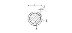
このボールボンディング法による接続において、ボンディングワイヤPには、金線が主に使用されるが、金は高価であるため、近年、銅純度99.99質量%以上の安価な銅線を使用することが行われている。そのとき、銅は裸のままでは、表面の酸化が起こり易いことから、図2に示すように、銅線からなる芯材1に耐酸化金属2を被覆したものが使用されている。
その被覆金属(被覆層)2としては、金(Au)、白金(Pt)、パラジウム(Pd)、銀(Ag)、ニッケル(Ni)等が採用されている(特許文献1〜3)。In the connection by this ball bonding method, a gold wire is mainly used as the bonding wire P. However, since gold is expensive, in recent years, an inexpensive copper wire having a copper purity of 99.99% by mass or more has been used. Has been done. At that time, since the surface is easily oxidized when the copper is bare, as shown in FIG. 2, a
As the coating metal (coating layer) 2, gold (Au), platinum (Pt), palladium (Pd), silver (Ag), nickel (Ni) or the like is employed (
この金属被覆の銅線からなるボンディングワイヤPにおいて、近年の電子部品の小型化等による集積回路素子間の極小化に伴い、上記ボールbもより小さくする必要から、ボンディングワイヤPにも小径のものが望まれ、そのためには、その径Lを50μm以下とするのが好ましいとされている(特許文献1段落0009第12〜14行)。
また、集積回路素子の電極aへの接続において、ボールbが下向き槍状(逆円錐状)になっていると、上記ボールbの電極aへの押付け時、そのボールbの尖鋭端によって電極aを損傷させる恐れがあるため、ボールbはできるだけ、真球であることが好ましい。そのボールbの真球度を高めるために、上記被覆層2の厚みtを芯線径の0.001以下としたり(特許文献1請求項1)、同じく被覆層2の厚みtを0.001〜0.2μmとしたり(特許文献3請求項1)、芯材1の銅よりも高融点の耐酸化金属で被覆層2を形成したりしている(特許文献2段落0014)。
さらに、有機基板をベースにしたBGA(Ball Grid Array)などでは加熱温度(ステージ温度)を高くすると、反りが発生してボンディング性が著しく悪化する。このため、上記ワイヤPと電極a又は導体配線cとの接合時の加熱温度(ステージ温度)を低く、例えば、150℃程度にしても、十分な接合強度を担保するための種々の工夫、例えば、熱処理後に伸線する加工等もされている(特許文献3段落0020、同0054等)。In the bonding wire P made of a metal-coated copper wire, the ball b needs to be made smaller with the miniaturization of integrated circuit elements due to the recent miniaturization of electronic components. For this purpose, the diameter L is preferably 50 μm or less (paragraph 0009, lines 12-14 of Patent Document 1).
In addition, when the ball b is in a downward bowl shape (reverse conical shape) in connection to the electrode a of the integrated circuit element, the electrode b is pressed by the sharp end of the ball b when the ball b is pressed against the electrode a. The ball b is preferably a true sphere as much as possible. In order to increase the sphericity of the ball b, the thickness t of the
Further, in the case of BGA (Ball Grid Array) based on an organic substrate, if the heating temperature (stage temperature) is increased, warping occurs and bonding properties are significantly deteriorated. For this reason, various devices for ensuring sufficient bonding strength, for example, even when the heating temperature (stage temperature) at the time of bonding between the wire P and the electrode a or the conductor wiring c is low, for example, about 150 ° C., In addition, the wire is drawn after the heat treatment (Patent Document 3, paragraphs 0020, 0054, etc.).
以上のように、耐酸化金属で銅線を被覆したボンディングワイヤPは、従来から、種々の工夫がなされてそれなりに好評を得ているが、近年の低コスト化に基づく、作業の高速化に伴う接合強度の向上がさらに要求されている。 As described above, the bonding wire P coated with a copper wire with an oxidation-resistant metal has been well-received as a result of various innovations. However, the work speed has been increased based on the recent cost reduction. There is a further demand for improved joint strength.
この発明はその要求に応えることを課題とする。 This invention makes it a subject to meet the request | requirement.
上記課題を達成するために、この発明は、上記の各工夫を全て採用して、ボンディングワイヤPの線径Lは、12μm以上50.8μm以下とし、純度99.99質量%以上の銅からなる芯材1の外周全面に、金、白金、パラジウム、銀の1種以上による厚みt:0.02〜0.09μmの被覆層2を形成したものとしたのである。 In order to achieve the above object, the present invention adopts all the above-described devices, and the wire diameter L of the bonding wire P is 12 μm or more and 50.8 μm or less, and is made of copper having a purity of 99.99 mass% or more. The
ボンディングワイヤPの線径Lを、50.8μm以下としたのは、上述の特許文献1ではその径Lを50μm以下としているが、50.8μm以下であれば、50μm以下とかわらない程度でもって、上記ボールbをより小さくできるからである。
また、線径Lの下限を12μm以上としたのは、12μm未満ではボンディング前にオペレータがワイヤPをキャピラリー10aに通すのが困難になり、作業性が悪くなるからである。
芯材1の銅純度を99.99質量%以上としたのは、銅の高導電性を担保するためである。The reason why the wire diameter L of the bonding wire P is set to 50.8 μm or less is that the diameter L is set to 50 μm or less in the above-mentioned
The lower limit of the wire diameter L is set to 12 μm or more because if it is less than 12 μm, it becomes difficult for the operator to pass the wire P through the capillary 10a before bonding, resulting in poor workability.
The reason why the copper purity of the
被覆層2の厚みtは薄いほど、ボールbの硬度が低くなり、Siチップ(電極a)の損傷の可能性が低くなるが、薄すぎると、ステッチボンド接合の際に芯材1の銅が露出する度合いが大きくなり、被覆層2を有さない銅ワイヤ程度のステッチボンド接合性しか発現できない。例えば、後記実施例と比較例の実験結果から理解できるように、2回以上のマシンストップが生じる恐れがある。このため、その実施例と比較例の実験結果から、被覆層2の厚みtは0.02μm以上とする。
なお、ステージ温度:150℃程の低温度でのボールボンディングの時には、連続ボンディング性の実験結果からその厚みtを0.04μm以上、より好ましくは、その0.04μmを越えるものとする。ステージ温度を低くすると、ステッチボンド接合に要する加重が大きくなり、被覆層2の厚みtが0.02μm以上から0.04μm未満の範囲では芯材の銅が露出する度合いが大きくなり、連続ボンディング性が損なわれることがあるからである。
一方、被覆層2が厚いと、ボールbの硬度が高くなり、Siチップ(電極a)の損傷の可能性が高くなる。このため、後記実施例と比較例の実験結果から、被覆層2の厚みtは0.09μm以下とする。The thinner the thickness t of the
In the case of ball bonding at a stage temperature as low as about 150 ° C., the thickness t is 0.04 μm or more, more preferably 0.04 μm or more, based on the results of continuous bonding test. When the stage temperature is lowered, the load required for stitch bond bonding increases, and the degree of exposure of the core copper increases when the thickness t of the
On the other hand, if the
被覆金属を金、白金、パラジウム及び銀としたのは、これらの貴金属が電子材料の被覆材として一般的であり、入手が比較的に容易であるからである。これらの純度も芯材1の銅と同様に99.99質量%以上とすることが好ましい。被覆層2はこれらの貴金属の1
つで形成しても良いが、2種以上の金属の多層とすることもできる。The reason why the coating metals are gold, platinum, palladium and silver is that these noble metals are generally used as coating materials for electronic materials and are relatively easy to obtain. Similar to the copper of the
However, it may be a multilayer of two or more metals.
以上から、このボンディングワイヤPの構成としては、集積回路素子の電極aと回路配線基板の導体配線cをボールボンディング法によって接続するための線径L:12μm以上50.8μm以下のボンディングワイヤPにおいて、芯材1が純度99.99質量%以上の銅からなり、その芯材1の外周全面に、金、白金、パラジウム、銀の1種以上による厚み0.02〜0.09μmの被覆層2を形成した構成を採用する。
この構成において、ステージ温度:150℃程の低温度でのボールボンディング用ボンディングワイヤにおいては、その被覆層の厚みtは0.04〜0.09μmとする。From the above, this bonding wire P is configured with a bonding wire P having a diameter L of 12 μm or more and 50.8 μm or less for connecting the electrode a of the integrated circuit element and the conductor wiring c of the circuit wiring board by the ball bonding method. The
In this configuration, in the bonding wire for ball bonding at a stage temperature of as low as about 150 ° C., the thickness t of the coating layer is 0.04 to 0.09 μm.
これらの構成のボンディングワイヤPの製造方法には種々のものが採用できるが、例えば、純度99.99質量%以上の銅からなる芯材1の外周全面に、金、白金、パラジウム、銀の1種以上による被覆層2を形成し、その被覆線を拡散熱処理して芯材と被覆層の密着性を高めた後、線径12μm以上50.8μm以下まで伸線し、さらに、引張伸びが8%以上となるように調質熱処理を行って、被覆層2の厚みt0.02〜0.09μmとした構成を採用できる。 Various methods for manufacturing the bonding wire P having these configurations can be adopted. For example, gold, platinum, palladium, and
これらの構成において、上記被覆層2をその融点が上記銅の融点より高いパラジウム又は白金がより好ましいと考えることができる。
上述のように、芯材1の銅よりも高融点の耐酸化金属で被覆層2を形成すれば、ボールbの真球度が増すことが確認されているが、本発明者は、その理由として、放電によって銅が溶融して真球となる時、その溶融部分が表面張力によって真上にワイヤを這い上がっていくが、被覆層2も溶融していると、その這い上がりが悪くなって、真球になりにくいためと考えた。このことは、0.02〜0.09μm厚の被覆層2であると、顕著に表れる。
また、パラジウムと白金では、パラジウムの方がボールbを真球にできる条件のマージン(限界)が広くなる。これは、パラジウムの融点が白金の融点に比べて銅の融点に近いためと考えられる。すなわち、被覆層2に白金を用いると、放電による銅の溶融後に白金が溶融するまでに時間差が生じるためである。被覆層2にパラジウムを用いれば、溶融の時間差は小さくなるため、より真球になりやすい。In these structures, it can be considered that palladium or platinum having a melting point higher than that of the copper is more preferable for the
As described above, it has been confirmed that if the
Further, in the case of palladium and platinum, the margin of the condition for making the ball b a true sphere becomes wider with palladium. This is considered because the melting point of palladium is closer to the melting point of copper than the melting point of platinum. That is, when platinum is used for the
因みに、上記純銅の融点:1083℃、金の融点:1064℃、パラジウムの融点:1554℃、銀の融点:962℃、白金の融点:1772℃である。
また、被覆層2の厚みtを0.04μm以上とした場合、ステージ温度150℃でもマシントラブルが少なくなるが、特にパラジウムを被覆層2に採用し、被覆層2の厚みtを0.05μm以上とした時にはステージ温度をより低温の135℃としたときでもマシントラブルが起こらないことも確認されている。これは、パラジウム被覆層2の場合、上記のように、銅とパラジウムの溶融時間差が小さく、より真球になりやすいこととの相乗効果に基づくものと考える。Incidentally, the melting point of the pure copper is 1083 ° C., the melting point of gold is 1064 ° C., the melting point of palladium is 1554 ° C., the melting point of silver is 962 ° C., and the melting point of platinum is 1772 ° C.
Further, when the thickness t of the
さらに、上記芯材の銅純度を99.999質量%以上とすれば、後記実施例と比較例の実験結果から理解できるように、Siチップ(電極a)の損傷の可能性が低くなる。これは、銅純度を99.999質量%以上とすることで、FAB硬度をより低減できるからである。 Furthermore, if the copper purity of the core material is 99.999% by mass or more, as can be understood from the experimental results of Examples and Comparative Examples described later, the possibility of damage to the Si chip (electrode a) is reduced. This is because FAB hardness can be reduced more by making copper purity 99.999 mass% or more.
さらに、被覆層2は、電解メッキ、無電解メッキ、蒸着法等の周知の手段によって形成され、一般に、ワイヤPは大きな線径の銅ロッドをダイスと呼ばれるツールに順次貫通させていくことにより、所定の線径に仕上げられるため、この工程途中の適宜な線径で被覆層2を上記手段により形成する。このとき、被覆する際の芯材1の線径は作業性・コストにより決定されるが、製造装置の制限から0.2〜0.8mmが一般的である。外周全面にパラジウム等の金属を被覆された被覆線は200〜500℃(被覆線の温度)で拡散熱処理を施して前記芯材1と被覆層2の密着性を高めた後、線径12μm以上50.8μm以下まで伸線し、さらに、引張伸びが8%以上となるように調質熱処理を行って、被覆層2の厚みt0.02〜0.09μmとすることができる。
引張伸びを8%以上とするのは、ステッチボンド接合性を上げ、より安定したボンディング性を得るためである。
このとき、被覆層がパラジウムから成れば、芯材の銅純度を99.999質量%以上とし、その被覆層の厚みtを0.05〜0.09μmとすることができる。Furthermore, the
The reason why the tensile elongation is 8% or more is to improve the stitch bondability and obtain more stable bonding properties.
At this time, if the coating layer is made of palladium, the copper purity of the core material can be 99.999 mass% or more, and the thickness t of the coating layer can be 0.05 to 0.09 μm.
この発明は、以上のようにしたので、安定した接合強度を有する純銅に貴金属を被覆したボンディングワイヤを得ることができる。 Since the present invention is configured as described above, a bonding wire obtained by coating a noble metal on pure copper having stable bonding strength can be obtained.
表1に示す実施例1〜45及び比較例1〜13を製作し、そのボンディングワイヤPの1st接合部のSiチップ(電極a)の損傷度合、及び連続ボンディング性の試験を行った。
すなわち、まず、銅純度99.99質量%の純銅(表1中:4N)と銅純度99.999質量%の純銅(表1中:5N)の0.2〜0.8mm径の銅線を用意し、その銅線に、Au、Pd、Pt及びAgの貴金属を電解メッキ法によって被覆し、その被覆線を巻き戻し、焼鈍炉を通したのち、再び巻き取り用リールで巻き取ることによって連続拡散熱処理を行った。焼鈍炉は炉長1mの炉芯管を有する電気炉を用い、炉芯管には窒素ガスを流した。その炉温度は500℃以上800℃以下として被覆線の温度を200〜500℃とし、その被覆線の走行速度は5〜60m/分とした。以上の拡散熱処理を施して銅線(芯材)1と被覆層2の密着性を高めた後、線径15〜50.8μmまで伸線し、さらに、引張伸びが8%以上となるように調質熱処理を行って、被覆層2の厚みt:0.001〜0.112μmのボンディングワイヤP(実施例1〜45及び比較例1〜13)を得た。表1中、2種の貴金属を示す例は、その2種の金属を同一厚で2重被覆したものである。Examples 1 to 45 and Comparative Examples 1 to 13 shown in Table 1 were manufactured, and the degree of damage of the Si chip (electrode a) at the first bonding portion of the bonding wire P and the continuous bonding property test were performed.
That is, first, a copper wire having a diameter of 0.2 to 0.8 mm of pure copper having a copper purity of 99.99% by mass (in Table 1: 4N) and pure copper having a copper purity of 99.999% by mass (in Table 1: 5N) is used. Prepare and coat the copper wires with noble metals such as Au, Pd, Pt and Ag by electrolytic plating, rewind the coated wires, pass through an annealing furnace, and then rewind them with a take-up reel. Diffusion heat treatment was performed. As the annealing furnace, an electric furnace having a furnace core tube having a furnace length of 1 m was used, and nitrogen gas was allowed to flow through the furnace core tube. The furnace temperature was 500 ° C. or higher and 800 ° C. or lower, the temperature of the coated wire was 200 to 500 ° C., and the traveling speed of the coated wire was 5 to 60 m / min. After performing the above diffusion heat treatment to improve the adhesion between the copper wire (core material) 1 and the
つぎに、この各ボンディングワイヤPにおいて、下記の評価を行った結果を表1に示す。
「被覆層(表面皮膜層)2の厚み」:
オージェ電子分光分析法にて測定した。Arで被覆層の表面からスパッタリングし、単位時間のスパッタリング毎にスペクトル測定を行った。深さ方向の単位はスパッタ時間とし、事前に測定しておいた標準試料SiO2のスパッタリングレートから、対象材の深さ方向の距離をSiO2換算にて算出した。被覆層については、図3の通り、対象被覆層元素のオージェピーク強度を縦軸、深さを横軸にとったグラフにおいて、オージェピーク強度が84%の位置から16%の位置までの距離を被覆層の厚みとした。
「芯材(銅)の純度」:
GDMS(グロー放電質量)分析にて全元素の濃度を測定してCu純度を決定した。
「連続ボンディング性」(1):
ボンディングマシンで10,000回の連続ボンディングを行い、マシンストップが発生しなければ「A」、1回のマシンストップが発生すれば「B」、2回以上のマシンストップが起これば「D」とした。このとき、ステージ温度が低くなれば、その連続ボンディングが困難になることから、200℃(±5℃)、150℃(±5℃)の2水準で行った。
「1st接合部のSiチップ損傷」(2):
ボンディング後、1stボール接合部直下のSiチップ損傷を評価するために、ボール接合部aおよび電極膜を王水で溶解し、Siチップのクラックを光顕とSEMで観察した。このとき、100個の接合部を観察して5μm以下の微小なピットが1個もしくはまったく見られない場合は「A」、5μm以下の微小なピットが2個以上認められる場合は実用上は有害でないため「B」、5μm以上のクラックが認められた場合は「D」とした。
「総合評価」:
(1)の評価が200℃・150℃ともにAであり、かつ(2)の評価がAのものを「A」、(1)の評価が200℃・150℃ともにAであり、かつ(2)の評価がBのものを「B」、(1)の評価が200℃ではAであり、150℃ではBのものを「C」とした。また、ひとつでもDのあるものについては実用上問題であるので「D」とした。Next, Table 1 shows the results of the following evaluation on each bonding wire P.
“Thickness of coating layer (surface coating layer) 2”:
Measured by Auger electron spectroscopy. Sputtering was performed from the surface of the coating layer with Ar, and the spectrum was measured for each unit time sputtering. The unit in the depth direction was the sputtering time, and the distance in the depth direction of the target material was calculated in terms of SiO2 from the sputtering rate of the standard sample SiO2 measured in advance. For the coating layer, as shown in FIG. 3, in the graph in which the Auger peak intensity of the target coating layer element is on the vertical axis and the depth is on the horizontal axis, the distance from the position where the Auger peak intensity is 84% to the position of 16% is shown. It was set as the thickness of the coating layer.
"Purity of core material (copper)":
Cu purity was determined by measuring the concentration of all elements by GDMS (glow discharge mass) analysis.
“Continuous bonding” (1):
Bonding machine performs 10,000 continuous bonding, "A" if no machine stop occurs, "B" if one machine stop occurs, "D" if more than one machine stop occurs It was. At this time, if the stage temperature is lowered, the continuous bonding becomes difficult. Therefore, it was performed at two levels of 200 ° C. (± 5 ° C.) and 150 ° C. (± 5 ° C.).
“Si chip damage at 1st junction” (2):
After bonding, in order to evaluate the damage of the Si chip directly under the 1st ball joint, the ball joint a and the electrode film were dissolved with aqua regia, and the crack of the Si chip was observed with a light microscope and SEM. At this time, when observing 100 joints and one or more micropits of 5 μm or less are not observed, “A”, and when two or more micropits of 5 μm or less are observed, it is practically harmful. Therefore, “B” and “D” when a crack of 5 μm or more was observed.
"Comprehensive evaluation":
The evaluation of (1) is A for both 200 ° C. and 150 ° C. and the evaluation of (2) is “A”, the evaluation of (1) is A for both 200 ° C. and 150 ° C., and (2 ) Was evaluated as “B” for B, and (1) as A at 200 ° C., and “C” at B at 150 ° C. Moreover, since it is a problem practically about one with D, it was set as "D".

この試験結果から、被覆層厚tが0.02μm未満であると、200℃及び150℃の両連続ボンディング性が低下し(比較例1、2、4、5、9、10、12)、0.02μmに近くなると、前者の連続ボンディング性が満足できるものとなり(比較例2)、0.02μm以上となると、両者の連続ボンディング性が満足できるものとなることが理解できる(実施例1〜45、比較例3、6〜8、11、13)。
一方、被覆層厚tが0.09μmを越えると、ボールbが硬くなって、Siチップ(電極a)の損傷が認められるようになる(比較例3、6〜8、11、13)。
また、純銅5Nを使用し、被覆層厚tを0.04μm以上としたもの(実施例5、12、13、16、20、27、32、34、37、44、45)では、総合評価が「A」となって、ステージ温度が150℃程の低温度においても、連続ボンディング性が良好であってその連続ボンディング性の担保に有効であることが分る。特に、被覆層厚tが0.05μm以上では顕著である(実施例12、13、16)。From this test result, when the coating layer thickness t is less than 0.02 μm, both continuous bonding properties at 200 ° C. and 150 ° C. are reduced (Comparative Examples 1, 2, 4, 5, 9, 10, 12). It can be understood that when the thickness is close to 0.02 μm, the former continuous bonding property is satisfactory (Comparative Example 2), and when it is 0.02 μm or more, both continuous bonding properties are satisfactory (Examples 1 to 45). Comparative Examples 3, 6-8, 11, 13).
On the other hand, when the coating layer thickness t exceeds 0.09 μm, the ball b becomes hard and damage to the Si chip (electrode a) is recognized (Comparative Examples 3, 6-8, 11, 13).
In addition, when pure copper 5N was used and the coating layer thickness t was 0.04 μm or more (Examples 5, 12, 13, 16, 20, 27, 32, 34, 37, 44, 45), the overall evaluation was It can be seen that even when the stage temperature is as low as about 150 ° C., the continuous bonding property is good and effective for ensuring the continuous bonding property. In particular, it is remarkable when the coating layer thickness t is 0.05 μm or more (Examples 12, 13, and 16).
P ボンディングワイヤ
1 芯材
2 被覆層
a 集積回路素子の電極
b ボンディングボール
c 回路配線基板の導体配線
Claims (7)
Translated fromJapanese、芯材(1)が純度99.99質量%以上の銅からなり、その芯材(1)の外周全面に、金、白金、パラジウム、銀の1種以上による厚み(t)0.02〜0.09μmの被覆層(2)を形成したことを特徴とするボンディングワイヤ。A bonding wire (P) having a wire diameter (L) of 12 μm or more and 50.8 μm or less for connecting an electrode (a) of an integrated circuit element and a conductor wiring (c) of a circuit wiring board by a ball bonding method, (1) is made of copper with a purity of 99.99% by mass or more, and the thickness (t) of 0.02 to 0.09 μm is formed on one or more of gold, platinum, palladium and silver on the entire outer periphery of the core material (1). A bonding wire characterized in that a coating layer (2) is formed.
Priority Applications (3)
| Application Number | Priority Date | Filing Date | Title |
|---|---|---|---|
| JP2009094065AJP2010199528A (en) | 2009-01-27 | 2009-04-08 | Bonding wire |
| PCT/JP2009/065735WO2010087053A1 (en) | 2009-01-27 | 2009-09-09 | Bonding wire |
| TW099102279ATW201037777A (en) | 2009-01-27 | 2010-01-27 | Bonding wire |
Applications Claiming Priority (2)
| Application Number | Priority Date | Filing Date | Title |
|---|---|---|---|
| JP2009015265 | 2009-01-27 | ||
| JP2009094065AJP2010199528A (en) | 2009-01-27 | 2009-04-08 | Bonding wire |
Publications (2)
| Publication Number | Publication Date |
|---|---|
| JP2010199528Atrue JP2010199528A (en) | 2010-09-09 |
| JP2010199528A5 JP2010199528A5 (en) | 2011-05-12 |
Family
ID=42395321
Family Applications (1)
| Application Number | Title | Priority Date | Filing Date |
|---|---|---|---|
| JP2009094065APendingJP2010199528A (en) | 2009-01-27 | 2009-04-08 | Bonding wire |
Country Status (3)
| Country | Link |
|---|---|
| JP (1) | JP2010199528A (en) |
| TW (1) | TW201037777A (en) |
| WO (1) | WO2010087053A1 (en) |
Cited By (37)
| Publication number | Priority date | Publication date | Assignee | Title |
|---|---|---|---|---|
| JP2014513439A (en)* | 2011-05-03 | 2014-05-29 | テッセラ,インコーポレイテッド | Package-on-package assembly with wire bond leading to sealing surface |
| US9391008B2 (en) | 2012-07-31 | 2016-07-12 | Invensas Corporation | Reconstituted wafer-level package DRAM |
| US9412714B2 (en) | 2014-05-30 | 2016-08-09 | Invensas Corporation | Wire bond support structure and microelectronic package including wire bonds therefrom |
| US9502390B2 (en) | 2012-08-03 | 2016-11-22 | Invensas Corporation | BVA interposer |
| US9553076B2 (en) | 2010-07-19 | 2017-01-24 | Tessera, Inc. | Stackable molded microelectronic packages with area array unit connectors |
| US9570416B2 (en) | 2004-11-03 | 2017-02-14 | Tessera, Inc. | Stacked packaging improvements |
| US9570382B2 (en) | 2010-07-19 | 2017-02-14 | Tessera, Inc. | Stackable molded microelectronic packages |
| US9583411B2 (en) | 2014-01-17 | 2017-02-28 | Invensas Corporation | Fine pitch BVA using reconstituted wafer with area array accessible for testing |
| US9601454B2 (en) | 2013-02-01 | 2017-03-21 | Invensas Corporation | Method of forming a component having wire bonds and a stiffening layer |
| US9615456B2 (en) | 2012-12-20 | 2017-04-04 | Invensas Corporation | Microelectronic assembly for microelectronic packaging with bond elements to encapsulation surface |
| US9659848B1 (en) | 2015-11-18 | 2017-05-23 | Invensas Corporation | Stiffened wires for offset BVA |
| US9685365B2 (en) | 2013-08-08 | 2017-06-20 | Invensas Corporation | Method of forming a wire bond having a free end |
| US9691679B2 (en) | 2012-02-24 | 2017-06-27 | Invensas Corporation | Method for package-on-package assembly with wire bonds to encapsulation surface |
| US9728527B2 (en) | 2013-11-22 | 2017-08-08 | Invensas Corporation | Multiple bond via arrays of different wire heights on a same substrate |
| US9735084B2 (en) | 2014-12-11 | 2017-08-15 | Invensas Corporation | Bond via array for thermal conductivity |
| US9761558B2 (en) | 2011-10-17 | 2017-09-12 | Invensas Corporation | Package-on-package assembly with wire bond vias |
| US9761554B2 (en) | 2015-05-07 | 2017-09-12 | Invensas Corporation | Ball bonding metal wire bond wires to metal pads |
| US9812402B2 (en) | 2015-10-12 | 2017-11-07 | Invensas Corporation | Wire bond wires for interference shielding |
| US9842745B2 (en) | 2012-02-17 | 2017-12-12 | Invensas Corporation | Heat spreading substrate with embedded interconnects |
| US9852969B2 (en) | 2013-11-22 | 2017-12-26 | Invensas Corporation | Die stacks with one or more bond via arrays of wire bond wires and with one or more arrays of bump interconnects |
| US9888579B2 (en) | 2015-03-05 | 2018-02-06 | Invensas Corporation | Pressing of wire bond wire tips to provide bent-over tips |
| US9911718B2 (en) | 2015-11-17 | 2018-03-06 | Invensas Corporation | ‘RDL-First’ packaged microelectronic device for a package-on-package device |
| US9935075B2 (en) | 2016-07-29 | 2018-04-03 | Invensas Corporation | Wire bonding method and apparatus for electromagnetic interference shielding |
| US9953914B2 (en) | 2012-05-22 | 2018-04-24 | Invensas Corporation | Substrate-less stackable package with wire-bond interconnect |
| US9984992B2 (en) | 2015-12-30 | 2018-05-29 | Invensas Corporation | Embedded wire bond wires for vertical integration with separate surface mount and wire bond mounting surfaces |
| US9984901B2 (en) | 2005-12-23 | 2018-05-29 | Tessera, Inc. | Method for making a microelectronic assembly having conductive elements |
| US10008477B2 (en) | 2013-09-16 | 2018-06-26 | Invensas Corporation | Microelectronic element with bond elements to encapsulation surface |
| US10008469B2 (en) | 2015-04-30 | 2018-06-26 | Invensas Corporation | Wafer-level packaging using wire bond wires in place of a redistribution layer |
| US10026717B2 (en) | 2013-11-22 | 2018-07-17 | Invensas Corporation | Multiple bond via arrays of different wire heights on a same substrate |
| US10181457B2 (en) | 2015-10-26 | 2019-01-15 | Invensas Corporation | Microelectronic package for wafer-level chip scale packaging with fan-out |
| CN109411591A (en)* | 2018-09-14 | 2019-03-01 | 汕头市骏码凯撒有限公司 | A kind of LED encapsulation silver alloy wire and preparation method thereof |
| US10299368B2 (en) | 2016-12-21 | 2019-05-21 | Invensas Corporation | Surface integrated waveguides and circuit structures therefor |
| US10332854B2 (en) | 2015-10-23 | 2019-06-25 | Invensas Corporation | Anchoring structure of fine pitch bva |
| US10381326B2 (en) | 2014-05-28 | 2019-08-13 | Invensas Corporation | Structure and method for integrated circuits packaging with increased density |
| US10460958B2 (en) | 2013-08-07 | 2019-10-29 | Invensas Corporation | Method of manufacturing embedded packaging with preformed vias |
| US10490528B2 (en) | 2015-10-12 | 2019-11-26 | Invensas Corporation | Embedded wire bond wires |
| JP2021093473A (en)* | 2019-12-12 | 2021-06-17 | ローム株式会社 | Semiconductor device and semiconductor device manufacturing method |
Families Citing this family (5)
| Publication number | Priority date | Publication date | Assignee | Title |
|---|---|---|---|---|
| CN102130068B (en)* | 2011-01-07 | 2012-09-05 | 四川威纳尔特种电子材料有限公司 | Alloy-type bonding wire with composite plating on surface |
| JP4860004B1 (en)* | 2011-02-28 | 2012-01-25 | タツタ電線株式会社 | Bonding wire and manufacturing method thereof |
| CN102324392B (en)* | 2011-10-19 | 2013-03-27 | 广东佳博电子科技有限公司 | Preparation process for anti-oxidation copper-based bonding wires |
| CN103219247B (en)* | 2013-03-01 | 2015-11-25 | 溧阳市虹翔机械制造有限公司 | A kind of manufacture method of silver plated bonding copper wire |
| CN103219246B (en)* | 2013-03-01 | 2015-11-25 | 溧阳市虹翔机械制造有限公司 | A kind of manufacture method of plating the silver-plated two coating bonding brass wires of palladium |
Citations (2)
| Publication number | Priority date | Publication date | Assignee | Title |
|---|---|---|---|---|
| JPS6297360A (en)* | 1985-10-24 | 1987-05-06 | Mitsubishi Metal Corp | Surface-coated high-purity copper ultrafine wire for bonding wires for semiconductor devices |
| JP2004064033A (en)* | 2001-10-23 | 2004-02-26 | Sumitomo Electric Wintec Inc | Bonding wire |
Family Cites Families (4)
| Publication number | Priority date | Publication date | Assignee | Title |
|---|---|---|---|---|
| JPS6278863A (en)* | 1985-09-30 | 1987-04-11 | Tanaka Denshi Kogyo Kk | Copper wire for bonding semiconductor devices |
| JPH0786325A (en)* | 1993-09-14 | 1995-03-31 | Hitachi Cable Ltd | Copper wire for electronic equipment |
| KR100739378B1 (en)* | 2000-09-18 | 2007-07-16 | 신닛뽄세이테쯔 카부시키카이샤 | Bonding wire for semiconductor and its manufacturing method |
| JP2003133361A (en)* | 2001-10-23 | 2003-05-09 | Sumiden Magnet Wire Kk | Bonding wire |
- 2009
- 2009-04-08JPJP2009094065Apatent/JP2010199528A/enactivePending
- 2009-09-09WOPCT/JP2009/065735patent/WO2010087053A1/enactiveApplication Filing
- 2010
- 2010-01-27TWTW099102279Apatent/TW201037777A/enunknown
Patent Citations (2)
| Publication number | Priority date | Publication date | Assignee | Title |
|---|---|---|---|---|
| JPS6297360A (en)* | 1985-10-24 | 1987-05-06 | Mitsubishi Metal Corp | Surface-coated high-purity copper ultrafine wire for bonding wires for semiconductor devices |
| JP2004064033A (en)* | 2001-10-23 | 2004-02-26 | Sumitomo Electric Wintec Inc | Bonding wire |
Cited By (66)
| Publication number | Priority date | Publication date | Assignee | Title |
|---|---|---|---|---|
| US9570416B2 (en) | 2004-11-03 | 2017-02-14 | Tessera, Inc. | Stacked packaging improvements |
| US9984901B2 (en) | 2005-12-23 | 2018-05-29 | Tessera, Inc. | Method for making a microelectronic assembly having conductive elements |
| US10128216B2 (en) | 2010-07-19 | 2018-11-13 | Tessera, Inc. | Stackable molded microelectronic packages |
| US9570382B2 (en) | 2010-07-19 | 2017-02-14 | Tessera, Inc. | Stackable molded microelectronic packages |
| US9553076B2 (en) | 2010-07-19 | 2017-01-24 | Tessera, Inc. | Stackable molded microelectronic packages with area array unit connectors |
| US9691731B2 (en) | 2011-05-03 | 2017-06-27 | Tessera, Inc. | Package-on-package assembly with wire bonds to encapsulation surface |
| JP2014513439A (en)* | 2011-05-03 | 2014-05-29 | テッセラ,インコーポレイテッド | Package-on-package assembly with wire bond leading to sealing surface |
| JP2017041643A (en)* | 2011-05-03 | 2017-02-23 | テッセラ,インコーポレイテッド | Package-on-package assembly with wire bond leading to sealing surface |
| US11424211B2 (en) | 2011-05-03 | 2022-08-23 | Tessera Llc | Package-on-package assembly with wire bonds to encapsulation surface |
| US10062661B2 (en) | 2011-05-03 | 2018-08-28 | Tessera, Inc. | Package-on-package assembly with wire bonds to encapsulation surface |
| US10593643B2 (en) | 2011-05-03 | 2020-03-17 | Tessera, Inc. | Package-on-package assembly with wire bonds to encapsulation surface |
| US10756049B2 (en) | 2011-10-17 | 2020-08-25 | Invensas Corporation | Package-on-package assembly with wire bond vias |
| US11735563B2 (en) | 2011-10-17 | 2023-08-22 | Invensas Llc | Package-on-package assembly with wire bond vias |
| US11189595B2 (en) | 2011-10-17 | 2021-11-30 | Invensas Corporation | Package-on-package assembly with wire bond vias |
| US9761558B2 (en) | 2011-10-17 | 2017-09-12 | Invensas Corporation | Package-on-package assembly with wire bond vias |
| US9842745B2 (en) | 2012-02-17 | 2017-12-12 | Invensas Corporation | Heat spreading substrate with embedded interconnects |
| US9691679B2 (en) | 2012-02-24 | 2017-06-27 | Invensas Corporation | Method for package-on-package assembly with wire bonds to encapsulation surface |
| US10170412B2 (en) | 2012-05-22 | 2019-01-01 | Invensas Corporation | Substrate-less stackable package with wire-bond interconnect |
| US9953914B2 (en) | 2012-05-22 | 2018-04-24 | Invensas Corporation | Substrate-less stackable package with wire-bond interconnect |
| US10510659B2 (en) | 2012-05-22 | 2019-12-17 | Invensas Corporation | Substrate-less stackable package with wire-bond interconnect |
| US9917073B2 (en) | 2012-07-31 | 2018-03-13 | Invensas Corporation | Reconstituted wafer-level package dram with conductive interconnects formed in encapsulant at periphery of the package |
| US9391008B2 (en) | 2012-07-31 | 2016-07-12 | Invensas Corporation | Reconstituted wafer-level package DRAM |
| US9502390B2 (en) | 2012-08-03 | 2016-11-22 | Invensas Corporation | BVA interposer |
| US10297582B2 (en) | 2012-08-03 | 2019-05-21 | Invensas Corporation | BVA interposer |
| US9615456B2 (en) | 2012-12-20 | 2017-04-04 | Invensas Corporation | Microelectronic assembly for microelectronic packaging with bond elements to encapsulation surface |
| US9601454B2 (en) | 2013-02-01 | 2017-03-21 | Invensas Corporation | Method of forming a component having wire bonds and a stiffening layer |
| US10460958B2 (en) | 2013-08-07 | 2019-10-29 | Invensas Corporation | Method of manufacturing embedded packaging with preformed vias |
| US9685365B2 (en) | 2013-08-08 | 2017-06-20 | Invensas Corporation | Method of forming a wire bond having a free end |
| US10008477B2 (en) | 2013-09-16 | 2018-06-26 | Invensas Corporation | Microelectronic element with bond elements to encapsulation surface |
| US9728527B2 (en) | 2013-11-22 | 2017-08-08 | Invensas Corporation | Multiple bond via arrays of different wire heights on a same substrate |
| US10629567B2 (en) | 2013-11-22 | 2020-04-21 | Invensas Corporation | Multiple plated via arrays of different wire heights on same substrate |
| US9852969B2 (en) | 2013-11-22 | 2017-12-26 | Invensas Corporation | Die stacks with one or more bond via arrays of wire bond wires and with one or more arrays of bump interconnects |
| US10290613B2 (en) | 2013-11-22 | 2019-05-14 | Invensas Corporation | Multiple bond via arrays of different wire heights on a same substrate |
| US10026717B2 (en) | 2013-11-22 | 2018-07-17 | Invensas Corporation | Multiple bond via arrays of different wire heights on a same substrate |
| USRE49987E1 (en) | 2013-11-22 | 2024-05-28 | Invensas Llc | Multiple plated via arrays of different wire heights on a same substrate |
| US11404338B2 (en) | 2014-01-17 | 2022-08-02 | Invensas Corporation | Fine pitch bva using reconstituted wafer with area array accessible for testing |
| US11990382B2 (en) | 2014-01-17 | 2024-05-21 | Adeia Semiconductor Technologies Llc | Fine pitch BVA using reconstituted wafer with area array accessible for testing |
| US9583411B2 (en) | 2014-01-17 | 2017-02-28 | Invensas Corporation | Fine pitch BVA using reconstituted wafer with area array accessible for testing |
| US10529636B2 (en) | 2014-01-17 | 2020-01-07 | Invensas Corporation | Fine pitch BVA using reconstituted wafer with area array accessible for testing |
| US9837330B2 (en) | 2014-01-17 | 2017-12-05 | Invensas Corporation | Fine pitch BVA using reconstituted wafer with area array accessible for testing |
| US10381326B2 (en) | 2014-05-28 | 2019-08-13 | Invensas Corporation | Structure and method for integrated circuits packaging with increased density |
| US9412714B2 (en) | 2014-05-30 | 2016-08-09 | Invensas Corporation | Wire bond support structure and microelectronic package including wire bonds therefrom |
| US9947641B2 (en) | 2014-05-30 | 2018-04-17 | Invensas Corporation | Wire bond support structure and microelectronic package including wire bonds therefrom |
| US9735084B2 (en) | 2014-12-11 | 2017-08-15 | Invensas Corporation | Bond via array for thermal conductivity |
| US9888579B2 (en) | 2015-03-05 | 2018-02-06 | Invensas Corporation | Pressing of wire bond wire tips to provide bent-over tips |
| US10806036B2 (en) | 2015-03-05 | 2020-10-13 | Invensas Corporation | Pressing of wire bond wire tips to provide bent-over tips |
| US10008469B2 (en) | 2015-04-30 | 2018-06-26 | Invensas Corporation | Wafer-level packaging using wire bond wires in place of a redistribution layer |
| US9761554B2 (en) | 2015-05-07 | 2017-09-12 | Invensas Corporation | Ball bonding metal wire bond wires to metal pads |
| US10115678B2 (en) | 2015-10-12 | 2018-10-30 | Invensas Corporation | Wire bond wires for interference shielding |
| US9812402B2 (en) | 2015-10-12 | 2017-11-07 | Invensas Corporation | Wire bond wires for interference shielding |
| US10490528B2 (en) | 2015-10-12 | 2019-11-26 | Invensas Corporation | Embedded wire bond wires |
| US10559537B2 (en) | 2015-10-12 | 2020-02-11 | Invensas Corporation | Wire bond wires for interference shielding |
| US11462483B2 (en) | 2015-10-12 | 2022-10-04 | Invensas Llc | Wire bond wires for interference shielding |
| US10332854B2 (en) | 2015-10-23 | 2019-06-25 | Invensas Corporation | Anchoring structure of fine pitch bva |
| US10181457B2 (en) | 2015-10-26 | 2019-01-15 | Invensas Corporation | Microelectronic package for wafer-level chip scale packaging with fan-out |
| US9911718B2 (en) | 2015-11-17 | 2018-03-06 | Invensas Corporation | ‘RDL-First’ packaged microelectronic device for a package-on-package device |
| US10043779B2 (en) | 2015-11-17 | 2018-08-07 | Invensas Corporation | Packaged microelectronic device for a package-on-package device |
| US9659848B1 (en) | 2015-11-18 | 2017-05-23 | Invensas Corporation | Stiffened wires for offset BVA |
| US10325877B2 (en) | 2015-12-30 | 2019-06-18 | Invensas Corporation | Embedded wire bond wires for vertical integration with separate surface mount and wire bond mounting surfaces |
| US9984992B2 (en) | 2015-12-30 | 2018-05-29 | Invensas Corporation | Embedded wire bond wires for vertical integration with separate surface mount and wire bond mounting surfaces |
| US10658302B2 (en) | 2016-07-29 | 2020-05-19 | Invensas Corporation | Wire bonding method and apparatus for electromagnetic interference shielding |
| US9935075B2 (en) | 2016-07-29 | 2018-04-03 | Invensas Corporation | Wire bonding method and apparatus for electromagnetic interference shielding |
| US10299368B2 (en) | 2016-12-21 | 2019-05-21 | Invensas Corporation | Surface integrated waveguides and circuit structures therefor |
| CN109411591A (en)* | 2018-09-14 | 2019-03-01 | 汕头市骏码凯撒有限公司 | A kind of LED encapsulation silver alloy wire and preparation method thereof |
| JP2021093473A (en)* | 2019-12-12 | 2021-06-17 | ローム株式会社 | Semiconductor device and semiconductor device manufacturing method |
| JP7412998B2 (en) | 2019-12-12 | 2024-01-15 | ローム株式会社 | Semiconductor device and semiconductor device manufacturing method |
Also Published As
| Publication number | Publication date |
|---|---|
| TW201037777A (en) | 2010-10-16 |
| WO2010087053A1 (en) | 2010-08-05 |
Similar Documents
| Publication | Publication Date | Title |
|---|---|---|
| WO2010087053A1 (en) | Bonding wire | |
| JP5616739B2 (en) | Multilayer copper bonding wire bonding structure | |
| KR101707244B1 (en) | Bonding wire for semiconductor | |
| JP5572121B2 (en) | Bonding wire bonding structure | |
| WO2011129256A1 (en) | Bonding wire | |
| JP4672373B2 (en) | Bonding wires for semiconductor devices | |
| JP2010245390A (en) | Bonding wire | |
| KR101536554B1 (en) | Bonding wire | |
| JP2011146754A5 (en) | ||
| WO2013018238A1 (en) | Ball bonding wire | |
| JP5064577B2 (en) | Ball bonding wire | |
| JP5671512B2 (en) | Bonding wire | |
| JP2004014884A (en) | Bonding wire | |
| JP4722671B2 (en) | Bonding wires for semiconductor devices | |
| JP2006216929A (en) | Bonding wires for semiconductor devices | |
| JP5393614B2 (en) | Bonding wires for semiconductor devices | |
| JP4860004B1 (en) | Bonding wire and manufacturing method thereof | |
| JP5591987B2 (en) | Bonding wires for semiconductor devices | |
| JP5996853B2 (en) | Ball bonding wire | |
| JP2011222882A (en) | Bonding wire | |
| JP2011249463A (en) | Bonding wire | |
| JP5001455B1 (en) | Bonding wire and manufacturing method thereof | |
| JP2013042105A (en) | Bonding wire | |
| JP2010245574A (en) | Bonding wires for semiconductor devices |
Legal Events
| Date | Code | Title | Description |
|---|---|---|---|
| A711 | Notification of change in applicant | Free format text:JAPANESE INTERMEDIATE CODE: A712 Effective date:20100701 | |
| A521 | Written amendment | Free format text:JAPANESE INTERMEDIATE CODE: A523 Effective date:20110325 | |
| A621 | Written request for application examination | Free format text:JAPANESE INTERMEDIATE CODE: A621 Effective date:20110325 | |
| A871 | Explanation of circumstances concerning accelerated examination | Free format text:JAPANESE INTERMEDIATE CODE: A871 Effective date:20110325 | |
| A975 | Report on accelerated examination | Free format text:JAPANESE INTERMEDIATE CODE: A971005 Effective date:20110407 | |
| A131 | Notification of reasons for refusal | Free format text:JAPANESE INTERMEDIATE CODE: A131 Effective date:20110412 | |
| A521 | Written amendment | Free format text:JAPANESE INTERMEDIATE CODE: A523 Effective date:20110510 | |
| A02 | Decision of refusal | Free format text:JAPANESE INTERMEDIATE CODE: A02 Effective date:20110524 |