JP2010192928A - Semiconductor device, and method of manufacturing the same - Google Patents
Semiconductor device, and method of manufacturing the sameDownload PDFInfo
- Publication number
- JP2010192928A JP2010192928AJP2010101251AJP2010101251AJP2010192928AJP 2010192928 AJP2010192928 AJP 2010192928AJP 2010101251 AJP2010101251 AJP 2010101251AJP 2010101251 AJP2010101251 AJP 2010101251AJP 2010192928 AJP2010192928 AJP 2010192928A
- Authority
- JP
- Japan
- Prior art keywords
- wire
- electrode
- pin
- semiconductor device
- semiconductor
- Prior art date
- Legal status (The legal status is an assumption and is not a legal conclusion. Google has not performed a legal analysis and makes no representation as to the accuracy of the status listed.)
- Pending
Links
Images


Classifications
- H—ELECTRICITY
- H01—ELECTRIC ELEMENTS
- H01L—SEMICONDUCTOR DEVICES NOT COVERED BY CLASS H10
- H01L24/00—Arrangements for connecting or disconnecting semiconductor or solid-state bodies; Methods or apparatus related thereto
- H01L24/01—Means for bonding being attached to, or being formed on, the surface to be connected, e.g. chip-to-package, die-attach, "first-level" interconnects; Manufacturing methods related thereto
- H01L24/02—Bonding areas ; Manufacturing methods related thereto
- H01L24/03—Manufacturing methods
- H—ELECTRICITY
- H01—ELECTRIC ELEMENTS
- H01L—SEMICONDUCTOR DEVICES NOT COVERED BY CLASS H10
- H01L24/00—Arrangements for connecting or disconnecting semiconductor or solid-state bodies; Methods or apparatus related thereto
- H01L24/01—Means for bonding being attached to, or being formed on, the surface to be connected, e.g. chip-to-package, die-attach, "first-level" interconnects; Manufacturing methods related thereto
- H01L24/02—Bonding areas ; Manufacturing methods related thereto
- H01L24/04—Structure, shape, material or disposition of the bonding areas prior to the connecting process
- H01L24/05—Structure, shape, material or disposition of the bonding areas prior to the connecting process of an individual bonding area
- H—ELECTRICITY
- H01—ELECTRIC ELEMENTS
- H01L—SEMICONDUCTOR DEVICES NOT COVERED BY CLASS H10
- H01L25/00—Assemblies consisting of a plurality of semiconductor or other solid state devices
- H01L25/03—Assemblies consisting of a plurality of semiconductor or other solid state devices all the devices being of a type provided for in a single subclass of subclasses H10B, H10D, H10F, H10H, H10K or H10N, e.g. assemblies of rectifier diodes
- H01L25/04—Assemblies consisting of a plurality of semiconductor or other solid state devices all the devices being of a type provided for in a single subclass of subclasses H10B, H10D, H10F, H10H, H10K or H10N, e.g. assemblies of rectifier diodes the devices not having separate containers
- H01L25/065—Assemblies consisting of a plurality of semiconductor or other solid state devices all the devices being of a type provided for in a single subclass of subclasses H10B, H10D, H10F, H10H, H10K or H10N, e.g. assemblies of rectifier diodes the devices not having separate containers the devices being of a type provided for in group H10D89/00
- H01L25/0652—Assemblies consisting of a plurality of semiconductor or other solid state devices all the devices being of a type provided for in a single subclass of subclasses H10B, H10D, H10F, H10H, H10K or H10N, e.g. assemblies of rectifier diodes the devices not having separate containers the devices being of a type provided for in group H10D89/00 the devices being arranged next and on each other, i.e. mixed assemblies
- H—ELECTRICITY
- H01—ELECTRIC ELEMENTS
- H01L—SEMICONDUCTOR DEVICES NOT COVERED BY CLASS H10
- H01L25/00—Assemblies consisting of a plurality of semiconductor or other solid state devices
- H01L25/03—Assemblies consisting of a plurality of semiconductor or other solid state devices all the devices being of a type provided for in a single subclass of subclasses H10B, H10D, H10F, H10H, H10K or H10N, e.g. assemblies of rectifier diodes
- H01L25/10—Assemblies consisting of a plurality of semiconductor or other solid state devices all the devices being of a type provided for in a single subclass of subclasses H10B, H10D, H10F, H10H, H10K or H10N, e.g. assemblies of rectifier diodes the devices having separate containers
- H01L25/105—Assemblies consisting of a plurality of semiconductor or other solid state devices all the devices being of a type provided for in a single subclass of subclasses H10B, H10D, H10F, H10H, H10K or H10N, e.g. assemblies of rectifier diodes the devices having separate containers the devices being integrated devices of class H10
- H—ELECTRICITY
- H01—ELECTRIC ELEMENTS
- H01L—SEMICONDUCTOR DEVICES NOT COVERED BY CLASS H10
- H01L2224/00—Indexing scheme for arrangements for connecting or disconnecting semiconductor or solid-state bodies and methods related thereto as covered by H01L24/00
- H01L2224/01—Means for bonding being attached to, or being formed on, the surface to be connected, e.g. chip-to-package, die-attach, "first-level" interconnects; Manufacturing methods related thereto
- H01L2224/02—Bonding areas; Manufacturing methods related thereto
- H01L2224/023—Redistribution layers [RDL] for bonding areas
- H01L2224/0233—Structure of the redistribution layers
- H01L2224/02333—Structure of the redistribution layers being a bump
- H—ELECTRICITY
- H01—ELECTRIC ELEMENTS
- H01L—SEMICONDUCTOR DEVICES NOT COVERED BY CLASS H10
- H01L2224/00—Indexing scheme for arrangements for connecting or disconnecting semiconductor or solid-state bodies and methods related thereto as covered by H01L24/00
- H01L2224/01—Means for bonding being attached to, or being formed on, the surface to be connected, e.g. chip-to-package, die-attach, "first-level" interconnects; Manufacturing methods related thereto
- H01L2224/02—Bonding areas; Manufacturing methods related thereto
- H01L2224/03—Manufacturing methods
- H01L2224/033—Manufacturing methods by local deposition of the material of the bonding area
- H01L2224/0333—Manufacturing methods by local deposition of the material of the bonding area in solid form
- H01L2224/03334—Manufacturing methods by local deposition of the material of the bonding area in solid form using a preform
- H—ELECTRICITY
- H01—ELECTRIC ELEMENTS
- H01L—SEMICONDUCTOR DEVICES NOT COVERED BY CLASS H10
- H01L2224/00—Indexing scheme for arrangements for connecting or disconnecting semiconductor or solid-state bodies and methods related thereto as covered by H01L24/00
- H01L2224/01—Means for bonding being attached to, or being formed on, the surface to be connected, e.g. chip-to-package, die-attach, "first-level" interconnects; Manufacturing methods related thereto
- H01L2224/02—Bonding areas; Manufacturing methods related thereto
- H01L2224/03—Manufacturing methods
- H01L2224/039—Methods of manufacturing bonding areas involving a specific sequence of method steps
- H01L2224/0391—Forming a passivation layer after forming the bonding area
- H—ELECTRICITY
- H01—ELECTRIC ELEMENTS
- H01L—SEMICONDUCTOR DEVICES NOT COVERED BY CLASS H10
- H01L2224/00—Indexing scheme for arrangements for connecting or disconnecting semiconductor or solid-state bodies and methods related thereto as covered by H01L24/00
- H01L2224/01—Means for bonding being attached to, or being formed on, the surface to be connected, e.g. chip-to-package, die-attach, "first-level" interconnects; Manufacturing methods related thereto
- H01L2224/02—Bonding areas; Manufacturing methods related thereto
- H01L2224/04—Structure, shape, material or disposition of the bonding areas prior to the connecting process
- H01L2224/0401—Bonding areas specifically adapted for bump connectors, e.g. under bump metallisation [UBM]
- H—ELECTRICITY
- H01—ELECTRIC ELEMENTS
- H01L—SEMICONDUCTOR DEVICES NOT COVERED BY CLASS H10
- H01L2224/00—Indexing scheme for arrangements for connecting or disconnecting semiconductor or solid-state bodies and methods related thereto as covered by H01L24/00
- H01L2224/01—Means for bonding being attached to, or being formed on, the surface to be connected, e.g. chip-to-package, die-attach, "first-level" interconnects; Manufacturing methods related thereto
- H01L2224/02—Bonding areas; Manufacturing methods related thereto
- H01L2224/04—Structure, shape, material or disposition of the bonding areas prior to the connecting process
- H01L2224/05—Structure, shape, material or disposition of the bonding areas prior to the connecting process of an individual bonding area
- H01L2224/05001—Internal layers
- H01L2224/05005—Structure
- H01L2224/05007—Structure comprising a core and a coating
- H—ELECTRICITY
- H01—ELECTRIC ELEMENTS
- H01L—SEMICONDUCTOR DEVICES NOT COVERED BY CLASS H10
- H01L2224/00—Indexing scheme for arrangements for connecting or disconnecting semiconductor or solid-state bodies and methods related thereto as covered by H01L24/00
- H01L2224/01—Means for bonding being attached to, or being formed on, the surface to be connected, e.g. chip-to-package, die-attach, "first-level" interconnects; Manufacturing methods related thereto
- H01L2224/02—Bonding areas; Manufacturing methods related thereto
- H01L2224/04—Structure, shape, material or disposition of the bonding areas prior to the connecting process
- H01L2224/05—Structure, shape, material or disposition of the bonding areas prior to the connecting process of an individual bonding area
- H01L2224/05001—Internal layers
- H01L2224/0501—Shape
- H01L2224/05016—Shape in side view
- H01L2224/05017—Shape in side view comprising protrusions or indentations
- H—ELECTRICITY
- H01—ELECTRIC ELEMENTS
- H01L—SEMICONDUCTOR DEVICES NOT COVERED BY CLASS H10
- H01L2224/00—Indexing scheme for arrangements for connecting or disconnecting semiconductor or solid-state bodies and methods related thereto as covered by H01L24/00
- H01L2224/01—Means for bonding being attached to, or being formed on, the surface to be connected, e.g. chip-to-package, die-attach, "first-level" interconnects; Manufacturing methods related thereto
- H01L2224/02—Bonding areas; Manufacturing methods related thereto
- H01L2224/04—Structure, shape, material or disposition of the bonding areas prior to the connecting process
- H01L2224/05—Structure, shape, material or disposition of the bonding areas prior to the connecting process of an individual bonding area
- H01L2224/05001—Internal layers
- H01L2224/05099—Material
- H01L2224/051—Material with a principal constituent of the material being a metal or a metalloid, e.g. boron [B], silicon [Si], germanium [Ge], arsenic [As], antimony [Sb], tellurium [Te] and polonium [Po], and alloys thereof
- H01L2224/05138—Material with a principal constituent of the material being a metal or a metalloid, e.g. boron [B], silicon [Si], germanium [Ge], arsenic [As], antimony [Sb], tellurium [Te] and polonium [Po], and alloys thereof the principal constituent melting at a temperature of greater than or equal to 950°C and less than 1550°C
- H01L2224/05144—Gold [Au] as principal constituent
- H—ELECTRICITY
- H01—ELECTRIC ELEMENTS
- H01L—SEMICONDUCTOR DEVICES NOT COVERED BY CLASS H10
- H01L2224/00—Indexing scheme for arrangements for connecting or disconnecting semiconductor or solid-state bodies and methods related thereto as covered by H01L24/00
- H01L2224/01—Means for bonding being attached to, or being formed on, the surface to be connected, e.g. chip-to-package, die-attach, "first-level" interconnects; Manufacturing methods related thereto
- H01L2224/02—Bonding areas; Manufacturing methods related thereto
- H01L2224/04—Structure, shape, material or disposition of the bonding areas prior to the connecting process
- H01L2224/05—Structure, shape, material or disposition of the bonding areas prior to the connecting process of an individual bonding area
- H01L2224/0554—External layer
- H01L2224/0555—Shape
- H01L2224/05556—Shape in side view
- H—ELECTRICITY
- H01—ELECTRIC ELEMENTS
- H01L—SEMICONDUCTOR DEVICES NOT COVERED BY CLASS H10
- H01L2224/00—Indexing scheme for arrangements for connecting or disconnecting semiconductor or solid-state bodies and methods related thereto as covered by H01L24/00
- H01L2224/01—Means for bonding being attached to, or being formed on, the surface to be connected, e.g. chip-to-package, die-attach, "first-level" interconnects; Manufacturing methods related thereto
- H01L2224/02—Bonding areas; Manufacturing methods related thereto
- H01L2224/04—Structure, shape, material or disposition of the bonding areas prior to the connecting process
- H01L2224/05—Structure, shape, material or disposition of the bonding areas prior to the connecting process of an individual bonding area
- H01L2224/0554—External layer
- H01L2224/0556—Disposition
- H01L2224/05568—Disposition the whole external layer protruding from the surface
- H—ELECTRICITY
- H01—ELECTRIC ELEMENTS
- H01L—SEMICONDUCTOR DEVICES NOT COVERED BY CLASS H10
- H01L2224/00—Indexing scheme for arrangements for connecting or disconnecting semiconductor or solid-state bodies and methods related thereto as covered by H01L24/00
- H01L2224/01—Means for bonding being attached to, or being formed on, the surface to be connected, e.g. chip-to-package, die-attach, "first-level" interconnects; Manufacturing methods related thereto
- H01L2224/02—Bonding areas; Manufacturing methods related thereto
- H01L2224/04—Structure, shape, material or disposition of the bonding areas prior to the connecting process
- H01L2224/05—Structure, shape, material or disposition of the bonding areas prior to the connecting process of an individual bonding area
- H01L2224/0554—External layer
- H01L2224/0556—Disposition
- H01L2224/05569—Disposition the external layer being disposed on a redistribution layer on the semiconductor or solid-state body
- H—ELECTRICITY
- H01—ELECTRIC ELEMENTS
- H01L—SEMICONDUCTOR DEVICES NOT COVERED BY CLASS H10
- H01L2224/00—Indexing scheme for arrangements for connecting or disconnecting semiconductor or solid-state bodies and methods related thereto as covered by H01L24/00
- H01L2224/01—Means for bonding being attached to, or being formed on, the surface to be connected, e.g. chip-to-package, die-attach, "first-level" interconnects; Manufacturing methods related thereto
- H01L2224/02—Bonding areas; Manufacturing methods related thereto
- H01L2224/04—Structure, shape, material or disposition of the bonding areas prior to the connecting process
- H01L2224/05—Structure, shape, material or disposition of the bonding areas prior to the connecting process of an individual bonding area
- H01L2224/0554—External layer
- H01L2224/0556—Disposition
- H01L2224/05571—Disposition the external layer being disposed in a recess of the surface
- H01L2224/05572—Disposition the external layer being disposed in a recess of the surface the external layer extending out of an opening
- H—ELECTRICITY
- H01—ELECTRIC ELEMENTS
- H01L—SEMICONDUCTOR DEVICES NOT COVERED BY CLASS H10
- H01L2224/00—Indexing scheme for arrangements for connecting or disconnecting semiconductor or solid-state bodies and methods related thereto as covered by H01L24/00
- H01L2224/01—Means for bonding being attached to, or being formed on, the surface to be connected, e.g. chip-to-package, die-attach, "first-level" interconnects; Manufacturing methods related thereto
- H01L2224/10—Bump connectors; Manufacturing methods related thereto
- H01L2224/11—Manufacturing methods
- H01L2224/113—Manufacturing methods by local deposition of the material of the bump connector
- H01L2224/1133—Manufacturing methods by local deposition of the material of the bump connector in solid form
- H01L2224/1134—Stud bumping, i.e. using a wire-bonding apparatus
- H—ELECTRICITY
- H01—ELECTRIC ELEMENTS
- H01L—SEMICONDUCTOR DEVICES NOT COVERED BY CLASS H10
- H01L2224/00—Indexing scheme for arrangements for connecting or disconnecting semiconductor or solid-state bodies and methods related thereto as covered by H01L24/00
- H01L2224/01—Means for bonding being attached to, or being formed on, the surface to be connected, e.g. chip-to-package, die-attach, "first-level" interconnects; Manufacturing methods related thereto
- H01L2224/10—Bump connectors; Manufacturing methods related thereto
- H01L2224/11—Manufacturing methods
- H01L2224/118—Post-treatment of the bump connector
- H01L2224/1182—Applying permanent coating, e.g. in-situ coating
- H01L2224/11822—Applying permanent coating, e.g. in-situ coating by dipping, e.g. in a solder bath
- H—ELECTRICITY
- H01—ELECTRIC ELEMENTS
- H01L—SEMICONDUCTOR DEVICES NOT COVERED BY CLASS H10
- H01L2224/00—Indexing scheme for arrangements for connecting or disconnecting semiconductor or solid-state bodies and methods related thereto as covered by H01L24/00
- H01L2224/01—Means for bonding being attached to, or being formed on, the surface to be connected, e.g. chip-to-package, die-attach, "first-level" interconnects; Manufacturing methods related thereto
- H01L2224/10—Bump connectors; Manufacturing methods related thereto
- H01L2224/11—Manufacturing methods
- H01L2224/118—Post-treatment of the bump connector
- H01L2224/1183—Reworking, e.g. shaping
- H01L2224/1184—Reworking, e.g. shaping involving a mechanical process, e.g. planarising the bump connector
- H—ELECTRICITY
- H01—ELECTRIC ELEMENTS
- H01L—SEMICONDUCTOR DEVICES NOT COVERED BY CLASS H10
- H01L2224/00—Indexing scheme for arrangements for connecting or disconnecting semiconductor or solid-state bodies and methods related thereto as covered by H01L24/00
- H01L2224/01—Means for bonding being attached to, or being formed on, the surface to be connected, e.g. chip-to-package, die-attach, "first-level" interconnects; Manufacturing methods related thereto
- H01L2224/10—Bump connectors; Manufacturing methods related thereto
- H01L2224/12—Structure, shape, material or disposition of the bump connectors prior to the connecting process
- H01L2224/13—Structure, shape, material or disposition of the bump connectors prior to the connecting process of an individual bump connector
- H01L2224/13001—Core members of the bump connector
- H01L2224/1301—Shape
- H01L2224/13016—Shape in side view
- H01L2224/13017—Shape in side view being non uniform along the bump connector
- H—ELECTRICITY
- H01—ELECTRIC ELEMENTS
- H01L—SEMICONDUCTOR DEVICES NOT COVERED BY CLASS H10
- H01L2224/00—Indexing scheme for arrangements for connecting or disconnecting semiconductor or solid-state bodies and methods related thereto as covered by H01L24/00
- H01L2224/01—Means for bonding being attached to, or being formed on, the surface to be connected, e.g. chip-to-package, die-attach, "first-level" interconnects; Manufacturing methods related thereto
- H01L2224/10—Bump connectors; Manufacturing methods related thereto
- H01L2224/12—Structure, shape, material or disposition of the bump connectors prior to the connecting process
- H01L2224/13—Structure, shape, material or disposition of the bump connectors prior to the connecting process of an individual bump connector
- H01L2224/13001—Core members of the bump connector
- H01L2224/1302—Disposition
- H01L2224/13022—Disposition the bump connector being at least partially embedded in the surface
- H—ELECTRICITY
- H01—ELECTRIC ELEMENTS
- H01L—SEMICONDUCTOR DEVICES NOT COVERED BY CLASS H10
- H01L2224/00—Indexing scheme for arrangements for connecting or disconnecting semiconductor or solid-state bodies and methods related thereto as covered by H01L24/00
- H01L2224/01—Means for bonding being attached to, or being formed on, the surface to be connected, e.g. chip-to-package, die-attach, "first-level" interconnects; Manufacturing methods related thereto
- H01L2224/10—Bump connectors; Manufacturing methods related thereto
- H01L2224/12—Structure, shape, material or disposition of the bump connectors prior to the connecting process
- H01L2224/13—Structure, shape, material or disposition of the bump connectors prior to the connecting process of an individual bump connector
- H01L2224/13001—Core members of the bump connector
- H01L2224/1302—Disposition
- H01L2224/13023—Disposition the whole bump connector protruding from the surface
- H—ELECTRICITY
- H01—ELECTRIC ELEMENTS
- H01L—SEMICONDUCTOR DEVICES NOT COVERED BY CLASS H10
- H01L2224/00—Indexing scheme for arrangements for connecting or disconnecting semiconductor or solid-state bodies and methods related thereto as covered by H01L24/00
- H01L2224/01—Means for bonding being attached to, or being formed on, the surface to be connected, e.g. chip-to-package, die-attach, "first-level" interconnects; Manufacturing methods related thereto
- H01L2224/10—Bump connectors; Manufacturing methods related thereto
- H01L2224/12—Structure, shape, material or disposition of the bump connectors prior to the connecting process
- H01L2224/13—Structure, shape, material or disposition of the bump connectors prior to the connecting process of an individual bump connector
- H01L2224/13001—Core members of the bump connector
- H01L2224/13099—Material
- H01L2224/131—Material with a principal constituent of the material being a metal or a metalloid, e.g. boron [B], silicon [Si], germanium [Ge], arsenic [As], antimony [Sb], tellurium [Te] and polonium [Po], and alloys thereof
- H—ELECTRICITY
- H01—ELECTRIC ELEMENTS
- H01L—SEMICONDUCTOR DEVICES NOT COVERED BY CLASS H10
- H01L2224/00—Indexing scheme for arrangements for connecting or disconnecting semiconductor or solid-state bodies and methods related thereto as covered by H01L24/00
- H01L2224/01—Means for bonding being attached to, or being formed on, the surface to be connected, e.g. chip-to-package, die-attach, "first-level" interconnects; Manufacturing methods related thereto
- H01L2224/10—Bump connectors; Manufacturing methods related thereto
- H01L2224/15—Structure, shape, material or disposition of the bump connectors after the connecting process
- H01L2224/16—Structure, shape, material or disposition of the bump connectors after the connecting process of an individual bump connector
- H01L2224/161—Disposition
- H01L2224/16104—Disposition relative to the bonding area, e.g. bond pad
- H01L2224/16105—Disposition relative to the bonding area, e.g. bond pad the bump connector connecting bonding areas being not aligned with respect to each other
- H—ELECTRICITY
- H01—ELECTRIC ELEMENTS
- H01L—SEMICONDUCTOR DEVICES NOT COVERED BY CLASS H10
- H01L2224/00—Indexing scheme for arrangements for connecting or disconnecting semiconductor or solid-state bodies and methods related thereto as covered by H01L24/00
- H01L2224/01—Means for bonding being attached to, or being formed on, the surface to be connected, e.g. chip-to-package, die-attach, "first-level" interconnects; Manufacturing methods related thereto
- H01L2224/10—Bump connectors; Manufacturing methods related thereto
- H01L2224/15—Structure, shape, material or disposition of the bump connectors after the connecting process
- H01L2224/16—Structure, shape, material or disposition of the bump connectors after the connecting process of an individual bump connector
- H01L2224/161—Disposition
- H01L2224/16135—Disposition the bump connector connecting between different semiconductor or solid-state bodies, i.e. chip-to-chip
- H01L2224/16145—Disposition the bump connector connecting between different semiconductor or solid-state bodies, i.e. chip-to-chip the bodies being stacked
- H—ELECTRICITY
- H01—ELECTRIC ELEMENTS
- H01L—SEMICONDUCTOR DEVICES NOT COVERED BY CLASS H10
- H01L2224/00—Indexing scheme for arrangements for connecting or disconnecting semiconductor or solid-state bodies and methods related thereto as covered by H01L24/00
- H01L2224/01—Means for bonding being attached to, or being formed on, the surface to be connected, e.g. chip-to-package, die-attach, "first-level" interconnects; Manufacturing methods related thereto
- H01L2224/10—Bump connectors; Manufacturing methods related thereto
- H01L2224/15—Structure, shape, material or disposition of the bump connectors after the connecting process
- H01L2224/16—Structure, shape, material or disposition of the bump connectors after the connecting process of an individual bump connector
- H01L2224/161—Disposition
- H01L2224/16151—Disposition the bump connector connecting between a semiconductor or solid-state body and an item not being a semiconductor or solid-state body, e.g. chip-to-substrate, chip-to-passive
- H01L2224/16221—Disposition the bump connector connecting between a semiconductor or solid-state body and an item not being a semiconductor or solid-state body, e.g. chip-to-substrate, chip-to-passive the body and the item being stacked
- H01L2224/16225—Disposition the bump connector connecting between a semiconductor or solid-state body and an item not being a semiconductor or solid-state body, e.g. chip-to-substrate, chip-to-passive the body and the item being stacked the item being non-metallic, e.g. insulating substrate with or without metallisation
- H01L2224/16227—Disposition the bump connector connecting between a semiconductor or solid-state body and an item not being a semiconductor or solid-state body, e.g. chip-to-substrate, chip-to-passive the body and the item being stacked the item being non-metallic, e.g. insulating substrate with or without metallisation the bump connector connecting to a bond pad of the item
- H—ELECTRICITY
- H01—ELECTRIC ELEMENTS
- H01L—SEMICONDUCTOR DEVICES NOT COVERED BY CLASS H10
- H01L2224/00—Indexing scheme for arrangements for connecting or disconnecting semiconductor or solid-state bodies and methods related thereto as covered by H01L24/00
- H01L2224/73—Means for bonding being of different types provided for in two or more of groups H01L2224/10, H01L2224/18, H01L2224/26, H01L2224/34, H01L2224/42, H01L2224/50, H01L2224/63, H01L2224/71
- H01L2224/732—Location after the connecting process
- H01L2224/73201—Location after the connecting process on the same surface
- H01L2224/73203—Bump and layer connectors
- H—ELECTRICITY
- H01—ELECTRIC ELEMENTS
- H01L—SEMICONDUCTOR DEVICES NOT COVERED BY CLASS H10
- H01L2224/00—Indexing scheme for arrangements for connecting or disconnecting semiconductor or solid-state bodies and methods related thereto as covered by H01L24/00
- H01L2224/73—Means for bonding being of different types provided for in two or more of groups H01L2224/10, H01L2224/18, H01L2224/26, H01L2224/34, H01L2224/42, H01L2224/50, H01L2224/63, H01L2224/71
- H01L2224/732—Location after the connecting process
- H01L2224/73251—Location after the connecting process on different surfaces
- H01L2224/73253—Bump and layer connectors
- H—ELECTRICITY
- H01—ELECTRIC ELEMENTS
- H01L—SEMICONDUCTOR DEVICES NOT COVERED BY CLASS H10
- H01L2224/00—Indexing scheme for arrangements for connecting or disconnecting semiconductor or solid-state bodies and methods related thereto as covered by H01L24/00
- H01L2224/74—Apparatus for manufacturing arrangements for connecting or disconnecting semiconductor or solid-state bodies and for methods related thereto
- H01L2224/741—Apparatus for manufacturing means for bonding, e.g. connectors
- H01L2224/742—Apparatus for manufacturing bump connectors
- H—ELECTRICITY
- H01—ELECTRIC ELEMENTS
- H01L—SEMICONDUCTOR DEVICES NOT COVERED BY CLASS H10
- H01L2224/00—Indexing scheme for arrangements for connecting or disconnecting semiconductor or solid-state bodies and methods related thereto as covered by H01L24/00
- H01L2224/74—Apparatus for manufacturing arrangements for connecting or disconnecting semiconductor or solid-state bodies and for methods related thereto
- H01L2224/78—Apparatus for connecting with wire connectors
- H01L2224/7825—Means for applying energy, e.g. heating means
- H01L2224/783—Means for applying energy, e.g. heating means by means of pressure
- H01L2224/78301—Capillary
- H—ELECTRICITY
- H01—ELECTRIC ELEMENTS
- H01L—SEMICONDUCTOR DEVICES NOT COVERED BY CLASS H10
- H01L2224/00—Indexing scheme for arrangements for connecting or disconnecting semiconductor or solid-state bodies and methods related thereto as covered by H01L24/00
- H01L2224/80—Methods for connecting semiconductor or other solid state bodies using means for bonding being attached to, or being formed on, the surface to be connected
- H01L2224/81—Methods for connecting semiconductor or other solid state bodies using means for bonding being attached to, or being formed on, the surface to be connected using a bump connector
- H01L2224/812—Applying energy for connecting
- H01L2224/81201—Compression bonding
- H01L2224/81203—Thermocompression bonding, e.g. diffusion bonding, pressure joining, thermocompression welding or solid-state welding
- H—ELECTRICITY
- H01—ELECTRIC ELEMENTS
- H01L—SEMICONDUCTOR DEVICES NOT COVERED BY CLASS H10
- H01L2224/00—Indexing scheme for arrangements for connecting or disconnecting semiconductor or solid-state bodies and methods related thereto as covered by H01L24/00
- H01L2224/93—Batch processes
- H01L2224/95—Batch processes at chip-level, i.e. with connecting carried out on a plurality of singulated devices, i.e. on diced chips
- H01L2224/96—Batch processes at chip-level, i.e. with connecting carried out on a plurality of singulated devices, i.e. on diced chips the devices being encapsulated in a common layer, e.g. neo-wafer or pseudo-wafer, said common layer being separable into individual assemblies after connecting
- H—ELECTRICITY
- H01—ELECTRIC ELEMENTS
- H01L—SEMICONDUCTOR DEVICES NOT COVERED BY CLASS H10
- H01L2225/00—Details relating to assemblies covered by the group H01L25/00 but not provided for in its subgroups
- H01L2225/03—All the devices being of a type provided for in the same main group of the same subclass of class H10, e.g. assemblies of rectifier diodes
- H01L2225/04—All the devices being of a type provided for in the same main group of the same subclass of class H10, e.g. assemblies of rectifier diodes the devices not having separate containers
- H01L2225/065—All the devices being of a type provided for in the same main group of the same subclass of class H10
- H01L2225/06503—Stacked arrangements of devices
- H01L2225/06513—Bump or bump-like direct electrical connections between devices, e.g. flip-chip connection, solder bumps
- H—ELECTRICITY
- H01—ELECTRIC ELEMENTS
- H01L—SEMICONDUCTOR DEVICES NOT COVERED BY CLASS H10
- H01L2225/00—Details relating to assemblies covered by the group H01L25/00 but not provided for in its subgroups
- H01L2225/03—All the devices being of a type provided for in the same main group of the same subclass of class H10, e.g. assemblies of rectifier diodes
- H01L2225/04—All the devices being of a type provided for in the same main group of the same subclass of class H10, e.g. assemblies of rectifier diodes the devices not having separate containers
- H01L2225/065—All the devices being of a type provided for in the same main group of the same subclass of class H10
- H01L2225/06503—Stacked arrangements of devices
- H01L2225/06517—Bump or bump-like direct electrical connections from device to substrate
- H—ELECTRICITY
- H01—ELECTRIC ELEMENTS
- H01L—SEMICONDUCTOR DEVICES NOT COVERED BY CLASS H10
- H01L2225/00—Details relating to assemblies covered by the group H01L25/00 but not provided for in its subgroups
- H01L2225/03—All the devices being of a type provided for in the same main group of the same subclass of class H10, e.g. assemblies of rectifier diodes
- H01L2225/04—All the devices being of a type provided for in the same main group of the same subclass of class H10, e.g. assemblies of rectifier diodes the devices not having separate containers
- H01L2225/065—All the devices being of a type provided for in the same main group of the same subclass of class H10
- H01L2225/06503—Stacked arrangements of devices
- H01L2225/0652—Bump or bump-like direct electrical connections from substrate to substrate
- H—ELECTRICITY
- H01—ELECTRIC ELEMENTS
- H01L—SEMICONDUCTOR DEVICES NOT COVERED BY CLASS H10
- H01L2225/00—Details relating to assemblies covered by the group H01L25/00 but not provided for in its subgroups
- H01L2225/03—All the devices being of a type provided for in the same main group of the same subclass of class H10, e.g. assemblies of rectifier diodes
- H01L2225/04—All the devices being of a type provided for in the same main group of the same subclass of class H10, e.g. assemblies of rectifier diodes the devices not having separate containers
- H01L2225/065—All the devices being of a type provided for in the same main group of the same subclass of class H10
- H01L2225/06503—Stacked arrangements of devices
- H01L2225/06555—Geometry of the stack, e.g. form of the devices, geometry to facilitate stacking
- H01L2225/06558—Geometry of the stack, e.g. form of the devices, geometry to facilitate stacking the devices having passive surfaces facing each other, i.e. in a back-to-back arrangement
- H—ELECTRICITY
- H01—ELECTRIC ELEMENTS
- H01L—SEMICONDUCTOR DEVICES NOT COVERED BY CLASS H10
- H01L2225/00—Details relating to assemblies covered by the group H01L25/00 but not provided for in its subgroups
- H01L2225/03—All the devices being of a type provided for in the same main group of the same subclass of class H10, e.g. assemblies of rectifier diodes
- H01L2225/04—All the devices being of a type provided for in the same main group of the same subclass of class H10, e.g. assemblies of rectifier diodes the devices not having separate containers
- H01L2225/065—All the devices being of a type provided for in the same main group of the same subclass of class H10
- H01L2225/06503—Stacked arrangements of devices
- H01L2225/06572—Auxiliary carrier between devices, the carrier having an electrical connection structure
- H—ELECTRICITY
- H01—ELECTRIC ELEMENTS
- H01L—SEMICONDUCTOR DEVICES NOT COVERED BY CLASS H10
- H01L2225/00—Details relating to assemblies covered by the group H01L25/00 but not provided for in its subgroups
- H01L2225/03—All the devices being of a type provided for in the same main group of the same subclass of class H10, e.g. assemblies of rectifier diodes
- H01L2225/10—All the devices being of a type provided for in the same main group of the same subclass of class H10, e.g. assemblies of rectifier diodes the devices having separate containers
- H01L2225/1005—All the devices being of a type provided for in the same main group of the same subclass of class H10, e.g. assemblies of rectifier diodes the devices having separate containers the devices being integrated devices of class H10
- H01L2225/1011—All the devices being of a type provided for in the same main group of the same subclass of class H10, e.g. assemblies of rectifier diodes the devices having separate containers the devices being integrated devices of class H10 the containers being in a stacked arrangement
- H01L2225/1017—All the devices being of a type provided for in the same main group of the same subclass of class H10, e.g. assemblies of rectifier diodes the devices having separate containers the devices being integrated devices of class H10 the containers being in a stacked arrangement the lowermost container comprising a device support
- H01L2225/1023—All the devices being of a type provided for in the same main group of the same subclass of class H10, e.g. assemblies of rectifier diodes the devices having separate containers the devices being integrated devices of class H10 the containers being in a stacked arrangement the lowermost container comprising a device support the support being an insulating substrate
- H—ELECTRICITY
- H01—ELECTRIC ELEMENTS
- H01L—SEMICONDUCTOR DEVICES NOT COVERED BY CLASS H10
- H01L2225/00—Details relating to assemblies covered by the group H01L25/00 but not provided for in its subgroups
- H01L2225/03—All the devices being of a type provided for in the same main group of the same subclass of class H10, e.g. assemblies of rectifier diodes
- H01L2225/10—All the devices being of a type provided for in the same main group of the same subclass of class H10, e.g. assemblies of rectifier diodes the devices having separate containers
- H01L2225/1005—All the devices being of a type provided for in the same main group of the same subclass of class H10, e.g. assemblies of rectifier diodes the devices having separate containers the devices being integrated devices of class H10
- H01L2225/1011—All the devices being of a type provided for in the same main group of the same subclass of class H10, e.g. assemblies of rectifier diodes the devices having separate containers the devices being integrated devices of class H10 the containers being in a stacked arrangement
- H01L2225/1047—Details of electrical connections between containers
- H01L2225/1058—Bump or bump-like electrical connections, e.g. balls, pillars, posts
- H—ELECTRICITY
- H01—ELECTRIC ELEMENTS
- H01L—SEMICONDUCTOR DEVICES NOT COVERED BY CLASS H10
- H01L23/00—Details of semiconductor or other solid state devices
- H01L23/28—Encapsulations, e.g. encapsulating layers, coatings, e.g. for protection
- H01L23/31—Encapsulations, e.g. encapsulating layers, coatings, e.g. for protection characterised by the arrangement or shape
- H01L23/3107—Encapsulations, e.g. encapsulating layers, coatings, e.g. for protection characterised by the arrangement or shape the device being completely enclosed
- H01L23/3121—Encapsulations, e.g. encapsulating layers, coatings, e.g. for protection characterised by the arrangement or shape the device being completely enclosed a substrate forming part of the encapsulation
- H01L23/3128—Encapsulations, e.g. encapsulating layers, coatings, e.g. for protection characterised by the arrangement or shape the device being completely enclosed a substrate forming part of the encapsulation the substrate having spherical bumps for external connection
- H—ELECTRICITY
- H01—ELECTRIC ELEMENTS
- H01L—SEMICONDUCTOR DEVICES NOT COVERED BY CLASS H10
- H01L23/00—Details of semiconductor or other solid state devices
- H01L23/28—Encapsulations, e.g. encapsulating layers, coatings, e.g. for protection
- H01L23/31—Encapsulations, e.g. encapsulating layers, coatings, e.g. for protection characterised by the arrangement or shape
- H01L23/3157—Partial encapsulation or coating
- H01L23/3192—Multilayer coating
- H—ELECTRICITY
- H01—ELECTRIC ELEMENTS
- H01L—SEMICONDUCTOR DEVICES NOT COVERED BY CLASS H10
- H01L2924/00—Indexing scheme for arrangements or methods for connecting or disconnecting semiconductor or solid-state bodies as covered by H01L24/00
- H01L2924/0001—Technical content checked by a classifier
- H01L2924/00013—Fully indexed content
- H—ELECTRICITY
- H01—ELECTRIC ELEMENTS
- H01L—SEMICONDUCTOR DEVICES NOT COVERED BY CLASS H10
- H01L2924/00—Indexing scheme for arrangements or methods for connecting or disconnecting semiconductor or solid-state bodies as covered by H01L24/00
- H01L2924/0001—Technical content checked by a classifier
- H01L2924/0002—Not covered by any one of groups H01L24/00, H01L24/00 and H01L2224/00
- H—ELECTRICITY
- H01—ELECTRIC ELEMENTS
- H01L—SEMICONDUCTOR DEVICES NOT COVERED BY CLASS H10
- H01L2924/00—Indexing scheme for arrangements or methods for connecting or disconnecting semiconductor or solid-state bodies as covered by H01L24/00
- H01L2924/01—Chemical elements
- H01L2924/01006—Carbon [C]
- H—ELECTRICITY
- H01—ELECTRIC ELEMENTS
- H01L—SEMICONDUCTOR DEVICES NOT COVERED BY CLASS H10
- H01L2924/00—Indexing scheme for arrangements or methods for connecting or disconnecting semiconductor or solid-state bodies as covered by H01L24/00
- H01L2924/01—Chemical elements
- H01L2924/01029—Copper [Cu]
- H—ELECTRICITY
- H01—ELECTRIC ELEMENTS
- H01L—SEMICONDUCTOR DEVICES NOT COVERED BY CLASS H10
- H01L2924/00—Indexing scheme for arrangements or methods for connecting or disconnecting semiconductor or solid-state bodies as covered by H01L24/00
- H01L2924/013—Alloys
- H01L2924/0132—Binary Alloys
- H01L2924/01322—Eutectic Alloys, i.e. obtained by a liquid transforming into two solid phases
- H—ELECTRICITY
- H01—ELECTRIC ELEMENTS
- H01L—SEMICONDUCTOR DEVICES NOT COVERED BY CLASS H10
- H01L2924/00—Indexing scheme for arrangements or methods for connecting or disconnecting semiconductor or solid-state bodies as covered by H01L24/00
- H01L2924/10—Details of semiconductor or other solid state devices to be connected
- H01L2924/102—Material of the semiconductor or solid state bodies
- H01L2924/1025—Semiconducting materials
- H01L2924/10251—Elemental semiconductors, i.e. Group IV
- H01L2924/10253—Silicon [Si]
- H—ELECTRICITY
- H01—ELECTRIC ELEMENTS
- H01L—SEMICONDUCTOR DEVICES NOT COVERED BY CLASS H10
- H01L2924/00—Indexing scheme for arrangements or methods for connecting or disconnecting semiconductor or solid-state bodies as covered by H01L24/00
- H01L2924/10—Details of semiconductor or other solid state devices to be connected
- H01L2924/11—Device type
- H01L2924/14—Integrated circuits
- H—ELECTRICITY
- H01—ELECTRIC ELEMENTS
- H01L—SEMICONDUCTOR DEVICES NOT COVERED BY CLASS H10
- H01L2924/00—Indexing scheme for arrangements or methods for connecting or disconnecting semiconductor or solid-state bodies as covered by H01L24/00
- H01L2924/15—Details of package parts other than the semiconductor or other solid state devices to be connected
- H01L2924/151—Die mounting substrate
- H01L2924/153—Connection portion
- H01L2924/1531—Connection portion the connection portion being formed only on the surface of the substrate opposite to the die mounting surface
- H01L2924/15311—Connection portion the connection portion being formed only on the surface of the substrate opposite to the die mounting surface being a ball array, e.g. BGA
- H—ELECTRICITY
- H01—ELECTRIC ELEMENTS
- H01L—SEMICONDUCTOR DEVICES NOT COVERED BY CLASS H10
- H01L2924/00—Indexing scheme for arrangements or methods for connecting or disconnecting semiconductor or solid-state bodies as covered by H01L24/00
- H01L2924/15—Details of package parts other than the semiconductor or other solid state devices to be connected
- H01L2924/181—Encapsulation
- H01L2924/1815—Shape
- H01L2924/1816—Exposing the passive side of the semiconductor or solid-state body
- H01L2924/18161—Exposing the passive side of the semiconductor or solid-state body of a flip chip
- H—ELECTRICITY
- H01—ELECTRIC ELEMENTS
- H01L—SEMICONDUCTOR DEVICES NOT COVERED BY CLASS H10
- H01L2924/00—Indexing scheme for arrangements or methods for connecting or disconnecting semiconductor or solid-state bodies as covered by H01L24/00
- H01L2924/15—Details of package parts other than the semiconductor or other solid state devices to be connected
- H01L2924/181—Encapsulation
- H01L2924/1815—Shape
- H01L2924/1816—Exposing the passive side of the semiconductor or solid-state body
- H01L2924/18162—Exposing the passive side of the semiconductor or solid-state body of a chip with build-up interconnect
- H—ELECTRICITY
- H01—ELECTRIC ELEMENTS
- H01L—SEMICONDUCTOR DEVICES NOT COVERED BY CLASS H10
- H01L2924/00—Indexing scheme for arrangements or methods for connecting or disconnecting semiconductor or solid-state bodies as covered by H01L24/00
- H01L2924/30—Technical effects
- H01L2924/35—Mechanical effects
- H01L2924/351—Thermal stress
Landscapes
- Engineering & Computer Science (AREA)
- Power Engineering (AREA)
- Microelectronics & Electronic Packaging (AREA)
- Computer Hardware Design (AREA)
- Physics & Mathematics (AREA)
- Condensed Matter Physics & Semiconductors (AREA)
- General Physics & Mathematics (AREA)
- Manufacturing & Machinery (AREA)
- Structures Or Materials For Encapsulating Or Coating Semiconductor Devices Or Solid State Devices (AREA)
- Wire Bonding (AREA)
Abstract
Description
Translated fromJapanese本発明はピンワイヤを有する半導体装置の製造方法に関する。 The present invention relates to a method for manufacturing a semiconductor device having pin wires.
従来から半導体チップを樹脂で封止してなる半導体パッケージは知られている。半導体パッケージはますます小型化されてきており、最近では半導体チップの大きさとほぼ同じ大きさの半導体パッケージが出現している。このような半導体パッケージは例えばCSP(チップサイズパッケージ)と呼ばれている。 Conventionally, a semiconductor package in which a semiconductor chip is sealed with a resin is known. Semiconductor packages have been increasingly miniaturized, and recently, semiconductor packages having a size almost the same as the size of a semiconductor chip have appeared. Such a semiconductor package is called, for example, a CSP (chip size package).
CSPの製造方法の一つとして、ウエハに集積回路や電極パッド等を形成し、ウエハの電極パッドに接続される柱状電極をウエハに形成し、ウエハの表面及び柱状電極を樹脂で封止し、封止の後でウエハをダイシングして個々の半導体チップを含む半導体パッケージに分離する方法がある(例えば、特開平9−64049号公報)。 As one of CSP manufacturing methods, an integrated circuit, electrode pads, etc. are formed on a wafer, columnar electrodes connected to the electrode pads of the wafer are formed on the wafer, the wafer surface and the columnar electrodes are sealed with resin, There is a method of dicing the wafer after sealing and separating it into semiconductor packages including individual semiconductor chips (for example, Japanese Patent Laid-Open No. 9-64049).
樹脂層は柱状電極の高さとほぼ同じ厚さになるように形成され、柱状電極の先端が樹脂層の表面に露出する。柱状電極に接続される外部端子(電極パッド)が樹脂層の表面に形成され、この外部端子にははんだバンプを取り付けることができる。また、導体パターンからなる再配線導体部分をウエハの表面に形成し、柱状電極の位置をウエハに形成された電極パッドの位置とは異なるように配置することができるようにする。 The resin layer is formed to have substantially the same thickness as the columnar electrode, and the tip of the columnar electrode is exposed on the surface of the resin layer. External terminals (electrode pads) connected to the columnar electrodes are formed on the surface of the resin layer, and solder bumps can be attached to the external terminals. Further, a redistribution conductor portion made of a conductor pattern is formed on the surface of the wafer so that the position of the columnar electrode can be arranged different from the position of the electrode pad formed on the wafer.
また、特開平9−260428号公報(特許文献1)は金属ワイヤを用いて半導体チップを実装基板に実装することを開示している。金属ワイヤの一端は半導体チップの電極パッドにボンディングされ、金属ワイヤの他端ははんだにより実装基板に固定される。この構成によれば、半導体チップと実装基板との熱膨張の差により発生した応力を金属ワイヤのしなりにより吸収することができる。 Japanese Laid-Open Patent Publication No. 9-260428 (Patent Document 1) discloses mounting a semiconductor chip on a mounting substrate using a metal wire. One end of the metal wire is bonded to the electrode pad of the semiconductor chip, and the other end of the metal wire is fixed to the mounting substrate with solder. According to this configuration, the stress generated by the difference in thermal expansion between the semiconductor chip and the mounting substrate can be absorbed by the bending of the metal wire.
半導体装置を回路基板に搭載して使用する場合、半導体装置の外部端子(又ははんだバンプ)が回路基板の電極パッドに接続され、半導体装置の半導体チップと回路基板とが半導体装置の封止樹脂を間に挟んで対向する。使用においては、半導体装置の半導体チップの熱膨張量と実装基板の熱膨張量とが異なっているので、半導体装置の外部端子や柱状電極等に熱応力が発生し、外部端子や柱状電極は繰り返しの熱応力によって疲労する。 When the semiconductor device is mounted on a circuit board and used, the external terminals (or solder bumps) of the semiconductor device are connected to the electrode pads of the circuit board, and the semiconductor chip and the circuit board of the semiconductor device use the sealing resin of the semiconductor device. Opposite it across. In use, the amount of thermal expansion of the semiconductor chip of the semiconductor device is different from the amount of thermal expansion of the mounting substrate. Therefore, thermal stress is generated in the external terminals and columnar electrodes of the semiconductor device, and the external terminals and columnar electrodes are repeated. Fatigue due to thermal stress.
この熱応力は、半導体装置の半導体チップの熱膨張量と回路基板の熱膨張量との差に比例し、封止樹脂層の厚さに反比例する。従って、応力緩和を図るためには、封止樹脂層の厚さを厚くした方がよいことが分かった。しかし、封止樹脂層の厚さを厚くするためには、柱状電極の長さを長くすることが必要である。柱状電極は通常はメッキにより形成されるが、メッキにより形成された柱状電極の長さを長くすることは限られてしまう。 This thermal stress is proportional to the difference between the thermal expansion amount of the semiconductor chip of the semiconductor device and the thermal expansion amount of the circuit board, and inversely proportional to the thickness of the sealing resin layer. Therefore, it was found that the thickness of the sealing resin layer should be increased in order to relax the stress. However, in order to increase the thickness of the sealing resin layer, it is necessary to increase the length of the columnar electrode. The columnar electrode is usually formed by plating, but the length of the columnar electrode formed by plating is limited.
そこで、柱状電極をワイヤ(ボンディングワイヤ)によって形成すると、柱状電極の長さを長くすることができ、よって封止樹脂層の厚さを厚くすることができる。しかし、ワイヤボンダーで処理されるワイヤを柱状電極として用いる場合、ワイヤは柱状電極としては細すぎ、強度が不足することがある。従って、十分な長さ及び強度をもつワイヤで形成された柱状電極を形成することが望まれている。 Therefore, when the columnar electrode is formed of a wire (bonding wire), the length of the columnar electrode can be increased, and thus the thickness of the sealing resin layer can be increased. However, when a wire processed by a wire bonder is used as a columnar electrode, the wire is too thin as a columnar electrode and the strength may be insufficient. Therefore, it is desired to form a columnar electrode formed of a wire having a sufficient length and strength.
さらに、ワイヤは十分に長い柱状電極を提供できるとともにフレキシビリティを備えており、ワイヤからなる柱状電極に熱応力がかかっても柱状電極は破壊されることはない。しかし、半導体装置の封止樹脂層が硬いと、封止樹脂で拘束されたワイヤからなる柱状電極と回路基板に固定された外部端子との間の接合部に大きな応力がかかる。従って、半導体装置の封止樹脂はできるだけ軟らかい樹脂からなるのが好ましい。 Furthermore, the wire can provide a sufficiently long columnar electrode and has flexibility, and the columnar electrode is not broken even if thermal stress is applied to the columnar electrode made of the wire. However, if the sealing resin layer of the semiconductor device is hard, a large stress is applied to the joint between the columnar electrode made of a wire restrained by the sealing resin and the external terminal fixed to the circuit board. Therefore, it is preferable that the sealing resin of the semiconductor device is made of a resin that is as soft as possible.
また、柱状電極の先端を研削したりして調整するときに、ウエハ全体に圧力がかかり、ウエハを損傷してしまうという問題があった。また、樹脂封止の際に、樹脂の流れが柱状電極に望ましくない変形を生じさせることがあった。
他方、近年、半導体装置は、軽く且つ小さいだけでなく高速で作動し、高い機能を備えることを要求されている。半導体チップをインターポーザやマザーボード等の装置に搭載する場合、上記要求を満足するものとして、はんだボールを使用したフリッチチップタイプの搭載方法がある。しかし、この方法では、半導体チップの電極パッド間が狭ピッチであるため、接続に使用されるはんだボールは、ボール径が小さく、バラツキも少ない特別の仕様となり、非常に高価となる。回路面の封止のために使用されるアンダーフィルも、半導体チップとマザーボードの間の狭い隙間を埋めるにあたってボイド等が発生しないことが特性として要求されるため、半導体チップやマザーボードの仕様毎に流れ性や密着性などを改善した特別仕様となる場合が多い。従って、フリップチップタイプの半導体装置は、コストが高くなる。Further, when the tip of the columnar electrode is adjusted by grinding or the like, there is a problem that pressure is applied to the entire wafer and the wafer is damaged. In addition, during resin sealing, the resin flow may cause undesirable deformation of the columnar electrode.
On the other hand, in recent years, semiconductor devices are required not only to be light and small but also to operate at high speed and to have high functions. When a semiconductor chip is mounted on a device such as an interposer or a mother board, there is a flitch chip type mounting method using solder balls to satisfy the above requirements. However, in this method, since the pitch between the electrode pads of the semiconductor chip is narrow, the solder balls used for connection have a special specification with a small ball diameter and little variation, and are very expensive. The underfill used to seal the circuit surface is required to fill the narrow gap between the semiconductor chip and the motherboard so that no voids are generated. It is often a special specification with improved properties and adhesion. Therefore, the cost of the flip chip type semiconductor device is high.
また、導電粒子を内在した接着剤による接合方法や、スタッドバンプを用いた接合方法などがあるが、これらの方法では、半導体チップの反り、ボイド、端子のレベリング精度などにより密着性がバラツクため、信頼性が低く、これらのバラツキ管理のためのコストがアップすることが懸念されている。
フリッチチップタイプの搭載方法においてはんだボールを使用する代わりに、金属ワイヤを使用することが考えられる。金属ワイヤの使用は、自動ワイヤボンダーを使用した従来のワイヤボンディングにおいて発展している。しかし、従来のワイヤボンディングでは、金属ワイヤの先端部を半導体チップの先端に接合し、金属ワイヤの所望の部分をマザーボードの電極に接合した後、キャピラリを動かして金属ワイヤを引っ張ることにより金属ワイヤを切断する。この場合、金属ワイヤは引きちぎられるので、金属ワイヤの切断部は一様な形状にならず、引きちぎられた金属ワイヤの長さも一様にならないという問題があった。In addition, there are a bonding method using an adhesive containing conductive particles, a bonding method using a stud bump, etc., but in these methods, the adhesion varies due to the warping of the semiconductor chip, voids, leveling accuracy of the terminals, etc. There is concern that the reliability is low and the cost for managing these variations increases.
Instead of using solder balls in the flitch chip type mounting method, it is conceivable to use metal wires. The use of metal wires has evolved in conventional wire bonding using automatic wire bonders. However, in the conventional wire bonding, the tip of the metal wire is joined to the tip of the semiconductor chip, the desired portion of the metal wire is joined to the electrode of the motherboard, and then the capillary is moved to pull the metal wire. Disconnect. In this case, since the metal wire is torn, there is a problem that the cut portion of the metal wire does not have a uniform shape, and the length of the torn metal wire does not become uniform.
本発明の目的は熱応力に対して優れた耐久性のあるピンワイヤを有する半導体装置の製造方法を提供することである。 An object of the present invention is to provide a method of manufacturing a semiconductor device having a pin wire having excellent durability against thermal stress.
本発明の特徴による半導体装置の製造方法は、第1端部を有する金属ワイヤに所望の位置でハーフカット処理を行う工程と、該金属ワイヤの第1端部を半導体素子又は半導体装置の電極部にボンディングする工程と、該金属ワイヤを該電極部に対して引っ張ることにより該金属ワイヤを該所望の位置で切断してピンワイヤを形成する工程とを備え、該ピンワイヤは切断された第2端部を有することを特徴とする。 A method of manufacturing a semiconductor device according to a feature of the present invention includes a step of performing a half-cut process on a metal wire having a first end at a desired position, and a first end of the metal wire as a semiconductor element or an electrode portion of a semiconductor device. And cutting the metal wire at the desired position to form a pin wire by pulling the metal wire with respect to the electrode portion, and the pin wire is cut at the second end portion. It is characterized by having.
この構成において、金属ワイヤに所望の位置でハーフカット処理を行い、金属ワイヤの第1端部を半導体素子の電極部にボンディングした後で、金属ワイヤを電極部に対して引っ張ると、金属ワイヤはハーフカットしておいた前記所望の位置で確実に且つきれいに切断される。金属ワイヤの切断部は一様な形状になり、金属ワイヤの長さも一様になる。従って、狭いピッチの複数のピンワイヤを有する半導体素子においては、複数のピンワイヤの高さがほぼ一定になり、半導体素子をマザーボード等の他の装置と接合するの適したものとなる。 In this configuration, when the metal wire is half-cut at a desired position, the first end of the metal wire is bonded to the electrode portion of the semiconductor element, and then the metal wire is pulled with respect to the electrode portion, the metal wire is It is surely and cleanly cut at the desired position that has been half-cut. The cut portion of the metal wire has a uniform shape, and the length of the metal wire is also uniform. Therefore, in a semiconductor element having a plurality of pin wires with a narrow pitch, the height of the plurality of pin wires is substantially constant, and it is suitable for joining the semiconductor element to another device such as a mother board.
以上説明したように、本発明によれば、金属ワイヤの切断部は一様な形状になり、金属ワイヤの長さも一様になる。従って、狭いピッチの複数のピンワイヤを有する半導体素子においては、複数のピンワイヤの高さがほぼ一定になり、半導体素子をマザーボード等の他の装置と接合するの適したものとなる。 As described above, according to the present invention, the cut portion of the metal wire has a uniform shape, and the length of the metal wire is also uniform. Therefore, in a semiconductor element having a plurality of pin wires with a narrow pitch, the height of the plurality of pin wires is substantially constant, and it is suitable for joining the semiconductor element to another device such as a mother board.
以下本発明の実施例について図面を参照して説明する。
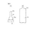
図1は本発明の第1実施例による半導体装置10を示す部分断面斜視図である。図2ははんだボール付着前の図1の半導体装置を示す断面図である。
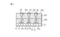
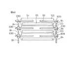
図1及び図2において、半導体装置10は、複数の電極パッド12を有する半導体素子14と、複数の電極パッド12に接続され且つ半導体素子14に対して垂直に延びる複数の柱状電極16と、半導体素子14及び柱状電極16を覆う樹脂層18と、柱状電極16に電気的に接続されるように樹脂層18の表面に配置された外部端子20とを備える。Embodiments of the present invention will be described below with reference to the drawings.
FIG. 1 is a partial cross-sectional perspective view showing a
1 and 2, a
半導体素子14はシリコンチップからなり、集積回路(図示せず)とこの集積回路に適切に接続された電極パッド12を含む。外部端子20は樹脂層18の表面に配置され、柱状電極16の先端に接続、固定されている電極パッドである。さらに、はんだボール20aが外部端子20に接続、固定されている。
樹脂層18は、半導体素子14の表面に形成された柔軟性を有する第1の樹脂層18aと、第1の樹脂層18aよりも半導体素子14から遠い側にあり第1の樹脂層18aよりも高い弾性をもつ第2の樹脂層18bとからなる。第1の樹脂層18aはシリコン系樹脂や低弾性エポキシ系樹脂等からなるヤング率が数〜数100kg/mm2 の低弾性樹脂であり、第2の樹脂層18bは高弾性エポキシ系樹脂等からなるヤング率が1000〜2000kg/mm2 の高弾性樹脂である。The
The
柱状電極16は、半導体素子14の電極パッド12から延び、軸線方向に沿ってほぼ一定の断面積を有するワイヤ部分16aと、外部端子20aから延び且つワイヤ部分16aよりも大きい断面積を有する膨大部分16bとを有する。従って、柱状電極16は、基本的にワイヤによって作られ、長さ及びフレキシビリティを備えるとともに、柱状電極16と外部端子20との接合領域が膨大部分16bを設けることによって強化されている。例えば、柱状電極16は金のワイヤで形成され、柱状電極16のワイヤ部分16aの直径は30〜50μmであり、膨大部分16bの直径はワイヤ部分16aの直径の2〜3倍である。外部端子20の直径は膨大部分16bの直径値〜バンプピッチ×0.5であった。 The
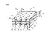
図3は図1の半導体装置10の変形例を示す図である。図1の例と同様に、半導体装置10は、複数の電極パッド12を有する半導体素子14と、複数の電極パッド12に接続された複数の柱状電極16と、半導体素子14及び柱状電極16を覆う樹脂層18と、柱状電極16に電気的に接続されるように樹脂層18の表面に配置された外部端子20とを備える。 FIG. 3 is a view showing a modification of the
柱状電極16は、半導体素子14の電極パッド12から延び、軸線方向に沿ってほぼ一定の断面積を有するワイヤ部分16aと、外部端子20から延び且つワイヤ部分16aよりも大きい断面積を有する膨大部分16bとを有する。従って、柱状電極16は、基本的にワイヤによって作られ、長さ及びフレキシビリティを備えるとともに、柱状電極16と外部端子20との接合領域が膨大部分16bを設けることによって強化されている。 The
この実施例においては、樹脂層18は、半導体素子14の表面に形成された柔軟性を有する第1の樹脂層18aと、第1の樹脂層18aよりも半導体素子14から遠い側にあり第1の樹脂層18aよりも高い弾性をもつ第2の樹脂層18bと、第1の樹脂層18aと第2の樹脂層18bとの間にあってこれらの2つの樹脂層の接着を補助する第3の樹脂層18cとからなる。この例の作用は基本的に図1及び図2の例の作用と同様である。 In this embodiment, the
図4は図1の半導体装置を回路基板に取り付けた例を示す図である。回路基板22は半導体装置10の外部端子20及びはんだボール20aと同じ配列の電極パッド24を有し、半導体装置10は外部端子20(はんだボール20a)を電極パッド24に接合させることにより回路基板22に搭載される。従って、半導体素子14と回路基板22とは樹脂層18を介して対向する。 FIG. 4 is a view showing an example in which the semiconductor device of FIG. 1 is attached to a circuit board. The
使用時には、半導体素子14及び回路基板22は発熱素子の作動によって膨張収縮する。半導体素子14の熱膨張係数と回路基板22の熱膨張係数との差に従って半導体素子14の変形量と回路基板22の変形量との間には差が生じ、柱状電極16及び外部端子20(及びその他の部材)に熱応力が発生する。半導体装置10の外部端子20や柱状電極16は繰り返しの熱応力によって疲労する。 In use, the
しかし、本発明によれば、柱状電極16を基本的にワイヤ部分16aによって構成することによって、長さやフレキシビリティを備え、同時に、膨大部分16bを設けることによって少くとも外部電極20との接合部において十分な強度がある柱状電極16とすることができる。よって、柱状電極16の長さを長く且つ封止樹脂層18の厚さを厚くすることができ、熱疲労に対して優れた耐久性のある半導体装置10を得ることができる。 However, according to the present invention, the
図5は樹脂層18の厚さと外部端子20における応力(バンプ応力)との関係を示す図である。樹脂層18の厚さが厚いほど、外部端子20における応力(バンプ応力)は小さくなる。四角マーク及び菱形マークで示される例は樹脂層18が一層のみであり、その樹脂層の弾性率をAとする。
四角マークで示される例では、外部端子20が0.8mmピッチで配置され、樹脂層18の厚さが100μmのときにバンプ応力が4.3kg/mm2 であった。菱形マークで示される例では、外部端子20が0.5mmピッチで配置され、樹脂層18の厚さが150μmのときにバンプ応力が4.3kg/mm2 となる。FIG. 5 is a diagram showing the relationship between the thickness of the
In the example indicated by the square marks, the bump stress was 4.3 kg / mm2 when the
三角マークで示された例では、第1の樹脂層18aの弾性率を(1/6)Aとし、第2の樹脂層18bの弾性率をAとした。Xマークで示された例では、第1の樹脂層18aの弾性率は(1/6)Aとし、第2の樹脂層18bの弾性率は5Aとした。いずれの場合にも、第1の樹脂層18aの厚さは50μm、第2の樹脂層18bの厚さは100μmであった。今後、端子の微細化がすすんでも、バンプの接合応力は十分に信頼性のあるものを得ることができる。低弾性の第1の樹脂層18aはヤング率が数〜数100kg/mm2のシリコン樹脂または低弾性のエポキシ樹脂とすることができ、高弾性の第2の樹脂層18bはヤング率が1000〜2000kg/mm2の高弾性のエポキシ樹脂とすることができる。In the example indicated by the triangular mark, the elastic modulus of the
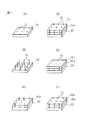
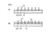
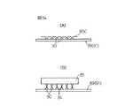
図6は図1から図3の半導体装置10を製造するための方法の例を示す図である。図6(A)はシリコンウエハ30に集積回路や電極パッド12や柱状電極16を形成する工程を示す。図6(B)はシリコンウエハ30に樹脂層18やはんだボール20aを形成した工程を示す。図6(C)ははんだボール20aを形成したシリコンウエハ30を個別の半導体装置10にダイシングする工程を示す図である。図6(D)は分離された半導体装置10を示す図である。図6(A)〜図6(D)から分かるように、本発明による半導体装置10は、シリコンウエハ30の段階で封止用の樹脂層18を形成し、その後で1つの半導体チップを含むチップサイズパッケージ(CSP)として個別の半導体装置10を形成されたものである。従って、封止用の樹脂層18はスピンコートによって塗布されることができるものである。 FIG. 6 is a diagram illustrating an example of a method for manufacturing the
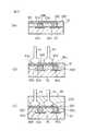
図7は、樹脂層を形成し、それから外部端子に膨大部を形成する工程を含む半導体装置の製造方法の例を示す図である。図7(A)において、ウエハ30に集積回路及び電極パッド12を形成し、図7(B)において、電極パッド12に接続された柱状電極16を形成する。柱状電極16は図1から図3に示されるようにワイヤ部分16aと膨大部分16bとを含む。図7(C)において、第1の樹脂層18aを形成し、図7(D)において、第2の樹脂層18bを形成する。図7(E)において、第2の樹脂層18bを研磨加工し、第2の樹脂層18bから突出する柱状電極16の先端部分を切断する。このとき、柱状電極16の膨大部分16bの先端のみを切断する。それから、図7(E)において、柱状電極16の膨大部分16bの先端に外部端子20を形成する。それから、図6(B)に示されるようにはんだボール20aを形成し、図6(C)に示されるようにしてウエハ30を個々の半導体装置10に切断する。 FIG. 7 is a diagram illustrating an example of a method of manufacturing a semiconductor device including a process of forming a resin layer and then forming a huge portion on an external terminal. 7A, the integrated circuit and the
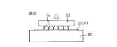
図8は膨大部分を有する柱状電極の形成方法の例を示す図である。この例では、柱状電極16をワイヤボンダーを用いてボンディングワイヤ36によって形成する。ワイヤボンダーは市販のものを利用することができる。図8(A)において、ワイヤボンダーのキャピラリ32をウエハ30の電極パッド12に向かって下降させる。キャピラリ32の先端にはワイヤ材料の小塊34が形成されている。図8(B)において、キャピラリ32をウエハ30に向かってさらに下降させ、キャピラリ32の先端のワイヤ材料の小塊34をウエハ30に接触させる。 FIG. 8 is a diagram showing an example of a method for forming a columnar electrode having a huge portion. In this example, the
図8(C)において、キャピラリ32をウエハ30から引き上げ、ボンディングワイヤ36を形成する。通常のワイヤボンディングにおいては、キャピラリ32がさらに別の電極パッドへ下降され、そこに接触せしめられる。本発明においては、キャピラリ32はウエハ30に対してほぼ垂直にほぼ一定の断面積でまっすぐ引き上げられる。例えば金のワイヤであれば、直径30〜50μmで、高さ500μm程度まで引き上げることができる。 In FIG. 8C, the capillary 32 is pulled up from the
それから、図8(D)において、電気スパーク発生装置38でボンディングワイヤ36に電気スパークを印加すると、ボンディングワイヤ36の一部が小塊状に丸くなる。このとき、電気スパークのエネルギーは、ボンディングワイヤ36が切断されない程度となるように設定する。それから、図8(E)において、ボンディングワイヤ36の先端部の小塊が適当な大きさ(例えば、ボンディングワイヤ36の直径の2〜3倍)になるまで、さらに電気スパークを続けて印加し、最後に、ボンディングワイヤ36が切断される程度のエネルギーで電気スパークを印加する。こうして、図8(F)において、ボンディングワイヤ36は切断され、キャピラリ32を次のポイントへ移動させる。 Then, in FIG. 8D, when the electric spark is applied to the
図9はこうして形成された、ワイヤ部分16aと膨大部分16bとを有する柱状部分16を示す。なお、膨大部分16bに接続される外部端子20の大きさは膨大部分16bの大きさ〜パンプピッチ×0.5程度にする。
図10は膨大部分を有する柱状電極の形成方法の他の例を示す図である。この例でも、柱状電極16をワイヤボンダーを用いてボンディングワイヤによって形成する。図8の例と同様に、図9において、ワイヤボンダーのキャピラリ32をウエハ30の電極パッド12から上方へ持ち上げ、ボンディングワイヤ36を形成する。それから、電気スパーク発生装置38でボンディングワイヤ36に電気スパークを印加する。このとき、電気スパークのエネルギーは、ボンディングワイヤ36の一部が小塊状に丸くなり、かつ、ボンディングワイヤ36が丸くなった小塊において切断される程度となるように設定する。こうして、ワイヤ部分16aと膨大部分16bとを有する柱状部分16が形成される。FIG. 9 shows the
FIG. 10 is a diagram showing another example of a method for forming a columnar electrode having a huge portion. Also in this example, the
図11は、柱状電極16の形成方法の他の例を示す図である。この例では、ワイヤボンダーによってボンディングワイヤ36を形成し、ボンディングワイヤ36の表面にメッキ層40を形成する。例えば、ボンディングワイヤ36は銅であり、50〜100μmmの直径を有する。メッキ層40ははんだのメッキ層であり、その直径はボンディングワイヤ36の直径1.5〜2倍とする。膨大部分16bに接続される外部端子20の大きさは膨大部分16bの大きさ〜パンプピッチ×0.5程度にする。 FIG. 11 is a diagram showing another example of a method for forming the
この例では、ボンディングワイヤ36は、半導体素子14の電極パッド12から延びるワイヤ部分16aとなり、メッキ層40は、外部端子20から延び且つワイヤ部分16aよりも大きい断面積を有する膨大部分16bとなる。この例では、柱状電極16の形成は樹脂層18の形成前に実施され、その後で柱状電極16は樹脂層18によって覆われる。 In this example, the
図12は、柱状電極16の形成方法の他の例を示す図である。図11の例と同様に、この例でも、ワイヤボンダーによってボンディングワイヤ36を形成し、ボンディングワイヤ36の表面にメッキ層40を形成する。ボンディングワイヤ36は、半導体素子14の電極パッド12から延びるワイヤ部分16aとなり、メッキ層40は、外部端子20から延び且つワイヤ部分16aよりも大きい断面積を有する膨大部分16bとなる。この例では、ボンディングワイヤ36の形成は第1の樹脂層18aの形成前に実施され、その後でボンディングワイヤ36は第1の樹脂層18aによって覆われる。メッキ層40は第1の樹脂層18aによって覆われていないボンディングワイヤ36の部分に被覆され、その後で第2の樹脂層18bによって覆われる。 FIG. 12 is a diagram showing another example of a method for forming the
図13は、柱状電極16の形成方法の他の例を示す図である。図11の例と同様に、この例でも、ワイヤボンダーによってボンディングワイヤ36を形成し、ボンディングワイヤ36の表面にメッキ層40を形成する。ボンディングワイヤ36は、半導体素子14の電極パッド12から延びるワイヤ部分16aとなり、メッキ層40は、外部端子20から延び且つワイヤ部分16aよりも大きい断面積を有する膨大部分16bとなる。この例では、樹脂層18は第1〜第3の樹脂層18a、18b、18cを含む。ボンディングワイヤ36の形成は第1の樹脂層18aの形成前に実施され、その後でボンディングワイヤ36は第1及び第3の樹脂層18a、18cによって覆われる。メッキ層40は第1及び第3の樹脂層18a、18cによって覆われていないボンディングワイヤ36の部分に被覆され、その後で第2の樹脂層18bによって覆われる。 FIG. 13 is a diagram showing another example of a method for forming the
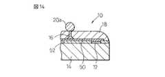
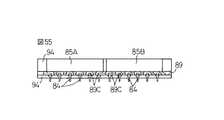
図14は、本発明の第2実施例による半導体装置を示す部分断面図である。半導体装置10は、複数の電極パッド12を有する半導体素子14と、複数の電極パッド12に接続された複数の柱状電極16と、半導体素子14及び柱状電極16を覆う樹脂層18と、柱状電極16に電気的に接続されるように樹脂層18の表面に配置された外部端子としてのはんだボール20aと、半導体素子14の電極パッド12と柱状電極16との間に設けられる再配線導体部分50とを備える。 FIG. 14 is a partial sectional view showing a semiconductor device according to a second embodiment of the present invention. The
絶縁層52が半導体素子14の表面に形成され、電極パッド12は絶縁層52の開口部から露出している。再配線導体部分50は電極パッド12と一対一で対応する電極パッド部分を含む。再配線導体部分50の電極パッド部分は半導体素子14の電極パッド12と電気的に接続され、柱状電極16はその電極パッド部分に固定、接続される。電極パッド12は半導体素子14上の制限された位置に形成されるのに対して、再配線導体部分50の電極パッド部分は所望のパターンで形成されることができる。従って、再配線導体部分50の電極パッド部分は比較的に一様に配置される。従って、樹脂層18にかかる力を特定の柱状電極16と外部端子としてのはんだボール20aの接合部に分散することができる。 An insulating
この実施例でははんだボール20aが外部端子として示されているが、前の実施例と同様に樹脂層18の表面に電極パッドを形成し、その電極パッドを外部端子20とすることができることは言うまでもない。
樹脂層18はスピンコートされた比較的に軟らかい樹脂からなる。逆に言えば、樹脂層18はスピンコートが可能なほどに軟らかいシリコン樹脂又は低弾性のエポキシ樹脂からなる。そして、柱状電極16は主としてボンディングワイヤで形成されている。In this embodiment, the
The
従来の柱状電極はメッキの堆積層として形成されており、大きな厚さにすることが難しいばかりでなく、かなり硬いものであった。そして、従来の封止樹脂層は高弾性の硬いエポキシ樹脂で構成されていた。そのため、硬い柱状電極が硬い封止樹脂層に埋め込まれ、封止樹脂の表面に対向する回路基板が熱ストレスによって封止樹脂に対して動くとき、外部端子が力を受け、その力が柱状電極に伝達されるが、柱状電極は動きにくいために外部端子と柱状電極との接合部が損傷しやすかった。 The conventional columnar electrode is formed as a deposited layer of plating, and is not only difficult to increase in thickness but also very hard. And the conventional sealing resin layer was comprised with the highly elastic hard epoxy resin. Therefore, when the hard columnar electrode is embedded in the hard sealing resin layer and the circuit board facing the surface of the sealing resin moves against the sealing resin due to thermal stress, the external terminal receives a force, and the force is applied to the columnar electrode. However, since the columnar electrode is difficult to move, the joint between the external terminal and the columnar electrode is easily damaged.
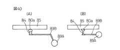
本発明においては、ボンディングワイヤで形成されている柱状電極16自身がフレキシビリティがあり、且つ柱状電極16を取り囲んでいる封止樹脂層18も軟らかくてフレキシビリティがあるので、封止樹脂層18の表面に対向する回路基板が熱ストレスによって封止樹脂層18に対して動くとき、はんだボール20aが力を受け、その力が柱状電極16に伝達されるが、柱状電極16ははんだボール20aの動きに追従して柔軟に動き、はんだボール20aと柱状電極16との接合部が損傷しにくい。 In the present invention, the
図15は図14の半導体装置の変形例を示す図である。この例では、ボンディングワイヤで形成されている柱状電極16が全体的に膨大化されている。この例は、ボンディングワイヤが細すぎる場合に、太い柱状電極16を得るのに有効である。
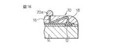
図16は図14の半導体装置の変形例を示す図である。この例では、柱状電極16を構成するボンディングワイヤの端部が、再配線導体部分50に接合され、それから途中で曲がって再び再配線導体部分50に接合され、それから樹脂層18の表面に向かって延びている。この例は、よりフレキシビリティのある柱状電極16を得るのに有効であり、また、再配線導体部分50が断線している場合でも柱状電極16がその断線を補償することができることがある。FIG. 15 is a view showing a modification of the semiconductor device of FIG. In this example, the
FIG. 16 is a view showing a modification of the semiconductor device of FIG. In this example, the end portion of the bonding wire constituting the
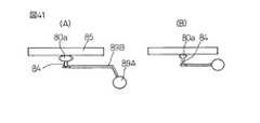
図17(A)は図14の半導体装置の変形例を示す図である。この例では、複数のボンディングワイヤを1つの柱状電極16の形体に接合してなる。この例は、柱状電極16の強度を増大するとともに、フレキシビリティのある柱状電極16を得るのに有効である。図17(B)から図17(D)は図17(A)の柱状電極16の製造工程を示する。図17(B)において、2つのボンディングワイヤ36a、36bが1つの柱状電極16のために形成され、図17(C)において、2つのボンディングワイヤ36a、36bの先端に電気トーチ38aが適用され、よって、図17(D)において、2つのボンディングワイヤ36a、36bの先端が接合される。また、電気トーチ38aの上下動作制御により、多数の柱状電極16の高さを平均化することもできる。 FIG. 17A illustrates a modification of the semiconductor device in FIG. In this example, a plurality of bonding wires are joined to the form of one
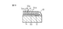
図18は図14の半導体装置の変形例を示す図である。この例では、樹脂層18内に柱状電極16とほぼ平行に配置されたダミー電極54をさらに含む。柱状電極16及びダミー電極54は再配線導体部分50に接合される。柱状電極16の先端がはんだボール20aに接合されるのに対して、ダミー電極54の先端ははんだボール20aに接合されない。従って、ダミー電極54は電気的には働かないが、樹脂層18を形成する際に、樹脂の流れに起因する力が柱状電極16に集中的にかかるのを防止する。 FIG. 18 is a view showing a modification of the semiconductor device of FIG. In this example, the
図19は図18の半導体装置の変形例を示す図である。この例では、樹脂層18内に柱状電極16とほぼ平行に配置されたダミー電極54aをさらに含む。このダミー電極54aは例えばシリコン樹脂や低弾性の樹脂等の樹脂で作られている。ダミー電極54aは、樹脂層18を形成する際に、樹脂の流れに起因する力が柱状電極16に集中的にかかるのを防止し、さらに、樹脂の流れを均等化して樹脂層18の表面が平坦になるのを助ける。 FIG. 19 is a view showing a modification of the semiconductor device of FIG. In this example, the
図20は本発明の第3実施例による半導体装置を示す部分断面図である。半導体装置10は、複数の電極パッド12を有する半導体素子14と、複数の電極パッド12に接続された複数の柱状電極16と、半導体素子14及び柱状電極16を覆う樹脂層18と、柱状電極16と接続して樹脂層18の表面に設けられる再配線導体部分60と、樹脂層18及び再配線導体部分60の一部を覆う絶縁層62と、再配線導体部分60の絶縁層62から露出された部分に電気的に接続される外部端子としてのはんだボール20aとを備えている。この場合にも、はんだボール20aが外部端子として示されているが、前の実施例と同様に樹脂層18の表面に形成された電極パッドを形成し、その電極パッドを外部端子20とすることができることは言うまでもない。 FIG. 20 is a partial sectional view showing a semiconductor device according to a third embodiment of the present invention. The
つまり、この半導体装置10では、半導体素子14の電極パッド12上に柱状電極16が形成され、半導体素子14及び柱状電極16が樹脂層18によって封止された後、再配線導体部分60のパターニングを行い、その後で絶縁層62が形成される。外部端子としてのはんだボール20aは再配線導体部分60と接続されることになる。再配線導体部分60は樹脂層18に覆われていないのでフレキシビリティがあり、再配線導体部分60と外部端子としてのはんだボール20aとの接合部にかかる応力を分散することができる。 That is, in this
図21(A)は図20の半導体装置の変形例を示す図である。半導体装置10は、複数の電極パッド12を有する半導体素子14と、半導体素子14の一部を覆う絶縁層64と、絶縁層64から露出された電極パッド12と接続して絶縁層64の表面に設けられる再配線導体部分60と、絶縁層64及び再配線導体部分60の一部を覆う絶縁層62と、再配線導体部分60の絶縁層62から露出された部分に電気的に接続される外部端子としてのはんだボール20aとを備えている。柱状電極16は、電極パッド12と再配線導体部分60との接合部材66である。 FIG. 21A illustrates a modification of the semiconductor device in FIG. The
つまり、この半導体装置10では、半導体素子14上に絶縁層64が形成され、絶縁層64の電極パッド12上の部分は開口される。それから、絶縁層64の上に再配線導体部分60のパターニングを行い、その後で絶縁層62が形成される。外部端子としてのはんだボール20aは再配線導体部分60と接続されることになる。再配線導体部分60は樹脂層18に覆われていないのでフレキシビリティがあり、再配線導体部分60と外部端子としてのはんだボール20aとの接合部にかかる応力を分散することができる。 That is, in this
図21(B)は電極パッド12と再配線導体部分60との合金層66の形成の例を示す図である。合金層66はアルミニウムと金の共晶合金からなる。表層がアルミニウムの電極パッド12に銅に金メッキした再配線導体部分60を、ボンディングツール68で超音波熱圧着するとアルミニウムと金の共晶合金ができ、合金層66なる。 FIG. 21B is a diagram illustrating an example of formation of the
図21(C)、(D)は電極パッド12と再配線導体部分60との接合部材66の形成の例を示す図である。図21(C)は半導体装置10の断面図、図21(D)は絶縁層64の略平面図である。絶縁層64の電極パッド12上の部分は開口され、その開口部には電極パッド12上にメッキ66aがなされている。このメッキ66aが接合部材66となる。メッキを堆積させるために、電極パッド12上の部分がメッキ浴槽に晒されるように絶縁材をデザインしている。 FIGS. 21C and 21D are diagrams showing an example of forming the
図22は図14から図20の半導体装置の柱状電極の露出方法を示す図である。複数の電極パッド12を有する半導体素子14と、複数の電極パッド12に接続された複数の柱状電極16と、半導体素子14及び柱状電極16を覆う樹脂層18とを備えた半導体装置10においては、樹脂層18をコーティングした直後の状態において、樹脂層18の表面と柱状電極16の先端との関係は、次の2つがある。(a)柱状電極16の先端が樹脂層18の表面よりも突出している(図7)。(b)柱状電極16の先端が樹脂層18の表面とほぼ同じになる。これから説明する例は(b)の場合についてのものである。 FIG. 22 is a view showing a method for exposing the columnar electrodes of the semiconductor devices of FIGS. In the
図22(A)は樹脂層18をコーティングした直後の状態を示し、柱状電極16の先端が樹脂層18の表面とほぼ同じになる。この場合、柱状電極16の先端は樹脂層18の材料の膜が付着しているので、図22(B)に示すように、柱状電極16の先端を外部電極20と電気的に接続するためには、柱状電極16の先端の樹脂層18の材料の膜を除去しなければならない。この場合、樹脂層18の表面全体を除去する必要はなく、樹脂層18の表面のうちで柱状電極16の先端が位置する部分のみを除去すればよい。 FIG. 22A shows a state immediately after coating the
図23は図22の柱状電極の露出方法の一例を示す図である。樹脂層18をコーティングしたウエハ30を持ってきて、ドリルやヤスリ等の工具70を使用して、樹脂層18の表面を、全ての柱状電極16の位置を順番になぞる。すると、柱状電極16の先端の樹脂層18の材料の膜が露出され、柱状電極16の先端が露出される。従って、その後で、柱状電極16の先端に外部電極である電極パッド20を形成したり、はんだボール20aを形成したりすることができる。この方法によれば、樹脂層18の表面全体をグラインダ等で研削する場合と比べて、ウエハ30に大きな力がかからないため、ウエハ30が損傷しない。 FIG. 23 is a diagram showing an example of a method for exposing the columnar electrode of FIG. The
図24は図22の柱状電極の露出方法の一例を示す図である。図24(A)は平面図、図24(B)は側面図である。この例では、紙ヤスリや金属等の無端状の帯部材72が使用される。帯部材72は図24(B)の矢印に沿って回転する。この例では、帯部材72は2つのローラ73に巻きかけられている。金属の帯部材72がリール巻き取り式またはリール一連式になっているようにすることもできる。帯部材72の上方走行部分はウエハ30の上面に接触するように配置され、帯部材72の下方走行部分はウエハの下面の下方に配置される。こうすることによって、樹脂層18の表面の柱状電極16のある部分のみを除去し、柱状電極16の先端が露出されるようにする。従って、この場合にも、樹脂層18の表面全体をグラインダ等で研削する場合と比べて、ウエハ30に大きな力がかからないため、ウエハ30が損傷しない。 FIG. 24 is a diagram showing an example of a method for exposing the columnar electrode of FIG. 24A is a plan view, and FIG. 24B is a side view. In this example, an
図25は図24の柱状電極の露出方法の変形例を示す図である。この例では、帯部材72が使用され、さらに、帯部材72を加熱可能なヒータ74が設けられる。帯部材72を温めることによって、樹脂層18の表面の除去を助ける。
図26は図24の柱状電極の露出方法の変形例を示す図である。この例では、金の電極パッド12に対して、柱状電極16は金の部分16x及びはんだの部分16yを含む構成になっている。銅の帯部材72及びヒータ74が使用される。FIG. 25 is a view showing a modification of the column electrode exposure method of FIG. In this example, a
FIG. 26 is a view showing a modification of the columnar electrode exposure method of FIG. In this example, with respect to the
銅の帯部材72を加熱しながら回転させると、樹脂層18の表面が除去され、且つ銅の帯部材72と柱状電極16のはんだの部分16yとが反応して、柱状電極16のはんだの部分16yが銅の帯部材72に吸着され、よって柱状電極16の先端が露出される。この場合、銅の帯部材72を粗くしたり、フラックスを塗布しておくと、はんだの部分16yをより吸着しやすくなる。また、柱状電極16にフラックスを塗った後、柱状電極16の先端に沿って銅の帯部材72を回転させ、さらにその上部よりはんだ融点より高い熱を加えることにより、銅の帯部材72に柱状電極16のはんだの部分16yを吸着させながら、電極上面を露出させることができる。また、柱状電極16のはんだの部分16yの次の部分を銅にすると、はんだの部分16yには一方において銅の吸着があり且つ他方において銅の吸着があるので、吸着にかかる応力が均等化される。 When the
図27を参照して本発明の第4実施例によるピンワイヤを有する半導体装置の製造する方法について説明する。ピンワイヤは前の実施例の柱状電極16と同様にボンディングワイヤで作られ、柱状電極16と同様に使用されることができる。しかし、この実施例のピンワイヤは前の実施例の柱状電極16よりも種々の応用に使用されることができる。 A method of manufacturing a semiconductor device having pin wires according to the fourth embodiment of the present invention will be described with reference to FIG. The pin wire is made of a bonding wire in the same manner as the
図27(A)において、金属ワイヤ80をキャピラリ81に通す。キャピラリ81は従来的な自動ワイヤボンダーのキャピラリである。金属ワイヤ80はワイヤボンディングで使用される金属、例えば金のワイヤである。キャピラリ81の下側に位置する金属ワイヤ80の下端部分はボール形状の膨大部80aとなっている。膨大部80aは従来的なワイヤボンディングで形成されるのと同様にして例えば加熱や放電等で形成される。 In FIG. 27A, the
図27(B)において、キャピラリ81を矢印に示されるように金属ワイヤ80に対して動かし、キャピラリ81の下端部と金属ワイヤ80の膨大部80aとの間に適切な間隔をあけさせ、金属ワイヤ80の所定の長さ部分を露出させる。
図27(C)において、ハーフカット用工具82は金属ワイヤ80及びキャピラリ81と関連して作動するように配置されている。工具82を作動させ、金属ワイヤ80の所望の位置にハーフカット処理を行い、金属ワイヤ80に物理的な傷をつける。実施例においては、工具82は金属ワイヤ80の両側に配置され、互いに近づき且つ離れるように作動される一対のブレードからなる。In FIG. 27B, the capillary 81 is moved with respect to the
In FIG. 27C, the half-cutting
図28は、ハーフカット処理を行った金属ワイヤ80を示す。金属ワイヤ80にはハーフカット処理を行った位置にウエッジ状の窪み80bが形成される。工具82の位置は金属ワイヤ80から所望の長さのピンワイヤが得られるように設定される。なお、ハーフカット処理を行う工具82は従来的な自動ワイヤボンダーにはなく、本発明を実施するために従来的な自動ワイヤボンダーに付加されたものである。 FIG. 28 shows a
図27(D)において、キャピラリ81を矢印に示されるように元の位置へ動かし、キャピラリ81の下端部を金属ワイヤ80の膨大部80aへ近づける。この状態は、従来的なワイヤボンディングのスタート位置に相当する。さらに、キャピラリ81及び金属ワイヤ80を所望の電子装置の電極部83へ向かって下降させ、キャピラリ81の下端部によって金属ワイヤ80の膨大部80aを電極部83に対して圧着させ、金属ワイヤ80の膨大部80aを電極部83に接合させる。熱圧着時に、従来のワイヤボンディングのように熱又は高周波振動を与えることができる。 In FIG. 27D, the capillary 81 is moved to the original position as shown by the arrow, and the lower end portion of the capillary 81 is brought close to the
図27(E)において、金属ワイヤ80の膨大部80aが電極部83に接合されたら、矢印で示されるようにキャピラリ81を上昇させる。金属ワイヤ80の膨大部80aは電極部83に接合されているので、金属ワイヤ80は動かず、キャピラリ81のみが上昇する。
図27(F)において、キャピラリ81がある距離上昇したら、キャピラリ81に設けられたクランパによってキャピラリ81をクランプし、キャピラリ81をさらに上昇させる。すると、金属ワイヤ80は引っ張られ、ハーフカット処理を行った窪み80bの位置で確実に切断される。こうして、切断された金属ワイヤ80は端部80cを有するピンワイヤ84になる。In FIG. 27E, when the
In FIG. 27F, when the capillary 81 rises by a certain distance, the capillary 81 is clamped by a clamper provided in the capillary 81, and the capillary 81 is further raised. Then, the
図29(A)はこのようにして形成されたピンワイヤ84を示している。図29(B)はピンワイヤ84の一部を拡大して示す。本発明では、ピンワイヤ84は金属ワイヤ80の窪み80bの位置で確実に切断され、得られたピンワイヤ84の長さのバラツキが少ない。また、ハーフカット処理の影響で、ピンワイヤ84の先端がほぼ一定な、安定した突起形状となっている。 FIG. 29A shows the
金属ワイヤ80にハーフカット処理が行われていない金属ワイヤ80の切断の場合には、切断位置が正確に特定されず、金属ワイヤ80の切断部分の形状が一定でなく、ピンワイヤの長さのバラツキが大きくなる。本発明では、機械的なハーフカット処理を施した後で金属ワイヤ80を切断しているので、金属ワイヤ80はハーフカット処理の位置で確実に切断され、長さのバラツキも低減される。また、ハーフカット処理の影響で、ピンワイヤ84の先端がほぼ一定な、中心部が小さく突起した突起形状となっている。先端がフラットな場合と比べ、導電材料との密着面積が広くなり、信頼性の向上が見込める。 In the case of cutting the
図30はピンワイヤ84を有する半導体素子を示す略図である。半導体素子85は半導体チップ又は半導体ウエハからなり、IC回路が形成されている。半導体素子85の表面にはIC回路と接続された電極パッドが形成されている。電極部83は半導体素子85の電極パッドである。ピンワイヤ84は円柱状のピン部80dを有し、ピン部80dの先端側の直径Φaとピン部80dの根元側の直径Φbとはほぼ等しい。ピンワイヤ84の膨大部80aはピン部80dの直径Φa、Φbよりも大きく、ピン部80dの長さtはピン部80dの直径Φa、Φbよりも大きい。 FIG. 30 is a schematic diagram showing a semiconductor device having a
図31は種々のピンワイヤの例を示す図である。ピンワイヤ84Aはピン部80dの直径Φa、Φbが30μmの例である。ピンワイヤ84Bはピン部80dの直径Φa、Φbが50μmの例である。ピンワイヤ84Cはピン部80dの直径Φa、Φbが70μmの例である。このように、金属ワイヤ80を選択することによって、所望の大きさ及び長さ、及び材質のピンワイヤ84Bを得ることができる。 FIG. 31 is a diagram showing examples of various pin wires. The
ピンワイヤ84(84A、84B、84C)を得るための金属ワイヤ80の材質、ワイヤ径(ピン径)、ピン長さ、膨大部80aのサイズには実質的に制限がなく、さらに、フリップチップ用はんだボールやスタッドバンプを使用する場合と比べ、ピンワイヤ84(84A、84B、84C)を非常に低コストで形成することができる。また、ピン部80dの長さを自由に変えることができることから、フィラー径との関係でフリップチップタイプでは使うことが困難とされていたトランスファーモールドによる一括封止も可能になる。 The material of the
図32(A)は図27から図30を参照して説明したピンワイヤ84を有する半導体素子85を示す図である。図30では1つのピンワイヤ84のみが示されているが、図32(A)に示されるように、半導体素子85は通常多数の電極部(電極パッド)83を有し、ピンワイヤ84は各電極部83に接合される。多数のピンワイヤ84は全てほぼ一様な長さを有する。ピンワイヤ84は半導体素子85の表面に対して垂直に、非常に狭いピッチで配置されることができる。ピンワイヤ84は外部端子となる。 FIG. 32A shows the
図32(B)は図32(A)の半導体素子85に樹脂86で樹脂封止を行い、半導体パッケージとした例を示す。ピンワイヤ84は樹脂86の表面から突出して外部端子となる。
図33(A)は再配線技術により形成された再配線電極83Aにピンワイヤ84を接合した半導体素子85を示す図である。この場合にも、多数のピンワイヤ84は全てほぼ一様な長さを有し、外部端子となる。FIG. 32B shows an example in which the
FIG. 33A is a diagram showing a
図33(B)は図33(A)の半導体素子85に樹脂86で樹脂封止を行い、半導体パッケージとした例を示す。ピンワイヤ84は樹脂86の表面から突出して外部端子となる。
図34(A)から図34(C)は再配線電極83Aにピンワイヤ84を接合した半導体素子85の詳細を示す図である。図34(A)において、半導体素子85はIC回路に直接に接続された電極パッド88Aを有し、絶縁層87が半導体素子85を覆って形成される。柱状電極88B及び導電膜88Cが絶縁層87を通って電極パッド88Aに接続され、再配線電極83Aは適切な配置パターンで導電膜88Cに接続される。各再配線電極83Aは各電極パッド88Aに接続されているが、再配線電極83Aの位置は電極パッド88Aの位置とは異なっている。FIG. 33B shows an example in which the
34A to 34C are diagrams showing details of the
図34(B)において、ピンワイヤ84が再配線電極83Aに接合される。図34(C)において、半導体素子85は樹脂86で樹脂封止され、半導体パッケージとなる。
ワイヤボンディング技術を使用したピンワイヤ84の形成は再配線電極(電極部)83Aを含む回路面に与えるダメージが少ないため、ピンワイヤ84は、半導体素子85の電極パッドだけでなく、再配線技術により形成された電極83Aに接合されるのに適している。このため、ピンワイヤ84を有する複数の半導体素子を積み重ねた半導体装置を得ることもできる。さらに、ピン部80dの長さtがピン部80dの直径Φa及びΦbを超えない条件において、ピン部80dの長さtとピン部80dの直径ΦaやΦbは自由に長さや大きさを選択することができる。上記の特徴から、ダメージレス接合やチップスタック化、フレキシブルボンディング、低コストであるトランスファーモールド一括封止などが可能となり、軽量、小型だけでなく高速動作可能で複数の高い機能を備えた半導体装置を低コストで得ることができる。In FIG. 34B, the
Since the formation of the
図35(A)及び図35(B)はピンワイヤ84の変形例を示す図である。図35(A)はピンワイヤ84が屈曲した形状の例を示す。図35(B)はピンワイヤ84が斜めに接合された例を示す。このような変形ピンワイヤ84は半導体素子85側から荷重をかけることによって得られる。このような変形ピンワイヤ84は応力吸収しやすくなる利点がある。 FIG. 35A and FIG. 35B are diagrams showing modifications of the
図36はピンワイヤ84を有する半導体装置の他の例を示す図である。この例では、図32(A)に示される半導体素子85がそれに接合されたピンワイヤ84によってインターポーザ89に搭載されている。ピンワイヤ84は垂直に曲げられ、インターポーザ89の対応する電極(図示せず)との接触面積を増加させるようになっている。さらに、ピンワイヤ84はインターポーザ89の対応する電極との間に導電材料90が配置され、電気的な接続をより確実にしている。なお、ピンワイヤ84は垂直に曲げるのは、半導体素子85をインターポーザ89に対して横方向に動かすことによって達成される。 FIG. 36 is a view showing another example of a semiconductor device having a
図37はピンワイヤ84を有する半導体装置の他の例を示す図である。この例では、図33(B)に示される半導体素子85がそれに接合されたピンワイヤ84によってマザーボード91に搭載されている。ピンワイヤ84は垂直に曲げられ、マザーボード91の対応する電極(図示せず)との接触面積を増加させるようになっている。さらに、ピンワイヤ84はマザーボード91の対応する電極との間に導電材料90が配置され、電気的な接続をより確実にしている。 FIG. 37 is a view showing another example of a semiconductor device having a
図38(A)及び図38(C)はピンワイヤの先端に導電材料を付着させ、インターポーザ又はマザーボードに接着し、熱を加えることによって接合した半導体装置の例を示す図である。図38(A)においては、半導体素子85に設けられたピンワイヤ84を槽90Aの導電材料90に漬けることによって導電材料90を付着させる。図38(B)においては、半導体素子85に設けられたピンワイヤ84を形成板90Bの凹部90Cの導電材料90に漬けることによって導電材料90を付着させる。図38(C)は、ピンワイヤ84及び導電材料90を有する半導体素子85をインターポーザ89又はマザーボード91に搭載するところを示す。図38(B)の方法では導電性材料の濡れ量の管理が容易であるという利点がある。 FIGS. 38A and 38C are diagrams illustrating examples of semiconductor devices in which a conductive material is attached to the tip of a pin wire, bonded to an interposer or a mother board, and bonded by applying heat. In FIG. 38A, the
図39は熱圧着によるピンワイヤの接合の例を示す図である。半導体素子85に設けられたピンワイヤ84をヒータ92上に置かれたインターポーザ89又はマザーボード91に搭載する。半導体素子85には図に矢印で示される力を付加しながら、熱をかけて、ピンワイヤ84をインターポーザ89又はマザーボード91の対応する電極(図示せず)に接合させる。熱圧着による金属結合の場合には接合部の密着性は非常に高い。 FIG. 39 is a diagram showing an example of joining of pin wires by thermocompression bonding. The
図54は印刷によるピンワイヤの接合の例を示す。図54(A)において、印刷マスク90Cを用いて導電材料90をインターポーザ89又はマザーボード91の対応する電極に印刷する。図54(B)において、半導体素子85に設けられたピンワイヤ84を導電材料に接合する。
図40(A)及び図40(B)はピンワイヤ84の直径を変えることによるインピーダンスマッチングの例を示す図である。インターポーザ89はランド89A及びランド89Aからピンワイヤ84に接続される電極まで延びる配線89Bを有する。インターポーザ89側の設計により、配線89Bの長さが変わることがある。図40(A)に示される配線89Bの長さは、図40(B)に示される配線89Bの長さよりも長い。このような場合には、図40(A)に示されるピンワイヤ84の直径を太くし、図40(B)に示されるピンワイヤ84の直径を補足することにより、インピーダンスマッチングを達成することができる。FIG. 54 shows an example of joining of pin wires by printing. In FIG. 54A, the
40A and 40B are diagrams showing an example of impedance matching by changing the diameter of the
図41(A)及び図41(B)はピンワイヤ84の直径を変えることによるインピーダンスマッチングの例を示す図である。この例では、図40(A)に示される長い配線89Bの場合にはピンワイヤ84の膨大部80aの太さを太くし、図40(B)に示される短い配線89Bの場合にはピンワイヤ84の膨大部80aの太さを小さくする。 41A and 41B are diagrams showing an example of impedance matching by changing the diameter of the
このように、数MHz帯の高速半導体デバイスにおいて問題となっている各配線間の信号遅れを低減するために、配線が長い場合には、ワイヤ径を太くしたり、膨大部を大きくしたりして相対的な抵抗値を下げ、各配線間のインピーダンスの値を調整し、信号遅れを少なくする。
図42(A)から図42(E)はメッキ部によりピンワイヤを接合した半導体装置の例を示す図である。図42(A)において、凹部93Aを形成したリードフレーム93を準備し、図42(B)において、凹部93Aの表面にメッキしてメッキ部93Bを形成する。図42(C)において、半導体素子85のピンワイヤ84の先端をメッキ部93Bに接合する。熱圧着により、ピンワイヤ84の先端はメッキ部93Bに簡単に接合する。図42(D)において、半導体素子85を樹脂94により樹脂封止する。樹脂94は半導体素子85とリードフレーム93との間の空間を埋める。それから、図42(E)において、リードフレーム93を化学的なエッチングにより溶かし、メッキ部93Bを露出させる。メッキ部93Bはピンワイヤ84の先端に付着している。このようにして、メッキ部93Bはピンワイヤ84とともに外部端子となる。この技術はフェイスアップタイプのBCC(Bump Chip Carrier )パッケージと比較して、小型化、ファインピッチ化、高速化を実現できる。In this way, in order to reduce the signal delay between each wiring, which is a problem in high-speed semiconductor devices of several MHz band, when the wiring is long, the wire diameter is increased or the enormous part is increased. Reduce the relative resistance value, adjust the impedance value between each wiring, and reduce the signal delay.
FIG. 42A to FIG. 42E are diagrams showing examples of a semiconductor device in which a pin wire is joined by a plating portion. 42A, a
図43はピンワイヤを有する半導体装置の一例を示す図である。図43(A)は、図38、図39又は図54に示されるように半導体素子85が導電材料90を付着させたピンワイヤ84によりインターポーザ89に搭載された例を示す。図43(B)は図43(A)に示される半導体装置にトランスファーモールドする例を示す。樹脂94を金型95に流し込む。ピンワイヤ84が高い密度で配置されている場合でも、トランスファーモールドを行うことができる。図43(C)においては、金型95を除去し、インターポーザ89の反対面側に金属ボール96を接合して、半導体パッケージを完成する。 FIG. 43 is a diagram illustrating an example of a semiconductor device having a pin wire. FIG. 43A shows an example in which the
図44は樹脂封止の他の例を示す図である。図43(B)のトランスファーモールドの代わりに、図44に示されるようにポッティングにより樹脂封止を行うこともできる。
図45は半導体装置の一例を示す平面図である。図46は図45の平面的に配置された複数の半導体素子を含む半導体装置の例を示す図である。図45(A)及び図46(A)において、それぞれにピンワイヤ84を有する複数の半導体素子85が金属板97に平面的に配置される。ピンワイヤ84には導電材料90を付着させてある。複数の半導体素子85は接着剤98によって金属板97に固定される。図46(B)において、複数の半導体素子85はピンワイヤ84によりインターポーザ89に搭載される。図46(C)において、半導体素子85を樹脂94により樹脂封止し、インターポーザ89の反対面側に金属ボール96を接合して、半導体パッケージを完成する。図45(B)は金属ボール96の配置を示している。FIG. 44 is a diagram showing another example of resin sealing. Instead of the transfer mold of FIG. 43B, resin sealing can also be performed by potting as shown in FIG.
FIG. 45 is a plan view showing an example of a semiconductor device. FIG. 46 is a diagram showing an example of a semiconductor device including a plurality of semiconductor elements arranged in a plane in FIG. 45A and 46A, a plurality of
図47は立体的に配置された複数の半導体素子85を含む半導体装置の例を示す図である。この例では、半導体素子85Aの回路面側と半導体素子85Bの背面側は接着材により固定、接着され、これらの半導体素子85A、85Bはそれぞれにピンワイヤ84を有する。半導体素子85A、85Bはピンワイヤ84によりインターポーザ89に搭載される。半導体素子85A、85Bを樹脂94により樹脂封止し、インターポーザ89の反対面側に金属ボール96を接合して、半導体パッケージを完成する。 FIG. 47 is a diagram showing an example of a semiconductor device including a plurality of
図48は立体的に配置された複数の半導体素子を含む半導体装置の例を示す図である。この例では、半導体素子85Aはピンワイヤ84及び例えば図34(C)に示される再配線電極83Aを有し、それぞれにピンワイヤ84を有する半導体素子85Bと半導体素子85Cとは背中合わせで互いに固定される。半導体素子85Bのピンワイヤ84は半導体素子85Aの再配線電極83Aに接合される。一方、半導体素子85A、85Bはピンワイヤ84によりインターポーザ89に搭載される。半導体素子85A、85Bを樹脂94により樹脂封止し、インターポーザ89の反対面側に金属ボール96を接合して、半導体パッケージを完成する。 FIG. 48 is a diagram illustrating an example of a semiconductor device including a plurality of semiconductor elements arranged in three dimensions. In this example, the
図49はスタックとして立体的に配置された複数の半導体装置を含む半導体装置の例を示す図である。参照数字100は半導体素子85と、インターポーザ89と、半導体素子85とインターポーザ89とを樹脂封止する樹脂94とからなる半導体装置(半導体パッケージ)を示す。半導体素子85とインターポーザ89とは、図示しない適切な導体により接続される。 FIG. 49 is a diagram illustrating an example of a semiconductor device including a plurality of semiconductor devices arranged three-dimensionally as a stack.
図49においては、3つの半導体装置(半導体パッケージ)100がスタックとして立体的に配置されている。各インターポーザ89は樹脂94から横方向に延びだし、インターポーザ89の延びだした部分は電極部83Bを有し、その電極部83Bにはピンワイヤ84が接合されている。ピンワイヤ84の電極部83Bへの接合は上記したのと同様にして行われる。上下関係で隣接する2つの半導体装置(半導体パッケージ)100はピンワイヤ84によって接続されている。このように、パッケージとパッケージを積み重ねる際の接続端子としてピンワイヤを適用すると、従来技術よりも伝送経路の短縮が図れるため高速伝送に非常に有利となる。 In FIG. 49, three semiconductor devices (semiconductor packages) 100 are three-dimensionally arranged as a stack. Each
図50はスタックとして形成された立体的に配置された複数の半導体素子を含む半導体装置の例を示す図である。図50においては、3つの半導体装置(半導体パッケージ)100がスタックとして立体的に配置されている。図50では各半導体装置(半導体パッケージ)100の半導体素子85とインターポーザ89とがピンワイヤ84によって接合され、そして、インターポーザ89の延びだした部分にもピンワイヤ84が接合されている。このようにして、ピンワイヤ84は各半導体装置(半導体パッケージ)100内に配置されるばかりでなく、隣接する2つの半導体装置(半導体パッケージ)100を接続する。 FIG. 50 is a diagram illustrating an example of a semiconductor device including a plurality of three-dimensionally arranged semiconductor elements formed as a stack. In FIG. 50, three semiconductor devices (semiconductor packages) 100 are three-dimensionally arranged as a stack. In FIG. 50, the
以上に説明した半導体素子53及び半導体装置及び半導体パッケージにおいて、ピンワイヤ84の長さ及び直径は所望に応じて変えることができる。また、ピンワイヤ84のの接合は、半導体素子毎でも、ウエハレベルでも、パッケージとなった後でも作製できることは当然ながら可能である。
図51から図53はピンワイヤを有する半導体装置の製造方法の一例を示す図である。図51(A)においては、半導体ウエハ101を準備し、集積回路及び電極パッドの形成や、必要に応じて再配線電極を形成する。図51(B)においては、ピンワイヤ84を半導体ウエハ101の電極部(電極パッド又は再配線電極)83に接合する。図51(C)においては、半導体ウエハ101のピンワイヤ84とは反対側の表面に接着性テープ102を貼りつける。In the
51 to 53 are diagrams showing an example of a method for manufacturing a semiconductor device having a pin wire. In FIG. 51A, a
図52において、半導体ウエハ101及び接着性テープ102を厚さ調整用の一対のローラ103の間を走行させながら、半導体ウエハ101のピンワイヤ84側の表面に樹脂104がコーティングされたPETのシート105を貼りつける。低弾性樹脂のワニスが槽106に入っている。PETのシート105は槽106を通りながら半導体ウエハ101のピンワイヤ84側の表面に沿って走行する。低弾性樹脂のワニスは半導体ウエハ101とPETのシート105との間にピンワイヤ84の先端を突出させる程度に充填される。乾燥した低弾性樹脂のワニスはモールド樹脂104となる。 In FIG. 52, while the
図53において、PETのシート105を適当な時期に除去し、ダンシングして半導体ウエハ101を個々の半導体チップに分割する。分割された半導体チップはすでに樹脂封止された半導体パッケージとなっている。最終的に個々の半導体チップは接着性テープ102から除去される。この方法によれば、シートタイプの接着剤を貼り合わせる技術を応用してできるため、作業工程数の低減と、設備的にも大幅なコストダウンができる。 In FIG. 53, the
図55は複数の半導体素子を含む半導体装置の例を示す図である。この例では、2つの半導体素子85A、85Bが1つのインターポーザ89に搭載される。インターポーザ89は再配線電極89Cを有する。再配線電極89Cは半導体素子85A、85Bの電極パッドに対応して形成された第1の電極部分と、第1の電極部分に接続され且つ位置を変えて配置された第2の電極部分とを有する。半導体素子85A、85Bの電極パッドは再配線電極89Cの第1の電極部分に接続され、ピンワイヤ84は再配線電極89Cの第2の電極部分に接合されている。こうして形成された半導体装置は樹脂94により樹脂封止され、ピンワイヤ84は樹脂94から突出している。 FIG. 55 is a diagram illustrating an example of a semiconductor device including a plurality of semiconductor elements. In this example, two
図56は複数の半導体素子を含む半導体装置の例を示す図である。この例では、2つの半導体素子85A、85Bが1つのインターポーザ89に搭載される。インターポーザ89は再配線電極89Cを有する。再配線電極89Cは半導体素子85A、85Bの電極パッドに対応して形成された第1の電極部分と、第1の電極部分に接続され且つ位置を変えて配置された第2の電極部分とを有する。ピンワイヤ84は半導体素子85A、85Bの電極パッドに接合され、ピンワイヤ84の先端は再配線電極89Cの第1の電極部分に接続される。金属ボール96が再配線電極89Cの第2の電極部分に接合されている。こうして形成された半導体装置は樹脂94により樹脂封止され、金属ボール96が外部天使となる。 FIG. 56 is a diagram illustrating an example of a semiconductor device including a plurality of semiconductor elements. In this example, two
図57は複数の半導体素子を含む半導体装置の例を示す図である。この例では、2つの半導体素子85A、85Bが1つのインターポーザ89に搭載される。半導体素子85Aは再配線電極83Aを有する。一群のピンワイヤ84は半導体素子85Bの電極パッドに接合され、これらのピンワイヤ84の先端が半導体素子85Aの一群の再配線電極89Cに接続される。他の一群のピンワイヤ84は半導体素子85Aの一群の再配線電極89Cに接合される。こうして形成された半導体装置は樹脂94により樹脂封止され、一群のピンワイヤ84は樹脂94から突出している。 FIG. 57 is a diagram illustrating an example of a semiconductor device including a plurality of semiconductor elements. In this example, two
図58は複数の半導体素子を含む半導体装置の例を示す図である。この例では、3つの半導体素子85A、85Bが1つのインターポーザ89に搭載される。半導体素子85Aは再配線電極83Aを有し、半導体素子85Cも再配線電極83Aを有する。一群のピンワイヤ84は半導体素子85Bの電極パッドに接合され、これらのピンワイヤ84の先端が半導体素子85Cの一群の再配線電極83Aに接続される。他の一群のピンワイヤ84は半導体素子85Cの一群の再配線電極83Aに接合され、これらのピンワイヤ84の先端が半導体素子85Aの一群の再配線電極83Aに接続される。他の一群のピンワイヤ84は半導体素子85Aの一群の再配線電極83Aに接合される。こうして形成された半導体装置は樹脂94により樹脂封止され、一群のピンワイヤ84は樹脂94から突出している。 FIG. 58 is a diagram illustrating an example of a semiconductor device including a plurality of semiconductor elements. In this example, three
本発明によれば、金属ワイヤはハーフカットしておいた前記所望の位置で確実に且つきれいに切断され、金属ワイヤの切断部は一様な形状になり、金属ワイヤの長さも一様になる。従って、狭いピッチの複数のピンワイヤを有する半導体素子においては、複数のピンワイヤの高さがほぼ一定になり、半導体素子をマザーボード等の他の装置と接合するの適したものとなる。 According to the present invention, the metal wire is surely and cleanly cut at the desired position which has been half-cut, the cut portion of the metal wire has a uniform shape, and the length of the metal wire is also uniform. Therefore, in a semiconductor element having a plurality of pin wires with a narrow pitch, the height of the plurality of pin wires is substantially constant, and it is suitable for joining the semiconductor element to another device such as a mother board.
10 半導体装置
12 電極パッド
14 半導体素子
16 柱状電極
16a ワイヤ部分
16b 膨大部分
18 樹脂層
20 外部端子
20a はんだボール
22 回路基板
24 電極パッド
30 ウエハ
32 キャピラリ
34 小塊
36 ボンディングワイヤ
50 再配線導体部分
80 金属ワイヤ
81 キャピラリ
82 ハーフカット用工具
83 電極部
84 ピンワイヤ
85 半導体素子DESCRIPTION OF
Claims (5)
Translated fromJapanese該金属ワイヤの第1端部を半導体素子又は半導体装置の電極部にボンディングする工程と、
該金属ワイヤを該電極部に対して引っ張ることにより該金属ワイヤを該所望の位置で切断してピンワイヤを形成する工程とを備え、該ピンワイヤは切断された第2端部を有することを特徴とする半導体装置の製造方法。Performing a half-cut process on a metal wire having a first end at a desired position;
Bonding the first end of the metal wire to the electrode portion of the semiconductor element or semiconductor device;
Cutting the metal wire at the desired position to form a pin wire by pulling the metal wire with respect to the electrode portion, wherein the pin wire has a cut second end. A method for manufacturing a semiconductor device.
Priority Applications (1)
| Application Number | Priority Date | Filing Date | Title |
|---|---|---|---|
| JP2010101251AJP2010192928A (en) | 1999-08-12 | 2010-04-26 | Semiconductor device, and method of manufacturing the same |
Applications Claiming Priority (2)
| Application Number | Priority Date | Filing Date | Title |
|---|---|---|---|
| JP22868099 | 1999-08-12 | ||
| JP2010101251AJP2010192928A (en) | 1999-08-12 | 2010-04-26 | Semiconductor device, and method of manufacturing the same |
Related Parent Applications (1)
| Application Number | Title | Priority Date | Filing Date |
|---|---|---|---|
| JP2000119616ADivisionJP4526651B2 (en) | 1999-08-12 | 2000-04-20 | Semiconductor device |
Publications (1)
| Publication Number | Publication Date |
|---|---|
| JP2010192928Atrue JP2010192928A (en) | 2010-09-02 |
Family
ID=42578299
Family Applications (2)
| Application Number | Title | Priority Date | Filing Date |
|---|---|---|---|
| JP2010101202AExpired - Fee RelatedJP5333337B2 (en) | 1999-08-12 | 2010-04-26 | Manufacturing method of semiconductor device |
| JP2010101251APendingJP2010192928A (en) | 1999-08-12 | 2010-04-26 | Semiconductor device, and method of manufacturing the same |
Family Applications Before (1)
| Application Number | Title | Priority Date | Filing Date |
|---|---|---|---|
| JP2010101202AExpired - Fee RelatedJP5333337B2 (en) | 1999-08-12 | 2010-04-26 | Manufacturing method of semiconductor device |
Country Status (1)
| Country | Link |
|---|---|
| JP (2) | JP5333337B2 (en) |
Cited By (40)
| Publication number | Priority date | Publication date | Assignee | Title |
|---|---|---|---|---|
| JP2015508240A (en)* | 2012-02-24 | 2015-03-16 | インヴェンサス・コーポレイション | Method for package-on-package assembly having wire bonds to sealing surfaces |
| WO2015125316A1 (en)* | 2014-02-20 | 2015-08-27 | 株式会社新川 | Bump forming method, bump forming apparatus, and semiconductor device manufacturing method |
| US9349706B2 (en) | 2012-02-24 | 2016-05-24 | Invensas Corporation | Method for package-on-package assembly with wire bonds to encapsulation surface |
| US9391008B2 (en) | 2012-07-31 | 2016-07-12 | Invensas Corporation | Reconstituted wafer-level package DRAM |
| US9412714B2 (en) | 2014-05-30 | 2016-08-09 | Invensas Corporation | Wire bond support structure and microelectronic package including wire bonds therefrom |
| US9502390B2 (en) | 2012-08-03 | 2016-11-22 | Invensas Corporation | BVA interposer |
| US9553076B2 (en) | 2010-07-19 | 2017-01-24 | Tessera, Inc. | Stackable molded microelectronic packages with area array unit connectors |
| US9570382B2 (en) | 2010-07-19 | 2017-02-14 | Tessera, Inc. | Stackable molded microelectronic packages |
| US9570416B2 (en) | 2004-11-03 | 2017-02-14 | Tessera, Inc. | Stacked packaging improvements |
| US9583411B2 (en) | 2014-01-17 | 2017-02-28 | Invensas Corporation | Fine pitch BVA using reconstituted wafer with area array accessible for testing |
| US9601454B2 (en) | 2013-02-01 | 2017-03-21 | Invensas Corporation | Method of forming a component having wire bonds and a stiffening layer |
| US9615456B2 (en) | 2012-12-20 | 2017-04-04 | Invensas Corporation | Microelectronic assembly for microelectronic packaging with bond elements to encapsulation surface |
| US9659848B1 (en) | 2015-11-18 | 2017-05-23 | Invensas Corporation | Stiffened wires for offset BVA |
| US9685365B2 (en) | 2013-08-08 | 2017-06-20 | Invensas Corporation | Method of forming a wire bond having a free end |
| US9691731B2 (en) | 2011-05-03 | 2017-06-27 | Tessera, Inc. | Package-on-package assembly with wire bonds to encapsulation surface |
| US9728527B2 (en) | 2013-11-22 | 2017-08-08 | Invensas Corporation | Multiple bond via arrays of different wire heights on a same substrate |
| US9735084B2 (en) | 2014-12-11 | 2017-08-15 | Invensas Corporation | Bond via array for thermal conductivity |
| US9761558B2 (en) | 2011-10-17 | 2017-09-12 | Invensas Corporation | Package-on-package assembly with wire bond vias |
| US9761554B2 (en) | 2015-05-07 | 2017-09-12 | Invensas Corporation | Ball bonding metal wire bond wires to metal pads |
| US9812402B2 (en) | 2015-10-12 | 2017-11-07 | Invensas Corporation | Wire bond wires for interference shielding |
| US9842745B2 (en) | 2012-02-17 | 2017-12-12 | Invensas Corporation | Heat spreading substrate with embedded interconnects |
| US9852969B2 (en) | 2013-11-22 | 2017-12-26 | Invensas Corporation | Die stacks with one or more bond via arrays of wire bond wires and with one or more arrays of bump interconnects |
| US9911718B2 (en) | 2015-11-17 | 2018-03-06 | Invensas Corporation | ‘RDL-First’ packaged microelectronic device for a package-on-package device |
| US9935075B2 (en) | 2016-07-29 | 2018-04-03 | Invensas Corporation | Wire bonding method and apparatus for electromagnetic interference shielding |
| US9953914B2 (en) | 2012-05-22 | 2018-04-24 | Invensas Corporation | Substrate-less stackable package with wire-bond interconnect |
| US9984992B2 (en) | 2015-12-30 | 2018-05-29 | Invensas Corporation | Embedded wire bond wires for vertical integration with separate surface mount and wire bond mounting surfaces |
| US9984901B2 (en) | 2005-12-23 | 2018-05-29 | Tessera, Inc. | Method for making a microelectronic assembly having conductive elements |
| US10008477B2 (en) | 2013-09-16 | 2018-06-26 | Invensas Corporation | Microelectronic element with bond elements to encapsulation surface |
| US10008469B2 (en) | 2015-04-30 | 2018-06-26 | Invensas Corporation | Wafer-level packaging using wire bond wires in place of a redistribution layer |
| US10026717B2 (en) | 2013-11-22 | 2018-07-17 | Invensas Corporation | Multiple bond via arrays of different wire heights on a same substrate |
| US10181457B2 (en) | 2015-10-26 | 2019-01-15 | Invensas Corporation | Microelectronic package for wafer-level chip scale packaging with fan-out |
| US10299368B2 (en) | 2016-12-21 | 2019-05-21 | Invensas Corporation | Surface integrated waveguides and circuit structures therefor |
| US10332854B2 (en) | 2015-10-23 | 2019-06-25 | Invensas Corporation | Anchoring structure of fine pitch bva |
| US10381326B2 (en) | 2014-05-28 | 2019-08-13 | Invensas Corporation | Structure and method for integrated circuits packaging with increased density |
| US10460958B2 (en) | 2013-08-07 | 2019-10-29 | Invensas Corporation | Method of manufacturing embedded packaging with preformed vias |
| US10490528B2 (en) | 2015-10-12 | 2019-11-26 | Invensas Corporation | Embedded wire bond wires |
| US10806036B2 (en) | 2015-03-05 | 2020-10-13 | Invensas Corporation | Pressing of wire bond wire tips to provide bent-over tips |
| WO2020235211A1 (en)* | 2019-05-20 | 2020-11-26 | 株式会社新川 | Pin-shaped wire forming method and wire bonding device |
| WO2021015286A1 (en)* | 2019-07-25 | 2021-01-28 | シンクランド株式会社 | Manufacturing method for electronic device, manufacturing method for microneedle, and microneedle |
| US12444711B2 (en) | 2022-02-15 | 2025-10-14 | Kioxia Corporation | Semiconductor device and method for manufacturing same |
Families Citing this family (1)
| Publication number | Priority date | Publication date | Assignee | Title |
|---|---|---|---|---|
| JP5908218B2 (en)* | 2011-05-10 | 2016-04-26 | エスアイアイ・セミコンダクタ株式会社 | Optical sensor and optical sensor manufacturing method |
Citations (6)
| Publication number | Priority date | Publication date | Assignee | Title |
|---|---|---|---|---|
| JPS5087278A (en)* | 1973-12-05 | 1975-07-14 | ||
| JPH02503616A (en)* | 1987-05-21 | 1990-10-25 | クレイ・リサーチ・インコーポレイテッド | gold compression bonding |
| JPH0394438A (en)* | 1989-09-06 | 1991-04-19 | Shinko Electric Ind Co Ltd | Semiconductor chip module |
| JPH09260428A (en)* | 1996-03-19 | 1997-10-03 | Toshiba Corp | Semiconductor device and mounting method thereof |
| JPH10135221A (en)* | 1996-10-29 | 1998-05-22 | Taiyo Yuden Co Ltd | Bump-forming method |
| JPH10303244A (en)* | 1997-04-25 | 1998-11-13 | Sony Corp | Bump structure and its manufacture |
Family Cites Families (9)
| Publication number | Priority date | Publication date | Assignee | Title |
|---|---|---|---|---|
| US5917707A (en)* | 1993-11-16 | 1999-06-29 | Formfactor, Inc. | Flexible contact structure with an electrically conductive shell |
| JPH0855856A (en)* | 1994-08-11 | 1996-02-27 | Shinko Electric Ind Co Ltd | Semiconductor device and its manufacture |
| JP3362545B2 (en)* | 1995-03-09 | 2003-01-07 | ソニー株式会社 | Method for manufacturing semiconductor device |
| JP3313547B2 (en)* | 1995-08-30 | 2002-08-12 | 沖電気工業株式会社 | Manufacturing method of chip size package |
| JPH09172036A (en)* | 1995-12-19 | 1997-06-30 | Toshiba Corp | Method for manufacturing semiconductor package device |
| JP2825083B2 (en)* | 1996-08-20 | 1998-11-18 | 日本電気株式会社 | Semiconductor element mounting structure |
| JP3152180B2 (en)* | 1997-10-03 | 2001-04-03 | 日本電気株式会社 | Semiconductor device and manufacturing method thereof |
| JP3618212B2 (en)* | 1998-01-08 | 2005-02-09 | 松下電器産業株式会社 | Semiconductor device and manufacturing method thereof |
| JPH11220069A (en)* | 1998-02-02 | 1999-08-10 | Seiko Epson Corp | Semiconductor device and its manufacturing method, circuit board, and electronic equipment |
- 2010
- 2010-04-26JPJP2010101202Apatent/JP5333337B2/ennot_activeExpired - Fee Related
- 2010-04-26JPJP2010101251Apatent/JP2010192928A/enactivePending
Patent Citations (6)
| Publication number | Priority date | Publication date | Assignee | Title |
|---|---|---|---|---|
| JPS5087278A (en)* | 1973-12-05 | 1975-07-14 | ||
| JPH02503616A (en)* | 1987-05-21 | 1990-10-25 | クレイ・リサーチ・インコーポレイテッド | gold compression bonding |
| JPH0394438A (en)* | 1989-09-06 | 1991-04-19 | Shinko Electric Ind Co Ltd | Semiconductor chip module |
| JPH09260428A (en)* | 1996-03-19 | 1997-10-03 | Toshiba Corp | Semiconductor device and mounting method thereof |
| JPH10135221A (en)* | 1996-10-29 | 1998-05-22 | Taiyo Yuden Co Ltd | Bump-forming method |
| JPH10303244A (en)* | 1997-04-25 | 1998-11-13 | Sony Corp | Bump structure and its manufacture |
Cited By (71)
| Publication number | Priority date | Publication date | Assignee | Title |
|---|---|---|---|---|
| US9570416B2 (en) | 2004-11-03 | 2017-02-14 | Tessera, Inc. | Stacked packaging improvements |
| US9984901B2 (en) | 2005-12-23 | 2018-05-29 | Tessera, Inc. | Method for making a microelectronic assembly having conductive elements |
| US9553076B2 (en) | 2010-07-19 | 2017-01-24 | Tessera, Inc. | Stackable molded microelectronic packages with area array unit connectors |
| US9570382B2 (en) | 2010-07-19 | 2017-02-14 | Tessera, Inc. | Stackable molded microelectronic packages |
| US10128216B2 (en) | 2010-07-19 | 2018-11-13 | Tessera, Inc. | Stackable molded microelectronic packages |
| US10062661B2 (en) | 2011-05-03 | 2018-08-28 | Tessera, Inc. | Package-on-package assembly with wire bonds to encapsulation surface |
| US11424211B2 (en) | 2011-05-03 | 2022-08-23 | Tessera Llc | Package-on-package assembly with wire bonds to encapsulation surface |
| US9691731B2 (en) | 2011-05-03 | 2017-06-27 | Tessera, Inc. | Package-on-package assembly with wire bonds to encapsulation surface |
| US10593643B2 (en) | 2011-05-03 | 2020-03-17 | Tessera, Inc. | Package-on-package assembly with wire bonds to encapsulation surface |
| US11189595B2 (en) | 2011-10-17 | 2021-11-30 | Invensas Corporation | Package-on-package assembly with wire bond vias |
| US10756049B2 (en) | 2011-10-17 | 2020-08-25 | Invensas Corporation | Package-on-package assembly with wire bond vias |
| US9761558B2 (en) | 2011-10-17 | 2017-09-12 | Invensas Corporation | Package-on-package assembly with wire bond vias |
| US11735563B2 (en) | 2011-10-17 | 2023-08-22 | Invensas Llc | Package-on-package assembly with wire bond vias |
| US9842745B2 (en) | 2012-02-17 | 2017-12-12 | Invensas Corporation | Heat spreading substrate with embedded interconnects |
| US9349706B2 (en) | 2012-02-24 | 2016-05-24 | Invensas Corporation | Method for package-on-package assembly with wire bonds to encapsulation surface |
| US9691679B2 (en) | 2012-02-24 | 2017-06-27 | Invensas Corporation | Method for package-on-package assembly with wire bonds to encapsulation surface |
| JP2015508240A (en)* | 2012-02-24 | 2015-03-16 | インヴェンサス・コーポレイション | Method for package-on-package assembly having wire bonds to sealing surfaces |
| US10510659B2 (en) | 2012-05-22 | 2019-12-17 | Invensas Corporation | Substrate-less stackable package with wire-bond interconnect |
| US10170412B2 (en) | 2012-05-22 | 2019-01-01 | Invensas Corporation | Substrate-less stackable package with wire-bond interconnect |
| US9953914B2 (en) | 2012-05-22 | 2018-04-24 | Invensas Corporation | Substrate-less stackable package with wire-bond interconnect |
| US9917073B2 (en) | 2012-07-31 | 2018-03-13 | Invensas Corporation | Reconstituted wafer-level package dram with conductive interconnects formed in encapsulant at periphery of the package |
| US9391008B2 (en) | 2012-07-31 | 2016-07-12 | Invensas Corporation | Reconstituted wafer-level package DRAM |
| US10297582B2 (en) | 2012-08-03 | 2019-05-21 | Invensas Corporation | BVA interposer |
| US9502390B2 (en) | 2012-08-03 | 2016-11-22 | Invensas Corporation | BVA interposer |
| US9615456B2 (en) | 2012-12-20 | 2017-04-04 | Invensas Corporation | Microelectronic assembly for microelectronic packaging with bond elements to encapsulation surface |
| US9601454B2 (en) | 2013-02-01 | 2017-03-21 | Invensas Corporation | Method of forming a component having wire bonds and a stiffening layer |
| US10460958B2 (en) | 2013-08-07 | 2019-10-29 | Invensas Corporation | Method of manufacturing embedded packaging with preformed vias |
| US9685365B2 (en) | 2013-08-08 | 2017-06-20 | Invensas Corporation | Method of forming a wire bond having a free end |
| US10008477B2 (en) | 2013-09-16 | 2018-06-26 | Invensas Corporation | Microelectronic element with bond elements to encapsulation surface |
| US10026717B2 (en) | 2013-11-22 | 2018-07-17 | Invensas Corporation | Multiple bond via arrays of different wire heights on a same substrate |
| USRE49987E1 (en) | 2013-11-22 | 2024-05-28 | Invensas Llc | Multiple plated via arrays of different wire heights on a same substrate |
| US9728527B2 (en) | 2013-11-22 | 2017-08-08 | Invensas Corporation | Multiple bond via arrays of different wire heights on a same substrate |
| US9852969B2 (en) | 2013-11-22 | 2017-12-26 | Invensas Corporation | Die stacks with one or more bond via arrays of wire bond wires and with one or more arrays of bump interconnects |
| US10629567B2 (en) | 2013-11-22 | 2020-04-21 | Invensas Corporation | Multiple plated via arrays of different wire heights on same substrate |
| US10290613B2 (en) | 2013-11-22 | 2019-05-14 | Invensas Corporation | Multiple bond via arrays of different wire heights on a same substrate |
| US10529636B2 (en) | 2014-01-17 | 2020-01-07 | Invensas Corporation | Fine pitch BVA using reconstituted wafer with area array accessible for testing |
| US11990382B2 (en) | 2014-01-17 | 2024-05-21 | Adeia Semiconductor Technologies Llc | Fine pitch BVA using reconstituted wafer with area array accessible for testing |
| US9583411B2 (en) | 2014-01-17 | 2017-02-28 | Invensas Corporation | Fine pitch BVA using reconstituted wafer with area array accessible for testing |
| US9837330B2 (en) | 2014-01-17 | 2017-12-05 | Invensas Corporation | Fine pitch BVA using reconstituted wafer with area array accessible for testing |
| US11404338B2 (en) | 2014-01-17 | 2022-08-02 | Invensas Corporation | Fine pitch bva using reconstituted wafer with area array accessible for testing |
| CN106233443B (en)* | 2014-02-20 | 2018-11-20 | 株式会社新川 | Bump forming method, convex block form the manufacturing method of device and semiconductor device |
| CN106233443A (en)* | 2014-02-20 | 2016-12-14 | 株式会社新川 | Bump forming method, projection form device and the manufacture method of semiconductor device |
| JP2016066633A (en)* | 2014-02-20 | 2016-04-28 | 株式会社新川 | Bump forming method, bump forming apparatus, and manufacturing method for semiconductor device |
| WO2015125316A1 (en)* | 2014-02-20 | 2015-08-27 | 株式会社新川 | Bump forming method, bump forming apparatus, and semiconductor device manufacturing method |
| US10381326B2 (en) | 2014-05-28 | 2019-08-13 | Invensas Corporation | Structure and method for integrated circuits packaging with increased density |
| US9412714B2 (en) | 2014-05-30 | 2016-08-09 | Invensas Corporation | Wire bond support structure and microelectronic package including wire bonds therefrom |
| US9947641B2 (en) | 2014-05-30 | 2018-04-17 | Invensas Corporation | Wire bond support structure and microelectronic package including wire bonds therefrom |
| US9735084B2 (en) | 2014-12-11 | 2017-08-15 | Invensas Corporation | Bond via array for thermal conductivity |
| US10806036B2 (en) | 2015-03-05 | 2020-10-13 | Invensas Corporation | Pressing of wire bond wire tips to provide bent-over tips |
| US10008469B2 (en) | 2015-04-30 | 2018-06-26 | Invensas Corporation | Wafer-level packaging using wire bond wires in place of a redistribution layer |
| US9761554B2 (en) | 2015-05-07 | 2017-09-12 | Invensas Corporation | Ball bonding metal wire bond wires to metal pads |
| US10490528B2 (en) | 2015-10-12 | 2019-11-26 | Invensas Corporation | Embedded wire bond wires |
| US10115678B2 (en) | 2015-10-12 | 2018-10-30 | Invensas Corporation | Wire bond wires for interference shielding |
| US10559537B2 (en) | 2015-10-12 | 2020-02-11 | Invensas Corporation | Wire bond wires for interference shielding |
| US11462483B2 (en) | 2015-10-12 | 2022-10-04 | Invensas Llc | Wire bond wires for interference shielding |
| US9812402B2 (en) | 2015-10-12 | 2017-11-07 | Invensas Corporation | Wire bond wires for interference shielding |
| US10332854B2 (en) | 2015-10-23 | 2019-06-25 | Invensas Corporation | Anchoring structure of fine pitch bva |
| US10181457B2 (en) | 2015-10-26 | 2019-01-15 | Invensas Corporation | Microelectronic package for wafer-level chip scale packaging with fan-out |
| US9911718B2 (en) | 2015-11-17 | 2018-03-06 | Invensas Corporation | ‘RDL-First’ packaged microelectronic device for a package-on-package device |
| US10043779B2 (en) | 2015-11-17 | 2018-08-07 | Invensas Corporation | Packaged microelectronic device for a package-on-package device |
| US9659848B1 (en) | 2015-11-18 | 2017-05-23 | Invensas Corporation | Stiffened wires for offset BVA |
| US10325877B2 (en) | 2015-12-30 | 2019-06-18 | Invensas Corporation | Embedded wire bond wires for vertical integration with separate surface mount and wire bond mounting surfaces |
| US9984992B2 (en) | 2015-12-30 | 2018-05-29 | Invensas Corporation | Embedded wire bond wires for vertical integration with separate surface mount and wire bond mounting surfaces |
| US10658302B2 (en) | 2016-07-29 | 2020-05-19 | Invensas Corporation | Wire bonding method and apparatus for electromagnetic interference shielding |
| US9935075B2 (en) | 2016-07-29 | 2018-04-03 | Invensas Corporation | Wire bonding method and apparatus for electromagnetic interference shielding |
| US10299368B2 (en) | 2016-12-21 | 2019-05-21 | Invensas Corporation | Surface integrated waveguides and circuit structures therefor |
| WO2020235211A1 (en)* | 2019-05-20 | 2020-11-26 | 株式会社新川 | Pin-shaped wire forming method and wire bonding device |
| JP7108345B2 (en) | 2019-07-25 | 2022-07-28 | シンクランド株式会社 | Method for manufacturing electronic device, method for manufacturing microneedle, and microneedle |
| JPWO2021015286A1 (en)* | 2019-07-25 | 2021-11-04 | シンクランド株式会社 | Electronic device manufacturing method, microneedle manufacturing method and microneedle |
| WO2021015286A1 (en)* | 2019-07-25 | 2021-01-28 | シンクランド株式会社 | Manufacturing method for electronic device, manufacturing method for microneedle, and microneedle |
| US12444711B2 (en) | 2022-02-15 | 2025-10-14 | Kioxia Corporation | Semiconductor device and method for manufacturing same |
Also Published As
| Publication number | Publication date |
|---|---|
| JP2010161430A (en) | 2010-07-22 |
| JP5333337B2 (en) | 2013-11-06 |
Similar Documents
| Publication | Publication Date | Title |
|---|---|---|
| JP5333337B2 (en) | Manufacturing method of semiconductor device | |
| JP4526651B2 (en) | Semiconductor device | |
| US10170412B2 (en) | Substrate-less stackable package with wire-bond interconnect | |
| US7816187B2 (en) | Method for fabricating semiconductor package free of substrate | |
| CN100438001C (en) | Flip-chip type semiconductor device, process for manufacturing the same, and process for manufacturing electronic product | |
| KR20040020962A (en) | Method for manufacturing a semiconductor chip | |
| US7939383B2 (en) | Method for fabricating semiconductor package free of substrate | |
| KR20060101385A (en) | Semiconductor device and manufacturing method thereof | |
| US7298035B2 (en) | Semiconductor device and a method of assembling a semiconductor device | |
| US7923835B2 (en) | Package, electronic device, substrate having a separation region and a wiring layers, and method for manufacturing | |
| TWI859224B (en) | Semiconductor device and method of manufacturing semiconductor device | |
| CN101252092B (en) | Multi-chip packaging structure and manufacturing method thereof | |
| US7423340B2 (en) | Semiconductor package free of substrate and fabrication method thereof | |
| US20080150107A1 (en) | Flip chip in package using flexible and removable leadframe | |
| US20060049519A1 (en) | Semiconductor device and method for manufacturing semiconductor device | |
| JP4626063B2 (en) | Manufacturing method of semiconductor device | |
| KR100470144B1 (en) | Semiconductor chip package with tape circuit board and chip size using it | |
| JP4439459B2 (en) | Semiconductor device | |
| JP3964850B2 (en) | Semiconductor device | |
| KR100303363B1 (en) | wafer level package and method of fabricating the same | |
| US20050184368A1 (en) | Semiconductor package free of substrate and fabrication method thereof | |
| JP2000299399A (en) | Semiconductor device | |
| JP4698387B2 (en) | Semiconductor device and manufacturing method thereof | |
| JP2000012621A (en) | Semiconductor device and method of manufacturing the same | |
| JP2010187037A (en) | Method of manufacturing semiconductor device |
Legal Events
| Date | Code | Title | Description |
|---|---|---|---|
| A977 | Report on retrieval | Free format text:JAPANESE INTERMEDIATE CODE: A971007 Effective date:20121107 | |
| A131 | Notification of reasons for refusal | Free format text:JAPANESE INTERMEDIATE CODE: A131 Effective date:20121113 | |
| A02 | Decision of refusal | Free format text:JAPANESE INTERMEDIATE CODE: A02 Effective date:20130312 |