JP2010191440A - Method and device for providing electronic circuitry on backplate - Google Patents
Method and device for providing electronic circuitry on backplateDownload PDFInfo
- Publication number
- JP2010191440A JP2010191440AJP2010053564AJP2010053564AJP2010191440AJP 2010191440 AJP2010191440 AJP 2010191440AJP 2010053564 AJP2010053564 AJP 2010053564AJP 2010053564 AJP2010053564 AJP 2010053564AJP 2010191440 AJP2010191440 AJP 2010191440A
- Authority
- JP
- Japan
- Prior art keywords
- display
- array
- electronic
- layer
- conductive material
- Prior art date
- Legal status (The legal status is an assumption and is not a legal conclusion. Google has not performed a legal analysis and makes no representation as to the accuracy of the status listed.)
- Withdrawn
Links
Images


Classifications
- G—PHYSICS
- G09—EDUCATION; CRYPTOGRAPHY; DISPLAY; ADVERTISING; SEALS
- G09G—ARRANGEMENTS OR CIRCUITS FOR CONTROL OF INDICATING DEVICES USING STATIC MEANS TO PRESENT VARIABLE INFORMATION
- G09G3/00—Control arrangements or circuits, of interest only in connection with visual indicators other than cathode-ray tubes
- G09G3/20—Control arrangements or circuits, of interest only in connection with visual indicators other than cathode-ray tubes for presentation of an assembly of a number of characters, e.g. a page, by composing the assembly by combination of individual elements arranged in a matrix no fixed position being assigned to or needed to be assigned to the individual characters or partial characters
- G09G3/34—Control arrangements or circuits, of interest only in connection with visual indicators other than cathode-ray tubes for presentation of an assembly of a number of characters, e.g. a page, by composing the assembly by combination of individual elements arranged in a matrix no fixed position being assigned to or needed to be assigned to the individual characters or partial characters by control of light from an independent source
- G09G3/3433—Control arrangements or circuits, of interest only in connection with visual indicators other than cathode-ray tubes for presentation of an assembly of a number of characters, e.g. a page, by composing the assembly by combination of individual elements arranged in a matrix no fixed position being assigned to or needed to be assigned to the individual characters or partial characters by control of light from an independent source using light modulating elements actuated by an electric field and being other than liquid crystal devices and electrochromic devices
- G09G3/3466—Control arrangements or circuits, of interest only in connection with visual indicators other than cathode-ray tubes for presentation of an assembly of a number of characters, e.g. a page, by composing the assembly by combination of individual elements arranged in a matrix no fixed position being assigned to or needed to be assigned to the individual characters or partial characters by control of light from an independent source using light modulating elements actuated by an electric field and being other than liquid crystal devices and electrochromic devices based on interferometric effect
- G—PHYSICS
- G02—OPTICS
- G02F—OPTICAL DEVICES OR ARRANGEMENTS FOR THE CONTROL OF LIGHT BY MODIFICATION OF THE OPTICAL PROPERTIES OF THE MEDIA OF THE ELEMENTS INVOLVED THEREIN; NON-LINEAR OPTICS; FREQUENCY-CHANGING OF LIGHT; OPTICAL LOGIC ELEMENTS; OPTICAL ANALOGUE/DIGITAL CONVERTERS
- G02F1/00—Devices or arrangements for the control of the intensity, colour, phase, polarisation or direction of light arriving from an independent light source, e.g. switching, gating or modulating; Non-linear optics
- G02F1/01—Devices or arrangements for the control of the intensity, colour, phase, polarisation or direction of light arriving from an independent light source, e.g. switching, gating or modulating; Non-linear optics for the control of the intensity, phase, polarisation or colour
- G02F1/21—Devices or arrangements for the control of the intensity, colour, phase, polarisation or direction of light arriving from an independent light source, e.g. switching, gating or modulating; Non-linear optics for the control of the intensity, phase, polarisation or colour by interference
- G—PHYSICS
- G02—OPTICS
- G02B—OPTICAL ELEMENTS, SYSTEMS OR APPARATUS
- G02B26/00—Optical devices or arrangements for the control of light using movable or deformable optical elements
- G02B26/001—Optical devices or arrangements for the control of light using movable or deformable optical elements based on interference in an adjustable optical cavity
- G—PHYSICS
- G09—EDUCATION; CRYPTOGRAPHY; DISPLAY; ADVERTISING; SEALS
- G09G—ARRANGEMENTS OR CIRCUITS FOR CONTROL OF INDICATING DEVICES USING STATIC MEANS TO PRESENT VARIABLE INFORMATION
- G09G2300/00—Aspects of the constitution of display devices
- G09G2300/04—Structural and physical details of display devices
- Y—GENERAL TAGGING OF NEW TECHNOLOGICAL DEVELOPMENTS; GENERAL TAGGING OF CROSS-SECTIONAL TECHNOLOGIES SPANNING OVER SEVERAL SECTIONS OF THE IPC; TECHNICAL SUBJECTS COVERED BY FORMER USPC CROSS-REFERENCE ART COLLECTIONS [XRACs] AND DIGESTS
- Y10—TECHNICAL SUBJECTS COVERED BY FORMER USPC
- Y10T—TECHNICAL SUBJECTS COVERED BY FORMER US CLASSIFICATION
- Y10T29/00—Metal working
- Y10T29/49—Method of mechanical manufacture
- Y10T29/49002—Electrical device making
- Y10T29/49117—Conductor or circuit manufacturing
- Y10T29/49124—On flat or curved insulated base, e.g., printed circuit, etc.
- Y10T29/49155—Manufacturing circuit on or in base
Landscapes
- Physics & Mathematics (AREA)
- General Physics & Mathematics (AREA)
- Engineering & Computer Science (AREA)
- Optics & Photonics (AREA)
- Nonlinear Science (AREA)
- Computer Hardware Design (AREA)
- Theoretical Computer Science (AREA)
- Spectroscopy & Molecular Physics (AREA)
- Mechanical Light Control Or Optical Switches (AREA)
- Devices For Indicating Variable Information By Combining Individual Elements (AREA)
- Micromachines (AREA)
Abstract
Description
Translated fromJapanese本発明は、微小電気機械システム(MEMS)に関する。特に、本発明は、インターフェロメトリックモジュレータベースディスプレイに関する。 The present invention relates to microelectromechanical systems (MEMS). In particular, the invention relates to interferometric modulator based displays.
LCDのようなディスプレイデバイスにおいては、一般に、表示素子を囲む保護パッケージの外部に、電子制御回路を配することが必要である。例えば、LCDは、液晶素子を囲む2枚のガラスのシートを備える。一般的には、LCDの制御は、上記2枚のガラスのシートによって形成されたパッケージの外部に回路を必要とする。この保護パッケージの外部にそのような制御回路を配置することは、当然、装置の設置面積もしくは高さを増加させる。 In a display device such as an LCD, it is generally necessary to arrange an electronic control circuit outside a protective package surrounding the display element. For example, the LCD includes two glass sheets surrounding a liquid crystal element. In general, the LCD control requires a circuit outside the package formed by the two glass sheets. Arranging such a control circuit outside this protective package naturally increases the footprint or height of the device.
他の種類のディスプレイとして、微小電気機械システム(MEMS)に基づくものがある。これらのMEMSは、微小機械素子、アクチュエータ及び電子回路を含むことができる。微小機械素子は、基板及び/又は成膜させた材料層の一部をエッチングによって除去するか又は材料層を追加することによって電気デバイス及び電気機械デバイスを形成する、成膜、エッチング、及び/又はその他のマイクロマシニングプロセスを用いて製造することができる。MEMSデバイスの1つの型は、インターフェロメトリックモジュレータと呼ばれている。インターフェロメトリックモジュレータは、一対の導電性プレートを備えており、これらのプレートの一方又は両方は、全体又は一部が透明及び/又は反射性であり、適切な電気信号を加えると相対的に変位する。一方のプレートは、基板上に成膜した静止層を備えており、他方のプレートは、エアギャップによって該静止層から分離された金属膜を備えている。そのようなデバイスは用途が非常に広範囲であり、当業者においては、既存製品の品質を向上させる及びまだ開発されていない新製品を製造するに当たって、この種のデバイスの特長を活用できるように、この種のデバイスの特性を利用すること及び/又は修正変更すること、が有益になる。 Another type of display is based on microelectromechanical systems (MEMS). These MEMS can include micromechanical elements, actuators and electronic circuits. Micromechanical elements are formed, etched, and / or formed by etching or removing a portion of a substrate and / or deposited material layer, or by adding a material layer. Other micromachining processes can be used. One type of MEMS device is called an interferometric modulator. Interferometric modulators comprise a pair of conductive plates, one or both of which are transparent or / and reflective in whole or in part and are relatively displaced when an appropriate electrical signal is applied. To do. One plate includes a stationary layer formed on the substrate, and the other plate includes a metal film separated from the stationary layer by an air gap. Such devices have a very wide range of applications, so that those skilled in the art can take advantage of this type of device to improve the quality of existing products and to produce new products that have not yet been developed. It would be beneficial to take advantage of the characteristics of this type of device and / or to modify it.
本発明のシステム、方法、及びデバイスは各々がいくつかの側面を有しており、いずれの単一の側面も、望ましい属性を確保する役割を単独で果たしているわけではない。以下では、本発明の適用範囲を限定することなしに、本発明のより顕著な特長について概説する。当業者は、該説明を検討後に、そして特に「発明を実施するための最良の形態」という題名の部分を読んだ後に、本発明の特長がその他のディスプレイデバイスよりもいかに優れているかを理解することになる。 Each of the systems, methods, and devices of the present invention has several aspects, and no single aspect plays the role of ensuring the desired attributes alone. The following outlines the more prominent features of the present invention without limiting the scope of the present invention. Those skilled in the art will understand how the features of the present invention are superior to other display devices after reviewing the description and especially after reading the section entitled “Best Mode for Carrying Out the Invention”. It will be.
本発明の一実施形態は、透明基板と、前記透明基板を通して光を反射するよう構成された反射素子を含むインターフェロメトリックモジュレータのアレイと、上記インターフェロメトリックモジュレータのアレイに隣接する第1の面を含み、該第1の面上に、上記反射素子の変位を制御するよう構成された電子回路が製作された、バックプレーンと、上記バックプレーン上の上記電子回路と上記インターフェロメトリックモジュレータのアレイとの間に電子通信を提供する複数の電気的接続と、を具備するディスプレイである。 One embodiment of the present invention includes a transparent substrate, an array of interferometric modulators including a reflective element configured to reflect light through the transparent substrate, and a first surface adjacent to the array of interferometric modulators. And an array of electronic circuits and interferometric modulators on the backplane, wherein an electronic circuit configured to control displacement of the reflective element is fabricated on the first surface. And a plurality of electrical connections for providing electronic communication with the display.
本発明の別の実施形態は、その第1の面上に、反射素子を含むインターフェロメトリックモジュレータのアレイを含む透明基板を提供することと、第1の面を有するバックプレートを提供することと、上記バックプレートの上記第1の面上に、前記反射素子の状態を制御するよう構成された電子回路を形成することと、上記透明基板の上記第1の面が上記バックプレートの第1の面に隣接して配され、且つ、上記電子回路が上記インターフェロメトリックモジュレータのアレイと電気的に接続した状態となるように、上記透明基板と上記バックプレートとを配置することと、を含むディスプレイの製作方法である。 Another embodiment of the present invention provides a transparent substrate including an array of interferometric modulators including a reflective element on a first surface thereof, and providing a back plate having the first surface. Forming an electronic circuit configured to control a state of the reflective element on the first surface of the back plate; and wherein the first surface of the transparent substrate is a first surface of the back plate. And disposing the transparent substrate and the back plate so that the electronic circuit is in electrical connection with the array of interferometric modulators, the display being disposed adjacent to a surface. This is the production method.
本発明の更に別の実施形態は、その第1の面上に、反射素子を含むインターフェロメトリックモジュレータのアレイを含む透明基板を提供することと、第1の面を有するバックプレートを提供することと、上記バックプレートの上記第1の面上に、前記反射素子の状態を制御するよう構成された電子回路を形成することと、上記透明基板の上記第1の面が上記バックプレートの第1の面に隣接して配され、且つ、上記電子回路が上記インターフェロメトリックモジュレータのアレイと電気的に接続した状態となるように、上記透明基板と上記バックプレートとを配置することと、の方法によって製作されたディスプレイである。 Yet another embodiment of the present invention provides a transparent substrate including an array of interferometric modulators including a reflective element on a first surface thereof, and provides a backplate having the first surface. Forming an electronic circuit configured to control the state of the reflective element on the first surface of the back plate; and wherein the first surface of the transparent substrate is the first surface of the back plate. And disposing the transparent substrate and the back plate so that the electronic circuit is in electrical connection with the array of interferometric modulators. It is a display manufactured by.
本発明のもう一つの実施形態は、それを通じて光を送信するための送信手段と、上記送信手段を通して送信された光を変調するための変調手段と、上記変調手段に隣接する第1の面を含み、該第1の面上に、上記変調手段の変位を制御するよう構成された電子手段が製作されたカバーリング手段と、上記電子手段と上記変調手段との間に電子通信を提供するための提供手段と、を具備する電子ディスプレイである。 Another embodiment of the present invention comprises a transmitting means for transmitting light therethrough, a modulating means for modulating light transmitted through the transmitting means, and a first surface adjacent to the modulating means. Including, on the first surface, an electronic means constructed to control the displacement of the modulating means, and for providing electronic communication between the electronic means and the modulating means. And an electronic display.
本発明の一実施形態は、より詳細に後述するように、バックプレートが当該バックプレートの内面側に製作した電子回路を含むインターフェロメトリックモジュレータベースディスプレイである。この電子回路は、特に、インターフェロメトリックモジュレータのアレイの状態を制御することが可能である。これは、例えば、ディスプレイパッケージ内部にディスプレイドライバ回路を提供するために有用である。ディスプレイパッケージ内で且つバックプレートの内面側へのドライバチップの製作は、電子回路の設計における柔軟性をより大きなものとするのに有効である。更に、そのような製作は、ディスプレイ内部のスペースを最適に使用すること、デバイスをより薄く作成できるようにすること、及び/または従来のデバイスよりも小さい設置面積を持つこと、に有効である。上記電子回路の製作はまた、既存のドライバチップを使用した場合よりも、多大なコスト節減を行うことができる。 One embodiment of the present invention is an interferometric modulator-based display that includes an electronic circuit fabricated on the inner side of the backplate, as will be described in more detail below. This electronic circuit is in particular capable of controlling the state of the array of interferometric modulators. This is useful, for example, to provide a display driver circuit within a display package. The manufacture of driver chips in the display package and on the inner surface side of the back plate is effective in increasing the flexibility in designing the electronic circuit. Further, such fabrication is useful for optimal use of the space inside the display, allowing the device to be made thinner, and / or having a smaller footprint than conventional devices. The fabrication of the electronic circuit can also result in significant cost savings compared to using existing driver chips.
以下の詳細な説明は、本発明のいくつかの具体的な実施形態を対象にしたものである。しかしながら、本発明は、数多くの異なった形で具体化することが可能である。本説明では図面を参照しており、同一のものについては図面全体に渡って同一の参照番号を付してある。以下の説明から明らかになるように、本発明は、動画(映像、等)又は静止画(静止画像、等)の何れであるかにかかわらず、さらに、テキスト又は絵の何れであるかにかかわらず、画像を表示するように構成されているあらゆる装置において実装することができる。さらに、これよりも重要なことであるが、本発明は、非常に様々な電子機器、例えば、移動電話機、無線装置、パーソナルデータアシスタント(PDA)、ハンドヘルドコンピュータやポータブルコンピュータ、GPS受信装置/ナビゲータ、カメラ、MP3プレーヤ、カメラ一体型VTR、ゲームコンソール、腕時計、時計、計算機、テレビモニタ、フラットパネルディスプレイ、コンピュータモニタ、自動車の表示盤(オドメータの表示盤、等)、コックピットの制御盤及び/又は表示盤、カメラのディスプレイ(車両内のリアビューカメラのディスプレイ、等)、電子写真、電子広告掲示板又は看板、プロジェクタ、建築構造物、梱包、美的構造物(宝石上におけるイメージの表示、等)(但し、これらの電子機器に限定するものではない)の内部に又はこれらの電子機器と関連させて実装することができる。本明細書において説明しているMEMSデバイスと同様の構造を有するMEMSデバイスは、電子切換装置等の表示以外の用途においても使用することができる。 The following detailed description is directed to certain specific embodiments of the invention. However, the present invention can be embodied in many different forms. In this description, reference is made to the drawings, and the same components are denoted by the same reference numerals throughout the drawings. As will be apparent from the following description, the present invention is not limited to whether it is a moving image (video, etc.) or a still image (still image, etc.), and whether it is text or a picture. Rather, it can be implemented in any device that is configured to display an image. More importantly, the present invention is applicable to a wide variety of electronic devices such as mobile phones, wireless devices, personal data assistants (PDAs), handheld computers and portable computers, GPS receivers / navigators, Camera, MP3 player, camera-integrated VTR, game console, watch, watch, calculator, TV monitor, flat panel display, computer monitor, automobile display panel (odometer display panel, etc.), cockpit control panel and / or display Panel, camera display (rear view camera display in the vehicle, etc.), electronic photograph, electronic bulletin board or signboard, projector, building structure, packaging, aesthetic structure (image display on jewelry, etc.) (however, It is not limited to these electronic devices. Inside or in connection with these electronic devices) may be implemented. A MEMS device having the same structure as the MEMS device described in this specification can be used in applications other than display such as an electronic switching device.
インターフェロメトリックMEMS表示素子を具備するインターフェロメトリックモジュレータディスプレイの一実施形態が、図1に示されている。これらのデバイスにおいて、画素は、明るい状態か暗い状態の何れかである。明るい(「オン」即ち「開」)状態では、該表示素子は、入射可視光の大部分をユーザに対して反射させる。暗い(「オフ」、あるいは、「閉」)状態にある時には、該表示素子は、ユーザに対して入射可視光をほとんどまったく反射させない。該「オン」状態及び「オフ」状態の光反射特性は反転させることができ、実施形態に依存する。MEMS画素は、白黒に加えてカラーディスプレイを考慮して、主に選択された色において反射するように構成させることができる。 One embodiment of an interferometric modulator display comprising an interferometric MEMS display element is shown in FIG. In these devices, the pixels are either bright or dark. In the bright (“on” or “open”) state, the display element reflects a large portion of incident visible light to a user. When in the dark (“off” or “closed”) state, the display element reflects little incident visible light to the user. The light reflection characteristics of the “on” and “off” states can be reversed and depend on the embodiment. MEMS pixels can be configured to reflect primarily in selected colors, taking into account color displays in addition to black and white.
図1は、ビジュアルディスプレイの一連の画素内の2個の隣接する画素を描いた等角投影図であり、各画素は、MEMSインターフェロメトリックモジュレータを備えている。いくつかの実施形態においては、インターフェロメトリックモジュレータディスプレイは、これらのインターフェロメトリックモジュレータのロー/コラムアレイを具備している。これらの一対の反射層は、可変で且つ制御可能な距離に互いに配置されており、少なくとも一つの可変寸法を有する光学的空洞共振器を形成している。一実施形態においては、該反射層のうちの一方は、二つの位置の間を変位させることができる。本明細書において解放状態と称する第1の位置においては、該変位可能な反射層は、固定された部分的反射層から相対的に遠く離れた距離に配置される。第2の位置においては、該変位可能な層は、上記部分的反射層のほうにより近づけて配置される。これらの2つの反射層から反射された入射光は、該変位可能な層の位置に依存して積極的に又は破壊的に干渉し、各画素に関して全体的な反射状態又は非反射状態を作り出す。 FIG. 1 is an isometric view depicting two adjacent pixels in a series of pixels of a visual display, each pixel comprising a MEMS interferometric modulator. In some embodiments, the interferometric modulator display comprises a row / column array of these interferometric modulators. The pair of reflective layers are disposed at a variable and controllable distance from each other to form an optical cavity having at least one variable dimension. In one embodiment, one of the reflective layers can be displaced between two positions. In a first position, referred to herein as the released state, the displaceable reflective layer is disposed at a distance relatively far from the fixed partially reflective layer. In the second position, the displaceable layer is positioned closer to the partially reflective layer. Incident light reflected from these two reflective layers interferes actively or destructively depending on the position of the displaceable layer, creating an overall reflective or non-reflective state for each pixel.
図1に示す画素アレイの部分は、2つの隣接するインターフェロメトリックモジュレータ12a及び12bを含んでいる。左側のインターフェロメトリックモジュレータ12aにおいては、変位可能で反射能力が非常に高い層14aが、固定された部分的反射層16aから予め決められた距離にある位置において解放された状態になっている。右側のインターフェロメトリックモジュレータ12bにおいては、変位可能で反射能力が非常に高い層14bが、固定された部分的反射層16bに隣接した位置において作動された状態になっている。 The portion of the pixel array shown in FIG. 1 includes two adjacent
上記の固定層16a及び16bは、導電性で、部分的に透明でさらに部分的反射性であり、例えば、各々がクロム及びインジウム−スズ酸化物から成る1つ以上の層を透明な基板20上に成膜することによって製作することができる。これらの層は、平行なストリップから成るパターンが付けられており、後述するように、ディスプレイデバイス内においてロー電極を形成することができる。変位可能層14a及び14bは、ポスト18の頂部に成膜した(ロー電極16a及び16bと直交の)成膜金属層の一連の平行ストリップ及びそれらポスト18間に成膜した介在犠牲材料として形成することができる。上記犠牲材料をエッチングによって取り除くと、上記変形可能な金属層が、所定のエアギャップ19よって固定金属層から分離される。上記変形可能な層には、アルミニウム等の導電性が高い反射性材料を用いることができ、これらのストリップは、ディスプレイデバイス内においてコラム電極を形成する。 The pinned layers 16a and 16b are electrically conductive, partially transparent, and partially reflective, for example, one or more layers, each consisting of chromium and indium-tin oxide, on the
図1における画素12aによって示すように、電圧が印加されていない状態では、層14aと層16aとの間に空洞19が残っており、変形可能層は、機械的に緩和された状態になっている。しかしながら、選択したロー及びコラムに電位差を印加すると、対応する画素におけるロー電極及びコラム電極の交差部において形成されているコンデンサが荷電され、静電力がこれらの電極を引き寄せる。図1内の右側の画素12bによって示すように、電圧が十分に高い場合は、変位可能層が変形されて固定層に対して押し付けられる(図示していない誘電材料を固定層に成膜することによって、短絡を防止すると共に分離距離を制御することができる)。この挙動は、印加した電位差の極性にかかわらず同じである。このように、反射性対非反射性画素状態を制御することができるロー/コラム作動は、従来のLCD及びその他の表示技術において用いられている作動と多くの点で類似している。 As shown by the
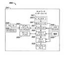
図2乃至図5は、表示用途においてインターフェロメトリックモジュレータのアレイを用いるための一つの典型的なプロセス及びシステムを例示した図である。 図2は、本発明のいくつかの態様を組み入れることができる電子デバイスの一実施形態を示すシステムブロック図である。この典型的実施形態においては、該電子デバイスはプロセッサ21を含んでおり、該プロセッサ21は、ARM、Pentium(登録商標)、Pentium II(登録商標)、Pentium III(登録商標)、Pentium IV(登録商標)、Pentium Pro(登録商標)、8051、MIPS(登録商標)、Power PC(登録商標)、ALPHA(登録商標)、等の、どのような汎用のシングルチップ又はマルチチップのマイクロプロセッサでも、また、デジタル信号プロセッサ、マイクロコントローラ、プログラマブルゲートアレイ、等のどのような専用マイクロプロセッサであっても良い。当該分野において一般的であるように、上記プロセッサ21は、一つ以上のソフトウェアモジュールを実行するように構成することができる。上記プロセッサは、オペレーティングシステムを実行することに加えて、ウェブブラウザ、電話に関するアプリケーション、電子メールプログラム、又はその他のあらゆるソフトウエアアプリケーションを含む、一つ以上のソフトウエアアプリケーションを実行するように構成することができる。FIGS. 2-5 are diagrams illustrating one exemplary process and system for using an array of interferometric modulators in a display application. FIG. 2 is a system block diagram illustrating one embodiment of an electronic device that may incorporate some aspects of the invention. In this exemplary embodiment, the electronic device includes a
一実施形態においては、プロセッサ21は、また、アレイコントローラ22と通信するように構成されている。一実施形態においては、アレイコントローラ22は、画素アレイ30に信号を供給するロードライバ回路24及びコラムドライバ回路26を含む。上記アレイの図1に示した横断面は、図2では線1−1によって示してある。MEMSインターフェロメトリックモジュレータにおいては、ロー/コラム作動プロトコルは、図3に示したこれらのデバイスのヒステリシス特性を利用することができる。例えば、移動可能層を解放状態から作動状態に変形させるためには、10Vの電位差が必要である。しかしながら、電圧をその値から減じたときには、電圧が10Vより低下して戻ったとしても、上記変位可能層はその状態を維持する。図3の例示的な実施形態においては、変位可能層は、電圧が2Vよりも低くなるまで、完全には解放されない。従って、図3に示した例においては約3乃至7Vである、デバイスが解放された状態又は作動された状態で安定している印加電圧のウィンドが存在している電圧範囲がある。本明細書においては、これを「ヒステリシスウィンド」又は「安定ウィンド」と称する。図3に示したヒステリシス特性を有するディスプレイアレイの場合は、ローストローブの間、そのストローブされたロー内の作動対象画素が約10Vの電圧差にさらされ、且つ、解放対象画素が約0Vの電圧差にさらされることになるように、ロー/コラム作動プロトコルを設計することができる。そのストローブ後は、画素は、約5Vの定常状態電圧差にさらされ、このため、上記ローストローブによって置かれたあらゆる状態にとどまる。本例においては、各画素は、書かれた後には、3乃至7Vの「安定ウィンド」内の電位差にさらされる。この特長は、図1に示した画素設計を、作動状態又は先在する解放状態の何れであるかにかかわらず同じ印加電圧状態の下で安定させることになる。インターフェロメトリックモジュレータの各画素は、作動状態又は解放状態の何れであるかにかかわらず、本質的には、固定反射層と変位可能反射層とによって形成されたコンデンサであるため、この安定状態は、電力をほとんど浪費せずにヒステレシスウインド内の電圧で維持することができる。本質的に、印加電位が固定されている場合は、画素内には電流は流れ込まない。 In one embodiment, the
典型的な用途においては、第1のロー内の希望する作動画素の組に従ってコラム電極の組をアサートすることによって表示フレームを作ることができる。次に、ローパルスをロー1電極に加え、アサートされたコラムラインに対応する画素を作動させる。次に、アサートされたコラム電極の組を変更し、第2ロー内の所望の作動画素の組に対応させる。次に、ロー2電極にパルスを加え、アサートされたコラム電極に従ってロー2内の該当画素を作動させる。この際、ロー1の画素は、ロー2のパルスによる影響を受けず、ロー1のパルス中に設定された状態にとどまる。このプロセスを一連のロー全体に関して逐次的に繰り返すことによって表示フレームを生成する。一般的には、これらの表示フレームは、秒当たり所望数のフレーム数で、該プロセスを連続的に繰り返すことによって、リフレッシュされ及び/又は新しい表示データによって更新される。画素アレイのロー電極及びコラム電極を駆動して表示フレームを生成するための多種多様なプロトコルもまた周知であり、これらのプロトコルを本発明と関連させて使用することができる。 In a typical application, a display frame can be created by asserting a set of column electrodes according to the desired set of working pixels in the first row. Next, a low pulse is applied to the low 1 electrode, actuating the pixel corresponding to the asserted column line. The asserted set of column electrodes is then changed to correspond to the desired set of working pixels in the second row. Next, a pulse is applied to the
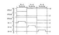
図4及び図5は、図2の3×3のアレイ上において表示フレームを作るための1つの可能な作動プロトコルを例示した図である。図4は、図3のヒステリシス曲線を示している画素に関して使用することができる一組のコラム電圧レベルとロー電圧レベルとを示した図である。図4の実施形態においては、画素を作動させることは、該当するコラムを−Vbiasに設定し且つ該当するローを+ΔVに設定することを含むもので、これらの電圧は、−5V及び+5Vにそれぞれ該当する。画素の解放は、該当するコラムを+Vbiasに設定し且つ該当するローを同じ+ΔVに設定して、該画素において0Vの電位差を作り出すことによって達成される。ロー電圧が0Vに維持されているローにおいては、画素は、コラムが+Vbias又は−Vbiasの何れであるかにかかわらず、最初に置かれていた状態で安定している。4 and 5 are diagrams illustrating one possible operating protocol for creating a display frame on the 3 × 3 array of FIG. FIG. 4 is a diagram illustrating a set of column voltage levels and low voltage levels that can be used for the pixel showing the hysteresis curve of FIG. In the embodiment of FIG. 4, actuating a pixel includes setting the appropriate column to −Vbias and setting the appropriate row to + ΔV, these voltages being −5V and + 5V. Each is applicable. Release of the pixel is accomplished by setting the relevant column to + Vbias and the relevant row to the same + ΔV, creating a 0V potential difference at the pixel. In a row where the row voltage is maintained at 0V, the pixel is stable in its original position regardless of whether the column is + Vbias or -Vbias .
図5Bは、図2の3×3のアレイに印加した一連のロー信号及びコラム信号を示したタイミング図であり、結果的には、図5Aに示した表示配置になる(同図における作動画素は非反射性である)。図5Aに示したフレームを書く前においては、画素はどのような状態であることも可能であり、本例では、すべてのローが0V、すべてのコラムが+5Vとなっている。これらの電圧を印加した状態では、すべての画素は、印加以前における作動状態又は解放状態で安定している。 FIG. 5B is a timing diagram illustrating a series of row and column signals applied to the 3 × 3 array of FIG. 2, resulting in the display arrangement shown in FIG. Is non-reflective). Before writing the frame shown in FIG. 5A, the pixels can be in any state, and in this example, all rows are 0V and all columns are + 5V. In a state where these voltages are applied, all the pixels are stable in an activated state or a released state before the application.
図5Aのフレームにおいては、画素(1、1)、(1、2)、(2、2)、(3、2)及び(3、3)が作動されている。該作動させるためには、ロー1に関する「ラインタイム」の間は、コラム1及び2を−5Vに設定し、コラム3を+5Vに設定する。この場合、すべての画素が3V乃至7Vの安定ウィンド内にとどまっているため、何れの画素の状態も変化しない。次に、ロー1が、0から最高5Vまで上昇させて0に戻るパルスでストローブされる。これは、画素(1、1)及び(1、2)を作動させ、画素(1、3)を解放する。画素アレイ内のその他の画素は影響を受けない。ロー2を希望どおりに設定するためには、コラム2を−5Vに設定し、コラム1及び3を+5Vに設定する。これで、ロー2に加えられた同じストローブが、画素(2、2)を作動させ、画素(2,1)及び(2、3)を解放する。この場合も、画素アレイ内のその他の画素は影響を受けない。同様に、コラム2及び3を−5Vに設定し、コラム1を+5Vに設定することによってロー3は設定される。ロー3のストローブは、ロー3の画素を図5Aに示したように設定する。表示フレームを書いた後は、ロー電位は0であり、コラム電位は、+5V又は−5Vの何れかにとどまることができ、従って、図5Aに示した配置において表示が安定する。この手順は、何十ものローとコラムのアレイさらには何百ものローとコラムのアレイに関しても採用できるという点が高く評価されることになる。さらに、ロー及びコラムの作動を実施するために用いるタイミング、順序、及び電圧レベルは、上述した一般原理内において大きく変化させることが可能である点、及び、上例は典型的な例であるにすぎず、本発明の適用範囲内においてあらゆる作動電圧方法を用いることができる点、も高く評価されることになる。 In the frame of FIG. 5A, the pixels (1, 1), (1, 2), (2, 2), (3, 2) and (3, 3) are activated. To do so, during the “line time” for
上記の原理に従って動作するインターフェロメトリックモジュレータの構造の細部は、大きく変更することができる。例えば、図6A乃至図6Cは、変位式鏡構造物の3つの異なった実施形態を示した図である。図6Aは、図1の実施形態の横断面であり、金属材料14のストリップが、直交する方向に延びている支持物18の上に、蒸着されている。図6Bにおいては、変位可能な反射材料14が、支持物に、その角でのみ、つなぎ材32で取り付けられている。図6Cにおいては、変位可能な反射材料14は、変形可能層34から吊り下げられている。この実施形態においては、反射材料14に関して用いられる構造設計及び材料を光学的性質に関して最適化することができ、さらに、変形可能層34に関して用いられる構造設計及び材料を希望する機械的性質に関して最適化することができるため、いくつかの利点を有している。様々な文献、例えば、米国公開第2004/0051929号、において様々な型のインターフェロメトリックデバイスの生産に関する説明が行われている。材料成膜、パターニング、及びエッチングの一連の手順が関わる上記の構造物は、非常に様々な良く知られた技術を用いて生成することができる。 The details of the structure of interferometric modulators that operate according to the above principles can vary greatly. For example, FIGS. 6A through 6C show three different embodiments of the displacement mirror structure. FIG. 6A is a cross section of the embodiment of FIG. 1, in which a strip of
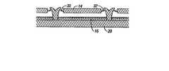
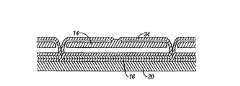
インターフェロメトリックモジュレータアレイのようなMEMSデバイスの変位部分は、変動する保護空間を持つことが好ましい。MEMSデバイスのパッケージング技術が、以下に、より詳細に説明される。インターフェロメトリックモジュレータアレイのようなMEMSデバイスの基本パッケージ構造が、図7に図示されている。図7に示されるように、基本パッケージ構造70は、基板72と、バックプレーンカバー即ち「キャップ」74とを含もので、インターフェロメトリックモジュレータアレイ76はその基板72上に形成される。このキャップ74は、「バックプレート」とも称される。 The displacement portion of a MEMS device, such as an interferometric modulator array, preferably has a fluctuating protective space. MEMS device packaging techniques are described in more detail below. The basic package structure of a MEMS device such as an interferometric modulator array is illustrated in FIG. As shown in FIG. 7, the
インターフェロメトリックモジュレータアレイ76が、基板72、バックプレーン74及びシール78によって封入されるように、基板72とバックプレーン74とがシール78によって接合されて、パッケージ構造70を形成する。これによって、バックプレーン74と基板72との間に空洞79が形成される。上記シール78は、従来のエポキシベースの接着剤のような非機密シールであることができる。他の実施形態においては、上記シール78は、それは、約0.2〜4.7g mm/m2kPa dayの水蒸気の通気性範囲を持つことができる数ある他のタイプのシールの中で、ポリイソブチレン(時にブチルゴムやPIBと称される)、オーリング、ポリウレタン、薄膜金属溶接、液体塗布ガラスか、ハンダ、ポリマ、或いはプラスチックであることができる。さらに他の実施形態では、上記シール78は、気密シールであることができる。
いくつかの実施形態においては、パッケージ構造70は、上記空洞79内の湿気を減らすよう構成された乾燥剤80を含む。当業者であれば、気密シールされたパッケージのために乾燥剤が必ずしも必要なものではないが、パッケージ内に在る湿気を制御することが好ましいということを認識しているはずである。一実施形態においては、乾燥剤80は、インターフェロメトリックモジュレータアレイ76とバックプレーン74との間に配置される。気密シール、非気密シールの何れを持つパッケージであっても、乾燥剤が使用されることができる。気密シールを持ったパッケージにおいては、乾燥剤は一般に、パッケージ内部に在る湿気を制御するために使用される。非気密シールを持ったパッケージでは、乾燥剤は、環境からパッケージ内に移動する湿気を制御するために使用されることができる。一般に、インターフェロメトリックモジュレータアレイの光学特性に干渉することなく湿気を取ることができるものであれば、いかなる物質も乾燥剤80として使用できる。乾燥剤の適当な材料としては、ゼオライト、モレキュラーシーブ、表面吸着剤、バルク吸着剤、化学反応物があるが、それに限定されるものではない。 In some embodiments, the
乾燥剤80は、異なる形態、形状、サイズであることができる。乾燥剤80は、固体形態であっても良いし、粉末形態であっても良い。乾燥剤の粉末は、直接パッケージ内に挿入されることもできるし、用途により接着剤に混ぜ合わせられることもできる。他の実施形態においては、乾燥剤80は、パッケージ内側に適用される前に、シリンダやシートのような異なる形状に形成されることができる。 The desiccant 80 can be in different forms, shapes, and sizes. The desiccant 80 may be in a solid form or a powder form. The desiccant powder can be inserted directly into the package or it can be mixed with the adhesive depending on the application. In other embodiments, the desiccant 80 can be formed into different shapes, such as cylinders and seats, before being applied inside the package.
当業者であれば、乾燥剤80は、異なる手段で適用されることができると理解するだろう。一実施形態では、乾燥剤80は、インターフェロメトリックモジュレータアレイ76の一部として成膜される。別の実施形態では、乾燥剤80は、パッケージ70内側にスプレイや浸漬被覆として適用されている。 One skilled in the art will appreciate that the desiccant 80 can be applied by different means. In one embodiment, desiccant 80 is deposited as part of
基板72は、MEMSデバイスがその上に製造される薄膜を持つことができる半透明又は透明の物質であることができる。そのような透明物質としては、ガラス、プラスチック、透明ポリマを含むが、それに限定されるものではない。インターフェロメトリックモジュレータアレイ76は、メンブレンモジュレータもしくは分離可能型のモジュレータから成っても良い。当業者であれば、バックプレーン74は、ガラス、金属、箔、ポリマ、プラスチック、セラミック、半導体材料(例えば、シリコン)のような、適当な材料で形成されることができることを理解するだろう。 The
パッケージングプロセスは、真空中でも、真空より高く周囲圧力までの間の圧力中でも、あるいは、周囲の圧力より高い圧力中でも、達成されることができる。パッケージングプロセスはまた、シーリングプロセスの間の様々且つ制御された高圧力又は低圧力の環境中で、達成されることができる。完全に乾燥した環境中でインターフェロメトリックモジュレータアレイ76をパッケージングすることが効果的であるが、それは必須のことではない。同様に、パッケージング環境は、不活性ガスの周囲状態にあっても良い。周囲状態でのパッケージングは、当該デバイスが、該デバイスの動作に影響を及ぼすことなく周囲状態を通して搬送されることができるので、より低いコストでの処理及び機器選択における融通性のより大きなポテンシャルを許す。 The packaging process can be accomplished in a vacuum, at a pressure between higher than vacuum and up to ambient pressure, or at a pressure higher than ambient pressure. The packaging process can also be accomplished in various and controlled high or low pressure environments during the sealing process. While it is effective to package the
一般に、パッケージ構造中への水蒸気の透過を最小にし、従ってパッケージ構造70内の環境を制御して、それを気密シールすることは、環境が一定に維持されることを確実にするために、好ましいものである。気密シールプロセスの一例は、米国特許第6,589,625号明細書に開示されている。パッケージ内の湿度が、その湿気からの表面緊張がインターフェロメトリックモジュレータ10における変位可能素子(図示せず)の復元力よりも高くなるレベルを超えてしまうと、変位可能素子は、その表面に永久に張り付いてしまう。湿度レベルが非常に低い場合には、そのコーティングされた表面と変位可能素子が接触した時、湿気は、変位可能素子と同じ極性まで充電する。 In general, it is preferable to minimize the permeation of water vapor into the package structure and thus control the environment within the
上述したように、パッケージ構造70内に在る湿気を制御するために乾燥剤が使用されることができる。しかしながら、パッケージ構造70の内部に雰囲気から湿気が伝わるのを妨げる気密シール78を作成することで、乾燥剤の必要性は減らされる、もしくは無くすことができる。 As described above, a desiccant can be used to control the moisture present in the
表示デバイスの寸法を小さくすることが続けられており、それは、パッケージ構造70内に乾燥剤80を設定する領域をより小さくしていくので、パッケージ構造70内で環境を管理するために入手可能な方法を限定してしまう。乾燥剤の必要性を無くすことは、また、パッケージ構造70を薄くすることを許し、それはいくつかの実施形態では好ましいものである。一般に、乾燥剤を含むパッケージにおいては、そのパッケージされたデバイスの寿命予測は、乾燥剤の寿命に依存すると言ってもさしつかえない。乾燥剤が完全に消費されると、十分な湿気がパッケージ構造に入って、インターフェロメトリックモジュレータアレイに損害を与えるので、該インターフェロメトリックモジュレータデバイスは故障してしまう。いくつかの実施形態においては、MEMS構成部材、この実施形態のためにはインターフェロメトリックモジュレータベースディスプレイ、のパッケージングは、通常は電子回路基板を使用して、ドライバ、プロセッサ、メモリ、その他を含む電子的な構成部材が搭載され且つ相互接続された媒体を提供する。インターフェロメトリックモジュレータマトリックスのバックプレートが、一般的には、当該アレイの機能に干渉することができる、分子及びガスに対する障壁を提供する以外の目的のためには働かないとはいえ、それは、他の機能を持つことができる。その代わりに多層のラミネートバックプレートに頼ることによって、バックプレートは、前述の部品及び構成部材を支持し相互接続する機能と共に、インターフェロメトリックモジュレータを保護するために機能することができる。ラミネートバックプレーンは、また、ドライバ構成部材とディスプレイ間の相互接続としても動作することができる。 Continued to reduce the size of the display device, which will be available to manage the environment within the
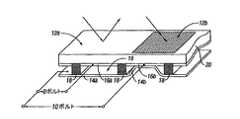
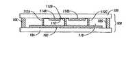
図8は、バックプレート108が様々な電子的な構成部材を支持するよう機能するパッケージ構造100の実施形態を示している。同図に示すように、インターフェロメトリックモジュレータのアレイ102が透明基板104上に設けられる。従って、上記アレイ102は、光を変調して、基板104を通して観察者の方へそれを反射するための手段を提供し、上記基板104は、上記アレイ102を支持するための手段を提供する。シール材106は、上記透明基板104をバックプレート108に接合し、アレイ102のまわりに保護空洞110を形成する。この実施形態においては、インターフェロメトリックモジュレータのアレイ102の範囲内に、バックプレート108を更に支持するポスト112が設けられており、バックプレートが上記アレイ102と接触することを防止している。バックプレート108は、当該バックプレート108の裏面に設けられる、より詳細に後述される種々の電子的構成部材114A,114Bを物理的に支持するものとなる。 FIG. 8 illustrates an embodiment of a
ある実施形態では、あるポスト112A〜112Cは導電性であり、電子的構成部材114A,114Bとアレイ102との間の電気的接続は、上記導電性ポスト112A〜112Cを、上記構成部材114A,114Bと電気的に接続されている、上記バックプレート108上に設けられた導電性トレース116と接触させることによってなされることができる。従って、そのような導電性ポスト及びトレースは、上記電子的構成部材114A,114Bを上記アレイ102と電気的に通信させるための手段を提供する。 In some embodiments,
上記バックプレートが電子的構成部材のために物理的な支持を提供する別の実施形態においては、一例では、上記基板上に配された導電性バンブと上記バックプレート上に配された導電性バンブとに接触をもたらすことによって、上記電子的構成部材と上記アレイの電気的な接続がなされることができる。他の例としては、導電性バンブと上記バックプレート上に設けられた導電性ポストとに接触をもたらすことによって、上記バックプレートと上記インターフェロメトリックアレイの電気的な接続がなされることができる。異方性導電性フィルム(ACF)又は他の導電性材料の層が、これらの電気的接続を作る際に使用されることができ、もしくは、これらの接続は、例えば2つの導電性バンプ間の金属−金属接続であっても良い。そのような別の実施形態は、また、電子的構成部材に上記アレイとの電気的な通信をもたらすための手段を提供する。 In another embodiment in which the backplate provides physical support for electronic components, in one example, a conductive bump disposed on the substrate and a conductive bump disposed on the backplate. By making contact with each other, an electrical connection between the electronic component and the array can be made. As another example, electrical connection between the back plate and the interferometric array can be made by bringing a conductive bump into contact with a conductive post provided on the back plate. A layer of anisotropic conductive film (ACF) or other conductive material can be used in making these electrical connections, or these connections can be, for example, between two conductive bumps A metal-metal connection may be used. Such another embodiment also provides a means for providing an electronic component with electrical communication with the array.
更に別の実施形態では、フレックスケーブル又は同様のコネクタが、バックプレートの表面とインターフェロメトリックモジュレータの表面との間の電気的接続を提供するために使用されることができる。図8の実施形態で記載したように、電子的構成部材がバックプレートの裏面に設けられる必要はないこともまた理解されるだろう。電子的構成部材のいくつか又は全てが、バックプレートの上面上に設けられることができ、電気的な接続は、ビア即ち電気的なフィードスルーを使用してバックプレートを通してなされることができる。 In yet another embodiment, a flex cable or similar connector can be used to provide an electrical connection between the backplate surface and the interferometric modulator surface. It will also be appreciated that electronic components need not be provided on the back side of the backplate, as described in the embodiment of FIG. Some or all of the electronic components can be provided on the top surface of the backplate, and electrical connections can be made through the backplate using vias or electrical feedthroughs.
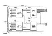
図9は、種々の電子的構成部材が製作されたバックプレート120の裏面を示す図である。ロードライバ回路122及びコラムドライバ回路124がバックプレート120上に配され、該ドライバ回路122,124への及びそれらの間の電気的な接続は、導電性トレース126によって提供されている。上記ドライバ回路122,124は、上記トレース126介して電圧発生器127に電気的に接続されている。上記ドライバ回路122,124はまた、導電性バンプ134を含む、パッド132a及び132bと電気的に通信している。グラフィック処理ユニット(GPU)128が、トレース126を介して上記ドライバ回路122,124と電気的に接続している。更に、低電力回路130が、GPU128と電気的に接続している。 FIG. 9 is a view showing the back surface of the back plate 120 on which various electronic components are manufactured. A
パッド132a,132bは、インターフェロメトリックモジュレータのアレイがその上に提供される透明基板の上面上に設けられた対応するパッドと整列するように構成されている。上記透明基板上の上記対応するパッドは、導電性バンプを持ち、上記対応するパッドが、上記透明基板上のインターフェロメトリックモジュレータのアレイのコラム及びローそれぞれと電気的に接続している。従って、上述した種類のバンプ−バンプ接続は、上記ドライバ回路122,124の出力と上記アレイのロー及びコラムとの間の電気的な接続を提供する。上述したように、上記アレイのローが一つずつ、各コラムに情報を提供するために上記コラムドライバ回路124を使用して一つずつアドレスされ、上記ロードライバ回路122介してアドレスされるべきローをストローブすることができる。従って、上記ドライバ回路のような電子的構成部材は、インターフェロメトリック素子の上記アレイの状態を制御するための手段を提供し、上記バックプレート120は、上記電子回路を支持するための手段を提供する。 The pads 132a, 132b are configured to align with corresponding pads provided on the top surface of the transparent substrate on which the array of interferometric modulators is provided. The corresponding pad on the transparent substrate has conductive bumps, and the corresponding pad is electrically connected to each column and row of the array of interferometric modulators on the transparent substrate. Thus, a bump-bump connection of the type described above provides an electrical connection between the outputs of the
上記電圧発生器は、例えばマキシムMAX1605、MAX686、MAX1955、MAX1561のような市販のユニットや所望の電圧調整を行うことができるいかなる回路であっても構わない。別の好ましい実施形態においては、上記電圧発生器は、使用されている特定の用途のために開発されることができる。上記電圧発生器127は、2つの入力136a,136bを有して提供される。図9の実施形態においては、第1の入力136aが電源電圧(例えば3.3V)であり、第2の入力134bがグラウンドである。上記電圧発生器は、上記電源電圧より大きい又は小さい電位差がロー又はコラムに印加されることができるように、導電性トレース126介して上記ロー及びコラムドライバ122,124に変更された電圧を供給する。従って、上記電圧発生器127は、ステップアップ回路(ブースト回路とも称される)又はステップダウン回路とすることができる。 The voltage generator may be a commercially available unit such as Maxim MAX1605, MAX686, MAX1955, MAX1561, or any circuit capable of performing a desired voltage adjustment. In another preferred embodiment, the voltage generator can be developed for the particular application being used. The
上記GPU128は、例えば、Chips and Technology 69030のような市販のユニットであることができる。別の好ましい実施形態にあっては、上記GPU回路は、使用される特定の用途のために開発されることができる。図9に示された実施形態においては、上記GPU128は、三つの入力138A,138B,138C(それぞれ、クロック、データ及び制御)を受け、特定のロー及びコラムドライバ回路122,124(例えば、TFT、STN、CSTNフォーマット)に必要とされるフォーマットに、データを変換するように構成されている。図9の実施形態では、上記GPUは、上記コラムドライバ124には三つの信号(クロック、データ及び制御)を、また上記ロードライバ122には二つの信号(クロック及び制御)だけを与える。 The
上記低電力回路130は、表示された画像を比較的低電力入力で維持することができる低電力モードに入ることをディスプレイに許すために使用される。例えば、これは、上記GPU128から上記ロー及びコラムドライバ回路122,124へのクロック及びデータ信号を停止することによって行われることができる。上述したように、アレイの中の個々のモジュレータが解放状態又は作動状態の何れかに動かされたならば、上記モジュレータをその位置に維持するのに非常に小さいバイアス電圧で十分であるので、そのような低電力回路130の使用は、インターフェロメトリックモジュレータのアレイを使用するディスプレイに関して特に有益である。さらに、上述のように、このプロセスの間は、ほとんど電力は浪費されない。 The
図9に示された電気的構成部材は例示的なものであることは、理解されるだろう。他の実施形態は、より多くの又はより少ない電気的構成部材を含んでも良いし、多数の機能が一つの構成部材によって得られるものであっても良い。更に、上記パッケージが組立てられた際に、それらが上記シール材によって形成された上記保護空洞内に配されるように、図9の上記構成部材が上記バックプレートの裏面上に全てあるかのように記載されているが、上記構成部材が上記保護空洞の外側にあるように、上記構成部材のうちの一部が、上記バックプレート上や、上記シール材を越えて延在する上記透明基板の張り出し部上のような、どこかほかに配しても構わない。 It will be understood that the electrical components shown in FIG. 9 are exemplary. Other embodiments may include more or fewer electrical components, and multiple functions may be provided by a single component. Furthermore, it is as if the components in FIG. 9 are all on the back surface of the back plate so that, when the packages are assembled, they are arranged in the protective cavity formed by the sealing material. However, a part of the constituent members of the transparent substrate extends on the back plate or beyond the sealing material so that the constituent members are outside the protective cavity. It may be placed somewhere else, such as on the overhang.
上記パッケージの外部と上記パッケージの内部との間の電気的な接続は、種々の手法で行われることができる。例えば、バックプレーンがガラス、あるいは、予め製作された何か他の材料の層であるとき、上記電気的な接続は、導電性トレースが上記シールの下を通過するように上記バックプレートの表面に沿って走っている導電性トレースを備えることができる。上記バックプレートがバックプレートとして使用されるために製作されるとき、上記バックプレートは、好ましくは、上記バックプレートの上面と下面の間の電気的な接続を提供する電気的なビア、即ちフィードスルーを含むように製作されても良い。そのようなビアは、更に、ガラスあるいは他の予め製作したバックプレート材料を通して提供されても良いが、そのようなビアの追加は、より難しく、時間がかかり、高価となるだろう。 The electrical connection between the outside of the package and the inside of the package can be made in various ways. For example, when the backplane is glass or a layer of some other prefabricated material, the electrical connection is made to the surface of the backplate so that the conductive traces pass under the seal. Conductive traces running along can be provided. When the back plate is fabricated for use as a back plate, the back plate preferably has electrical vias or feedthroughs that provide an electrical connection between the top and bottom surfaces of the back plate. It may be manufactured to include. Such vias may also be provided through glass or other prefabricated backplate materials, but adding such vias will be more difficult, time consuming and expensive.
更に別の実施形態においては、上記電子回路は、上記バックプレートとして機能する基板上に薄膜層を成膜し、特定用途向け集積回路(ASIC)を製作することによって形成されることができる。図10の断面図に、そのようなASIC140の例が示されている。上記ASIC140は、例えばガラス層である薄膜成膜ASIC台142上に、複数の層を成膜することによって形成される。上記台142は、上述したそれらと同様のディスプレイパッケージのためのバックプレートとして機能するガラス層から成っていても良い。ASIC台140として、どのような適当な材料を使用しても構わない。 In yet another embodiment, the electronic circuit can be formed by depositing a thin film layer on a substrate that functions as the backplate to produce an application specific integrated circuit (ASIC). An example of such an
そして、非結晶シリコンが、上記ASIC台142上に成膜される。図10の実施形態においては、非結晶p型シリコン層144が上記台142上に成膜され、ウェルとも称される領域145a,145bにn型非結晶シリコンが埋め込まれる。そのようなウェル145a,145bは、特定のトランジスタのドレイン又はソースとなるだろう。上記ASIC140においては、上記ウェル145aはトランジスタのソースとして機能し、上記ウェル145bはドレインとして機能する。例えば、上記シリコンは、フォトリソグラフィ法によって、または当業者に知られている他の適当な技術によって、成膜されることができる。上記層144の基材と上記ウェル145a,145bとの間のpn接合は、急速熱アニーリング(RTA)のような又はレーザの使用を通しての技術を使用して形成されることができる。図10にはp型トランジスタが示されているが、層144のn型シリコンを成膜し、上記ウェル145a,145bのp型シリコンを埋め込むことによって、n型トランジスタが作製されることができることは、理解されるだろう。 Then, amorphous silicon is deposited on the
その後、図10の上記ASIC140ではSi02の層であるが、いかなる適当な絶縁層も使用されることができる絶縁層146で、上記ドープドシリコン層144が覆われる。上記成膜は、例えば化学蒸着法(CVD)や他のどの適当な方法によってもなされることができる。例えばモリブデンであることができる導電性材料150が、上記ウェル145a,145bの間の上記絶縁層146の上面に成膜されて、トランジスタのゲートを形成する。上記導電性材料150を成膜するためには、エッチングプロセスを使用しても良い。この実施形態ではシリコン硝酸塩のような硝酸塩であることができる追加の絶縁材料層148が、上記導電性材料150と上記絶縁層146の上に成膜される。 Thereafter, the doped
上記絶縁層148,146を通る導電性経路がエッチングされ、上記ゲート150及び埋め込み領域145a,145bを露出する。金属152が成膜されて上記ゲート150、上記ソース145a及び上記ドレイン145bへの接続が形成され、それによってトランジスタが形成される。この金属層の成膜は、適当な位置に形成するよう上記金属152をエッチングするためのマスクを使用して行われることができる。層152の上に、追加の金属層153が形成され、一連の平行ライン(図示せず)を備えることができる。一般的には、一連の平行ラインとしてのそれらの構成のために、層153のようなASICで使用される金属層は、一方向にだけ延在する。複数トランジスタ間の接続は、層153を形成するために金属を所望のパターンでフォトグラフ法で成膜することによって形成される。従って、層153は、所望のパターンでトランジスタを接続することによって論理的な機能を形成する。 Conductive paths through the insulating
層153の上に、金属層154が形成される。図10に見られることができるように、層154は、ページに直交する、従って層153の上記平行ラインに垂直な向きにされた一連の平行ラインを備える。層154は、該ASIC140に電力を提供するために使用される。層154の上には、別の金属相互接続層155が形成され、より複雑な論理接続を完成する。相互接続層155の上には、グラウンド層156が形成される。層154〜156のそれぞれは、平行ラインを備えることができ、フォトリソグラフィ法によりパターニングされることができる。例えば上記金属層に穴を開けて金属をその穴に堆積することによって形成されることができるビアを通して、上記金属層の間の相互接続が提供されることができる。更に、一実施形態では、上記層153〜156が平行ラインを備えるとはいえ、他の実施形態では、これらは平行ラインを作らない層を成膜することによって形成されるようにしても良い。従って、上記金属層を成膜するかエッチングすることによって及び上記層間の相互接続を形成することによって、トランジスタ間の所望の相互接続が作製されることができる。 A
層156上の上面金属層157は、外部相互接続層として機能するもので、該ASICの論理ゲートと入力/出力との間の接続を提供する。図10の実施形態においては、上記上面金属層157は、一連の平行ラインで形成されるものではなく、従って多数の方向に延在し、より複雑な相互接続を可能にする。上記上面金属層をエッチングするために、当業者に知られたいかなる適当な方法でも良いマスキング及びフォトリソグラフィ技術が使用されることができる。ASIC140が上述したようなディスプレイパッケージ中の電子回路を形成する実施形態においては、この用途で説明されたどの方法でも、あるいは他のどの適当な方法でも使用して、上記金属外部結合層148は、上記ASIC140とインターフェロメトリックモジュレータの上記アレイ(図示せず)との間の接続を提供する。 A
種々の実施形態において、上記成膜台144はガラスから成る必要はなく、むしろ、成膜された薄膜回路を載せるのに適当ないかなる材料から成っても良い。図9に関して上述したように、上記成膜台144は、ディスプレイパッケージの内部とディスプレイパッケージの外部との間に電気的な接続を可能にする様々な特長の何れを含んでも良い。これらの特長は、それに限定するものではないが、電気的なフィードスルー即ちビア、及び、上記成膜台144内部の電気的な相互接続を含むことができる。 In various embodiments, the
電子回路の製作は、インターフェロメトリックベースのディスプレイパッケージの製造において多くの効果を提供することができる。製作を通して可能にされる回路のカスタム化は、空間の効率的利用を許す。LCDのような他ディスプレイデバイスと違って、インターフェロメトリックモジュレータベースのディスプレイは、画素アレイの上に直接配され且つ上記基板と上記バックプレートによって形成された「サンドイッチ」内に配される電子回路の包含を許す。その程度の必要とされた電子回路を、上記基板の上記保護空洞外部の張り出し部上よりはむしろ、その位置に配置することによって、上記ディスプレイの設置面積が最小にされることができる。更に、上記ドライバ回路とインターフェロメトリックモジュレータのアレイとの間の接続は、複雑であり得、一つの出力と上記アレイの各ロー及びコラムの接続と同程度を必要とする。上記ドライバ回路を製作することによって、これらの出力の配置及びこれらの出力と上記アレイとの間の相互接続に対するより大きな制御量が得られる。更に、ドライバ回路や他の電子回路の積層は、予め製作された電子回路から成るディスプレイパッケージよりも、薄く且つ安価なディスプレイパッケージの作成を可能にすることができる。 Electronic circuit fabrication can provide many benefits in the manufacture of interferometric based display packages. Circuit customization made possible through fabrication allows for efficient use of space. Unlike other display devices such as LCDs, interferometric modulator-based displays consist of electronic circuitry that is placed directly on the pixel array and in a “sandwich” formed by the substrate and the backplate. Allow inclusion. By placing such required electronic circuitry at that location rather than on the overhanging portion of the substrate outside the protective cavity, the display footprint can be minimized. Furthermore, the connection between the driver circuit and the array of interferometric modulators can be complex, requiring as much as one output and the connection of each row and column of the array. By producing the driver circuit, a greater amount of control over the placement of these outputs and the interconnection between these outputs and the array is obtained. Furthermore, the stacking of driver circuits and other electronic circuits can make it possible to create a display package that is thinner and less expensive than a display package made of prefabricated electronic circuits.
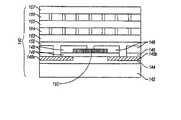
図11は、ドライバ回路のような電子回路162が薄膜成膜によってバックプレート164の裏面に製作されたパッケージ160の実施形態を示している。金属バンプ166A〜166Cは、金属スペーサ即ち支持ポスト168A〜168Cに合わせられて、上記電子回路162と基板172上に設けられたインターフェロメトリックモジュレータのアレイ170との間に電気的な接続を提供する。従って、上記バンプ166A〜166C及びポスト168A〜168Cは、上記回路162と上記アレイ170とを電気的に接続するための手段を提供する。 FIG. 11 shows an embodiment of a
基板172及びバックプレート164と共に、シール材174は、上記アレイ170の周囲に保護空洞176を形成する。上記パッケージの外部と上記電子回路162との間の電気的な接続は、上記バックプレート164の裏面に沿って且つ上記シール材174を超えて走る導電性トレース178によってなされる。上記電子アレイの動作のために必要とされる導電性トレース178の数は、上記バックプレート164の裏面に製作された電子回路162の種類に依存する。上記電子回路162がドライバ回路を含むときには、上記パッケージ160の内部と外部との間に延在するトレース178の必要数は、非常に減じられることができる。同様に、上記バックプレートの裏面にGPU回路、ブースト回路や低電力回路を製作すれば、パッケージ160の内部と外部との間に必要とされる相互接続を単純化することができる。 Together with the
図11に示されたパッケージ160は、製作された電子回路162を含むが、別の実施形態においては、上記電子回路が、マイクロチップから成ったり、当該製作された電子回路と共に集積化された他の予め製作された回路とから成ったりすることができることは理解されるだろう。例えば、ドライバ回路とブースト回路が、上記バックプレートの裏面に製作され、市販のGPU及び低電力回路に接続されても良い。 The
図12A及び図12Bは、熱圧縮によるパッケージ180の組立てを示す図である。図12Aは、熱圧縮前のパッケージ180の断面図であり、図12Bは、熱圧縮後のパッケージ180の断面図である。 12A and 12B are diagrams showing assembly of the
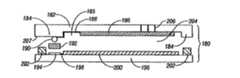
図12Aに関しては、窪み領域185がより厚い足部184に囲まれているように、バックプレート182が異なっている厚みを持つことが、見られることができる。電子回路186は、上記窪み領域185内に構成され、ビア206を通して上記バックプレート182の上面と電気的に通信している。上記電子回路186は、また、上記ビア206の裏面に沿って走って上記足部184の少なくとも下面207に延びている導電性トレース188と電気的に通信している。上記導電性トレース188と透明基板196の上面に配されたパッド194との間に、金導電性物質190とACF層192とが配置されている。上記パッド194は、また、インターフェロメトリックモジュレータのアレイ200と電気的な通信を提供する、トレース、バンプ或いは他のコネクタであることができることは、理解するべきである。上記パッド194は、導電性トレース198により、上記透明基板196の上面に配されたインターフェロメトリックモジュレータのアレイ200と電気的に通信している。シール材202は、上記バックプレート182を上記基板196に接合して、上記アレイ200の周囲に保護空洞204を形成する。 With respect to FIG. 12A, it can be seen that the
次に、熱圧縮の後、よりコンパクトな形状となった上記パッケージ180を示す図12Bに関して、金導電性物質190とACF192とが圧縮されて、上記電子回路186と上記アレイ200との間に電気的な接続を提供し、それによって、上記アレイ200における反射素子の状態を制御することを上記電子回路186に可能にさせる、ということが見られることができる。従って、上記回路186を上記アレイ200と通信している状態にするための手段が提供される。上記電子回路184が製作された上記バックプレート182の上記窪み領域185は、隙間を有して上記電子回路を提供し、上記熱圧縮プロセスの間の損傷から上記回路を保護するということが見られることができる。 Next, with reference to FIG. 12B, which shows the
図13A及び図13Bは、ディスプレイデバイス2040の一実施形態を示すシステムブロック図である。上記ディスプレイデバイス2040は、例えば携帯電話機や移動式電話機であることができる。しかしながら、それについて、ディスプレイデバイス2040と同じ構成部材やその僅かな変形例は、テレビ受像機及びポータブルメディアプレイヤのようなディスプレイデバイスの種々の種類の実例ともなる。 13A and 13B are system block diagrams illustrating one embodiment of a
上記ディスプレイデバイス2040は、ハウジング2041、ディスプレイ2030、アンテナ2043、スピーカ2045、入力デバイス2048及びマイクロフォン2046を含む。上記ハウジング2041は、一般的に、射出形成法及び真空成形を含む当業者の間でよく知られているような様々なあらゆる製造プロセスにて形成される。更に、上記ハウジング2041は、それに限定されるものではないが、プラスチック、金属、ガラス、ゴム及びセラミック、またはそれらの組み合わせを含む様々なあらゆる材料から製作されることができる。一実施形態においては、上記ハウジング2041は、異なる色、異なるロゴ、絵またはシンボルを含む他の除去可能な部分と交換できる除去可能な部分(図示せず)を含む。 The
本明細書に記載されるように、例示的なディスプレイデバイス2040の上記ディスプレイ2030は、双安定ディスプレイを含む様々なディスプレイの何れであっても良い。他の実施形態においては、上記ディスプレイ2030は、上述したようなプラズマ、EL、OLED、STN LCD、TFT LCDのようなフラットパネルディスプレイや、当業者によく知られているようなCRTや他のチューブデバイスのような非フラットパネルディスプレイを含む。しかしながら、本実施形態を説明するという目的に照らすと、上記ディスプレイ2030は、本明細書に記載されたようなインターフェロメトリックモジュレータディスプレイを含む。 As described herein, the
例示的なディスプレイデバイス2040の一実施形態の構成部材は、図13Bに概略的に示されている。図示された例示的なディスプレイデバイス2040は、ハウジング2041を含み、少なくとも部分的にその中に封入された追加の構成部材を含むことができる。例えば、一実施形態では、上記例示的なディスプレイデバイス2040は、トランシーバ2047に連結されたアンテナ2043を含むネットワークインターフェース2027を含む。上記トランシーバ2047は、コンディショニングハードウェア2052に接続されているプロセッサ2021に接続されている。上記コンディショニングハードウェア2052は、信号を調整する(例えば、信号をフィルタリングする)ように構成されている。上記コンディショニングハードウェア2052は、スピーカ2045及びマイクロフォン2046に接続されている。上記プロセッサ2021は、また、入力デバイス2048及びドライバコントローラ2029に接続されている。上記ドライバコントローラ2029には、フレームバッファ2028が接続されていると共に、ディスプレイアレイ2030に更に接続されたアレイドライバ2022が接続されている。電源2050は、特定の例示的なディスプレイデバイス2040の設計によって必要とされるような全ての構成部材に電力を供給する。 The components of one embodiment of
上記例示的なディスプレイデバイス2040がネットワーク上の一つ以上のデバイスと通信することができるように、上記ネットワークインターフェース2027は上記アンテナ2043及び上記トランシーバ2047を含む。一実施形態においては、上記ネットワークインターフェース2027は、また、若干の処理能力を持ち、上記プロセッサ2021の要求を軽減するようにしても良い。上記アンテナ2043は、信号の送受信に用いられる当業者によく知られて何れかのアンテナである。一実施形態では、上記アンテナは、IEEE802.11(a),(b)又は(g)を含むIEEE802.11規格に従ってRF信号の送受信を行う。他の実施形態においては、上記アンテナは、BLUETOOTH(登録商標)規格に従ってRF信号を送受信する。携帯電話機の場合、上記アンテナは、CDMA、GSM、AMPSまたは既知の信号がワイヤレス携帯電話機ネットワーク内で通信を行うために使用される他の既知信号を受信するよう設計されている。上記トランシーバ2047は、該トランシーバ2047によって受信され上記プロセッサ2021によって更に処理されることができるように、上記アンテナ2043から受信された信号を前処理する。上記トランシーバ2047はまた、それらが該例示的なディスプレイデバイス2040から上記アンテナ2043介して送信されることができるように、上記プロセッサ2021から受けた信号を処理する。 The
別の実施形態では、上記トランシーバ2047は、受信機と置き換えることができる。さらに別の実施形態では、ネットワークインターフェース2027は、上記プロセッサ2021に送られるべきイメージデータを格納或いは生成することができるイメージソースに置き換えられることができる。例えば、上記イメージソースは、イメージデータを含むデジタルビデオディスク(DVD)やハードディスクドライブ、またはイメージデータを生成するソフトウェアモジュールであることができる。 In another embodiment, the
プロセッサ2021は、一般に、上記例示的なディスプレイデバイス2040の全動作を制御する。上記プロセッサ2021は、上記ネットワークインターフェース2027やイメージソースからの圧縮したイメージデータのようなデータを受信し、RAWイメージデータに、またはRAWイメージデータに容易に処理されるフォーマットに、その受信したデータを処理する。その後、上記プロセッサ2021は、上記ドライバコントローラ2029に、または記憶するためにフレームバッファ2028に、上記処理されたデータを送る。RAWデータとは、一般的には、イメージ内の各位置でのイメージ特徴を識別する情報を指す。例えば、そのようなイメージ特徴は、色、彩度及び階調レベルを含むことができる。 The
一実施形態においては、上記プロセッサ2021は、マイクロコントローラ、CPU、又は論理ユニットを含み、上記例示的なディスプレイデバイス2040の動作を制御する。コンディショニングハードウェア2052は、一般的には、上記スピーカ2045に信号を送信するため及び上記マイクロフォン2046から信号を受信するために、増幅器及びフィルタを含む。コンディショニングハードウェア2052は、上記例示的なディスプレイデバイス2040内に別個の構成部材であっても良いし、上記プロセッサ2021や他の構成部材内に組み込まれていても良い。 In one embodiment, the
上記ドライバコントローラ2029は、上記プロセッサ2021から直接または上記フレームバッファ2028から、上記プロセッサ2021によって生成された上記RAWイメージデータを取得し、そのRAWイメージデータを上記アレイドライバ2022へ高速に送信できるように適切に再フォーマットする。特に、上記ドライバコントローラ2029は、上記ディスプレイアレイ2030をスキャンするのに適したタイムオーダを持つようなラスタ状フォーマットを有するデータフローに、上記RAWイメージデータを再フォーマットする。そして、上記ドライバコントローラ2029は、上記アレイドライバ2022にそのフォーマットされた情報を送る。LCDコントローラのようなドライバコントローラ2029は、多くの場合、独立型集積回路(IC)として上記システムプロセッサ2021と関連させられるが、そのようなコントローラは多数の手法で実現されることができる。それらは、ハードウェアとして上記プロセッサ2021に組み込まれても良いし、ソフトウェアとして上記プロセッサ2021に組み込まれても良いし、ハードウェアで上記アレイドライバ2022に完全に集積化されても良い。 The
一般的には、上記アレイドライバ2022は、上記ドライバコントローラ2029から上記フォーマットされた情報を受信し、ディスプレイのx−yマトリックスの画素から来る数百及び時には数千ものリードに、一秒間に多数回印加される並列な波形の組へ、上記ビデオデータを再フォーマットする。 In general, the
一実施形態においては、上記ドライバコントローラ2029、アレイドライバ2022及びディスプレイアレイ2030は、本明細書において記載された何れの種類のディスプレイのためにも適切なものである。例えば、一実施形態では、ドライバコントローラ2029は、従来のディスプレイコントローラや双安定ディスプレイコントローラ(例えば、インターフェロメトリックモジュレータコントローラ)である。他の実施形態においては、アレイドライバ2022は、従来のドライバや双安定ディスプレイドライバ(例えば、インターフェロメトリックモジュレータディスプレイ)である。一実施形態では、ドライバコントローラ2029は、上記アレイドライバ2022と集積化される。そのような実施形態は、携帯電話機、腕時計及び他の小領域ディスプレイのような非常に集積化されたシステムにおいて共通である。さらに別の実施形態においては、ディスプレイアレイ2030は、典型的なディスプレイアレイや双安定ディスプレイアレイ(例えば、インターフェロメトリックモジュレータのアレイを含むディスプレイ)である。 In one embodiment, the
上記入力デバイス2048は、ユーザが上記例示的なディスプレイデバイス2040の動作を制御すること可能にする。一実施形態では、入力デバイス2048は、QWERTYキーボードや電話キーパッドのようなキーパッド、ボタン、スイッチ、タッチ感知スクリーン、圧力感知メンブレン、又は熱感知メンブレンを含む。一実施形態においては、上記マイクロフォン2046は、上記例示的なディスプレイデバイス2040のための入力デバイスである。上記マイクロフォン2046が上記デバイスへのデータ入力に使用される場合には、上記例示的なディスプレイデバイス2040の制御動作のために音声コマンドがユーザによって提供されることができる。 The
電源2050は、当業者に良く知られているように、様々なエネルギー蓄積装置を含むことができる。例えば、一実施形態においては、電源2050は、ニッケルカドミウム電池やリチウムイオンバッテリのような再充電可能なバッテリである。他の実施形態では、電源2050は、回復可能なエネルギソース、コンデンサ、またはプラスチック太陽電池や太陽電池塗料を含む太陽電池である。他の実施形態においては、電源2050は、壁面コンセントから電力を受けるよう構成される。 The
いくつかの実施においては、上記電子ディスプレイシステム中のいくつかの場所に配されることができるドライバコントローラには、上述したように、制御プログラム化可能性がある。いくつかの場合、制御プログラム化可能性は、上記アレイドライバ2022にある。当業者は、上述した最適化は、あらゆるハードウェア及び/又はソフトウェア構成部材の種々の構成において、実現されることができると認めるだろう。 In some implementations, driver controllers that can be placed in several locations in the electronic display system may be control-programmed, as described above. In some cases, the control programmability is in the
以上の詳細な説明は、種々の実施形態に適用されたような本発明の新規な特長を示し、説明し、指摘したが、図示された上記デバイス又はプロセスの形状及び細部の種々の省略、置換及び変更は、本発明の精神から逸脱することなく当業者によってなされることができることは、理解されるだろう。認められるだろうように、本発明は、いくつかの特長が使用される又は他とは別個に実践されることができるように、本明細書に示された上記特長及び利益の全てを必ずしも提供しない形態で具体化されることができる。 Although the foregoing detailed description has shown, described, and pointed out novel features of the present invention as applied to various embodiments, various omissions and substitutions of the shapes and details of the devices or processes illustrated are shown. It will be understood that changes and modifications can be made by those skilled in the art without departing from the spirit of the invention. As will be appreciated, the invention does not necessarily provide all of the features and benefits shown herein so that some features may be used or practiced separately from others. It can be embodied in a form that does not.
Claims (36)
Translated fromJapanese前記透明基板を通して光を反射するよう構成されたる反射素子を含むインターフェロメトリックモジュレータのアレイと、
上記インターフェロメトリックモジュレータのアレイに隣接する第1の面を含み、該第1の面上に、上記反射素子の変位を制御するよう構成された電子回路が製作された、バックプレーンと、
上記バックプレーン上の上記電子回路と上記インターフェロメトリックモジュレータのアレイとの間に電子通信を提供する複数の電気的接続と、
を具備するディスプレイ。A transparent substrate;
An array of interferometric modulators including reflective elements configured to reflect light through the transparent substrate;
A backplane comprising a first surface adjacent to the array of interferometric modulators on which an electronic circuit configured to control displacement of the reflective element is fabricated;
A plurality of electrical connections providing electronic communication between the electronic circuitry on the backplane and the array of interferometric modulators;
A display comprising:
前記プロセッサと電気的に通信しているメモリデバイスと、
を更に具備する請求項1のディスプレイ。A processor in electrical communication with the array of interferometric modulators and configured to process image data;
A memory device in electrical communication with the processor;
The display of claim 1, further comprising:
第1の面を有するバックプレートを提供することと、
上記バックプレートの上記第1の面上に、前記反射素子の状態を制御するよう構成された電子回路を形成することと、
上記透明基板の上記第1の面が上記バックプレートの第1の面に隣接して配置され、且つ、上記電子回路が上記インターフェロメトリックモジュレータのアレイと電気的に接続した状態となるように、上記透明基板と上記バックプレートとを配置することと、
を含む電子ディスプレイを製作する方法。Providing a transparent substrate comprising an array of interferometric modulators comprising a reflective element on its first surface;
Providing a backplate having a first surface;
Forming an electronic circuit on the first surface of the back plate configured to control a state of the reflective element;
The first surface of the transparent substrate is disposed adjacent to the first surface of the back plate, and the electronic circuit is in electrical connection with the array of interferometric modulators. Disposing the transparent substrate and the back plate;
A method of making an electronic display including:
前記透明基板及び前記バックプレートを一緒に熱圧縮し、それによって、上記バンプを平坦にすることと、
を更に含む請求項20の方法。Arranging the transparent substrate and the back plate so that the bumps of the conductive material are in contact with each other;
Thermally compressing the transparent substrate and the back plate together, thereby flattening the bumps;
21. The method of claim 20, further comprising:
前記第1及び第2の導電性材料の両方ともが、上記異方性導電性フィルムの層と電気的に接触しているように、前記透明基板及び前記バックプレートを配置することと、
前記透明基板及び前記バックプレートを一緒に熱圧縮することと、
を更に含む請求項20の方法。Depositing a layer of anisotropic conductive film in contact with either the first or second conductive material;
Disposing the transparent substrate and the back plate such that both the first and second conductive materials are in electrical contact with the layer of the anisotropic conductive film;
Thermally compressing the transparent substrate and the back plate together;
21. The method of claim 20, further comprising:
シリコンベース層を前記バックプレートの第1の面上に成膜することと、
複数の金属層を前記シリコンベース層上に成膜することと、
を含む請求項17の方法。Forming an electronic circuit on the first surface of the backplate,
Depositing a silicon base layer on the first surface of the backplate;
Depositing a plurality of metal layers on the silicon base layer;
The method of claim 17 comprising:
上記バックプレートの第1の面上に複数のトランジスタを形成することと、
上記トランジスタ間に金属による相互接続を形成することと、
を含む請求項17の方法。Forming an electronic circuit on the first surface of the backplate,
Forming a plurality of transistors on the first surface of the backplate;
Forming a metal interconnect between the transistors;
The method of claim 17 comprising:
上記複数のトランジスタと外部の電子回路との間に金属による接続を形成することと、
上記複数のトランジスタと上記インターフェロメトリックモジュレータのアレイとの間に金属による接続を形成することと、
を更に含む請求項25の方法。Forming an electronic circuit on the first surface of the backplate,
Forming a metal connection between the plurality of transistors and an external electronic circuit;
Forming a metal connection between the plurality of transistors and the array of interferometric modulators;
26. The method of claim 25, further comprising:
ドープド非結晶シリコン層を上記透明基板上に成膜することと、
上記ドープド非結晶シリコン層内に反対極性のドープドシリコンを埋め込んで、ウェルを形成することと、
上記非結晶シリコン層及び上記ウェルの上に、第1の絶縁材料層を成膜することと、
上記第1の絶縁材料層の上に、導電性材料から成るゲートを成膜することと、
を含む請求項25の方法。Forming a plurality of transistors on the first surface of the backplate includes
Forming a doped amorphous silicon layer on the transparent substrate;
Embedding doped silicon of opposite polarity in the doped amorphous silicon layer to form a well;
Forming a first insulating material layer on the amorphous silicon layer and the well;
Forming a gate made of a conductive material on the first insulating material layer;
26. The method of claim 25, comprising:
上記ゲート及び上記第1の絶縁材料層の上に、第2の絶縁材料層を成膜することと、
上記第1及び第2の絶縁材料層をエッチングして、上記絶縁材料層を通して上記ウェル及びゲートへの導電性経路を形成することと、
上記第2の絶縁材料層の上に、上記導電性経路を通して延在する第1の金属の相互接続層を成膜することと、
を更に含む請求項27の方法。Forming a plurality of transistors on the first surface of the backplate includes
Depositing a second insulating material layer on the gate and the first insulating material layer;
Etching the first and second insulating material layers to form conductive paths through the insulating material layer to the well and gate;
Depositing on the second insulating material layer a first metal interconnect layer extending through the conductive path;
28. The method of claim 27, further comprising:
上記第1の金属の相互接続層の上に、上面金属層を成膜することと、
上記上面金属層にフォトリソグラフィエッチングを行って、上記接続を形成することと、
を含む請求項28の方法。Forming a metal connection between the plurality of transistors and an external circuit, and forming a metal connection between the plurality of transistors and the external circuit;
Depositing a top metal layer on the first metal interconnect layer;
Performing photolithography etching on the top metal layer to form the connection;
30. The method of claim 28, comprising:
上記送信手段を通して送信された光を変調するための変調手段と、
上記変調手段に隣接する第1の面と、前記第1の面上に製作された上記変調手段の変位を制御するための電子手段とを含む、前記変調手段を覆うためのカバーリング手段と、上記電子手段と上記変調手段との間に電子通信を提供するための提供手段と、
を具備する電子ディスプレイ。A transmission means for transmitting light therethrough,
Modulation means for modulating light transmitted through the transmission means;
Covering means for covering the modulation means, comprising: a first surface adjacent to the modulation means; and electronic means for controlling the displacement of the modulation means fabricated on the first surface; Providing means for providing electronic communication between the electronic means and the modulating means;
An electronic display comprising:
Applications Claiming Priority (2)
| Application Number | Priority Date | Filing Date | Title |
|---|---|---|---|
| US61397704P | 2004-09-27 | 2004-09-27 | |
| US11/090,491US7668415B2 (en) | 2004-09-27 | 2005-03-25 | Method and device for providing electronic circuitry on a backplate |
Related Parent Applications (1)
| Application Number | Title | Priority Date | Filing Date |
|---|---|---|---|
| JP2005258288ADivisionJP2006099101A (en) | 2004-09-27 | 2005-09-06 | Method and device for providing electronic circuitry on backplate |
Publications (1)
| Publication Number | Publication Date |
|---|---|
| JP2010191440Atrue JP2010191440A (en) | 2010-09-02 |
Family
ID=35958971
Family Applications (3)
| Application Number | Title | Priority Date | Filing Date |
|---|---|---|---|
| JP2005258288APendingJP2006099101A (en) | 2004-09-27 | 2005-09-06 | Method and device for providing electronic circuitry on backplate |
| JP2010053564AWithdrawnJP2010191440A (en) | 2004-09-27 | 2010-03-10 | Method and device for providing electronic circuitry on backplate |
| JP2011127159APendingJP2011221548A (en) | 2004-09-27 | 2011-06-07 | Method and apparatus for providing electronic circuit on back plate |
Family Applications Before (1)
| Application Number | Title | Priority Date | Filing Date |
|---|---|---|---|
| JP2005258288APendingJP2006099101A (en) | 2004-09-27 | 2005-09-06 | Method and device for providing electronic circuitry on backplate |
Family Applications After (1)
| Application Number | Title | Priority Date | Filing Date |
|---|---|---|---|
| JP2011127159APendingJP2011221548A (en) | 2004-09-27 | 2011-06-07 | Method and apparatus for providing electronic circuit on back plate |
Country Status (11)
| Country | Link |
|---|---|
| US (4) | US7668415B2 (en) |
| EP (1) | EP1655720A3 (en) |
| JP (3) | JP2006099101A (en) |
| KR (1) | KR101237888B1 (en) |
| AU (1) | AU2005204240A1 (en) |
| BR (1) | BRPI0503855A (en) |
| CA (1) | CA2518396A1 (en) |
| MX (1) | MXPA05010090A (en) |
| RU (1) | RU2005129919A (en) |
| SG (2) | SG155976A1 (en) |
| TW (1) | TW200626950A (en) |
Cited By (1)
| Publication number | Priority date | Publication date | Assignee | Title |
|---|---|---|---|---|
| JP2013538010A (en)* | 2010-09-23 | 2013-10-07 | クゥアルコム・メムス・テクノロジーズ・インコーポレイテッド | Integrated passive elements and power amplifiers |
Families Citing this family (29)
| Publication number | Priority date | Publication date | Assignee | Title |
|---|---|---|---|---|
| JP4342174B2 (en)* | 2002-12-27 | 2009-10-14 | 新光電気工業株式会社 | Electronic device and manufacturing method thereof |
| TWI251712B (en)* | 2003-08-15 | 2006-03-21 | Prime View Int Corp Ltd | Interference display plate |
| TW593127B (en)* | 2003-08-18 | 2004-06-21 | Prime View Int Co Ltd | Interference display plate and manufacturing method thereof |
| US7405924B2 (en)* | 2004-09-27 | 2008-07-29 | Idc, Llc | System and method for protecting microelectromechanical systems array using structurally reinforced back-plate |
| US7675669B2 (en)* | 2004-09-27 | 2010-03-09 | Qualcomm Mems Technologies, Inc. | Method and system for driving interferometric modulators |
| US7668415B2 (en) | 2004-09-27 | 2010-02-23 | Qualcomm Mems Technologies, Inc. | Method and device for providing electronic circuitry on a backplate |
| US7999994B2 (en) | 2005-02-23 | 2011-08-16 | Pixtronix, Inc. | Display apparatus and methods for manufacture thereof |
| WO2007120887A2 (en)* | 2006-04-13 | 2007-10-25 | Qualcomm Mems Technologies, Inc | Packaging a mems device using a frame |
| JP4903540B2 (en)* | 2006-11-29 | 2012-03-28 | 京セラ株式会社 | Substrate for encapsulating microelectromechanical components, substrate for encapsulating microelectromechanical components in plural shapes, microelectromechanical device, and manufacturing method of microelectronic mechanical device |
| JP2013061658A (en)* | 2007-01-19 | 2013-04-04 | Pixtronix Inc | Mems display apparatus |
| US7719752B2 (en)* | 2007-05-11 | 2010-05-18 | Qualcomm Mems Technologies, Inc. | MEMS structures, methods of fabricating MEMS components on separate substrates and assembly of same |
| CN101828145B (en)* | 2007-10-19 | 2012-03-21 | 高通Mems科技公司 | Displays with integrated photovoltaic elements |
| US20090323170A1 (en)* | 2008-06-30 | 2009-12-31 | Qualcomm Mems Technologies, Inc. | Groove on cover plate or substrate |
| WO2010044901A1 (en)* | 2008-10-16 | 2010-04-22 | Qualcomm Mems Technologies, Inc. | Monolithic imod color enhanced photovoltaic cell |
| US8379392B2 (en)* | 2009-10-23 | 2013-02-19 | Qualcomm Mems Technologies, Inc. | Light-based sealing and device packaging |
| US9090456B2 (en)* | 2009-11-16 | 2015-07-28 | Qualcomm Mems Technologies, Inc. | System and method of manufacturing an electromechanical device by printing raised conductive contours |
| EP2558893A4 (en) | 2010-04-16 | 2014-06-11 | Flex Lighting Ii Llc | TEACH COMPRISING A LIGHT GUIDE BASED ON A FILM |
| MX2012012033A (en) | 2010-04-16 | 2013-05-20 | Flex Lighting Ii Llc | Illumination device comprising a film-based lightguide. |
| US8354747B1 (en)* | 2010-06-01 | 2013-01-15 | Amkor Technology, Inc | Conductive polymer lid for a sensor package and method therefor |
| KR101362398B1 (en) | 2012-07-10 | 2014-02-13 | 앰코 테크놀로지 코리아 주식회사 | Semiconductor package and manufacturing method thereof |
| US20120242638A1 (en)* | 2011-03-24 | 2012-09-27 | Qualcomm Mems Technologies, Inc. | Dielectric spacer for display devices |
| US8742570B2 (en) | 2011-09-09 | 2014-06-03 | Qualcomm Mems Technologies, Inc. | Backplate interconnect with integrated passives |
| US8811636B2 (en)* | 2011-11-29 | 2014-08-19 | Qualcomm Mems Technologies, Inc. | Microspeaker with piezoelectric, metal and dielectric membrane |
| US10115671B2 (en) | 2012-08-03 | 2018-10-30 | Snaptrack, Inc. | Incorporation of passives and fine pitch through via for package on package |
| US20160232858A1 (en)* | 2015-02-11 | 2016-08-11 | Qualcomm Mems Technologies, Inc. | Creep resistant reflective structure in mems display |
| US10014189B2 (en)* | 2015-06-02 | 2018-07-03 | Ngk Spark Plug Co., Ltd. | Ceramic package with brazing material near seal member |
| CN117410158A (en)* | 2017-05-29 | 2024-01-16 | 伯恩斯公司 | Glass sealed gas discharge tube |
| US11264358B2 (en) | 2019-09-11 | 2022-03-01 | Google Llc | ASIC package with photonics and vertical power delivery |
| US11276668B2 (en) | 2020-02-12 | 2022-03-15 | Google Llc | Backside integrated voltage regulator for integrated circuits |
Family Cites Families (364)
| Publication number | Priority date | Publication date | Assignee | Title |
|---|---|---|---|---|
| US444505A (en)* | 1891-01-13 | Temple for | ||
| US2534846A (en) | 1946-06-20 | 1950-12-19 | Emi Ltd | Color filter |
| DE1288651B (en) | 1963-06-28 | 1969-02-06 | Siemens Ag | Arrangement of electrical dipoles for wavelengths below 1 mm and method for producing such an arrangement |
| FR1603131A (en)* | 1968-07-05 | 1971-03-22 | ||
| US3591839A (en)* | 1969-08-27 | 1971-07-06 | Siliconix Inc | Micro-electronic circuit with novel hermetic sealing structure and method of manufacture |
| US3653741A (en)* | 1970-02-16 | 1972-04-04 | Alvin M Marks | Electro-optical dipolar material |
| US3813265A (en) | 1970-02-16 | 1974-05-28 | A Marks | Electro-optical dipolar material |
| DE2336930A1 (en) | 1973-07-20 | 1975-02-06 | Battelle Institut E V | INFRARED MODULATOR (II.) |
| US4036360A (en) | 1975-11-12 | 1977-07-19 | Graham Magnetics Incorporated | Package having dessicant composition |
| US4074480A (en)* | 1976-02-12 | 1978-02-21 | Burton Henry W G | Kit for converting single-glazed window to double-glazed window |
| US4099854A (en) | 1976-10-12 | 1978-07-11 | The Unites States Of America As Represented By The Secretary Of The Navy | Optical notch filter utilizing electric dipole resonance absorption |
| DE2802728C2 (en) | 1977-01-24 | 1984-03-15 | Sharp K.K., Osaka | Electrochromic display cell |
| US4389096A (en) | 1977-12-27 | 1983-06-21 | Matsushita Electric Industrial Co., Ltd. | Image display apparatus of liquid crystal valve projection type |
| US4445050A (en) | 1981-12-15 | 1984-04-24 | Marks Alvin M | Device for conversion of light power to electric power |
| US4663083A (en) | 1978-05-26 | 1987-05-05 | Marks Alvin M | Electro-optical dipole suspension with reflective-absorptive-transmissive characteristics |
| US4431691A (en)* | 1979-01-29 | 1984-02-14 | Tremco, Incorporated | Dimensionally stable sealant and spacer strip and composite structures comprising the same |
| US4228437A (en) | 1979-06-26 | 1980-10-14 | The United States Of America As Represented By The Secretary Of The Navy | Wideband polarization-transforming electromagnetic mirror |
| NL8001281A (en) | 1980-03-04 | 1981-10-01 | Philips Nv | DISPLAY DEVICE. |
| CH633902A5 (en) | 1980-03-11 | 1982-12-31 | Centre Electron Horloger | LIGHT MODULATION DEVICE. |
| US4377324A (en)* | 1980-08-04 | 1983-03-22 | Honeywell Inc. | Graded index Fabry-Perot optical filter device |
| US4441791A (en)* | 1980-09-02 | 1984-04-10 | Texas Instruments Incorporated | Deformable mirror light modulator |
| FR2506026A1 (en) | 1981-05-18 | 1982-11-19 | Radant Etudes | METHOD AND DEVICE FOR ANALYZING A HYPERFREQUENCY ELECTROMAGNETIC WAVE RADIATION BEAM |
| NL8103377A (en) | 1981-07-16 | 1983-02-16 | Philips Nv | DISPLAY DEVICE. |
| US4571603A (en)* | 1981-11-03 | 1986-02-18 | Texas Instruments Incorporated | Deformable mirror electrostatic printer |
| NL8200354A (en) | 1982-02-01 | 1983-09-01 | Philips Nv | PASSIVE DISPLAY. |
| US4500171A (en)* | 1982-06-02 | 1985-02-19 | Texas Instruments Incorporated | Process for plastic LCD fill hole sealing |
| US4482213A (en) | 1982-11-23 | 1984-11-13 | Texas Instruments Incorporated | Perimeter seal reinforcement holes for plastic LCDs |
| US4710732A (en) | 1984-07-31 | 1987-12-01 | Texas Instruments Incorporated | Spatial light modulator and method |
| US4566935A (en)* | 1984-07-31 | 1986-01-28 | Texas Instruments Incorporated | Spatial light modulator and method |
| US4662746A (en) | 1985-10-30 | 1987-05-05 | Texas Instruments Incorporated | Spatial light modulator and method |
| US5096279A (en)* | 1984-08-31 | 1992-03-17 | Texas Instruments Incorporated | Spatial light modulator and method |
| US5061049A (en) | 1984-08-31 | 1991-10-29 | Texas Instruments Incorporated | Spatial light modulator and method |
| US4596992A (en) | 1984-08-31 | 1986-06-24 | Texas Instruments Incorporated | Linear spatial light modulator and printer |
| US4615595A (en) | 1984-10-10 | 1986-10-07 | Texas Instruments Incorporated | Frame addressed spatial light modulator |
| US5172262A (en) | 1985-10-30 | 1992-12-15 | Texas Instruments Incorporated | Spatial light modulator and method |
| US5835255A (en) | 1986-04-23 | 1998-11-10 | Etalon, Inc. | Visible spectrum modulator arrays |
| GB8610129D0 (en) | 1986-04-25 | 1986-05-29 | Secr Defence | Electro-optical device |
| US4748366A (en) | 1986-09-02 | 1988-05-31 | Taylor George W | Novel uses of piezoelectric materials for creating optical effects |
| US4786128A (en) | 1986-12-02 | 1988-11-22 | Quantum Diagnostics, Ltd. | Device for modulating and reflecting electromagnetic radiation employing electro-optic layer having a variable index of refraction |
| US4977009A (en) | 1987-12-16 | 1990-12-11 | Ford Motor Company | Composite polymer/desiccant coatings for IC encapsulation |
| US4956619A (en) | 1988-02-19 | 1990-09-11 | Texas Instruments Incorporated | Spatial light modulator |
| US4856863A (en) | 1988-06-22 | 1989-08-15 | Texas Instruments Incorporated | Optical fiber interconnection network including spatial light modulator |
| US5028939A (en) | 1988-08-23 | 1991-07-02 | Texas Instruments Incorporated | Spatial light modulator system |
| US4982184A (en)* | 1989-01-03 | 1991-01-01 | General Electric Company | Electrocrystallochromic display and element |
| US5079544A (en)* | 1989-02-27 | 1992-01-07 | Texas Instruments Incorporated | Standard independent digitized video system |
| US5206629A (en)* | 1989-02-27 | 1993-04-27 | Texas Instruments Incorporated | Spatial light modulator and memory for digitized video display |
| KR100202246B1 (en) | 1989-02-27 | 1999-06-15 | 윌리엄 비. 켐플러 | Apparatus and method for digitalized video system |
| US5214420A (en) | 1989-02-27 | 1993-05-25 | Texas Instruments Incorporated | Spatial light modulator projection system with random polarity light |
| US5192946A (en)* | 1989-02-27 | 1993-03-09 | Texas Instruments Incorporated | Digitized color video display system |
| US5170156A (en) | 1989-02-27 | 1992-12-08 | Texas Instruments Incorporated | Multi-frequency two dimensional display system |
| US5214419A (en) | 1989-02-27 | 1993-05-25 | Texas Instruments Incorporated | Planarized true three dimensional display |
| US5446479A (en) | 1989-02-27 | 1995-08-29 | Texas Instruments Incorporated | Multi-dimensional array video processor system |
| US5287096A (en)* | 1989-02-27 | 1994-02-15 | Texas Instruments Incorporated | Variable luminosity display system |
| US5272473A (en) | 1989-02-27 | 1993-12-21 | Texas Instruments Incorporated | Reduced-speckle display system |
| US5162787A (en) | 1989-02-27 | 1992-11-10 | Texas Instruments Incorporated | Apparatus and method for digitized video system utilizing a moving display surface |
| US5022745A (en) | 1989-09-07 | 1991-06-11 | Massachusetts Institute Of Technology | Electrostatically deformable single crystal dielectrically coated mirror |
| US4954789A (en) | 1989-09-28 | 1990-09-04 | Texas Instruments Incorporated | Spatial light modulator |
| US5381253A (en)* | 1991-11-14 | 1995-01-10 | Board Of Regents Of University Of Colorado | Chiral smectic liquid crystal optical modulators having variable retardation |
| US5124834A (en) | 1989-11-16 | 1992-06-23 | General Electric Company | Transferrable, self-supporting pellicle for elastomer light valve displays and method for making the same |
| US5037173A (en) | 1989-11-22 | 1991-08-06 | Texas Instruments Incorporated | Optical interconnection network |
| US5500635A (en)* | 1990-02-20 | 1996-03-19 | Mott; Jonathan C. | Products incorporating piezoelectric material |
| CH682523A5 (en)* | 1990-04-20 | 1993-09-30 | Suisse Electronique Microtech | A modulation matrix addressed light. |
| GB9012099D0 (en) | 1990-05-31 | 1990-07-18 | Kodak Ltd | Optical article for multicolour imaging |
| EP0467048B1 (en) | 1990-06-29 | 1995-09-20 | Texas Instruments Incorporated | Field-updated deformable mirror device |
| US5099353A (en)* | 1990-06-29 | 1992-03-24 | Texas Instruments Incorporated | Architecture and process for integrating DMD with control circuit substrates |
| US5083857A (en)* | 1990-06-29 | 1992-01-28 | Texas Instruments Incorporated | Multi-level deformable mirror device |
| US5142405A (en) | 1990-06-29 | 1992-08-25 | Texas Instruments Incorporated | Bistable dmd addressing circuit and method |
| US5216537A (en) | 1990-06-29 | 1993-06-01 | Texas Instruments Incorporated | Architecture and process for integrating DMD with control circuit substrates |
| US5018256A (en) | 1990-06-29 | 1991-05-28 | Texas Instruments Incorporated | Architecture and process for integrating DMD with control circuit substrates |
| US5304419A (en)* | 1990-07-06 | 1994-04-19 | Alpha Fry Ltd | Moisture and particle getter for enclosures |
| US5153771A (en) | 1990-07-18 | 1992-10-06 | Northrop Corporation | Coherent light modulation and detector |
| US5526688A (en) | 1990-10-12 | 1996-06-18 | Texas Instruments Incorporated | Digital flexure beam accelerometer and method |
| US5192395A (en)* | 1990-10-12 | 1993-03-09 | Texas Instruments Incorporated | Method of making a digital flexure beam accelerometer |
| US5044736A (en) | 1990-11-06 | 1991-09-03 | Motorola, Inc. | Configurable optical filter or display |
| US5331454A (en) | 1990-11-13 | 1994-07-19 | Texas Instruments Incorporated | Low reset voltage process for DMD |
| US5602671A (en)* | 1990-11-13 | 1997-02-11 | Texas Instruments Incorporated | Low surface energy passivation layer for micromechanical devices |
| US5233459A (en) | 1991-03-06 | 1993-08-03 | Massachusetts Institute Of Technology | Electric display device |
| CA2063744C (en) | 1991-04-01 | 2002-10-08 | Paul M. Urbanus | Digital micromirror device architecture and timing for use in a pulse-width modulated display system |
| US5142414A (en) | 1991-04-22 | 1992-08-25 | Koehler Dale R | Electrically actuatable temporal tristimulus-color device |
| US5226099A (en) | 1991-04-26 | 1993-07-06 | Texas Instruments Incorporated | Digital micromirror shutter device |
| US5268533A (en) | 1991-05-03 | 1993-12-07 | Hughes Aircraft Company | Pre-stressed laminated lid for electronic circuit package |
| US5179274A (en)* | 1991-07-12 | 1993-01-12 | Texas Instruments Incorporated | Method for controlling operation of optical systems and devices |
| US5168406A (en) | 1991-07-31 | 1992-12-01 | Texas Instruments Incorporated | Color deformable mirror device and method for manufacture |
| US5254980A (en) | 1991-09-06 | 1993-10-19 | Texas Instruments Incorporated | DMD display system controller |
| US5563398A (en) | 1991-10-31 | 1996-10-08 | Texas Instruments Incorporated | Spatial light modulator scanning system |
| CA2081753C (en) | 1991-11-22 | 2002-08-06 | Jeffrey B. Sampsell | Dmd scanner |
| EP0544165B1 (en)* | 1991-11-26 | 1996-06-05 | Siemens Aktiengesellschaft | Phenylquinoxaline copolymers |
| US5233385A (en) | 1991-12-18 | 1993-08-03 | Texas Instruments Incorporated | White light enhanced color field sequential projection |
| US5233456A (en) | 1991-12-20 | 1993-08-03 | Texas Instruments Incorporated | Resonant mirror and method of manufacture |
| US5244707A (en) | 1992-01-10 | 1993-09-14 | Shores A Andrew | Enclosure for electronic devices |
| CA2087625C (en) | 1992-01-23 | 2006-12-12 | William E. Nelson | Non-systolic time delay and integration printing |
| US5296950A (en)* | 1992-01-31 | 1994-03-22 | Texas Instruments Incorporated | Optical signal free-space conversion board |
| US5231532A (en) | 1992-02-05 | 1993-07-27 | Texas Instruments Incorporated | Switchable resonant filter for optical radiation |
| DE69310974T2 (en) | 1992-03-25 | 1997-11-06 | Texas Instruments Inc | Built-in optical calibration system |
| US5312513A (en) | 1992-04-03 | 1994-05-17 | Texas Instruments Incorporated | Methods of forming multiple phase light modulators |
| WO1993021663A1 (en)* | 1992-04-08 | 1993-10-28 | Georgia Tech Research Corporation | Process for lift-off of thin film materials from a growth substrate |
| US5311360A (en) | 1992-04-28 | 1994-05-10 | The Board Of Trustees Of The Leland Stanford, Junior University | Method and apparatus for modulating a light beam |
| US5929831A (en)* | 1992-05-19 | 1999-07-27 | Canon Kabushiki Kaisha | Display control apparatus and method |
| JPH0651250A (en)* | 1992-05-20 | 1994-02-25 | Texas Instr Inc <Ti> | Monolithic space optical modulator and memory package |
| JPH06214169A (en)* | 1992-06-08 | 1994-08-05 | Texas Instr Inc <Ti> | Controllable optical and periodic surface filter |
| US5818095A (en)* | 1992-08-11 | 1998-10-06 | Texas Instruments Incorporated | High-yield spatial light modulator with light blocking layer |
| US5327286A (en) | 1992-08-31 | 1994-07-05 | Texas Instruments Incorporated | Real time optical correlation system |
| US5325116A (en) | 1992-09-18 | 1994-06-28 | Texas Instruments Incorporated | Device for writing to and reading from optical storage media |
| US5659374A (en) | 1992-10-23 | 1997-08-19 | Texas Instruments Incorporated | Method of repairing defective pixels |
| US5322161A (en) | 1992-11-30 | 1994-06-21 | United States Surgical Corporation | Clear package for bioabsorbable articles |
| EP0610665B1 (en) | 1993-01-11 | 1997-09-10 | Texas Instruments Incorporated | Pixel control circuitry for spatial light modulator |
| US6674562B1 (en)* | 1994-05-05 | 2004-01-06 | Iridigm Display Corporation | Interferometric modulation of radiation |
| US5461411A (en) | 1993-03-29 | 1995-10-24 | Texas Instruments Incorporated | Process and architecture for digital micromirror printer |
| DE4317274A1 (en) | 1993-05-25 | 1994-12-01 | Bosch Gmbh Robert | Process for the production of surface-micromechanical structures |
| US5489952A (en) | 1993-07-14 | 1996-02-06 | Texas Instruments Incorporated | Method and device for multi-format television |
| US5365283A (en) | 1993-07-19 | 1994-11-15 | Texas Instruments Incorporated | Color phase control for projection display using spatial light modulator |
| US5526172A (en) | 1993-07-27 | 1996-06-11 | Texas Instruments Incorporated | Microminiature, monolithic, variable electrical signal processor and apparatus including same |
| US5581272A (en) | 1993-08-25 | 1996-12-03 | Texas Instruments Incorporated | Signal generator for controlling a spatial light modulator |
| FR2710161B1 (en) | 1993-09-13 | 1995-11-24 | Suisse Electronique Microtech | Miniature array of light shutters. |
| US5457493A (en) | 1993-09-15 | 1995-10-10 | Texas Instruments Incorporated | Digital micro-mirror based image simulation system |
| US5497197A (en)* | 1993-11-04 | 1996-03-05 | Texas Instruments Incorporated | System and method for packaging data into video processor |
| US5526051A (en) | 1993-10-27 | 1996-06-11 | Texas Instruments Incorporated | Digital television system |
| US5459602A (en) | 1993-10-29 | 1995-10-17 | Texas Instruments | Micro-mechanical optical shutter |
| US5452024A (en) | 1993-11-01 | 1995-09-19 | Texas Instruments Incorporated | DMD display system |
| US5385255A (en)* | 1993-11-23 | 1995-01-31 | Sherwood Tool, Inc. | Snap-on lid |
| US5517347A (en) | 1993-12-01 | 1996-05-14 | Texas Instruments Incorporated | Direct view deformable mirror device |
| CA2137059C (en) | 1993-12-03 | 2004-11-23 | Texas Instruments Incorporated | Dmd architecture to improve horizontal resolution |
| US5583688A (en) | 1993-12-21 | 1996-12-10 | Texas Instruments Incorporated | Multi-level digital micromirror device |
| US5448314A (en) | 1994-01-07 | 1995-09-05 | Texas Instruments | Method and apparatus for sequential color imaging |
| US5500761A (en)* | 1994-01-27 | 1996-03-19 | At&T Corp. | Micromechanical modulator |
| US5444566A (en) | 1994-03-07 | 1995-08-22 | Texas Instruments Incorporated | Optimized electronic operation of digital micromirror devices |
| US5665997A (en) | 1994-03-31 | 1997-09-09 | Texas Instruments Incorporated | Grated landing area to eliminate sticking of micro-mechanical devices |
| US7460291B2 (en)* | 1994-05-05 | 2008-12-02 | Idc, Llc | Separable modulator |
| US20010003487A1 (en) | 1996-11-05 | 2001-06-14 | Mark W. Miles | Visible spectrum modulator arrays |
| US7123216B1 (en) | 1994-05-05 | 2006-10-17 | Idc, Llc | Photonic MEMS and structures |
| US7550794B2 (en)* | 2002-09-20 | 2009-06-23 | Idc, Llc | Micromechanical systems device comprising a displaceable electrode and a charge-trapping layer |
| US6710908B2 (en)* | 1994-05-05 | 2004-03-23 | Iridigm Display Corporation | Controlling micro-electro-mechanical cavities |
| US6040937A (en)* | 1994-05-05 | 2000-03-21 | Etalon, Inc. | Interferometric modulation |
| US6680792B2 (en) | 1994-05-05 | 2004-01-20 | Iridigm Display Corporation | Interferometric modulation of radiation |
| KR950033432A (en) | 1994-05-12 | 1995-12-26 | 윌리엄 이. 힐러 | Spatial Light Modulator Display Pointing Device |
| US5451552A (en)* | 1994-05-13 | 1995-09-19 | Hughes Aircraft Company | Method for improvement of optical quality and reduction of background doping in gainSB/INAS superlattices |
| US5497172A (en)* | 1994-06-13 | 1996-03-05 | Texas Instruments Incorporated | Pulse width modulation for spatial light modulator with split reset addressing |
| US5673106A (en) | 1994-06-17 | 1997-09-30 | Texas Instruments Incorporated | Printing system with self-monitoring and adjustment |
| US5454906A (en) | 1994-06-21 | 1995-10-03 | Texas Instruments Inc. | Method of providing sacrificial spacer for micro-mechanical devices |
| US5499062A (en)* | 1994-06-23 | 1996-03-12 | Texas Instruments Incorporated | Multiplexed memory timing with block reset and secondary memory |
| US5636052A (en) | 1994-07-29 | 1997-06-03 | Lucent Technologies Inc. | Direct view display based on a micromechanical modulation |
| US5485304A (en) | 1994-07-29 | 1996-01-16 | Texas Instruments, Inc. | Support posts for micro-mechanical devices |
| US5703710A (en) | 1994-09-09 | 1997-12-30 | Deacon Research | Method for manipulating optical energy using poled structure |
| US6053617A (en) | 1994-09-23 | 2000-04-25 | Texas Instruments Incorporated | Manufacture method for micromechanical devices |
| US5619059A (en)* | 1994-09-28 | 1997-04-08 | National Research Council Of Canada | Color deformable mirror device having optical thin film interference color coatings |
| US5650881A (en) | 1994-11-02 | 1997-07-22 | Texas Instruments Incorporated | Support post architecture for micromechanical devices |
| US5552924A (en) | 1994-11-14 | 1996-09-03 | Texas Instruments Incorporated | Micromechanical device having an improved beam |
| US5610624A (en)* | 1994-11-30 | 1997-03-11 | Texas Instruments Incorporated | Spatial light modulator with reduced possibility of an on state defect |
| TW378276B (en) | 1995-01-13 | 2000-01-01 | Seiko Epson Corp | Liquid crystal display device and its fabrication method |
| JPH08263208A (en)* | 1995-02-24 | 1996-10-11 | Whitaker Corp:The | Acoustic wave touch panel and manufacturing method thereof |
| US5567334A (en) | 1995-02-27 | 1996-10-22 | Texas Instruments Incorporated | Method for creating a digital micromirror device using an aluminum hard mask |
| US5610438A (en)* | 1995-03-08 | 1997-03-11 | Texas Instruments Incorporated | Micro-mechanical device with non-evaporable getter |
| US5535047A (en) | 1995-04-18 | 1996-07-09 | Texas Instruments Incorporated | Active yoke hidden hinge digital micromirror device |
| US5784190A (en) | 1995-04-27 | 1998-07-21 | John M. Baker | Electro-micro-mechanical shutters on transparent substrates |
| US6969635B2 (en)* | 2000-12-07 | 2005-11-29 | Reflectivity, Inc. | Methods for depositing, releasing and packaging micro-electromechanical devices on wafer substrates |
| US6046840A (en) | 1995-06-19 | 2000-04-04 | Reflectivity, Inc. | Double substrate reflective spatial light modulator with self-limiting micro-mechanical elements |
| US5837562A (en) | 1995-07-07 | 1998-11-17 | The Charles Stark Draper Laboratory, Inc. | Process for bonding a shell to a substrate for packaging a semiconductor |
| US5739945A (en)* | 1995-09-29 | 1998-04-14 | Tayebati; Parviz | Electrically tunable optical filter utilizing a deformable multi-layer mirror |
| US7907319B2 (en) | 1995-11-06 | 2011-03-15 | Qualcomm Mems Technologies, Inc. | Method and device for modulating light with optical compensation |
| US5999306A (en) | 1995-12-01 | 1999-12-07 | Seiko Epson Corporation | Method of manufacturing spatial light modulator and electronic device employing it |
| US5825528A (en) | 1995-12-26 | 1998-10-20 | Lucent Technologies Inc. | Phase-mismatched fabry-perot cavity micromechanical modulator |
| JP3799092B2 (en)* | 1995-12-29 | 2006-07-19 | アジレント・テクノロジーズ・インク | Light modulation device and display device |
| US5771321A (en) | 1996-01-04 | 1998-06-23 | Massachusetts Institute Of Technology | Micromechanical optical switch and flat panel display |
| US5784166A (en) | 1996-04-03 | 1998-07-21 | Nikon Corporation | Position resolution of an interferometrially controlled moving stage by regression analysis |
| US5815141A (en) | 1996-04-12 | 1998-09-29 | Elo Touch Systems, Inc. | Resistive touchscreen having multiple selectable regions for pressure discrimination |
| US5936758A (en) | 1996-04-12 | 1999-08-10 | Texas Instruments Incorporated | Method of passivating a micromechanical device within a hermetic package |
| US5939785A (en) | 1996-04-12 | 1999-08-17 | Texas Instruments Incorporated | Micromechanical device including time-release passivant |
| EP0802125B1 (en) | 1996-04-17 | 2001-06-27 | Mitsubishi Gas Chemical Company, Inc. | Package to hold a product under controlled environmental conditions, in particular for a glass item |
| US5710656A (en)* | 1996-07-30 | 1998-01-20 | Lucent Technologies Inc. | Micromechanical optical modulator having a reduced-mass composite membrane |
| US5789848A (en) | 1996-08-02 | 1998-08-04 | Motorola, Inc. | Field emission display having a cathode reinforcement member |
| US6025767A (en)* | 1996-08-05 | 2000-02-15 | Mcnc | Encapsulated micro-relay modules and methods of fabricating same |
| US5912758A (en) | 1996-09-11 | 1999-06-15 | Texas Instruments Incorporated | Bipolar reset for spatial light modulators |
| US5771116A (en) | 1996-10-21 | 1998-06-23 | Texas Instruments Incorporated | Multiple bias level reset waveform for enhanced DMD control |
| JP3695494B2 (en) | 1996-11-13 | 2005-09-14 | セイコーエプソン株式会社 | LIGHT MODULATION DEVICE, ITS MANUFACTURING METHOD, AND DISPLAY DEVICE |
| JP3208658B2 (en) | 1997-03-27 | 2001-09-17 | 株式会社アドバンスト・ディスプレイ | Manufacturing method of electro-optical element |
| DE69806846T2 (en)* | 1997-05-08 | 2002-12-12 | Texas Instruments Inc., Dallas | Improvements for spatial light modulators |
| US6480177B2 (en) | 1997-06-04 | 2002-11-12 | Texas Instruments Incorporated | Blocked stepped address voltage for micromechanical devices |
| GB9724077D0 (en) | 1997-11-15 | 1998-01-14 | Dow Corning Sa | Insulating glass units |
| US6028690A (en)* | 1997-11-26 | 2000-02-22 | Texas Instruments Incorporated | Reduced micromirror mirror gaps for improved contrast ratio |
| US6180428B1 (en)* | 1997-12-12 | 2001-01-30 | Xerox Corporation | Monolithic scanning light emitting devices using micromachining |
| JP2876530B1 (en) | 1998-02-24 | 1999-03-31 | 東京工業大学長 | Ultra-small element having means for repairing fixed movable part and method of manufacturing the same |
| US6195196B1 (en)* | 1998-03-13 | 2001-02-27 | Fuji Photo Film Co., Ltd. | Array-type exposing device and flat type display incorporating light modulator and driving method thereof |
| WO1999052006A2 (en) | 1998-04-08 | 1999-10-14 | Etalon, Inc. | Interferometric modulation of radiation |
| KR100535863B1 (en)* | 1998-04-17 | 2006-03-22 | 세이코 엡슨 가부시키가이샤 | Optical Modulation Device Manufacturing Method and Projector |
| US6160833A (en) | 1998-05-06 | 2000-12-12 | Xerox Corporation | Blue vertical cavity surface emitting laser |
| US6282010B1 (en) | 1998-05-14 | 2001-08-28 | Texas Instruments Incorporated | Anti-reflective coatings for spatial light modulators |
| US6323982B1 (en) | 1998-05-22 | 2001-11-27 | Texas Instruments Incorporated | Yield superstructure for digital micromirror device |
| JPH11337953A (en)* | 1998-05-25 | 1999-12-10 | Toshiba Corp | Liquid crystal display |
| US6147790A (en) | 1998-06-02 | 2000-11-14 | Texas Instruments Incorporated | Spring-ring micromechanical device |
| US6295154B1 (en) | 1998-06-05 | 2001-09-25 | Texas Instruments Incorporated | Optical switching apparatus |
| JP2000003783A (en) | 1998-06-12 | 2000-01-07 | Tdk Corp | Organic EL display |
| US6496122B2 (en) | 1998-06-26 | 2002-12-17 | Sharp Laboratories Of America, Inc. | Image display and remote control system capable of displaying two distinct images |
| US6303986B1 (en) | 1998-07-29 | 2001-10-16 | Silicon Light Machines | Method of and apparatus for sealing an hermetic lid to a semiconductor die |
| US6113239A (en) | 1998-09-04 | 2000-09-05 | Sharp Laboratories Of America, Inc. | Projection display system for reflective light valves |
| US6365229B1 (en) | 1998-09-30 | 2002-04-02 | Texas Instruments Incorporated | Surface treatment material deposition and recapture |
| US6843936B1 (en) | 1998-10-22 | 2005-01-18 | Texas Instruments Incorporated | Getter for enhanced micromechanical device performance |
| US6004179A (en) | 1998-10-26 | 1999-12-21 | Micron Technology, Inc. | Methods of fabricating flat panel evacuated displays |
| GB9827900D0 (en)* | 1998-12-19 | 1999-02-10 | Secr Defence | Spacers for cells having spaced opposed substrates |
| GB9827965D0 (en)* | 1998-12-19 | 1999-02-10 | Secr Defence | Assembly of cells having spaced opposed substrates |
| US6245194B1 (en) | 1998-12-21 | 2001-06-12 | Sikorsky Aircraft Corporation | Processed fiber for emission of energy into a medium and method therefor |
| US6606175B1 (en) | 1999-03-16 | 2003-08-12 | Sharp Laboratories Of America, Inc. | Multi-segment light-emitting diode |
| KR20000071852A (en)* | 1999-04-30 | 2000-11-25 | 모리시타 요이찌 | Liquid crystal display device and method of manufacturing the same |
| US6201633B1 (en)* | 1999-06-07 | 2001-03-13 | Xerox Corporation | Micro-electromechanical based bistable color display sheets |
| US6862029B1 (en)* | 1999-07-27 | 2005-03-01 | Hewlett-Packard Development Company, L.P. | Color display system |
| US6833668B1 (en) | 1999-09-29 | 2004-12-21 | Sanyo Electric Co., Ltd. | Electroluminescence display device having a desiccant |
| WO2003007049A1 (en) | 1999-10-05 | 2003-01-23 | Iridigm Display Corporation | Photonic mems and structures |
| US6400009B1 (en)* | 1999-10-15 | 2002-06-04 | Lucent Technologies Inc. | Hermatic firewall for MEMS packaging in flip-chip bonded geometry |
| US6549338B1 (en) | 1999-11-12 | 2003-04-15 | Texas Instruments Incorporated | Bandpass filter to reduce thermal impact of dichroic light shift |
| US6472739B1 (en) | 1999-11-15 | 2002-10-29 | Jds Uniphase Corporation | Encapsulated microelectromechanical (MEMS) devices |
| US6552840B2 (en) | 1999-12-03 | 2003-04-22 | Texas Instruments Incorporated | Electrostatic efficiency of micromechanical devices |
| EP1108677B1 (en) | 1999-12-15 | 2006-09-27 | Asulab S.A. | Method of hermetic In Situ encapsulation of microsystems |
| US6548908B2 (en) | 1999-12-27 | 2003-04-15 | Xerox Corporation | Structure and method for planar lateral oxidation in passive devices |
| US6545335B1 (en) | 1999-12-27 | 2003-04-08 | Xerox Corporation | Structure and method for electrical isolation of optoelectronic integrated circuits |
| US6583921B2 (en) | 1999-12-28 | 2003-06-24 | Texas Instruments Incorporated | Micromechanical device and method for non-contacting edge-coupled operation |
| JP2001249287A (en) | 1999-12-30 | 2001-09-14 | Texas Instr Inc <Ti> | Method for operating bistabl micro mirror array |
| DE10004964B4 (en) | 2000-02-04 | 2010-07-29 | Robert Bosch Gmbh | Micromechanical cap structure |
| GB2359216B (en) | 2000-02-11 | 2003-10-29 | Purple Voice Ltd | A method of synchronising the replay of audio data in a network of computers |
| JP2001318324A (en) | 2000-05-11 | 2001-11-16 | Seiko Epson Corp | Optical switching unit, method of manufacturing the same, and image display device |
| US6379988B1 (en) | 2000-05-16 | 2002-04-30 | Sandia Corporation | Pre-release plastic packaging of MEMS and IMEMS devices |
| US6661084B1 (en) | 2000-05-16 | 2003-12-09 | Sandia Corporation | Single level microelectronic device package with an integral window |
| US6384473B1 (en) | 2000-05-16 | 2002-05-07 | Sandia Corporation | Microelectronic device package with an integral window |
| JP2001351998A (en) | 2000-06-09 | 2001-12-21 | Kyocera Corp | Package for storing semiconductor elements |
| US6473274B1 (en) | 2000-06-28 | 2002-10-29 | Texas Instruments Incorporated | Symmetrical microactuator structure for use in mass data storage devices, or the like |
| US6686653B2 (en) | 2000-06-28 | 2004-02-03 | Institut National D'optique | Miniature microdevice package and process for making thereof |
| EP1720347B1 (en) | 2000-07-03 | 2010-06-23 | Sony Corporation | Optical multilayer structure, optical switching device, and image display |
| US6853129B1 (en)* | 2000-07-28 | 2005-02-08 | Candescent Technologies Corporation | Protected substrate structure for a field emission display device |
| US6778155B2 (en) | 2000-07-31 | 2004-08-17 | Texas Instruments Incorporated | Display operation with inserted block clears |
| TWI251101B (en) | 2000-08-02 | 2006-03-11 | Allied Material Technology Cor | A liquid crystal display and a method for fabricating the same |
| JP2002062492A (en) | 2000-08-15 | 2002-02-28 | Canon Inc | Projection optical system using coherent modulator |
| JP2002062491A (en) | 2000-08-15 | 2002-02-28 | Canon Inc | Imaging optical system and light amount control device using coherent modulation element |
| US6643069B2 (en) | 2000-08-31 | 2003-11-04 | Texas Instruments Incorporated | SLM-base color projection display having multiple SLM's and multiple projection lenses |
| US6466354B1 (en)* | 2000-09-19 | 2002-10-15 | Silicon Light Machines | Method and apparatus for interferometric modulation of light |
| US6426461B1 (en) | 2000-09-21 | 2002-07-30 | Delphi Technologies, Inc. | Enclosure for electronic components |
| DE10049288B4 (en)* | 2000-10-04 | 2004-07-15 | Infineon Technologies Ag | Electronic components and a film tape for packaging bond wire connections of electronic components and their manufacturing processes |
| CN1469876A (en) | 2000-10-20 | 2004-01-21 | �Ʒ� | Alpha-aryl ethanolamines and their use as beta-3 adrenergic receptor agonists |
| US6859218B1 (en)* | 2000-11-07 | 2005-02-22 | Hewlett-Packard Development Company, L.P. | Electronic display devices and methods |
| US7178927B2 (en) | 2000-11-14 | 2007-02-20 | Semiconductor Energy Laboratory Co., Ltd. | Electroluminescent device having drying agent |
| US6762868B2 (en) | 2000-11-16 | 2004-07-13 | Texas Instruments Incorporated | Electro-optical package with drop-in aperture |
| US6664779B2 (en) | 2000-11-16 | 2003-12-16 | Texas Instruments Incorporated | Package with environmental control material carrier |
| WO2002042716A2 (en) | 2000-11-27 | 2002-05-30 | Microsensors Inc. | Wafer eutectic bonding of mems gyros |
| US20020075551A1 (en) | 2000-11-29 | 2002-06-20 | Onix Microsystems, Inc | Enclosure for MEMS apparatus and method of using the same |
| US7307775B2 (en) | 2000-12-07 | 2007-12-11 | Texas Instruments Incorporated | Methods for depositing, releasing and packaging micro-electromechanical devices on wafer substrates |
| US6906847B2 (en) | 2000-12-07 | 2005-06-14 | Reflectivity, Inc | Spatial light modulators with light blocking/absorbing areas |
| US6775174B2 (en) | 2000-12-28 | 2004-08-10 | Texas Instruments Incorporated | Memory architecture for micromirror cell |
| US6625047B2 (en) | 2000-12-31 | 2003-09-23 | Texas Instruments Incorporated | Micromechanical memory element |
| JP2002296519A (en) | 2001-03-29 | 2002-10-09 | Ricoh Co Ltd | Optical modulator and method of manufacturing the same, image forming apparatus having the optical modulator, and image projection display device having the optical modulator |
| JP2002258310A (en) | 2001-02-28 | 2002-09-11 | Kyocera Corp | Liquid crystal display and display equipment |
| US6455927B1 (en) | 2001-03-12 | 2002-09-24 | Amkor Technology, Inc. | Micromirror device package |
| US6630786B2 (en) | 2001-03-30 | 2003-10-07 | Candescent Technologies Corporation | Light-emitting device having light-reflective layer formed with, or/and adjacent to, material that enhances device performance |
| US6531767B2 (en)* | 2001-04-09 | 2003-03-11 | Analog Devices Inc. | Critically aligned optical MEMS dies for large packaged substrate arrays and method of manufacture |
| JP2002312066A (en) | 2001-04-17 | 2002-10-25 | Hunet Inc | Portable computer equipped with removable attached additional display and display module for additional installation of such display |
| JP2002311843A (en) | 2001-04-17 | 2002-10-25 | Dainippon Printing Co Ltd | Electromagnetic wave shielding member and display |
| KR100387239B1 (en) | 2001-04-26 | 2003-06-12 | 삼성전자주식회사 | MEMS Relay and fabricating method thereof |
| US6465355B1 (en) | 2001-04-27 | 2002-10-15 | Hewlett-Packard Company | Method of fabricating suspended microstructures |
| JP2002328313A (en) | 2001-05-01 | 2002-11-15 | Sony Corp | Optical switching element, method for manufacturing the same, and image display device |
| US6706316B2 (en) | 2001-05-08 | 2004-03-16 | Eastman Kodak Company | Ultrasonically sealing the cover plate to provide a hermetic enclosure for OLED displays |
| US6558820B2 (en)* | 2001-05-10 | 2003-05-06 | Eastman Kodak Company | High contrast light-emitting diode devices |
| US6822628B2 (en) | 2001-06-28 | 2004-11-23 | Candescent Intellectual Property Services, Inc. | Methods and systems for compensating row-to-row brightness variations of a field emission display |
| US6862022B2 (en)* | 2001-07-20 | 2005-03-01 | Hewlett-Packard Development Company, L.P. | Method and system for automatically selecting a vertical refresh rate for a video display monitor |
| US6922499B2 (en) | 2001-07-24 | 2005-07-26 | Lucent Technologies Inc. | MEMS driver circuit arrangement |
| US6589625B1 (en) | 2001-08-01 | 2003-07-08 | Iridigm Display Corporation | Hermetic seal and method to create the same |
| US6600201B2 (en) | 2001-08-03 | 2003-07-29 | Hewlett-Packard Development Company, L.P. | Systems with high density packing of micromachines |
| US6632698B2 (en) | 2001-08-07 | 2003-10-14 | Hewlett-Packard Development Company, L.P. | Microelectromechanical device having a stiffened support beam, and methods of forming stiffened support beams in MEMS |
| US6778046B2 (en) | 2001-09-17 | 2004-08-17 | Magfusion Inc. | Latching micro magnetic relay packages and methods of packaging |
| US6590157B2 (en) | 2001-09-21 | 2003-07-08 | Eastman Kodak Company | Sealing structure for highly moisture-sensitive electronic device element and method for fabrication |
| US6893574B2 (en) | 2001-10-23 | 2005-05-17 | Analog Devices Inc | MEMS capping method and apparatus |
| US6870581B2 (en)* | 2001-10-30 | 2005-03-22 | Sharp Laboratories Of America, Inc. | Single panel color video projection display using reflective banded color falling-raster illumination |
| US7050835B2 (en)* | 2001-12-12 | 2006-05-23 | Universal Display Corporation | Intelligent multi-media display communication system |
| US6776538B2 (en) | 2001-12-12 | 2004-08-17 | Axsun Technologies, Inc. | MEMS tunable optical filter system with moisture getter for frequency stability |
| JP2003185496A (en) | 2001-12-13 | 2003-07-03 | Mitsubishi Electric Corp | Infrared detection array and manufacturing method thereof |
| JP3755460B2 (en) | 2001-12-26 | 2006-03-15 | ソニー株式会社 | Electrostatically driven MEMS element and manufacturing method thereof, optical MEMS element, light modulation element, GLV device, laser display, and MEMS apparatus |
| JP4168757B2 (en) | 2002-02-01 | 2008-10-22 | 松下電器産業株式会社 | filter |
| JP2003228302A (en) | 2002-02-04 | 2003-08-15 | Toshiba Electronic Engineering Corp | Display device and method of manufacturing the same |
| US6794119B2 (en) | 2002-02-12 | 2004-09-21 | Iridigm Display Corporation | Method for fabricating a structure for a microelectromechanical systems (MEMS) device |
| JP4088864B2 (en) | 2002-02-13 | 2008-05-21 | ソニー株式会社 | Optical multilayer structure, optical switching element and image display device using the same |
| US6574033B1 (en) | 2002-02-27 | 2003-06-03 | Iridigm Display Corporation | Microelectromechanical systems device and method for fabricating same |
| US7535093B1 (en) | 2002-03-08 | 2009-05-19 | Raytheon Company | Method and apparatus for packaging circuit devices |
| US6603182B1 (en) | 2002-03-12 | 2003-08-05 | Lucent Technologies Inc. | Packaging micromechanical devices |
| US7046374B1 (en) | 2002-03-14 | 2006-05-16 | Avanex Corporation | Interferometers for optical communications utilizing photo-sensitive materials |
| US7832177B2 (en) | 2002-03-22 | 2010-11-16 | Electronics Packaging Solutions, Inc. | Insulated glazing units |
| US6962834B2 (en) | 2002-03-22 | 2005-11-08 | Stark David H | Wafer-level hermetic micro-device packages |
| US6627814B1 (en) | 2002-03-22 | 2003-09-30 | David H. Stark | Hermetically sealed micro-device package with window |
| US20030183916A1 (en) | 2002-03-27 | 2003-10-02 | John Heck | Packaging microelectromechanical systems |
| US6707351B2 (en) | 2002-03-27 | 2004-03-16 | Motorola, Inc. | Tunable MEMS resonator and method for tuning |
| JP3558621B2 (en) | 2002-04-15 | 2004-08-25 | シャープ株式会社 | Liquid crystal display |
| US6972882B2 (en) | 2002-04-30 | 2005-12-06 | Hewlett-Packard Development Company, L.P. | Micro-mirror device with light angle amplification |
| US6954297B2 (en) | 2002-04-30 | 2005-10-11 | Hewlett-Packard Development Company, L.P. | Micro-mirror device including dielectrophoretic liquid |
| US20030202264A1 (en) | 2002-04-30 | 2003-10-30 | Weber Timothy L. | Micro-mirror device |
| US20040212026A1 (en) | 2002-05-07 | 2004-10-28 | Hewlett-Packard Company | MEMS device having time-varying control |
| JP3943437B2 (en) | 2002-05-10 | 2007-07-11 | アルプス電気株式会社 | Liquid crystal display |
| FR2839812B1 (en) | 2002-05-17 | 2005-07-01 | Atmel Grenoble Sa | COLLECTIVE MANUFACTURING METHOD OF OPTICAL FILTER COMPONENTS AND COMPONENT WAFER |
| TW589915B (en)* | 2002-05-24 | 2004-06-01 | Sanyo Electric Co | Electroluminescence display device |
| US7034984B2 (en) | 2002-06-19 | 2006-04-25 | Miradia Inc. | Fabrication of a high fill ratio reflective spatial light modulator with hidden hinge |
| FR2841380A1 (en) | 2002-06-25 | 2003-12-26 | Commissariat Energie Atomique | METHOD FOR ENCAPSULATING AN OBJECT UNDER CONTROLLED ATMOSPHERE |
| ITTO20020551A1 (en) | 2002-06-26 | 2003-12-29 | Vhit Spa | VARIABLE DISPLACEMENT FLUID MACHINE ACCORDING TO PRESSURE |
| US6741377B2 (en) | 2002-07-02 | 2004-05-25 | Iridigm Display Corporation | Device having a light-absorbing mask and a method for fabricating same |
| JP2004053852A (en) | 2002-07-18 | 2004-02-19 | Sony Corp | Optical modulation element and manufacturing method therefor |
| JP3758622B2 (en) | 2002-08-08 | 2006-03-22 | セイコーエプソン株式会社 | Optical device, optical unit, and projector |
| TW544787B (en)* | 2002-09-18 | 2003-08-01 | Promos Technologies Inc | Method of forming self-aligned contact structure with locally etched gate conductive layer |
| JP2004118001A (en) | 2002-09-27 | 2004-04-15 | Matsushita Electric Ind Co Ltd | Display device |
| US6936494B2 (en) | 2002-10-23 | 2005-08-30 | Rutgers, The State University Of New Jersey | Processes for hermetically packaging wafer level microscopic structures |
| US6747785B2 (en) | 2002-10-24 | 2004-06-08 | Hewlett-Packard Development Company, L.P. | MEMS-actuated color light modulator and methods |
| US6666561B1 (en) | 2002-10-28 | 2003-12-23 | Hewlett-Packard Development Company, L.P. | Continuously variable analog micro-mirror device |
| US7370185B2 (en) | 2003-04-30 | 2008-05-06 | Hewlett-Packard Development Company, L.P. | Self-packaged optical interference display device having anti-stiction bumps, integral micro-lens, and reflection-absorbing layers |
| KR100474455B1 (en) | 2002-11-08 | 2005-03-11 | 삼성전자주식회사 | Method and device for mounting vacumm of micro electro mechanical system at wafer level |
| US6741503B1 (en) | 2002-12-04 | 2004-05-25 | Texas Instruments Incorporated | SLM display data address mapping for four bank frame buffer |
| JP4342174B2 (en) | 2002-12-27 | 2009-10-14 | 新光電気工業株式会社 | Electronic device and manufacturing method thereof |
| US20040140557A1 (en) | 2003-01-21 | 2004-07-22 | United Test & Assembly Center Limited | Wl-bga for MEMS/MOEMS devices |
| US7205675B2 (en) | 2003-01-29 | 2007-04-17 | Hewlett-Packard Development Company, L.P. | Micro-fabricated device with thermoelectric device and method of making |
| US20040147056A1 (en) | 2003-01-29 | 2004-07-29 | Mckinnell James C. | Micro-fabricated device and method of making |
| US6903487B2 (en) | 2003-02-14 | 2005-06-07 | Hewlett-Packard Development Company, L.P. | Micro-mirror device with increased mirror tilt |
| US7492019B2 (en) | 2003-03-07 | 2009-02-17 | Ic Mechanics, Inc. | Micromachined assembly with a multi-layer cap defining a cavity |
| JP4156946B2 (en) | 2003-02-26 | 2008-09-24 | 三菱電機株式会社 | Acceleration sensor |
| US20040166606A1 (en) | 2003-02-26 | 2004-08-26 | David Forehand | Low temperature wafer-level micro-encapsulation |
| US6844953B2 (en) | 2003-03-12 | 2005-01-18 | Hewlett-Packard Development Company, L.P. | Micro-mirror device including dielectrophoretic liquid |
| TW591778B (en) | 2003-03-18 | 2004-06-11 | Advanced Semiconductor Eng | Package structure for a microsystem |
| US7015885B2 (en)* | 2003-03-22 | 2006-03-21 | Active Optical Networks, Inc. | MEMS devices monolithically integrated with drive and control circuitry |
| JP2004296202A (en) | 2003-03-26 | 2004-10-21 | Tohoku Pioneer Corp | Organic EL panel and manufacturing method thereof |
| US6779260B1 (en) | 2003-03-28 | 2004-08-24 | Delphi Technologies, Inc. | Overmolded electronic package including circuit-carrying substrate |
| TW567355B (en)* | 2003-04-21 | 2003-12-21 | Prime View Int Co Ltd | An interference display cell and fabrication method thereof |
| TWI226504B (en) | 2003-04-21 | 2005-01-11 | Prime View Int Co Ltd | A structure of an interference display cell |
| US7153016B2 (en) | 2003-04-24 | 2006-12-26 | Waltop International Corp. | Package for the display module with the electromagnetic module |
| US7072093B2 (en) | 2003-04-30 | 2006-07-04 | Hewlett-Packard Development Company, L.P. | Optical interference pixel display with charge control |
| US6829132B2 (en)* | 2003-04-30 | 2004-12-07 | Hewlett-Packard Development Company, L.P. | Charge control of micro-electromechanical device |
| US6741384B1 (en) | 2003-04-30 | 2004-05-25 | Hewlett-Packard Development Company, L.P. | Control of MEMS and light modulator arrays |
| CN1220621C (en) | 2003-04-30 | 2005-09-28 | 华中科技大学 | Post-package technology for microelectromechinical system |
| US7358966B2 (en) | 2003-04-30 | 2008-04-15 | Hewlett-Packard Development Company L.P. | Selective update of micro-electromechanical device |
| US6853476B2 (en) | 2003-04-30 | 2005-02-08 | Hewlett-Packard Development Company, L.P. | Charge control circuit for a micro-electromechanical device |
| US7400489B2 (en) | 2003-04-30 | 2008-07-15 | Hewlett-Packard Development Company, L.P. | System and a method of driving a parallel-plate variable micro-electromechanical capacitor |
| US6819469B1 (en) | 2003-05-05 | 2004-11-16 | Igor M. Koba | High-resolution spatial light modulator for 3-dimensional holographic display |
| US7218499B2 (en) | 2003-05-14 | 2007-05-15 | Hewlett-Packard Development Company, L.P. | Charge control circuit |
| US6917459B2 (en) | 2003-06-03 | 2005-07-12 | Hewlett-Packard Development Company, L.P. | MEMS device and method of forming MEMS device |
| US6811267B1 (en) | 2003-06-09 | 2004-11-02 | Hewlett-Packard Development Company, L.P. | Display system with nonvisible data projection |
| US7221495B2 (en) | 2003-06-24 | 2007-05-22 | Idc Llc | Thin film precursor stack for MEMS manufacturing |
| US20050012197A1 (en) | 2003-07-15 | 2005-01-20 | Smith Mark A. | Fluidic MEMS device |
| US7173314B2 (en) | 2003-08-13 | 2007-02-06 | Hewlett-Packard Development Company, L.P. | Storage device having a probe and a storage cell with moveable parts |
| TW200506479A (en)* | 2003-08-15 | 2005-02-16 | Prime View Int Co Ltd | Color changeable pixel for an interference display |
| TWI305599B (en)* | 2003-08-15 | 2009-01-21 | Qualcomm Mems Technologies Inc | Interference display panel and method thereof |
| TWI251712B (en)* | 2003-08-15 | 2006-03-21 | Prime View Int Corp Ltd | Interference display plate |
| TW593127B (en)* | 2003-08-18 | 2004-06-21 | Prime View Int Co Ltd | Interference display plate and manufacturing method thereof |
| US20050057442A1 (en)* | 2003-08-28 | 2005-03-17 | Olan Way | Adjacent display of sequential sub-images |
| JP3979982B2 (en)* | 2003-08-29 | 2007-09-19 | シャープ株式会社 | Interferometric modulator and display device |
| KR100593998B1 (en) | 2003-09-25 | 2006-07-03 | 삼성전자주식회사 | Precoder and Optical Duobinary Transmitter Using the Same |
| US6977391B2 (en) | 2003-09-25 | 2005-12-20 | Osram Semiconductors Gmbh | Transport balancing diffusion layer for rate limited scavenging systems |
| US20050068583A1 (en)* | 2003-09-30 | 2005-03-31 | Gutkowski Lawrence J. | Organizing a digital image |
| US6861277B1 (en)* | 2003-10-02 | 2005-03-01 | Hewlett-Packard Development Company, L.P. | Method of forming MEMS device |
| US20050093134A1 (en) | 2003-10-30 | 2005-05-05 | Terry Tarn | Device packages with low stress assembly process |
| US7161728B2 (en)* | 2003-12-09 | 2007-01-09 | Idc, Llc | Area array modulation and lead reduction in interferometric modulators |
| FR2865781B1 (en) | 2004-01-30 | 2006-06-09 | Christian Bratu | PROGRESSIVE CAVITY PUMP |
| US20050184304A1 (en) | 2004-02-25 | 2005-08-25 | Gupta Pavan O. | Large cavity wafer-level package for MEMS |
| TW200530669A (en) | 2004-03-05 | 2005-09-16 | Prime View Int Co Ltd | Interference display plate and manufacturing method thereof |
| US7060895B2 (en) | 2004-05-04 | 2006-06-13 | Idc, Llc | Modifying the electro-mechanical behavior of devices |
| US7164520B2 (en) | 2004-05-12 | 2007-01-16 | Idc, Llc | Packaging for an interferometric modulator |
| US20050253283A1 (en) | 2004-05-13 | 2005-11-17 | Dcamp Jon B | Getter deposition for vacuum packaging |
| US7256922B2 (en)* | 2004-07-02 | 2007-08-14 | Idc, Llc | Interferometric modulators with thin film transistors |
| US20060029732A1 (en)* | 2004-08-04 | 2006-02-09 | Boris Kobrin | Vapor deposited functional organic coatings |
| US7126741B2 (en)* | 2004-08-12 | 2006-10-24 | Hewlett-Packard Development Company, L.P. | Light modulator assembly |
| US7553684B2 (en)* | 2004-09-27 | 2009-06-30 | Idc, Llc | Method of fabricating interferometric devices using lift-off processing techniques |
| US7710629B2 (en)* | 2004-09-27 | 2010-05-04 | Qualcomm Mems Technologies, Inc. | System and method for display device with reinforcing substance |
| US7429334B2 (en)* | 2004-09-27 | 2008-09-30 | Idc, Llc | Methods of fabricating interferometric modulators by selectively removing a material |
| US7668415B2 (en) | 2004-09-27 | 2010-02-23 | Qualcomm Mems Technologies, Inc. | Method and device for providing electronic circuitry on a backplate |
| US7327510B2 (en)* | 2004-09-27 | 2008-02-05 | Idc, Llc | Process for modifying offset voltage characteristics of an interferometric modulator |
| US7701631B2 (en)* | 2004-09-27 | 2010-04-20 | Qualcomm Mems Technologies, Inc. | Device having patterned spacers for backplates and method of making the same |
| WO2007120887A2 (en)* | 2006-04-13 | 2007-10-25 | Qualcomm Mems Technologies, Inc | Packaging a mems device using a frame |
- 2005
- 2005-03-25USUS11/090,491patent/US7668415B2/ennot_activeExpired - Fee Related
- 2005-08-25AUAU2005204240Apatent/AU2005204240A1/ennot_activeAbandoned
- 2005-09-06JPJP2005258288Apatent/JP2006099101A/enactivePending
- 2005-09-08CACA002518396Apatent/CA2518396A1/ennot_activeAbandoned
- 2005-09-14SGSG200906389-2Apatent/SG155976A1/enunknown
- 2005-09-14EPEP05255654Apatent/EP1655720A3/ennot_activeWithdrawn
- 2005-09-14SGSG200505918Apatent/SG121140A1/enunknown
- 2005-09-16TWTW094132193Apatent/TW200626950A/enunknown
- 2005-09-21MXMXPA05010090Apatent/MXPA05010090A/enactiveIP Right Grant
- 2005-09-23KRKR1020050088596Apatent/KR101237888B1/ennot_activeExpired - Fee Related
- 2005-09-23BRBRPI0503855-3Apatent/BRPI0503855A/ennot_activeApplication Discontinuation
- 2005-09-26RURU2005129919/28Apatent/RU2005129919A/ennot_activeApplication Discontinuation
- 2010
- 2010-02-22USUS12/710,135patent/US7933476B2/ennot_activeExpired - Fee Related
- 2010-03-10JPJP2010053564Apatent/JP2010191440A/ennot_activeWithdrawn
- 2011
- 2011-04-22USUS13/092,431patent/US8090229B2/ennot_activeExpired - Fee Related
- 2011-06-07JPJP2011127159Apatent/JP2011221548A/enactivePending
- 2012
- 2012-01-03USUS13/342,349patent/US8218919B2/ennot_activeExpired - Fee Related
Cited By (1)
| Publication number | Priority date | Publication date | Assignee | Title |
|---|---|---|---|---|
| JP2013538010A (en)* | 2010-09-23 | 2013-10-07 | クゥアルコム・メムス・テクノロジーズ・インコーポレイテッド | Integrated passive elements and power amplifiers |
Also Published As
| Publication number | Publication date |
|---|---|
| KR101237888B1 (en) | 2013-02-28 |
| JP2006099101A (en) | 2006-04-13 |
| AU2005204240A1 (en) | 2006-04-13 |
| US8090229B2 (en) | 2012-01-03 |
| EP1655720A2 (en) | 2006-05-10 |
| US7668415B2 (en) | 2010-02-23 |
| BRPI0503855A (en) | 2006-05-09 |
| US7933476B2 (en) | 2011-04-26 |
| US8218919B2 (en) | 2012-07-10 |
| TW200626950A (en) | 2006-08-01 |
| EP1655720A3 (en) | 2008-06-04 |
| US20060067642A1 (en) | 2006-03-30 |
| MXPA05010090A (en) | 2006-04-27 |
| SG155976A1 (en) | 2009-10-29 |
| CA2518396A1 (en) | 2006-03-27 |
| RU2005129919A (en) | 2007-04-10 |
| US20120099179A1 (en) | 2012-04-26 |
| US20110199668A1 (en) | 2011-08-18 |
| JP2011221548A (en) | 2011-11-04 |
| SG121140A1 (en) | 2006-04-26 |
| KR20060092896A (en) | 2006-08-23 |
| US20100144230A1 (en) | 2010-06-10 |
Similar Documents
| Publication | Publication Date | Title |
|---|---|---|
| JP2010191440A (en) | Method and device for providing electronic circuitry on backplate | |
| CN102076602B (en) | Method for encapsulating a display device and device obtained therefrom | |
| JP4331148B2 (en) | Method and system for sealing a substrate | |
| EP1640337B1 (en) | Apparatus and methods for arranging micromechanical devices into an interconnected array | |
| US8988760B2 (en) | Encapsulated electromechanical devices | |
| JP2010191439A (en) | System and method for protecting microelectromechanical systems using backplate with non-flat section | |
| KR20060092899A (en) | Display Device System with Activated Desiccant and Manufacturing Method | |
| JP2014222345A (en) | Method and device for packaging substrate | |
| MXPA05010246A (en) | Method and system for packaging mems devices with incorporated getter. | |
| JP2006099065A (en) | System and method for display device with integrated desiccant | |
| US20060076631A1 (en) | Method and system for providing MEMS device package with secondary seal | |
| JP5123198B2 (en) | MEMS switch with set and latch electrodes | |
| US7550912B2 (en) | Method and system for maintaining partial vacuum in display device | |
| JP2013511073A (en) | System and method for manufacturing a display device having an electrically connected front plate and back plate | |
| CN100517040C (en) | Electronic display and method of manufacturing same | |
| HK1088078A (en) | Electronic display and method for manufacturing the same |
Legal Events
| Date | Code | Title | Description |
|---|---|---|---|
| A761 | Written withdrawal of application | Free format text:JAPANESE INTERMEDIATE CODE: A761 Effective date:20110610 |