JP2010182366A - Semiconductor device - Google Patents
Semiconductor deviceDownload PDFInfo
- Publication number
- JP2010182366A JP2010182366AJP2009024310AJP2009024310AJP2010182366AJP 2010182366 AJP2010182366 AJP 2010182366AJP 2009024310 AJP2009024310 AJP 2009024310AJP 2009024310 AJP2009024310 AJP 2009024310AJP 2010182366 AJP2010182366 AJP 2010182366A
- Authority
- JP
- Japan
- Prior art keywords
- address
- dram
- bit
- semiconductor device
- circuit
- Prior art date
- Legal status (The legal status is an assumption and is not a legal conclusion. Google has not performed a legal analysis and makes no representation as to the accuracy of the status listed.)
- Granted
Links
Images


Classifications
- G—PHYSICS
- G11—INFORMATION STORAGE
- G11C—STATIC STORES
- G11C29/00—Checking stores for correct operation ; Subsequent repair; Testing stores during standby or offline operation
- G11C29/04—Detection or location of defective memory elements, e.g. cell constructio details, timing of test signals
- G11C29/08—Functional testing, e.g. testing during refresh, power-on self testing [POST] or distributed testing
- G11C29/12—Built-in arrangements for testing, e.g. built-in self testing [BIST] or interconnection details
- G11C29/44—Indication or identification of errors, e.g. for repair
- G—PHYSICS
- G11—INFORMATION STORAGE
- G11C—STATIC STORES
- G11C29/00—Checking stores for correct operation ; Subsequent repair; Testing stores during standby or offline operation
- G11C29/04—Detection or location of defective memory elements, e.g. cell constructio details, timing of test signals
- G11C29/08—Functional testing, e.g. testing during refresh, power-on self testing [POST] or distributed testing
- G11C29/12—Built-in arrangements for testing, e.g. built-in self testing [BIST] or interconnection details
- G11C29/14—Implementation of control logic, e.g. test mode decoders
- G11C29/16—Implementation of control logic, e.g. test mode decoders using microprogrammed units, e.g. state machines
- G—PHYSICS
- G11—INFORMATION STORAGE
- G11C—STATIC STORES
- G11C29/00—Checking stores for correct operation ; Subsequent repair; Testing stores during standby or offline operation
- G11C29/04—Detection or location of defective memory elements, e.g. cell constructio details, timing of test signals
- G11C29/08—Functional testing, e.g. testing during refresh, power-on self testing [POST] or distributed testing
- G11C29/12—Built-in arrangements for testing, e.g. built-in self testing [BIST] or interconnection details
- G11C29/44—Indication or identification of errors, e.g. for repair
- G11C29/4401—Indication or identification of errors, e.g. for repair for self repair
- G—PHYSICS
- G11—INFORMATION STORAGE
- G11C—STATIC STORES
- G11C29/00—Checking stores for correct operation ; Subsequent repair; Testing stores during standby or offline operation
- G11C29/70—Masking faults in memories by using spares or by reconfiguring
- G11C29/78—Masking faults in memories by using spares or by reconfiguring using programmable devices
- G11C29/785—Masking faults in memories by using spares or by reconfiguring using programmable devices with redundancy programming schemes
- G—PHYSICS
- G11—INFORMATION STORAGE
- G11C—STATIC STORES
- G11C11/00—Digital stores characterised by the use of particular electric or magnetic storage elements; Storage elements therefor
- G11C11/21—Digital stores characterised by the use of particular electric or magnetic storage elements; Storage elements therefor using electric elements
- G11C11/34—Digital stores characterised by the use of particular electric or magnetic storage elements; Storage elements therefor using electric elements using semiconductor devices
- G11C11/40—Digital stores characterised by the use of particular electric or magnetic storage elements; Storage elements therefor using electric elements using semiconductor devices using transistors
- G11C11/401—Digital stores characterised by the use of particular electric or magnetic storage elements; Storage elements therefor using electric elements using semiconductor devices using transistors forming cells needing refreshing or charge regeneration, i.e. dynamic cells
- G—PHYSICS
- G11—INFORMATION STORAGE
- G11C—STATIC STORES
- G11C29/00—Checking stores for correct operation ; Subsequent repair; Testing stores during standby or offline operation
- G11C29/04—Detection or location of defective memory elements, e.g. cell constructio details, timing of test signals
- G11C2029/0401—Detection or location of defective memory elements, e.g. cell constructio details, timing of test signals in embedded memories
- G—PHYSICS
- G11—INFORMATION STORAGE
- G11C—STATIC STORES
- G11C29/00—Checking stores for correct operation ; Subsequent repair; Testing stores during standby or offline operation
- G11C29/70—Masking faults in memories by using spares or by reconfiguring
- G11C29/78—Masking faults in memories by using spares or by reconfiguring using programmable devices
- G11C29/83—Masking faults in memories by using spares or by reconfiguring using programmable devices with reduced power consumption
Landscapes
- For Increasing The Reliability Of Semiconductor Memories (AREA)
Abstract
Translated fromJapaneseDescription
Translated fromJapanese本発明は、半導体装置に関し、特に、メモリのビット不良を救済するための救済回路を内部に設けた半導体装置に関する。 The present invention relates to a semiconductor device, and more particularly to a semiconductor device provided with a relief circuit for relieving a bit defect in a memory.
従来、メモリの不良を救済するための回路がある。例えば、内蔵メモリの不良救済のために、内蔵メモリ内にフューズ回路、ロウ冗長部及びIO冗長部を有する半導体記憶装置が提案されている(例えば、特許文献1参照)。 Conventionally, there is a circuit for relieving a defective memory. For example, a semiconductor memory device having a fuse circuit, a row redundant portion, and an IO redundant portion in the built-in memory has been proposed for defect relief of the built-in memory (see, for example, Patent Document 1).
近年、例えば、半導体チップに大容量のメモリを積層し、1つのパッケージに封止するSiP(System in Package)という技術が利用されている。これにより、従来、2つのパッケージに分かれていたチップが1つのパッケージに封止することができるので、実装面積を小さくでき、例えば、携帯電話の小型化ができるようになった。 In recent years, for example, a technology called SiP (System in Package) in which a large-capacity memory is stacked on a semiconductor chip and sealed in one package has been used. As a result, since the chip that has been divided into two packages can be sealed in one package, the mounting area can be reduced, and for example, the mobile phone can be downsized.
しかしながら、半導体チップにメモリを積層する場合、マイクロバンプあるいはボンディングという手法を用い、半導体チップとメモリとを適切に接続する必要があるが、この接続の際の、熱応力により小さな割合でメモリ不良が発生するので、再度テストする必要があった。 However, when a memory is stacked on a semiconductor chip, it is necessary to connect the semiconductor chip and the memory appropriately by using a technique called microbump or bonding. However, a memory failure occurs at a small rate due to thermal stress during this connection. It occurred and had to be tested again.
半導体チップにメモリが積層される場合であって、積層されて接続されるメモリに、メモリ不良を救済する回路が搭載されていない場合、メモリ不良を救済するためのテストが実行できないため、発生したメモリ不良の救済はできない。 This occurs when memory is stacked on a semiconductor chip, and when a circuit for relieving a memory failure is not mounted on the stacked and connected memory, a test for relieving the memory failure cannot be performed. Memory failure cannot be remedied.
一方、半導体チップにメモリが積層される場合であって、積層されて接続されるメモリに、メモリの不良を救済する回路が搭載されている場合、そのメモリに対してメモリ不良を救済するためのテストを実行し、メモリ不良の救済情報が得られる。その後、この救済情報に基づいて、例えば、eFuse回路のブロー処理が実行される。さらにその後、メモリに搭載されている救済回路によってはeFuse回路のブロー処理が正しく実行されたかを検査するテストが必要であった。 On the other hand, when a memory is stacked on a semiconductor chip, and a circuit for relieving a memory defect is mounted on the stacked and connected memory, the memory for relieving the memory defect with respect to the memory is mounted. A test is executed to obtain relief information for a memory failure. Thereafter, for example, a blow process of the eFuse circuit is executed based on the relief information. Further, depending on the relief circuit installed in the memory, a test for inspecting whether or not the blowing process of the eFuse circuit is correctly executed is necessary.
このように、積層されて接続されるメモリに、メモリの不良を救済する回路が搭載されている場合であっても、この一連の処理に要する時間が大きく、テストコストが増大する場合があるという問題があった。 As described above, even when a memory connected in a stacked manner is equipped with a circuit for relieving a defect in the memory, the time required for this series of processing is large, and the test cost may increase. There was a problem.
本発明は、接続されるメモリに救済回路が搭載されている否かに拘わらず、接続されるメモリの救済を容易に可能にする半導体装置を提供することを目的とする。 An object of the present invention is to provide a semiconductor device that can easily relieve a connected memory regardless of whether a relieving circuit is mounted on the connected memory.
本発明の一態様によれば、パワーオンリセット後に動作するプロセッサコアを有した半導体装置であって、前記半導体装置に接続されるメモリのビット不良を検出し、検出した前記ビット不良のアドレスを得るビット不良検出回路と、前記ビット不良検出回路により検出された前記メモリの前記ビット不良のアドレスを保持する不揮発性の不良情報保持回路と、前記ビット不良のアドレスのビット情報を記憶する不良対応用記憶回路と、前記パワーオンリセット時に前記不良情報保持回路に保持されたアドレスに基づいて、前記ビット不良のアドレスへのリードおよびライト時に前記不良対応用記憶回路を使用するように制御する制御部とを有することを特徴とする半導体装置を提供することができる。 According to one aspect of the present invention, a semiconductor device having a processor core that operates after a power-on reset, detects a bit failure in a memory connected to the semiconductor device, and obtains an address of the detected bit failure. Bit failure detection circuit, nonvolatile failure information holding circuit for holding the bit failure address of the memory detected by the bit failure detection circuit, and failure handling memory for storing bit information of the bit failure address And a control unit for controlling to use the failure handling storage circuit at the time of reading and writing to the address of the bit failure based on the address held in the failure information holding circuit at the time of the power-on reset. A semiconductor device including the semiconductor device can be provided.
本発明の半導体装置によれば、接続されるメモリに救済回路が搭載されている否かに拘わらず、接続されるメモリの救済を容易に可能にすることができる。 According to the semiconductor device of the present invention, it is possible to easily relieve the connected memory regardless of whether or not the relieved circuit is mounted on the connected memory.
以下、図面を参照して本発明の実施の形態について詳細に説明する。
まず、図1に基づき、本発明の実施の形態に係る半導体装置を含む半導体パッケージの構成について説明する。図1は、本発明の実施の形態に係る半導体装置を含む半導体パッケージの構成を示す構成図である。Hereinafter, embodiments of the present invention will be described in detail with reference to the drawings.
First, a configuration of a semiconductor package including a semiconductor device according to an embodiment of the present invention will be described with reference to FIG. FIG. 1 is a configuration diagram showing a configuration of a semiconductor package including a semiconductor device according to an embodiment of the present invention.
図1に示すように、本実施の形態の半導体装置1は、複数の機能ブロックが搭載され、所定の機能を有する1チップの半導体装置である。この半導体装置1には、例えば、マイクロバンプ方式あるいはボンディング方式により、1チップのメモリであるDRAM2が積層されている。また、DRAM2には、マイクロバンプ方式あるいはボンディング方式等により、所定の機能を有する1チップの半導体チップ3がさらに積層されていてもよい。 As shown in FIG. 1, the
これらの半導体装置1、DRAM2及び半導体チップ3は、例えば、SiP(System in Package)として1つの半導体パッケージ100に封止されている。 These
半導体装置1は、後述するようにDRAM2の自己診断テスト(以下、BISTという)を実行するためのテスト回路を有している。また、半導体装置1は、後述するようにDRAM2のビット不良を救済するための救済回路を有している。そのため、DRAM2がビット不良を救済する救済回路を有している場合でも、その救済回路は使用されない。また、半導体装置1が救済回路を有しているため、救済回路の搭載されていないDRAM2が半導体装置1に積層された場合でも、半導体装置1は、DRAM2のビット不良を救済可能となる。 The
図2は、半導体装置1とDRAM2との接続を平面的にみたブロック図である。 FIG. 2 is a block diagram showing the connection between the
図2に示すように、半導体装置1は、テストコントロールユニット(以下、TCUという)11と、eFuseレジスタ12と、eFuseマクロ13と、DRAM I/F14と、DRAM I/O15と、プロセッサコア16と、バス17と、複数、ここでは、2つの機能ブロック18a及び18bと有して構成されている。 As shown in FIG. 2, the
DRAM2は、メモリセル21と、SRAM22と、eFuse23とを有して構成されている。メモリセル21は、DRAM2の記憶領域である。SRAM22及びeFuse23は、メモリセル21に不良がある場合にその不良を救済するための回路である。しかし、後述するように、半導体装置1においてDRAM2の不良の救済が実行されるため、SRAM22及びeFuse23は使用されない。なお、DRAM2は、SRAM22及びeFuse23を有した構成としているが、後述するように、半導体装置1においてDRAM2の不良の救済が行われるため、SRAM22及びeFuse23を有していなくてもよい。 The
プロセッサコア16は、通常モード時にDRAM2へのデータの書き込み及び読み出しの制御をする。プロセッサコア16は、DRAM2にデータを書き込む場合、バス17を介して、書き込むデータ及びアドレスを、DRAM I/F14に出力する。DRAM I/F14は、このデータ及びアドレスをDRAM I/O15を介してDRAM2に供給する。これにより、DRAM2の所定のアドレスにデータが書き込まれる。 The
また、プロセッサコア16は、DRAM2からデータを読み出す場合、バス17を介して、読み出すアドレスをDRAM I/F14に出力する。DRAM I/F14は、このアドレスをDRAM I/O15を介してDRAM2に供給する。DRAM2は、供給されたアドレスに格納されているデータをDRAM I/O15を介してDRAM I/F14に供給する。DRAM I/F14は、バス17を介して、このデータをプロセッサコア16に出力する。これにより、DRAM2の所定のアドレスからデータが読み出される。 Further, when reading data from the
DRAM2のテスト実行時、TCU11には、外部のテスタ(以下、ATEという)からテスト実行を指示する制御信号が供給される。TCU11は、この制御信号をDRAM I/F14に供給する。DRAM I/F14は、後述するDRAM2の自己診断テストを実行するためのテスト回路を有しており、テスト回路の実行結果として、DRAM2のビット不良のアドレス情報を保持する。DRAM I/F14は、このビット不良のアドレス情報をTCU11に出力する。TCU11は、eFuseマクロ13をブローし、このビット不良のアドレス情報を書き込む。このように、TCU11は、eFuseマクロ13にビット不良のアドレス情報を書き込む処理を行う処理回路を構成する。 When the
eFuseマクロ13は、電源がオフされた場合にも、このビット不良のアドレス情報を保持できる不揮発性の記憶部である。このeFuseマクロ13は、ビット不良のアドレス情報を保持する不揮発性の不良情報保持回路を構成する。電源が再投入されると、eFuseマクロ13に保持された救済情報であるビット不良のアドレス情報は、eFuseレジスタ12に書き込まれる。eFuseレジスタ12に格納されたアドレス情報は、DRAM I/F14に供給され、そのアドレスにデータを書き込む場合、後述するDRAM I/O15内のリペアレジスタにそのデータが書き込まれる。また、救済すべきアドレスであるビット不良のアドレスからデータを読み出す場合、このリペアレジスタからデータが読み出される。 The eFuse
図3は、図2の半導体装置1の詳細なブロック図である。
図3に示すように、半導体装置1は、図2の構成の他に、セレクタ30と、セレクタ31と、パワーオンリセット(以下、PORという)回路32と、eFuse端子33とを有して構成されている。FIG. 3 is a detailed block diagram of the
As shown in FIG. 3, the
DRAM I/F14は、テストバス41と、BIST回路42と、セレクタ43と、アドレスコントローラ44と、セレクタ45とを有して構成されている。BIST回路42は、セレクタ46と、パターンジェネレータ(以下、PGという)47と、テスト結果保持部48と、リペアブル情報保持部49と、アドレス情報保持部50とを有して構成されている。 The DRAM I /
DRAM I/O15は、リペアレジスタ51と、バッファ回路52及び53とを有して構成されている。 The DRAM I /
プロセッサコア16は、通常モード時に、DRAM2へデータを書き込む場合、書き込むデータをバス17を介してセレクタ43に供給する。セレクタ43には、BIST回路42からのデータも供給される。セレクタ43は、DRAMテストイネーブルに基づいて、プロセッサコア16またはBIST回路42のいずれか一方を選択して出力する。セレクタ43は、DRAMテストイネーブルが無効の場合、プロセッサコア16からのデータを選択し、DRAMテストイネーブルが有効の場合、BIST回路42からのデータを選択する。通常モード時には、DRAMテストイネーブルが無効となり、セレクタ43は、プロセッサコア16からのデータを選択する。セレクタ43において選択されたプロセッサコア16からのデータは、バッファ回路52を介してDRAM2に供給される。 When writing data to the
また、プロセッサコア16は、DRAM2へデータを書き込む場合、書き込むデータのアドレスをアドレスコントローラ44を介してDRAM2に供給する。これにより、プロセッサコア16は、DRAM2の所望のアドレスにデータを書き込むことができる。 Further, when writing data to the
プロセッサコア16は、通常モード時に、DRAM2からデータを読み出す場合、読み出すアドレスをアドレスコントローラ44を介してDRAM2に供給する。DRAM2は、供給されたアドレスに格納されているデータをバッファ回路53を介してセレクタ45に供給する。セレクタ45には、リペアレジスタ51からのデータも供給される。セレクタ45は、アドレスコントローラ44からのセレクト信号に基づいて、DRAM2またはリペアレジスタ51からのデータのいずれか一方を選択して出力する。セレクタ45により選択されたデータは、バス17を介してプロセッサコア16に供給される。これにより、プロセッサコア16は、DRAM2の所定のアドレスからデータを読み出すことができる。 When reading data from the
次に、DRAM2のテストモード時について説明する。まず、ATE54からTCU11にDRAM2のBISTを実行するための指示が出力される。TCU11は、テストバス41を介して、この指示をBIST回路42に出力する。BIST回路42は、この指示に基づいて、DRAM2のBISTを実行する。 Next, the
また、TCU11は、テストバス41を介して、積層されているDRAM2用のテストパターンデータを選択するための選択信号をセレクタ46に出力する。セレクタ46には、例えば、1GB(ギガバイト)の容量のDRAM2用のテストパターンデータあるいは2GBの容量のDRAM2用のテストパターンデータ等、複数のテストパターンデータが供給されている。セレクタ46は、TCU11からの選択信号に基づいて選択されたテストパターンデータ、即ち、積層されているDRAM2に適したテストパターンデータをPG47に出力する。 Further, the
PG47は、選択されたテストパターンデータからテストパターンを生成し、生成したテストパターンをセレクタ43に出力する。BIST実行時には、DRAMテストイネーブルが有効となり、セレクタ43は、BIST回路42のPG47からのテストパターンを選択する。セレクタ43において選択されたテストパターンは、バッファ回路52を介してDRAM2に供給される。 The
また、BIST回路42は、BIST実行時のデータの書き込み及びデータの読み出し用のアドレスを、アドレスコントローラ44を介してDRAM2に供給する。これにより、BIST回路42は、DRAM2の指定したアドレスのデータの書き込み及びデータの読み出しを実行する。 Further, the
BIST回路42は、このアドレスを順次変更し、DRAM2の全てのアドレスについて、データの書き込み及びデータの読み出しを実行する。DRAM2から順次読み出されたデータは、バッファ回路53を介してセレクタ45に供給される。セレクタ45には、テスト実行時にバッファ回路53の出力を選択するための選択信号が供給される。セレクタ45は、アドレスコントローラ44からの選択信号に基づいて、バッファ回路53からの出力を選択し、選択したデータを順次BIST回路42に出力する。 The
BIST回路42は、セレクタ45から順次入力されるデータと期待値とを順次比較し、それぞれのデータについてテストをPASSしたか否かを判定する。BIST回路42は、順次比較を行った結果、全てのテストをPASSしたと判定した場合、テスト結果保持部48にテストをPASSしたことを示す情報、例えば、“1”を格納する。このとき、BIST回路42は、リペアブル情報保持部49及びアドレス情報保持部50に保持されるデータの書き換えを行わず、初期値のままとする。 The
テスト結果保持部48、リペアブル情報保持部49及びアドレス情報保持部50に格納された各情報は、テストバス41を介してTCU11に出力される。TCU11は、これらの各情報をATE54に出力することにより、ATE54においてBISTによるテストがPASSしたと判定される。 Each information stored in the test
次に、BIST回路42は、順次比較を行った結果、あるアドレスにおいてFAILしたと判定した場合、テスト結果保持部48にテストをFAILしたことを示す情報、例えば、“0”を格納する。さらに、BIST回路42は、リペアブル情報保持部49に救済が可能であることを示すイネーブル情報、例えば、“1”を格納し、アドレス情報保持部50にFAILしたアドレスの情報、例えば、“80”を格納する。 Next, as a result of the sequential comparison, if the
テスト結果保持部48、リペアブル情報保持部49及びアドレス情報保持部50に格納された各情報は、テストバス41を介してTCU11に出力される。TCU11は、これらの各情報をATE54に出力することにより、ATE54においてDRAM2の救済が可能であると判定される。また、TCU11は、後述するように、DRAM2の救済が可能である場合、リペアブル情報保持部49及びアドレス情報保持部50に格納された各情報をeFuseマクロ13に書き込む、ブロー処理を実行する。 Each information stored in the test
また、半導体装置1が、1ビットだけしか救済できない回路構成であるときに、BIST回路42は、あるアドレス“80”においてFAILしたと判定した後、さらに別のアドレス、例えば“83”においてFAILしたと判定した場合、リペアブル情報保持部49に救済が不可能であることを示すイネーブル情報、例えば、“0”を格納する。そして、BIST回路42は、アドレス情報保持部50に新たにFAILしたアドレスの情報、即ち、“83”を格納する。なお、テスト結果保持部48には、FAILしたことを示す情報である“0”が格納されたままである。即ち、リペアブル情報保持部49は、半導体装置1がビット不良を救済できるときに、“1”とする。 Further, when the
テスト結果保持部48、リペアブル情報保持部49及びアドレス情報保持部50に格納された各情報は、テストバス41を介してTCU11に出力される。TCU11は、これらの各情報をATE54に出力することにより、ATE54においてDRAM2の救済が不可能であると判定される。 Each information stored in the test
このように、本実施の形態のBIST回路42は、DRAM2におけるビット不良が1アドレスの場合、救済可能と判定し、DRAM2におけるビット不良が2アドレス以上の場合、救済不可能と判定する。このように、BIST回路42は、半導体装置1に接続されるDRAM2のビット不良を検出し、検出したビット不良のアドレス情報を得るビット不良検出回路を構成する。 As described above, the
なお、本実施の形態では、DRAM2におけるビット不良が1つ、即ち、1アドレスの場合に救済できるように構成されているが、DRAM2におけるビット不良が2つ以上、即ち、2アドレス以上の場合でも救済できるように構成されていてもよい。 In this embodiment, the
例えば、DRAM2におけるビット不良が2アドレスの場合に救済できる構成にするには、アドレス情報保持部50に2アドレス分のFAILしたアドレスの情報を保持できるようにする。そして、リペアブル情報保持部49は、ビット不良が2アドレスまで、救済が可能であることを示すイネーブル情報を格納し、ビット不良が3アドレスになると、救済が不可能であることを示すイネーブル情報を格納する。さらに、eFuseレジスタ12が2つ設けられて、一方のeFuseレジスタ12にビット不良があった1つ目のアドレスを格納し、他方のeFuseレジスタ12にビット不良があった2つ目のアドレスを格納する。 For example, in order to make it possible to relieve the bit failure in the
以上のようにして、DRAM2におけるビット不良が2アドレス以上の場合でも救済することが可能となる。 As described above, even when the bit failure in the
ここで、上述したリペアブル情報保持部49及びアドレス情報保持部50に格納された各情報をeFuseマクロ13に書き込む、ブロー処理について説明する。なお、リペアブル情報保持部49には、救済が可能であることを示すイネーブル情報を示す“1”が格納され、アドレス情報保持部50には、FAILしたアドレスのアドレス情報として“80”が格納されているものとする。また、eFuseマクロ13は、DRAM2の救済情報の他に、例えば、半導体装置1の図示しないメモリの救済情報あるいは半導体チップ3の救済情報を格納できる容量を有していてもよい。 Here, a blow process for writing each information stored in the repairable
TCU11は、テスト結果保持部48、リペアブル情報保持部49及びアドレス情報保持部50に格納された各情報のうち、リペアブル情報保持部49に格納された情報からDRAM2の救済が可能か否かを判定する。即ち、TCU11は、リペアブル情報保持部49に“1”が格納されている場合、DRAM2の救済が可能と判定する。TCU11は、DRAM2の救済が可能と判定すると、リペアブル情報保持部49に格納されている、救済が可能であることを示すイネーブル情報を示す“1”と、アドレス情報保持部50に格納されている、FAILしたアドレスのアドレス情報を示す“80”とをeFuseマクロ13にブローする。即ち、TCU11は、これらの情報をハードウエア的にeFuseマクロ13に焼き付ける。これにより、eFuseマクロ13に焼き付けられ、格納された情報は、半導体装置1の電源が落とされた場合にも、eFuseマクロ13に保持されることとなる。このとき、TCU11は、救済が可能であることを示すイネーブル情報と、FAILしたアドレスのアドレス情報とをセレクタ30に出力すると共に、これらの出力を選択するための選択信号をセレクタ30に出力する。この結果、上述したように、TCU11は、イネーブル情報及びアドレス情報をeFuseマクロ13にブローすることができる。 The
次に、このようにeFuseマクロ13に保持されたイネーブル情報及びアドレス情報を用いたBISTについて説明する。なお、上述したブロー処理を実行中に、イネーブル情報及びアドレス情報が正しくブローされた否かを判定するテストを実施すれば、以下で説明するイネーブル情報及びアドレス情報を用いたBISTは省略してもよい。これは、正しくブローされている場合、以下で説明するBISTでは不良が発生しないためである。これにより、ブロー処理後のBISTを省略し、テスト時間を短縮することができる。 Next, BIST using the enable information and the address information held in the
eFuseマクロ13は、ブローされたイネーブル情報及びアドレス情報をセレクタ31に出力する。セレクタ31には、TCU11から選択信号が供給される。特に、TCU11は、BISTを実行する場合、eFuseマクロ13の出力を選択するための選択信号をセレクタ31に出力する。セレクタ31は、この選択信号に基づいて、eFuseマクロ13の出力を選択し、eFuseレジスタ12に出力する。 The
eFuseレジスタ12は、32ビットの格納部により構成され、この32ビットの格納部は、
1ビットのリペアブル情報格納部12aと、31ビットのアドレス情報格納部12bとにより構成されている。このeFuseレジスタ12は、揮発性の不良情報保持回路を構成する。eFuseマクロ13の出力のうち、救済が可能であることを示すイネーブル情報を示す“1”がリペアブル情報格納部12aに格納され、FAILしたアドレスのアドレス情報を示す“80”が31ビットのアドレス情報格納部12bに格納される。eFuseレジスタ12は、リペアブル情報格納部12a及びアドレス情報格納部12bに格納された情報をアドレスコントローラ44に出力する。The eFuse register 12 is composed of a 32-bit storage unit.
This is composed of a 1-bit repairable information storage unit 12a and a 31-bit address information storage unit 12b. The eFuse register 12 constitutes a volatile defect information holding circuit. Among the outputs of the
なお、アドレス情報格納部12bは、31ビットとして説明しているが、31ビットに限定されず、他のビット数であってもよい。本実施の形態では、半導体装置1に積層されるDRAM2の容量が4GBの場合に、その4GBのDRAM2の全てのアドレスを表現できるように、アドレス情報格納部12bを31ビットとして説明している。そのため、アドレス情報格納部12bのビット数は、半導体装置1に積層されるDRAM2の容量に応じて、そのビット数を変更してもよい。 The address information storage unit 12b has been described as 31 bits, but is not limited to 31 bits, and may have other numbers of bits. In this embodiment, when the capacity of the
次に、TCU11からBISTの実行を指示する信号がBIST回路42に出力される。これにより、上述したBISTの実行が行われる。即ち、PG47からテストパターンがセレクタ43に出力されるとともに、BIST回路42からデータの書き込み用あるいはデータの読み出し用のアドレス情報がアドレスコントローラ44に出力される。BIST回路42から出力されるアドレス情報が“80”以外の場合、上述したBISTと同様のため、説明を省略する。 Next, a signal instructing execution of BIST is output from the
まず、データを書き込む場合、BIST回路42からデータの書き込み用のアドレス情報がアドレスコントローラ44に出力される。また、アドレスコントローラ44には、アドレス情報格納部12bに格納されているビット不良のアドレスを示すアドレス情報が供給される。 First, when data is written, address information for writing data is output from the
アドレスコントローラ44は、アドレス情報格納部12bに格納されているビット不良のアドレスを示すアドレス情報と、BIST回路42からのアドレス情報とを比較する。アドレスコントローラ44は、これらのアドレス情報が一致すると、データの書き込み用の制御信号及びアドレス情報をリペアレジスタ51に出力する。本実施の形態では、BIST回路42からアドレス情報として“80”がアドレスコントローラ44に出力されると、データの書き込み用の制御信号及びアドレス情報をリペアレジスタ51に出力する。 The address controller 44 compares the address information indicating the address of the bit failure stored in the address information storage unit 12 b with the address information from the
リペアレジスタ51には、PG47からのテストパターンがセレクタ43を介して供給される。リペアレジスタ51は、アドレスコントローラ44からのデータの書き込み用の制御信号及びアドレス情報に基づいて、このテストパターンのデータを格納する。 A test pattern from
一方、データを読み出す場合、BIST回路42からデータの読み出し用のアドレス情報がアドレスコントローラ44に出力される。アドレスコントローラ44は、BIST回路42からのデータの読み出し用のアドレス情報と、eFuseレジスタ12のアドレス情報格納部12bからのアドレス情報とを比較する。アドレスコントローラ44は、これらのアドレス情報が一致すると、即ち、BIST回路42からアドレス情報として“80”が出力されると、データの読み出し用の制御信号及びアドレス情報をリペアレジスタ51に出力する。 On the other hand, when reading data, the
リペアレジスタ51は、アドレスコントローラ44からのデータの読み出し用の制御信号及びアドレス情報に基づいて、格納されたデータを読み出し、読み出したデータをセレクタ45に出力する。このリペアレジスタ51は、ビット不良のアドレスのビット情報を記憶する不良対応用記憶回路を構成する。 The
このように、アドレスコントローラ44は、アドレス情報格納部12bに格納されているビット不良のアドレスを示すアドレス情報と、BIST回路42からのアドレス情報とを比較し、比較結果が一致した場合、リペアレジスタ51にデータを書き込むあるいはリペアレジスタ51からデータを読み出す処理を実行する。このアドレスコントローラ44は、ビット不良のアドレスへの書き込み及び読み出し時にリペアレジスタ51を使用するように制御する制御部を構成する。 As described above, the address controller 44 compares the address information indicating the address of the bit failure stored in the address information storage unit 12b with the address information from the
また、アドレスコントローラ44は、アドレス情報格納部12bからのアドレス情報と、データの読み出し用のアドレス情報との比較結果が一致すると、リペアレジスタ51からのデータを選択するための選択信号をセレクタ45に出力する。セレクタ45は、この選択信号に基づいて、リペアレジスタ51からのデータを選択し、選択したデータをBIST回路42に出力する。BIST回路42は、リペアレジスタ51からのデータと期待値とを比較し、BISTのPASSを確認する。 When the comparison result between the address information from the address information storage unit 12b and the address information for reading data matches, the address controller 44 sends a selection signal for selecting data from the
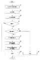
ここで、このように実施されるDRAM2を救済する処理について説明する。図4は、DRAM2を救済する処理の流れの例を説明するためのフローチャートである。 Here, the processing for relieving the
まず、ATE54からDRAM2のBISTを実行するための指示がTCU11に出力される(ステップS1)。この指示は、テストバス41を介してBIST回路42に供給され、BISTが実行される(ステップS2)。BISTの実行結果が、テスト結果保持部48、リペアブル情報保持部49及びアドレス情報保持部50のそれぞれに格納され(ステップS3)、テスト結果保持部48に格納された情報に基づいて、良品か否かが判定される(ステップS4)。良品の場合、YESとなり、ステップS10に進み、PASSと判定される。良品でない場合、NOとなり、リペアブル情報保持部49に格納された情報に基づいて、救済可能か否かが判定される(ステップS5)。救済可能でない場合、NOとなり、FAILと判定される(ステップS6)。救済可能な場合、YESとなり、リペア情報が読み出される(ステップS7)。ここで、リペア情報は、リペアブル情報保持部49及びアドレス情報保持部50のそれぞれに格納されている情報である。このリペア情報をeFuseマクロ13にブローするブロー処理が実行される(ステップS8)。ブローされた情報を利用したBISTが実行され(ステップS9)、PASSと判定される(ステップS10)。 First, an instruction for executing BIST of
なお、上述したように、ステップS8のブロー処理においてリペア情報が正しくブローされたことを確認すれば、ステップS9の処理を省略してもよい。これにより、ブロー処理後のBISTを省略し、テスト時間を短縮することができる。 As described above, if it is confirmed that the repair information has been correctly blown in the blow process in step S8, the process in step S9 may be omitted. As a result, the BIST after the blow processing can be omitted and the test time can be shortened.
以上の処理により、リペアブル情報保持部49及びアドレス情報保持部50のそれぞれに格納されたリペア情報、即ち、救済情報をeFuseマクロ13に格納する処理が完了する。 With the above processing, the processing for storing repair information stored in each of the repairable
次に、eFuseマクロ13にリペア情報がブローされた後の通常モードの動作について説明する。 Next, the operation in the normal mode after the repair information is blown to the
半導体装置1の電源が投入されると、POR回路32からセレクタ30に電源が投入されたことを示す信号が出力される。通常モードの場合、セレクタ30には、POR回路32の出力を選択するための選択信号がTUC11から供給される。セレクタ30は、この選択信号に基づいて、電源が投入されたことを示す信号をeFuseマクロ13に出力する。 When the power of the
eFuseマクロ13は、この信号が入力されると、ブローされた不良ビットのアドレス情報をセレクタ31を介してeFuseレジスタ12に書き込む。eFuseレジスタ12に格納されたアドレス情報は、アドレスコントローラ44に出力される。 When this signal is input, the
プロセッサコア16は、通常モード時にはデータの書き込みあるいは読み出し用のアドレスをバス17を介してアドレスコントローラ44に供給する。アドレスコントローラ44は、eFuseレジスタ12からのアドレスとデータ書き込み用のアドレスとが一致した場合、セレクタ43により選択されたバス17からのデータをリペアレジスタ51に書き込む処理を行う。また、アドレスコントローラ44は、eFuseレジスタ12からのアドレスとデータ読み出し用のアドレスとが一致した場合、リペアレジスタ51に格納されたデータを読み出す処理を行う。このように読み出されたデータは、セレクタ45を介してバス17に出力される。このように、プロセッサコア16は、DRAM2のビット不良のあるアドレスへのデータの書き込みまたは読み出しを行う場合、リペアレジスタ51へのデータの書き込みまたは読み出しを行うことになる。 The
なお、上述したeFuse回路13へのブロー処理を実行する前に、リペアブル情報保持部49及びアドレス情報保持部50に格納されたリペア情報を用いて、DRAM2のビット不良の救済が可能か否かを判定するようにしてもよい。このリペア情報をeFuseマクロ13にブローすると、eFuseマクロ13の内容は、変更することができない。そのため、リペア情報をeFuseマクロ13にブローする前に、このリペア情報を用いてDRAM2のビット不良の救済が可能か否かを判定し、可能と判定された後に、リペア情報をeFuseマクロ13にブローする。これにより、DRAM2のビット不良の救済が確実に行えるようになる。 Before executing the blow process to the
まず、TCU11は、リペアブル情報保持部49及びアドレス情報保持部50に格納されたリペア情報をeFuse端子33に出力する。eFuse端子33は、このリペア情報をセレクタ31に出力する。このとき、TCU11は、eFuse端子33からのリペア情報を選択するための選択信号をセレクタ31に出力する。セレクタ31は、この選択信号に基づいて、eFuse端子33からのリペア情報をeFuseレジスタ12に出力する。 First, the
これにより、例えば、イネーブル情報を示す“1”がリペアブル情報格納部12aに格納され、FAILしたアドレスのアドレス情報を示す“80”がアドレス情報格納部12bに格納される。ここで、上述したBISTを実行することにより、アドレスが“80”のときのデータの書き込み及び読み出しは、リペアレジスタ51を用いて行われることになる。このBIST結果、DRAM2のビット不良の救済が行われている場合、テスト結果保持部48には、テストのPASSを示す“1”が格納される。 Thereby, for example, “1” indicating enable information is stored in the repairable information storage unit 12a, and “80” indicating address information of the failed address is stored in the address information storage unit 12b. Here, by executing the BIST described above, writing and reading of data when the address is “80” is performed using the
TCU11は、テスト結果保持部48の情報に基づいて、テストをPASSしたと判定すると、eFuse端子33に出力したリペア情報をeFuseマクロ13にブローする。この結果、DRAM2のビット不良の救済が確実に行えるようになる。 If the
なお、本実施の形態において、DRAM I/O15及びDRAM2は同一の電源とする。半導体装置1は、消費電力を削減するため、例えば、スリープモード時に、半導体装置1内の大部分の回路の電源を落とす場合がある。このとき、DRAM2に保持されたデータの消去を防ぐため、DRAM2の電源は供給され、リペアレジスタ51に保持されたデータの消去を防ぐため、DRAM I/O15の電源も供給されている。ここで、DRAM I/O15の電源を半導体装置1内の他の回路と同一の電源にすると、スリープモード時に、リペアレジスタ51に保持されたデータが消去されてしまう。そのため、DRAM I/O15及びDRAM2は同一の電源とし、意図しないデータの消去を防ぐようにしている。 In this embodiment, the DRAM I /
以上のように、半導体装置1は、積層されたDRAM2の自己診断テストを実行し、DRAM2のビット不良のアドレス情報を検出するBIST回路42を設けた。BIST回路42により検出されたDRAM2のビット不良のアドレス情報は、eFuseマクロ13にブローされ、パワーオンリセット時にアドレスコントローラ44に出力される。アドレスコントローラ44は、ビット不良のアドレスへのデータの書き込みまたは読み出しが指示されると、リペアレジスタ51を使用し、データの書き込みまたは読み出しを行うように制御する。この結果、半導体装置1は、DRAM2のビット不良のアドレスへのデータの書き込みまたは読み出しを行う場合、リペアレジスタ51を使用するので、積層されているDRAM2が救済回路を有していなくても、ビット不良の救済ができる。 As described above, the
よって、本実施の形態の半導体装置によれば、接続されるメモリに救済回路が搭載されている否かに拘わらず、接続されるメモリの救済を容易に可能にすることができる。 Therefore, according to the semiconductor device of this embodiment, the connected memory can be easily relieved regardless of whether or not the relieved circuit is mounted on the connected memory.
なお、本明細書におけるフローチャート中の各ステップは、その性質に反しない限り、実行順序を変更し、複数同時に実行し、あるいは実行毎に異なった順序で実行してもよい。 Note that the steps in the flowcharts in this specification may be executed in a different order for each execution by changing the execution order and executing a plurality of steps at the same time, as long as the steps are not contrary to the nature.
本発明は、上述した実施の形態に限定されるものではなく、本発明の要旨を変えない範囲において、種々の変更、改変等が可能である。 The present invention is not limited to the above-described embodiments, and various changes and modifications can be made without departing from the scope of the present invention.
1…半導体装置、2…DRAM、3…半導体チップ、11…テストコントロールユニット、12…eFuseレジスタ、12a…リペアブル情報格納部、12b…アドレス情報格納部、13…eFuseマクロ、14…DRAM I/F、15…DRAM I/O、21…メモリセル、22…SRAM、23…eFuse、30,31…セレクタ、32…POR回路、33…eFuse端子、41…テストバス、42…BIST回路、43…セレクタ、44…アドレスコントローラ、45,46…セレクタ、47…パターンジェネレータ、48…テスト結果保持部、49…リペアブル情報保持部、50…アドレス情報保持部、51…リペアレジスタ、52,53…バッファ回路、54…ATE。 DESCRIPTION OF
Claims (5)
Translated fromJapanese前記半導体装置に接続されるメモリのビット不良を検出し、検出した前記ビット不良のアドレスを得るビット不良検出回路と、
前記ビット不良検出回路により検出された前記メモリの前記ビット不良のアドレスを保持する不揮発性の不良情報保持回路と、
前記ビット不良のアドレスのビット情報を記憶する不良対応用記憶回路と、
前記パワーオンリセット時に前記不良情報保持回路に保持されたアドレスに基づいて、前記ビット不良のアドレスへのリードおよびライト時に前記不良対応用記憶回路を使用するように制御する制御部と、
を有することを特徴とする半導体装置。A semiconductor device having a processor core that operates after a power-on reset,
A bit defect detection circuit for detecting a bit defect of a memory connected to the semiconductor device and obtaining an address of the detected bit defect;
A nonvolatile defect information holding circuit for holding an address of the bit defect of the memory detected by the bit defect detection circuit;
A failure handling memory circuit for storing bit information of an address of the bit failure;
Based on the address held in the failure information holding circuit at the time of power-on reset, a control unit that controls to use the failure handling storage circuit at the time of reading and writing to the address of the bit failure,
A semiconductor device comprising:
Priority Applications (2)
| Application Number | Priority Date | Filing Date | Title |
|---|---|---|---|
| JP2009024310AJP5127737B2 (en) | 2009-02-04 | 2009-02-04 | Semiconductor device |
| US12/694,475US8208325B2 (en) | 2009-02-04 | 2010-01-27 | Semiconductor device, semiconductor package and memory repair method |
Applications Claiming Priority (1)
| Application Number | Priority Date | Filing Date | Title |
|---|---|---|---|
| JP2009024310AJP5127737B2 (en) | 2009-02-04 | 2009-02-04 | Semiconductor device |
Publications (2)
| Publication Number | Publication Date |
|---|---|
| JP2010182366Atrue JP2010182366A (en) | 2010-08-19 |
| JP5127737B2 JP5127737B2 (en) | 2013-01-23 |
Family
ID=42397624
Family Applications (1)
| Application Number | Title | Priority Date | Filing Date |
|---|---|---|---|
| JP2009024310AExpired - Fee RelatedJP5127737B2 (en) | 2009-02-04 | 2009-02-04 | Semiconductor device |
Country Status (2)
| Country | Link |
|---|---|
| US (1) | US8208325B2 (en) |
| JP (1) | JP5127737B2 (en) |
Cited By (5)
| Publication number | Priority date | Publication date | Assignee | Title |
|---|---|---|---|---|
| US8130570B2 (en) | 2009-09-25 | 2012-03-06 | Kabushiki Kaisha Toshiba | Data transfer circuit |
| JP2012064282A (en)* | 2010-09-17 | 2012-03-29 | Elpida Memory Inc | Semiconductor device |
| JP2015515061A (en)* | 2012-03-30 | 2015-05-21 | インテル・コーポレーション | Built-in self-test for stacked memory architecture |
| US9236143B2 (en) | 2011-12-28 | 2016-01-12 | Intel Corporation | Generic address scrambler for memory circuit test engine |
| US10438929B2 (en) | 2014-09-17 | 2019-10-08 | Toshiba Memory Corporation | Semiconductor device |
Families Citing this family (8)
| Publication number | Priority date | Publication date | Assignee | Title |
|---|---|---|---|---|
| US9087613B2 (en) | 2012-02-29 | 2015-07-21 | Samsung Electronics Co., Ltd. | Device and method for repairing memory cell and memory system including the device |
| US8988956B2 (en)* | 2012-09-18 | 2015-03-24 | Mosys, Inc. | Programmable memory built in self repair circuit |
| KR102025341B1 (en) | 2012-12-04 | 2019-09-25 | 삼성전자 주식회사 | Memory controller, Memory system including the memory controller and Method of operating the memory controller |
| US9430324B2 (en)* | 2013-05-24 | 2016-08-30 | Rambus Inc. | Memory repair method and apparatus based on error code tracking |
| KR102152782B1 (en) | 2014-07-07 | 2020-09-07 | 삼성전자주식회사 | Methods for maunfacturing and operating memory device and method for operating thereof |
| KR102179829B1 (en) | 2014-07-10 | 2020-11-18 | 삼성전자주식회사 | Storage system managing run-time bad cells |
| KR20160119582A (en)* | 2015-04-06 | 2016-10-14 | 에스케이하이닉스 주식회사 | Memory device and operation method of the same |
| US20200176072A1 (en)* | 2020-02-04 | 2020-06-04 | Intel Corporation | Dynamic random access memory built-in self-test power fail mitigation |
Citations (4)
| Publication number | Priority date | Publication date | Assignee | Title |
|---|---|---|---|---|
| JP2004158098A (en)* | 2002-11-06 | 2004-06-03 | Renesas Technology Corp | System-in-package type semiconductor device |
| JP2007287292A (en)* | 2006-04-20 | 2007-11-01 | Renesas Technology Corp | Semiconductor integrated circuit device |
| JP2007335809A (en)* | 2006-06-19 | 2007-12-27 | Nec Electronics Corp | Semiconductor device and method for controlling operation of semiconductor device |
| JP2008269669A (en)* | 2007-04-17 | 2008-11-06 | Renesas Technology Corp | Semiconductor device and data processing system |
Family Cites Families (5)
| Publication number | Priority date | Publication date | Assignee | Title |
|---|---|---|---|---|
| JP2006186247A (en) | 2004-12-28 | 2006-07-13 | Nec Electronics Corp | Semiconductor device |
| US7053470B1 (en)* | 2005-02-19 | 2006-05-30 | Azul Systems, Inc. | Multi-chip package having repairable embedded memories on a system chip with an EEPROM chip storing repair information |
| JP4817701B2 (en)* | 2005-04-06 | 2011-11-16 | 株式会社東芝 | Semiconductor device |
| JP5165404B2 (en) | 2007-06-06 | 2013-03-21 | ルネサスエレクトロニクス株式会社 | Semiconductor device, semiconductor device manufacturing method and test method |
| US7768847B2 (en)* | 2008-04-09 | 2010-08-03 | Rambus Inc. | Programmable memory repair scheme |
- 2009
- 2009-02-04JPJP2009024310Apatent/JP5127737B2/ennot_activeExpired - Fee Related
- 2010
- 2010-01-27USUS12/694,475patent/US8208325B2/ennot_activeExpired - Fee Related
Patent Citations (4)
| Publication number | Priority date | Publication date | Assignee | Title |
|---|---|---|---|---|
| JP2004158098A (en)* | 2002-11-06 | 2004-06-03 | Renesas Technology Corp | System-in-package type semiconductor device |
| JP2007287292A (en)* | 2006-04-20 | 2007-11-01 | Renesas Technology Corp | Semiconductor integrated circuit device |
| JP2007335809A (en)* | 2006-06-19 | 2007-12-27 | Nec Electronics Corp | Semiconductor device and method for controlling operation of semiconductor device |
| JP2008269669A (en)* | 2007-04-17 | 2008-11-06 | Renesas Technology Corp | Semiconductor device and data processing system |
Cited By (6)
| Publication number | Priority date | Publication date | Assignee | Title |
|---|---|---|---|---|
| US8130570B2 (en) | 2009-09-25 | 2012-03-06 | Kabushiki Kaisha Toshiba | Data transfer circuit |
| JP2012064282A (en)* | 2010-09-17 | 2012-03-29 | Elpida Memory Inc | Semiconductor device |
| US9252062B2 (en) | 2010-09-17 | 2016-02-02 | Ps4 Luxco S.A.R.L. | Semiconductor device having optical fuse and electrical fuse |
| US9236143B2 (en) | 2011-12-28 | 2016-01-12 | Intel Corporation | Generic address scrambler for memory circuit test engine |
| JP2015515061A (en)* | 2012-03-30 | 2015-05-21 | インテル・コーポレーション | Built-in self-test for stacked memory architecture |
| US10438929B2 (en) | 2014-09-17 | 2019-10-08 | Toshiba Memory Corporation | Semiconductor device |
Also Published As
| Publication number | Publication date |
|---|---|
| JP5127737B2 (en) | 2013-01-23 |
| US8208325B2 (en) | 2012-06-26 |
| US20100195425A1 (en) | 2010-08-05 |
Similar Documents
| Publication | Publication Date | Title |
|---|---|---|
| JP5127737B2 (en) | Semiconductor device | |
| US7937631B2 (en) | Method for self-test and self-repair in a multi-chip package environment | |
| KR102117633B1 (en) | Self repair device | |
| TWI390541B (en) | Jtag controlled self-repair after packaging | |
| US7512001B2 (en) | Semiconductor memory device, test system including the same and repair method of semiconductor memory device | |
| CN101405818B (en) | Semiconductor memory and test system | |
| US8913451B2 (en) | Memory device and test method thereof | |
| JP2010225239A (en) | Semiconductor integrated circuit and memory functional verification method | |
| US20120230136A1 (en) | Selectable repair pass masking | |
| CN108511029B (en) | Built-in self-test and repair system and method for dual-port SRAM array in FPGA | |
| JP2010123159A (en) | Semiconductor integrated circuit | |
| US20130232386A1 (en) | Memory devices, testing systems and methods | |
| US8867288B2 (en) | Memory device and test method thereof | |
| US7549098B2 (en) | Redundancy programming for a memory device | |
| JP4824083B2 (en) | Semiconductor memory | |
| JP3967704B2 (en) | Semiconductor memory device and test method thereof | |
| KR101877939B1 (en) | Test circuit, memory system and test method of memory system | |
| JP2008262630A (en) | Semiconductor integrated circuit and memory inspection method | |
| JP4257342B2 (en) | Semiconductor memory device, memory module, and memory module inspection method | |
| KR20150006167A (en) | Semiconductor system and repair memthod of the same | |
| JP4761995B2 (en) | Semiconductor integrated circuit and test method thereof | |
| JP4351649B2 (en) | Semiconductor memory device | |
| JP3898390B2 (en) | Semiconductor memory device | |
| JP3938298B2 (en) | Memory circuit having parity cell array | |
| JP2013118034A (en) | Memory controller |
Legal Events
| Date | Code | Title | Description |
|---|---|---|---|
| A621 | Written request for application examination | Free format text:JAPANESE INTERMEDIATE CODE: A621 Effective date:20110222 | |
| A977 | Report on retrieval | Free format text:JAPANESE INTERMEDIATE CODE: A971007 Effective date:20120914 | |
| TRDD | Decision of grant or rejection written | ||
| A01 | Written decision to grant a patent or to grant a registration (utility model) | Free format text:JAPANESE INTERMEDIATE CODE: A01 Effective date:20121002 | |
| A01 | Written decision to grant a patent or to grant a registration (utility model) | Free format text:JAPANESE INTERMEDIATE CODE: A01 | |
| A61 | First payment of annual fees (during grant procedure) | Free format text:JAPANESE INTERMEDIATE CODE: A61 Effective date:20121030 | |
| FPAY | Renewal fee payment (event date is renewal date of database) | Free format text:PAYMENT UNTIL: 20151109 Year of fee payment:3 | |
| LAPS | Cancellation because of no payment of annual fees |