JP2010164989A - Optical crystal - Google Patents
Optical crystalDownload PDFInfo
- Publication number
- JP2010164989A JP2010164989AJP2010051141AJP2010051141AJP2010164989AJP 2010164989 AJP2010164989 AJP 2010164989AJP 2010051141 AJP2010051141 AJP 2010051141AJP 2010051141 AJP2010051141 AJP 2010051141AJP 2010164989 AJP2010164989 AJP 2010164989A
- Authority
- JP
- Japan
- Prior art keywords
- dispersion compensation
- dispersion
- layer
- optical crystal
- region
- Prior art date
- Legal status (The legal status is an assumption and is not a legal conclusion. Google has not performed a legal analysis and makes no representation as to the accuracy of the status listed.)
- Pending
Links
Images


Classifications
- G—PHYSICS
- G02—OPTICS
- G02F—OPTICAL DEVICES OR ARRANGEMENTS FOR THE CONTROL OF LIGHT BY MODIFICATION OF THE OPTICAL PROPERTIES OF THE MEDIA OF THE ELEMENTS INVOLVED THEREIN; NON-LINEAR OPTICS; FREQUENCY-CHANGING OF LIGHT; OPTICAL LOGIC ELEMENTS; OPTICAL ANALOGUE/DIGITAL CONVERTERS
- G02F1/00—Devices or arrangements for the control of the intensity, colour, phase, polarisation or direction of light arriving from an independent light source, e.g. switching, gating or modulating; Non-linear optics
- G02F1/01—Devices or arrangements for the control of the intensity, colour, phase, polarisation or direction of light arriving from an independent light source, e.g. switching, gating or modulating; Non-linear optics for the control of the intensity, phase, polarisation or colour
- G02F1/015—Devices or arrangements for the control of the intensity, colour, phase, polarisation or direction of light arriving from an independent light source, e.g. switching, gating or modulating; Non-linear optics for the control of the intensity, phase, polarisation or colour based on semiconductor elements having potential barriers, e.g. having a PN or PIN junction
- G02F1/025—Devices or arrangements for the control of the intensity, colour, phase, polarisation or direction of light arriving from an independent light source, e.g. switching, gating or modulating; Non-linear optics for the control of the intensity, phase, polarisation or colour based on semiconductor elements having potential barriers, e.g. having a PN or PIN junction in an optical waveguide structure
- B—PERFORMING OPERATIONS; TRANSPORTING
- B82—NANOTECHNOLOGY
- B82Y—SPECIFIC USES OR APPLICATIONS OF NANOSTRUCTURES; MEASUREMENT OR ANALYSIS OF NANOSTRUCTURES; MANUFACTURE OR TREATMENT OF NANOSTRUCTURES
- B82Y20/00—Nanooptics, e.g. quantum optics or photonic crystals
- G—PHYSICS
- G02—OPTICS
- G02B—OPTICAL ELEMENTS, SYSTEMS OR APPARATUS
- G02B6/00—Light guides; Structural details of arrangements comprising light guides and other optical elements, e.g. couplings
- G02B6/10—Light guides; Structural details of arrangements comprising light guides and other optical elements, e.g. couplings of the optical waveguide type
- G02B6/12—Light guides; Structural details of arrangements comprising light guides and other optical elements, e.g. couplings of the optical waveguide type of the integrated circuit kind
- G02B6/122—Basic optical elements, e.g. light-guiding paths
- G02B6/1225—Basic optical elements, e.g. light-guiding paths comprising photonic band-gap structures or photonic lattices
- G—PHYSICS
- G02—OPTICS
- G02F—OPTICAL DEVICES OR ARRANGEMENTS FOR THE CONTROL OF LIGHT BY MODIFICATION OF THE OPTICAL PROPERTIES OF THE MEDIA OF THE ELEMENTS INVOLVED THEREIN; NON-LINEAR OPTICS; FREQUENCY-CHANGING OF LIGHT; OPTICAL LOGIC ELEMENTS; OPTICAL ANALOGUE/DIGITAL CONVERTERS
- G02F1/00—Devices or arrangements for the control of the intensity, colour, phase, polarisation or direction of light arriving from an independent light source, e.g. switching, gating or modulating; Non-linear optics
- G02F1/01—Devices or arrangements for the control of the intensity, colour, phase, polarisation or direction of light arriving from an independent light source, e.g. switching, gating or modulating; Non-linear optics for the control of the intensity, phase, polarisation or colour
- G02F1/03—Devices or arrangements for the control of the intensity, colour, phase, polarisation or direction of light arriving from an independent light source, e.g. switching, gating or modulating; Non-linear optics for the control of the intensity, phase, polarisation or colour based on ceramics or electro-optical crystals, e.g. exhibiting Pockels effect or Kerr effect
- G02F1/0305—Constructional arrangements
- G—PHYSICS
- G02—OPTICS
- G02F—OPTICAL DEVICES OR ARRANGEMENTS FOR THE CONTROL OF LIGHT BY MODIFICATION OF THE OPTICAL PROPERTIES OF THE MEDIA OF THE ELEMENTS INVOLVED THEREIN; NON-LINEAR OPTICS; FREQUENCY-CHANGING OF LIGHT; OPTICAL LOGIC ELEMENTS; OPTICAL ANALOGUE/DIGITAL CONVERTERS
- G02F1/00—Devices or arrangements for the control of the intensity, colour, phase, polarisation or direction of light arriving from an independent light source, e.g. switching, gating or modulating; Non-linear optics
- G02F1/01—Devices or arrangements for the control of the intensity, colour, phase, polarisation or direction of light arriving from an independent light source, e.g. switching, gating or modulating; Non-linear optics for the control of the intensity, phase, polarisation or colour
- G02F1/03—Devices or arrangements for the control of the intensity, colour, phase, polarisation or direction of light arriving from an independent light source, e.g. switching, gating or modulating; Non-linear optics for the control of the intensity, phase, polarisation or colour based on ceramics or electro-optical crystals, e.g. exhibiting Pockels effect or Kerr effect
- G02F1/035—Devices or arrangements for the control of the intensity, colour, phase, polarisation or direction of light arriving from an independent light source, e.g. switching, gating or modulating; Non-linear optics for the control of the intensity, phase, polarisation or colour based on ceramics or electro-optical crystals, e.g. exhibiting Pockels effect or Kerr effect in an optical waveguide structure
- H—ELECTRICITY
- H04—ELECTRIC COMMUNICATION TECHNIQUE
- H04B—TRANSMISSION
- H04B10/00—Transmission systems employing electromagnetic waves other than radio-waves, e.g. infrared, visible or ultraviolet light, or employing corpuscular radiation, e.g. quantum communication
- H04B10/25—Arrangements specific to fibre transmission
- H04B10/2507—Arrangements specific to fibre transmission for the reduction or elimination of distortion or dispersion
- H04B10/2513—Arrangements specific to fibre transmission for the reduction or elimination of distortion or dispersion due to chromatic dispersion
- H04B10/25133—Arrangements specific to fibre transmission for the reduction or elimination of distortion or dispersion due to chromatic dispersion including a lumped electrical or optical dispersion compensator
- G—PHYSICS
- G02—OPTICS
- G02F—OPTICAL DEVICES OR ARRANGEMENTS FOR THE CONTROL OF LIGHT BY MODIFICATION OF THE OPTICAL PROPERTIES OF THE MEDIA OF THE ELEMENTS INVOLVED THEREIN; NON-LINEAR OPTICS; FREQUENCY-CHANGING OF LIGHT; OPTICAL LOGIC ELEMENTS; OPTICAL ANALOGUE/DIGITAL CONVERTERS
- G02F1/00—Devices or arrangements for the control of the intensity, colour, phase, polarisation or direction of light arriving from an independent light source, e.g. switching, gating or modulating; Non-linear optics
- G02F1/01—Devices or arrangements for the control of the intensity, colour, phase, polarisation or direction of light arriving from an independent light source, e.g. switching, gating or modulating; Non-linear optics for the control of the intensity, phase, polarisation or colour
- G02F1/0128—Devices or arrangements for the control of the intensity, colour, phase, polarisation or direction of light arriving from an independent light source, e.g. switching, gating or modulating; Non-linear optics for the control of the intensity, phase, polarisation or colour based on electro-mechanical, magneto-mechanical, elasto-optic effects
- G02F1/0131—Devices or arrangements for the control of the intensity, colour, phase, polarisation or direction of light arriving from an independent light source, e.g. switching, gating or modulating; Non-linear optics for the control of the intensity, phase, polarisation or colour based on electro-mechanical, magneto-mechanical, elasto-optic effects based on photo-elastic effects, e.g. mechanically induced birefringence
- G02F1/0134—Devices or arrangements for the control of the intensity, colour, phase, polarisation or direction of light arriving from an independent light source, e.g. switching, gating or modulating; Non-linear optics for the control of the intensity, phase, polarisation or colour based on electro-mechanical, magneto-mechanical, elasto-optic effects based on photo-elastic effects, e.g. mechanically induced birefringence in optical waveguides
- G—PHYSICS
- G02—OPTICS
- G02F—OPTICAL DEVICES OR ARRANGEMENTS FOR THE CONTROL OF LIGHT BY MODIFICATION OF THE OPTICAL PROPERTIES OF THE MEDIA OF THE ELEMENTS INVOLVED THEREIN; NON-LINEAR OPTICS; FREQUENCY-CHANGING OF LIGHT; OPTICAL LOGIC ELEMENTS; OPTICAL ANALOGUE/DIGITAL CONVERTERS
- G02F1/00—Devices or arrangements for the control of the intensity, colour, phase, polarisation or direction of light arriving from an independent light source, e.g. switching, gating or modulating; Non-linear optics
- G02F1/01—Devices or arrangements for the control of the intensity, colour, phase, polarisation or direction of light arriving from an independent light source, e.g. switching, gating or modulating; Non-linear optics for the control of the intensity, phase, polarisation or colour
- G02F1/0147—Devices or arrangements for the control of the intensity, colour, phase, polarisation or direction of light arriving from an independent light source, e.g. switching, gating or modulating; Non-linear optics for the control of the intensity, phase, polarisation or colour based on thermo-optic effects
- G—PHYSICS
- G02—OPTICS
- G02F—OPTICAL DEVICES OR ARRANGEMENTS FOR THE CONTROL OF LIGHT BY MODIFICATION OF THE OPTICAL PROPERTIES OF THE MEDIA OF THE ELEMENTS INVOLVED THEREIN; NON-LINEAR OPTICS; FREQUENCY-CHANGING OF LIGHT; OPTICAL LOGIC ELEMENTS; OPTICAL ANALOGUE/DIGITAL CONVERTERS
- G02F1/00—Devices or arrangements for the control of the intensity, colour, phase, polarisation or direction of light arriving from an independent light source, e.g. switching, gating or modulating; Non-linear optics
- G02F1/01—Devices or arrangements for the control of the intensity, colour, phase, polarisation or direction of light arriving from an independent light source, e.g. switching, gating or modulating; Non-linear optics for the control of the intensity, phase, polarisation or colour
- G02F1/015—Devices or arrangements for the control of the intensity, colour, phase, polarisation or direction of light arriving from an independent light source, e.g. switching, gating or modulating; Non-linear optics for the control of the intensity, phase, polarisation or colour based on semiconductor elements having potential barriers, e.g. having a PN or PIN junction
- G02F1/0151—Devices or arrangements for the control of the intensity, colour, phase, polarisation or direction of light arriving from an independent light source, e.g. switching, gating or modulating; Non-linear optics for the control of the intensity, phase, polarisation or colour based on semiconductor elements having potential barriers, e.g. having a PN or PIN junction modulating the refractive index
- G02F1/0152—Devices or arrangements for the control of the intensity, colour, phase, polarisation or direction of light arriving from an independent light source, e.g. switching, gating or modulating; Non-linear optics for the control of the intensity, phase, polarisation or colour based on semiconductor elements having potential barriers, e.g. having a PN or PIN junction modulating the refractive index using free carrier effects, e.g. plasma effect
- G—PHYSICS
- G02—OPTICS
- G02F—OPTICAL DEVICES OR ARRANGEMENTS FOR THE CONTROL OF LIGHT BY MODIFICATION OF THE OPTICAL PROPERTIES OF THE MEDIA OF THE ELEMENTS INVOLVED THEREIN; NON-LINEAR OPTICS; FREQUENCY-CHANGING OF LIGHT; OPTICAL LOGIC ELEMENTS; OPTICAL ANALOGUE/DIGITAL CONVERTERS
- G02F1/00—Devices or arrangements for the control of the intensity, colour, phase, polarisation or direction of light arriving from an independent light source, e.g. switching, gating or modulating; Non-linear optics
- G02F1/01—Devices or arrangements for the control of the intensity, colour, phase, polarisation or direction of light arriving from an independent light source, e.g. switching, gating or modulating; Non-linear optics for the control of the intensity, phase, polarisation or colour
- G02F1/03—Devices or arrangements for the control of the intensity, colour, phase, polarisation or direction of light arriving from an independent light source, e.g. switching, gating or modulating; Non-linear optics for the control of the intensity, phase, polarisation or colour based on ceramics or electro-optical crystals, e.g. exhibiting Pockels effect or Kerr effect
- G02F1/0305—Constructional arrangements
- G02F1/0322—Arrangements comprising two or more independently controlled crystals
- G—PHYSICS
- G02—OPTICS
- G02F—OPTICAL DEVICES OR ARRANGEMENTS FOR THE CONTROL OF LIGHT BY MODIFICATION OF THE OPTICAL PROPERTIES OF THE MEDIA OF THE ELEMENTS INVOLVED THEREIN; NON-LINEAR OPTICS; FREQUENCY-CHANGING OF LIGHT; OPTICAL LOGIC ELEMENTS; OPTICAL ANALOGUE/DIGITAL CONVERTERS
- G02F2202/00—Materials and properties
- G02F2202/10—Materials and properties semiconductor
- G02F2202/105—Materials and properties semiconductor single crystal Si
- G—PHYSICS
- G02—OPTICS
- G02F—OPTICAL DEVICES OR ARRANGEMENTS FOR THE CONTROL OF LIGHT BY MODIFICATION OF THE OPTICAL PROPERTIES OF THE MEDIA OF THE ELEMENTS INVOLVED THEREIN; NON-LINEAR OPTICS; FREQUENCY-CHANGING OF LIGHT; OPTICAL LOGIC ELEMENTS; OPTICAL ANALOGUE/DIGITAL CONVERTERS
- G02F2202/00—Materials and properties
- G02F2202/32—Photonic crystals
- G—PHYSICS
- G02—OPTICS
- G02F—OPTICAL DEVICES OR ARRANGEMENTS FOR THE CONTROL OF LIGHT BY MODIFICATION OF THE OPTICAL PROPERTIES OF THE MEDIA OF THE ELEMENTS INVOLVED THEREIN; NON-LINEAR OPTICS; FREQUENCY-CHANGING OF LIGHT; OPTICAL LOGIC ELEMENTS; OPTICAL ANALOGUE/DIGITAL CONVERTERS
- G02F2203/00—Function characteristic
- G02F2203/05—Function characteristic wavelength dependent
- G—PHYSICS
- G02—OPTICS
- G02F—OPTICAL DEVICES OR ARRANGEMENTS FOR THE CONTROL OF LIGHT BY MODIFICATION OF THE OPTICAL PROPERTIES OF THE MEDIA OF THE ELEMENTS INVOLVED THEREIN; NON-LINEAR OPTICS; FREQUENCY-CHANGING OF LIGHT; OPTICAL LOGIC ELEMENTS; OPTICAL ANALOGUE/DIGITAL CONVERTERS
- G02F2203/00—Function characteristic
- G02F2203/26—Pulse shaping; Apparatus or methods therefor
Landscapes
- Physics & Mathematics (AREA)
- Nonlinear Science (AREA)
- Engineering & Computer Science (AREA)
- Optics & Photonics (AREA)
- General Physics & Mathematics (AREA)
- Chemical & Material Sciences (AREA)
- Crystallography & Structural Chemistry (AREA)
- Ceramic Engineering (AREA)
- Nanotechnology (AREA)
- Biophysics (AREA)
- Life Sciences & Earth Sciences (AREA)
- Microelectronics & Electronic Packaging (AREA)
- Electromagnetism (AREA)
- Computer Networks & Wireless Communication (AREA)
- Signal Processing (AREA)
- Optical Integrated Circuits (AREA)
- Optical Modulation, Optical Deflection, Nonlinear Optics, Optical Demodulation, Optical Logic Elements (AREA)
- Optical Communication System (AREA)
- Optical Fibers, Optical Fiber Cores, And Optical Fiber Bundles (AREA)
Abstract
Description
Translated fromJapanese本発明は、光パルス伝送の際に生じる波長分散を補償する分散補償素子、分散補償システム等に関する。 The present invention relates to a dispersion compensation element, a dispersion compensation system, and the like that compensate for chromatic dispersion that occurs during optical pulse transmission.
近年、データ通信は光ファイバを介したものに移行しつつあり、これに伴い、データの伝送速度も従来より飛躍的に高まっている。
近い将来、このような光ファイバを介したデータ通信において、超短光パルスを用い、現時点での伝送速度より遥かに高速な160Gbit/sもしくはそれ以上の伝送速度で通信を行うことが検討されている。In recent years, data communication has been shifting to one via an optical fiber, and along with this, the data transmission speed has been dramatically increased.
In the near future, in data communication via such an optical fiber, it is considered to use ultrashort light pulses and perform communication at a transmission speed of 160 Gbit / s or higher, which is much higher than the current transmission speed. Yes.
ところで、データ通信を行う場合、常にクロストークや伝送エラーという問題がついて回るが、データの伝送速度が高まると、自ずと個々の光パルスの幅と、互いに前後する光パルスの間隔が狭まってくるため、この問題は非常に重要な問題となる。
光が物質中を進行する速度は、物質の屈折率で決まり、屈折率が大きいほど光速度は遅くなる。ガラス、半導体、光学結晶等の物質では、屈折率は光の周波数(空気中の波長)によって変化するため、光速度は波長に依存することになる。この、屈折率の波長依存性により、光パルスが物質中を進行する間に光パルスの波形を歪ませ、パルスの時間幅が広がる要因となることが知られている。このように、光の波長に応じて光速度が異なる、という特性を、以下、波長分散、あるいは単に分散と称する。By the way, when performing data communication, there are always problems such as crosstalk and transmission errors. However, as the data transmission speed increases, the width of each optical pulse and the interval between the optical pulses before and after each other are reduced. This problem becomes a very important problem.
The speed at which light travels through the material is determined by the refractive index of the material, and the higher the refractive index, the slower the light speed. In materials such as glass, semiconductors, and optical crystals, the refractive index changes depending on the frequency of light (wavelength in air), so the speed of light depends on the wavelength. It is known that due to the wavelength dependency of the refractive index, the waveform of the light pulse is distorted while the light pulse travels through the substance, and the time width of the pulse is widened. Thus, the characteristic that the speed of light differs according to the wavelength of light is hereinafter referred to as wavelength dispersion or simply dispersion.
上記のようにして、光ファイバ中を進行する間に、光パルスの波形が歪んだり、光パルスの時間幅が広がるわけであるが、従来の伝送速度では光パルスの時間幅も大きいため、特に大きな問題とはならない。しかし、データの伝送速度が高まると、前後の光パルスどうしが干渉するなどして、クロストークや伝送エラーが生じてしまう。このため、現状の技術のままで単に伝送速度を高めようとしたのでは、より高速度でのデータ通信は実現できないのである。
このような問題に対し、例えばフォトニック結晶を用い、波長分散を補償するという試みが既に行われている。As described above, while traveling in the optical fiber, the waveform of the optical pulse is distorted or the time width of the optical pulse is widened. It is not a big problem. However, when the data transmission rate increases, crosstalk and transmission errors occur due to interference between the front and rear optical pulses. For this reason, simply trying to increase the transmission speed with the current technology cannot realize data communication at a higher speed.
For such a problem, an attempt has been made to compensate for chromatic dispersion by using, for example, a photonic crystal.
フォトニック結晶は、屈折率が異なる二つの物質を周期的に配列した構造を有しており、この配列の一部を欠陥させて欠陥導波路(連続欠落部)を形成することで、特定の周波数の光のみが通過し、この光に対して特定の波長分散を与える導波モードが発生する。この導波モードを利用することで、光ファイバ伝送路の波長分散を補償するのである(例えば、非特許文献1参照)。
この他、フォトニック結晶と類似する構造として、光ファイバ回折格子を分散補償素子として利用する技術が実施されている。回折格子の周期を光ファイバの長手方向に沿って変化させたチャープ光ファイバ回折格子を用い、広いスペクトル帯域での波長分散を補償するという試みである(例えば、非特許文献2参照)。
また、理化学用の超短パルスレーザーが発生する光パルスを対象とした分散補償について、プリズム対や回折格子対を用いた技術が普及している。これらは、主として正の波長分散を補償するものである(例えば、非特許文献3参照)。A photonic crystal has a structure in which two substances having different refractive indexes are periodically arranged. A defect waveguide (continuous missing portion) is formed by defecting a part of this arrangement, and a specific waveguide is formed. Only light of a frequency passes, and a waveguide mode giving specific chromatic dispersion to this light is generated. By utilizing this waveguide mode, the chromatic dispersion of the optical fiber transmission line is compensated (see, for example, Non-Patent Document 1).
In addition, as a structure similar to a photonic crystal, a technique of using an optical fiber diffraction grating as a dispersion compensation element has been implemented. This is an attempt to compensate for chromatic dispersion in a wide spectral band by using a chirped optical fiber diffraction grating in which the period of the diffraction grating is changed along the longitudinal direction of the optical fiber (see, for example, Non-Patent Document 2).
In addition, a technique using a prism pair or a diffraction grating pair is widely used for dispersion compensation for an optical pulse generated by an ultrashort pulse laser for physics and chemistry. These mainly compensate for positive chromatic dispersion (see, for example, Non-Patent Document 3).
しかしながら、上記したような従来の波長分散補償技術を単純に用いたのでは、伝送速度のさらなる高速化には十分に対応しきれないという問題がある。
すなわち、波長分散は、前述したように光パルスの位相の波長(もしくは周波数、以下、単に波長と称する)依存性に起因するものである。一般に、光波の位相は、ある波長を中心として、波長の次数(べき指数)の異なる項によって展開された多項式として表される。2次の項の係数が最低次の波長分散に対応し、それに続く次数項の係数として、3次、4次、5次と続くことが知られている(例えば、非特許文献4参照)。However, if the conventional chromatic dispersion compensation technique as described above is simply used, there is a problem that the transmission speed cannot be sufficiently increased.
That is, chromatic dispersion is caused by the dependency of the phase of the optical pulse on the wavelength (or frequency, hereinafter simply referred to as wavelength) as described above. In general, the phase of a light wave is expressed as a polynomial developed by terms having different wavelength orders (power exponents) around a certain wavelength. It is known that the coefficient of the second-order term corresponds to the lowest-order chromatic dispersion, and the coefficient of the subsequent order term continues to the third-order, fourth-order, and fifth-order (for example, see Non-Patent Document 4).
現状の光パルスの伝送速度では、2次の項に対して波長分散を補償すれば十分であったが、伝送速度が高まるにつれて、データ送信に使用する光パルスの時間幅はより短くなり、それに反比例して光パルスのスペクトル幅は増加する。したがって、伝送速度が上昇するほど、広いスペクトル帯域にわたり、より高次までの波長分散係数を補償しなければ、光パルスの波形の歪を除去することはできない。
ところが、フォトニック結晶あるいは光ファイバ回折格子を用いた従来の波長分散補償技術では、2次、3次、4次等、個々の次数に対し、波長分散を補償することができるものの、複数の次数に対し、波長分散を補償することはできなかった。これでは広いスペクトル帯域を利用する超高速大容量光通信に対応する波長分散補償は実現できない。At the current transmission rate of the optical pulse, it was sufficient to compensate the chromatic dispersion for the second-order term. However, as the transmission rate increases, the time width of the optical pulse used for data transmission becomes shorter. The spectral width of the light pulse increases in inverse proportion. Therefore, as the transmission speed increases, the distortion of the waveform of the optical pulse cannot be removed unless the chromatic dispersion coefficients up to higher orders are compensated over a wide spectral band.
However, in the conventional chromatic dispersion compensation technique using a photonic crystal or an optical fiber diffraction grating, although chromatic dispersion can be compensated for individual orders such as second order, third order, and fourth order, a plurality of orders. On the other hand, chromatic dispersion could not be compensated. This makes it impossible to realize chromatic dispersion compensation corresponding to ultrahigh-speed and large-capacity optical communication using a wide spectrum band.
ところで、超高速大容量の光ファイバ伝送路は、それ自体で光パルスの伝送特性が最適となるように設計される。すなわち、伝送路全体として波長分散がゼロとなるように構成される。
しかし、例えば海底等に敷設される光ファイバ伝送路は、温度・気圧・振動等の影響により、光ファイバ伝送路が最適化された条件から外れることがある。そのような状況では、光ファイバ伝送路における波長分散は、正負の間を絶え間なく変化する。
これに対し、従来の技術では波長分散が正負に変化する場合において、波長分散補償の符号を波長分散の絶対値と独立に可変することは困難であった。このことは、波長分散値がゼロの付近で正負の間を絶え間なく変化するような状況に対応することが困難であることを意味する。
なお、「正」の波長分散とは、波長が長くなるほど光速度が増すことを指し、「負」の波長分散とは、波長が長くなるほど光速度が減少することを指している。By the way, the ultrahigh-speed and large-capacity optical fiber transmission line is designed so that the optical pulse transmission characteristics are optimized by itself. That is, the entire transmission line is configured to have zero chromatic dispersion.
However, an optical fiber transmission line laid on the seabed, for example, may deviate from the optimized conditions for the optical fiber transmission line due to the influence of temperature, atmospheric pressure, vibration, and the like. In such a situation, the chromatic dispersion in the optical fiber transmission line changes continuously between positive and negative.
On the other hand, in the conventional technique, when the chromatic dispersion changes between positive and negative, it is difficult to vary the sign of chromatic dispersion compensation independently of the absolute value of chromatic dispersion. This means that it is difficult to cope with a situation in which the chromatic dispersion value constantly changes between positive and negative in the vicinity of zero.
“Positive” chromatic dispersion means that the light velocity increases as the wavelength becomes longer, and “negative” chromatic dispersion means that the light velocity decreases as the wavelength becomes longer.
本発明は、このような技術的課題に基づいてなされたもので、光パルスの伝送速度の高速化を実現することのできる光学結晶を提供することを目的とする。 The present invention has been made based on such a technical problem, and an object thereof is to provide an optical crystal capable of realizing an increase in the transmission speed of an optical pulse.
本発明の光学結晶は、誘電率の異なる二つの物質を、交互に周期的に配列することで形成された周期配列層を含み、この周期配列層は、一方の物質中に周期的に配列される他方の物質が連続して欠落した連続欠落部が形成されるとともに、連続欠落部が連続する方向において、一方の物質中における他方の物質の周期配列特性が異なる複数の領域が形成されていることを特徴とする。
ここで、周期配列特性には、一方の物質中に配列される他方の物質のサイズや間隔等がある。The optical crystal of the present invention includes a periodic arrangement layer formed by alternately and periodically arranging two substances having different dielectric constants, and this periodic arrangement layer is periodically arranged in one substance. A continuous missing portion is formed in which the other material is continuously missing, and in the direction in which the continuous missing portion is continuous, a plurality of regions having different periodic arrangement characteristics of the other substance in one material are formed. It is characterized by that.
Here, the periodic arrangement characteristics include the size and interval of the other substance arranged in one substance.
このような周期配列層にて、複数の領域は、連続欠落部を光パルスが通過するとき、光パルスに与える波長分散の絶対値または符号が互いに異なるようにするのが好ましい。
また、周期配列層に、この周期配列層を形成する一方の物質とは屈折率が異なる物質で形成された他の層を積層することで、光学結晶を形成することもできる。In such a periodic array layer, it is preferable that the plurality of regions have different absolute values or signs of chromatic dispersion given to the optical pulse when the optical pulse passes through the continuous missing portion.
An optical crystal can also be formed by laminating another layer formed of a material having a refractive index different from that of one material forming the periodic array layer in the periodic array layer.
ところで、連続欠落部は、周期配列層に、三次元状に形成してもよいが、設計や製造の容易性を高めるには、二次元状に形成するのが好ましい。同様の理由から、連続欠落部は、周期配列層の一端側から他端側に向けて直線状に形成するのが好ましい。 By the way, although the continuous missing portion may be formed in the three-dimensional shape in the periodic arrangement layer, it is preferable to form the two-dimensional shape in order to improve the ease of design and manufacture. For the same reason, the continuous missing portion is preferably formed linearly from one end side to the other end side of the periodic array layer.
また、周期配列層に、連続欠落部とはキャリア密度が異なる異密度領域を形成しても良い。その場合、異密度領域は、連続欠落部よりもキャリア密度を高くするのが好ましい。
このような異密度領域には、周期配列層に電圧を印加するための電極が接続される。つまり、この異密度領域は端子部として機能するのである。その場合、電気抵抗を抑制するため、異密度領域は、前記の複数の領域よりも大きな面積とするのが好ましい。Moreover, you may form the different density area | region in which a carrier density differs from a continuous missing part in a periodic arrangement layer. In that case, the different density region preferably has a higher carrier density than the continuous missing portion.
An electrode for applying a voltage to the periodic array layer is connected to such a different density region. That is, this different density region functions as a terminal portion. In that case, in order to suppress electrical resistance, it is preferable that the different density region has a larger area than the plurality of regions.
本発明によれば、複数の領域を設けることで、例えば、正負の分散補償や、複数次の分散補償を行うことができる。また、各領域における波長分散を変動させることで、波長分散補償の絶対値と符号を可変することが可能となる。
また、電圧を印加することによって導波路のキャリア密度を変動させ、導波路の屈折率を変化させることによっても、分散補償を行うことができる。
そして、光ファイバ伝送路から取り出した光パルスをモニタリングし、その波長分散情報に基づき、波長分散を制御することで、光ファイバ伝送路において、温度、気象等による条件変動が生じても、常に最適な分散補償を行うことができる。
その結果、広いスペクトル帯域を利用する超高速大容量光通信に対応する波長分散補償を実現することができ、伝送速度のさらなる高速化を十分に実現することが可能となる。According to the present invention, by providing a plurality of regions, for example, positive / negative dispersion compensation or multiple-order dispersion compensation can be performed. Further, by changing the chromatic dispersion in each region, it is possible to vary the absolute value and the sign of the chromatic dispersion compensation.
Dispersion compensation can also be performed by changing the carrier density of the waveguide by applying a voltage and changing the refractive index of the waveguide.
And, by monitoring the optical pulse taken out from the optical fiber transmission line and controlling the chromatic dispersion based on the chromatic dispersion information, it is always optimal even if the optical fiber transmission line changes in conditions due to temperature, weather, etc. Dispersion compensation can be performed.
As a result, it is possible to realize chromatic dispersion compensation corresponding to ultrahigh-speed and large-capacity optical communication using a wide spectrum band, and it is possible to sufficiently realize further increase in transmission speed.
以下、添付図面に示す実施の形態に基づいてこの発明を詳細に説明する。 Hereinafter, the present invention will be described in detail based on embodiments shown in the accompanying drawings.
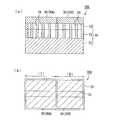
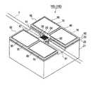
図1は、本実施の形態における分散補償システムを構成する分散補償素子の概略構成を説明するための図である。
この図1、図2に示すように、分散補償素子(分散補償部)10Xは、フォトニック結晶部20と、フォトニック結晶部20の一面側に設けられた電極(分散変動手段、エネルギー付与部材)30とを備えている。
フォトニック結晶部20は、基板21上に、クラッド層(他の層)22と、コア層(周期配列層)23とが積層されたもので、基板21は例えばシリコン(Si)で形成され、クラッド層22はシリコン酸化膜(SiO2)または窒化シリコン膜、コア層23は誘電体であるシリコン結晶(Si)で形成されている。
ここで、基板21には、導電性を持たせるため、不純物が添加されている。FIG. 1 is a diagram for explaining a schematic configuration of a dispersion compensation element constituting the dispersion compensation system according to the present embodiment.
As shown in FIGS. 1 and 2, the dispersion compensation element (dispersion compensation unit) 10X includes a
The
Here, impurities are added to the
また、図3に示すように、コア層23は、周期的に孔24が形成されている。これにより、コア層23は、コア層23の母材(例えばSi)と孔24の部分を満たす物質(一般には空気等の気体、他の物質を充填しても良い)により、誘電率(屈折率)の異なる2種類の物質が交互に周期的に配列されることで形成されている。
なお、図3において、孔24はコア層23だけでなく、クラッド層22にまで形成されているが、これは製造上の理由によるものであり、少なくともコア層23にのみ形成されていれば良い。Moreover, as shown in FIG. 3, the
In FIG. 3, the
コア層23に形成された孔24は、所定の半径(サイズ)rを有し、正三角形を単位胞とする三角格子状に配列され、各単位胞における孔24どうしは所定の間隔(正三角形の一辺の長さ)aを隔てている。
そして、このコア層23は、上記した孔24の半径rと、間隔aとが異なって設定された、領域(I)、(II)を備えている。
このようなコア層23には、領域(I)、(II)を貫通する方向において直線状に連続するよう、孔24が欠損する(孔24を形成しない)ことで、いわゆる欠陥導波路(導波路、連続欠落部)25が形成されている。The
The
In such a
このような構成のフォトニック結晶部20では、コア層23の上下面にて、屈折率が異なる他の物質(下面側にクラッド層22、上面側は空気)が存在することで、欠陥導波路25の一端側の入射端から入射した光はコア層23の上下面で反射しながら伝播し、欠陥導波路25の他端側の出射端から出射する。光が欠陥導波路25を伝播するとき、コア層23の領域(I)を伝播する間に、この領域(I)の孔24の半径rと間隔aに応じた波長分散を受け、続いて領域(II)を伝播する間に、この領域(II)の孔24の半径rと間隔aに応じた波長分散を受ける。つまり、このコア層23の欠陥導波路25から出射した光は、領域(I)と(II)を合成した波長分散を受けるのである。 In the
さて、図1および図2に示したように、フォトニック結晶部20の一面側、具体的には基板21ではなくコア層23に対向する側には、電極30が設けられている。この電極30は、コア層23の屈折率を変化させるエネルギーを外部から付与するためのものである。本実施の形態では、電極30として、前記の領域(I)と(II)に対応して独立して電極30A、30Bが設けられている。
そして、電極30A、30Bには、外部に、電源(図示無し)と、電源での電圧印加量をコントロールするコントローラ(図示無し)とが接続されるようになっており、これにより、分散変動手段が構成される。As shown in FIGS. 1 and 2, the
A power source (not shown) and a controller (not shown) for controlling the amount of voltage applied by the power source are connected to the
電極30A、30Bと、導電性を有した基板21との間に電圧(バイアス電圧)を印加すると、印加された電圧に応じてコア層23の領域(I)と(II)の屈折率が変化する。これを利用し、コントローラで、領域(I)の電極30Aと領域(II)の電極30Bとに電源から印加する電圧を個別に制御することで、領域(I)、(II)で与える波長分散を独立して変動させ、これにより最適な分散補償を行うのである。 When a voltage (bias voltage) is applied between the
ここで、上記したような分散補償素子10Xの、好ましい例を具体的に示す。
前述したように、フォトニック結晶部20の基板21は、導電性を有するために不純物を含有したシリコン(Si)で形成し、クラッド層22はシリコン酸化膜(SiO2)または窒化シリコン、コア層23は誘電体であるシリコン結晶(Si)で形成した。そして、クラッド層22とコア層23の厚みは、各々1000nmおよび220nmとした。このクラッド層22とコア層23の厚みは、欠陥導波路25の横モードが単一となる条件(横電界(transverse electric,TE)偏光に対して23nm以上かつ240nm以下)にある。
空気、コア層23、クラッド層22の屈折率を、各々nair、ncore、ncladと表すると、nair=1.00、ncore=3.50、nclad=1.45とした。Here, a preferable example of the
As described above, the
When the refractive indexes of air, the
このようなフォトニック結晶部20は、コア層23を形成する材料の上にレジストを塗布し、フォトリソグラフィ等の手法により所定の孔24のパターンをレジスト上に形成する。そして、ドライエッチングによりコア層23を形成する材料上に欠陥導波路25を形成するための孔24のパターンを形成する。ここで、孔24の部分は、空気とした。
孔24の配列は、正三角形を単位胞とする三角格子とし、領域(I)および(II)で周期を異ならせた。領域(I)ではa=493nmとし、領域(II)ではa=473nmとした。各々の領域とも、r/a=0.4となるように半径rを設定した。また、領域(I)および(II)の境界で隣接する孔24間の間隔d(図1参照)は、三角格子の周期の大きいほうの値、すなわち473nmより短くする。光が伝搬する欠陥導波路25は、線分P1−P2を中心としてそれに沿って構成された直線状とし、この欠陥導波路25は領域(I)の孔24が一つ分埋められた(欠陥した)ことにより形成される。領域(II)の欠陥導波路25の幅は領域(I)と等しく取られている。領域(I)、(II)それぞれにおける欠陥導波路25の長さは100μm、分散補償素子10Xでの欠陥導波路25のトータル長さは200μmとした。In such a
The
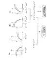
さて、図4に示すものは分散補償素子10Xにおける分散補償の原理を説明するための図である。
フォトニック結晶部20の領域(I)および(II)は、各々図4に示した光波伝搬を特徴付けるバンド特性を有する。欠陥導波路25中では、曲率の符号が異なる分枝1および2の導波モードがフォトニックギャップ中に形成される。
図4のグラフの縦軸および横軸は、1/aで規格化した光の周波数および波数である。導波モードは横電界(transverse electric,TE)偏光状態にある。欠陥導波路25中では、光は分枝1もしくは分枝2のモードとなって伝搬する。
入射する光パルスの中心周波数が特定の周波数であるときに、欠陥導波路25の領域(I)では上側の分枝2のモードが発生し、領域(II)では下側の分枝1のモードが発生するよう、領域(I)、(II)の孔24の半径rと間隔aを互いに異ならせて設定するのである。FIG. 4 is a diagram for explaining the principle of dispersion compensation in the
Regions (I) and (II) of the
The vertical axis and horizontal axis of the graph of FIG. 4 are the frequency and wave number of light normalized by 1 / a. The guided mode is in a transverse electric (TE) polarization state. In the
When the center frequency of the incident optical pulse is a specific frequency, the
ところで図5(a)に示すように、導波モードは分枝1および2が波数ゼロで最近接する場合と、図5(b)に示すように、ブリルアンゾーン境界で最近接する場合とがあり、どちらの場合も適用可能であるが、本実施の形態では、図5(a)の特性を有するフォトニック結晶を対象とする。 By the way, as shown in FIG. 5 (a), the guided mode has a case where the
光が物質中を伝搬する際の様子を調べる際に、周波数−波数の関係が重要となる。この関係より、光が物質中を伝搬する際の速度が求まる。この速度は光パルスの重心が移動するスピードを指し、群速度と呼ばれる。群速度は、周波数−波数特性曲線の傾き(微分係数)として与えられる。真空や空気中では、周波数−波数特性は直線となり、群速度は周波数によらず一定であるが、ガラス・半導体・金属などの物質中では周波数−波数特性は直線にならず、群速度は周波数に応じて変化する。したがって、空気中から入射した光が物質を透過する場合、空気中から入射する光の周波数(波長と言い換えてよい)に応じて群速度は変化する。光パルスは単一の波長だけでなく、さまざまな波長成分を含んでいるので、群速度が波長に依存すると物質中を伝搬するにつれて光パルスの幅が拡がり、波形が歪んでしまう。群速度が波長(または周波数)に依存するとき、その依存性を波長分散と呼ぶ。また、群速度が波長(または周波数)に応じて変化する割合を群速度分散と呼ぶ。群速度分散は、周波数−波数特性曲線の二階微分に等しい。 When examining how light propagates through a material, the relationship between frequency and wave number is important. From this relationship, the speed at which light propagates through the substance can be obtained. This speed refers to the speed at which the center of gravity of the light pulse moves, and is called the group speed. The group velocity is given as the slope (derivative coefficient) of the frequency-wavenumber characteristic curve. In vacuum or air, the frequency-wavenumber characteristic is a straight line, and the group velocity is constant regardless of the frequency, but in substances such as glass, semiconductors, and metals, the frequency-wavenumber characteristic is not a straight line, and the group velocity is a frequency. It changes according to. Therefore, when light incident from the air passes through the substance, the group velocity changes in accordance with the frequency of light incident from the air (in other words, the wavelength). Since the optical pulse includes not only a single wavelength but also various wavelength components, if the group velocity depends on the wavelength, the width of the optical pulse increases as it propagates through the material, and the waveform is distorted. When the group velocity depends on the wavelength (or frequency), this dependency is called chromatic dispersion. The rate at which the group velocity changes according to the wavelength (or frequency) is called group velocity dispersion. Group velocity dispersion is equal to the second derivative of the frequency-wavenumber characteristic curve.
図4に示した周波数−波数関係を表す曲線において、分枝1および2では群速度分散の符号が互いに反転している。したがって、領域(I)および(II)に加えるバイアス電圧を調整することによって曲線を変動させ、これによって、領域(I)および(II)を含めた欠陥導波路25全体として、正、ゼロもしくは負の群速度分散を発生することが可能となっている。そして、ある光ファイバ伝送路を対象とするとき、その光ファイバ伝送路のもつ群速度分散と符号が逆で、絶対値が等しい量の群速度分散を発生するようにバイアス電圧(I)および(II)を変化させることによって、対象とする光ファイバ伝送路の波長分散を除去するのである。 In the curve representing the frequency-wave number relationship shown in FIG. 4, the signs of group velocity dispersion are mutually inverted in
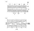
図6は、図1に示した分散補償素子10Xが正負の分散補償を実現するためのものであるのに対し、複数次の項に対する分散補償を実現するためのものである。
ここで、分散補償素子(分散補償部)10Yは、基本的に図1に示した分散補償素子10Xと同様であるため、共通する構成については同符号を付してその説明を省略するが、フォトニック結晶部20は、基板21上に、クラッド層22と、コア層23とが積層されたものである。
このフォトニック結晶部20のコア層23に、周期的に形成された孔24の半径rと間隔aとが、領域ごとに異なるように設定されているのである。FIG. 6 is for realizing dispersion compensation for a plurality of terms, whereas the
Here, since the dispersion compensation element (dispersion compensation unit) 10Y is basically the same as the
The radius r and the interval a of the
複数次の分散補償に対応する分散補償素子10Yは、n次までの項の分散補償を実現するのであれば、2(n−1)個の領域を有している。
図6に示すように、例えば3次までの項の分散補償を行うのであれば、n=3であり、領域は2(n−1)=2(3−1)=4個が設定される。これら4個の領域(I)、(II)、(III)、(IV)において、2次の項の正負、3次の項の正負、計4通りの波長分散を与えるよう、それぞれ孔24の半径rと間隔aが設定されている。The
As shown in FIG. 6, for example, if dispersion compensation of terms up to the third order is performed, n = 3 and 2 (n-1) = 2 (3-1) = 4 regions are set. . In these four regions (I), (II), (III), and (IV), the positive and negative of the second-order term, the positive and negative of the third-order term, and a total of four chromatic dispersions, respectively, are provided. A radius r and an interval a are set.
図7は、このような3次までの項の分散補償を行う場合を説明するためのものである。
この図7に示すように、領域(IV)が2次の項の正、領域(I)が2次の項の負、領域(III)が3次の項の正、領域(II)が3次の項の負の波長分散を与える場合、
領域(IV)では、k=−c2ν2、
領域(I)では、k=c’ 2ν2、
領域(III)では、k=−c’’ 2ν2−c3ν3、
領域(II)では、k=c’’’ 2ν2+c’ 3ν3、
の式で表される曲線となる。ただし、各式は中心周波数付近の周波数−波数特性曲線をνのべき乗で近似して表している。FIG. 7 is a diagram for explaining a case where dispersion compensation of such terms up to the third order is performed.
As shown in FIG. 7, the region (IV) is positive of the second order term, the region (I) is negative of the second order term, the region (III) is positive of the third order term, and the region (II) is 3 Given the negative chromatic dispersion of
In region (IV), k = −c2 ν2 ,
In region (I), k = c ′2 ν2 ,
In region (III), k = −c ″2 ν2 -c3 ν3 ,
In region (II), k = c ′ ″2 ν2 + c ′3 ν3 ,
It becomes a curve expressed by the following formula. However, each expression represents a frequency-wave number characteristic curve near the center frequency approximated by a power of ν.
ここで、k:波数、c:正の数、ν:中心周波数を原点として表した周波数である。
そして、領域(I)〜(IV)をトータルした、
k=(c’ 2−c2+c’’’ 2−c’’ 2)ν2+(c’ 3−c3)ν3
の式において、2次の項の係数:(c’ 2−c2+c’’’ 2−c’’ 2)が分散補償素子10Yにおける2次の分散補償値を与え、3次の項の係数:(c’ 3−c3)が分散補償素子10Yにおける3次の分散補償値を与える。Here, k is the wave number, c is a positive number, and ν is the frequency expressed with the center frequency as the origin.
Then, the regions (I) to (IV) are totaled,
k = (c ′2 −c2 + c ′ ″2 −c ″2 ) ν2 + (c ′3 −c3 ) ν3
Where the coefficient of the second order term: (c ′2 −c2 + c ′ ″2 −c ″2 ) gives the second order dispersion compensation value in the dispersion compensation element 10Y. : (C ′3 −c3 ) gives a third-order dispersion compensation value in the
ところで、上記のような分散補償素子10Yでは、例えば4つの領域(I)〜(IV)を備える構成となっているが、このように3以上の領域を備える場合、図6(b)に示すように、互いに隣接する領域間の境界部で、屈折率の違いから生じる反射による光減衰が最小となるような配列とするのが好ましい。具体的には、間隔aの大小の順で領域(I)〜(IV)を配列するのが望ましい。 By the way, the
さて、図8は、上記したような分散補償素子10Xあるいは10Yを用いて構成する分散補償システム50の構成を示すものである。
分散補償システム50は、光ファイバ伝送路100上に備えられる。
光ファイバ伝送路100は、例えば海底等に長距離にわたって敷設されるもので、送信サーバ等の入射部101側から入射された光パルス列が、光ファイバ伝送路100を介して伝送され、受信サーバ等の出射部102側から出射されるようになっている。FIG. 8 shows a configuration of a
The
The optical
分散補償システム50は、出射部102の近傍に備えられるもので、カプラ(パルス取り出し部)51と、モニター装置52と、制御装置(制御部、電圧制御部)53と、分散補償素子10Xあるいは10Y(以下、単に10Xと略称する)と、を備える。
カプラ51は、光ファイバ伝送路100から光パルスを取り出すものである。
モニター装置52は、カプラ51で取り出した光パルスを、波長分散の影響が無視できるなるべく短尺の光ファイバ54を介して受け取り、その光パルスの波形をモニターする。具体的には、光ファイバ伝送路100から取り出した光パルスの時間−スペクトル面上での波形をモニター(測定)し、波形制御の対象となる光パルスの持つ波長分散を次数毎の係数に分解して求め、これを波長分散情報として出力する。なお、このモニター装置52については、例えば、K Ogawa、“Real−time intuitive spectrogram measurement of ultrashort optical pulses using two−photon absorption in a semiconductor”、[online]、平成14年(2002年)年3月11日、Optics Express、Vol.10,No.5,p.262−267、Optical Society of America、[平成15年(2003年1月14日検索]、インターネット<URL:http://www.opticsexpress.org/abstract.cfm?URI=OPEX−10−5−262>に記載された構成を適用できるので、ここでは特に詳細な説明を行わない。The
The
The
制御装置53は、モニター装置52から出力された波長分散情報を、短尺の光ファイバ55を介して受け取る。この制御装置53は、データベース(データ格納部)56を備えており、このデータベース56には、波長分散の符号と絶対値に応じた、分散補償素子10Xの電極30A、30Bでの電圧印加量のデータが格納されている。
制御装置53では、モニター装置52から出力された波長分散情報を受け取ると、データベース56を参照することで、モニター装置52から受け取った波長分散情報(波長分散の係数)とは絶対値が等しく符号が反転した波長分散を分散補償素子10Xが発生するための、電極30A、30Bでの電圧印加量のデータを得る。そして、得られた電圧印加量のデータを、分散補償素子10Xに向けて出力する。The control device 53 receives the chromatic dispersion information output from the
When the control device 53 receives the chromatic dispersion information output from the
ところで、分散補償素子10Xは、その欠陥導波路25が、光ファイバ伝送路100上に介在し、光ファイバ伝送路100を伝播してきた光パルスが欠陥導波路25の一端側の入射端から入射し、他端側の出射端から光ファイバ伝送路100に出射するように設けられている。
そして、分散補償素子10Xの電極30A、30Bに電圧を印加するための電源(図示無し)と、電源での電圧印加量をコントロールするコントローラ(図示無し)とが、分散補償素子10Xに接続されている。
前記の、制御装置53から出力された電圧印加量のデータは、光ファイバ57を介し、分散補償素子10Xのコントローラ(図示無し)に転送される。コントローラでは、受け取った電圧印加量のデータに基づき、電極30A、30Bに電源から所定の電圧を印加させることで、領域(I)、(II)それぞれの屈折率を変化させる。By the way, in the
A power supply (not shown) for applying a voltage to the
The voltage application amount data output from the control device 53 is transferred via the
このようにして、分散補償システム50では、光ファイバ伝送路100から取り出した光パルスをモニター装置52でモニタリングし、その波長分散情報に基づき、分散補償素子10Xで印加する電圧印加量を制御装置53にてコントロールする構成とした。これにより、光ファイバ伝送路100において、温度、気象等による条件変動が生じても、常に最適な分散補償を行うことができる。
そして、分散補償素子10Xでは、波長分散補償の符号を波長分散の絶対値と独立に可変とすることで、正負の分散補償が行える構成となっているので、光ファイバ伝送路100における波長分散が、正負の間を絶え間なく変化する場合であっても、分散補償を行うことができる。In this way, in the
The
なお、上記の議論は分散補償素子10Xだけでなく分散補償素子10Yを用いた場合にも同様に適用されるものであり、分散補償素子10Yを採用すれば、正負だけでなく、複数次の分散補償を行える。
その結果、分散補償素子10X、10Y、およびそれを用いた分散補償システム50を用いることで、広いスペクトル帯域を利用する超高速大容量光通信に対応する波長分散補償を実現することができ、伝送速度のさらなる高速化を十分に実現することが可能となる。
特に、分散補償素子10X、10Yは、領域毎に孔24の半径rと間隔aを異ならせるのみであるため、特に複雑な構造となることもなく、比較的低コストで上記効果を実現することが可能である。The above discussion applies to the case where not only the
As a result, by using the
In particular, the
また、制御装置53でも、予めデータベース56に格納された情報を参照することで、電極30A、30Bで印加する電圧量を制御する構成となっており、その場で複雑な処理等を行う必要がないため、制御装置53自体も低コストで製作することができる。
さて、上記分散補償素子10Xあるいは10Yは、電極30を用いてバイアス電圧をかけることでフォトニック結晶部20の屈折率を変化させる構成としたが、コア層23に不純物であるキャリア(電子あるいは正孔(ホール))を注入し、バイアス電圧をかけることによってフォトニック結晶部20の吸収スペクトル(屈折率の虚部)を変化させることもできる。The control device 53 is also configured to control the amount of voltage applied by the
The
図9は、そのような分散補償素子10Zの例である。
この図9に示すように、分散補償素子10Zは、全体として、基板21上に、クラッド層22、コア層23が積層され、さらにコア層23上にはクラッド層60が積層された構成を有している。基板21は例えばシリコン(Si)、クラッド層22、60はシリコン酸化膜(SiO2)または窒化シリコン膜、コア層23は誘電体であるシリコン結晶(Si)で形成されている。また、基板21は、例えば500μm程度の厚さを有し、クラッド層22および60は、例えば200nm〜1μm、具体例としては300nm、コア層23は250nm程度の厚さを有している。FIG. 9 shows an example of such a
As shown in FIG. 9, the
分散補償素子10Zは、欠陥導波路25が連続する方向に対して直交した断面、つまり図9に示した断面において、基板21、クラッド層22、コア層23、クラッド層60が、孔24が形成された領域(以下、これをフォトニック結晶領域と称する)R1よりも側方に延長するように形成されている。つまり、欠陥導波路25を中心として、その両側に孔24が形成されたフォトニック結晶領域R1が存在し、さらにその外側に、孔24が形成されていない拡張領域R2が形成されているのである。
上下をクラッド層22および60によって挟み込まれたコア層23には、拡張領域R2に、中央部の欠陥導波路25に対しキャリア密度が異なる領域(異密度領域)が、端子部70として形成されている。In the
In the
そして、このような分散補償素子10Zでは、この端子部70に、電圧を印加するための電極(分散変動手段、エネルギー付与部材)80が電気的に接続され、基板21の底面側には、基準電位を供給するための基準電極81が電気的に接続されている。
端子部70は、コア層23に含まれる不純物(電子または正孔)をドープまたはアンドープすることによって、キャリア密度を欠陥導波路25に対して異ならせたものである。この端子部70に電極80を電気的に接続し、バイアス電圧を印加すると、欠陥導波路25の部分と端子部70の部分のキャリア密度の差により電子または正孔が移動し、これによって欠陥導波路25の部分のキャリア密度が変化し、吸収スペクトルが変化する。例えば、不純物としてp型元素を用いる場合、+(プラス)のバイアス電圧を印加すると、正孔が両側の端子部70から中央部の欠陥導波路25に集まって欠陥導波路25のキャリア密度が上昇し、−(マイナス)のバイアス電圧を印加すると、正孔が欠陥導波路25から両側の端子部70に移動して欠陥導波路25のキャリア密度が低下する。In such a dispersion compensation element 10 </ b> Z, an electrode (dispersion varying means, energy applying member) 80 for applying a voltage is electrically connected to the
The
ここで、欠陥導波路25の部分に対し、端子部70のキャリア密度を低くしてもよいが、欠陥導波路25の部分に対し、端子部70のキャリア密度を高くする、つまり不純物をイオン注入等によってドープするのが好ましい。欠陥導波路25の部分に対し、端子部70のキャリア密度を高くすると、電極80が接続される端子部70では電気抵抗が小さくなり、しかも欠陥導波路25の部分の電気抵抗が大きくなって電界が集中しやすくなるからである。 Here, the carrier density of the
このような不純物としては、半導体でも用いられている、p型元素のB(ホウ素)、Al(アルミニウム)、Ga(ガリウム)、In(インジウム)、Tl(タリウム)、n型元素のN(窒素)、P(リン)、As(砒素)、Sb(アンチモン)、Bi(ビスマス)等がある。これらのうち、p型元素では、ドープを容易に行えることから、B(ホウ素)が特に好適である。
ドープする不純物として、p型元素のB(ホウ素)を用いる場合、例えば、欠陥導波路25のキャリア密度(不純物元素の数)を1017個/cm3とすると、端子部70のキャリア密度を5×1018〜5×1019個/cm3、例えば1×1019個/cm3とするのが好ましい。Examples of such impurities include p-type elements B (boron), Al (aluminum), Ga (gallium), In (indium), Tl (thallium), and n-type elements N (nitrogen), which are also used in semiconductors. ), P (phosphorus), As (arsenic), Sb (antimony), Bi (bismuth), and the like. Among these, B (boron) is particularly suitable for the p-type element because it can be easily doped.
When the p-type element B (boron) is used as the impurity to be doped, for example, when the carrier density (number of impurity elements) of the
この場合、基板21は、キャリア密度を欠陥導波路25と同等とするのが好ましい。基板21と欠陥導波路25とで、キャリア密度が異なると、これらの間に電荷分布が生じてしまい、設計等が複雑になるからである。
また、基板21に基準電極81が接続される面21aにも、電気抵抗を小さくするため、不純物をドープし、例えば端子部70と同等のキャリア密度とするのが好ましい。In this case, the
Also, the
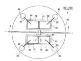
図10は、図9に示したような断面構造を有する分散補償素子10Zの一例である。
この図10に示すように、分散補償素子10Z1は、マウント90上に搭載されており、フォトニック結晶領域R1の面積に対し、その両側の拡張領域R2に形成された端子部70の面積が相対的に大きくなるように形成されて、平面視した状態で略H字状を有している。これは、端子部70の面積をなるべく大きくして、その電気抵抗を小さくするためである。FIG. 10 is an example of a
As shown in FIG. 10, the
また、この分散補償素子10Z1は、図1に示した分散補償素子10Xと同様、孔24の半径rと、間隔aとが異なって設定された領域(I)、(II)を有している。そして、それぞれの領域(I)、(II)に独立してバイアス電圧を印加するため、分散補償素子10Z1は、領域(I)、(II)の両側にそれぞれ端子部70および電極80が設けられ、合計4つの電極80のそれぞれに、リード85を介し、マウント90上に設けられた外部電極86が電気的に接続されている。
そして、フォトニック結晶領域R1の欠陥導波路25の両端に対向するように先球型の光ファイバFが配置され、これによって欠陥導波路25に光パルスが導かれ、分散補償を受けた後に導出されるようになっている。Further, the
Then, a front-end type optical fiber F is arranged so as to face both ends of the
また、図11は、図9に示したような断面構造を有する分散補償素子10Zの他の一例である。
この図11に示すように、分散補償素子10Z2は、フォトニック結晶領域R1に対し、その両側に広がる拡張領域R2に設けられた端子部70および電極80が、台形状(あるいは扇形状)とされたものである。これにより、端子部70および電極80に比較して面積が小さいフォトニック結晶領域R1までの距離をなるべく短くしつつ、端子部70および電極80の面積を大きく確保することができる。これも、端子部70の電気抵抗を小さくするために有効である。FIG. 11 shows another example of the
As shown in FIG. 11, the
図12は、図9に示したような断面構造を有する分散補償素子10Zのさらに他の一例である。
この図12に示すように、分散補償素子10Z3は、その表面のみが、図10に示した分散補償素子10Z1と同様に略H字状とされ、フォトニック結晶領域R1に対し、その両側に広がる端子部70および電極80の面積が大きくなるように形成されている。そして、基板21は、上部のみが平面視略H字状とされ、それより下方の部分は平面視略矩形状をなしている。
このような分散補償素子10Z3は、基板21上に、クラッド層22、コア層23、クラッド層60を積層して平面視矩形状のブロックを形成した後、フォトニック結晶領域R1の欠陥導波路25の両端側をエッチング等により除去して段部91を形成することで得られる。このとき、フォトニック結晶領域R1の欠陥導波路25の両端には、突出部92を形成し、この突出部92に、光ファイバFを対向させる。このため、段部91の深さは、光ファイバFの外径に応じて設定するのが好ましい。FIG. 12 shows still another example of the
As shown in FIG. 12, the
Such
ところで、図10〜図12で示した分散補償素子10Z1〜10Z3は、孔24の半径rと、間隔aとが異なって設定された2つの領域(I)、(II)を有する構成としたが、これを図6に示した分散補償素子10Y等と同様、例えば4つ等、3以上の領域を備えるようにしても良い。その場合、領域の数に応じ、端子部70を設ける。
このような分散補償素子10Zにおいても、図8に示した分散補償システム50を構成することができる。By the way, the
Also in such a
この場合、制御装置53は、データベース56に、波長分散の符号と絶対値に応じた、分散補償素子10Zに対する電極80での電圧印加量のデータが格納されている。そして、制御装置53では、データベース56を参照することで、モニター装置52から受け取った波長分散情報に応じた、電極80での電圧印加量のデータを得て、これを分散補償素子10Zに向けて出力する。
制御装置53から出力された電圧印加量のデータは、光ファイバ57を介し、分散補償素子10Zのコントローラ(図示無し)に転送される。コントローラは、受け取った電圧印加量のデータに基づき電源から所定の電圧を発し、これを電極80を介して端子部70に印加させることで、欠陥導波路25の領域(I)、(II)それぞれの屈折率を変化させる。In this case, the control device 53 stores, in the
The voltage application amount data output from the control device 53 is transferred via the
このようにして、分散補償素子10Zの場合も、分散補償システム50により、光ファイバ伝送路100において、温度、気象等による条件変動が生じても、常に最適な分散補償を行うことができる。その結果、広いスペクトル帯域を利用する超高速大容量光通信に対応する波長分散補償を実現することができ、伝送速度のさらなる高速化を十分に実現することが可能となるのである。 In this way, even in the case of the
なお、上記実施の形態では、分散補償素子10X、10Y、10Zにおいて電極30を用いてバイアス電圧をかけることでフォトニック結晶部20の屈折率を変化させる構成としたが、これ以外の手段を分散補償手段として用いることも可能である。
例えば、各領域にヒータを設け、ヒータに電流を流してコア層23の温度を上昇させるのである。屈折率の温度依存性により、フォトニック結晶導波路の波長分散を変化させて波長分散補償に利用することができる。
さらに、圧電素子によりストレスをフォトニック結晶部20の両面から印加することでひずみを加え、屈折率を変化させることもできる。In the above-described embodiment, the
For example, a heater is provided in each region, and a current is supplied to the heater to raise the temperature of the
Furthermore, the refractive index can be changed by applying strain from both sides of the
また、フォトニック結晶部20は、図13(a)に示すように、基板21上にクラッド層22、コア層23のみを備え、コア層23の一面側には空気が接する構成としたが、これに代えて、図13(b)に示すように、コア層23の上面側にさらにクラッド層(他の層)26を設けるようにしても良い。この場合、クラッド層26には、クラッド層22と同様、SiO2を用いることができる。好ましい態様としてのクラッド層22の厚さは500nmである。その他の部分の厚さ等は前記したのと同様である。
また、コア層23には、直線状の欠陥導波路25を形成する構成としたが、直線状に限るものではなく、折曲あるいは湾曲した形状とすることもできる。さらに、上記実施の形態では、欠陥導波路25は二次元状に形成された構成となっているが、これを三次元状に形成する構成とすることも可能である。In addition, as shown in FIG. 13A, the
Further, the
この他、上記と同様の光に対する分散機能を有するのであれば、フォトニック結晶以外の光学素材、光学素子を用いることに何ら問題はない。
加えて、分散補償システム50では、モニター装置52、制御装置53で光パルスをモニタリングして分散補償を制御する構成としたが、光ファイバ伝送路100における光パルス伝播条件がさほど変動しないような使用環境であれば、カプラ51、モニター装置52、制御装置53を省略し、常に一定の分散補償を行う構成とすることも可能である。In addition, there is no problem in using an optical material or an optical element other than the photonic crystal as long as it has a light dispersion function similar to the above.
In addition, although the
なお、入射部101、出射部102で用いられるサーバや各種端末等は、光ファイバ伝送路100に対し信号の送出と受信の双方を行うのが通常である。上記分散補償システム50は、信号の受信の直前で分散補償を行うのが好ましいため、実際には、光ファイバ伝送路100の両端部に分散補償システム50を備えるのが好ましい。
加えて、分散補償システム50は、モニター装置52、制御装置53と、分散補償素子10X、10Yまたは10Zとを一体の装置としても良いし、それぞれを別体のユニットとしても良い。
これ以外にも、本発明の主旨を逸脱しない限り、上記実施の形態で挙げた構成を取捨選択したり、他の構成に適宜変更することが可能である。In general, servers and various terminals used in the
In addition, in the
In addition to this, as long as it does not depart from the gist of the present invention, the configuration described in the above embodiment can be selected or changed to another configuration as appropriate.
10X,10Y,10Z,10Z1,10Z2,10Z3・・・分散補償素子(分散補償部)、20・・・フォトニック結晶部、21・・・基板、22・・・クラッド層(他の層)、23・・・コア層(周期配列層)、24・・・孔、25・・・欠陥導波路、26・・・クラッド層(他の層)、30・・・電極(分散変動手段、エネルギー付与部材)、50・・・分散補償システム、51・・・カプラ(パルス取り出し部)、52・・・モニター装置、53・・・制御装置(制御部、電圧制御部)、54,55・・・光ファイバ、56・・・データベース、60・・・クラッド層、・・・、70・・・端子部、80・・・電極(分散変動手段、エネルギー付与部材)、81・・・基準電極、85・・・リード、86・・・外部電極、90・・・マウント、91・・・段部、92・・・突出部、100・・・光ファイバ伝送路、100X・・・分散補償素子、101・・・入射部、102・・・出射部。10X, 10Y, 10Z, 10Z1 , 10Z2 , 10Z3 ... dispersion compensation element (dispersion compensation part), 20 ... photonic crystal part, 21 ... substrate, 22 ... cladding layer (others Layer), 23 ... core layer (periodic array layer), 24 ... hole, 25 ... defect waveguide, 26 ... cladding layer (other layers), 30 ... electrode (dispersion variation means) , Energy applying member), 50... Dispersion compensation system, 51... Coupler (pulse extraction unit), 52... Monitor device, 53... Control device (control unit, voltage control unit), 54 and 55. ... Optical fiber, 56 ... Database, 60 ... Cladding layer, ..., 70 ... Terminal part, 80 ... Electrode (dispersion variation means, energy application member), 81 ... Reference Electrode, 85 ... lead, 86 ... external electrode, 90 · Mount, 91 ... stepped portion, 92 ... projecting portion, 100 ... optical fiber transmission line, 100X ... dispersion compensation element, 101 ... incident portion, 102 ... exit portion.
Claims (8)
Translated fromJapanese前記周期配列層は、一方の前記物質中に周期的に配列される他方の前記物質が連続して欠落した連続欠落部が形成されるとともに、
前記連続欠落部が連続する方向において、一方の前記物質中における他方の前記物質の周期配列特性が異なる複数の領域が形成されていることを特徴とする光学結晶。Including a periodic arrangement layer formed by alternately and periodically arranging two substances having different dielectric constants,
The periodic arrangement layer is formed with a continuous missing portion in which the other substance periodically arranged in one of the substances is continuously missing,
An optical crystal, wherein a plurality of regions having different periodic arrangement characteristics of the other substance in one of the substances are formed in a direction in which the continuous missing portions are continuous.
The optical crystal according to claim 6, wherein the different density region has a larger area than the plurality of regions.
Priority Applications (1)
| Application Number | Priority Date | Filing Date | Title |
|---|---|---|---|
| JP2010051141AJP2010164989A (en) | 2003-01-15 | 2010-03-08 | Optical crystal |
Applications Claiming Priority (2)
| Application Number | Priority Date | Filing Date | Title |
|---|---|---|---|
| JP2003007485 | 2003-01-15 | ||
| JP2010051141AJP2010164989A (en) | 2003-01-15 | 2010-03-08 | Optical crystal |
Related Parent Applications (1)
| Application Number | Title | Priority Date | Filing Date |
|---|---|---|---|
| JP2005507997ADivisionJP4668065B2 (en) | 2003-01-15 | 2004-01-14 | Dispersion compensation element, dispersion compensation system, dispersion compensation method |
Publications (1)
| Publication Number | Publication Date |
|---|---|
| JP2010164989Atrue JP2010164989A (en) | 2010-07-29 |
Family
ID=32709117
Family Applications (2)
| Application Number | Title | Priority Date | Filing Date |
|---|---|---|---|
| JP2005507997AExpired - Fee RelatedJP4668065B2 (en) | 2003-01-15 | 2004-01-14 | Dispersion compensation element, dispersion compensation system, dispersion compensation method |
| JP2010051141APendingJP2010164989A (en) | 2003-01-15 | 2010-03-08 | Optical crystal |
Family Applications Before (1)
| Application Number | Title | Priority Date | Filing Date |
|---|---|---|---|
| JP2005507997AExpired - Fee RelatedJP4668065B2 (en) | 2003-01-15 | 2004-01-14 | Dispersion compensation element, dispersion compensation system, dispersion compensation method |
Country Status (5)
| Country | Link |
|---|---|
| US (1) | US7515785B2 (en) |
| EP (2) | EP1584969A4 (en) |
| JP (2) | JP4668065B2 (en) |
| CN (1) | CN100363784C (en) |
| WO (1) | WO2004063797A1 (en) |
Families Citing this family (11)
| Publication number | Priority date | Publication date | Assignee | Title |
|---|---|---|---|---|
| JP2006276576A (en)* | 2005-03-30 | 2006-10-12 | Ricoh Co Ltd | Light control element and light control element manufacturing method |
| JP4549949B2 (en)* | 2005-08-12 | 2010-09-22 | 株式会社フジクラ | Optical element |
| US8374469B2 (en) | 2006-02-09 | 2013-02-12 | Nec Corporation | Optical waveguide |
| JP4936313B2 (en)* | 2006-08-25 | 2012-05-23 | 日本碍子株式会社 | Light modulation element |
| EP2761248B8 (en)* | 2011-09-26 | 2017-07-12 | WaveLight GmbH | Optical coherence tomography technique |
| US10718901B2 (en) | 2013-06-26 | 2020-07-21 | Micron Technology, Inc. | Photonic device having a photonic crystal lower cladding layer provided on a semiconductor substrate |
| US10386581B2 (en) | 2013-10-25 | 2019-08-20 | Forelux Inc. | Grating based optical transmitter |
| US9671673B2 (en)* | 2014-11-17 | 2017-06-06 | Singapore University Of Technology And Design | Optical device for dispersion compensation |
| CN110301075B (en)* | 2016-07-05 | 2021-05-07 | 光引研创股份有限公司 | Grating Based Optical Transmitter |
| CN111157491B (en)* | 2020-01-10 | 2021-09-14 | 燕山大学 | Array sensing structure with photonic crystal microcavity and optical waveguide laterally coupled |
| US20230084066A1 (en)* | 2021-09-14 | 2023-03-16 | Huawei Technologies Co., Ltd. | System and method for dispersion compensation in fibered optical communication paths |
Citations (2)
| Publication number | Priority date | Publication date | Assignee | Title |
|---|---|---|---|---|
| JP2002303836A (en)* | 2001-04-04 | 2002-10-18 | Nec Corp | Optical switch with photonic crystal structure |
| JP2003279764A (en)* | 2002-03-26 | 2003-10-02 | Japan Science & Technology Corp | Two-dimensional photonic crystal optical multiplexer / demultiplexer |
Family Cites Families (14)
| Publication number | Priority date | Publication date | Assignee | Title |
|---|---|---|---|---|
| JPH06216467A (en)* | 1993-01-19 | 1994-08-05 | Hitachi Ltd | Semiconductor optical dispersion compensator |
| JP3146089B2 (en)* | 1993-04-20 | 2001-03-12 | 三菱電機株式会社 | Dispersion compensation optical amplifier repeater |
| JP2000121987A (en) | 1998-10-20 | 2000-04-28 | Nec Corp | Wavelength dispersion compensator |
| US6289151B1 (en) | 1998-10-30 | 2001-09-11 | Lucent Technologies Inc. | All-pass optical filters |
| DE19915139A1 (en)* | 1999-03-26 | 2000-09-28 | Deutsche Telekom Ag | Method for dispersion compensation of commonly transmitted optical signals with different wavelengths |
| CA2324709A1 (en) | 1999-11-05 | 2001-05-05 | Jds Uniphase Inc. | Tunable dispersion compensator |
| US6768822B1 (en)* | 2000-04-28 | 2004-07-27 | Nortel Networks Limited | Chromatic dispersion compensation |
| DE10024884A1 (en)* | 2000-05-19 | 2001-11-22 | Bosch Gmbh Robert | Gear pump |
| US6674949B2 (en) | 2000-08-15 | 2004-01-06 | Corning Incorporated | Active photonic crystal waveguide device and method |
| JP3879411B2 (en)* | 2001-02-14 | 2007-02-14 | 日本電気株式会社 | Dispersion compensator |
| US20020159672A1 (en)* | 2001-03-13 | 2002-10-31 | Fells Julian A. | Adjustable dispersion compensators, adjustable optical filters, and control signals and strain applicators therefor |
| JP3665273B2 (en)* | 2001-05-11 | 2005-06-29 | 株式会社日立製作所 | Chromatic dispersion compensator and optical transmission system using the same |
| EP1278082A1 (en)* | 2001-07-17 | 2003-01-22 | Alcatel | A chromatic dispersion compensator |
| JP4028751B2 (en)* | 2002-04-24 | 2007-12-26 | 株式会社日立製作所 | Optical waveguide and optical element using the same |
- 2004
- 2004-01-14JPJP2005507997Apatent/JP4668065B2/ennot_activeExpired - Fee Related
- 2004-01-14WOPCT/JP2004/000170patent/WO2004063797A1/enactiveApplication Filing
- 2004-01-14CNCNB2004800014704Apatent/CN100363784C/ennot_activeExpired - Fee Related
- 2004-01-14USUS10/542,383patent/US7515785B2/ennot_activeExpired - Fee Related
- 2004-01-14EPEP04702048Apatent/EP1584969A4/ennot_activeWithdrawn
- 2004-01-14EPEP10183405Apatent/EP2267515A3/ennot_activeWithdrawn
- 2010
- 2010-03-08JPJP2010051141Apatent/JP2010164989A/enactivePending
Patent Citations (2)
| Publication number | Priority date | Publication date | Assignee | Title |
|---|---|---|---|---|
| JP2002303836A (en)* | 2001-04-04 | 2002-10-18 | Nec Corp | Optical switch with photonic crystal structure |
| JP2003279764A (en)* | 2002-03-26 | 2003-10-02 | Japan Science & Technology Corp | Two-dimensional photonic crystal optical multiplexer / demultiplexer |
Non-Patent Citations (1)
| Title |
|---|
| JPN6012053492; '2次元フォトニック結晶による波長分合波デバイス-面内ヘテロ構造の提案-' 第49回応用物理学関係連合講演会講演予稿集 No.3,29p-L-9, 200203, 1039* |
Also Published As
| Publication number | Publication date |
|---|---|
| US20060051016A1 (en) | 2006-03-09 |
| JP4668065B2 (en) | 2011-04-13 |
| CN100363784C (en) | 2008-01-23 |
| US7515785B2 (en) | 2009-04-07 |
| EP1584969A4 (en) | 2008-07-23 |
| EP2267515A3 (en) | 2012-12-12 |
| EP2267515A2 (en) | 2010-12-29 |
| EP1584969A1 (en) | 2005-10-12 |
| WO2004063797A1 (en) | 2004-07-29 |
| JPWO2004063797A1 (en) | 2006-05-18 |
| CN1717612A (en) | 2006-01-04 |
Similar Documents
| Publication | Publication Date | Title |
|---|---|---|
| JP2010164989A (en) | Optical crystal | |
| JP3917170B2 (en) | Dispersion compensation element | |
| JP5455955B2 (en) | Ring light modulator | |
| CN104885003B (en) | Optical waveguide components and optical modulator | |
| JP4936313B2 (en) | Light modulation element | |
| US20160290891A1 (en) | Wafer level testing of optical devices | |
| US20090245714A1 (en) | Optical Resonator Tuning Using Piezoelectric Actuation | |
| FR2756938A1 (en) | DEVICE, IN PARTICULAR A SEMICONDUCTOR, FOR THE TREATMENT OF TWO WAVES, IN PARTICULAR LUMINOUS | |
| US20160246020A1 (en) | Optical Coupler Provided With an Intermediate Waveguide | |
| FR2694819A1 (en) | Speed adaptation device between electrical and optical signals. | |
| CN100407378C (en) | Polycrystalline germanium-based waveguide detector integrated on epitaxial silicon thin plate on insulating substrate | |
| US11048046B2 (en) | Optical coupler provided with a structuration | |
| JP3014039B2 (en) | Optical pulse dispersion compensator, optical pulse compressor using the same, semiconductor short pulse laser device, and optical communication system | |
| Xu et al. | Enhanced photo response at two-micron-wavelength using GeSn/Ge multiple-quantum-well waveguide | |
| US9568671B2 (en) | Nanotube electro-optical component, optronic or optical link-based hybrid integrated circuit integrating this component, and method of fabrication | |
| JP3957190B2 (en) | Variable optical attenuator | |
| Chu et al. | Compact, low power consumption wavelength tunable laser with silicon photonic-wire waveguide micro-ring resonators | |
| JP2006351917A (en) | Optical integrated circuit | |
| JP2009205089A (en) | Optical element, wavelength dispersion correcting element, and phase modulation element | |
| JP5658895B2 (en) | Optical element | |
| Verdier | Design, Modeling, Fabrication, Characterization and Applications of very Wideband Semiconductor Optical Amplifiers | |
| JPS6237826B2 (en) | ||
| JP2013050676A (en) | Positioning method of optical device | |
| EP1232550A1 (en) | Semiconductor optical amplifier | |
| CN1860390A (en) | Opto-Gap Chambers for Waveguide Configurations |
Legal Events
| Date | Code | Title | Description |
|---|---|---|---|
| A131 | Notification of reasons for refusal | Free format text:JAPANESE INTERMEDIATE CODE: A131 Effective date:20121016 | |
| A02 | Decision of refusal | Free format text:JAPANESE INTERMEDIATE CODE: A02 Effective date:20130521 |