JP2010162796A - Surface material for stamper - Google Patents
Surface material for stamperDownload PDFInfo
- Publication number
- JP2010162796A JP2010162796AJP2009007926AJP2009007926AJP2010162796AJP 2010162796 AJP2010162796 AJP 2010162796AJP 2009007926 AJP2009007926 AJP 2009007926AJP 2009007926 AJP2009007926 AJP 2009007926AJP 2010162796 AJP2010162796 AJP 2010162796A
- Authority
- JP
- Japan
- Prior art keywords
- diamond
- carbon
- stamper
- surface material
- layer
- Prior art date
- Legal status (The legal status is an assumption and is not a legal conclusion. Google has not performed a legal analysis and makes no representation as to the accuracy of the status listed.)
- Granted
Links
- 239000000463materialSubstances0.000titleclaimsabstractdescription34
- 229910003460diamondInorganic materials0.000claimsabstractdescription100
- 239000010432diamondSubstances0.000claimsabstractdescription100
- OKTJSMMVPCPJKN-UHFFFAOYSA-NCarbonChemical compound[C]OKTJSMMVPCPJKN-UHFFFAOYSA-N0.000claimsabstractdescription44
- 229910052799carbonInorganic materials0.000claimsabstractdescription43
- 239000013078crystalSubstances0.000claimsdescription13
- 229910003481amorphous carbonInorganic materials0.000claimsdescription4
- 239000000203mixtureSubstances0.000claimsdescription4
- 238000000034methodMethods0.000abstractdescription16
- 230000015572biosynthetic processEffects0.000description8
- 230000000694effectsEffects0.000description8
- 238000004519manufacturing processMethods0.000description7
- 238000005229chemical vapour depositionMethods0.000description6
- 239000000853adhesiveSubstances0.000description3
- 230000001070adhesive effectEffects0.000description3
- 238000009751slip formingMethods0.000description3
- KRHYYFGTRYWZRS-UHFFFAOYSA-NFluoraneChemical compoundFKRHYYFGTRYWZRS-UHFFFAOYSA-N0.000description2
- PXHVJJICTQNCMI-UHFFFAOYSA-NNickelChemical compound[Ni]PXHVJJICTQNCMI-UHFFFAOYSA-N0.000description2
- 238000001459lithographyMethods0.000description2
- 239000007769metal materialSubstances0.000description2
- 239000012495reaction gasSubstances0.000description2
- 239000000243solutionSubstances0.000description2
- UFHFLCQGNIYNRP-UHFFFAOYSA-NHydrogenChemical compound[H][H]UFHFLCQGNIYNRP-UHFFFAOYSA-N0.000description1
- GRYLNZFGIOXLOG-UHFFFAOYSA-NNitric acidChemical compoundO[N+]([O-])=OGRYLNZFGIOXLOG-UHFFFAOYSA-N0.000description1
- XUIMIQQOPSSXEZ-UHFFFAOYSA-NSiliconChemical compound[Si]XUIMIQQOPSSXEZ-UHFFFAOYSA-N0.000description1
- RTAQQCXQSZGOHL-UHFFFAOYSA-NTitaniumChemical compound[Ti]RTAQQCXQSZGOHL-UHFFFAOYSA-N0.000description1
- 238000001015X-ray lithographyMethods0.000description1
- 239000000956alloySubstances0.000description1
- 229910045601alloyInorganic materials0.000description1
- 150000001722carbon compoundsChemical class0.000description1
- 238000005336crackingMethods0.000description1
- 238000001312dry etchingMethods0.000description1
- 238000000609electron-beam lithographyMethods0.000description1
- 238000005530etchingMethods0.000description1
- 239000007789gasSubstances0.000description1
- 239000011521glassSubstances0.000description1
- 238000010438heat treatmentMethods0.000description1
- 238000004050hot filament vapor depositionMethods0.000description1
- 229930195733hydrocarbonNatural products0.000description1
- 150000002430hydrocarbonsChemical class0.000description1
- 238000005304joiningMethods0.000description1
- 239000011259mixed solutionSubstances0.000description1
- 229910052759nickelInorganic materials0.000description1
- 229910017604nitric acidInorganic materials0.000description1
- NJPPVKZQTLUDBO-UHFFFAOYSA-NnovaluronChemical compoundC1=C(Cl)C(OC(F)(F)C(OC(F)(F)F)F)=CC=C1NC(=O)NC(=O)C1=C(F)C=CC=C1FNJPPVKZQTLUDBO-UHFFFAOYSA-N0.000description1
- 238000000206photolithographyMethods0.000description1
- 238000005268plasma chemical vapour depositionMethods0.000description1
- 230000002265preventionEffects0.000description1
- 238000000926separation methodMethods0.000description1
- 229910052710siliconInorganic materials0.000description1
- 239000010703siliconSubstances0.000description1
- 239000010935stainless steelSubstances0.000description1
- 229910001220stainless steelInorganic materials0.000description1
- 239000000758substrateSubstances0.000description1
- 229920003002synthetic resinPolymers0.000description1
- 239000000057synthetic resinSubstances0.000description1
- 239000010936titaniumSubstances0.000description1
- 229910052719titaniumInorganic materials0.000description1
- 230000009466transformationEffects0.000description1
Images


Landscapes
- Moulds For Moulding Plastics Or The Like (AREA)
- Shaping Of Tube Ends By Bending Or Straightening (AREA)
- Manufacturing Of Magnetic Record Carriers (AREA)
- Manufacturing Optical Record Carriers (AREA)
Abstract
Translated fromJapaneseDescription
Translated fromJapanese本発明は、ホットプレス法によるナノプリントに使用されるスタンパの型押面に取付けられるスタンパ用表面材に係る技術分野に属する。 The present invention belongs to a technical field related to a stamper surface material attached to a stamping surface of a stamper used for nanoprinting by a hot press method.
最近、ホットプレス法によるナノプリントの対象とされる被加工物が合成樹脂材からガラス材,金属材に拡張され、表面に微細な凹凸パターンが形成され被加工物に圧接されるスタンパ用表面材に相当程度の硬度と耐摩耗性とが要求されるようになってきている。 A stamper surface material that has recently been expanded from a synthetic resin material to a glass material or a metal material, and has a fine concavo-convex pattern formed on the surface and pressed against the workpiece. Therefore, a considerable degree of hardness and wear resistance have been demanded.
従来、硬度,耐摩耗性を高めることを指向したスタンパ用表面材としては、例えば、特許文献1に記載のものが知られている。
特許文献1には、表面に微細な凹凸パターンが形成されたダイヤモンドからなる薄片形のスタンパ用表面材が記載されている。
特許文献1に係るスタンパ用表面材は、材料として硬度,耐摩耗性の高いダイヤモンドを選択することで被加工物への圧接による変形を防止するものである。なお、このスタンパ用表面材は、加熱による変形を防止するために、熱膨張係数がほぼ同一で相対的に厚さのある台座に接合されて型押面に取付けられる構成が採られる。Conventionally, as a stamper surface material aimed at increasing hardness and wear resistance, for example, a material described in Patent Document 1 is known.
Patent Document 1 describes a flaky stamper surface material made of diamond having a fine concavo-convex pattern formed on the surface thereof.
The stamper surface material according to Patent Document 1 prevents deformation due to pressure contact with a workpiece by selecting diamond having high hardness and wear resistance as a material. In addition, in order to prevent the deformation | transformation by heating, the surface material for stampers employ | adopted the structure attached to a stamping surface by joining to the base with substantially the same thermal expansion coefficient and relatively thick.
特許文献1に係るスタンパ用表面材では、薄片形であることからダイヤモンド結晶の生成過程の応力でそりが生じやすく台座に接合されてもそりが消失するわけではないため、被加工物への圧接によって割れが生じやすく、ナノプリントの精度も低くなってしまうという問題点がある。 Since the surface material for a stamper according to Patent Document 1 has a thin piece shape, warpage is likely to occur due to the stress of the diamond crystal formation process, and the warpage does not disappear even if it is joined to the pedestal. However, there is a problem that cracks are easily generated and the accuracy of nanoprinting is lowered.
本発明は、このような問題点を考慮してなされたもので、被加工物への圧接による変形を防止する硬度,耐摩耗性を備えしかもそりが生じることのない薄片形のスタンパ用表面材を提供することを課題とする。 The present invention has been made in consideration of such problems, and has a hardness and wear resistance for preventing deformation due to pressure contact with a workpiece, and is a flaky stamper surface material that does not warp. It is an issue to provide.
前述の課題を解決するため、本発明に係るスタンパ用表面材は、特許請求の範囲の各請求項に記載の手段を採用する。 In order to solve the above-described problems, the stamper surface material according to the present invention employs means described in each of the claims.
即ち、請求項1では、表面に微細な凹凸パターンが形成された薄片形のスタンパ用表面材において、表面がダイヤモンドとされ表面のダイヤモンドの背面側に炭素を主成分とする非ダイヤモンドの層が存在する積層体からなることを特徴とする。 That is, according to claim 1, in the surface material for a flaky stamper having a fine uneven pattern formed on the surface, the surface is a diamond, and a non-diamond layer mainly composed of carbon is present on the back side of the surface diamond. It consists of the laminated body which carries out.
この手段では、微細な凹凸パターンが形成された表面をダイヤモンドとすることで被加工物への圧接による変形を防止する硬度,耐摩耗性を維持し、表面のダイヤモンドの背面側に炭素を主成分とする非ダイヤモンドの層が存在する積層体とすることでダイヤモンド結晶の生成過程の応力の影響を低減する。 With this method, the surface on which the fine unevenness pattern is formed is made of diamond to maintain hardness and wear resistance that prevent deformation due to pressure contact with the work piece, and carbon is the main component on the back side of the surface diamond. The effect of stress on the formation process of diamond crystals is reduced by using a laminate in which a non-diamond layer exists.
また、請求項2では、表面に微細な凹凸パターンが形成された薄片形のスタンパ用表面材において、表面がダイヤモンドとされ表面のダイヤモンドの背面側に炭素を主成分とする非ダイヤモンドの層とダイヤモンドの層とが存在する積層体からなることを特徴とする。 Further, according to
この手段では、微細な凹凸パターンが形成された表面をダイヤモンドとすることで被加工物への圧接による変形を防止する硬度,耐摩耗性を維持し、表面のダイヤモンドの背面側に炭素を主成分とする非ダイヤモンドの層が存在する積層体とすることでダイヤモンド結晶の生成過程の応力の影響を低減する。また、表面のダイヤモンドの背面側にダイヤモンドの層を存在させることで、相対的に硬度,耐摩耗性の低い非ダイヤモンドの層を補完する。 With this method, the surface on which the fine unevenness pattern is formed is made of diamond to maintain hardness and wear resistance that prevent deformation due to pressure contact with the work piece, and carbon is the main component on the back side of the surface diamond. The effect of stress on the formation process of diamond crystals is reduced by using a laminate in which a non-diamond layer exists. In addition, the presence of a diamond layer on the back side of the surface diamond complements the non-diamond layer having relatively low hardness and wear resistance.
また、請求項3では、請求項1または2のスタンパ用表面材において、炭素を主成分とする非ダイヤモンドがダイヤモンドライクカーボン,テトラヘドラル,アモルファスダイヤ等の非晶質炭素からなることを特徴とする。 According to a third aspect of the present invention, in the stamper surface material of the first or second aspect, the non-diamond containing carbon as a main component is made of amorphous carbon such as diamond-like carbon, tetrahedral, amorphous diamond, or the like.
この手段では、炭素を主成分とする非ダイヤモンドがダイヤモンドライクカーボン(DLC)等の非晶質炭素とされることで、ダイヤモンド,非ダイヤモンドが共通性のある製造法によって形成される。 In this means, non-diamond mainly composed of carbon is made amorphous carbon such as diamond-like carbon (DLC), so that diamond and non-diamond are formed by a common manufacturing method.
また、請求項4では、請求項3のスタンパ用表面材において、ダイヤモンドとダイヤモンドライクカーボンとはダイヤモンド結晶の組成勾配をもって連続的に成膜されたものであることを特徴とする。 According to a fourth aspect of the present invention, in the stamper surface material according to the third aspect, the diamond and diamond-like carbon are continuously formed with a composition gradient of diamond crystals.
この手段では、ダイヤモンドとダイヤモンドライクカーボンとがダイヤモンド結晶の組成勾配をもって連続的に成膜されることで、ダイヤモンドと非ダイヤモンドとの間に界面が形成されなくなる。 By this means, diamond and diamond-like carbon are continuously formed with a compositional gradient of diamond crystals, so that no interface is formed between diamond and non-diamond.
本発明に係るスタンパ用表面材は、微細な凹凸パターンが形成された表面をダイヤモンドとすることで被加工物への圧接による変形を防止する硬度,耐摩耗性を維持し、表面のダイヤモンドの背面側に炭素を主成分とする非ダイヤモンドの層が存在する積層体とすることでダイヤモンド結晶の生成過程の応力の影響を非ダイヤモンドの層で低減するため、被加工物への圧接による変形を防止する硬度,耐摩耗性を備えしかもそりが生じることのない薄片形とすることができる効果がある。 The surface material for a stamper according to the present invention maintains hardness and wear resistance to prevent deformation due to pressure contact with a workpiece by making the surface on which a fine concavo-convex pattern is formed a diamond, and the back surface of the surface diamond By forming a laminate with a non-diamond layer mainly composed of carbon on the side, the non-diamond layer reduces the influence of stress on the diamond crystal formation process, preventing deformation due to pressure contact with the workpiece. It has the effect of being able to be made into a flake shape having hardness and wear resistance that does not cause warpage.
さらに、請求項2として、微細な凹凸パターンが形成された表面をダイヤモンドとすることで被加工物への圧接による変形を防止する硬度,耐摩耗性を維持し、表面のダイヤモンドの背面側に炭素を主成分とする非ダイヤモンドの層が存在する積層体とすることでダイヤモンド結晶の生成過程の応力の影響を非ダイヤモンドの層で低減するため、被加工物への圧接による変形を防止する硬度,耐摩耗性を備えしかもそりが生じることのない薄片形とすることができる効果がある。また、表面のダイヤモンドの背面側にもダイヤモンドの層を存在させることで、相対的に硬度,耐摩耗性の低い非ダイヤモンドの層を補完するため、全体の硬度,耐摩耗性が高められ被加工物への圧接による変形がより確実に防止される効果がある。 Further, as claimed in
さらに、請求項3として、炭素を主成分とする非ダイヤモンドがダイヤモンドライクカーボン(DLC)とされることで、ダイヤモンド,非ダイヤモンドが共通性のある製造法によって形成されるため、製造が安価,容易になる効果がある。 Further, as claimed in
さらに、請求項4として、ダイヤモンドとダイヤモンドライクカーボンとがダイヤモンド結晶の組成勾配をもって連続的に成膜されることで、ダイヤモンドとダイヤモンドライクカーボンとの間に界面が形成されなくなるため、ダイヤモンドとダイヤモンドライクカーボンとの剥離が防止される効果がある。 Further, as claimed in claim 4, since diamond and diamond-like carbon are continuously formed with a composition gradient of diamond crystals, an interface is not formed between diamond and diamond-like carbon. There is an effect of preventing separation from carbon.
以下、本発明に係るスタンパ用表面材を実施するための形態を図面に基づいて説明する。 EMBODIMENT OF THE INVENTION Hereinafter, the form for implementing the surface material for stampers concerning this invention is demonstrated based on drawing.
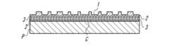
図1,図2は、本発明に係るスタンパ用表面材を実施するための形態の第1例を示すものである。 1 and 2 show a first example of a mode for carrying out a stamper surface material according to the present invention.
第1例は、図1に示すように、表面に微細な凹凸パターン1が形成され薄片形とされた2層の積層体からなるものが接着剤Cで金属材等のバックアッププレートPに貼着されている。凹凸パターン1を含む表面側のある程度の厚さをもった層は、ダイヤモンド2からなる。接着剤Cに対面するダイヤモンド2の背面側の層は、炭素を主成分とする非ダイヤモンドであるダイヤモンドライクカーボン3からなる。 In the first example, as shown in FIG. 1, a two-layer laminate having a fine uneven pattern 1 formed on the surface and formed into a thin piece is adhered to a backup plate P such as a metal material with an adhesive C. Has been. The layer having a certain thickness on the surface side including the uneven pattern 1 is made of
第1例の製造方法については、図2に示されている。 The manufacturing method of the first example is shown in FIG.
まず、図2(A)に示すように、マザーモールドMが製作される。マザーモールドMは、シリコン基板にリソグラフィー技術により前述の凹凸パターン1に対応(凹凸が逆の)した微細な凹凸パターンを形成したものである。即ち、光源としてステッパーを用い、レジストを使用してフォトマスクにより微細な凹凸パターンを感光,現像した後、ドライエッチング(エッチングガスCF4,SF6,CHF3,O2)する。リソグラフィー技術としては、フォトリソグラフィー,電子線リソグラフィー,X線リソグラフィーを選択することができる。First, as shown in FIG. 2A, a mother mold M is manufactured. The mother mold M is obtained by forming a fine concavo-convex pattern corresponding to the above-described concavo-convex pattern 1 (reverse concavo-convex) on a silicon substrate by a lithography technique. That is, a stepper is used as a light source, a fine uneven pattern is exposed and developed with a photomask using a resist, and then dry etching (etching gas CF4 , SF6 , CHF3 , O2 ) is performed. As the lithography technique, photolithography, electron beam lithography, and X-ray lithography can be selected.
次ぎに、図2(B)に示すように、マザーモールドMの微細な凹凸パターンの上に化学的気相成長法(CVD法)によりダイヤモンド2を成膜する。即ち、反応ガス(炭化水素を含み水素ガス等)雰囲気下の高温のチャンバの内部を減圧して、励起された炭素種をマザーモールドMの微細な凹凸パターンに衝突させる。化学的気相成長法としては、マイクロ波CVD法,プラズマCVD法,熱フィラメントCVD法を選択することができる。 Next, as shown in FIG. 2B, a
次ぎに、図2(C)に示すように、ダイヤモンド2の上に化学的気相成長法によりダイヤモンドライクカーボン3を成膜する。ダイヤモンドライクカーボン3は、ダイヤモンド構造(結晶)であるSP3結合のみからなるダイヤモンド2に対して、ダイヤモンド構造であるSP3結合とグラファイト構造であるSP3結合とが混在したアモルファス(非結晶)構造からなる。従って、化学的気相成長法において、反応ガスの濃度や温度,圧力を調整することで、ダイヤモンド2,ダイヤモンドライクカーボン3の成膜の変換が可能である。特に、共通のチャンバの内部でダイヤモンド結晶の組成勾配をもって連続的に成膜されることで、ダイヤモンド2とダイヤモンドライクカーボン3との間に界面が形成されなくなるため、ダイヤモンド2とダイヤモンドライクカーボン3との一体性が得られ剥離が防止される。このダイヤモンドライクカーボン3は、ダイヤモンド2に積層されたことになって、ダイヤモンド2のダイヤモンド結晶の生成過程の応力を低減させる機能を奏する。なお、実装上の要請から、ダイヤモンド2,ダイヤモンドライクカーボン3の成膜の合計厚さとしては0.1mm以上が好ましい。 Next, as shown in FIG. 2C, a diamond-
次ぎに、図2(D),(E)に示すように、ダイヤモンド2,ダイヤモンドライクカーボン3が成膜されたマザーモールドMを容器Bに貯溜された溶解液Wに浸漬させ、マザーモールドMを溶解させる。溶解液Wとしては、例えば、フッ酸・硝酸混合液が使用される。マザーモールドMを溶解させる手段を採ることによって、機械的な剥離手段と採る場合に比して、露出されるダイヤモンド2からなる表面の微細な凹凸パターン1を損傷を避けることができる。 Next, as shown in FIGS. 2D and 2E, the mother mold M on which the
この後、バックアッププレートPに接着剤Cを介してダイヤモンドライクカーボン3側を貼着する。バックアッププレートPとしては、例えば、ステンレス鋼,ニッケル耐熱合金が使用される。接着座Cとしては、例えば、チタン活性ローが使用される。 Thereafter, the diamond-
第1例によると、微細な凹凸パターン1が形成された表面をダイヤモンド2とすることで、被加工物への圧接による変形を防止する硬度,耐摩耗性を維持することができる。また、表面のダイヤモンド2の背面側に炭素を主成分とする非ダイヤモンドであるダイヤモンドライクカーボン3の層が存在する積層体とすることで、ダイヤモンド結晶の生成過程の応力の影響をダイヤモンドライクカーボン3で低減することができるため、薄片形であるにもかかわらずそりが生じることがなくなる。そりの発生の防止は、被加工物への圧接による割れを防止して耐久性能を高めるとともに、ナノプリントの精度を高めることになる。 According to the first example, the surface on which the fine concavo-convex pattern 1 is formed is made of
図3は、本発明に係るスタンパ用表面材を実施するための形態の第2例を示すものである。 FIG. 3 shows a second example of the embodiment for carrying out the stamper surface material according to the present invention.
第2例は、ダイヤモンド2を微細な凹凸パターン1の凹凸に沿った薄性の層としてある。即ち、ダイヤモンド2を第1例のようにな凹凸パターン1を含む表面側のある程度の厚さをもった層としていない。 In the second example, the
第2例によると、製造(成膜)コストの掛かるダイヤモンド2を低減することができる。しかも、微細な凹凸パターン1が形成された表面がダイヤモンド2であることに変わりがないため、被加工物への圧接による変形を防止する硬度,耐摩耗性を維持することができる。 According to the second example, it is possible to reduce
図4は、本発明に係るスタンパ用表面材を実施するための形態の第3例を示すものである。 FIG. 4 shows a third example of the embodiment for carrying out the stamper surface material according to the present invention.
第3例は、第1例のダイヤモンドライクカーボン3の層にダイヤモンド2の層を介在させている。 In the third example, a
第3例によると、表面のダイヤモンド2の背面側にもダイヤモンド2の層を存在させることで、相対的に硬度,耐摩耗性の低いダイヤモンドライクカーボン3の層を補完することができる。このため、全体の硬度,耐摩耗性が高められ被加工物への圧接による変形がより確実に防止されることになる。 According to the third example, the diamond-
第3例については、第2例のダイヤモンドライクカーボン3の層にダイヤモンド2の層を介在させることも可能である。 In the third example, the diamond-
以上、図示した各例の外に、ダイヤモンドライクカーボン3に他の材料を加えることも可能である。 As described above, other materials can be added to the diamond-
さらに、非ダイヤモンドとしてダイヤモンドライクカーボン3に代えてテトラヘドラル,アモルファスダイヤ等の非晶質炭素を選択することも可能である。 Furthermore, it is possible to select amorphous carbon such as tetrahedral or amorphous diamond instead of diamond-
1 微細な凹凸パターン
2 ダイヤモンド
3 ダイヤモンドライクカーボン(非ダイヤモンド)1 Fine
Claims (4)
Translated fromJapanesePriority Applications (1)
| Application Number | Priority Date | Filing Date | Title |
|---|---|---|---|
| JP2009007926AJP5305388B2 (en) | 2009-01-16 | 2009-01-16 | Stamper surface material |
Applications Claiming Priority (1)
| Application Number | Priority Date | Filing Date | Title |
|---|---|---|---|
| JP2009007926AJP5305388B2 (en) | 2009-01-16 | 2009-01-16 | Stamper surface material |
Publications (2)
| Publication Number | Publication Date |
|---|---|
| JP2010162796Atrue JP2010162796A (en) | 2010-07-29 |
| JP5305388B2 JP5305388B2 (en) | 2013-10-02 |
Family
ID=42579381
Family Applications (1)
| Application Number | Title | Priority Date | Filing Date |
|---|---|---|---|
| JP2009007926AExpired - Fee RelatedJP5305388B2 (en) | 2009-01-16 | 2009-01-16 | Stamper surface material |
Country Status (1)
| Country | Link |
|---|---|
| JP (1) | JP5305388B2 (en) |
Citations (5)
| Publication number | Priority date | Publication date | Assignee | Title |
|---|---|---|---|---|
| JPH1096808A (en)* | 1996-09-24 | 1998-04-14 | Nippon Telegr & Teleph Corp <Ntt> | Fine pattern formation method |
| JP2006289684A (en)* | 2005-04-07 | 2006-10-26 | Kobe Steel Ltd | Microprocessing mold |
| JP2007116163A (en)* | 2005-10-18 | 2007-05-10 | Korea Inst Of Machinery & Materials | Stamp for fine imprint lithography and manufacturing method thereof |
| JP2007137066A (en)* | 2005-11-18 | 2007-06-07 | Kofukin Seimitsu Kogyo (Shenzhen) Yugenkoshi | Mold with diamond-like carbon composite layer |
| JP2007253410A (en)* | 2006-03-22 | 2007-10-04 | Toppan Printing Co Ltd | Imprint mold and manufacturing method thereof |
- 2009
- 2009-01-16JPJP2009007926Apatent/JP5305388B2/ennot_activeExpired - Fee Related
Patent Citations (5)
| Publication number | Priority date | Publication date | Assignee | Title |
|---|---|---|---|---|
| JPH1096808A (en)* | 1996-09-24 | 1998-04-14 | Nippon Telegr & Teleph Corp <Ntt> | Fine pattern formation method |
| JP2006289684A (en)* | 2005-04-07 | 2006-10-26 | Kobe Steel Ltd | Microprocessing mold |
| JP2007116163A (en)* | 2005-10-18 | 2007-05-10 | Korea Inst Of Machinery & Materials | Stamp for fine imprint lithography and manufacturing method thereof |
| JP2007137066A (en)* | 2005-11-18 | 2007-06-07 | Kofukin Seimitsu Kogyo (Shenzhen) Yugenkoshi | Mold with diamond-like carbon composite layer |
| JP2007253410A (en)* | 2006-03-22 | 2007-10-04 | Toppan Printing Co Ltd | Imprint mold and manufacturing method thereof |
Also Published As
| Publication number | Publication date |
|---|---|
| JP5305388B2 (en) | 2013-10-02 |
Similar Documents
| Publication | Publication Date | Title |
|---|---|---|
| JP5432971B2 (en) | Sliding member and manufacturing method thereof | |
| US8921824B2 (en) | 3-dimensional graphene structure and process for preparing and transferring the same | |
| JP5179743B2 (en) | Diamond-like carbon film | |
| JP6369566B2 (en) | Composite substrate for producing nanocarbon film and method for producing nanocarbon film | |
| TW201721282A (en) | EUV pellicle film and manufacturing method thereof | |
| KR20070009701A (en) | SOD device and method for manufacturing same | |
| JP6219238B2 (en) | Susceptor and manufacturing method thereof | |
| CN102242336B (en) | Film preparation method for reducing stress of hard film | |
| JP2006289684A (en) | Microprocessing mold | |
| JP2007301713A (en) | Polishing jig | |
| JP4903537B2 (en) | Mold with diamond-like carbon composite layer | |
| JP5305388B2 (en) | Stamper surface material | |
| GB2427878A (en) | Method for manufacturing diamond film | |
| JP2003051485A (en) | Coating silicon electrode plate for plasma etching | |
| JP2007194569A (en) | Substrate for solar battery, and its process for fabrication | |
| JP2016122782A (en) | Method of manufacturing substrate, mask blank, and imprint mold | |
| JP2008001562A (en) | Yttrium-based ceramic coating material and method for producing the same | |
| JP2011098845A5 (en) | ||
| JP2005320208A (en) | Carbon composite member | |
| JP2013091586A (en) | Pattern forming mold, and method for manufacturing the same | |
| KR100947331B1 (en) | Thin film structure of lens mold core having reinforcement layer with improved service life and forming method thereof | |
| US20110120626A1 (en) | Method of producing ultra fine surfacing bulk substrate | |
| TWI387665B (en) | A resisting attrition of thin film structure, a mold and fabricating method thereof | |
| TWI570061B (en) | Graphene manufacturing method | |
| JP2018140354A (en) | Method for manufacturing carbon-based super-hard structure and method for manufacturing mold |
Legal Events
| Date | Code | Title | Description |
|---|---|---|---|
| A621 | Written request for application examination | Free format text:JAPANESE INTERMEDIATE CODE: A621 Effective date:20120112 | |
| A521 | Request for written amendment filed | Free format text:JAPANESE INTERMEDIATE CODE: A523 Effective date:20120516 | |
| A521 | Request for written amendment filed | Free format text:JAPANESE INTERMEDIATE CODE: A523 Effective date:20120831 | |
| A711 | Notification of change in applicant | Free format text:JAPANESE INTERMEDIATE CODE: A712 Effective date:20120831 | |
| A521 | Request for written amendment filed | Free format text:JAPANESE INTERMEDIATE CODE: A523 Effective date:20120831 Free format text:JAPANESE INTERMEDIATE CODE: A821 Effective date:20120831 | |
| A977 | Report on retrieval | Free format text:JAPANESE INTERMEDIATE CODE: A971007 Effective date:20130419 | |
| TRDD | Decision of grant or rejection written | ||
| A01 | Written decision to grant a patent or to grant a registration (utility model) | Free format text:JAPANESE INTERMEDIATE CODE: A01 Effective date:20130521 | |
| A61 | First payment of annual fees (during grant procedure) | Free format text:JAPANESE INTERMEDIATE CODE: A61 Effective date:20130620 | |
| R150 | Certificate of patent or registration of utility model | Free format text:JAPANESE INTERMEDIATE CODE: R150 Ref document number:5305388 Country of ref document:JP Free format text:JAPANESE INTERMEDIATE CODE: R150 | |
| S111 | Request for change of ownership or part of ownership | Free format text:JAPANESE INTERMEDIATE CODE: R313117 | |
| R350 | Written notification of registration of transfer | Free format text:JAPANESE INTERMEDIATE CODE: R350 | |
| R250 | Receipt of annual fees | Free format text:JAPANESE INTERMEDIATE CODE: R250 | |
| R250 | Receipt of annual fees | Free format text:JAPANESE INTERMEDIATE CODE: R250 | |
| R250 | Receipt of annual fees | Free format text:JAPANESE INTERMEDIATE CODE: R250 | |
| R250 | Receipt of annual fees | Free format text:JAPANESE INTERMEDIATE CODE: R250 | |
| R250 | Receipt of annual fees | Free format text:JAPANESE INTERMEDIATE CODE: R250 | |
| R250 | Receipt of annual fees | Free format text:JAPANESE INTERMEDIATE CODE: R250 | |
| LAPS | Cancellation because of no payment of annual fees |