JP2010157704A - Vertical metal-insulator-metal (mim) capacitor using gate stack, gate spacer and contact via - Google Patents
Vertical metal-insulator-metal (mim) capacitor using gate stack, gate spacer and contact viaDownload PDFInfo
- Publication number
- JP2010157704A JP2010157704AJP2009271765AJP2009271765AJP2010157704AJP 2010157704 AJP2010157704 AJP 2010157704AJP 2009271765 AJP2009271765 AJP 2009271765AJP 2009271765 AJP2009271765 AJP 2009271765AJP 2010157704 AJP2010157704 AJP 2010157704A
- Authority
- JP
- Japan
- Prior art keywords
- gate
- spacer
- metal
- uniform thickness
- dielectric
- Prior art date
- Legal status (The legal status is an assumption and is not a legal conclusion. Google has not performed a legal analysis and makes no representation as to the accuracy of the status listed.)
- Pending
Links
- 125000006850spacer groupChemical group0.000titleclaimsabstractdescription85
- 239000003990capacitorSubstances0.000titleabstractdescription73
- 229910052751metalInorganic materials0.000titleabstractdescription64
- 239000002184metalSubstances0.000titleabstractdescription64
- 239000004065semiconductorSubstances0.000claimsabstractdescription146
- 238000000034methodMethods0.000claimsabstractdescription64
- 239000000758substrateSubstances0.000claimsabstractdescription41
- 238000002955isolationMethods0.000claimsabstractdescription36
- 230000005669field effectEffects0.000claimsabstractdescription35
- 238000004519manufacturing processMethods0.000claimsabstractdescription20
- 239000004020conductorSubstances0.000claimsabstractdescription17
- 239000000463materialSubstances0.000claimsdescription59
- 239000003989dielectric materialSubstances0.000claimsdescription28
- 229910044991metal oxideInorganic materials0.000abstractdescription19
- 150000004706metal oxidesChemical class0.000abstractdescription19
- 239000010410layerSubstances0.000description46
- 238000005530etchingMethods0.000description21
- 239000011229interlayerSubstances0.000description20
- 229920002120photoresistant polymerPolymers0.000description9
- 238000001020plasma etchingMethods0.000description9
- 150000004767nitridesChemical class0.000description8
- 239000002019doping agentSubstances0.000description7
- 230000015572biosynthetic processEffects0.000description6
- 229910021420polycrystalline siliconInorganic materials0.000description5
- 229920005591polysiliconPolymers0.000description5
- 229910021332silicideInorganic materials0.000description5
- 238000003631wet chemical etchingMethods0.000description5
- 101150054675MIM1 geneProteins0.000description4
- 239000000956alloySubstances0.000description4
- 238000005516engineering processMethods0.000description4
- 238000005468ion implantationMethods0.000description4
- 229910052814silicon oxideInorganic materials0.000description4
- XUIMIQQOPSSXEZ-UHFFFAOYSA-NSiliconChemical compound[Si]XUIMIQQOPSSXEZ-UHFFFAOYSA-N0.000description3
- 229910045601alloyInorganic materials0.000description3
- 238000005229chemical vapour depositionMethods0.000description3
- 238000000151depositionMethods0.000description3
- 230000008021depositionEffects0.000description3
- 238000011065in-situ storageMethods0.000description3
- 239000012212insulatorSubstances0.000description3
- 238000005240physical vapour depositionMethods0.000description3
- 229910052710siliconInorganic materials0.000description3
- 239000010703siliconSubstances0.000description3
- LIVNPJMFVYWSIS-UHFFFAOYSA-Nsilicon monoxideChemical class[Si-]#[O+]LIVNPJMFVYWSIS-UHFFFAOYSA-N0.000description3
- 101150096414MIM2 geneProteins0.000description2
- 229910052581Si3N4Inorganic materials0.000description2
- 229910000577Silicon-germaniumInorganic materials0.000description2
- LEVVHYCKPQWKOP-UHFFFAOYSA-N[Si].[Ge]Chemical compound[Si].[Ge]LEVVHYCKPQWKOP-UHFFFAOYSA-N0.000description2
- 229910052454barium strontium titanateInorganic materials0.000description2
- 239000002131composite materialSubstances0.000description2
- 150000001875compoundsChemical class0.000description2
- 239000011521glassSubstances0.000description2
- 229910052451lead zirconate titanateInorganic materials0.000description2
- 229910001092metal group alloyInorganic materials0.000description2
- 150000002739metalsChemical class0.000description2
- 239000012811non-conductive materialSubstances0.000description2
- 230000003647oxidationEffects0.000description2
- 238000007254oxidation reactionMethods0.000description2
- 238000000059patterningMethods0.000description2
- 238000005498polishingMethods0.000description2
- FVBUAEGBCNSCDD-UHFFFAOYSA-Nsilicide(4-)Chemical compound[Si-4]FVBUAEGBCNSCDD-UHFFFAOYSA-N0.000description2
- HQVNEWCFYHHQES-UHFFFAOYSA-Nsilicon nitrideChemical compoundN12[Si]34N5[Si]62N3[Si]51N64HQVNEWCFYHHQES-UHFFFAOYSA-N0.000description2
- 238000003860storageMethods0.000description2
- 239000000126substanceSubstances0.000description2
- JBRZTFJDHDCESZ-UHFFFAOYSA-NAsGaChemical compound[As]#[Ga]JBRZTFJDHDCESZ-UHFFFAOYSA-N0.000description1
- 229910001339C alloyInorganic materials0.000description1
- 229910001218Gallium arsenideInorganic materials0.000description1
- 229910000530Gallium indium arsenideInorganic materials0.000description1
- 229910000927Ge alloyInorganic materials0.000description1
- GPXJNWSHGFTCBW-UHFFFAOYSA-NIndium phosphideChemical compound[In]#PGPXJNWSHGFTCBW-UHFFFAOYSA-N0.000description1
- BPQQTUXANYXVAA-UHFFFAOYSA-NOrthosilicateChemical compound[O-][Si]([O-])([O-])[O-]BPQQTUXANYXVAA-UHFFFAOYSA-N0.000description1
- VYPSYNLAJGMNEJ-UHFFFAOYSA-NSilicium dioxideChemical compoundO=[Si]=OVYPSYNLAJGMNEJ-UHFFFAOYSA-N0.000description1
- GWEVSGVZZGPLCZ-UHFFFAOYSA-NTitan oxideChemical compoundO=[Ti]=OGWEVSGVZZGPLCZ-UHFFFAOYSA-N0.000description1
- RTAQQCXQSZGOHL-UHFFFAOYSA-NTitaniumChemical compound[Ti]RTAQQCXQSZGOHL-UHFFFAOYSA-N0.000description1
- AXQKVSDUCKWEKE-UHFFFAOYSA-N[C].[Ge].[Si]Chemical compound[C].[Ge].[Si]AXQKVSDUCKWEKE-UHFFFAOYSA-N0.000description1
- QVGXLLKOCUKJST-UHFFFAOYSA-Natomic oxygenChemical compound[O]QVGXLLKOCUKJST-UHFFFAOYSA-N0.000description1
- 230000000694effectsEffects0.000description1
- 238000001704evaporationMethods0.000description1
- 229940104869fluorosilicateDrugs0.000description1
- 229910052732germaniumInorganic materials0.000description1
- GNPVGFCGXDBREM-UHFFFAOYSA-Ngermanium atomChemical compound[Ge]GNPVGFCGXDBREM-UHFFFAOYSA-N0.000description1
- 229910052735hafniumInorganic materials0.000description1
- VBJZVLUMGGDVMO-UHFFFAOYSA-Nhafnium atomChemical compound[Hf]VBJZVLUMGGDVMO-UHFFFAOYSA-N0.000description1
- 229910000449hafnium oxideInorganic materials0.000description1
- WIHZLLGSGQNAGK-UHFFFAOYSA-Nhafnium(4+);oxygen(2-)Chemical compound[O-2].[O-2].[Hf+4]WIHZLLGSGQNAGK-UHFFFAOYSA-N0.000description1
- 238000002513implantationMethods0.000description1
- RPQDHPTXJYYUPQ-UHFFFAOYSA-Nindium arsenideChemical compound[In]#[As]RPQDHPTXJYYUPQ-UHFFFAOYSA-N0.000description1
- 230000001939inductive effectEffects0.000description1
- 238000003475laminationMethods0.000description1
- HFGPZNIAWCZYJU-UHFFFAOYSA-Nlead zirconate titanateChemical compound[O-2].[O-2].[O-2].[O-2].[O-2].[Ti+4].[Zr+4].[Pb+2]HFGPZNIAWCZYJU-UHFFFAOYSA-N0.000description1
- 238000001465metallisationMethods0.000description1
- 238000004377microelectronicMethods0.000description1
- 239000000203mixtureSubstances0.000description1
- 238000012986modificationMethods0.000description1
- 230000004048modificationEffects0.000description1
- 229910052760oxygenInorganic materials0.000description1
- 239000001301oxygenSubstances0.000description1
- 239000002861polymer materialSubstances0.000description1
- 239000002243precursorSubstances0.000description1
- 238000000926separation methodMethods0.000description1
- 239000002210silicon-based materialSubstances0.000description1
- 229910021483silicon-carbon alloyInorganic materials0.000description1
- 239000002356single layerSubstances0.000description1
- 238000004544sputter depositionMethods0.000description1
- 229910052715tantalumInorganic materials0.000description1
- -1tantalum metalsChemical class0.000description1
- 239000010936titaniumSubstances0.000description1
- 229910052719titaniumInorganic materials0.000description1
- OGIDPMRJRNCKJF-UHFFFAOYSA-Ntitanium oxideInorganic materials[Ti]=OOGIDPMRJRNCKJF-UHFFFAOYSA-N0.000description1
- WFKWXMTUELFFGS-UHFFFAOYSA-NtungstenChemical compound[W]WFKWXMTUELFFGS-UHFFFAOYSA-N0.000description1
- 229910052721tungstenInorganic materials0.000description1
- 239000010937tungstenSubstances0.000description1
Images


Classifications
- H—ELECTRICITY
- H10—SEMICONDUCTOR DEVICES; ELECTRIC SOLID-STATE DEVICES NOT OTHERWISE PROVIDED FOR
- H10D—INORGANIC ELECTRIC SEMICONDUCTOR DEVICES
- H10D84/00—Integrated devices formed in or on semiconductor substrates that comprise only semiconducting layers, e.g. on Si wafers or on GaAs-on-Si wafers
- H—ELECTRICITY
- H10—SEMICONDUCTOR DEVICES; ELECTRIC SOLID-STATE DEVICES NOT OTHERWISE PROVIDED FOR
- H10D—INORGANIC ELECTRIC SEMICONDUCTOR DEVICES
- H10D1/00—Resistors, capacitors or inductors
- H10D1/60—Capacitors
- H10D1/68—Capacitors having no potential barriers
- H10D1/692—Electrodes
- H—ELECTRICITY
- H01—ELECTRIC ELEMENTS
- H01L—SEMICONDUCTOR DEVICES NOT COVERED BY CLASS H10
- H01L21/00—Processes or apparatus adapted for the manufacture or treatment of semiconductor or solid state devices or of parts thereof
- H01L21/70—Manufacture or treatment of devices consisting of a plurality of solid state components formed in or on a common substrate or of parts thereof; Manufacture of integrated circuit devices or of parts thereof
- H01L21/71—Manufacture of specific parts of devices defined in group H01L21/70
- H01L21/768—Applying interconnections to be used for carrying current between separate components within a device comprising conductors and dielectrics
- H01L21/76897—Formation of self-aligned vias or contact plugs, i.e. involving a lithographically uncritical step
- H—ELECTRICITY
- H01—ELECTRIC ELEMENTS
- H01L—SEMICONDUCTOR DEVICES NOT COVERED BY CLASS H10
- H01L23/00—Details of semiconductor or other solid state devices
- H01L23/48—Arrangements for conducting electric current to or from the solid state body in operation, e.g. leads, terminal arrangements ; Selection of materials therefor
- H01L23/482—Arrangements for conducting electric current to or from the solid state body in operation, e.g. leads, terminal arrangements ; Selection of materials therefor consisting of lead-in layers inseparably applied to the semiconductor body (electrodes)
- H01L23/485—Arrangements for conducting electric current to or from the solid state body in operation, e.g. leads, terminal arrangements ; Selection of materials therefor consisting of lead-in layers inseparably applied to the semiconductor body (electrodes) consisting of layered constructions comprising conductive layers and insulating layers, e.g. planar contacts
- H—ELECTRICITY
- H10—SEMICONDUCTOR DEVICES; ELECTRIC SOLID-STATE DEVICES NOT OTHERWISE PROVIDED FOR
- H10D—INORGANIC ELECTRIC SEMICONDUCTOR DEVICES
- H10D84/00—Integrated devices formed in or on semiconductor substrates that comprise only semiconducting layers, e.g. on Si wafers or on GaAs-on-Si wafers
- H10D84/201—Integrated devices formed in or on semiconductor substrates that comprise only semiconducting layers, e.g. on Si wafers or on GaAs-on-Si wafers characterised by the integration of only components covered by H10D1/00 or H10D8/00, e.g. RLC circuits
- H10D84/204—Integrated devices formed in or on semiconductor substrates that comprise only semiconducting layers, e.g. on Si wafers or on GaAs-on-Si wafers characterised by the integration of only components covered by H10D1/00 or H10D8/00, e.g. RLC circuits of combinations of diodes or capacitors or resistors
- H10D84/212—Integrated devices formed in or on semiconductor substrates that comprise only semiconducting layers, e.g. on Si wafers or on GaAs-on-Si wafers characterised by the integration of only components covered by H10D1/00 or H10D8/00, e.g. RLC circuits of combinations of diodes or capacitors or resistors of only capacitors
- H—ELECTRICITY
- H01—ELECTRIC ELEMENTS
- H01L—SEMICONDUCTOR DEVICES NOT COVERED BY CLASS H10
- H01L2924/00—Indexing scheme for arrangements or methods for connecting or disconnecting semiconductor or solid-state bodies as covered by H01L24/00
- H01L2924/0001—Technical content checked by a classifier
- H01L2924/0002—Not covered by any one of groups H01L24/00, H01L24/00 and H01L2224/00
- H—ELECTRICITY
- H10—SEMICONDUCTOR DEVICES; ELECTRIC SOLID-STATE DEVICES NOT OTHERWISE PROVIDED FOR
- H10D—INORGANIC ELECTRIC SEMICONDUCTOR DEVICES
- H10D84/00—Integrated devices formed in or on semiconductor substrates that comprise only semiconducting layers, e.g. on Si wafers or on GaAs-on-Si wafers
- H10D84/80—Integrated devices formed in or on semiconductor substrates that comprise only semiconducting layers, e.g. on Si wafers or on GaAs-on-Si wafers characterised by the integration of at least one component covered by groups H10D12/00 or H10D30/00, e.g. integration of IGFETs
- H10D84/811—Combinations of field-effect devices and one or more diodes, capacitors or resistors
Landscapes
- Engineering & Computer Science (AREA)
- Power Engineering (AREA)
- General Physics & Mathematics (AREA)
- Condensed Matter Physics & Semiconductors (AREA)
- Computer Hardware Design (AREA)
- Microelectronics & Electronic Packaging (AREA)
- Physics & Mathematics (AREA)
- Manufacturing & Machinery (AREA)
- Semiconductor Integrated Circuits (AREA)
- Metal-Oxide And Bipolar Metal-Oxide Semiconductor Integrated Circuits (AREA)
- Insulated Gate Type Field-Effect Transistor (AREA)
- Electrodes Of Semiconductors (AREA)
- Internal Circuitry In Semiconductor Integrated Circuit Devices (AREA)
Abstract
Translated fromJapaneseDescription
Translated fromJapanese本発明は、一般に、金属−絶縁体−金属(metal-insulator-metal、MIM)キャパシタ、及びその製造方法に関する。より特定的には、本発明は、向上した製造可能性を有する金属−絶縁体−金属キャパシタ、及びその製造方法に関する。 The present invention relates generally to metal-insulator-metal (MIM) capacitors and methods of manufacturing the same. More specifically, the present invention relates to a metal-insulator-metal capacitor having improved manufacturability and a method for producing the same.
トランジスタ、抵抗及びダイオードに加えて、半導体回路のような超小型電子回路もまたキャパシタを含む。特に半導体回路内では、キャパシタは、限定されるものではないが、電荷蓄積用途(すなわち、限定されるものではないがダイナミック・ランダム・アクセス・メモリ(DRAM)セル内の電荷蓄積キャパシタのような)及び信号処理用途(すなわち、限定されるものではないがマイクロ波信号処理用途のための抵抗−キャパシタ・ネットワークのような)を含む用途において用いることができる。 In addition to transistors, resistors and diodes, microelectronic circuits such as semiconductor circuits also include capacitors. Especially in semiconductor circuits, capacitors are not limited to charge storage applications (ie, but not limited to charge storage capacitors in dynamic random access memory (DRAM) cells). And signal processing applications (ie, such as, but not limited to, a resistor-capacitor network for microwave signal processing applications).
このように、キャパシタは半導体回路において特に一般的なものであるが、それにもかかわらず、半導体技術が進歩したときに、キャパシタに全く問題がないわけではない。特に、半導体デバイス及び半導体構造体の寸法が減少するのに伴って、減少している半導体基板の表面積内で増大した容量を有するキャパシタを、半導体構造体キャパシタ内に形成することが、ますます困難になってきている。 Thus, capacitors are particularly common in semiconductor circuits, but nevertheless, capacitors are not entirely free of problems as semiconductor technology advances. In particular, as the dimensions of semiconductor devices and structures decrease, it is increasingly difficult to form capacitors with increased capacitance within the surface area of the reduced semiconductor substrate within the semiconductor structure capacitors. It is becoming.
半導体回路内で用いるための望ましい特性を有する種々のキャパシタ構造体及びその製造方法が、半導体製造技術分野において周知である。 Various capacitor structures having desirable characteristics for use in semiconductor circuits and methods for making the same are well known in the semiconductor manufacturing art.
特定の例が、(1)Nguyen他の特許文献1(半導体構造体内で接近した金属酸化物半導体トランジスタと同じゲート及びゲート誘電体材料を用いる半導体−絶縁体−半導体キャパシタ)、(2)Ningの特許文献2(自己整合方法で製造することができる両面垂直型金属−絶縁体−金属キャパシタ)、(3)Green他の特許文献3(半導体構造体内でゲート構造体間に挿置された状態で配置され形成されたキャパシタ構造体)、(4)Itoの特許文献4(ゲート、ソース及びドレイン領域を含む可変の容量要素を用いる可変キャパシタ)、及び(5)Hsuの特許文献5及び特許文献6(浅い分離トレンチ内に活性領域側壁を含む不揮発性メモリ・セル内のキャパシタ構造体)に教示されている。 Specific examples are: (1) Nguyen et al., US Pat. No. 6,057,059 (semiconductor-insulator-semiconductor capacitor using the same gate and gate dielectric material as the metal oxide semiconductor transistor approached in the semiconductor structure), (2) Ning's Patent Document 2 (double-sided vertical metal-insulator-metal capacitor that can be manufactured by a self-alignment method), (3) Green et al., Patent Document 3 (in a semiconductor structure, inserted between gate structures) (4) Ito patent document 4 (variable capacitor using variable capacitance elements including gate, source and drain regions), and (5) Hsu patent document 5 and patent document 6. (Capacitor structures in non-volatile memory cells including active region sidewalls in shallow isolation trenches).
更なる特定の例が、(6)Cabral Jr.他の特許文献7(キャパシタ、及びポリシリコン・ゲート側壁に隣接する金属スペーサを含む金属酸化物半導体デバイス)、(7)Sinitsky他の特許文献8(トレンチ側壁キャパシタを含む埋め込みダイナミック・ランダム・アクセス・メモリ・セル)、(8)Clevenger他の特許文献9(金属ゲート・トランジスタと少なくとも部分的に同じメタライゼーション材料を用いる統合された金属−絶縁体−金属キャパシタ)、及び(9)Hsu他の特許文献10(浮動ゲート及び金属プレートを含んだキャパシタを含む不揮発性メモリ・デバイス)にも教示されている。 A further specific example is (6) Cabral Jr. Other patents 7 (Metal oxide semiconductor devices including capacitors and metal spacers adjacent to polysilicon gate sidewalls), (7) Sinitsky et al., US Pat. Memory cells), (8) Clevenger et al., US Pat. No. 6,057,034 (integrated metal-insulator-metal capacitor using metallization material at least partially the same as a metal gate transistor), and (9) Hsu et al. Reference 10 (nonvolatile memory device including a capacitor including a floating gate and a metal plate) is also taught.
半導体デバイスの寸法及び半導体構造体の寸法は、半導体技術の進歩に伴って、確実に減少し続けている。そのために、限定されるものではないが、半導体の寸法が減少するのに伴って、減少した半導体基板の面積を占めるキャパシタ構造体のような半導体構造体が望ましい。 Semiconductor device dimensions and semiconductor structure dimensions continue to decrease reliably as semiconductor technology advances. To this end, semiconductor structures such as, but not limited to, capacitor structures that occupy a reduced semiconductor substrate area as semiconductor dimensions decrease are desirable.
本発明は、金属−絶縁体−金属キャパシタ構造体を含む半導体構造体、及び金属−絶縁体−金属キャパシタ構造体を含む半導体構造体を製造する方法に関する。半導体構造体内の特定の金属−絶縁体−金属キャパシタ構造体は、1つのプレートとして、半導体基板の上に位置する分離領域上に位置するゲート誘電体(すなわち、ゲート誘電体材料層)上に配置されたゲート(すなわち、ゲート材料層)を含んだ垂直型金属−絶縁体−金属キャパシタ構造体を含む。金属−絶縁体−金属キャパシタはまた、キャパシタ誘電体として、ゲートに横方向に接近した(好ましくは、隣接している)均一な厚さのスペーサも含む。金属−絶縁体−金属キャパシタはまた、別のプレートとして、ゲートからさらに遠くに離間配置され、かつ、均一な厚さのスペーサに横方向に接近した(好ましくは、隣接している)コンタクト・ビア(すなわち、コンタクト・ビア材料層)も含む。垂直型金属−絶縁体−金属キャパシタが、典型的に、他の点では同等のプレーナ型金属−絶縁体−金属キャパシタよりも少ない半導体基板の面積しか必要としない限り、本発明による垂直型金属−絶縁体−金属キャパシタには価値がある。さらに、垂直型金属−絶縁体−金属キャパシタは、分離領域に横方向に接近した半導体基板の活性領域上に製造される金属酸化物半導体電界効果トランジスタと同時に製造することができる。 The present invention relates to a semiconductor structure including a metal-insulator-metal capacitor structure and a method of manufacturing a semiconductor structure including a metal-insulator-metal capacitor structure. A particular metal-insulator-metal capacitor structure within a semiconductor structure is disposed as a plate on a gate dielectric (ie, a gate dielectric material layer) located on an isolation region located on a semiconductor substrate. A vertical metal-insulator-metal capacitor structure including a patterned gate (ie, a gate material layer). The metal-insulator-metal capacitor also includes a spacer of uniform thickness that is laterally close (preferably adjacent) to the gate as the capacitor dielectric. The metal-insulator-metal capacitor may also be a separate plate spaced further away from the gate and laterally close (preferably adjacent) to a uniform thickness spacer. (Ie, contact via material layer). As long as the vertical metal-insulator-metal capacitor typically requires less semiconductor substrate area than the otherwise planar metal-insulator-metal capacitor, the vertical metal- Insulator-metal capacitors have value. Furthermore, the vertical metal-insulator-metal capacitor can be manufactured simultaneously with the metal oxide semiconductor field effect transistor manufactured on the active region of the semiconductor substrate that is laterally close to the isolation region.
本発明による特定の半導体構造体は、半導体基板の上に配置された誘電体分離領域を含む。この特定の半導体構造体はまた、誘電体分離領域上に配置されたゲート誘電体も含む。この特定の半導体構造体はまた、ゲート誘電体上に配置されたゲートも含む。この特定の半導体構造体はまた、ゲートの側壁に横方向に接近して配置された均一な厚さのスペーサも含む。この特定の半導体構造体はまた、均一な厚さのスペーサの側壁に横方向に接近して配置されたコンタクト・ビアも含む。 Certain semiconductor structures according to the present invention include a dielectric isolation region disposed on a semiconductor substrate. This particular semiconductor structure also includes a gate dielectric disposed over the dielectric isolation region. This particular semiconductor structure also includes a gate disposed on the gate dielectric. This particular semiconductor structure also includes a uniform thickness spacer disposed laterally close to the sidewall of the gate. This particular semiconductor structure also includes contact vias disposed laterally close to the sidewalls of the uniform thickness spacer.
本発明による半導体構造体を製造する特定の方法は、半導体基板の上に配置された誘電体分離領域を含んだ半導体構造体を準備することを含む。この特定の方法はまた、分離領域の上にダミー電界効果トランジスタを形成することも含み、ダミー電界効果トランジスタは、(1)誘電体分離領域上に形成されたゲート誘電体と、(2)ゲート誘電体上に形成されたゲートと、(3)ゲートの側壁に横方向に接近して形成された均一な厚さのスペーサと、(4)均一な厚さのスペーサ上に形成されスペーサ形状のスペーサと、を含む。この特定の方法はまた、均一な厚さのスペーサからスペーサ形状のスペーサの一部を完全に除去することも含む。この特定の方法はまた、均一な厚さのスペーサの露出された部分上にコンタクト・ビアを形成することも含む。 A particular method of manufacturing a semiconductor structure according to the present invention includes providing a semiconductor structure that includes a dielectric isolation region disposed on a semiconductor substrate. This particular method also includes forming a dummy field effect transistor over the isolation region, the dummy field effect transistor comprising: (1) a gate dielectric formed on the dielectric isolation region; and (2) a gate. A gate formed on the dielectric, (3) a spacer having a uniform thickness formed laterally close to the side wall of the gate, and (4) a spacer-shaped spacer formed on the spacer having a uniform thickness. And a spacer. This particular method also includes completely removing a portion of the spacer-shaped spacer from the uniform thickness spacer. This particular method also includes forming contact vias on exposed portions of the uniform thickness spacer.
本発明の目的、特徴及び利点は、以下に述べられる好ましい実施形態の説明との関連において理解される。好ましい実施形態の説明は、本開示の重要な部分を形成する添付図面との関連において理解される。 The objects, features and advantages of the present invention will be understood in connection with the description of the preferred embodiments set forth below. The description of the preferred embodiments is understood in connection with the accompanying drawings, which form an important part of this disclosure.
金属−絶縁体−金属キャパシタを含む半導体構造体、及び、金属−絶縁体−金属キャパシタを含む半導体構造体を製造する方法を提供する本発明が、下記に記載される説明との関連において理解される。下記に記載される説明は、上述した図面との関連において理解される。図面は例示を目的とするものであることを意図しているため、必ずしも縮尺通りに描かれてはいない。 The present invention providing a semiconductor structure including a metal-insulator-metal capacitor and a method of manufacturing a semiconductor structure including a metal-insulator-metal capacitor is understood in the context of the description provided below. The The description set forth below is understood in connection with the above-described drawings. The drawings are intended to be illustrative and are not necessarily drawn to scale.
図1は、一般に従来技術に従った金属酸化物半導体電界効果トランジスタFETを含む半導体構造体の概略断面図を示し、ここで、金属酸化物半導体電界効果トランジスタを含むコンポーネントの理解は、下記の本発明の特定の実施形態の理解のための基準を提供する。 FIG. 1 shows a schematic cross-sectional view of a semiconductor structure that generally includes a metal oxide semiconductor field effect transistor FET according to the prior art, where an understanding of components including a metal oxide semiconductor field effect transistor is described in the following book. Provides a basis for understanding certain embodiments of the invention.
図1は、まず、半導体基板10の活性領域を横方向に境界付ける分離領域12を含む半導体基板10を示す。 FIG. 1 first shows a
半導体基板10は、幾つかの半導体材料のいずれかを含むことができる。限定的ではない例として、シリコン、ゲルマニウム、シリコン−ゲルマニウム合金、シリコン−炭素合金、シリコン−ゲルマニウム−炭素合金、及び化合物(すなわちIII−V族及びII−VI族)半導体材料が含まれる。化合物半導体材料の限定的ではない例として、ヒ化ガリウム、ヒ化インジウム、及びリン化インジウム半導体材料が含まれる。典型的には、半導体基板10は、一般に従来のものである厚さを有するシリコン半導体材料又はシリコン−ゲルマニウム合金半導体材料を含む。 The
分離領域12は、幾つかの誘電体分離材料のいずれかを含むことができる。限定的ではない例として、特にシリコンの酸化物、窒化物、及び酸窒化物が含まれるが、他の元素の酸化物、窒化物、及び酸窒化物を除外するものではない。分離領域12は、結晶性誘電体材料又は非結晶性誘電体材料を含むものとすることができ、非結晶性誘電体が非常に好ましい。分離領域12は、幾つかある方法のいずれかを用いて形成することができる。限定的ではない例として、イオン注入法、熱又はプラズマによる酸化法又は窒化法、化学気相堆積法、及び物理気相堆積法が含まれる。典型的には、分離領域12は、半導体基板10を構成する半導体材料の酸化物を含む。典型的には、分離領域12は、約100ナノメートルから約1000ナノメートルまでの半導体基板10内の深さを有する浅いトレンチ分離領域を含む。 The
図1は、バルク半導体基板を含む半導体基板10との関連において金属酸化物半導体電界効果トランジスタを示すが、下記に述べられる実施形態に関する基になる構造体のような例示的な金属酸化物半導体電界効果トランジスタは、限定されるものではないが半導体オン・インシュレータ基板及びハイブリッド配向基板を含む半導体基板内に製造することもできる。 FIG. 1 shows a metal oxide semiconductor field effect transistor in the context of a
半導体オン・インシュレータ基板は、ベース半導体基板部分と、図1に示される半導体基板10のような他のバルク半導体基板の表面半導体層部分との間に挿置された埋め込み誘電体層を配置し形成した結果得られるものである。ハイブリッド配向(HOT)基板は、典型的には、単一の半導体基板内に支持される多数の結晶配向半導体領域を含む。 A semiconductor-on-insulator substrate is formed by disposing a buried dielectric layer inserted between a base semiconductor substrate portion and a surface semiconductor layer portion of another bulk semiconductor substrate such as the
半導体オン・インシュレータ基板及びハイブリッド配向基板は、幾つかの方法のいずれかを用いて製造することができる。限定的ではない例として、積層法、層転写法、及び酸素注入による分離(separation by implantation of oxygen、SIMOX)法が含まれる。 The semiconductor-on-insulator substrate and the hybrid alignment substrate can be manufactured using any of several methods. Non-limiting examples include lamination methods, layer transfer methods, and separation by implantation of oxygen (SIMOX) methods.
図1はまた、半導体基板10の活性領域内及びその上に配置され形成された金属酸化物半導体電界効果トランジスタも示す。金属酸化物半導体電界効果トランジスタは、(1)半導体基板10の活性領域上に配置され形成されたゲート誘電体14と、(2)ゲート誘電体14上に配置され形成されたゲート16と、(3)均一な厚さを有し、ゲート16及びゲート誘電体14の側壁と隣り合い接近して配置され形成された「L」字形状を有する第1のスペーサ18(すなわち、断面図では複数の層として示されるが、平面図ではゲート16及びゲート誘電体14を囲む単一の層のように示される)と、(4)第1のスペーサ18上に配置され形成されたスペーサ形状の第2のスペーサ20と、(5)半導体基板10の活性領域内に配置され、ゲート16の下方のチャネル領域によって分離された複数のソース及びドレイン領域22とを含む。上記の層及び構造体の各々は、半導体製造技術分野において一般に従来のものである材料及び寸法を有する。上記の層及び構造体の各々はまた、半導体製造技術分野において一般に従来のものである方法を用いて形成することもできる。 FIG. 1 also shows a metal oxide semiconductor field effect transistor disposed and formed in and on the active region of the
ゲート誘電体14は、真空で測定すると約4から約20までの誘電定数を有するシリコンの酸化物、窒化物及び酸窒化物のような従来の誘電体材料を含むことができる。或いは、ゲート誘電体14は、一般的に、約20から約100まで(又は、少なくとも約100)の誘電定数を有するより高い誘電定数のゲート誘電体材料を含むこともできる。こうしたより高い誘電定数のゲート誘電体材料は、限定されるものではないが、酸化ハフニウム、ハフニウム・シリケート、酸化チタン、チタン酸バリウム・ストロンチウム(BST)、及びジルコン酸チタン酸鉛(PZT)を含むことができる。ゲート誘電体14は、ゲート誘電体14の組成の材料に適した幾つかの方法のいずれかを用いて形成することができる。限定するものではないが、熱又はプラズマ酸化又は窒化法、化学気相堆積法、及び物理気相堆積法が含まれる。典型的には、ゲート誘電体14は、約1ナノメートルから約10ナノメートルまでの厚さを有する熱酸化シリコン誘電体材料、又は約2ナノメートルから約10ナノメートルまでの厚さを有するより高い誘電定数の誘電体材料を含む。 The
ゲート16は、限定されるものではないが、特定の金属、金属合金、金属窒化物、及び金属シリサイド、並びにそれらの積層体及びそれらの複合体を含む材料を含むことができる。ゲート16はまた、ドープされたポリシリコン及びドープされたポリシリコン・ゲルマニウム合金材料(すなわち、1立方センチメートル当たり約1×10¹⁸ドーパント原子から約1×10²²ドーパント原子までのドーパント濃度を有する)と、ポリサイド材料(ドープされたポリシリコン/金属シリサイド・スタック材料)とを含むこともできる。同様に、上述の材料もまた、幾つかの方法のいずれかを用いて形成することができる。限定的ではない例として、サリサイド法、化学気相堆積法、及び、限定されるものではないが蒸着法及びスパッタリング法といった物理気相堆積法が含まれる。典型的には、ゲート16は、約100ナノメートルから約500ナノメートルまでの厚さを有するドープされたポリシリコン材料、金属ゲート材料、又はシリサイド化ゲート材料を含む。The
下記にさらに詳細に説明されるように、第1のスペーサ18は、一般に、少なくとも部分的に誘電体スペーサ材料を含む。こうした誘電体スペーサ材料は、分離領域12を形成するために用いられる方法と類似の、同等の、又は同一の方法を用いて形成することができる。上述のように、第1のスペーサ18は、約2ナノメートルから約50ナノメートルまでの範囲の均一な厚さ(すなわち、約2パーセントから約10パーセントまでの厚さ変動の範囲内の)を有し、第1のスペーサ18はまた、鏡像の「L」字形状を含むように意図された「L」字形状も有し、「L」字又は鏡像の「L」字の2つの部分は名目上垂直である。 As described in more detail below, the
第2のスペーサ20は、適切なエッチング選択性を与えるために、第1のスペーサ18と比べて異なるスペーサ材料を含む。第1のスペーサ18が例えば窒化シリコン材料を含む状況下では、第2のスペーサ20は、例えば代替的に酸化シリコン材料を含むことができる。しかしながら、第1のスペーサ18及び第2のスペーサ20についての誘電体材料のそうした特定の選択は、本実施形態又は本発明を制限するものではない。特に、第2のスペーサ20はまた、ブランケット層堆積及び異方性エッチバック法を用いることによって、特徴的な内向きの(inward pointing)スペーサ形状(すなわち、残りの外向きに湾曲した側部により架橋された2つの垂直な側部を含めて)を有するようにも形成される。 The
最終的に、複数のソース及びドレイン領域22が、一般に従来のドーパントを含む。当業者により理解されるように、複数のソース及びドレイン領域22が、2ステップのイオン注入法を用いて形成される。この方法の第1のイオン注入プロセス・ステップでは、典型的には、第1のスペーサ18及び第2のスペーサ20がない状態で、ゲート16をマスクとして用い、それぞれが第1のスペーサ18及び第2のスペーサ20の下方に延びる複数の延長領域が形成される。第2のイオン注入プロセス・ステップでは、第1のスペーサ18及び第2のスペーサ20と併せて、ゲート16をマスクとして用いて、複数のソース及びドレイン領域22のより大きい接触領域部分が形成され、同時に延長領域の対が組み込まれる。ドーパント濃度のレベルは、各々の複数のソース及びドレイン領域22の内部で、1立方センチメートル当たり約1×10¹⁹ドーパント原子から約1×10²¹ドーパント原子までである。複数のソース及びドレイン領域22内の延長領域は、ある状況下では、複数のソース及びドレイン領域22との接触領域よりも軽度にドープすることができるが、そのような異なるドーピング濃度は、金属酸化物半導体電界効果トランジスタを製造する際の必要条件ではない。Finally, the plurality of source and drain
図1は、最終的に、金属酸化物半導体電界効果トランジスタFETを含む半導体構造体上に配置され形成されたライナ層24’を示す。図1はまた、ライナ層24’上に配置され形成された層間誘電体26’も示す。図1は、最終的に、層間誘電体26’及びライナ層24’を通って配置され形成され、かつ、複数のソース及びドレイン領域22の1つと接触するコンタクト・ビア28を示す。 FIG. 1 finally shows a liner layer 24 'disposed and formed on a semiconductor structure including a metal oxide semiconductor field effect transistor FET. FIG. 1 also shows an interlayer dielectric 26 'disposed and formed on the liner layer 24'. FIG. 1 finally shows a contact via 28 disposed and formed through the
上記のライナ層24’、層間誘電体26’及びコンタクト・ビア28の各々は、他の点では半導体製造技術分野において一般に従来のものである方法及び材料を用いて形成することもできる。 Each of the above-described liner layer 24 ', interlayer dielectric 26', and contact via 28 may also be formed using methods and materials that are otherwise generally conventional in the semiconductor manufacturing art.
ライナ層24’は典型的には、誘電体ライナ材料を含む。こうした誘電体ライナ材料は、概略断面図が図1に示される半導体構造体内に、限定されるものではないがエッチング停止特性及び機械的応力誘起特性を含む特性を有することができる。典型的には、限定されるものではないが、こうした誘電体ライナ材料は、約10ナノメートルから約100ナノメートルまでの厚さを有する窒化シリコン材料を含む。 The liner layer 24 'typically includes a dielectric liner material. Such dielectric liner materials can have properties including, but not limited to, etch stop properties and mechanical stress inducing properties within the semiconductor structure shown in schematic cross-sectional view in FIG. Typically, but not limited to, such dielectric liner materials include silicon nitride materials having a thickness from about 10 nanometers to about 100 nanometers.
層間誘電体26’は、幾つかの層間誘電体材料のいずれかを含むことができる。こうした誘電体材料は、ライナ層24’に対してエッチング選択性を有する誘電体材料を含むことが望ましい。適切な誘電体材料として、シリコンの酸化物、窒化物、及び酸窒化物が含まれる。適切な誘電体材料として、他の元素の酸化物、窒化物、及び酸窒化物も挙げることができる。同じく限定されるものではないが、スピン・オン・ガラス材料、スピン・オン・ポリマー材料、シルセスキオキサン誘電体材料、及びフルオロシリケート・ガラス誘電体材料も含まれる。特定の上記の誘電体材料のいずれも、その特定の誘電体材料に関して従来のものである方法を用いて製造することができる。 Interlayer dielectric 26 'can include any of several interlayer dielectric materials. Such a dielectric material desirably includes a dielectric material having etch selectivity with respect to the liner layer 24 '. Suitable dielectric materials include silicon oxides, nitrides, and oxynitrides. Suitable dielectric materials can also include oxides, nitrides, and oxynitrides of other elements. Also, but not limited to, spin-on glass materials, spin-on polymer materials, silsesquioxane dielectric materials, and fluorosilicate glass dielectric materials. Any of the specific dielectric materials described above can be manufactured using methods that are conventional with respect to that specific dielectric material.
コンタクト・ビア28は、一般に、ゲート16を構成することができる、幾つかの上記に列挙した導体材料のいずれかを含むことができる。上記の開示によれば、そのような適切な導体材料として、必ずしも限定されるものではないが、特定の金属、金属合金、金属シリサイド、金属窒化物、ドープされたポリシリコン、及びポリサイド導体材料が含まれる。コンタクト・ビア28を構成することができる特定の導体材料として、限定されるものではないが、タングステン、チタン、及びタンタル金属、それらの合金、それらの窒化物、及びそれらのシリサイドが含まれる。 Contact via 28 can generally include any of a number of the above-listed conductor materials that can constitute
当業者により理解されるように、図1の半導体構造体は、典型的には、対応するブランケット・ゲート及びゲート誘電体材料層を用いながら、半導体基板10の活性領域上のゲート16及びゲート誘電体14をパターン形成することによって製造される。次に、第1のスペーサ18についての共形の(コンフォーマルな、conformal)前駆体層及び第2のスペーサ20についての関連したブランケット層が、ゲート16及びゲート誘電体14上に層形成され、その後、異方性エッチングされて、第1のスペーサ18及び第2のスペーサ20を提供する。ソース及びドレイン領域22は、第1のスペーサ18及び第2のスペーサ20を形成する前及び後に同時に製造される。次に、ライナ層24’及び層間誘電体26’が、他の形では示されていない適切なエッチング・マスクを用いながら、適切なブランケット層形成及びパターン形成に伴って形成される。最終的に、コンタクト・ビア28は、ブランケット層堆積及び平坦化法を用いて形成され、平坦化法は、限定されるものではないが機械的平坦化法、又はより好ましくは化学機械研磨平坦化法を含むことができる。 As will be appreciated by those skilled in the art, the semiconductor structure of FIG. 1 typically includes a
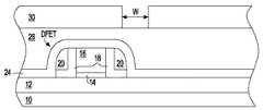
下記の開示に従った本発明の実施形態は、図1の半導体構造体内の金属酸化物半導体電界効果トランジスタFETの基本コンポーネントを用いて、概略断面図が図1に示される金属酸化物半導体電界効果トランジスタFETではなく、特定の金属−絶縁体−金属キャパシタ構造体を提供するように意図されている。そのために、図2乃至図6は、本発明の特定の実施形態による、半導体構造体内に金属−絶縁体−金属キャパシタ構造体を製造する際の進行段階の結果を例示する一連の概略断面図を示す。本発明のこの特定の実施形態は、本発明の第1の特定の実施形態を含む。 Embodiments of the present invention in accordance with the following disclosure use the basic components of a metal oxide semiconductor field effect transistor FET in the semiconductor structure of FIG. 1 and use the basic components of the metal oxide semiconductor field effect shown in FIG. It is intended to provide a specific metal-insulator-metal capacitor structure rather than a transistor FET. To that end, FIGS. 2-6 are a series of schematic cross-sectional views illustrating the results of an advanced stage in fabricating a metal-insulator-metal capacitor structure in a semiconductor structure, according to certain embodiments of the invention. Show. This particular embodiment of the invention includes the first particular embodiment of the invention.
図2は、図2の半導体構造体内のダミー電界効果トランジスタDFETが、図1に示されるような活性領域を含む半導体基板10の部分上ではなく、分離領域12の完全に上に配置され形成される(すなわち、ゲート誘電体14もゲート16も半導体チャネル領域上に配置されない又はその上方に整合されない)限り、ソース及びドレイン領域22がない第1の例における図1の基本的な半導体構造体を示す。 FIG. 2 shows that the dummy field effect transistor DFET in the semiconductor structure of FIG. 2 is disposed and formed completely over the
同様に図1に示されるコンタクト・ビア28も図2内になく、コンタクト・ビア28がないため、図1に示されるライナ層24’はライナ層24として存在し、図1に示される層間誘電体26’は層間誘電体26として存在する。 Similarly, the contact via 28 shown in FIG. 1 is not in FIG. 2 and there is no contact via 28, so the
他の点では、図1及び図2に示されている同様の、類似の、又は同一の層及び構造体は、全く同じに示されている。 In other respects, similar, similar or identical layers and structures shown in FIGS. 1 and 2 are shown identically.
最終的に、図2は、層間誘電体26上に配置され形成され、かつ、ゲート16の一方の側の上にあるがゲート16の他方の側の上にはない、少なくとも部分的に第2のスペーサの上に位置する開口部を含んでいる、マスク30を示す。図2の概略断面図内に示されるように、開口部は、約50ナノメートルから約500ナノメートルまでのライン幅Wを有する。 Finally, FIG. 2 shows at least partly a second arrangement formed and formed on the
マスク30は、幾つかのマスク材料のいずれかを含むことができる。一般には、ハード・マスク材料及びフォトレジスト・マスク材料、並びに、ハード・マスク材料及びフォトレジスト・マスク材料の複合体が含まれる。フォトレジスト・マスク材料は、通常、より一般的なものであり、必ずしも限定されるものではないが、ポジ型フォトレジスト材料、ネガ型フォトレジスト材料、及びポジ型フォトレジスト材料とネガ型フォトレジスト材料の特性を有するハイブリッド型フォトレジスト材料を含むことができる。典型的には、マスク30は、約100ナノメートルから約2000ナノメートルまでの厚さを有するポジ型フォトレジスト材料又はネガ型フォトレジスト材料を含む。 The
図3は、エッチング・マスクとしてマスク30を及びエッチング停止部としてライナ層24を用いながら、層間誘電体26をエッチングして層間誘電体26’’を提供し、開口部Aを定めた結果を示す。同じく半導体製造技術分野において一般に従来のものであるエッチング法を用いながら、エッチング・マスクとしてマスク30を及びエッチング停止部としてライナ層24を用いて、層間誘電体26をエッチングして層間誘電体26’’を形成することができる。特に、限定されるものではないが、湿式化学エッチング法及び乾式プラズマ・エッチング法が含まれる。乾式プラズマ・エッチング法が層間誘電体26’’の真っ直ぐの側壁を可能にする限り、一般に、乾式プラズマ・エッチング法が好ましい。 FIG. 3 shows the result of defining the opening A by etching the
図4は、エッチング・マスクとして、少なくとも層間誘電体26’を、そして同じくマスク30を用いながら、ライナ層24をエッチングして、ライナ層24’’を形成した結果を示す。上記のエッチングは、開口部Aから細長い開口部A’をもたらし、ここではエッチング停止部として用いられる第2のスペーサ20及び分離領域12の部分を露出させる。層間誘電体26’’を形成するための層間誘電体26の上記のエッチングと同様に、ライナ層24’’を形成するためのライナ層24のエッチングは、他の点で半導体製造技術分野において一般に通常のものであるエッチング法及びエッチング材料を用いて行なうこともできる。特に、限定されるものではないが、湿式化学エッチング法及び材料、並びに、乾式プラズマ・エッチング法及び材料も含まれる。乾式プラズマ・エッチング法及び材料が半導体構造体内のエッチングされた構造体に対してほぼ真っ直ぐの側壁をもたらす限り、乾式プラズマ・エッチング法及び材料が好ましい。 FIG. 4 shows the result of etching the
図5は、図4に示される開口部A’に近いゲート16の一方の側から第2のスペーサ20の部分を選択的に除去して、開口部A’から開口部A’’を形成した結果を示す。そのようなエッチングの結果として、第2のスペーサ20’は、開口部A’’とは反対側のゲート16の側において第1のスペーサ18に隣接したままである。他の点では半導体製造技術分野において一般に通常のものであるエッチング法及びエッチング材料を用いながら、第2のスペーサ20の上記部分をエッチングし、第2のスペーサ20’を提供することができる。ここで図3に示される開口部Aと比べて垂直方向にも横方向にも細長い開口部A’’を提供するために、図5との関連において必要とされる不可欠な横方向エッチングを施す等方性エッチング法であることが意図される湿式化学エッチング法及び乾式プラズマ・エッチング法が、特に含まれる。 In FIG. 5, the
図6は、最初に、図5の半導体構造体からマスク30を剥離した結果を示す。マスク30は、他の点では半導体製造技術分野において一般に従来のものである方法及び材料を用いながら、図5の半導体構造体からマスク30を剥離し、図6の半導体構造体を部分的に提供することができる。特に、限定されるものではないが、湿式化学エッチング法、乾式プラズマ・エッチング法、及び湿式化学エッチング法と乾式プラズマ・エッチング法の組み合わせも含まれる。 FIG. 6 shows the result of first removing the
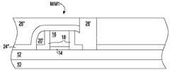
図6は、最終的に、図5に示される開口部A’’内に配置され形成されたコンタクト・ビア28’を示す。図1に示されるコンタクト・ビア28と同様に、図6に示されるコンタクト・ビア28’は、ブランケット層堆積、及び特に化学機械研磨平坦化法のような平坦化法を用いて形成することができる。 FIG. 6 finally shows the contact via 28 ′ disposed and formed within the opening A ″ shown in FIG. 5. Similar to the contact via 28 shown in FIG. 1, the contact via 28 ′ shown in FIG. 6 may be formed using a blanket layer deposition and planarization method, particularly a chemical mechanical polishing planarization method. it can.
図6は、本発明の第1の実施形態を含む本発明の特定の実施形態に従った、半導体構造体の概略断面図を示す。半導体構造体は、垂直型金属−絶縁体−金属キャパシタを含む。垂直型金属−絶縁体−金属キャパシタ内では、ゲート16(すなわち、ゲート材料層)(半導体基板10上に位置する分離領域12上に位置するゲート誘電体14上に配置された)は、キャパシタ・プレートを含む。垂直型金属−絶縁体−金属キャパシタ内では、均一の厚さを有し、ゲート16の横方向に隣り合って接近して配置された第1のスペーサ18は、キャパシタ誘電体を含む。最終的に、垂直型金属−絶縁体−金属キャパシタ内では、第1のスペーサ18の横方向に隣り合って接近して配置されたコンタクト・ビア28’は、別のキャパシタ・プレートを含む。 FIG. 6 shows a schematic cross-sectional view of a semiconductor structure in accordance with certain embodiments of the present invention, including the first embodiment of the present invention. The semiconductor structure includes a vertical metal-insulator-metal capacitor. Within the vertical metal-insulator-metal capacitor, the gate 16 (ie, the gate material layer) (located on the
垂直型金属−絶縁体−金属キャパシタが、垂直型金属−絶縁体−金属キャパシタの垂直方向のスケーリングとの関連において最小量の予測される半導体基板10の面積を占めることができる限り、上記の実施形態に従った垂直型金属−絶縁体−金属キャパシタには価値がある。単一の半導体基板の上に垂直型金属−絶縁体−金属キャパシタを金属酸化物半導体電界効果トランジスタと同時に製造できる限り、垂直型金属−絶縁体−金属キャパシタには、付加的な価値がある。 As long as the vertical metal-insulator-metal capacitor can occupy a minimum amount of expected
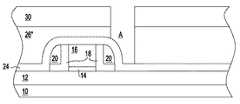
図7及び図8は、概略断面図が図6に示される半導体構造体と関連した半導体構造体の概略断面図及び概略平面図を示す。 7 and 8 show a schematic cross-sectional view and a schematic plan view of a semiconductor structure associated with the semiconductor structure whose schematic cross-sectional view is shown in FIG.
図7は、概略断面図が図6に示される半導体構造体と対応する半導体構造体の概略断面図を示すが、図6に示されるような第1の金属−絶縁体−金属キャパシタMIM1に加えて、図7は、第1の金属−絶縁体−金属キャパシタMIM1の鏡像となる第2の金属−絶縁体−金属キャパシタMIM2を示す。図7の半導体構造体を製造するための処理シーケンスは、図2に示される単一の分離されたダミー金属酸化物半導体電界効果トランジスタDFETではなく、2つの別個のダミー金属酸化物半導体電界効果トランジスタDFETで最初に始まること以外は、図6の半導体構造体を製造するための処理シーケンスと類似している。 FIG. 7 shows a schematic cross-sectional view of a semiconductor structure whose schematic cross-sectional view corresponds to the semiconductor structure shown in FIG. 6, but in addition to the first metal-insulator-metal capacitor MIM1 as shown in FIG. FIG. 7 shows a second metal-insulator-metal capacitor MIM2 that is a mirror image of the first metal-insulator-metal capacitor MIM1. The processing sequence for manufacturing the semiconductor structure of FIG. 7 is not a single isolated dummy metal oxide semiconductor field effect transistor DFET shown in FIG. 2, but two separate dummy metal oxide semiconductor field effect transistors. It is similar to the process sequence for manufacturing the semiconductor structure of FIG. 6 except that it first begins with a DFET.
図8の概略平面図は、ゲート16と、ゲート16を完全に囲むように配置され形成された第1のスペーサ18と、第1のスペーサ18を部分的に囲むように配置され形成された第2のスペーサ20とを示す。図8は、最終的に、図8に示される他の残りの構造体のように層間誘電体26’’の下方に配置されるのではなく、層間誘電体26’’を貫通するコンタクト・ビア28’’及び28’’’を示す。図8内では、明確にするために、ライナ層24’’は省略されている。 The schematic plan view of FIG. 8 shows a
図7及び図8に示される複数の金属−絶縁体−金属キャパシタMIM1及びMIM2は、図6に示される単一の金属−絶縁体−金属キャパシタMIM1の利点の全てを有するが、明らかに付加的な容量が存在する。 The multiple metal-insulator-metal capacitors MIM1 and MIM2 shown in FIGS. 7 and 8 have all of the advantages of the single metal-insulator-metal capacitor MIM1 shown in FIG. Capacity exists.
図9及び図10は、本発明の別の実施形態に従った半導体構造体の概略断面図及び概略平面図を示す。本発明のこの他の実施形態は、本発明の第2の実施形態を含む。本発明のこの特定の第2の実施形態に従ったこの特定の半導体構造体は、図7、図8、又は図6の概略断面図及び平面図内に示される本発明の第1の実施形態と関連している。しかしながら、図9及び図10の概略断面図及び平面図内で、図7、図8及び図6に示される第1のスペーサ18は、ここでは、ゲート16のより近くに配置され形成された第1のサブ層18aと、その上に配置され形成され、かつ、ゲート16からさらに遠くに離間配置された第2のサブ層18bとを含む。 9 and 10 show a schematic cross-sectional view and a schematic plan view of a semiconductor structure according to another embodiment of the present invention. This other embodiment of the present invention includes the second embodiment of the present invention. This particular semiconductor structure according to this particular second embodiment of the present invention is the first embodiment of the present invention shown in the schematic cross-sectional and plan views of FIG. 7, FIG. 8, or FIG. Are related. However, in the schematic cross-sectional views and plan views of FIGS. 9 and 10, the
この第2の実施形態において意図されるのは、約2ナノメートルから約50ナノメートルまでの厚さを有する第1のサブ層18aが、限定されるものではないが、図6、図7及び図8に示される第1のスペーサ18を構成することができる誘電体材料のような誘電体材料を含むことである。同様に第2の実施形態において意図されるのは、約5ナノメートルから約100ナノメートルまでの厚さを有する第2のサブ層18bが導体材料を含むことである。そのような導体材料は、一般に、ゲート16を構成できるものと同じ導体材料で形成することができる。 In this second embodiment, it is contemplated that the
この第2の実施形態においては、導体材料を含む第2のサブ層18bは、初めは導体材料として、又は代替的に非導電性材料の付加的なインサイチュ(in-situ)処理の結果として形成することができる。非導電性材料のそのような付加的なインサイチュ処理は、例えば、必ずしも限定されるものではないが、例えば制限なく、非導電性シリコン材料を含む第2のサブ層18bをサリサイド処理して第2のサブ層18bのための導電性シリサイド材料を提供することができるサリサイド処理を含むことができる。導体材料を含む第2のサブ層18bが最初に導電性材料で形成されようと、又は代替的に、導体材料でインサイチュ形成されようと、概略断面図が図1に示される電界効果トランジスタFETといった同時に形成された電界効果トランジスタから、導電性材料の部分を除去することが望ましい。 In this second embodiment, the
第1の実施形態との関連において上記に挙げられた利点を越えて、導電性の第2のサブ層18bがより大きい容量の接触領域を提供し、よって、より高容量をもたらす限り、概略断面図及び平面図が図9及び図10に示される半導体構造体には価値がある。 Beyond the advantages listed above in the context of the first embodiment, as long as the conductive
本発明の好ましい実施形態は、本発明を限定するものではなく、本発明を説明するものである。好ましい実施形態に従った金属−絶縁体−金属キャパシタを含む半導体構造体の方法、材料、構造体、及び寸法に対して改訂及び修正を施すことができ、本発明に、さらに添付の特許請求の範囲に従って金属−絶縁体−金属キャパシタ及びその製造方法を依然として提供することができる。 The preferred embodiments of the invention are illustrative of the invention rather than limiting of the invention. Revisions and modifications can be made to the methods, materials, structures, and dimensions of semiconductor structures including metal-insulator-metal capacitors according to preferred embodiments, and the present invention further includes the following claims. According to the scope, metal-insulator-metal capacitors and methods for manufacturing the same can still be provided.
10:半導体基板
12:分離領域
14:ゲート誘電体
16:ゲート
18:第1のスペーサ
18a:第1のサブ層
18b:第2のサブ層
20、20’:第2のスペーサ
22:ソース及びドレイン領域
24、24’’、24’’:ライナ層
26、26’、26’’:層間誘電体
28、28’、28’’、28’’’:コンタクト・ビア
30:マスク
A、A’、A’’:開口部10: semiconductor substrate 12: isolation region 14: gate dielectric 16: gate 18:
Claims (18)
Translated fromJapanese前記誘電体分離領域上に配置されたゲート誘電体と、
前記ゲート誘電体上に配置されたゲートと、
前記ゲートの側壁に横方向に接近して配置された均一な厚さのスペーサと、
前記均一な厚さのスペーサの側壁と横方向に接近して配置されたコンタクト・ビアと、
を備える半導体構造体。A dielectric isolation region disposed on a semiconductor substrate;
A gate dielectric disposed on the dielectric isolation region;
A gate disposed on the gate dielectric;
A spacer of uniform thickness disposed laterally close to the sidewall of the gate;
Contact vias disposed laterally close to the sidewalls of the uniform thickness spacer;
A semiconductor structure comprising:
前記ゲートは前記ゲート誘電体上に整合された状態で配置される、
請求項1に記載の半導体構造体。The gate dielectric is disposed only on the isolation region;
The gate is disposed in alignment on the gate dielectric;
The semiconductor structure according to claim 1.
前記コンタクト・ビアは、前記均一な厚さのスペーサの前記側壁に横方向に隣接して配置される、
請求項1に記載の半導体構造体。The uniform thickness spacer is disposed laterally adjacent to the sidewall of the gate;
The contact via is disposed laterally adjacent to the sidewall of the uniform thickness spacer;
The semiconductor structure according to claim 1.
前記付加的な均一な厚さのスペーサに横方向に接近して配置され、かつ、前記コンタクト・ビアから分離された付加的なゲートと、
をさらに備える、請求項1に記載の半導体構造体。An additional uniform thickness spacer also disposed laterally close to the contact via and separated from the uniform thickness spacer;
An additional gate disposed laterally close to the additional uniform thickness spacer and separated from the contact via;
The semiconductor structure according to claim 1, further comprising:
半導体基板の上に配置された誘電体分離領域を含む半導体構造体を準備することと、
前記分離領域上にダミー電界効果トランジスタを形成することであって、前記ダミー電界効果トランジスタは、
前記誘電体分離領域上に形成されたゲート誘電体と、
前記ゲート誘電体上に形成されたゲートと、
前記ゲートの側壁に横方向に接近して形成された均一な厚さのスペーサと、
前記均一な厚さのスペーサ上に形成されたスペーサ形状のスペーサと、
を含む、形成することと、
前記均一な厚さのスペーサからスペーサ形状のスペーサの部分を完全に除去することと、
前記均一な厚さのスペーサの露出された部分上にコンタクト・ビアを形成することと、
を含む前記方法。A method of manufacturing a semiconductor structure, comprising:
Providing a semiconductor structure including a dielectric isolation region disposed on a semiconductor substrate;
Forming a dummy field effect transistor on the isolation region, wherein the dummy field effect transistor comprises:
A gate dielectric formed on the dielectric isolation region;
A gate formed on the gate dielectric;
A uniform thickness spacer formed laterally close to the side wall of the gate;
A spacer-shaped spacer formed on the spacer having a uniform thickness;
Including, forming,
Completely removing a spacer-shaped spacer portion from the uniform thickness spacer;
Forming a contact via on the exposed portion of the uniform thickness spacer;
Including said method.
前記ゲート誘電体が前記分離領域上だけに配置され、
前記ゲートが前記ゲート誘電体上に整合された状態で配置される、
請求項11に記載の方法。In forming the dummy field effect transistor,
The gate dielectric is disposed only on the isolation region;
The gate is aligned with the gate dielectric;
The method of claim 11.
前記コンタクト・ビアを形成することにおいて、前記コンタクト・ビアが前記均一な厚さのスペーサの側壁に横方向に隣接して配置される、
請求項11に記載の方法。In forming the dummy field effect transistor, the uniform thickness spacer is disposed laterally adjacent to the sidewall of the gate;
In forming the contact via, the contact via is disposed laterally adjacent to a side wall of the uniform thickness spacer;
The method of claim 11.
前記除去することは、前記ダミー電界効果トランジスタ及び前記付加的なダミー電界効果トランジスタ内の前記均一な厚さのスペーサから前記スペーサ形状のスペーサの部分を完全に除去し、
前記コンタクト・ビアを形成することは、前記ダミー電界効果トランジスタ及び前記付加的なダミー電界効果トランジスタの各々における前記均一な厚さのスペーサの露出された部分上に前記コンタクト・ビアを形成する、
請求項11に記載の方法。Forming the dummy field effect transistor on the isolation region forms an additional dummy field effect transistor on the isolation region;
The removing completely removes the spacer-shaped spacer portion from the uniform thickness spacer in the dummy field effect transistor and the additional dummy field effect transistor;
Forming the contact via forms the contact via on an exposed portion of the uniform thickness spacer in each of the dummy field effect transistor and the additional dummy field effect transistor;
The method of claim 11.
Applications Claiming Priority (1)
| Application Number | Priority Date | Filing Date | Title |
|---|---|---|---|
| US12/344,697US8017997B2 (en) | 2008-12-29 | 2008-12-29 | Vertical metal-insulator-metal (MIM) capacitor using gate stack, gate spacer and contact via |
Publications (1)
| Publication Number | Publication Date |
|---|---|
| JP2010157704Atrue JP2010157704A (en) | 2010-07-15 |
Family
ID=42283785
Family Applications (1)
| Application Number | Title | Priority Date | Filing Date |
|---|---|---|---|
| JP2009271765APendingJP2010157704A (en) | 2008-12-29 | 2009-11-30 | Vertical metal-insulator-metal (mim) capacitor using gate stack, gate spacer and contact via |
Country Status (3)
| Country | Link |
|---|---|
| US (1) | US8017997B2 (en) |
| JP (1) | JP2010157704A (en) |
| KR (1) | KR20100080315A (en) |
Cited By (1)
| Publication number | Priority date | Publication date | Assignee | Title |
|---|---|---|---|---|
| CN105074916A (en)* | 2013-03-05 | 2015-11-18 | 高通股份有限公司 | Metal-Oxide-Metal (MOM) Capacitors with Enhanced Capacitance |
Families Citing this family (12)
| Publication number | Priority date | Publication date | Assignee | Title |
|---|---|---|---|---|
| US8963223B2 (en)* | 2010-03-01 | 2015-02-24 | Broadcom Corporation | Scalable integrated MIM capacitor using gate metal |
| US8367494B2 (en) | 2011-04-05 | 2013-02-05 | International Business Machines Corporation | Electrical fuse formed by replacement metal gate process |
| US8969922B2 (en)* | 2012-02-08 | 2015-03-03 | Taiwan Semiconductor Manufacturing Company, Ltd. | Field effect transistors and method of forming the same |
| US9142607B2 (en) | 2012-02-23 | 2015-09-22 | Freescale Semiconductor, Inc. | Metal-insulator-metal capacitor |
| US9969613B2 (en) | 2013-04-12 | 2018-05-15 | International Business Machines Corporation | Method for forming micro-electro-mechanical system (MEMS) beam structure |
| KR102065973B1 (en)* | 2013-07-12 | 2020-01-15 | 삼성전자 주식회사 | Semiconductor device and fabricating method thereof |
| US10014843B2 (en)* | 2013-08-08 | 2018-07-03 | Zhuhai Advanced Chip Carriers & Electronic Substrate Solutions Technologies Co. Ltd. | Multilayer electronic structures with embedded filters |
| US9490252B1 (en) | 2015-08-05 | 2016-11-08 | International Business Machines Corporation | MIM capacitor formation in RMG module |
| US10312318B2 (en) | 2015-09-22 | 2019-06-04 | International Business Machines Corporation | Metal-insulator-metal capacitor structure |
| US9893145B1 (en) | 2016-08-09 | 2018-02-13 | International Business Machines Corporation | On chip MIM capacitor |
| US10388572B2 (en) | 2017-03-06 | 2019-08-20 | International Business Machines Corporation | Integrating metal-insulator-metal capacitors with fabrication of vertical field effect transistors |
| US11856801B2 (en)* | 2020-06-16 | 2023-12-26 | Taiwan Semiconductor Manufacturing Company Limited | Threshold voltage-modulated memory device using variable-capacitance and methods of forming the same |
Citations (10)
| Publication number | Priority date | Publication date | Assignee | Title |
|---|---|---|---|---|
| JPH06310671A (en)* | 1993-04-26 | 1994-11-04 | Toshiba Corp | Semiconductor device |
| JPH1079505A (en)* | 1996-09-05 | 1998-03-24 | Hitachi Ltd | Method for manufacturing semiconductor integrated circuit device |
| JP2000091530A (en)* | 1998-09-10 | 2000-03-31 | Nec Corp | Semiconductor device and manufacturing method thereof |
| JP2001118998A (en)* | 1999-10-19 | 2001-04-27 | Mitsubishi Electric Corp | Semiconductor device and method of manufacturing semiconductor device |
| JP2005268551A (en)* | 2004-03-18 | 2005-09-29 | Nec Electronics Corp | Semiconductor device and manufacturing method thereof |
| JP2008098466A (en)* | 2006-10-13 | 2008-04-24 | Elpida Memory Inc | Manufacturing method of semiconductor device |
| JP2008147257A (en)* | 2006-12-06 | 2008-06-26 | Fujitsu Ltd | Electronic device, manufacturing method thereof, and memory device |
| JP2008192883A (en)* | 2007-02-06 | 2008-08-21 | Elpida Memory Inc | Semiconductor device |
| JP2008227049A (en)* | 2007-03-12 | 2008-09-25 | Matsushita Electric Ind Co Ltd | Semiconductor device and manufacturing method thereof |
| JP2008294111A (en)* | 2007-05-23 | 2008-12-04 | Renesas Technology Corp | Manufacturing method of semiconductor device |
Family Cites Families (37)
| Publication number | Priority date | Publication date | Assignee | Title |
|---|---|---|---|---|
| US4753897A (en)* | 1986-03-14 | 1988-06-28 | Motorola Inc. | Method for providing contact separation in silicided devices using false gate |
| US5773341A (en)* | 1996-01-18 | 1998-06-30 | Micron Technology, Inc. | Method of making capacitor and conductive line constructions |
| JPH11135745A (en)* | 1997-10-29 | 1999-05-21 | Toshiba Corp | Semiconductor device and manufacturing method thereof |
| US6228696B1 (en)* | 1998-11-05 | 2001-05-08 | Vantis Corporation | Semiconductor-oxide-semiconductor capacitor formed in integrated circuit |
| US6841821B2 (en)* | 1999-10-07 | 2005-01-11 | Monolithic System Technology, Inc. | Non-volatile memory cell fabricated with slight modification to a conventional logic process and methods of operating same |
| US6559055B2 (en)* | 2000-08-15 | 2003-05-06 | Mosel Vitelic, Inc. | Dummy structures that protect circuit elements during polishing |
| US6451667B1 (en)* | 2000-12-21 | 2002-09-17 | Infineon Technologies Ag | Self-aligned double-sided vertical MIMcap |
| TW546778B (en)* | 2001-04-20 | 2003-08-11 | Koninkl Philips Electronics Nv | Two-transistor flash cell |
| CA2393304C (en)* | 2002-07-15 | 2003-07-22 | Ghislain Simard | Truss assembly apparatus with endless track system |
| US6787836B2 (en)* | 2002-08-21 | 2004-09-07 | International Business Machines Corporation | Integrated metal-insulator-metal capacitor and metal gate transistor |
| US6909145B2 (en)* | 2002-09-23 | 2005-06-21 | International Business Machines Corporation | Metal spacer gate for CMOS FET |
| US6608747B1 (en)* | 2002-09-26 | 2003-08-19 | Oki Electric Industry Co., Ltd. | Variable-capacitance device and voltage-controlled oscillator |
| KR100776503B1 (en)* | 2002-12-02 | 2007-11-15 | 엘지.필립스 엘시디 주식회사 | Pixel Structure of Liquid Crystal Display |
| KR100549269B1 (en)* | 2003-12-31 | 2006-02-03 | 동부아남반도체 주식회사 | Manufacturing method of split gate type flash memory device |
| US7144783B2 (en)* | 2004-04-30 | 2006-12-05 | Intel Corporation | Reducing gate dielectric material to form a metal gate electrode extension |
| JP3998665B2 (en)* | 2004-06-16 | 2007-10-31 | 株式会社ルネサステクノロジ | Semiconductor device and manufacturing method thereof |
| US7704833B2 (en)* | 2004-08-25 | 2010-04-27 | Intel Corporation | Method of forming abrupt source drain metal gate transistors |
| US7902058B2 (en)* | 2004-09-29 | 2011-03-08 | Intel Corporation | Inducing strain in the channels of metal gate transistors |
| KR100882930B1 (en)* | 2004-12-17 | 2009-02-10 | 삼성전자주식회사 | CMOS semiconductor devices having source and drain regions and fabrication methods thereof |
| US7323379B2 (en) | 2005-02-03 | 2008-01-29 | Mosys, Inc. | Fabrication process for increased capacitance in an embedded DRAM memory |
| KR100674958B1 (en)* | 2005-02-23 | 2007-01-26 | 삼성전자주식회사 | Split type flash memory device having self-aligned control gate and manufacturing method thereof |
| US7253481B2 (en)* | 2005-07-14 | 2007-08-07 | Taiwan Semiconductor Manufacturing Company, Ltd. | High performance MOS device with graded silicide |
| KR20070055729A (en)* | 2005-11-28 | 2007-05-31 | 동부일렉트로닉스 주식회사 | Structure of Semiconductor Device Having Dummy Gate and Manufacturing Method Thereof |
| JP2007184323A (en)* | 2006-01-04 | 2007-07-19 | Renesas Technology Corp | Semiconductor device and manufacturing method of semiconductor device |
| JP2007243105A (en)* | 2006-03-13 | 2007-09-20 | Sony Corp | Semiconductor device and manufacturing method thereof |
| US7378308B2 (en)* | 2006-03-30 | 2008-05-27 | Taiwan Semiconductor Manufacturing Company, Ltd. | CMOS devices with improved gap-filling |
| US7514740B2 (en) | 2006-07-10 | 2009-04-07 | Taiwan Semiconductor Manufacturing Company, Ltd. | Logic compatible storage device |
| US7670914B2 (en)* | 2006-09-28 | 2010-03-02 | Globalfoundries Inc. | Methods for fabricating multiple finger transistors |
| US20080093682A1 (en)* | 2006-10-18 | 2008-04-24 | Liang-Gi Yao | Polysilicon levels for silicided structures including MOSFET gate electrodes and 3D devices |
| US8350335B2 (en)* | 2007-04-18 | 2013-01-08 | Sony Corporation | Semiconductor device including off-set spacers formed as a portion of the sidewall |
| US20090087956A1 (en)* | 2007-09-27 | 2009-04-02 | Texas Instruments Incorporated | Dummy Contact Fill to Improve Post Contact Chemical Mechanical Polish Topography |
| DE102007046849B4 (en)* | 2007-09-29 | 2014-11-06 | Advanced Micro Devices, Inc. | Method of making large-gate-gate structures after transistor fabrication |
| US8048752B2 (en)* | 2008-07-24 | 2011-11-01 | Taiwan Semiconductor Manufacturing Company, Ltd. | Spacer shape engineering for void-free gap-filling process |
| US8169031B2 (en)* | 2008-08-26 | 2012-05-01 | International Business Machines Corporation | Continuous metal semiconductor alloy via for interconnects |
| US20100078728A1 (en)* | 2008-08-28 | 2010-04-01 | Taiwan Semiconductor Manufacturing Company, Ltd. | Raise s/d for gate-last ild0 gap filling |
| US20100059823A1 (en)* | 2008-09-10 | 2010-03-11 | Taiwan Semiconductor Manufacturing Company, Ltd. | Resistive device for high-k metal gate technology and method of making |
| US8093116B2 (en)* | 2008-10-06 | 2012-01-10 | Taiwan Semiconductor Manufacturing Company, Ltd. | Method for N/P patterning in a gate last process |
- 2008
- 2008-12-29USUS12/344,697patent/US8017997B2/ennot_activeExpired - Fee Related
- 2009
- 2009-08-21KRKR1020090077706Apatent/KR20100080315A/ennot_activeAbandoned
- 2009-11-30JPJP2009271765Apatent/JP2010157704A/enactivePending
Patent Citations (10)
| Publication number | Priority date | Publication date | Assignee | Title |
|---|---|---|---|---|
| JPH06310671A (en)* | 1993-04-26 | 1994-11-04 | Toshiba Corp | Semiconductor device |
| JPH1079505A (en)* | 1996-09-05 | 1998-03-24 | Hitachi Ltd | Method for manufacturing semiconductor integrated circuit device |
| JP2000091530A (en)* | 1998-09-10 | 2000-03-31 | Nec Corp | Semiconductor device and manufacturing method thereof |
| JP2001118998A (en)* | 1999-10-19 | 2001-04-27 | Mitsubishi Electric Corp | Semiconductor device and method of manufacturing semiconductor device |
| JP2005268551A (en)* | 2004-03-18 | 2005-09-29 | Nec Electronics Corp | Semiconductor device and manufacturing method thereof |
| JP2008098466A (en)* | 2006-10-13 | 2008-04-24 | Elpida Memory Inc | Manufacturing method of semiconductor device |
| JP2008147257A (en)* | 2006-12-06 | 2008-06-26 | Fujitsu Ltd | Electronic device, manufacturing method thereof, and memory device |
| JP2008192883A (en)* | 2007-02-06 | 2008-08-21 | Elpida Memory Inc | Semiconductor device |
| JP2008227049A (en)* | 2007-03-12 | 2008-09-25 | Matsushita Electric Ind Co Ltd | Semiconductor device and manufacturing method thereof |
| JP2008294111A (en)* | 2007-05-23 | 2008-12-04 | Renesas Technology Corp | Manufacturing method of semiconductor device |
Cited By (4)
| Publication number | Priority date | Publication date | Assignee | Title |
|---|---|---|---|---|
| CN105074916A (en)* | 2013-03-05 | 2015-11-18 | 高通股份有限公司 | Metal-Oxide-Metal (MOM) Capacitors with Enhanced Capacitance |
| JP2016511548A (en)* | 2013-03-05 | 2016-04-14 | クアルコム,インコーポレイテッド | Metal-oxide-metal (MOM) capacitors with increased capacitance |
| JP2017076815A (en)* | 2013-03-05 | 2017-04-20 | クアルコム,インコーポレイテッド | Metal-oxide-metal (MOM) capacitors with increased capacitance |
| CN105074916B (en)* | 2013-03-05 | 2018-10-16 | 高通股份有限公司 | Metal-Oxide-Metal (MOM) Capacitors with Enhanced Capacitance |
Also Published As
| Publication number | Publication date |
|---|---|
| US20100163949A1 (en) | 2010-07-01 |
| KR20100080315A (en) | 2010-07-08 |
| US8017997B2 (en) | 2011-09-13 |
Similar Documents
| Publication | Publication Date | Title |
|---|---|---|
| JP2010157704A (en) | Vertical metal-insulator-metal (mim) capacitor using gate stack, gate spacer and contact via | |
| US11282750B2 (en) | Contact structure and method of fabricating the same | |
| US7329953B2 (en) | Structure for reducing leakage currents and high contact resistance for embedded memory and method for making same | |
| TWI715615B (en) | Semiconductor device and fabrication method thereof | |
| US7682896B2 (en) | Trench metal-insulator-metal (MIM) capacitors integrated with middle-of-line metal contacts, and method of fabricating same | |
| US12218209B2 (en) | Contacts for semiconductor devices and methods of forming the same | |
| US6872627B2 (en) | Selective formation of metal gate for dual gate oxide application | |
| US20090101968A1 (en) | Structure of semiconductor device and manufacturing method of the same | |
| US20090096003A1 (en) | Semiconductor cell structure including buried capacitor and method for fabrication thereof | |
| JP2012033939A (en) | Dram access transistor and method for forming the same | |
| JP2007505482A (en) | Metal gate structures and methods of formation in integrated circuit transistors (structures and methods for metal replacement gates in high performance devices) | |
| KR20110124142A (en) | Embedded DRAM for ultra-thin semiconductor-on-insulators | |
| US6335248B1 (en) | Dual workfunction MOSFETs with borderless diffusion contacts for high-performance embedded DRAM technology | |
| CN104701136A (en) | Capacitor, semiconductor device and production method of capacitor | |
| JP2009534833A (en) | Manufacturing method of semiconductor components with high capacitance per unit area | |
| CN115332217A (en) | Capacitor structure and manufacturing method thereof | |
| US20070077715A1 (en) | Semiconductor device and method of fabricating the same | |
| US6930342B2 (en) | Semiconductor memory and method of manufacturing the same | |
| US20080057660A1 (en) | Step-gate for a semiconductor device | |
| US20220199772A1 (en) | Nanosheet semiconductor devices with n/p boundary structure | |
| CN114765177A (en) | Memory cell and method for producing the same | |
| JP4328396B2 (en) | Manufacturing method of memory cell in DRAM | |
| US6245633B1 (en) | Fabrication method for a double-side double-crown stacked capacitor | |
| US11069715B2 (en) | Memory structure | |
| CN116960125A (en) | Multi-stacked semiconductor devices and methods of fabricating the same |
Legal Events
| Date | Code | Title | Description |
|---|---|---|---|
| A621 | Written request for application examination | Free format text:JAPANESE INTERMEDIATE CODE: A621 Effective date:20120611 | |
| A131 | Notification of reasons for refusal | Free format text:JAPANESE INTERMEDIATE CODE: A131 Effective date:20130820 | |
| A521 | Request for written amendment filed | Free format text:JAPANESE INTERMEDIATE CODE: A523 Effective date:20131107 | |
| RD12 | Notification of acceptance of power of sub attorney | Free format text:JAPANESE INTERMEDIATE CODE: A7432 Effective date:20131107 | |
| A521 | Request for written amendment filed | Free format text:JAPANESE INTERMEDIATE CODE: A821 Effective date:20131107 | |
| A131 | Notification of reasons for refusal | Free format text:JAPANESE INTERMEDIATE CODE: A131 Effective date:20140109 | |
| A601 | Written request for extension of time | Free format text:JAPANESE INTERMEDIATE CODE: A601 Effective date:20140408 | |
| A602 | Written permission of extension of time | Free format text:JAPANESE INTERMEDIATE CODE: A602 Effective date:20140411 | |
| A521 | Request for written amendment filed | Free format text:JAPANESE INTERMEDIATE CODE: A523 Effective date:20140507 | |
| A02 | Decision of refusal | Free format text:JAPANESE INTERMEDIATE CODE: A02 Effective date:20140618 | |
| RD14 | Notification of resignation of power of sub attorney | Free format text:JAPANESE INTERMEDIATE CODE: A7434 Effective date:20140701 |