JP2010153813A - Light-emitting device, method of manufacturing the same, and portable telephone - Google Patents
Light-emitting device, method of manufacturing the same, and portable telephoneDownload PDFInfo
- Publication number
- JP2010153813A JP2010153813AJP2009258522AJP2009258522AJP2010153813AJP 2010153813 AJP2010153813 AJP 2010153813AJP 2009258522 AJP2009258522 AJP 2009258522AJP 2009258522 AJP2009258522 AJP 2009258522AJP 2010153813 AJP2010153813 AJP 2010153813A
- Authority
- JP
- Japan
- Prior art keywords
- electrode
- light
- layer
- semiconductor circuit
- light emitting
- Prior art date
- Legal status (The legal status is an assumption and is not a legal conclusion. Google has not performed a legal analysis and makes no representation as to the accuracy of the status listed.)
- Withdrawn
Links
- 238000004519manufacturing processMethods0.000titleclaimsabstractdescription44
- 239000004065semiconductorSubstances0.000claimsabstractdescription139
- 239000000758substrateSubstances0.000claimsabstractdescription124
- 238000000034methodMethods0.000claimsabstractdescription25
- 239000010410layerSubstances0.000claimsdescription174
- 229920005989resinPolymers0.000claimsdescription77
- 239000011347resinSubstances0.000claimsdescription77
- 238000000926separation methodMethods0.000claimsdescription52
- 239000012790adhesive layerSubstances0.000claimsdescription26
- 239000002274desiccantSubstances0.000claimsdescription10
- 239000002245particleSubstances0.000claimsdescription8
- 230000000149penetrating effectEffects0.000claims1
- 239000010408filmSubstances0.000description188
- 239000000463materialSubstances0.000description52
- 239000002585baseSubstances0.000description42
- 239000000835fiberSubstances0.000description39
- 229910052757nitrogenInorganic materials0.000description34
- 239000000126substanceSubstances0.000description32
- 238000005192partitionMethods0.000description25
- -1tungsten nitrideChemical class0.000description23
- 125000006850spacer groupChemical group0.000description20
- XLOMVQKBTHCTTD-UHFFFAOYSA-Nzinc oxideInorganic materials[Zn]=OXLOMVQKBTHCTTD-UHFFFAOYSA-N0.000description19
- ZOKXTWBITQBERF-UHFFFAOYSA-NMolybdenumChemical compound[Mo]ZOKXTWBITQBERF-UHFFFAOYSA-N0.000description17
- 239000011733molybdenumSubstances0.000description17
- 229910052721tungstenInorganic materials0.000description17
- IJGRMHOSHXDMSA-UHFFFAOYSA-NAtomic nitrogenChemical compoundN#NIJGRMHOSHXDMSA-UHFFFAOYSA-N0.000description16
- 229910052750molybdenumInorganic materials0.000description16
- 239000010937tungstenSubstances0.000description16
- WFKWXMTUELFFGS-UHFFFAOYSA-NtungstenChemical compound[W]WFKWXMTUELFFGS-UHFFFAOYSA-N0.000description15
- PXHVJJICTQNCMI-UHFFFAOYSA-NNickelChemical compound[Ni]PXHVJJICTQNCMI-UHFFFAOYSA-N0.000description13
- KDLHZDBZIXYQEI-UHFFFAOYSA-NPalladiumChemical compound[Pd]KDLHZDBZIXYQEI-UHFFFAOYSA-N0.000description13
- 238000002347injectionMethods0.000description13
- 239000007924injectionSubstances0.000description13
- VYPSYNLAJGMNEJ-UHFFFAOYSA-Nsilicon dioxideInorganic materialsO=[Si]=OVYPSYNLAJGMNEJ-UHFFFAOYSA-N0.000description13
- 229910052751metalInorganic materials0.000description12
- 239000002184metalSubstances0.000description12
- 229910052814silicon oxideInorganic materials0.000description12
- 150000001875compoundsChemical class0.000description11
- 239000000203mixtureSubstances0.000description11
- 229910052581Si3N4Inorganic materials0.000description10
- 239000000956alloySubstances0.000description10
- 229910052799carbonInorganic materials0.000description10
- 239000007789gasSubstances0.000description10
- 239000007788liquidSubstances0.000description10
- HQVNEWCFYHHQES-UHFFFAOYSA-Nsilicon nitrideChemical compoundN12[Si]34N5[Si]62N3[Si]51N64HQVNEWCFYHHQES-UHFFFAOYSA-N0.000description10
- QVGXLLKOCUKJST-UHFFFAOYSA-Natomic oxygenChemical compound[O]QVGXLLKOCUKJST-UHFFFAOYSA-N0.000description9
- 239000002131composite materialSubstances0.000description9
- 230000005525hole transportEffects0.000description9
- 239000001301oxygenSubstances0.000description9
- 229910052760oxygenInorganic materials0.000description9
- 229910052710siliconInorganic materials0.000description9
- 239000011787zinc oxideSubstances0.000description9
- AZFHXIBNMPIGOD-UHFFFAOYSA-N4-hydroxypent-3-en-2-one iridiumChemical compound[Ir].CC(O)=CC(C)=O.CC(O)=CC(C)=O.CC(O)=CC(C)=OAZFHXIBNMPIGOD-UHFFFAOYSA-N0.000description8
- XUIMIQQOPSSXEZ-UHFFFAOYSA-NSiliconChemical compound[Si]XUIMIQQOPSSXEZ-UHFFFAOYSA-N0.000description8
- CUJRVFIICFDLGR-UHFFFAOYSA-NacetylacetonateChemical compoundCC(=O)[CH-]C(C)=OCUJRVFIICFDLGR-UHFFFAOYSA-N0.000description8
- 239000011521glassSubstances0.000description8
- 239000010703siliconSubstances0.000description8
- 238000004544sputter depositionMethods0.000description8
- 239000010936titaniumSubstances0.000description8
- 239000000853adhesiveSubstances0.000description7
- 230000001070adhesive effectEffects0.000description7
- 229910045601alloyInorganic materials0.000description7
- 239000013078crystalSubstances0.000description7
- 239000012535impuritySubstances0.000description7
- 229910003437indium oxideInorganic materials0.000description7
- PJXISJQVUVHSOJ-UHFFFAOYSA-Nindium(iii) oxideChemical compound[O-2].[O-2].[O-2].[In+3].[In+3]PJXISJQVUVHSOJ-UHFFFAOYSA-N0.000description7
- QGLKJKCYBOYXKC-UHFFFAOYSA-NnonaoxidotritungstenChemical compoundO=[W]1(=O)O[W](=O)(=O)O[W](=O)(=O)O1QGLKJKCYBOYXKC-UHFFFAOYSA-N0.000description7
- BASFCYQUMIYNBI-UHFFFAOYSA-NplatinumChemical compound[Pt]BASFCYQUMIYNBI-UHFFFAOYSA-N0.000description7
- 239000002356single layerSubstances0.000description7
- 229910001930tungsten oxideInorganic materials0.000description7
- 239000007983Tris bufferSubstances0.000description6
- 229910052782aluminiumInorganic materials0.000description6
- 150000004945aromatic hydrocarbonsChemical class0.000description6
- 239000004020conductorSubstances0.000description6
- 239000010949copperSubstances0.000description6
- 239000010931goldSubstances0.000description6
- 229920001721polyimidePolymers0.000description6
- 125000000391vinyl groupChemical group[H]C([*])=C([H])[H]0.000description6
- 239000000919ceramicSubstances0.000description5
- 229910010272inorganic materialInorganic materials0.000description5
- 229910044991metal oxideInorganic materials0.000description5
- 150000004706metal oxidesChemical class0.000description5
- 229910000476molybdenum oxideInorganic materials0.000description5
- 229910052759nickelInorganic materials0.000description5
- 150000002894organic compoundsChemical class0.000description5
- 230000010355oscillationEffects0.000description5
- PQQKPALAQIIWST-UHFFFAOYSA-NoxomolybdenumChemical compound[Mo]=OPQQKPALAQIIWST-UHFFFAOYSA-N0.000description5
- 229910052763palladiumInorganic materials0.000description5
- 239000010948rhodiumSubstances0.000description5
- 229910052709silverInorganic materials0.000description5
- 229910052719titaniumInorganic materials0.000description5
- ODHXBMXNKOYIBV-UHFFFAOYSA-NtriphenylamineChemical compoundC1=CC=CC=C1N(C=1C=CC=CC=1)C1=CC=CC=C1ODHXBMXNKOYIBV-UHFFFAOYSA-N0.000description5
- 239000002759woven fabricSubstances0.000description5
- 239000011701zincSubstances0.000description5
- ZVFQEOPUXVPSLB-UHFFFAOYSA-N3-(4-tert-butylphenyl)-4-phenyl-5-(4-phenylphenyl)-1,2,4-triazoleChemical compoundC1=CC(C(C)(C)C)=CC=C1C(N1C=2C=CC=CC=2)=NN=C1C1=CC=C(C=2C=CC=CC=2)C=C1ZVFQEOPUXVPSLB-UHFFFAOYSA-N0.000description4
- DHDHJYNTEFLIHY-UHFFFAOYSA-N4,7-diphenyl-1,10-phenanthrolineChemical compoundC1=CC=CC=C1C1=CC=NC2=C1C=CC1=C(C=3C=CC=CC=3)C=CN=C21DHDHJYNTEFLIHY-UHFFFAOYSA-N0.000description4
- 239000004642PolyimideSubstances0.000description4
- RTAQQCXQSZGOHL-UHFFFAOYSA-NTitaniumChemical compound[Ti]RTAQQCXQSZGOHL-UHFFFAOYSA-N0.000description4
- 229910052783alkali metalInorganic materials0.000description4
- 150000001340alkali metalsChemical class0.000description4
- 229910052784alkaline earth metalInorganic materials0.000description4
- 150000001342alkaline earth metalsChemical class0.000description4
- XAGFODPZIPBFFR-UHFFFAOYSA-NaluminiumChemical compound[Al]XAGFODPZIPBFFR-UHFFFAOYSA-N0.000description4
- MWPLVEDNUUSJAV-UHFFFAOYSA-NanthraceneChemical compoundC1=CC=CC2=CC3=CC=CC=C3C=C21MWPLVEDNUUSJAV-UHFFFAOYSA-N0.000description4
- XKRFYHLGVUSROY-UHFFFAOYSA-NargonSubstances[Ar]XKRFYHLGVUSROY-UHFFFAOYSA-N0.000description4
- 230000015572biosynthetic processEffects0.000description4
- XJHCXCQVJFPJIK-UHFFFAOYSA-Mcaesium fluorideChemical compound[F-].[Cs+]XJHCXCQVJFPJIK-UHFFFAOYSA-M0.000description4
- 239000011231conductive fillerSubstances0.000description4
- 229910052802copperInorganic materials0.000description4
- 229910052737goldInorganic materials0.000description4
- AMWRITDGCCNYAT-UHFFFAOYSA-Lhydroxy(oxo)manganese;manganeseChemical compound[Mn].O[Mn]=O.O[Mn]=OAMWRITDGCCNYAT-UHFFFAOYSA-L0.000description4
- 229910052741iridiumInorganic materials0.000description4
- 239000011777magnesiumSubstances0.000description4
- 239000011159matrix materialSubstances0.000description4
- 239000002923metal particleSubstances0.000description4
- 239000010955niobiumSubstances0.000description4
- 239000011368organic materialSubstances0.000description4
- 229920003227poly(N-vinyl carbazole)Polymers0.000description4
- 230000008569processEffects0.000description4
- 125000001424substituent groupChemical group0.000description4
- 229910052715tantalumInorganic materials0.000description4
- FQJQNLKWTRGIEB-UHFFFAOYSA-N2-(4-tert-butylphenyl)-5-[3-[5-(4-tert-butylphenyl)-1,3,4-oxadiazol-2-yl]phenyl]-1,3,4-oxadiazoleChemical compoundC1=CC(C(C)(C)C)=CC=C1C1=NN=C(C=2C=C(C=CC=2)C=2OC(=NN=2)C=2C=CC(=CC=2)C(C)(C)C)O1FQJQNLKWTRGIEB-UHFFFAOYSA-N0.000description3
- UHOVQNZJYSORNB-UHFFFAOYSA-NBenzeneChemical compoundC1=CC=CC=C1UHOVQNZJYSORNB-UHFFFAOYSA-N0.000description3
- RYGMFSIKBFXOCR-UHFFFAOYSA-NCopperChemical compound[Cu]RYGMFSIKBFXOCR-UHFFFAOYSA-N0.000description3
- UFHFLCQGNIYNRP-UHFFFAOYSA-NHydrogenChemical compound[H][H]UFHFLCQGNIYNRP-UHFFFAOYSA-N0.000description3
- YNPNZTXNASCQKK-UHFFFAOYSA-NPhenanthreneNatural productsC1=CC=C2C3=CC=CC=C3C=CC2=C1YNPNZTXNASCQKK-UHFFFAOYSA-N0.000description3
- 239000004952PolyamideSubstances0.000description3
- BQCADISMDOOEFD-UHFFFAOYSA-NSilverChemical compound[Ag]BQCADISMDOOEFD-UHFFFAOYSA-N0.000description3
- DGEZNRSVGBDHLK-UHFFFAOYSA-N[1,10]phenanthrolineChemical compoundC1=CN=C2C3=NC=CC=C3C=CC2=C1DGEZNRSVGBDHLK-UHFFFAOYSA-N0.000description3
- 229910052786argonInorganic materials0.000description3
- 150000001716carbazolesChemical class0.000description3
- 230000001413cellular effectEffects0.000description3
- 229910017052cobaltInorganic materials0.000description3
- 239000010941cobaltSubstances0.000description3
- GUTLYIVDDKVIGB-UHFFFAOYSA-Ncobalt atomChemical compound[Co]GUTLYIVDDKVIGB-UHFFFAOYSA-N0.000description3
- KPUWHANPEXNPJT-UHFFFAOYSA-NdisiloxaneChemical class[SiH3]O[SiH3]KPUWHANPEXNPJT-UHFFFAOYSA-N0.000description3
- 229910052732germaniumInorganic materials0.000description3
- 239000003365glass fiberSubstances0.000description3
- 238000010438heat treatmentMethods0.000description3
- 239000001257hydrogenSubstances0.000description3
- 229910052739hydrogenInorganic materials0.000description3
- AMGQUBHHOARCQH-UHFFFAOYSA-Nindium;oxotinChemical compound[In].[Sn]=OAMGQUBHHOARCQH-UHFFFAOYSA-N0.000description3
- 239000011147inorganic materialSubstances0.000description3
- 150000002500ionsChemical class0.000description3
- GKOZUEZYRPOHIO-UHFFFAOYSA-Niridium atomChemical compound[Ir]GKOZUEZYRPOHIO-UHFFFAOYSA-N0.000description3
- MILUBEOXRNEUHS-UHFFFAOYSA-Niridium(3+)Chemical compound[Ir+3]MILUBEOXRNEUHS-UHFFFAOYSA-N0.000description3
- 230000001678irradiating effectEffects0.000description3
- 125000001997phenyl groupChemical group[H]C1=C([H])C([H])=C(*)C([H])=C1[H]0.000description3
- 238000009832plasma treatmentMethods0.000description3
- 229910052697platinumInorganic materials0.000description3
- 229920002647polyamidePolymers0.000description3
- 229910052703rhodiumInorganic materials0.000description3
- 239000004332silverSubstances0.000description3
- GUVRBAGPIYLISA-UHFFFAOYSA-Ntantalum atomChemical compound[Ta]GUVRBAGPIYLISA-UHFFFAOYSA-N0.000description3
- 229920001187thermosetting polymerPolymers0.000description3
- 229910052725zincInorganic materials0.000description3
- HTPBWAPZAJWXKY-UHFFFAOYSA-Lzinc;quinolin-8-olateChemical compound[Zn+2].C1=CN=C2C([O-])=CC=CC2=C1.C1=CN=C2C([O-])=CC=CC2=C1HTPBWAPZAJWXKY-UHFFFAOYSA-L0.000description3
- UHXOHPVVEHBKKT-UHFFFAOYSA-N1-(2,2-diphenylethenyl)-4-[4-(2,2-diphenylethenyl)phenyl]benzeneChemical groupC=1C=C(C=2C=CC(C=C(C=3C=CC=CC=3)C=3C=CC=CC=3)=CC=2)C=CC=1C=C(C=1C=CC=CC=1)C1=CC=CC=C1UHXOHPVVEHBKKT-UHFFFAOYSA-N0.000description2
- XOYZGLGJSAZOAG-UHFFFAOYSA-N1-n,1-n,4-n-triphenyl-4-n-[4-[4-(n-[4-(n-phenylanilino)phenyl]anilino)phenyl]phenyl]benzene-1,4-diamineChemical groupC1=CC=CC=C1N(C=1C=CC(=CC=1)N(C=1C=CC=CC=1)C=1C=CC(=CC=1)C=1C=CC(=CC=1)N(C=1C=CC=CC=1)C=1C=CC(=CC=1)N(C=1C=CC=CC=1)C=1C=CC=CC=1)C1=CC=CC=C1XOYZGLGJSAZOAG-UHFFFAOYSA-N0.000description2
- IYZMXHQDXZKNCY-UHFFFAOYSA-N1-n,1-n-diphenyl-4-n,4-n-bis[4-(n-phenylanilino)phenyl]benzene-1,4-diamineChemical compoundC1=CC=CC=C1N(C=1C=CC(=CC=1)N(C=1C=CC(=CC=1)N(C=1C=CC=CC=1)C=1C=CC=CC=1)C=1C=CC(=CC=1)N(C=1C=CC=CC=1)C=1C=CC=CC=1)C1=CC=CC=C1IYZMXHQDXZKNCY-UHFFFAOYSA-N0.000description2
- SPDPTFAJSFKAMT-UHFFFAOYSA-N1-n-[4-[4-(n-[4-(3-methyl-n-(3-methylphenyl)anilino)phenyl]anilino)phenyl]phenyl]-4-n,4-n-bis(3-methylphenyl)-1-n-phenylbenzene-1,4-diamineChemical compoundCC1=CC=CC(N(C=2C=CC(=CC=2)N(C=2C=CC=CC=2)C=2C=CC(=CC=2)C=2C=CC(=CC=2)N(C=2C=CC=CC=2)C=2C=CC(=CC=2)N(C=2C=C(C)C=CC=2)C=2C=C(C)C=CC=2)C=2C=C(C)C=CC=2)=C1SPDPTFAJSFKAMT-UHFFFAOYSA-N0.000description2
- BFTIPCRZWILUIY-UHFFFAOYSA-N2,5,8,11-tetratert-butylperyleneChemical groupCC(C)(C)C1=CC(C2=CC(C(C)(C)C)=CC=3C2=C2C=C(C=3)C(C)(C)C)=C3C2=CC(C(C)(C)C)=CC3=C1BFTIPCRZWILUIY-UHFFFAOYSA-N0.000description2
- STTGYIUESPWXOW-UHFFFAOYSA-N2,9-dimethyl-4,7-diphenyl-1,10-phenanthrolineChemical compoundC=12C=CC3=C(C=4C=CC=CC=4)C=C(C)N=C3C2=NC(C)=CC=1C1=CC=CC=C1STTGYIUESPWXOW-UHFFFAOYSA-N0.000description2
- UOCMXZLNHQBBOS-UHFFFAOYSA-N2-(1,3-benzoxazol-2-yl)phenol zincChemical compound[Zn].Oc1ccccc1-c1nc2ccccc2o1.Oc1ccccc1-c1nc2ccccc2o1UOCMXZLNHQBBOS-UHFFFAOYSA-N0.000description2
- GEQBRULPNIVQPP-UHFFFAOYSA-N2-[3,5-bis(1-phenylbenzimidazol-2-yl)phenyl]-1-phenylbenzimidazoleChemical compoundC1=CC=CC=C1N1C2=CC=CC=C2N=C1C1=CC(C=2N(C3=CC=CC=C3N=2)C=2C=CC=CC=2)=CC(C=2N(C3=CC=CC=C3N=2)C=2C=CC=CC=2)=C1GEQBRULPNIVQPP-UHFFFAOYSA-N0.000description2
- QYNTUCBQEHUHCS-UHFFFAOYSA-N4-n-(3-methylphenyl)-1-n-[4-[4-(n-[4-(n-(3-methylphenyl)anilino)phenyl]anilino)phenyl]phenyl]-1-n,4-n-diphenylbenzene-1,4-diamineChemical groupCC1=CC=CC(N(C=2C=CC=CC=2)C=2C=CC(=CC=2)N(C=2C=CC=CC=2)C=2C=CC(=CC=2)C=2C=CC(=CC=2)N(C=2C=CC=CC=2)C=2C=CC(=CC=2)N(C=2C=CC=CC=2)C=2C=C(C)C=CC=2)=C1QYNTUCBQEHUHCS-UHFFFAOYSA-N0.000description2
- VIZUPBYFLORCRA-UHFFFAOYSA-N9,10-dinaphthalen-2-ylanthraceneChemical compoundC12=CC=CC=C2C(C2=CC3=CC=CC=C3C=C2)=C(C=CC=C2)C2=C1C1=CC=C(C=CC=C2)C2=C1VIZUPBYFLORCRA-UHFFFAOYSA-N0.000description2
- FCNCGHJSNVOIKE-UHFFFAOYSA-N9,10-diphenylanthraceneChemical compoundC1=CC=CC=C1C(C1=CC=CC=C11)=C(C=CC=C2)C2=C1C1=CC=CC=C1FCNCGHJSNVOIKE-UHFFFAOYSA-N0.000description2
- UQVFZEYHQJJGPD-UHFFFAOYSA-N9-[4-(10-phenylanthracen-9-yl)phenyl]carbazoleChemical compoundC1=CC=CC=C1C(C1=CC=CC=C11)=C(C=CC=C2)C2=C1C1=CC=C(N2C3=CC=CC=C3C3=CC=CC=C32)C=C1UQVFZEYHQJJGPD-UHFFFAOYSA-N0.000description2
- VFUDMQLBKNMONU-UHFFFAOYSA-N9-[4-(4-carbazol-9-ylphenyl)phenyl]carbazoleChemical groupC12=CC=CC=C2C2=CC=CC=C2N1C1=CC=C(C=2C=CC(=CC=2)N2C3=CC=CC=C3C3=CC=CC=C32)C=C1VFUDMQLBKNMONU-UHFFFAOYSA-N0.000description2
- SXGIRTCIFPJUEQ-UHFFFAOYSA-N9-anthracen-9-ylanthraceneChemical groupC1=CC=CC2=CC3=CC=CC=C3C(C=3C4=CC=CC=C4C=C4C=CC=CC4=3)=C21SXGIRTCIFPJUEQ-UHFFFAOYSA-N0.000description2
- 102100025982BMP/retinoic acid-inducible neural-specific protein 1Human genes0.000description2
- OKTJSMMVPCPJKN-UHFFFAOYSA-NCarbonChemical compound[C]OKTJSMMVPCPJKN-UHFFFAOYSA-N0.000description2
- CURLTUGMZLYLDI-UHFFFAOYSA-NCarbon dioxideChemical compoundO=C=OCURLTUGMZLYLDI-UHFFFAOYSA-N0.000description2
- 108091006149Electron carriersProteins0.000description2
- 101000933342Homo sapiens BMP/retinoic acid-inducible neural-specific protein 1Proteins0.000description2
- 101000715194Homo sapiens Cell cycle and apoptosis regulator protein 2Proteins0.000description2
- XEEYBQQBJWHFJM-UHFFFAOYSA-NIronChemical compound[Fe]XEEYBQQBJWHFJM-UHFFFAOYSA-N0.000description2
- FYYHWMGAXLPEAU-UHFFFAOYSA-NMagnesiumChemical compound[Mg]FYYHWMGAXLPEAU-UHFFFAOYSA-N0.000description2
- 229910052779NeodymiumInorganic materials0.000description2
- OAICVXFJPJFONN-UHFFFAOYSA-NPhosphorusChemical compound[P]OAICVXFJPJFONN-UHFFFAOYSA-N0.000description2
- 229920001609Poly(3,4-ethylenedioxythiophene)Polymers0.000description2
- 239000004695Polyether sulfoneSubstances0.000description2
- KJTLSVCANCCWHF-UHFFFAOYSA-NRutheniumChemical compound[Ru]KJTLSVCANCCWHF-UHFFFAOYSA-N0.000description2
- 229910006404SnO 2Inorganic materials0.000description2
- 229910052769YtterbiumInorganic materials0.000description2
- HCHKCACWOHOZIP-UHFFFAOYSA-NZincChemical compound[Zn]HCHKCACWOHOZIP-UHFFFAOYSA-N0.000description2
- XHCLAFWTIXFWPH-UHFFFAOYSA-N[O-2].[O-2].[O-2].[O-2].[O-2].[V+5].[V+5]Chemical compound[O-2].[O-2].[O-2].[O-2].[O-2].[V+5].[V+5]XHCLAFWTIXFWPH-UHFFFAOYSA-N0.000description2
- AZWHFTKIBIQKCA-UHFFFAOYSA-N[Sn+2]=O.[O-2].[In+3]Chemical compound[Sn+2]=O.[O-2].[In+3]AZWHFTKIBIQKCA-UHFFFAOYSA-N0.000description2
- SORGEQQSQGNZFI-UHFFFAOYSA-N[azido(phenoxy)phosphoryl]oxybenzeneChemical compoundC=1C=CC=CC=1OP(=O)(N=[N+]=[N-])OC1=CC=CC=C1SORGEQQSQGNZFI-UHFFFAOYSA-N0.000description2
- 125000005595acetylacetonate groupChemical group0.000description2
- NIXOWILDQLNWCW-UHFFFAOYSA-Nacrylic acid groupChemical groupC(C=C)(=O)ONIXOWILDQLNWCW-UHFFFAOYSA-N0.000description2
- REDXJYDRNCIFBQ-UHFFFAOYSA-Naluminium(3+)Chemical compound[Al+3]REDXJYDRNCIFBQ-UHFFFAOYSA-N0.000description2
- 150000001408amidesChemical class0.000description2
- 125000005605benzo groupChemical group0.000description2
- UMIVXZPTRXBADB-UHFFFAOYSA-NbenzocyclobuteneChemical compoundC1=CC=C2CCC2=C1UMIVXZPTRXBADB-UHFFFAOYSA-N0.000description2
- 239000004305biphenylSubstances0.000description2
- UFVXQDWNSAGPHN-UHFFFAOYSA-Kbis[(2-methylquinolin-8-yl)oxy]-(4-phenylphenoxy)alumaneChemical compound[Al+3].C1=CC=C([O-])C2=NC(C)=CC=C21.C1=CC=C([O-])C2=NC(C)=CC=C21.C1=CC([O-])=CC=C1C1=CC=CC=C1UFVXQDWNSAGPHN-UHFFFAOYSA-K0.000description2
- 210000000481breastAnatomy0.000description2
- XZCJVWCMJYNSQO-UHFFFAOYSA-Nbutyl pbdChemical compoundC1=CC(C(C)(C)C)=CC=C1C1=NN=C(C=2C=CC(=CC=2)C=2C=CC=CC=2)O1XZCJVWCMJYNSQO-UHFFFAOYSA-N0.000description2
- 239000011575calciumSubstances0.000description2
- 239000013522chelantSubstances0.000description2
- 239000011651chromiumSubstances0.000description2
- 150000004696coordination complexChemical class0.000description2
- VPUGDVKSAQVFFS-UHFFFAOYSA-NcoroneneChemical compoundC1=C(C2=C34)C=CC3=CC=C(C=C3)C4=C4C3=CC=C(C=C3)C4=C2C3=C1VPUGDVKSAQVFFS-UHFFFAOYSA-N0.000description2
- 230000008878couplingEffects0.000description2
- 238000010168coupling processMethods0.000description2
- 238000005859coupling reactionMethods0.000description2
- 230000006378damageEffects0.000description2
- AJNVQOSZGJRYEI-UHFFFAOYSA-Ndigallium;oxygen(2-)Chemical compound[O-2].[O-2].[O-2].[Ga+3].[Ga+3]AJNVQOSZGJRYEI-UHFFFAOYSA-N0.000description2
- ZUOUZKKEUPVFJK-UHFFFAOYSA-NdiphenylChemical compoundC1=CC=CC=C1C1=CC=CC=C1ZUOUZKKEUPVFJK-UHFFFAOYSA-N0.000description2
- 208000028659dischargeDiseases0.000description2
- 239000003822epoxy resinSubstances0.000description2
- 238000005530etchingMethods0.000description2
- ADHNFLCTOCFIFV-UHFFFAOYSA-Neuropium(3+) 1,10-phenanthrolineChemical compound[Eu+3].c1cnc2c(c1)ccc1cccnc21ADHNFLCTOCFIFV-UHFFFAOYSA-N0.000description2
- 230000005284excitationEffects0.000description2
- 125000001153fluoro groupChemical groupF*0.000description2
- 229910052733galliumInorganic materials0.000description2
- 229910001195gallium oxideInorganic materials0.000description2
- GNPVGFCGXDBREM-UHFFFAOYSA-Ngermanium atomChemical compound[Ge]GNPVGFCGXDBREM-UHFFFAOYSA-N0.000description2
- PCHJSUWPFVWCPO-UHFFFAOYSA-NgoldChemical compound[Au]PCHJSUWPFVWCPO-UHFFFAOYSA-N0.000description2
- 150000002484inorganic compoundsChemical class0.000description2
- 239000011810insulating materialSubstances0.000description2
- 239000012212insulatorSubstances0.000description2
- AOZVYCYMTUWJHJ-UHFFFAOYSA-Kiridium(3+) pyridine-2-carboxylateChemical compound[Ir+3].[O-]C(=O)C1=CC=CC=N1.[O-]C(=O)C1=CC=CC=N1.[O-]C(=O)C1=CC=CC=N1AOZVYCYMTUWJHJ-UHFFFAOYSA-K0.000description2
- 238000009940knittingMethods0.000description2
- 229910052749magnesiumInorganic materials0.000description2
- BBNZOXKLBAWRSH-UHFFFAOYSA-Nn,9-diphenyl-n-[4-(10-phenylanthracen-9-yl)phenyl]carbazol-3-amineChemical compoundC1=CC=CC=C1N(C=1C=C2C3=CC=CC=C3N(C=3C=CC=CC=3)C2=CC=1)C1=CC=C(C=2C3=CC=CC=C3C(C=3C=CC=CC=3)=C3C=CC=CC3=2)C=C1BBNZOXKLBAWRSH-UHFFFAOYSA-N0.000description2
- AJNJGJDDJIBTBP-UHFFFAOYSA-Nn-(9,10-diphenylanthracen-2-yl)-n,9-diphenylcarbazol-3-amineChemical compoundC1=CC=CC=C1N(C=1C=C2C(C=3C=CC=CC=3)=C3C=CC=CC3=C(C=3C=CC=CC=3)C2=CC=1)C1=CC=C(N(C=2C=CC=CC=2)C=2C3=CC=CC=2)C3=C1AJNJGJDDJIBTBP-UHFFFAOYSA-N0.000description2
- IBHBKWKFFTZAHE-UHFFFAOYSA-Nn-[4-[4-(n-naphthalen-1-ylanilino)phenyl]phenyl]-n-phenylnaphthalen-1-amineChemical groupC1=CC=CC=C1N(C=1C2=CC=CC=C2C=CC=1)C1=CC=C(C=2C=CC(=CC=2)N(C=2C=CC=CC=2)C=2C3=CC=CC=C3C=CC=2)C=C1IBHBKWKFFTZAHE-UHFFFAOYSA-N0.000description2
- 229910052758niobiumInorganic materials0.000description2
- GUCVJGMIXFAOAE-UHFFFAOYSA-Nniobium atomChemical compound[Nb]GUCVJGMIXFAOAE-UHFFFAOYSA-N0.000description2
- 150000004767nitridesChemical class0.000description2
- 239000004745nonwoven fabricSubstances0.000description2
- 230000003287optical effectEffects0.000description2
- 239000003960organic solventSubstances0.000description2
- 229910052762osmiumInorganic materials0.000description2
- SYQBFIAQOQZEGI-UHFFFAOYSA-Nosmium atomChemical compound[Os]SYQBFIAQOQZEGI-UHFFFAOYSA-N0.000description2
- 230000003647oxidationEffects0.000description2
- 238000007254oxidation reactionMethods0.000description2
- 230000000737periodic effectEffects0.000description2
- 125000002080perylenyl groupChemical groupC1(=CC=C2C=CC=C3C4=CC=CC5=CC=CC(C1=C23)=C45)*0.000description2
- CSHWQDPOILHKBI-UHFFFAOYSA-NperyreneNatural productsC1=CC(C2=CC=CC=3C2=C2C=CC=3)=C3C2=CC=CC3=C1CSHWQDPOILHKBI-UHFFFAOYSA-N0.000description2
- 229910052698phosphorusInorganic materials0.000description2
- 239000011574phosphorusSubstances0.000description2
- IEQIEDJGQAUEQZ-UHFFFAOYSA-NphthalocyanineChemical classN1C(N=C2C3=CC=CC=C3C(N=C3C4=CC=CC=C4C(=N4)N3)=N2)=C(C=CC=C2)C2=C1N=C1C2=CC=CC=C2C4=N1IEQIEDJGQAUEQZ-UHFFFAOYSA-N0.000description2
- 238000005268plasma chemical vapour depositionMethods0.000description2
- 229920000078poly(4-vinyltriphenylamine)Polymers0.000description2
- 229920005668polycarbonate resinPolymers0.000description2
- 239000004431polycarbonate resinSubstances0.000description2
- 229920000647polyepoxidePolymers0.000description2
- 229920006393polyether sulfonePolymers0.000description2
- 229920000139polyethylene terephthalatePolymers0.000description2
- 239000005020polyethylene terephthalateSubstances0.000description2
- 239000009719polyimide resinSubstances0.000description2
- 229920000642polymerPolymers0.000description2
- 238000003825pressingMethods0.000description2
- 229910052761rare earth metalInorganic materials0.000description2
- MHOVAHRLVXNVSD-UHFFFAOYSA-Nrhodium atomChemical compound[Rh]MHOVAHRLVXNVSD-UHFFFAOYSA-N0.000description2
- YYMBJDOZVAITBP-UHFFFAOYSA-NrubreneChemical compoundC1=CC=CC=C1C(C1=C(C=2C=CC=CC=2)C2=CC=CC=C2C(C=2C=CC=CC=2)=C11)=C(C=CC=C2)C2=C1C1=CC=CC=C1YYMBJDOZVAITBP-UHFFFAOYSA-N0.000description2
- 229910052707rutheniumInorganic materials0.000description2
- 238000007493shaping processMethods0.000description2
- 239000007787solidSubstances0.000description2
- 238000004381surface treatmentMethods0.000description2
- 229920005992thermoplastic resinPolymers0.000description2
- 239000010409thin filmSubstances0.000description2
- TVIVIEFSHFOWTE-UHFFFAOYSA-Ktri(quinolin-8-yloxy)alumaneChemical compound[Al+3].C1=CN=C2C([O-])=CC=CC2=C1.C1=CN=C2C([O-])=CC=CC2=C1.C1=CN=C2C([O-])=CC=CC2=C1TVIVIEFSHFOWTE-UHFFFAOYSA-K0.000description2
- 229910001935vanadium oxideInorganic materials0.000description2
- XLYOFNOQVPJJNP-UHFFFAOYSA-NwaterSubstancesOXLYOFNOQVPJJNP-UHFFFAOYSA-N0.000description2
- OYQCBJZGELKKPM-UHFFFAOYSA-Nzinc indium(3+) oxygen(2-)Chemical compound[O-2].[Zn+2].[O-2].[In+3]OYQCBJZGELKKPM-UHFFFAOYSA-N0.000description2
- 229910052726zirconiumInorganic materials0.000description2
- IWZZBBJTIUYDPZ-DVACKJPTSA-N(z)-4-hydroxypent-3-en-2-one;iridium;2-phenylpyridineChemical compound[Ir].C\C(O)=C\C(C)=O.[C-]1=CC=CC=C1C1=CC=CC=N1.[C-]1=CC=CC=C1C1=CC=CC=N1IWZZBBJTIUYDPZ-DVACKJPTSA-N0.000description1
- JYEUMXHLPRZUAT-UHFFFAOYSA-N1,2,3-triazineChemical compoundC1=CN=NN=C1JYEUMXHLPRZUAT-UHFFFAOYSA-N0.000description1
- RTSZQXSYCGBHMO-UHFFFAOYSA-N1,2,4-trichloro-3-prop-1-ynoxybenzeneChemical compoundCC#COC1=C(Cl)C=CC(Cl)=C1ClRTSZQXSYCGBHMO-UHFFFAOYSA-N0.000description1
- FQIHKGMNFAMMEQ-UHFFFAOYSA-N1-(3,5-diphenylphenyl)anthraceneChemical compoundC1=CC=CC=C1C1=CC(C=2C=CC=CC=2)=CC(C=2C3=CC4=CC=CC=C4C=C3C=CC=2)=C1FQIHKGMNFAMMEQ-UHFFFAOYSA-N0.000description1
- YZMIEPNNVHZOGG-UHFFFAOYSA-N1-(4-methylphenyl)tetracene-5,11-diamineChemical compoundCC1=CC=C(C=C1)C1=CC=CC2=C(C3=CC4=CC=CC=C4C(=C3C=C12)N)NYZMIEPNNVHZOGG-UHFFFAOYSA-N0.000description1
- HDMYKJVSQIHZLM-UHFFFAOYSA-N1-[3,5-di(pyren-1-yl)phenyl]pyreneChemical compoundC1=CC(C=2C=C(C=C(C=2)C=2C3=CC=C4C=CC=C5C=CC(C3=C54)=CC=2)C=2C3=CC=C4C=CC=C5C=CC(C3=C54)=CC=2)=C2C=CC3=CC=CC4=CC=C1C2=C43HDMYKJVSQIHZLM-UHFFFAOYSA-N0.000description1
- XQUPVDVFXZDTLT-UHFFFAOYSA-N1-[4-[[4-(2,5-dioxopyrrol-1-yl)phenyl]methyl]phenyl]pyrrole-2,5-dioneChemical compoundO=C1C=CC(=O)N1C(C=C1)=CC=C1CC1=CC=C(N2C(C=CC2=O)=O)C=C1XQUPVDVFXZDTLT-UHFFFAOYSA-N0.000description1
- FQNVFRPAQRVHKO-UHFFFAOYSA-N1-n,4-n-bis(4-methylphenyl)-1-n,4-n-diphenylbenzene-1,4-diamineChemical compoundC1=CC(C)=CC=C1N(C=1C=CC(=CC=1)N(C=1C=CC=CC=1)C=1C=CC(C)=CC=1)C1=CC=CC=C1FQNVFRPAQRVHKO-UHFFFAOYSA-N0.000description1
- VOIVTTPPKHORBL-UHFFFAOYSA-N1-naphthalen-1-ylanthraceneChemical compoundC1=CC=C2C(C=3C4=CC5=CC=CC=C5C=C4C=CC=3)=CC=CC2=C1VOIVTTPPKHORBL-UHFFFAOYSA-N0.000description1
- OOWLPGTVRWFLCX-UHFFFAOYSA-N2,3,6,7-tetramethyl-9,10-dinaphthalen-1-ylanthraceneChemical compoundC1=CC=C2C(C=3C4=CC(C)=C(C)C=C4C(C=4C5=CC=CC=C5C=CC=4)=C4C=C(C(=CC4=3)C)C)=CC=CC2=C1OOWLPGTVRWFLCX-UHFFFAOYSA-N0.000description1
- JEBPFDQAOYARIB-UHFFFAOYSA-N2,3,6,7-tetramethyl-9,10-dinaphthalen-2-ylanthraceneChemical compoundC1=CC=CC2=CC(C=3C4=CC(C)=C(C)C=C4C(C=4C=C5C=CC=CC5=CC=4)=C4C=C(C(=CC4=3)C)C)=CC=C21JEBPFDQAOYARIB-UHFFFAOYSA-N0.000description1
- IZJOTDOLRQTPHC-UHFFFAOYSA-N2-(4-carbazol-9-ylphenyl)-5-phenyl-1,3,4-oxadiazoleChemical compoundC1=CC=CC=C1C1=NN=C(C=2C=CC(=CC=2)N2C3=CC=CC=C3C3=CC=CC=C32)O1IZJOTDOLRQTPHC-UHFFFAOYSA-N0.000description1
- QUOSAXMWQSSMJW-UHFFFAOYSA-N2-[2,6-bis[2-[4-(dimethylamino)phenyl]ethenyl]pyran-4-ylidene]propanedinitrileChemical compoundC1=CC(N(C)C)=CC=C1C=CC1=CC(=C(C#N)C#N)C=C(C=CC=2C=CC(=CC=2)N(C)C)O1QUOSAXMWQSSMJW-UHFFFAOYSA-N0.000description1
- YLYPIBBGWLKELC-RMKNXTFCSA-N2-[2-[(e)-2-[4-(dimethylamino)phenyl]ethenyl]-6-methylpyran-4-ylidene]propanedinitrileChemical compoundC1=CC(N(C)C)=CC=C1\C=C\C1=CC(=C(C#N)C#N)C=C(C)O1YLYPIBBGWLKELC-RMKNXTFCSA-N0.000description1
- IXHWGNYCZPISET-UHFFFAOYSA-N2-[4-(dicyanomethylidene)-2,3,5,6-tetrafluorocyclohexa-2,5-dien-1-ylidene]propanedinitrileChemical compoundFC1=C(F)C(=C(C#N)C#N)C(F)=C(F)C1=C(C#N)C#NIXHWGNYCZPISET-UHFFFAOYSA-N0.000description1
- HONWGFNQCPRRFM-UHFFFAOYSA-N2-n-(3-methylphenyl)-1-n,1-n,2-n-triphenylbenzene-1,2-diamineChemical compoundCC1=CC=CC(N(C=2C=CC=CC=2)C=2C(=CC=CC=2)N(C=2C=CC=CC=2)C=2C=CC=CC=2)=C1HONWGFNQCPRRFM-UHFFFAOYSA-N0.000description1
- 1250000016222-naphthyl groupChemical group[H]C1=C([H])C([H])=C2C([H])=C(*)C([H])=C([H])C2=C1[H]0.000description1
- VQGHOUODWALEFC-UHFFFAOYSA-N2-phenylpyridineChemical compoundC1=CC=CC=C1C1=CC=CC=N1VQGHOUODWALEFC-UHFFFAOYSA-N0.000description1
- MNHPNCZSKTUPMB-UHFFFAOYSA-N2-tert-butyl-9,10-bis(4-phenylphenyl)anthraceneChemical compoundC=12C=CC=CC2=C(C=2C=CC(=CC=2)C=2C=CC=CC=2)C2=CC(C(C)(C)C)=CC=C2C=1C(C=C1)=CC=C1C1=CC=CC=C1MNHPNCZSKTUPMB-UHFFFAOYSA-N0.000description1
- OBAJPWYDYFEBTF-UHFFFAOYSA-N2-tert-butyl-9,10-dinaphthalen-2-ylanthraceneChemical compoundC1=CC=CC2=CC(C3=C4C=CC=CC4=C(C=4C=C5C=CC=CC5=CC=4)C4=CC=C(C=C43)C(C)(C)C)=CC=C21OBAJPWYDYFEBTF-UHFFFAOYSA-N0.000description1
- WBPXZSIKOVBSAS-UHFFFAOYSA-N2-tert-butylanthraceneChemical compoundC1=CC=CC2=CC3=CC(C(C)(C)C)=CC=C3C=C21WBPXZSIKOVBSAS-UHFFFAOYSA-N0.000description1
- GRTDQSRHHHDWSQ-UHFFFAOYSA-N3,6-diphenyl-9-[4-(10-phenylanthracen-9-yl)phenyl]carbazoleChemical compoundC1=CC=CC=C1C1=CC=C(N(C=2C=CC(=CC=2)C=2C3=CC=CC=C3C(C=3C=CC=CC=3)=C3C=CC=CC3=2)C=2C3=CC(=CC=2)C=2C=CC=CC=2)C3=C1GRTDQSRHHHDWSQ-UHFFFAOYSA-N0.000description1
- TVMBOHMLKCZFFW-UHFFFAOYSA-N3-N,6-N,9-triphenyl-3-N,6-N-bis(9-phenylcarbazol-3-yl)carbazole-3,6-diamineChemical compoundC1=CC=CC=C1N(C=1C=C2C3=CC(=CC=C3N(C=3C=CC=CC=3)C2=CC=1)N(C=1C=CC=CC=1)C=1C=C2C3=CC=CC=C3N(C=3C=CC=CC=3)C2=CC=1)C1=CC=C(N(C=2C=CC=CC=2)C=2C3=CC=CC=2)C3=C1TVMBOHMLKCZFFW-UHFFFAOYSA-N0.000description1
- HXWWMGJBPGRWRS-CMDGGOBGSA-N4- -2-tert-butyl-6- -4h-pyranChemical compoundO1C(C(C)(C)C)=CC(=C(C#N)C#N)C=C1\C=C\C1=CC(C(CCN2CCC3(C)C)(C)C)=C2C3=C1HXWWMGJBPGRWRS-CMDGGOBGSA-N0.000description1
- YLYPIBBGWLKELC-UHFFFAOYSA-N4-(dicyanomethylene)-2-methyl-6-(4-(dimethylamino)styryl)-4H-pyranChemical compoundC1=CC(N(C)C)=CC=C1C=CC1=CC(=C(C#N)C#N)C=C(C)O1YLYPIBBGWLKELC-UHFFFAOYSA-N0.000description1
- ZNJRONVKWRHYBF-VOTSOKGWSA-N4-(dicyanomethylene)-2-methyl-6-julolidyl-9-enyl-4h-pyranChemical compoundO1C(C)=CC(=C(C#N)C#N)C=C1\C=C\C1=CC(CCCN2CCC3)=C2C3=C1ZNJRONVKWRHYBF-VOTSOKGWSA-N0.000description1
- LGDCSNDMFFFSHY-UHFFFAOYSA-N4-butyl-n,n-diphenylanilinePolymersC1=CC(CCCC)=CC=C1N(C=1C=CC=CC=1)C1=CC=CC=C1LGDCSNDMFFFSHY-UHFFFAOYSA-N0.000description1
- 1250000012554-fluorophenyl groupChemical group[H]C1=C([H])C(*)=C([H])C([H])=C1F0.000description1
- IJVFZXJHZBXCJC-UHFFFAOYSA-N4-n-[4-(9,10-diphenylanthracen-2-yl)phenyl]-1-n,1-n,4-n-triphenylbenzene-1,4-diamineChemical compoundC1=CC=CC=C1N(C=1C=CC(=CC=1)N(C=1C=CC=CC=1)C=1C=CC(=CC=1)C=1C=C2C(C=3C=CC=CC=3)=C3C=CC=CC3=C(C=3C=CC=CC=3)C2=CC=1)C1=CC=CC=C1IJVFZXJHZBXCJC-UHFFFAOYSA-N0.000description1
- KLNDKWAYVMOOFU-UHFFFAOYSA-N4-n-[9,10-bis(2-phenylphenyl)anthracen-2-yl]-1-n,1-n,4-n-triphenylbenzene-1,4-diamineChemical compoundC1=CC=CC=C1N(C=1C=CC(=CC=1)N(C=1C=CC=CC=1)C=1C=C2C(C=3C(=CC=CC=3)C=3C=CC=CC=3)=C3C=CC=CC3=C(C=3C(=CC=CC=3)C=3C=CC=CC=3)C2=CC=1)C1=CC=CC=C1KLNDKWAYVMOOFU-UHFFFAOYSA-N0.000description1
- KIYZNTXHGDXHQH-UHFFFAOYSA-N5,12-diphenyl-6,11-bis(4-phenylphenyl)tetraceneChemical compoundC1=CC=CC=C1C1=CC=C(C=2C3=C(C=4C=CC=CC=4)C4=CC=CC=C4C(C=4C=CC=CC=4)=C3C(C=3C=CC(=CC=3)C=3C=CC=CC=3)=C3C=CC=CC3=2)C=C1KIYZNTXHGDXHQH-UHFFFAOYSA-N0.000description1
- MWQDBYKWEGXSJW-UHFFFAOYSA-N6,12-dimethoxy-5,11-diphenylchryseneChemical compoundC12=C3C=CC=CC3=C(OC)C(C=3C=CC=CC=3)=C2C2=CC=CC=C2C(OC)=C1C1=CC=CC=C1MWQDBYKWEGXSJW-UHFFFAOYSA-N0.000description1
- UOOBIWAELCOCHK-BQYQJAHWSA-N870075-87-9Chemical compoundO1C(C(C)C)=CC(=C(C#N)C#N)C=C1\C=C\C1=CC(C(CCN2CCC3(C)C)(C)C)=C2C3=C1UOOBIWAELCOCHK-BQYQJAHWSA-N0.000description1
- NKEZXXDRXPPROK-UHFFFAOYSA-N9,10-bis(2-naphthalen-1-ylphenyl)anthraceneChemical compoundC12=CC=CC=C2C(C2=CC=CC=C2C=2C3=CC=CC=C3C=CC=2)=C(C=CC=C2)C2=C1C1=CC=CC=C1C1=CC=CC2=CC=CC=C12NKEZXXDRXPPROK-UHFFFAOYSA-N0.000description1
- USIXUMGAHVBSHQ-UHFFFAOYSA-N9,10-bis(3,5-diphenylphenyl)anthraceneChemical compoundC1=CC=CC=C1C1=CC(C=2C=CC=CC=2)=CC(C=2C3=CC=CC=C3C(C=3C=C(C=C(C=3)C=3C=CC=CC=3)C=3C=CC=CC=3)=C3C=CC=CC3=2)=C1USIXUMGAHVBSHQ-UHFFFAOYSA-N0.000description1
- YTSGZCWSEMDTBC-UHFFFAOYSA-N9,10-bis(4-methylnaphthalen-1-yl)anthraceneChemical compoundC12=CC=CC=C2C(C)=CC=C1C(C1=CC=CC=C11)=C(C=CC=C2)C2=C1C1=CC=C(C)C2=CC=CC=C12YTSGZCWSEMDTBC-UHFFFAOYSA-N0.000description1
- BITWULPDIGXQDL-UHFFFAOYSA-N9,10-bis[4-(2,2-diphenylethenyl)phenyl]anthraceneChemical compoundC=1C=C(C=2C3=CC=CC=C3C(C=3C=CC(C=C(C=4C=CC=CC=4)C=4C=CC=CC=4)=CC=3)=C3C=CC=CC3=2)C=CC=1C=C(C=1C=CC=CC=1)C1=CC=CC=C1BITWULPDIGXQDL-UHFFFAOYSA-N0.000description1
- OEYLQYLOSLLBTR-UHFFFAOYSA-N9-(2-phenylphenyl)-10-[10-(2-phenylphenyl)anthracen-9-yl]anthraceneChemical groupC1=CC=CC=C1C1=CC=CC=C1C(C1=CC=CC=C11)=C(C=CC=C2)C2=C1C(C1=CC=CC=C11)=C(C=CC=C2)C2=C1C1=CC=CC=C1C1=CC=CC=C1OEYLQYLOSLLBTR-UHFFFAOYSA-N0.000description1
- KHHVAYSSBGRKDU-UHFFFAOYSA-N9-N,9-N,21-N,21-N-tetrakis(4-methylphenyl)-5,15-diphenylheptacyclo[12.10.1.13,7.02,12.018,25.019,24.011,26]hexacosa-1,3(26),4,6,8,10,12,14,16,18(25),19(24),20,22-tridecaene-9,21-diamineChemical compoundC1=CC(C)=CC=C1N(C=1C=C2C(C=3[C]4C5=CC(=CC6=CC(=CC([C]56)=C4C=C4C(C=5C=CC=CC=5)=CC=C2C=34)N(C=2C=CC(C)=CC=2)C=2C=CC(C)=CC=2)C=2C=CC=CC=2)=CC=1)C1=CC=C(C)C=C1KHHVAYSSBGRKDU-UHFFFAOYSA-N0.000description1
- DTGCMKMICLCAQU-UHFFFAOYSA-N9-[3-[2-(3-phenanthren-9-ylphenyl)ethenyl]phenyl]phenanthreneChemical compoundC1=CC=C2C(C=3C=CC=C(C=3)C=CC=3C=C(C=CC=3)C=3C4=CC=CC=C4C4=CC=CC=C4C=3)=CC3=CC=CC=C3C2=C1DTGCMKMICLCAQU-UHFFFAOYSA-N0.000description1
- HOGUGXVETSOMRE-UHFFFAOYSA-N9-[4-[2-(4-phenanthren-9-ylphenyl)ethenyl]phenyl]phenanthreneChemical compoundC1=CC=C2C(C3=CC=C(C=C3)C=CC=3C=CC(=CC=3)C=3C4=CC=CC=C4C4=CC=CC=C4C=3)=CC3=CC=CC=C3C2=C1HOGUGXVETSOMRE-UHFFFAOYSA-N0.000description1
- XCICDYGIJBPNPC-UHFFFAOYSA-N9-[4-[3,5-bis(4-carbazol-9-ylphenyl)phenyl]phenyl]carbazoleChemical compoundC12=CC=CC=C2C2=CC=CC=C2N1C1=CC=C(C=2C=C(C=C(C=2)C=2C=CC(=CC=2)N2C3=CC=CC=C3C3=CC=CC=C32)C=2C=CC(=CC=2)N2C3=CC=CC=C3C3=CC=CC=C32)C=C1XCICDYGIJBPNPC-UHFFFAOYSA-N0.000description1
- ZWSVEGKGLOHGIQ-UHFFFAOYSA-N9-[4-[4-(4-carbazol-9-ylphenyl)-2,3,5,6-tetraphenylphenyl]phenyl]carbazoleChemical compoundC1=CC=CC=C1C(C(=C(C=1C=CC=CC=1)C(C=1C=CC=CC=1)=C1C=2C=CC(=CC=2)N2C3=CC=CC=C3C3=CC=CC=C32)C=2C=CC(=CC=2)N2C3=CC=CC=C3C3=CC=CC=C32)=C1C1=CC=CC=C1ZWSVEGKGLOHGIQ-UHFFFAOYSA-N0.000description1
- NBYGJKGEGNTQBK-UHFFFAOYSA-N9-phenyl-10-(10-phenylanthracen-9-yl)anthraceneChemical groupC1=CC=CC=C1C(C1=CC=CC=C11)=C(C=CC=C2)C2=C1C(C1=CC=CC=C11)=C(C=CC=C2)C2=C1C1=CC=CC=C1NBYGJKGEGNTQBK-UHFFFAOYSA-N0.000description1
- 239000004925Acrylic resinSubstances0.000description1
- 229920000178Acrylic resinPolymers0.000description1
- 229910018072Al 2 O 3Inorganic materials0.000description1
- 229910017073AlLiInorganic materials0.000description1
- 229910052582BNInorganic materials0.000description1
- ZOXJGFHDIHLPTG-UHFFFAOYSA-NBoronChemical compound[B]ZOXJGFHDIHLPTG-UHFFFAOYSA-N0.000description1
- PZNSFCLAULLKQX-UHFFFAOYSA-NBoron nitrideChemical compoundN#BPZNSFCLAULLKQX-UHFFFAOYSA-N0.000description1
- YGUHOGWXAFVRHD-UHFFFAOYSA-NC1=CC=C2C=C3C(C4=CC=CC=C4C=4C5=CC=CC=C5C=CC=4)=CC=CC3=CC2=C1Chemical compoundC1=CC=C2C=C3C(C4=CC=CC=C4C=4C5=CC=CC=C5C=CC=4)=CC=CC3=CC2=C1YGUHOGWXAFVRHD-UHFFFAOYSA-N0.000description1
- ZKHISQHQYQCSJE-UHFFFAOYSA-NC1=CC=CC=C1N(C=1C=CC(=CC=1)N(C=1C=CC=CC=1)C=1C=C(C=C(C=1)N(C=1C=CC=CC=1)C=1C=CC(=CC=1)N(C=1C=CC=CC=1)C=1C=CC=CC=1)N(C=1C=CC=CC=1)C=1C=CC(=CC=1)N(C=1C=CC=CC=1)C=1C=CC=CC=1)C1=CC=CC=C1Chemical compoundC1=CC=CC=C1N(C=1C=CC(=CC=1)N(C=1C=CC=CC=1)C=1C=C(C=C(C=1)N(C=1C=CC=CC=1)C=1C=CC(=CC=1)N(C=1C=CC=CC=1)C=1C=CC=CC=1)N(C=1C=CC=CC=1)C=1C=CC(=CC=1)N(C=1C=CC=CC=1)C=1C=CC=CC=1)C1=CC=CC=C1ZKHISQHQYQCSJE-UHFFFAOYSA-N0.000description1
- MSDMPJCOOXURQD-UHFFFAOYSA-NC545TChemical compoundC1=CC=C2SC(C3=CC=4C=C5C6=C(C=4OC3=O)C(C)(C)CCN6CCC5(C)C)=NC2=C1MSDMPJCOOXURQD-UHFFFAOYSA-N0.000description1
- OYPRJOBELJOOCE-UHFFFAOYSA-NCalciumChemical compound[Ca]OYPRJOBELJOOCE-UHFFFAOYSA-N0.000description1
- 229920000049Carbon (fiber)Polymers0.000description1
- VYZAMTAEIAYCRO-UHFFFAOYSA-NChromiumChemical compound[Cr]VYZAMTAEIAYCRO-UHFFFAOYSA-N0.000description1
- 229910052693EuropiumInorganic materials0.000description1
- PXGOKWXKJXAPGV-UHFFFAOYSA-NFluorineChemical compoundFFPXGOKWXKJXAPGV-UHFFFAOYSA-N0.000description1
- GYHNNYVSQQEPJS-UHFFFAOYSA-NGalliumChemical compound[Ga]GYHNNYVSQQEPJS-UHFFFAOYSA-N0.000description1
- 229910001218Gallium arsenideInorganic materials0.000description1
- WHXSMMKQMYFTQS-UHFFFAOYSA-NLithiumChemical compound[Li]WHXSMMKQMYFTQS-UHFFFAOYSA-N0.000description1
- 229910001182Mo alloyInorganic materials0.000description1
- ZCQWOFVYLHDMMC-UHFFFAOYSA-NOxazoleChemical compoundC1=COC=N1ZCQWOFVYLHDMMC-UHFFFAOYSA-N0.000description1
- 239000004962Polyamide-imideSubstances0.000description1
- 239000004697PolyetherimideSubstances0.000description1
- 239000004698PolyethyleneSubstances0.000description1
- 239000004721Polyphenylene oxideSubstances0.000description1
- 239000004372Polyvinyl alcoholSubstances0.000description1
- 239000004820Pressure-sensitive adhesiveSubstances0.000description1
- BLRPTPMANUNPDV-UHFFFAOYSA-NSilaneChemical compound[SiH4]BLRPTPMANUNPDV-UHFFFAOYSA-N0.000description1
- 229910000577Silicon-germaniumInorganic materials0.000description1
- XBDYBAVJXHJMNQ-UHFFFAOYSA-NTetrahydroanthraceneNatural productsC1=CC=C2C=C(CCCC3)C3=CC2=C1XBDYBAVJXHJMNQ-UHFFFAOYSA-N0.000description1
- FZWLAAWBMGSTSO-UHFFFAOYSA-NThiazoleChemical compoundC1=CSC=N1FZWLAAWBMGSTSO-UHFFFAOYSA-N0.000description1
- 229910010413TiO 2Inorganic materials0.000description1
- NRTOMJZYCJJWKI-UHFFFAOYSA-NTitanium nitrideChemical compound[Ti]#NNRTOMJZYCJJWKI-UHFFFAOYSA-N0.000description1
- WGLPBDUCMAPZCE-UHFFFAOYSA-NTrioxochromiumChemical compoundO=[Cr](=O)=OWGLPBDUCMAPZCE-UHFFFAOYSA-N0.000description1
- 229910001080W alloyInorganic materials0.000description1
- 229910009372YVO4Inorganic materials0.000description1
- QCWXUUIWCKQGHC-UHFFFAOYSA-NZirconiumChemical compound[Zr]QCWXUUIWCKQGHC-UHFFFAOYSA-N0.000description1
- GBKYFASVJPZWLI-UHFFFAOYSA-N[Pt+2].N1C(C=C2C(=C(CC)C(C=C3C(=C(CC)C(=C4)N3)CC)=N2)CC)=C(CC)C(CC)=C1C=C1C(CC)=C(CC)C4=N1Chemical compound[Pt+2].N1C(C=C2C(=C(CC)C(C=C3C(=C(CC)C(=C4)N3)CC)=N2)CC)=C(CC)C(CC)=C1C=C1C(CC)=C(CC)C4=N1GBKYFASVJPZWLI-UHFFFAOYSA-N0.000description1
- SUFKFXIFMLKZTD-UHFFFAOYSA-N[Tb+3].N1=CC=CC2=CC=C3C=CC=NC3=C12Chemical compound[Tb+3].N1=CC=CC2=CC=C3C=CC=NC3=C12SUFKFXIFMLKZTD-UHFFFAOYSA-N0.000description1
- 230000003213activating effectEffects0.000description1
- 125000000217alkyl groupChemical group0.000description1
- PNEYBMLMFCGWSK-UHFFFAOYSA-Naluminium oxideInorganic materials[O-2].[O-2].[O-2].[Al+3].[Al+3]PNEYBMLMFCGWSK-UHFFFAOYSA-N0.000description1
- 230000003321amplificationEffects0.000description1
- 238000000137annealingMethods0.000description1
- 150000001454anthracenesChemical class0.000description1
- 239000004760aramidSubstances0.000description1
- 229920006231aramid fiberPolymers0.000description1
- 229910052785arsenicInorganic materials0.000description1
- RQNWIZPPADIBDY-UHFFFAOYSA-Narsenic atomChemical compound[As]RQNWIZPPADIBDY-UHFFFAOYSA-N0.000description1
- 239000012298atmosphereSubstances0.000description1
- GPBUGPUPKAGMDK-UHFFFAOYSA-NazanylidynemolybdenumChemical compound[Mo]#NGPBUGPUPKAGMDK-UHFFFAOYSA-N0.000description1
- 229910052788bariumInorganic materials0.000description1
- WZJYKHNJTSNBHV-UHFFFAOYSA-Nbenzo[h]quinolineChemical groupC1=CN=C2C3=CC=CC=C3C=CC2=C1WZJYKHNJTSNBHV-UHFFFAOYSA-N0.000description1
- 229910052790berylliumInorganic materials0.000description1
- ATBAMAFKBVZNFJ-UHFFFAOYSA-Nberyllium atomChemical compound[Be]ATBAMAFKBVZNFJ-UHFFFAOYSA-N0.000description1
- GQVWHWAWLPCBHB-UHFFFAOYSA-Lberyllium;benzo[h]quinolin-10-olateChemical compound[Be+2].C1=CC=NC2=C3C([O-])=CC=CC3=CC=C21.C1=CC=NC2=C3C([O-])=CC=CC3=CC=C21GQVWHWAWLPCBHB-UHFFFAOYSA-L0.000description1
- 235000010290biphenylNutrition0.000description1
- 229910052796boronInorganic materials0.000description1
- 229910052792caesiumInorganic materials0.000description1
- TVFDJXOCXUVLDH-UHFFFAOYSA-Ncaesium atomChemical compound[Cs]TVFDJXOCXUVLDH-UHFFFAOYSA-N0.000description1
- 229910052791calciumInorganic materials0.000description1
- WUKWITHWXAAZEY-UHFFFAOYSA-Lcalcium difluorideChemical compound[F-].[F-].[Ca+2]WUKWITHWXAAZEY-UHFFFAOYSA-L0.000description1
- 125000004432carbon atomChemical groupC*0.000description1
- 239000001569carbon dioxideSubstances0.000description1
- 229910002092carbon dioxideInorganic materials0.000description1
- 239000004917carbon fiberSubstances0.000description1
- 239000000969carrierSubstances0.000description1
- 239000010406cathode materialSubstances0.000description1
- 238000006243chemical reactionMethods0.000description1
- 238000005229chemical vapour depositionMethods0.000description1
- 229910052804chromiumInorganic materials0.000description1
- 229910000423chromium oxideInorganic materials0.000description1
- 150000001846chrysenesChemical class0.000description1
- PMHQVHHXPFUNSP-UHFFFAOYSA-Mcopper(1+);methylsulfanylmethane;bromideChemical compoundBr[Cu].CSCPMHQVHHXPFUNSP-UHFFFAOYSA-M0.000description1
- 238000003851corona treatmentMethods0.000description1
- JRUYYVYCSJCVMP-UHFFFAOYSA-Ncoumarin 30Chemical compoundC1=CC=C2N(C)C(C=3C4=CC=C(C=C4OC(=O)C=3)N(CC)CC)=NC2=C1JRUYYVYCSJCVMP-UHFFFAOYSA-N0.000description1
- BHQBDOOJEZXHPS-UHFFFAOYSA-Nctk3i0272Chemical groupC1=CC=CC=C1C(C(=C(C=1C=CC=CC=1)C(=C1C=2C=CC=CC=2)C=2C3=CC=CC=C3C(C=3C4=CC=CC=C4C(C=4C(=C(C=5C=CC=CC=5)C(C=5C=CC=CC=5)=C(C=5C=CC=CC=5)C=4C=4C=CC=CC=4)C=4C=CC=CC=4)=C4C=CC=CC4=3)=C3C=CC=CC3=2)C=2C=CC=CC=2)=C1C1=CC=CC=C1BHQBDOOJEZXHPS-UHFFFAOYSA-N0.000description1
- XLJMAIOERFSOGZ-UHFFFAOYSA-McyanateChemical compound[O-]C#NXLJMAIOERFSOGZ-UHFFFAOYSA-M0.000description1
- 150000001925cycloalkenesChemical class0.000description1
- 230000007547defectEffects0.000description1
- 239000000412dendrimerSubstances0.000description1
- 229920000736dendritic polymerPolymers0.000description1
- 238000010586diagramMethods0.000description1
- GQDKQZAEQBGVBS-UHFFFAOYSA-Ndibenzo[g,p]chryseneChemical classC1=CC=CC2=C3C4=CC=CC=C4C4=CC=CC=C4C3=C(C=CC=C3)C3=C21GQDKQZAEQBGVBS-UHFFFAOYSA-N0.000description1
- 238000007865dilutingMethods0.000description1
- 238000009826distributionMethods0.000description1
- 239000002019doping agentSubstances0.000description1
- 238000001035dryingMethods0.000description1
- 238000010893electron trapMethods0.000description1
- OGPBJKLSAFTDLK-UHFFFAOYSA-Neuropium atomChemical compound[Eu]OGPBJKLSAFTDLK-UHFFFAOYSA-N0.000description1
- 239000011737fluorineSubstances0.000description1
- 229910052731fluorineInorganic materials0.000description1
- 239000003205fragranceSubstances0.000description1
- 239000002223garnetSubstances0.000description1
- 230000009477glass transitionEffects0.000description1
- 150000004820halidesChemical class0.000description1
- LNEPOXFFQSENCJ-UHFFFAOYSA-NhaloperidolChemical compoundC1CC(O)(C=2C=CC(Cl)=CC=2)CCN1CCCC(=O)C1=CC=C(F)C=C1LNEPOXFFQSENCJ-UHFFFAOYSA-N0.000description1
- 238000005338heat storageMethods0.000description1
- RBTKNAXYKSUFRK-UHFFFAOYSA-Nheliogen blueChemical compound[Cu].[N-]1C2=C(C=CC=C3)C3=C1N=C([N-]1)C3=CC=CC=C3C1=NC([N-]1)=C(C=CC=C3)C3=C1N=C([N-]1)C3=CC=CC=C3C1=N2RBTKNAXYKSUFRK-UHFFFAOYSA-N0.000description1
- CPBQJMYROZQQJC-UHFFFAOYSA-Nhelium neonChemical compound[He].[Ne]CPBQJMYROZQQJC-UHFFFAOYSA-N0.000description1
- 150000002391heterocyclic compoundsChemical class0.000description1
- 230000006872improvementEffects0.000description1
- 229910052738indiumInorganic materials0.000description1
- 229910052742ironInorganic materials0.000description1
- 229910052743kryptonInorganic materials0.000description1
- DNNSSWSSYDEUBZ-UHFFFAOYSA-Nkrypton atomChemical compound[Kr]DNNSSWSSYDEUBZ-UHFFFAOYSA-N0.000description1
- 238000003475laminationMethods0.000description1
- 239000003446ligandSubstances0.000description1
- 239000004973liquid crystal related substanceSubstances0.000description1
- 229910052744lithiumInorganic materials0.000description1
- PQXKHYXIUOZZFA-UHFFFAOYSA-Mlithium fluorideChemical compound[Li+].[F-]PQXKHYXIUOZZFA-UHFFFAOYSA-M0.000description1
- 238000004518low pressure chemical vapour depositionMethods0.000description1
- 125000000040m-tolyl groupChemical group[H]C1=C([H])C(*)=C([H])C(=C1[H])C([H])([H])[H]0.000description1
- PNHVEGMHOXTHMW-UHFFFAOYSA-Nmagnesium;zinc;oxygen(2-)Chemical compound[O-2].[O-2].[Mg+2].[Zn+2]PNHVEGMHOXTHMW-UHFFFAOYSA-N0.000description1
- 239000007769metal materialSubstances0.000description1
- 150000002739metalsChemical class0.000description1
- FQPSGWSUVKBHSU-UHFFFAOYSA-NmethacrylamideChemical compoundCC(=C)C(N)=OFQPSGWSUVKBHSU-UHFFFAOYSA-N0.000description1
- 239000013081microcrystalSubstances0.000description1
- WOYDRSOIBHFMGB-UHFFFAOYSA-Nn,9-diphenyl-n-(9-phenylcarbazol-3-yl)carbazol-3-amineChemical compoundC1=CC=CC=C1N(C=1C=C2C3=CC=CC=C3N(C=3C=CC=CC=3)C2=CC=1)C1=CC=C(N(C=2C=CC=CC=2)C=2C3=CC=CC=2)C3=C1WOYDRSOIBHFMGB-UHFFFAOYSA-N0.000description1
- LNFOMBWFZZDRKO-UHFFFAOYSA-Nn,9-diphenyl-n-[4-[4-(10-phenylanthracen-9-yl)phenyl]phenyl]carbazol-3-amineChemical compoundC1=CC=CC=C1N(C=1C=C2C3=CC=CC=C3N(C=3C=CC=CC=3)C2=CC=1)C1=CC=C(C=2C=CC(=CC=2)C=2C3=CC=CC=C3C(C=3C=CC=CC=3)=C3C=CC=CC3=2)C=C1LNFOMBWFZZDRKO-UHFFFAOYSA-N0.000description1
- NCCYEOZLSGJEDF-UHFFFAOYSA-Nn,n,9-triphenyl-10h-anthracen-9-amineChemical compoundC12=CC=CC=C2CC2=CC=CC=C2C1(C=1C=CC=CC=1)N(C=1C=CC=CC=1)C1=CC=CC=C1NCCYEOZLSGJEDF-UHFFFAOYSA-N0.000description1
- XAWQWMLNBYNXJX-UHFFFAOYSA-Nn,n-diphenyl-9-[4-(10-phenylanthracen-9-yl)phenyl]carbazol-3-amineChemical compoundC1=CC=CC=C1N(C=1C=C2C3=CC=CC=C3N(C=3C=CC(=CC=3)C=3C4=CC=CC=C4C(C=4C=CC=CC=4)=C4C=CC=CC4=3)C2=CC=1)C1=CC=CC=C1XAWQWMLNBYNXJX-UHFFFAOYSA-N0.000description1
- CRWAGLGPZJUQQK-UHFFFAOYSA-Nn-(4-carbazol-9-ylphenyl)-4-[2-[4-(n-(4-carbazol-9-ylphenyl)anilino)phenyl]ethenyl]-n-phenylanilineChemical compoundC=1C=C(N(C=2C=CC=CC=2)C=2C=CC(=CC=2)N2C3=CC=CC=C3C3=CC=CC=C32)C=CC=1C=CC(C=C1)=CC=C1N(C=1C=CC(=CC=1)N1C2=CC=CC=C2C2=CC=CC=C21)C1=CC=CC=C1CRWAGLGPZJUQQK-UHFFFAOYSA-N0.000description1
- UMFJAHHVKNCGLG-UHFFFAOYSA-Nn-NitrosodimethylamineChemical compoundCN(C)N=OUMFJAHHVKNCGLG-UHFFFAOYSA-N0.000description1
- KUGSVDXBPQUXKX-UHFFFAOYSA-Nn-[9,10-bis(2-phenylphenyl)anthracen-2-yl]-n,9-diphenylcarbazol-3-amineChemical compoundC1=CC=CC=C1N(C=1C=C2C(C=3C(=CC=CC=3)C=3C=CC=CC=3)=C3C=CC=CC3=C(C=3C(=CC=CC=3)C=3C=CC=CC=3)C2=CC=1)C1=CC=C(N(C=2C=CC=CC=2)C=2C3=CC=CC=2)C3=C1KUGSVDXBPQUXKX-UHFFFAOYSA-N0.000description1
- COVCYOMDZRYBNM-UHFFFAOYSA-Nn-naphthalen-1-yl-9-phenyl-n-(9-phenylcarbazol-3-yl)carbazol-3-amineChemical compoundC1=CC=CC=C1N1C2=CC=C(N(C=3C=C4C5=CC=CC=C5N(C=5C=CC=CC=5)C4=CC=3)C=3C4=CC=CC=C4C=CC=3)C=C2C2=CC=CC=C21COVCYOMDZRYBNM-UHFFFAOYSA-N0.000description1
- QEFYFXOXNSNQGX-UHFFFAOYSA-Nneodymium atomChemical compound[Nd]QEFYFXOXNSNQGX-UHFFFAOYSA-N0.000description1
- 229910000484niobium oxideInorganic materials0.000description1
- URLJKFSTXLNXLG-UHFFFAOYSA-Nniobium(5+);oxygen(2-)Chemical compound[O-2].[O-2].[O-2].[O-2].[O-2].[Nb+5].[Nb+5]URLJKFSTXLNXLG-UHFFFAOYSA-N0.000description1
- 238000003199nucleic acid amplification methodMethods0.000description1
- 125000000962organic groupChemical group0.000description1
- AHLBNYSZXLDEJQ-FWEHEUNISA-NorlistatChemical compoundCCCCCCCCCCC[C@H](OC(=O)[C@H](CC(C)C)NC=O)C[C@@H]1OC(=O)[C@H]1CCCCCCAHLBNYSZXLDEJQ-FWEHEUNISA-N0.000description1
- DYIZHKNUQPHNJY-UHFFFAOYSA-NoxorheniumChemical compound[Re]=ODYIZHKNUQPHNJY-UHFFFAOYSA-N0.000description1
- BPUBBGLMJRNUCC-UHFFFAOYSA-Noxygen(2-);tantalum(5+)Chemical compound[O-2].[O-2].[O-2].[O-2].[O-2].[Ta+5].[Ta+5]BPUBBGLMJRNUCC-UHFFFAOYSA-N0.000description1
- NFHFRUOZVGFOOS-UHFFFAOYSA-Npalladium;triphenylphosphaneChemical compound[Pd].C1=CC=CC=C1P(C=1C=CC=CC=1)C1=CC=CC=C1.C1=CC=CC=C1P(C=1C=CC=CC=1)C1=CC=CC=C1.C1=CC=CC=C1P(C=1C=CC=CC=1)C1=CC=CC=C1.C1=CC=CC=C1P(C=1C=CC=CC=1)C1=CC=CC=C1NFHFRUOZVGFOOS-UHFFFAOYSA-N0.000description1
- 230000035515penetrationEffects0.000description1
- SLIUAWYAILUBJU-UHFFFAOYSA-NpentaceneChemical compoundC1=CC=CC2=CC3=CC4=CC5=CC=CC=C5C=C4C=C3C=C21SLIUAWYAILUBJU-UHFFFAOYSA-N0.000description1
- 150000002987phenanthrenesChemical class0.000description1
- 239000005011phenolic resinSubstances0.000description1
- 238000002294plasma sputter depositionMethods0.000description1
- 229920003023plasticPolymers0.000description1
- 239000004033plasticSubstances0.000description1
- 239000000088plastic resinSubstances0.000description1
- 229920003192poly(bis maleimide)Polymers0.000description1
- 229920003229poly(methyl methacrylate)Polymers0.000description1
- 229920000172poly(styrenesulfonic acid)Polymers0.000description1
- 229920006350polyacrylonitrile resinPolymers0.000description1
- 229920006122polyamide resinPolymers0.000description1
- 229920002312polyamide-imidePolymers0.000description1
- 229910021420polycrystalline siliconInorganic materials0.000description1
- 229920000728polyesterPolymers0.000description1
- 229920001225polyester resinPolymers0.000description1
- 239000004645polyester resinSubstances0.000description1
- 229920001601polyetherimidePolymers0.000description1
- 229920000573polyethylenePolymers0.000description1
- 239000011112polyethylene naphthalateSubstances0.000description1
- 239000002861polymer materialSubstances0.000description1
- 239000004926polymethyl methacrylateSubstances0.000description1
- 229920006380polyphenylene oxidePolymers0.000description1
- 229920005990polystyrene resinPolymers0.000description1
- 229920002451polyvinyl alcoholPolymers0.000description1
- 229920000915polyvinyl chloridePolymers0.000description1
- 239000004800polyvinyl chlorideSubstances0.000description1
- VLRICFVOGGIMKK-UHFFFAOYSA-Npyrazol-1-yloxyboronic acidChemical compoundOB(O)ON1C=CC=N1VLRICFVOGGIMKK-UHFFFAOYSA-N0.000description1
- 150000003220pyrenesChemical class0.000description1
- 239000010453quartzSubstances0.000description1
- 125000002943quinolinyl groupChemical groupN1=C(C=CC2=CC=CC=C12)*0.000description1
- 150000002910rare earth metalsChemical class0.000description1
- 230000009467reductionEffects0.000description1
- 230000002040relaxant effectEffects0.000description1
- 230000003252repetitive effectEffects0.000description1
- 230000002441reversible effectEffects0.000description1
- 229910003449rhenium oxideInorganic materials0.000description1
- 239000010979rubySubstances0.000description1
- 229910001750rubyInorganic materials0.000description1
- 229910001925ruthenium oxideInorganic materials0.000description1
- WOCIAKWEIIZHES-UHFFFAOYSA-Nruthenium(iv) oxideChemical compoundO=[Ru]=OWOCIAKWEIIZHES-UHFFFAOYSA-N0.000description1
- 229910052594sapphireInorganic materials0.000description1
- 239000010980sapphireSubstances0.000description1
- 238000007650screen-printingMethods0.000description1
- VSZWPYCFIRKVQL-UHFFFAOYSA-Nselanylidenegallium;seleniumChemical compound[Se].[Se]=[Ga].[Se]=[Ga]VSZWPYCFIRKVQL-UHFFFAOYSA-N0.000description1
- SBIBMFFZSBJNJF-UHFFFAOYSA-Nselenium;zincChemical compound[Se]=[Zn]SBIBMFFZSBJNJF-UHFFFAOYSA-N0.000description1
- 229910000077silaneInorganic materials0.000description1
- 229920002050silicone resinPolymers0.000description1
- 239000010944silver (metal)Substances0.000description1
- 238000003980solgel methodMethods0.000description1
- 238000004528spin coatingMethods0.000description1
- 238000003892spreadingMethods0.000description1
- 230000007480spreadingEffects0.000description1
- 239000007858starting materialSubstances0.000description1
- 229910052712strontiumInorganic materials0.000description1
- CIOAGBVUUVVLOB-UHFFFAOYSA-Nstrontium atomChemical compound[Sr]CIOAGBVUUVVLOB-UHFFFAOYSA-N0.000description1
- 229910001936tantalum oxideInorganic materials0.000description1
- JBQYATWDVHIOAR-UHFFFAOYSA-NtellanylidenegermaniumChemical compound[Te]=[Ge]JBQYATWDVHIOAR-UHFFFAOYSA-N0.000description1
- IFLREYGFSNHWGE-UHFFFAOYSA-NtetraceneChemical compoundC1=CC=CC2=CC3=CC4=CC=CC=C4C=C3C=C21IFLREYGFSNHWGE-UHFFFAOYSA-N0.000description1
- UGNWTBMOAKPKBL-UHFFFAOYSA-Ntetrachloro-1,4-benzoquinoneChemical compoundClC1=C(Cl)C(=O)C(Cl)=C(Cl)C1=OUGNWTBMOAKPKBL-UHFFFAOYSA-N0.000description1
- 125000001544thienyl groupChemical group0.000description1
- XOLBLPGZBRYERU-UHFFFAOYSA-Ntin dioxideChemical compoundO=[Sn]=OXOLBLPGZBRYERU-UHFFFAOYSA-N0.000description1
- 229910001887tin oxideInorganic materials0.000description1
- 229910000314transition metal oxideInorganic materials0.000description1
- 238000002834transmittanceMethods0.000description1
- LENZDBCJOHFCAS-UHFFFAOYSA-NtrisChemical compoundOCC(N)(CO)COLENZDBCJOHFCAS-UHFFFAOYSA-N0.000description1
- 229920006337unsaturated polyester resinPolymers0.000description1
- 238000007740vapor depositionMethods0.000description1
- 229910052724xenonInorganic materials0.000description1
- FHNFHKCVQCLJFQ-UHFFFAOYSA-Nxenon atomChemical compound[Xe]FHNFHKCVQCLJFQ-UHFFFAOYSA-N0.000description1
- NAWDYIZEMPQZHO-UHFFFAOYSA-NytterbiumChemical compound[Yb]NAWDYIZEMPQZHO-UHFFFAOYSA-N0.000description1
- 229910052727yttriumInorganic materials0.000description1
- VWQVUPCCIRVNHF-UHFFFAOYSA-Nyttrium atomChemical compound[Y]VWQVUPCCIRVNHF-UHFFFAOYSA-N0.000description1
- YVTHLONGBIQYBO-UHFFFAOYSA-Nzinc indium(3+) oxygen(2-)Chemical compound[O--].[Zn++].[In+3]YVTHLONGBIQYBO-UHFFFAOYSA-N0.000description1
- CJGUQZGGEUNPFQ-UHFFFAOYSA-Lzinc;2-(1,3-benzothiazol-2-yl)phenolateChemical compound[Zn+2].[O-]C1=CC=CC=C1C1=NC2=CC=CC=C2S1.[O-]C1=CC=CC=C1C1=NC2=CC=CC=C2S1CJGUQZGGEUNPFQ-UHFFFAOYSA-L0.000description1
- GWDUZCIBPDVBJM-UHFFFAOYSA-Lzinc;2-(2-hydroxyphenyl)-3h-1,3-benzothiazole-2-carboxylateChemical compound[Zn+2].OC1=CC=CC=C1C1(C([O-])=O)SC2=CC=CC=C2N1.OC1=CC=CC=C1C1(C([O-])=O)SC2=CC=CC=C2N1GWDUZCIBPDVBJM-UHFFFAOYSA-L0.000description1
- QEPMORHSGFRDLW-UHFFFAOYSA-Lzinc;2-(2-hydroxyphenyl)-3h-1,3-benzoxazole-2-carboxylateChemical compound[Zn+2].OC1=CC=CC=C1C1(C([O-])=O)OC2=CC=CC=C2N1.OC1=CC=CC=C1C1(C([O-])=O)OC2=CC=CC=C2N1QEPMORHSGFRDLW-UHFFFAOYSA-L0.000description1
Images


Classifications
- H—ELECTRICITY
- H04—ELECTRIC COMMUNICATION TECHNIQUE
- H04M—TELEPHONIC COMMUNICATION
- H04M1/00—Substation equipment, e.g. for use by subscribers
- H04M1/02—Constructional features of telephone sets
- H04M1/0202—Portable telephone sets, e.g. cordless phones, mobile phones or bar type handsets
- H04M1/026—Details of the structure or mounting of specific components
- H04M1/0266—Details of the structure or mounting of specific components for a display module assembly
- H04M1/0268—Details of the structure or mounting of specific components for a display module assembly including a flexible display panel
- H04M1/0269—Details of the structure or mounting of specific components for a display module assembly including a flexible display panel mounted in a fixed curved configuration, e.g. display curved around the edges of the telephone housing
- H—ELECTRICITY
- H10—SEMICONDUCTOR DEVICES; ELECTRIC SOLID-STATE DEVICES NOT OTHERWISE PROVIDED FOR
- H10K—ORGANIC ELECTRIC SOLID-STATE DEVICES
- H10K50/00—Organic light-emitting devices
- H10K50/80—Constructional details
- H10K50/84—Passivation; Containers; Encapsulations
- H10K50/841—Self-supporting sealing arrangements
- H—ELECTRICITY
- H10—SEMICONDUCTOR DEVICES; ELECTRIC SOLID-STATE DEVICES NOT OTHERWISE PROVIDED FOR
- H10K—ORGANIC ELECTRIC SOLID-STATE DEVICES
- H10K50/00—Organic light-emitting devices
- H10K50/80—Constructional details
- H10K50/84—Passivation; Containers; Encapsulations
- H10K50/846—Passivation; Containers; Encapsulations comprising getter material or desiccants
- H—ELECTRICITY
- H10—SEMICONDUCTOR DEVICES; ELECTRIC SOLID-STATE DEVICES NOT OTHERWISE PROVIDED FOR
- H10K—ORGANIC ELECTRIC SOLID-STATE DEVICES
- H10K59/00—Integrated devices, or assemblies of multiple devices, comprising at least one organic light-emitting element covered by group H10K50/00
- H10K59/10—OLED displays
- H10K59/12—Active-matrix OLED [AMOLED] displays
- H10K59/1201—Manufacture or treatment
- H—ELECTRICITY
- H10—SEMICONDUCTOR DEVICES; ELECTRIC SOLID-STATE DEVICES NOT OTHERWISE PROVIDED FOR
- H10K—ORGANIC ELECTRIC SOLID-STATE DEVICES
- H10K59/00—Integrated devices, or assemblies of multiple devices, comprising at least one organic light-emitting element covered by group H10K50/00
- H10K59/10—OLED displays
- H10K59/12—Active-matrix OLED [AMOLED] displays
- H10K59/122—Pixel-defining structures or layers, e.g. banks
- H—ELECTRICITY
- H10—SEMICONDUCTOR DEVICES; ELECTRIC SOLID-STATE DEVICES NOT OTHERWISE PROVIDED FOR
- H10K—ORGANIC ELECTRIC SOLID-STATE DEVICES
- H10K59/00—Integrated devices, or assemblies of multiple devices, comprising at least one organic light-emitting element covered by group H10K50/00
- H10K59/10—OLED displays
- H10K59/12—Active-matrix OLED [AMOLED] displays
- H10K59/124—Insulating layers formed between TFT elements and OLED elements
- H—ELECTRICITY
- H10—SEMICONDUCTOR DEVICES; ELECTRIC SOLID-STATE DEVICES NOT OTHERWISE PROVIDED FOR
- H10K—ORGANIC ELECTRIC SOLID-STATE DEVICES
- H10K59/00—Integrated devices, or assemblies of multiple devices, comprising at least one organic light-emitting element covered by group H10K50/00
- H10K59/10—OLED displays
- H10K59/12—Active-matrix OLED [AMOLED] displays
- H10K59/127—Active-matrix OLED [AMOLED] displays comprising two substrates, e.g. display comprising OLED array and TFT driving circuitry on different substrates
- H10K59/1275—Electrical connections of the two substrates
- H—ELECTRICITY
- H10—SEMICONDUCTOR DEVICES; ELECTRIC SOLID-STATE DEVICES NOT OTHERWISE PROVIDED FOR
- H10K—ORGANIC ELECTRIC SOLID-STATE DEVICES
- H10K59/00—Integrated devices, or assemblies of multiple devices, comprising at least one organic light-emitting element covered by group H10K50/00
- H10K59/80—Constructional details
- H10K59/87—Passivation; Containers; Encapsulations
- H10K59/871—Self-supporting sealing arrangements
- H—ELECTRICITY
- H10—SEMICONDUCTOR DEVICES; ELECTRIC SOLID-STATE DEVICES NOT OTHERWISE PROVIDED FOR
- H10K—ORGANIC ELECTRIC SOLID-STATE DEVICES
- H10K59/00—Integrated devices, or assemblies of multiple devices, comprising at least one organic light-emitting element covered by group H10K50/00
- H10K59/80—Constructional details
- H10K59/87—Passivation; Containers; Encapsulations
- H10K59/874—Passivation; Containers; Encapsulations including getter material or desiccant
- H—ELECTRICITY
- H10—SEMICONDUCTOR DEVICES; ELECTRIC SOLID-STATE DEVICES NOT OTHERWISE PROVIDED FOR
- H10K—ORGANIC ELECTRIC SOLID-STATE DEVICES
- H10K71/00—Manufacture or treatment specially adapted for the organic devices covered by this subclass
- H10K71/50—Forming devices by joining two substrates together, e.g. lamination techniques
- H—ELECTRICITY
- H10—SEMICONDUCTOR DEVICES; ELECTRIC SOLID-STATE DEVICES NOT OTHERWISE PROVIDED FOR
- H10K—ORGANIC ELECTRIC SOLID-STATE DEVICES
- H10K77/00—Constructional details of devices covered by this subclass and not covered by groups H10K10/80, H10K30/80, H10K50/80 or H10K59/80
- H10K77/10—Substrates, e.g. flexible substrates
- H10K77/111—Flexible substrates
- H—ELECTRICITY
- H10—SEMICONDUCTOR DEVICES; ELECTRIC SOLID-STATE DEVICES NOT OTHERWISE PROVIDED FOR
- H10K—ORGANIC ELECTRIC SOLID-STATE DEVICES
- H10K2102/00—Constructional details relating to the organic devices covered by this subclass
- H10K2102/301—Details of OLEDs
- H10K2102/311—Flexible OLED
- Y—GENERAL TAGGING OF NEW TECHNOLOGICAL DEVELOPMENTS; GENERAL TAGGING OF CROSS-SECTIONAL TECHNOLOGIES SPANNING OVER SEVERAL SECTIONS OF THE IPC; TECHNICAL SUBJECTS COVERED BY FORMER USPC CROSS-REFERENCE ART COLLECTIONS [XRACs] AND DIGESTS
- Y02—TECHNOLOGIES OR APPLICATIONS FOR MITIGATION OR ADAPTATION AGAINST CLIMATE CHANGE
- Y02E—REDUCTION OF GREENHOUSE GAS [GHG] EMISSIONS, RELATED TO ENERGY GENERATION, TRANSMISSION OR DISTRIBUTION
- Y02E10/00—Energy generation through renewable energy sources
- Y02E10/50—Photovoltaic [PV] energy
- Y02E10/549—Organic PV cells
- Y—GENERAL TAGGING OF NEW TECHNOLOGICAL DEVELOPMENTS; GENERAL TAGGING OF CROSS-SECTIONAL TECHNOLOGIES SPANNING OVER SEVERAL SECTIONS OF THE IPC; TECHNICAL SUBJECTS COVERED BY FORMER USPC CROSS-REFERENCE ART COLLECTIONS [XRACs] AND DIGESTS
- Y02—TECHNOLOGIES OR APPLICATIONS FOR MITIGATION OR ADAPTATION AGAINST CLIMATE CHANGE
- Y02P—CLIMATE CHANGE MITIGATION TECHNOLOGIES IN THE PRODUCTION OR PROCESSING OF GOODS
- Y02P70/00—Climate change mitigation technologies in the production process for final industrial or consumer products
- Y02P70/50—Manufacturing or production processes characterised by the final manufactured product
Landscapes
- Engineering & Computer Science (AREA)
- Microelectronics & Electronic Packaging (AREA)
- Signal Processing (AREA)
- Physics & Mathematics (AREA)
- Optics & Photonics (AREA)
- Manufacturing & Machinery (AREA)
- Electroluminescent Light Sources (AREA)
- Devices For Indicating Variable Information By Combining Individual Elements (AREA)
- Thin Film Transistor (AREA)
- Telephone Set Structure (AREA)
- Led Device Packages (AREA)
Abstract
Translated fromJapaneseDescription
Translated fromJapanese本明細書に開示される発明は、発光装置及びその作製方法、並びに、携帯電話機に関する。 The invention disclosed in this specification relates to a light-emitting device, a manufacturing method thereof, and a mobile phone.
従来、発光素子を有する発光装置を作製する際には、ガラス基板などの基板上に半導体プロセスを用いて発光素子を駆動するための半導体回路を形成し、当該半導体回路上に絶縁膜(平坦化膜)を形成し、その上に発光素子を形成していた。つまり、基板上に下から順番に積み上げるようにして発光素子を駆動するための半導体回路と発光素子とを形成していた。 Conventionally, when manufacturing a light-emitting device having a light-emitting element, a semiconductor circuit for driving the light-emitting element is formed on a substrate such as a glass substrate using a semiconductor process, and an insulating film (flattened) is formed on the semiconductor circuit. Film) and a light emitting element was formed thereon. That is, a semiconductor circuit and a light emitting element for driving the light emitting element are formed on the substrate in order from the bottom.
従来の作製工程によって作製した発光装置は、発光素子を駆動するための半導体回路上に発光素子を形成しているため、発光素子よりも下層に形成される素子や配線などに起因する段差などが存在していた(特許文献1参照)。 Since a light-emitting device manufactured by a conventional manufacturing process forms a light-emitting element over a semiconductor circuit for driving the light-emitting element, there is a difference in level due to an element or a wiring formed in a lower layer than the light-emitting element. Existed (see Patent Document 1).
上述のように、発光素子よりも下層に形成される素子や配線などに起因する段差などによってカバレッジ不良などが発生する恐れがあることが課題の1つである。 As described above, one of the problems is that there is a risk that a coverage defect or the like may occur due to a step or the like caused by an element or wiring formed below the light emitting element.
また、発光素子を駆動するための半導体回路を形成し、さらにその上に発光素子を作製すると、作製時間が長くなるという問題や作製コストが高くなるということも課題の1つである。 In addition, when a semiconductor circuit for driving a light-emitting element is formed and a light-emitting element is formed thereover, another problem is that the manufacturing time is long and the manufacturing cost is high.
また、発光素子中の発光層は水分に弱いので、発光層に水分が混入しないようにしなくてはならないことも課題の1つである。 In addition, since the light emitting layer in the light emitting element is vulnerable to moisture, it is one of the problems that moisture should not be mixed into the light emitting layer.
また、例えばガラス基板のような硬い基板上に発光素子やそれを駆動する半導体回路を作製すると、柔軟性が無く形状を変えることができないので、様々な形状の電子機器に組み込むことができないことも課題の1つである。 In addition, when a light-emitting element or a semiconductor circuit that drives the light-emitting element is manufactured on a hard substrate such as a glass substrate, the shape cannot be changed without flexibility, so that it cannot be incorporated into electronic devices having various shapes. One of the issues.
また、柔軟性のあるフレキシブル基板上に、発光素子やそれを駆動する半導体回路を作製した場合、基板の形状を自由に変えられるが、応力がかかると発光素子及びそれを駆動する半導体回路が壊れる恐れがあることも課題の1つである。 In addition, when a light emitting element or a semiconductor circuit for driving the light emitting element is manufactured on a flexible substrate, the shape of the substrate can be freely changed. However, when stress is applied, the light emitting element and the semiconductor circuit for driving the light emitting element are broken. One of the challenges is fear.
以上の問題を鑑み、本明細書に開示される発明においては、発光素子を駆動する半導体回路と発光素子をフレキシブル基板に配置し、貼り合わせ、発光素子とそれを駆動する半導体回路を電気的に接続する。発光素子とそれを駆動する半導体回路は別の基板上に形成し、それぞれ基板から分離して、さらにそれぞれフレキシブル基板に配置して貼り合わせてもよい。 In view of the above problems, in the invention disclosed in this specification, a semiconductor circuit for driving a light-emitting element and a light-emitting element are arranged on a flexible substrate, bonded, and the light-emitting element and the semiconductor circuit for driving the light-emitting element are electrically connected. Connecting. The light-emitting element and the semiconductor circuit that drives the light-emitting element may be formed over different substrates, separated from the substrate, and further disposed and bonded to the flexible substrate.
発光素子とそれを駆動する半導体回路を別々の基板上に配置するので、発光素子よりも下層に半導体回路が形成されない。 Since the light-emitting element and the semiconductor circuit that drives the light-emitting element are arranged on different substrates, no semiconductor circuit is formed below the light-emitting element.
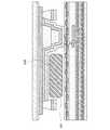
また、発光素子の一部に凸部を形成し、発光素子とそれを駆動する半導体回路を貼り合わせたときに、それらの間に空隙部ができるように配置する。その空隙部に乾燥剤を配置することができる。 Moreover, a convex part is formed in a part of the light emitting element, and when the light emitting element and a semiconductor circuit for driving the light emitting element are bonded together, the light emitting element is arranged so that a gap is formed between them. A desiccant can be placed in the gap.
また、発光素子やそれを駆動する半導体回路をフレキシブル基板上に配置することができるので、それぞれを貼り合わせても形状を変えることができる。 In addition, since the light emitting element and the semiconductor circuit for driving the light emitting element can be arranged on the flexible substrate, the shape can be changed even if they are bonded to each other.
さらに、発光素子やそれを駆動する半導体回路をフレキシブル基板上に配置しても、発光素子とそれを駆動する半導体回路との間に、応力を緩和する空間(空隙部)ができるように配置する。 Furthermore, even if the light emitting element and the semiconductor circuit for driving the light emitting element are arranged on the flexible substrate, the light emitting element and the semiconductor circuit for driving the light emitting element and the semiconductor circuit for driving the light emitting element are arranged so that a space for relaxing stress (gap) is formed. .
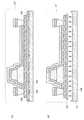
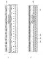
本明細書に開示される発明は、第1の電極と、前記第1の電極上の発光層と、前記発光層上に配置されかつ凸部を有する第2の電極とを有する第1のフレキシブル基板と、半導体回路と、前記半導体回路に電気的に接続される第3の電極とを有する第2のフレキシブル基板とを有し、前記第2の電極の凸部と前記第3の電極は、電気的に接続されていることを特徴とする発光装置に関する。 The invention disclosed in this specification includes a first flexible electrode including a first electrode, a light emitting layer on the first electrode, and a second electrode disposed on the light emitting layer and having a convex portion. A second flexible substrate having a substrate, a semiconductor circuit, and a third electrode electrically connected to the semiconductor circuit, wherein the convex portion of the second electrode and the third electrode are: The present invention relates to a light-emitting device that is electrically connected.
前記第1のフレキシブル基板と前記第2のフレキシブル基板とが対向配置されることによって生じた空隙部に乾燥剤が装入されていることを特徴とする発光装置に関する。 The present invention relates to a light emitting device characterized in that a desiccant is inserted into a gap formed by arranging the first flexible substrate and the second flexible substrate to face each other.
また本明細書に開示される発明は、第1の電極と、前記第1の電極上の発光層と、前記発光層上に配置されかつ凸部を有する第2の電極とを有する第1のフレキシブル基板と、半導体回路と、前記半導体回路に電気的に接続される第3の電極とを有する第2のフレキシブル基板とを有し、前記第2の電極の凸部と前記第3の電極は、導電性粒子を含む異方性導電膜により電気的に接続されていることを特徴とする発光装置に関する。 The invention disclosed in this specification includes a first electrode, a light emitting layer on the first electrode, and a second electrode disposed on the light emitting layer and having a convex portion. A second flexible substrate having a flexible substrate, a semiconductor circuit, and a third electrode electrically connected to the semiconductor circuit, wherein the convex portion of the second electrode and the third electrode are The present invention also relates to a light emitting device which is electrically connected by an anisotropic conductive film containing conductive particles.
前記半導体回路を覆って、繊維体と有機樹脂を有する構造体と、前記構造体を貫通する導電性樹脂である前記第3の電極とを有することを特徴とする発光装置に関する。 The present invention relates to a light-emitting device that covers the semiconductor circuit and includes a structure including a fibrous body and an organic resin, and the third electrode that is a conductive resin that penetrates the structure.
第1の基板上に、第1の分離層、第1の絶縁膜、第1の電極、発光層、凸部を有する第2の電極を形成し、前記第1の分離層を用いて、前記第1の基板と、前記第1の絶縁膜、前記第1の電極、前記発光層、前記第2の電極を分離し、第1のフレキシブル基板上に、第1の接着層を形成し、前記第1の接着層により、前記第1のフレキシブル基板上に、前記第1の絶縁膜、前記第1の電極、前記発光層、前記第2の電極を貼り合わせ、第2の基板上に、第2の分離層、第2の絶縁膜、半導体回路、前記半導体回路に電気的に接続される第3の電極を形成し、前記第2の分離層を用いて、前記第2の基板と、前記第2の絶縁膜、前記半導体回路、前記第3の電極を分離し、第2のフレキシブル基板上に、第2の接着層を形成し、前記第2の接着層により、前記第2のフレキシブル基板上に、前記第2の絶縁膜、前記半導体回路、前記第3の電極を貼り合わせ、前記第2の電極の凸部と前記第3の電極を、電気的に接続することを特徴とする発光装置の作製方法に関する。 On the first substrate, a first separation layer, a first insulating film, a first electrode, a light emitting layer, a second electrode having a convex portion is formed, and the first separation layer is used to Separating the first substrate from the first insulating film, the first electrode, the light emitting layer, and the second electrode, forming a first adhesive layer on the first flexible substrate, The first insulating layer, the first electrode, the light emitting layer, and the second electrode are bonded to the first flexible substrate by the first adhesive layer, and the second substrate is bonded to the second substrate. Two separation layers, a second insulating film, a semiconductor circuit, and a third electrode electrically connected to the semiconductor circuit, and using the second separation layer, the second substrate, The second insulating film, the semiconductor circuit, and the third electrode are separated, a second adhesive layer is formed on the second flexible substrate, and the second adhesive is formed. Thus, the second insulating film, the semiconductor circuit, and the third electrode are bonded to the second flexible substrate, and the convex portion of the second electrode and the third electrode are electrically connected to each other. The present invention relates to a method for manufacturing a light-emitting device.
前記第1のフレキシブル基板と前記第2のフレキシブル基板とが対向配置されることによって生じた空隙部に乾燥剤が装入されていることを特徴とする発光装置の作製方法に関する。 The present invention relates to a method for manufacturing a light-emitting device, characterized in that a desiccant is inserted into a gap formed by arranging the first flexible substrate and the second flexible substrate to face each other.
また本明細書に開示される発明は、第1の基板上に、第1の分離層、第1の絶縁膜、第1の電極、発光層、凸部を有する第2の電極を形成し、前記第1の分離層を用いて、前記第1の基板と、前記第1の絶縁膜、前記第1の電極、前記発光層、前記第2の電極を分離し、第1のフレキシブル基板上に、第1の接着層を形成し、前記第1の接着層により、前記第1のフレキシブル基板上に、前記第1の絶縁膜、前記第1の電極、前記発光層、前記第2の電極を貼り合わせ、第2の基板上に、第2の分離層、第2の絶縁膜、半導体回路、前記半導体回路に電気的に接続される第3の電極を形成し、前記第2の分離層を用いて、前記第2の基板と、前記第2の絶縁膜、前記半導体回路、前記第3の電極を分離し、第2のフレキシブル基板上に、第2の接着層を形成し、前記第2の接着層により、前記第2のフレキシブル基板上に、前記第2の絶縁膜、前記半導体回路、前記第3の電極を貼り合わせ、前記第1のフレキシブル基板と前記第2のフレキシブル基板との間に、導電性粒子を含む異方性導電性膜を形成し、前記第2の電極の凸部と前記第3の電極を、前記異方性導電膜により電気的に接続することを特徴とする発光装置の作製方法に関する。 In the invention disclosed in this specification, a first separation layer, a first insulating film, a first electrode, a light-emitting layer, and a second electrode having a convex portion are formed over a first substrate, Using the first separation layer, the first substrate, the first insulating film, the first electrode, the light emitting layer, and the second electrode are separated from each other on the first flexible substrate. The first adhesive layer is formed, and the first insulating layer, the first electrode, the light emitting layer, and the second electrode are formed on the first flexible substrate by the first adhesive layer. A second separation layer, a second insulating film, a semiconductor circuit, and a third electrode electrically connected to the semiconductor circuit are formed over the second substrate by bonding, and the second separation layer is formed And separating the second substrate, the second insulating film, the semiconductor circuit, and the third electrode, and forming a second flexible substrate on the second flexible substrate. An adhesive layer is formed, and the second insulating layer, the semiconductor circuit, and the third electrode are bonded to the second flexible substrate by the second adhesive layer, and the first flexible substrate and An anisotropic conductive film containing conductive particles is formed between the second flexible substrate and the convex portion of the second electrode and the third electrode are electrically connected by the anisotropic conductive film. The present invention relates to a method for manufacturing a light-emitting device.
前記半導体回路を覆って、繊維体と有機樹脂を有する構造体を形成し、前記第3の電極として、前記構造体を貫通する導電性樹脂を形成することを特徴とする発光装置の作製方法に関する。 A method for manufacturing a light-emitting device, wherein a structure body including a fiber body and an organic resin is formed to cover the semiconductor circuit, and a conductive resin that penetrates the structure body is formed as the third electrode. .
また本明細書に開示される発明は、第1の電極と、前記第1の電極上の発光層と、前記発光層上に配置されかつ凸部を有する第2の電極とを有する第1のフレキシブル基板と、半導体回路と、前記半導体回路に電気的に接続される第3の電極とを有する第2のフレキシブル基板と、前記第2の電極の凸部と前記第3の電極は、電気的に接続されていることを特徴とする発光装置と、前記発光装置を組み込み、長手方向と短手方向を有する筐体と、前記発光装置は、前記筐体の正面及び長手方向の上部に配置されていることを特徴とする携帯電話機に関する。 The invention disclosed in this specification includes a first electrode, a light emitting layer on the first electrode, and a second electrode disposed on the light emitting layer and having a convex portion. The second flexible substrate having a flexible substrate, a semiconductor circuit, and a third electrode electrically connected to the semiconductor circuit, the convex portion of the second electrode, and the third electrode are electrically A light-emitting device connected to the housing, a housing having the light-emitting device incorporated therein and having a longitudinal direction and a short-side direction, and the light-emitting device disposed on a front surface of the housing and an upper portion in the longitudinal direction. The present invention relates to a mobile phone.
これにより、発光素子よりも下層に半導体回路が形成されないので、段差によるカバレッジ不良の発生を抑制することができる。 Thereby, since a semiconductor circuit is not formed below the light emitting element, it is possible to suppress the occurrence of coverage failure due to a step.
また、発光素子とそれを駆動する半導体回路との間の空隙部に、乾燥剤を配置することができるので、発光層に水分が侵入するのを防ぐことができる。 Moreover, since a desiccant can be arrange | positioned in the space | gap part between a light emitting element and the semiconductor circuit which drives it, it can prevent that a water | moisture content penetrate | invades into a light emitting layer.
また、発光素子やそれを駆動する半導体回路をフレキシブル基板上に配置することができるので、それぞれを貼り合わせても形状を変えることができ、様々な形状の電子機器に組み込むことができる。 In addition, since the light-emitting element and the semiconductor circuit that drives the light-emitting element can be arranged on the flexible substrate, the shape can be changed even when the light-emitting elements are bonded to each other, and the light-emitting element and the semiconductor circuit can be incorporated into electronic devices having various shapes.
さらに、フレキシブル基板上に配置された発光素子やそれを駆動する半導体回路の間に空間(空隙部)ができるので、フレキシブル基板を曲げても応力を緩和することができる。 Furthermore, since a space (gap) is formed between the light emitting elements arranged on the flexible substrate and the semiconductor circuit that drives the light emitting element, the stress can be relieved even if the flexible substrate is bent.
以下、本明細書に開示された発明の実施の態様について、図面を参照して説明する。但し、本明細書に開示された発明は多くの異なる態様で実施することが可能であり、本明細書に開示された発明の趣旨及びその範囲から逸脱することなくその形態及び詳細を様々に変更し得ることは当業者であれば容易に理解される。従って、本実施の形態の記載内容に限定して解釈されるものではない。なお、以下に示す図面において、同一部分または同様な機能を有する部分には同一の符号を付し、その繰り返しの説明は省略する。 Hereinafter, embodiments of the invention disclosed in this specification will be described with reference to the drawings. However, the invention disclosed in this specification can be implemented in many different modes, and various changes can be made in form and details without departing from the spirit and scope of the invention disclosed in this specification. It will be readily understood by those skilled in the art. Therefore, the present invention is not construed as being limited to the description of this embodiment mode. Note that in the drawings described below, the same portions or portions having similar functions are denoted by the same reference numerals, and repetitive description thereof is omitted.
なお本明細書において、半導体回路は、半導体を利用することで機能する回路を指し、さらに半導体装置とは、半導体を利用することで機能する素子及び装置全般を指し、電子回路、液晶表示装置、発光装置等を含む電気装置およびその電気装置を搭載した電子機器をその範疇とする。 Note that in this specification, a semiconductor circuit refers to a circuit that functions by using a semiconductor, and a semiconductor device refers to all elements and devices that function by using a semiconductor, such as an electronic circuit, a liquid crystal display device, The category includes an electric device including a light-emitting device and the like and an electronic device including the electric device.
なお本明細書において、第1や第2といった序数を用いる場合があるが、便宜的に呼んでいるだけであり、積層の順番や作製工程の順番等はこれに限定されない。 Note that in this specification, ordinal numbers such as “first” and “second” are sometimes used, but they are merely called for convenience, and the order of stacking, the order of manufacturing steps, and the like are not limited thereto.
[実施の形態1]
本実施の形態では、発光装置及びその作製方法について、図1、図2(A)〜図2(C)、図3(A)〜図3(B)、図4(A)〜図4(B)、図5(A)〜図5(B)、図6(A)〜図6(C)、図7(A)〜図7(D)、図8(A)〜図8(C)、図9(A)〜図9(C)、図10(A)〜図10(B)、図11、図12、図14(A)〜図14(B)、図15、図16、図17(A)〜図17(B)、図18(A)〜図18(B)、図19、図20、図21を用いて説明する。[Embodiment 1]
In this embodiment, a light-emitting device and a manufacturing method thereof are described with reference to FIGS. 1, 2A to 2C, 3A to 3B, and 4A to 4 (a). B), FIG. 5 (A) to FIG. 5 (B), FIG. 6 (A) to FIG. 6 (C), FIG. 7 (A) to FIG. 7 (D), FIG. 8 (A) to FIG. 9 (A) to 9 (C), FIG. 10 (A) to FIG. 10 (B), FIG. 11, FIG. 12, FIG. 14 (A) to FIG. 14 (B), FIG. This will be described with reference to FIGS. 17A to 17B, FIGS. 18A to 18B, FIGS. 19, 20, and 21. FIG.
まず発光素子及びその作製方法について、図2(A)〜図2(C)、図3(A)〜図3(B)、図4(A)〜図4(B)、図5(A)〜図5(B)、図6(A)〜図6(C)を用いて説明する。 First, a light-emitting element and a manufacturing method thereof are illustrated in FIGS. 2A to 2C, FIGS. 3A to 3B, FIGS. 4A to 4B, and FIG. Description will be made with reference to FIGS. 5B and 6A to 6C.
まず、基板131上に、分離層132、下地膜102、及び、電極111を形成する(図2(A)参照)。基板131としては、ガラス基板、石英基板、半導体基板、セラミック基板等を用いればよい。 First, the
下地膜102として、酸化珪素膜、窒化珪素膜、窒素を含む酸化珪素膜、酸素を含む窒化珪素膜のうちのいずれか1つ、あるいは2つ以上の積層膜とすればよい。下地膜102は、後に形成される発光層112に水分が混入するのを防ぐ機能を有する。 As the
分離層132として、プラズマCVD法やスパッタリング法等により、タングステン(W)、モリブデン(Mo)、チタン(Ti)、タンタル(Ta)、ニオブ(Nb)、ニッケル(Ni)、コバルト(Co)、ジルコニウム(Zr)、亜鉛(Zn)、ルテニウム(Ru)、ロジウム(Rh)、パラジウム(Pd)、オスミウム(Os)、イリジウム(Ir)、珪素(Si)から選択された元素または前記元素を主成分とする合金材料若しくは化合物材料からなる層を、単層または積層して形成する。珪素を含む層の結晶構造は、非晶質、微結晶、多結晶のいずれの場合でもよい。 As the
分離層132が単層構造の場合、好ましくは、タングステン、モリブデン、タングステンとモリブデンの混合物、タングステンの酸化物、タングステンの酸化窒化物、タングステンの窒化酸化物、モリブデンの酸化物、モリブデンの酸化窒化物、モリブデンの窒化酸化物、タングステンとモリブデンの混合物の酸化物、タングステンとモリブデンの混合物の酸化窒化物、タングステンとモリブデンの混合物の窒化酸化物のいずれかを含む層を形成する。なお、タングステンとモリブデンの混合物とは、例えば、タングステンとモリブデンの合金に相当する。 In the case where the
分離層132が積層構造の場合、好ましくは、1層目として、タングステン、モリブデン、タングステンとモリブデンの混合物を含む層を形成し、2層目として、タングステンの酸化物、モリブデンの酸化物、タングステンとモリブデンの混合物の酸化物、タングステンの酸化窒化物、モリブデンの酸化窒化物、タングステンとモリブデンの混合物の酸化窒化物を形成する。このように、分離層132を積層構造とする場合、金属膜と金属酸化膜との積層構造とすることが好ましい。金属酸化膜の形成方法の一例としては、スパッタ法により直接金属酸化膜を形成する方法、基板131上に形成した金属膜の表面を熱処理または酸素雰囲気下でのプラズマ処理により当該金属膜の表面を酸化して金属酸化膜を形成する方法などが挙げられる。 In the case where the
金属膜としては、前述したタングステン(W)、モリブデン(Mo)以外に、チタン(Ti)、タンタル(Ta)、ニオブ(Nb)、ニッケル(Ni)、コバルト(Co)、ジルコニウム(Zr)、亜鉛(Zn)、ルテニウム(Ru)、ロジウム(Rh)、パラジウム(Pd)、オスミウム(Os)、イリジウム(Ir)から選択された元素または前記元素を主成分とする合金材料若しくは化合物材料からなる膜を用いることができる。 As the metal film, in addition to the above-described tungsten (W) and molybdenum (Mo), titanium (Ti), tantalum (Ta), niobium (Nb), nickel (Ni), cobalt (Co), zirconium (Zr), zinc A film made of an element selected from (Zn), ruthenium (Ru), rhodium (Rh), palladium (Pd), osmium (Os), iridium (Ir), or an alloy material or a compound material containing the element as a main component. Can be used.
なお、分離層132を形成する前に、基板131上に酸化珪素膜、窒化珪素膜、窒素を含む酸化珪素膜、酸素を含む窒化珪素膜などの絶縁膜を形成し、当該絶縁膜上に分離層132を形成するようにしてもよい。基板131と分離層132との間にこのような絶縁膜を設けることにより、基板131が含む不純物が上層に侵入してしまうことを防止することができる。また、後にレーザを照射する工程があるが、その工程の際、基板131がエッチングされてしまうことを防止することができる。なお、ここで、窒素を含む酸化珪素膜と、酸素を含む窒化珪素膜とでは、前者は窒素よりも酸素を多く含み、後者は酸素よりも窒素を多く含むという意味で使い分けている。 Note that before the
電極111は、透光性を有する導電膜を用いて形成すればよい。透光性を有する導電膜の材料は、酸化インジウム(In2O3)や酸化インジウム酸化スズ合金(In2O3―SnO2;Indium Tin Oxide(ITO))などをスパッタ法や真空蒸着法などを用いて形成して用いることができる。酸化インジウム酸化亜鉛合金(In2O3―ZnO)を用いても良い。また、酸化亜鉛(ZnO)も適した材料であり、さらに可視光の透過率や導電率を高めるためにガリウム(Ga)を添加した酸化亜鉛(ZnO:Ga)などを用いることができる。このような材料を用いて電極111を形成した場合、電極111は陽極となる。The
電極111を陰極とする場合には、アルミニウムなど仕事関数の低い材料の極薄膜を用いるか、そのような物質の薄膜と上述のような透光性を有する導電膜との積層構造を用いることによって作製することができる。 In the case where the
次いで、下地膜102及び電極111を覆って、絶縁膜121を形成する(図2(B)参照)。絶縁膜121は、絶縁膜121には、無機材料や有機材料を用いることができる。 Next, an insulating
無機材料として、例えば、酸化珪素、窒化珪素、窒素を含む酸化珪素、ダイヤモンド状炭素(Diamond Like Carbon(DLC))のいずれか1つ、あるいは、2つ以上の積層構造を用いることができる。また、有機材料として、ポリイミド、アクリル、ポリアミド、ポリイミドアミド、レジストまたはベンゾシクロブテン、シロキサンのうちいずれか1つ、あるいは、2つ以上の積層構造を用いればよい。 As the inorganic material, for example, any one of silicon oxide, silicon nitride, silicon oxide containing nitrogen, and diamond-like carbon (DLC), or a stacked structure of two or more can be used. As the organic material, any one of polyimide, acrylic, polyamide, polyimide amide, resist, benzocyclobutene, and siloxane, or a stacked structure of two or more may be used.
シロキサンとは、珪素(Si)と酸素(O)との結合で骨格構造が構成され、置換基に少なくとも水素を含む、あるいは、置換基にフッ素、アルキル基、または芳香族炭化水素のうち少なくとも1種を有するポリマー材料を出発原料として形成される。また、置換基としてフルオロ基を用いてもよく、さらに置換基として、少なくとも水素を含む有機基及びフルオロ基とを用いてもよい。 Siloxane has a skeletal structure composed of a bond of silicon (Si) and oxygen (O) and contains at least hydrogen as a substituent, or at least one of fluorine, an alkyl group, and aromatic hydrocarbon as a substituent. A polymer material having a seed is formed as a starting material. Further, a fluoro group may be used as a substituent, and an organic group containing at least hydrogen and a fluoro group may be used as a substituent.
次いで絶縁膜121を用いて、スペーサ105、隔壁104a、隔壁104bを形成する(図2(C)参照)。このとき、スペーサ105は順テーパ型、すなわち断面形状が、上底が下底より短い台形になるように形成する。また、隔壁104a及び隔壁104bはそれぞれ、逆テーパ型、すなわち断面形状が、上底が下底より長い台形になるように形成する。 Next, the
さらにスペーサ105の断面形状は、後に形成される発光層112及び電極113の被覆率が向上するように、台形の四隅が曲率半径を有する形状にしてもよい。 Furthermore, the cross-sectional shape of the
隔壁104a及び隔壁104bはそれぞれ、後に形成される発光層112及び電極113を、画素ごとに分離する機能を有する。 Each of the
なお絶縁膜121を形成せずに、スペーサ105、隔壁104a、隔壁104bを、絶縁物を用いて始めからそれぞれの形状に形成してもよい。例えば、インクジェット法等で、はじめから逆テーパ型に形成してもよい。 Note that without forming the insulating
次いで、絶縁膜121の説明で挙げた材料いずれかを用い、下地膜102、電極111、スペーサ105、隔壁104a、隔壁104bを覆って、絶縁膜138を形成する(図3(A)参照)。あるいは、絶縁膜138は、絶縁膜121とは別の材料を用いて形成してもよい。 Next, the insulating
絶縁膜138を用いて、スペーサ105上に、スペーサ106を形成する(図3(B)参照)。スペーサ106は順テーパ型、すなわち断面形状が、上底が下底より短い台形になるように形成する。 A
なお絶縁膜138を形成せずに、スペーサ106を、絶縁物を用いて始めからその形状に形成してもよい。例えば、インクジェット法等で、はじめから順テーパ型に形成してもよい。 Note that without forming the insulating
スペーサ106の断面形状は、後に形成される発光層112及び電極113の被覆率が向上するように、台形の四隅が曲率半径を有する形状にしてもよい。 The cross-sectional shape of the
スペーサ105及びスペーサ106を形成することにより、後に形成される発光層112及び電極113が、スペーサ105及びスペーサ106に沿って持ち上がることになる。すなわち、発光層112及び電極113に凸部が生じ、電極113の凸部と、後述するTFT211に電気的に接続される導電性樹脂306が、電気的に接続される。電極113の凸部及び導電性樹脂306が、電極113、発光層112、TFT211と離れた位置で接続されるので、電極113、発光層112、TFT211にダメージを与えるのを防ぐことができる。 By forming the
次いで、電極111上のうち隔壁104a及び隔壁104bで囲まれた領域に、発光層112及び電極113を形成する(図4(A)参照)。なお、隔壁104a上に発光層112と同じ材料からなるEL材料層107a及び電極113と同じ材料からなる導電材料層108a、並びに、隔壁104b上には発光層112と同じ材料からなるEL材料層107b及び電極113と同じ材料からなる導電材料層108bが形成されるが、それぞれ絶縁膜からなる隔壁104a及び隔壁104bにより、電極111とは電気的に絶縁されているため発光しない。 Next, the light-emitting
発光層112は、単層であってもよいし、発光層と電極111との間、あるいは、発光層と電極113との間に、電子及び正孔両キャリアの注入、移動、あるいは、再結合を行わせるための層、すなわちキャリア輸送層やキャリア注入層等を自由に組み合わせることが可能である。また、発光層112は、発光層単層である場合、あるいは、発光層及びキャリア輸送層やキャリア注入層等を組み合わせた積層構造である場合も、合わせて発光層112と呼ぶものとする。 The
以下に、正孔注入層、正孔輸送層、発光層、電子輸送層、電子注入層を構成する材料について具体的に説明する。 Below, the material which comprises a positive hole injection layer, a positive hole transport layer, a light emitting layer, an electron carrying layer, and an electron injection layer is demonstrated concretely.
正孔注入層は、電極111または電極113の一方である陽極に接して設けられ、正孔注入性の高い物質を含む層である。モリブデン酸化物やバナジウム酸化物、ルテニウム酸化物、タングステン酸化物、マンガン酸化物等を用いることができる。この他、フタロシアニン(略称:H2Pc)や銅フタロシアニン(CuPC)等のフタロシアニン系の化合物、4,4’−ビス[N−(4−ジフェニルアミノフェニル)−N−フェニルアミノ]ビフェニル(略称:DPAB)、4,4’−ビス(N−{4−[N−(3−メチルフェニル)−N−フェニルアミノ]フェニル}−N−フェニルアミノ)ビフェニル(略称:DNTPD)等の芳香族アミン化合物、或いはポリ(エチレンジオキシチオフェン)/ポリ(スチレンスルホン酸)(PEDOT/PSS)等の高分子等によっても正孔注入層を形成することができる。The hole injection layer is a layer that is provided in contact with the anode which is one of the
また、正孔注入層として、正孔輸送性の高い物質にアクセプター性物質を含有させた複合材料を用いることができる。なお、正孔輸送性の高い物質にアクセプター性物質を含有させたものを用いることにより、電極の仕事関数に依らず電極を形成する材料を選ぶことができる。つまり、陽極として仕事関数の大きい材料だけでなく、仕事関数の小さい材料を用いることができる。アクセプター性物質としては、7,7,8,8−テトラシアノ−2,3,5,6−テトラフルオロキノジメタン(略称:F4−TCNQ)、クロラニル等を挙げることができる。また、遷移金属酸化物を挙げることができる。また元素周期表における第4族乃至第8族に属する金属の酸化物を挙げることができる。具体的には、酸化バナジウム、酸化ニオブ、酸化タンタル、酸化クロム、酸化モリブデン、酸化タングステン、酸化マンガン、酸化レニウムは電子受容性が高いため好ましい。中でも特に、酸化モリブデンは大気中でも安定であり、吸湿性が低く、扱いやすいため好ましい。For the hole injection layer, a composite material in which an acceptor substance is contained in a substance having a high hole-transport property can be used. Note that by using a substance having an acceptor substance contained in a substance having a high hole-transport property, a material for forming an electrode can be selected regardless of the work function of the electrode. That is, not only a material having a high work function but also a material having a low work function can be used as the anode. As the acceptor substance, 7,7,8,8-tetracyano-2,3,5,6-tetrafluoroquinodimethane (abbreviation: F4 -TCNQ), chloranil, and the like can be given. Moreover, a transition metal oxide can be mentioned. In addition, oxides of metals belonging to
複合材料に用いる正孔輸送性の高い物質としては、芳香族アミン化合物、カルバゾール誘導体、芳香族炭化水素、高分子化合物(オリゴマー、デンドリマー、ポリマー等)など、種々の化合物を用いることができる。なお、複合材料に用いる有機化合物としては、正孔輸送性の高い有機化合物であることが好ましい。具体的には、10−6cm2/Vs以上の正孔移動度を有する物質であることが好ましい。但し、電子よりも正孔の輸送性の高い物質であれば、これら以外のものを用いてもよい。以下では、複合材料に用いることのできる有機化合物を具体的に列挙する。As the substance having a high hole-transport property used for the composite material, various compounds such as an aromatic amine compound, a carbazole derivative, an aromatic hydrocarbon, and a high molecular compound (oligomer, dendrimer, polymer, and the like) can be used. Note that the organic compound used for the composite material is preferably an organic compound having a high hole-transport property. Specifically, a substance having a hole mobility of 10−6 cm2 / Vs or higher is preferable. Note that other than these substances, any substance that has a property of transporting more holes than electrons may be used. Below, the organic compound which can be used for a composite material is listed concretely.
例えば、芳香族アミン化合物としては、N,N’−ジ(p−トリル)−N,N’−ジフェニル−p−フェニレンジアミン(略称:DTDPPA)、4,4’−ビス[N−(4−ジフェニルアミノフェニル)−N−フェニルアミノ]ビフェニル(略称:DPAB)、4,4’−ビス(N−{4−[N−(3−メチルフェニル)−N−フェニルアミノ]フェニル}−N−フェニルアミノ)ビフェニル(略称:DNTPD)、1,3,5−トリス[N−(4−ジフェニルアミノフェニル)−N−フェニルアミノ]ベンゼン(略称:DPA3B)等を挙げることができる。 For example, as an aromatic amine compound, N, N′-di (p-tolyl) -N, N′-diphenyl-p-phenylenediamine (abbreviation: DTDPPA), 4,4′-bis [N- (4- Diphenylaminophenyl) -N-phenylamino] biphenyl (abbreviation: DPAB), 4,4′-bis (N- {4- [N- (3-methylphenyl) -N-phenylamino] phenyl} -N-phenyl Amino) biphenyl (abbreviation: DNTPD), 1,3,5-tris [N- (4-diphenylaminophenyl) -N-phenylamino] benzene (abbreviation: DPA3B), and the like can be given.
複合材料に用いることのできるカルバゾール誘導体としては、具体的には、3−[N−(9−フェニルカルバゾール−3−イル)−N−フェニルアミノ]−9−フェニルカルバゾール(略称:PCzPCA1)、3,6−ビス[N−(9−フェニルカルバゾール−3−イル)−N−フェニルアミノ]−9−フェニルカルバゾール(略称:PCzPCA2)、3−[N−(1−ナフチル)−N−(9−フェニルカルバゾール−3−イル)アミノ]−9−フェニルカルバゾール(略称:PCzPCN1)等を挙げることができる。 Specific examples of the carbazole derivative that can be used for the composite material include 3- [N- (9-phenylcarbazol-3-yl) -N-phenylamino] -9-phenylcarbazole (abbreviation: PCzPCA1), 3 , 6-Bis [N- (9-phenylcarbazol-3-yl) -N-phenylamino] -9-phenylcarbazole (abbreviation: PCzPCA2), 3- [N- (1-naphthyl) -N- (9- Phenylcarbazol-3-yl) amino] -9-phenylcarbazole (abbreviation: PCzPCN1) and the like.
また、複合材料に用いることのできるカルバゾール誘導体としては、他に、4,4’−ジ(N−カルバゾリル)ビフェニル(略称:CBP)、1,3,5−トリス[4−(N−カルバゾリル)フェニル]ベンゼン(略称:TCPB)、9−[4−(10−フェニル−9−アントリル)フェニル]−9H−カルバゾール(略称:CzPA)、1,4−ビス[4−(N−カルバゾリル)フェニル]−2,3,5,6−テトラフェニルベンゼン等を用いることができる。 As other carbazole derivatives that can be used for the composite material, 4,4′-di (N-carbazolyl) biphenyl (abbreviation: CBP), 1,3,5-tris [4- (N-carbazolyl) Phenyl] benzene (abbreviation: TCPB), 9- [4- (10-phenyl-9-anthryl) phenyl] -9H-carbazole (abbreviation: CzPA), 1,4-bis [4- (N-carbazolyl) phenyl] -2,3,5,6-tetraphenylbenzene and the like can be used.
また、複合材料に用いることのできる芳香族炭化水素としては、例えば、2−tert−ブチル−9,10−ジ(2−ナフチル)アントラセン(略称:t−BuDNA)、2−tert−ブチル−9,10−ジ(1−ナフチル)アントラセン、9,10−ビス(3,5−ジフェニルフェニル)アントラセン(略称:DPPA)、2−tert−ブチル−9,10−ビス(4−フェニルフェニル)アントラセン(略称:t−BuDBA)、9,10−ジ(2−ナフチル)アントラセン(略称:DNA)、9,10−ジフェニルアントラセン(略称:DPAnth)、2−tert−ブチルアントラセン(略称:t−BuAnth)、9,10−ビス(4−メチル−1−ナフチル)アントラセン(略称:DMNA)、2−tert−ブチル−9,10−ビス[2−(1−ナフチル)フェニル]アントラセン、9,10−ビス[2−(1−ナフチル)フェニル]アントラセン、2,3,6,7−テトラメチル−9,10−ジ(1−ナフチル)アントラセン、2,3,6,7−テトラメチル−9,10−ジ(2−ナフチル)アントラセン、9,9’−ビアントリル、10,10’−ジフェニル−9,9’−ビアントリル、10,10’−ビス(2−フェニルフェニル)−9,9’−ビアントリル、10,10’−ビス[(2,3,4,5,6−ペンタフェニル)フェニル]−9,9’−ビアントリル、アントラセン、テトラセン、ルブレン、ペリレン、2,5,8,11−テトラ(tert−ブチル)ペリレン等が挙げられる。また、この他、ペンタセン、コロネン等も用いることができる。このように、1×10−6cm2/Vs以上の正孔移動度を有し、炭素数14〜42である芳香族炭化水素を用いることがより好ましい。Examples of aromatic hydrocarbons that can be used for the composite material include 2-tert-butyl-9,10-di (2-naphthyl) anthracene (abbreviation: t-BuDNA), 2-tert-butyl-9. , 10-di (1-naphthyl) anthracene, 9,10-bis (3,5-diphenylphenyl) anthracene (abbreviation: DPPA), 2-tert-butyl-9,10-bis (4-phenylphenyl) anthracene ( Abbreviations: t-BuDBA), 9,10-di (2-naphthyl) anthracene (abbreviation: DNA), 9,10-diphenylanthracene (abbreviation: DPAnth), 2-tert-butylanthracene (abbreviation: t-BuAnth), 9,10-bis (4-methyl-1-naphthyl) anthracene (abbreviation: DMNA), 2-tert-butyl-9, 0-bis [2- (1-naphthyl) phenyl] anthracene, 9,10-bis [2- (1-naphthyl) phenyl] anthracene, 2,3,6,7-tetramethyl-9,10-di (1 -Naphthyl) anthracene, 2,3,6,7-tetramethyl-9,10-di (2-naphthyl) anthracene, 9,9'-bianthryl, 10,10'-diphenyl-9,9'-bianthryl, 10 , 10′-bis (2-phenylphenyl) -9,9′-bianthryl, 10,10′-bis [(2,3,4,5,6-pentaphenyl) phenyl] -9,9′-bianthryl, Anthracene, tetracene, rubrene, perylene, 2,5,8,11-tetra (tert-butyl) perylene and the like can be mentioned. In addition, pentacene, coronene, and the like can also be used. Thus, it is more preferable to use an aromatic hydrocarbon having a hole mobility of 1 × 10⁻⁶ cm2 / Vs or more and having 14 to 42 carbon atoms.
なお、複合材料に用いることのできる芳香族炭化水素は、ビニル骨格を有していてもよい。ビニル基を有している芳香族炭化水素としては、例えば、4,4’−ビス(2,2−ジフェニルビニル)ビフェニル(略称:DPVBi)、9,10−ビス[4−(2,2−ジフェニルビニル)フェニル]アントラセン(略称:DPVPA)等が挙げられる。 Note that the aromatic hydrocarbon that can be used for the composite material may have a vinyl skeleton. As the aromatic hydrocarbon having a vinyl group, for example, 4,4′-bis (2,2-diphenylvinyl) biphenyl (abbreviation: DPVBi), 9,10-bis [4- (2,2- Diphenylvinyl) phenyl] anthracene (abbreviation: DPVPA) and the like.
また、ポリ(N−ビニルカルバゾール)(略称:PVK)やポリ(4−ビニルトリフェニルアミン)(略称:PVTPA)、ポリ[N−(4−{N’−[4−(4−ジフェニルアミノ)フェニル]フェニル−N’−フェニルアミノ}フェニル)メタクリルアミド](略称:PTPDMA)ポリ[N,N’−ビス(4−ブチルフェニル)−N,N’−ビス(フェニル)ベンジジン](略称:Poly−TPD)等の高分子化合物を用いることもできる。 In addition, poly (N-vinylcarbazole) (abbreviation: PVK), poly (4-vinyltriphenylamine) (abbreviation: PVTPA), poly [N- (4- {N ′-[4- (4-diphenylamino)] Phenyl] phenyl-N′-phenylamino} phenyl) methacrylamide] (abbreviation: PTPDMA) poly [N, N′-bis (4-butylphenyl) -N, N′-bis (phenyl) benzidine] (abbreviation: Poly High molecular compounds such as -TPD) can also be used.
正孔輸送層は、正孔輸送性の高い物質を含む層である。正孔輸送性の高い物質としては、例えば、4,4’−ビス[N−(1−ナフチル)−N−フェニルアミノ]ビフェニル(略称:NPB)やN,N’−ビス(3−メチルフェニル)−N,N’−ジフェニル−[1,1’−ビフェニル]−4,4’−ジアミン(略称:TPD)、4,4’,4’’−トリス(N,N−ジフェニルアミノ)トリフェニルアミン(略称:TDATA)、4,4’,4’’−トリス[N−(3−メチルフェニル)−N−フェニルアミノ]トリフェニルアミン(略称:MTDATA)、4,4’−ビス[N−(スピロ−9,9’−ビフルオレン−2−イル)−N―フェニルアミノ]ビフェニル(略称:BSPB)などの芳香族アミン化合物等を用いることができる。ここに述べた物質は、主に10−6cm2/Vs以上の正孔移動度を有する物質である。但し、電子よりも正孔の輸送性の高い物質であれば、これら以外のものを用いてもよい。なお、正孔輸送性の高い物質を含む層は、単層のものだけでなく、上記物質からなる層が二層以上積層したものとしてもよい。The hole transport layer is a layer containing a substance having a high hole transport property. Examples of the substance having a high hole-transport property include 4,4′-bis [N- (1-naphthyl) -N-phenylamino] biphenyl (abbreviation: NPB) and N, N′-bis (3-methylphenyl). ) -N, N′-diphenyl- [1,1′-biphenyl] -4,4′-diamine (abbreviation: TPD), 4,4 ′, 4 ″ -tris (N, N-diphenylamino) triphenyl Amine (abbreviation: TDATA), 4,4 ′, 4 ″ -tris [N- (3-methylphenyl) -N-phenylamino] triphenylamine (abbreviation: MTDATA), 4,4′-bis [N— An aromatic amine compound such as (spiro-9,9′-bifluoren-2-yl) -N-phenylamino] biphenyl (abbreviation: BSPB) can be used. The substances described here are mainly substances having a hole mobility of 10−6 cm2 / Vs or higher. Note that other than these substances, any substance that has a property of transporting more holes than electrons may be used. Note that the layer containing a substance having a high hole-transport property is not limited to a single layer, and two or more layers containing the above substances may be stacked.
また、正孔輸送層として、ポリ(N−ビニルカルバゾール)(略称:PVK)やポリ(4−ビニルトリフェニルアミン)(略称:PVTPA)等の高分子化合物を用いることもできる。 Alternatively, a high molecular compound such as poly (N-vinylcarbazole) (abbreviation: PVK) or poly (4-vinyltriphenylamine) (abbreviation: PVTPA) can be used for the hole-transporting layer.
発光層は、発光性の物質を含む層である。発光層の種類としては、発光中心物質を主成分とするいわゆる単膜の発光層であっても、ホスト材料中に発光中心材料を分散するいわゆるホスト−ゲスト型の発光層であってもどちらでも構わない。 The light emitting layer is a layer containing a light emitting substance. The type of the light-emitting layer may be a so-called single-layer light-emitting layer mainly composed of an emission center material, or a so-called host-guest type light-emitting layer in which the emission center material is dispersed in the host material. I do not care.
用いられる発光中心材料に制限は無く、公知の蛍光または燐光を発する材料を用いることができる。蛍光発光性材料としては、例えばN,N’−ビス[4−(9H−カルバゾール−9−イル)フェニル]−N,N’−ジフェニルスチルベン−4,4’−ジアミン(略称:YGA2S)、4−(9H−カルバゾール−9−イル)−4’−(10−フェニル−9−アントリル)トリフェニルアミン(略称:YGAPA)、等の他、発光波長が450nm以上の4−(9H−カルバゾール−9−イル)−4’−(9,10−ジフェニル−2−アントリル)トリフェニルアミン(略称:2YGAPPA)、N,9−ジフェニル−N−[4−(10−フェニル−9−アントリル)フェニル]−9H−カルバゾール−3−アミン(略称:PCAPA)、ペリレン、2,5,8,11−テトラ−tert−ブチルペリレン(略称:TBP)、4−(10−フェニル−9−アントリル)−4’−(9−フェニル−9H−カルバゾール−3−イル)トリフェニルアミン(略称:PCBAPA)、N,N’’−(2−tert−ブチルアントラセン−9,10−ジイルジ−4,1−フェニレン)ビス[N,N’,N’−トリフェニル−1,4−フェニレンジアミン](略称:DPABPA)、N,9−ジフェニル−N−[4−(9,10−ジフェニル−2−アントリル)フェニル]−9H−カルバゾール−3−アミン(略称:2PCAPPA)、N−[4−(9,10−ジフェニル−2−アントリル)フェニル]−N,N’,N’−トリフェニル−1,4−フェニレンジアミン(略称:2DPAPPA)、N,N,N’,N’,N’’,N’’,N’’’,N’’’−オクタフェニルジベンゾ[g,p]クリセン−2,7,10,15−テトラアミン(略称:DBC1)、クマリン30、N−(9,10−ジフェニル−2−アントリル)−N,9−ジフェニル−9H−カルバゾール−3−アミン(略称:2PCAPA)、N−[9,10−ビス(1,1’−ビフェニル−2−イル)−2−アントリル]−N,9−ジフェニル−9H−カルバゾール−3−アミン(略称:2PCABPhA)、N−(9,10−ジフェニル−2−アントリル)−N,N’,N’−トリフェニル−1,4−フェニレンジアミン(略称:2DPAPA)、N−[9,10−ビス(1,1’−ビフェニル−2−イル)−2−アントリル]−N,N’,N’−トリフェニル−1,4−フェニレンジアミン(略称:2DPABPhA)、9,10−ビス(1,1’−ビフェニル−2−イル)−N−[4−(9H−カルバゾール−9−イル)フェニル]−N−フェニルアントラセン−2−アミン(略称:2YGABPhA)、N,N,9−トリフェニルアントラセン−9−アミン(略称:DPhAPhA)クマリン545T、N,N’−ジフェニルキナクリドン、(略称:DPQd)、ルブレン、5,12−ビス(1,1’−ビフェニル−4−イル)−6,11−ジフェニルテトラセン(略称:BPT)、2−(2−{2−[4−(ジメチルアミノ)フェニル]エテニル}−6−メチル−4H−ピラン−4−イリデン)プロパンジニトリル(略称:DCM1)、2−{2−メチル−6−[2−(2,3,6,7−テトラヒドロ−1H,5H−ベンゾ[ij]キノリジン−9−イル)エテニル]−4H−ピラン−4−イリデン}プロパンジニトリル(略称:DCM2)、N,N,N’,N’−テトラキス(4−メチルフェニル)テトラセン−5,11−ジアミン(略称:p−mPhTD)、7,13−ジフェニル−N,N,N’,N’−テトラキス(4−メチルフェニル)アセナフト[1,2−a]フルオランテン−3,10−ジアミン(略称:p−mPhAFD)、2−{2−イソプロピル−6−[2−(1,1,7,7−テトラメチル−2,3,6,7−テトラヒドロ−1H,5H−ベンゾ[ij]キノリジン−9−イル)エテニル]−4H−ピラン−4−イリデン}プロパンジニトリル(略称:DCJTI)、2−{2−tert−ブチル−6−[2−(1,1,7,7−テトラメチル−2,3,6,7−テトラヒドロ−1H,5H−ベンゾ[ij]キノリジン−9−イル)エテニル]−4H−ピラン−4−イリデン}プロパンジニトリル(略称:DCJTB)、2−(2,6−ビス{2−[4−(ジメチルアミノ)フェニル]エテニル}−4H−ピラン−4−イリデン)プロパンジニトリル(略称:BisDCM)、2−{2,6−ビス[2−(8−メトキシ−1,1,7,7−テトラメチル−2,3,6,7−テトラヒドロ−1H,5H−ベンゾ[ij]キノリジン−9−イル)エテニル]−4H−ピラン−4−イリデン}プロパンジニトリル(略称:BisDCJTM)などが挙げられる。燐光発光性材料としては、例えば、ビス[2−(4’,6’−ジフルオロフェニル)ピリジナト−N,C2’]イリジウム(III)テトラキス(1−ピラゾリル)ボラート(略称:FIr6)、の他、発光波長が470nm〜500nmの範囲にある、ビス[2−(4’,6’−ジフルオロフェニル)ピリジナト−N,C2’]イリジウム(III)ピコリナート(略称:FIrpic)、ビス[2−(3’,5’−ビストリフルオロメチルフェニル)ピリジナト−N,C2’]イリジウム(III)ピコリナート(略称:Ir(CF3ppy)2(pic))、ビス[2−(4’,6’−ジフルオロフェニル)ピリジナト−N,C2’]イリジウム(III)アセチルアセトナート(略称:FIracac)、発光波長が500nm(緑色発光)以上のトリス(2−フェニルピリジナト)イリジウム(III)(略称:Ir(ppy)3)、ビス(2−フェニルピリジナト)イリジウム(III)アセチルアセトナート(略称:Ir(ppy)2(acac))、トリス(アセチルアセトナト)(モノフェナントロリン)テルビウム(III)(略称:Tb(acac)3(Phen))、ビス(ベンゾ[h]キノリナト)イリジウム(III)アセチルアセトナート(略称:Ir(bzq)2(acac))、ビス(2,4−ジフェニル−1,3−オキサゾラト−N,C2’)イリジウム(III)アセチルアセトナート(略称:Ir(dpo)2(acac))、ビス[2−(4’−パーフルオロフェニルフェニル)ピリジナト]イリジウム(III)アセチルアセトナート(略称:Ir(p−PF−ph)2(acac))、ビス(2−フェニルベンゾチアゾラト−N,C2’)イリジウム(III)アセチルアセトナート(略称:Ir(bt)2(acac))、ビス[2−(2’−ベンゾ[4,5−α]チエニル)ピリジナト−N,C3’]イリジウム(III)アセチルアセトナート(略称:Ir(btp)2(acac))、ビス(1−フェニルイソキノリナト−N,C2’)イリジウム(III)アセチルアセトナート(略称:Ir(piq)2(acac))、(アセチルアセトナト)ビス[2,3−ビス(4−フルオロフェニル)キノキサリナト]イリジウム(III)(略称:Ir(Fdpq)2(acac))、(アセチルアセトナト)ビス(2,3,5−トリフェニルピラジナト)イリジウム(III)(略称:Ir(tppr)2(acac))、2,3,7,8,12,13,17,18−オクタエチル−21H,23H−ポルフィリン白金(II)(略称:PtOEP)、トリス(1,3−ジフェニル−1,3−プロパンジオナト)(モノフェナントロリン)ユーロピウム(III)(略称:Eu(DBM)3(Phen))、トリス[1−(2−テノイル)−3,3,3−トリフルオロアセトナト](モノフェナントロリン)ユーロピウム(III)(略称:Eu(TTA)3(Phen))等が挙げられる。以上のような材料または他の公知の材料の中から、各々の発光素子における発光色を考慮し選択すれば良い。There is no restriction | limiting in the luminescent center material used, The material which emits well-known fluorescence or phosphorescence can be used. As a fluorescent material, for example, N, N′-bis [4- (9H-carbazol-9-yl) phenyl] -N, N′-diphenylstilbene-4,4′-diamine (abbreviation: YGA2S), 4 -(9H-carbazol-9-yl) -4 '-(10-phenyl-9-anthryl) triphenylamine (abbreviation: YGAPA), etc., and 4- (9H-carbazole-9 having an emission wavelength of 450 nm or more -Yl) -4 '-(9,10-diphenyl-2-anthryl) triphenylamine (abbreviation: 2YGAPPA), N, 9-diphenyl-N- [4- (10-phenyl-9-anthryl) phenyl]- 9H-carbazol-3-amine (abbreviation: PCAPA), perylene, 2,5,8,11-tetra-tert-butylperylene (abbreviation: TBP), 4- (10-phenyl) 9-anthryl) -4 ′-(9-phenyl-9H-carbazol-3-yl) triphenylamine (abbreviation: PCBAPA), N, N ″-(2-tert-butylanthracene-9,10-diyldi- 4,1-phenylene) bis [N, N ′, N′-triphenyl-1,4-phenylenediamine] (abbreviation: DPABPA), N, 9-diphenyl-N- [4- (9,10-diphenyl-) 2-anthryl) phenyl] -9H-carbazol-3-amine (abbreviation: 2PCAPPA), N- [4- (9,10-diphenyl-2-anthryl) phenyl] -N, N ′, N′-triphenyl- 1,4-phenylenediamine (abbreviation: 2DPAPPA), N, N, N ′, N ′, N ″, N ″, N ′ ″, N ′ ″-octaphenyldibenzo [g, p] chrysene- 2,7,10,15-te Laamine (abbreviation: DBC1), Coumarin 30, N- (9,10-diphenyl-2-anthryl) -N, 9-diphenyl-9H-carbazol-3-amine (abbreviation: 2PCAPA), N- [9,10- Bis (1,1′-biphenyl-2-yl) -2-anthryl] -N, 9-diphenyl-9H-carbazol-3-amine (abbreviation: 2PCABPhA), N- (9,10-diphenyl-2-anthryl) ) -N, N ′, N′-triphenyl-1,4-phenylenediamine (abbreviation: 2DPAPA), N- [9,10-bis (1,1′-biphenyl-2-yl) -2-anthryl] -N, N ', N'-triphenyl-1,4-phenylenediamine (abbreviation: 2DPABPhA), 9,10-bis (1,1'-biphenyl-2-yl) -N- [4- (9H- Carbazo Ru-9-yl) phenyl] -N-phenylanthracen-2-amine (abbreviation: 2YGABPhA), N, N, 9-triphenylanthracen-9-amine (abbreviation: DPhAPhA) coumarin 545T, N, N′-diphenyl Quinacridone, (abbreviation: DPQd), rubrene, 5,12-bis (1,1′-biphenyl-4-yl) -6,11-diphenyltetracene (abbreviation: BPT), 2- (2- {2- [4 -(Dimethylamino) phenyl] ethenyl} -6-methyl-4H-pyran-4-ylidene) propanedinitrile (abbreviation: DCM1), 2- {2-methyl-6- [2- (2,3,6,6) 7-tetrahydro-1H, 5H-benzo [ij] quinolizin-9-yl) ethenyl] -4H-pyran-4-ylidene} propanedinitrile (abbreviation: DCM2), , N, N ′, N′-tetrakis (4-methylphenyl) tetracene-5,11-diamine (abbreviation: p-mPhTD), 7,13-diphenyl-N, N, N ′, N′-tetrakis (4 -Methylphenyl) acenaphtho [1,2-a] fluoranthene-3,10-diamine (abbreviation: p-mPhAFD), 2- {2-isopropyl-6- [2- (1,1,7,7-tetramethyl) -2,3,6,7-tetrahydro-1H, 5H-benzo [ij] quinolizin-9-yl) ethenyl] -4H-pyran-4-ylidene} propanedinitrile (abbreviation: DCJTI), 2- {2- tert-Butyl-6- [2- (1,1,7,7-tetramethyl-2,3,6,7-tetrahydro-1H, 5H-benzo [ij] quinolizin-9-yl) ethenyl] -4H- Piran-4-i Den} propanedinitrile (abbreviation: DCJTB), 2- (2,6-bis {2- [4- (dimethylamino) phenyl] ethenyl} -4H-pyran-4-ylidene) propanedinitrile (abbreviation: BisDCM) 2- {2,6-bis [2- (8-methoxy-1,1,7,7-tetramethyl-2,3,6,7-tetrahydro-1H, 5H-benzo [ij] quinolidine-9- Yl) ethenyl] -4H-pyran-4-ylidene} propanedinitrile (abbreviation: BisDCJTM). Examples of the phosphorescent material include bis [2- (4 ′, 6′-difluorophenyl) pyridinato-N, C2 ′ ] iridium (III) tetrakis (1-pyrazolyl) borate (abbreviation: FIr6), and the like. , Bis [2- (4 ′, 6′-difluorophenyl) pyridinato-N, C2 ′ ] iridium (III) picolinate (abbreviation: FIrpic), bis [2- () having an emission wavelength in the range of 470 nm to 500 nm. 3 ′, 5′-bistrifluoromethylphenyl) pyridinato-N, C2 ′ ] iridium (III) picolinate (abbreviation: Ir (CF3 ppy)2 (pic)), bis [2- (4 ′, 6′- difluorophenyl) pyridinato -N, C2 '] iridium (III) acetylacetonate (abbreviation: FIracac), emission wavelength 500 nm (green emission) Tris upper (2-phenylpyridinato) iridium (III) (abbreviation: Ir(ppy) 3), bis (2-phenylpyridinato) iridium (III) acetylacetonate (abbreviation: Ir(ppy) 2 ( acac)), tris (acetylacetonato) (monophenanthroline) terbium (III) (abbreviation: Tb (acac)3 (Phen)), bis (benzo [h] quinolinato) iridium (III) acetylacetonate (abbreviation: Ir (Bzq)2 (acac)), bis (2,4-diphenyl-1,3-oxazolate-N, C2 ′ ) iridium (III) acetylacetonate (abbreviation: Ir (dpo)2 (acac)), bis [2- (4′-perfluorophenylphenyl) pyridinato] iridium (III) acetylacetonate ( Abbreviations: Ir (p-PF-ph)2 (acac)), bis (2-phenylbenzothiazolate-N, C2 ′ ) iridium (III) acetylacetonate (abbreviation: Ir (bt)2 (acac) ), Bis [2- (2′-benzo [4,5-α] thienyl) pyridinato-N, C3 ′ ] iridium (III) acetylacetonate (abbreviation: Ir (btp)2 (acac)), bis ( 1-phenylisoquinolinato-N, C2 ′ ) iridium (III) acetylacetonate (abbreviation: Ir (piq)2 (acac)), (acetylacetonato) bis [2,3-bis (4-fluorophenyl) ) Quinoxalinato] iridium (III) (abbreviation: Ir (Fdpq)2 (acac)), (acetylacetonato) bis (2,3,5-triphenylpyrazinato) irid Um (III) (abbreviation: Ir (tppr)2 (acac)), 2,3,7,8,12,13,17,18-octaethyl-21H, 23H-porphyrin platinum (II) (abbreviation: PtOEP), tris (1,3-diphenyl-1,3-propanedionato) (monophenanthroline) europium (III)(abbreviation: Eu (DBM) 3 (Phen )), tris [1- (2-thenoyl) -3,3 , 3-trifluoroacetonato] (monophenanthroline) europium (III) (abbreviation: Eu (TTA)3 (Phen)) and the like. What is necessary is just to select in consideration of the luminescent color in each light emitting element from the above materials or other known materials.
ホスト材料を用いる場合は、例えばトリス(8−キノリノラト)アルミニウム(III)(略称:Alq)、トリス(4−メチル−8−キノリノラト)アルミニウム(III)(略称:Almq3)、ビス(10−ヒドロキシベンゾ[h]キノリナト)ベリリウム(II)(略称:BeBq2)、ビス(2−メチル−8−キノリノラト)(4−フェニルフェノラト)アルミニウム(III)(略称:BAlq)、ビス(8−キノリノラト)亜鉛(II)(略称:Znq)、ビス[2−(2−ベンゾオキサゾリル)フェノラト]亜鉛(II)(略称:ZnPBO)、ビス[2−(2−ベンゾチアゾリル)フェノラト]亜鉛(II)(略称:ZnBTZ)などの金属錯体、2−(4−ビフェニリル)−5−(4−tert−ブチルフェニル)−1,3,4−オキサジアゾール(略称:PBD)、1,3−ビス[5−(p−tert−ブチルフェニル)−1,3,4−オキサジアゾール−2−イル]ベンゼン(略称:OXD−7)、3−(4−ビフェニリル)−4−フェニル−5−(4−tert−ブチルフェニル)−1,2,4−トリアゾール(略称:TAZ)、2,2’,2’’−(1,3,5−ベンゼントリイル)トリス(1−フェニル−1H−ベンゾイミダゾール)(略称:TPBI)、バソフェナントロリン(略称:BPhen)、バソキュプロイン(略称:BCP)、9−[4−(5−フェニル−1,3,4−オキサジアゾール−2−イル)フェニル]−9H−カルバゾール(略称:CO11)などの複素環化合物、NPB(またはα−NPD)、TPD、BSPBなどの芳香族アミン化合物が挙げられる。また、アントラセン誘導体、フェナントレン誘導体、ピレン誘導体、クリセン誘導体、ジベンゾ[g,p]クリセン誘導体等の縮合多環芳香族化合物が挙げられ、具体的には、9,10−ジフェニルアントラセン(略称:DPAnth)、N,N−ジフェニル−9−[4−(10−フェニル−9−アントリル)フェニル]−9H−カルバゾール−3−アミン(略称:CzA1PA)、4−(10−フェニル−9−アントリル)トリフェニルアミン(略称:DPhPA)、4−(9H−カルバゾール−9−イル)−4’−(10−フェニル−9−アントリル)トリフェニルアミン(略称:YGAPA)、N,9−ジフェニル−N−[4−(10−フェニル−9−アントリル)フェニル]−9H−カルバゾール−3−アミン(略称:PCAPA)、N,9−ジフェニル−N−{4−[4−(10−フェニル−9−アントリル)フェニル]フェニル}−9H−カルバゾール−3−アミン(略称:PCAPBA)、N,9−ジフェニル−N−(9,10−ジフェニル−2−アントリル)−9H−カルバゾール−3−アミン(略称:2PCAPA)、6,12−ジメトキシ−5,11−ジフェニルクリセン、N,N,N’,N’,N’’,N’’,N’’’,N’’’−オクタフェニルジベンゾ[g,p]クリセン−2,7,10,15−テトラアミン(略称:DBC1)、9−[4−(10−フェニル−9−アントリル)フェニル]−9H−カルバゾール(略称:CzPA)、3,6−ジフェニル−9−[4−(10−フェニル−9−アントリル)フェニル]−9H−カルバゾール(略称:DPCzPA)、9,10−ビス(3,5−ジフェニルフェニル)アントラセン(略称:DPPA)、9,10−ジ(2−ナフチル)アントラセン(略称:DNA)、2−tert−ブチル−9,10−ジ(2−ナフチル)アントラセン(略称:t−BuDNA)、9,9’−ビアントリル(略称:BANT)、9,9’−(スチルベン−3,3’−ジイル)ジフェナントレン(略称:DPNS)、9,9’−(スチルベン−4,4’−ジイル)ジフェナントレン(略称:DPNS2)、3,3’,3’’−(ベンゼン−1,3,5−トリイル)トリピレン(略称:TPB3)などを挙げることができる。これら及び公知の物質の中から、各々が分散する発光中心物質のエネルギーギャップ(燐光発光の場合は三重項エネルギー)より大きなエネルギーギャップ(三重項エネルギー)を有する物質を有し、且つ各々の層が有すべき輸送性に合致した輸送性を示す物質を選択すればよい。In the case of using a host material, for example, tris (8-quinolinolato) aluminum (III) (abbreviation: Alq), tris (4-methyl-8-quinolinolato) aluminum (III) (abbreviation: Almq3 ), bis (10-hydroxy) Benzo [h] quinolinato) beryllium (II) (abbreviation: BeBq2 ), bis (2-methyl-8-quinolinolato) (4-phenylphenolato) aluminum (III) (abbreviation: BAlq), bis (8-quinolinolato) Zinc (II) (abbreviation: Znq), bis [2- (2-benzoxazolyl) phenolato] zinc (II) (abbreviation: ZnPBO), bis [2- (2-benzothiazolyl) phenolato] zinc (II) ( Abbreviations: ZnBTZ) and other metal complexes, 2- (4-biphenylyl) -5- (4-tert-butylphenyl)- 1,3,4-oxadiazole (abbreviation: PBD), 1,3-bis [5- (p-tert-butylphenyl) -1,3,4-oxadiazol-2-yl] benzene (abbreviation: OXD-7), 3- (4-biphenylyl) -4-phenyl-5- (4-tert-butylphenyl) -1,2,4-triazole (abbreviation: TAZ), 2,2 ′, 2 ″- (1,3,5-benzenetriyl) tris (1-phenyl-1H-benzimidazole) (abbreviation: TPBI), bathophenanthroline (abbreviation: BPhen), bathocuproin (abbreviation: BCP), 9- [4- (5 -Phenyl-1,3,4-oxadiazol-2-yl) phenyl] -9H-carbazole (abbreviation: CO11) and other heterocyclic compounds, NPB (or α-NPD), TPD, BSPB and other fragrances Amine compounds. In addition, condensed polycyclic aromatic compounds such as anthracene derivatives, phenanthrene derivatives, pyrene derivatives, chrysene derivatives, and dibenzo [g, p] chrysene derivatives can be given. Specifically, 9,10-diphenylanthracene (abbreviation: DPAnth) N, N-diphenyl-9- [4- (10-phenyl-9-anthryl) phenyl] -9H-carbazol-3-amine (abbreviation: CzA1PA), 4- (10-phenyl-9-anthryl) triphenyl Amine (abbreviation: DPhPA), 4- (9H-carbazol-9-yl) -4 ′-(10-phenyl-9-anthryl) triphenylamine (abbreviation: YGAPA), N, 9-diphenyl-N- [4 -(10-phenyl-9-anthryl) phenyl] -9H-carbazol-3-amine (abbreviation: PCAPA), N, 9-diphenyl-N- {4- [4- (10-phenyl-9-anthryl) phenyl] phenyl} -9H-carbazol-3-amine (abbreviation: PCAPBA), N, 9-diphenyl-N- ( 9,10-diphenyl-2-anthryl) -9H-carbazol-3-amine (abbreviation: 2PCAPA), 6,12-dimethoxy-5,11-diphenylchrysene, N, N, N ′, N ′, N ″ , N ″, N ′ ″, N ′ ″-octaphenyldibenzo [g, p] chrysene-2,7,10,15-tetraamine (abbreviation: DBC1), 9- [4- (10-phenyl- 9-anthryl) phenyl] -9H-carbazole (abbreviation: CzPA), 3,6-diphenyl-9- [4- (10-phenyl-9-anthryl) phenyl] -9H-carbazole (abbreviation: DPCzPA), 9 10-bis (3,5-diphenylphenyl) anthracene (abbreviation: DPPA), 9,10-di (2-naphthyl) anthracene (abbreviation: DNA), 2-tert-butyl-9,10-di (2-naphthyl) ) Anthracene (abbreviation: t-BuDNA), 9,9′-bianthryl (abbreviation: BANT), 9,9 ′-(stilbene-3,3′-diyl) diphenanthrene (abbreviation: DPNS), 9,9′- (Stilbene-4,4′-diyl) diphenanthrene (abbreviation: DPNS2), 3,3 ′, 3 ″-(benzene-1,3,5-triyl) tripylene (abbreviation: TPB3), and the like can be given. . Among these and known materials, each of the layers has a material having an energy gap (triplet energy) larger than the energy gap (triplet energy in the case of phosphorescence) of each of the luminescent center materials dispersed. A substance that exhibits transportability that matches the transportability that should be possessed may be selected.
電子輸送層は、電子輸送性の高い物質を含む層である。例えば、トリス(8−キノリノラト)アルミニウム(略称:Alq)、トリス(4−メチル−8−キノリノラト)アルミニウム(略称:Almq3)、ビス(10−ヒドロキシベンゾ[h]キノリナト)ベリリウム(略称:BeBq2)、ビス(2−メチル−8−キノリノラト)(4−フェニルフェノラト)アルミニウム(略称:BAlq)など、キノリン骨格またはベンゾキノリン骨格を有する金属錯体等からなる層である。また、この他ビス[2−(2−ヒドロキシフェニル)ベンズオキサゾラト]亜鉛(略称:Zn(BOX)2)、ビス[2−(2−ヒドロキシフェニル)ベンゾチアゾラト]亜鉛(略称:Zn(BTZ)2)などのオキサゾール系、チアゾール系配位子を有する金属錯体なども用いることができる。さらに、金属錯体以外にも、2−(4−ビフェニリル)−5−(4−tert−ブチルフェニル)−1,3,4−オキサジアゾール(略称:PBD)や、1,3−ビス[5−(p−tert−ブチルフェニル)−1,3,4−オキサジアゾール−2−イル]ベンゼン(略称:OXD−7)、3−(4−ビフェニリル)−4−フェニル−5−(4−tert−ブチルフェニル)−1,2,4−トリアゾール(略称:TAZ)、バソフェナントロリン(略称:BPhen)、バソキュプロイン(略称:BCP)なども用いることができる。ここに述べた物質は、主に10−6cm2/Vs以上の電子移動度を有する物質である。なお、正孔よりも電子の輸送性の高い物質であれば、上記以外の物質を電子輸送層として用いても構わない。The electron transport layer is a layer containing a substance having a high electron transport property. For example, tris (8-quinolinolato) aluminum (abbreviation: Alq), tris (4-methyl-8-quinolinolato) aluminum (abbreviation: Almq3 ), bis (10-hydroxybenzo [h] quinolinato) beryllium (abbreviation: BeBq2 ), Bis (2-methyl-8-quinolinolato) (4-phenylphenolato) aluminum (abbreviation: BAlq), and the like, a layer made of a metal complex having a quinoline skeleton or a benzoquinoline skeleton. In addition, bis [2- (2-hydroxyphenyl) benzoxazolate] zinc (abbreviation: Zn (BOX)2 ), bis [2- (2-hydroxyphenyl) benzothiazolate] zinc (abbreviation: Zn (BTZ)) A metal complex having an oxazole-based or thiazole-based ligand such as2 ) can also be used. In addition to metal complexes, 2- (4-biphenylyl) -5- (4-tert-butylphenyl) -1,3,4-oxadiazole (abbreviation: PBD), 1,3-bis [5 -(P-tert-butylphenyl) -1,3,4-oxadiazol-2-yl] benzene (abbreviation: OXD-7), 3- (4-biphenylyl) -4-phenyl-5- (4- tert-Butylphenyl) -1,2,4-triazole (abbreviation: TAZ), bathophenanthroline (abbreviation: BPhen), bathocuproin (abbreviation: BCP), and the like can also be used. The substances mentioned here are mainly substances having an electron mobility of 10−6 cm2 / Vs or higher. Note that other than the above substances, any substance that has a property of transporting more electrons than holes may be used for the electron-transport layer.
また、電子輸送層は、単層のものだけでなく、上記物質からなる層が二層以上積層したものとしてもよい。 Further, the electron-transport layer is not limited to a single layer, and two or more layers including the above substances may be stacked.
また、電子輸送層と発光層との間に電子キャリアの移動を制御する層を設けても良い。これは上述したような電子輸送性の高い材料に、電子トラップ性の高い物質を少量添加した層であって、電子キャリアの移動を抑制することによって、キャリアバランスを調節することが可能となる。このような構成は、発光層を電子が突き抜けてしまうことにより発生する問題(例えば素子寿命の低下)の抑制に大きな効果を発揮する。 Further, a layer for controlling the movement of electron carriers may be provided between the electron transport layer and the light emitting layer. This is a layer obtained by adding a small amount of a substance having a high electron trapping property to a material having a high electron transporting property as described above. By suppressing the movement of electron carriers, the carrier balance can be adjusted. Such a configuration is very effective in suppressing problems that occur when electrons penetrate through the light emitting layer (for example, a reduction in device lifetime).
また、電極111または電極113の他方である陰極に接して、電子注入層を設けてもよい。電子注入層としては、フッ化リチウム(LiF)、フッ化セシウム(CsF)、フッ化カルシウム(CaF2)等のようなアルカリ金属またはアルカリ土類金属またはそれらの化合物を用いることができる。例えば、電子輸送性を有する物質からなる層中にアルカリ金属またはアルカリ土類金属またはそれらの化合物を含有させたもの、例えばAlq中にマグネシウム(Mg)を含有させたもの等を用いることができる。なお、電子注入層として、電子輸送性を有する物質からなる層中にアルカリ金属またはアルカリ土類金属を含有させたものを用いることにより、陰極からの電子注入が効率良く行われるためより好ましい。Further, an electron injection layer may be provided in contact with the cathode which is the other of the
電極113を陰極として用いる場合には、仕事関数の小さい(具体的には3.8eV以下)金属、合金、電気伝導性化合物、およびこれらの混合物などを用いることができる。このような陰極材料の具体例としては、元素周期表の第1族または第2族に属する元素、すなわちリチウム(Li)やセシウム(Cs)等のアルカリ金属、およびマグネシウム(Mg)、カルシウム(Ca)、ストロンチウム(Sr)等のアルカリ土類金属、およびこれらを含む合金(MgAg、AlLi)、ユウロピウム(Eu)、イッテルビウム(Yb)等の希土類金属およびこれらを含む合金等が挙げられる。しかしながら、陰極と電子輸送層との間に、電子注入層を設けることにより、仕事関数の大小に関わらず、Al、Ag、ITO、ケイ素若しくは酸化ケイ素を含有した酸化インジウム−酸化スズ等様々な導電性材料を陰極として用いることができる。これら導電性材料は、スパッタリング法やインクジェット法、スピンコート法等を用いて成膜することが可能である。 When the
また、電極113を陽極として用いる場合には、仕事関数の大きい(具体的には4.0eV以上)金属、合金、導電性化合物、およびこれらの混合物などを用いることが好ましい。具体的には、例えば、酸化インジウム−酸化スズ(ITO:Indium Tin Oxide)、ケイ素若しくは酸化ケイ素を含有した酸化インジウム−酸化スズ、酸化インジウム−酸化亜鉛(IZO:Indium Zinc Oxide)、酸化タングステン及び酸化亜鉛を含有した酸化インジウム等が挙げられる。これらの導電性金属酸化物膜は、通常スパッタにより成膜されるが、ゾル−ゲル法などを応用して作製しても構わない。例えば、酸化インジウム−酸化亜鉛(IZO)は、酸化インジウムに対し1〜20wt%の酸化亜鉛を加えたターゲットを用いてスパッタリング法により形成することができる。また、酸化タングステン及び酸化亜鉛を含有した酸化インジウムは、酸化インジウムに対し酸化タングステンを0.5〜5wt%、酸化亜鉛を0.1〜1wt%含有したターゲットを用いてスパッタリング法により形成することができる。この他、金(Au)、白金(Pt)、ニッケル(Ni)、タングステン(W)、クロム(Cr)、モリブデン(Mo)、鉄(Fe)、コバルト(Co)、銅(Cu)、パラジウム(Pd)、または金属材料の窒化物(例えば、窒化チタン)等が挙げられる。また、上述の複合材料を陽極に接して設けることによって、仕事関数の高低にかかわらず電極の材料を選択することができる。 When the
次に、図4(B)に示すようにレーザビーム134、例えばUVレーザビーム、を照射し、図5(A)に示すように分離層132及び下地膜102中に開口部135を形成する。また、レーザビーム134を照射する前に、基板131上に形成された積層体を覆って、分離のための樹脂を設けてもよい。 Next, as shown in FIG. 4B, a
開口部135を形成することにより、分離層132が一部除去されることがきっかけとなり、基板131から、下地膜102、電極111、スペーサ105、スペーサ106、隔壁104a、隔壁104b、発光層112、及び、電極113を含む積層構造体137を、簡単に分離することができる。この分離は、分離層132の内部、または分離層132と下地膜102の間を境界として行われる。 By forming the
また本実施の形態では、レーザビーム134としてUVレーザビームを用いたが、レーザビーム134の種類は、開口部135を形成できるものであれば特に制約はない。 In this embodiment, a UV laser beam is used as the
レーザビーム134を発振するレーザ発振器は、レーザ媒質、励起源、共振器により構成されている。レーザは、媒質により分類すると、気体レーザ、液体レーザ、固体レーザがあり、発振の特徴により分類すると、自由電子レーザ、半導体レーザ、X線レーザがあるが、本実施の形態では、いずれのレーザを用いてもよい。なお、好ましくは、気体レーザまたは固体レーザを用いるとよく、さらに好ましくは固体レーザを用いるとよい。 A laser oscillator that oscillates the
気体レーザは、ヘリウムネオンレーザ、炭酸ガスレーザ、エキシマレーザ、アルゴンイオンレーザがある。エキシマレーザは、希ガスエキシマレーザ、希ガスハライドエキシマレーザがある。希ガスエキシマレーザは、アルゴン、クリプトン、キセノンの3種類の励起分子による発振がある。アルゴンイオンレーザは、希ガスイオンレーザ、金属蒸気イオンレーザがある。 Gas lasers include helium neon laser, carbon dioxide laser, excimer laser, and argon ion laser. Examples of the excimer laser include a rare gas excimer laser and a rare gas halide excimer laser. A rare gas excimer laser has oscillation by three types of excited molecules of argon, krypton, and xenon. The argon ion laser includes a rare gas ion laser and a metal vapor ion laser.
液体レーザは、無機液体レーザ、有機キレートレーザ、色素レーザがある。無機液体レーザと有機キレートレーザは、固体レーザに利用されているネオジムなどの希土類イオンをレーザ媒質として利用する。 Liquid lasers include inorganic liquid lasers, organic chelate lasers, and dye lasers. Inorganic liquid lasers and organic chelate lasers use rare earth ions such as neodymium, which are used in solid-state lasers, as laser media.
固体レーザが用いるレーザ媒質は、固体の母体に、レーザ作用をする活性種がドープされたものである。固体の母体とは、結晶またはガラスである。結晶とは、YAG(イットリウム・アルミニウム・ガーネット結晶)、YLF、YVO4、YAlO3、サファイア、ルビー、アレキサンドライドである。また、レーザ作用をする活性種とは、例えば、3価のイオン(Cr3+、Nd3+、Yb3+、Tm3+、Ho3+、Er3+、Ti3+)である。 The laser medium used by the solid-state laser is obtained by doping a solid matrix with active species that act as a laser. The solid matrix is a crystal or glass. The crystal is YAG (yttrium / aluminum / garnet crystal), YLF, YVO4, YAlO3, sapphire, ruby, or alexandride. The active species that act as a laser are, for example, trivalent ions (Cr3 +, Nd3 +, Yb3 +, Tm3 +, Ho3 +, Er3 +, Ti3 +).
なお、媒質としてセラミック(多結晶)を用いると、短時間かつ低コストで自由な形状に媒質を形成することが可能である。媒質として単結晶を用いる場合、通常、直径数mm、長さ数十mmの円柱状のものが用いられているが、媒質としてセラミック(多結晶)を用いる場合はさらに大きいものを作ることが可能である。また、発光に直接寄与する媒質中のNdやYbなどのドーパントの濃度は、単結晶中でも多結晶中でも大きくは変えられないため、濃度を増加させることによるレーザの出力向上にはある程度限界がある。しかしながら、媒質としてセラミックを用いると、単結晶と比較して媒質の大きさを著しく大きくすることができるため大幅な出力向上が得られる。さらに、媒質としてセラミックを用いると、平行六面体形状や直方体形状の媒質を容易に形成することが可能である。このような形状の媒質を用いて、発振光を媒質の内部でジグザグに進行させると、発振光路を長くとることができる。そのため、増幅が大きくなり、大出力で発振させることが可能になる。また、このような形状の媒質から射出されるレーザビームは射出時の断面形状が四角形状であるため、丸状のビームと比較すると、線状ビームに整形するのに有利である。このように射出されたレーザビームを、光学系を用いて整形することによって、短辺の長さ1mm以下、長辺の長さ数mm〜数mの線状ビームを容易に得ることが可能となる。また、励起光を媒質に均一に照射することにより、線状ビームは長辺方向にエネルギー分布の均一なものとなる。この線状ビームを半導体膜に照射することによって、半導体膜の全面をより均一にアニールすることが可能になる。線状ビームの両端まで均一なアニールが必要な場合は、その両端にスリットを配置し、エネルギーの減衰部を遮光するなどの工夫が必要となる。 When ceramic (polycrystal) is used as the medium, it is possible to form the medium in a free shape in a short time and at a low cost. When a single crystal is used as a medium, a cylindrical one having a diameter of several millimeters and a length of several tens of millimeters is usually used. However, when a ceramic (polycrystal) is used as a medium, a larger one can be made. It is. Further, since the concentration of dopants such as Nd and Yb in the medium that directly contributes to light emission cannot be changed greatly regardless of whether it is a single crystal or a polycrystal, there is a certain limit to improving the laser output by increasing the concentration. However, when ceramic is used as a medium, the size of the medium can be remarkably increased as compared with a single crystal, so that a significant improvement in output can be obtained. Furthermore, when ceramic is used as the medium, it is possible to easily form a parallelepiped or rectangular parallelepiped medium. When a medium having such a shape is used to cause oscillation light to travel in a zigzag manner inside the medium, the oscillation optical path can be made long. As a result, amplification is increased and oscillation can be performed with high output. Further, since the laser beam emitted from the medium having such a shape has a quadrangular cross-sectional shape at the time of emission, it is advantageous for shaping into a linear beam as compared with a round beam. By shaping the emitted laser beam using an optical system, it is possible to easily obtain a linear beam having a short side length of 1 mm or less and a long side length of several mm to several m. Become. Further, by irradiating the medium with the excitation light uniformly, the linear beam has a uniform energy distribution in the long side direction. By irradiating the semiconductor film with this linear beam, the entire surface of the semiconductor film can be annealed more uniformly. When uniform annealing is required up to both ends of the linear beam, it is necessary to devise such as arranging slits at both ends to shield the energy attenuation portion.
なお、本実施の形態に用いるレーザビーム134として、連続発振型(CW)のレーザビームやパルス発振型のレーザビームを用いることができる。なお、レーザビーム134の照射条件、例えば、周波数、パワー密度、エネルギー密度、ビームプロファイル等は、下地膜102及び分離層132の厚さやその材料等を考慮して適宜制御する。 Note that as the
次いで、基板131から、下地膜102、電極111、スペーサ105、スペーサ106、隔壁104a、隔壁104b、発光層112、及び、電極113を含む積層構造体137を分離する(図5(B)参照)。 Next, the
また、基板141上に絶縁膜142及び接着層143を形成する(図6(A)参照)。ただし、絶縁膜142は必要に応じて形成すればよく、必要なければ形成しなくてもよい。 In addition, the insulating
基板141は、フレキシブル基板であり、かつ、透光性を有する基板である。このような基板として、透光性を有するプラスティック基板などを用いればよく、例えば、ポリエチレンテレフタレート(PET)、ポリエチレンナフタレート(PEN)等のポリエステル樹脂、ポリアクリルニトリル樹脂、ポリイミド樹脂、ポリメチルメタクリレート樹脂、ポリカーボネート樹脂(PC)、ポリエーテルスルフォン樹脂(PES)、ポリアミド樹脂、シクロオレフィン樹脂、ポリスチレン樹脂、ポリアミドイミド樹脂、ポリ塩化ビニル樹脂、などを好適に用いることができる。 The
また絶縁膜142は、下地膜102の説明で挙げた材料のいずれかを用いればよい。 For the insulating
接着層143は、反応硬化型、熱硬化型、紫外線硬化型等の光硬化型接着材、嫌気型などの各種硬化型接着材を用いることができる。これら接着材の材質としてはエポキシ樹脂やアクリル樹脂、シリコーン樹脂、フェノール樹脂などが挙げられる。 For the
次いで、積層構造体137中の下地膜102と、基板141上の接着層143を、対向させ貼り合わせる(図6(B)参照)。 Next, the
以上のようにして、フレキシブル基板上に発光素子145を作製する(図6(C)参照)。 As described above, the light-emitting
また以下に、発光素子を駆動する半導体回路及びその作製方法を、図7(A)〜図7(D)、図8(A)〜図8(C)、図9(A)〜図9(C)、図10(A)〜図10(B)、図11、図12、図14(A)〜図14(B)、図15、図16、図17(A)〜図17(B)、図18(A)〜図18(B)、図19、図20、図21図23(A)〜図23(B)を用いて説明する。 In addition, a semiconductor circuit for driving a light-emitting element and a manufacturing method thereof are described below with reference to FIGS. 7A to 7D, FIGS. 8A to 8C, and FIGS. C), FIGS. 10A to 10B, FIGS. 11, 12, 14A to 14B, 15, 16, 17A to 17B. 18 (A) to 18 (B), FIG. 19, FIG. 20, FIG. 21 will be described with reference to FIG. 23 (A) to FIG. 23 (B).
まず、基板221上に、分離層222、下地膜204を形成する(図7(A)参照)。基板221、分離層222、下地膜204は、それぞれ基板131、分離層132、下地膜102の説明で述べた材料のいずれかを用いればよい。 First, the
次いで、下地膜204上に島状半導体膜231、下地膜204及び島状半導体膜231を覆ってゲート絶縁膜205、島状半導体膜231上にゲート絶縁膜205を挟んでゲート電極236を形成する(図7(B)参照)。 Next, the island-shaped
島状半導体膜231を形成する材料は、珪素(Si)やゲルマニウム(Ge)に代表される半導体材料を有する気体を用いて気相成長法やスパッタリング法で作製される非晶質(アモルファス)半導体、該非晶質半導体を光エネルギーや熱エネルギーを利用して結晶化させた多結晶半導体、あるいは微結晶(セミアモルファスもしくはマイクロクリスタルともいう)半導体、有機材料を主成分とする半導体などを用いることができる。島状半導体膜231は、スパッタ法、LPCVD法、またはプラズマCVD法等により半導体膜を成膜した後、エッチングで島状に形成すればよい。本実施の形態では、島状半導体膜231として、島状珪素膜を形成する。 The material for forming the island-shaped
また、島状半導体膜231の材料としてはシリコン(Si)、ゲルマニウム(Ge)などの単体のほかGaAs、InP、SiC、ZnSe、GaN、SiGeなどのような化合物半導体も用いることができる。また酸化物半導体である酸化亜鉛(ZnO)、酸化スズ(SnO2)、酸化マグネシウム亜鉛、酸化ガリウム、インジウム酸化物、及び上記酸化物半導体の複数より構成される酸化物半導体などを用いることができる。例えば、酸化亜鉛とインジウム酸化物と酸化ガリウムとから構成される酸化物半導体なども用いることができる。なお、酸化亜鉛を島状半導体膜231に用いる場合、ゲート絶縁膜205をY2O3、Al2O3、TiO2、それらの積層などを用いるとよく、ゲート電極236、後述する電極215a及び電極215bとしては、ITO、Au、Tiなどを用いるとよい。また、ZnOにInやGaなどを添加することもできる。In addition, as a material of the island-shaped
ゲート電極236は、CVD法やスパッタ法、液滴吐出法などを用い、Ag、Au、Cu、Ni、Pt、Pd、Ir、Rh、W、Al、Ta、Mo、Cd、Zn、Fe、Ti、Si、Ge、Zr、Baから選ばれた元素、または元素を主成分とする合金材料もしくは化合物材料で形成すればよい。また、リン等の不純物元素をドーピングした多結晶シリコン膜に代表される半導体膜や、AgPdCu合金を用いてもよい。また、単層構造でも複数の層を積層した構造でもよい。 The
また島状半導体膜231中に、チャネル形成領域233、ソース領域またはドレイン領域の一方である領域234a、ソース領域またはドレイン領域の他方である領域234bを形成する(図7(C)参照)。領域234a及び領域234bは、島状半導体膜231中にゲート電極236をマスクとして、一導電型を有する不純物元素を添加することによって形成すればよい。一導電型を有する不純物元素は、n型を付与する不純物元素であればリン(P)やヒ素(As)を用いればよく、p型を付与する不純物元素であればホウ素(B)を用いればよい。 In the island-shaped
また、チャネル形成領域233及び領域234a、並びに、チャネル形成領域233及び領域234bとの間に、それぞれ低濃度不純物領域を形成してもよい。 Further, low concentration impurity regions may be formed between the
次いで、ゲート絶縁膜205及びゲート電極236を覆って、絶縁膜206及び絶縁膜207を形成する。さらに絶縁膜207上に、領域234aに電気的に接続する電極215a、並びに、領域234bに電気的に接続する電極215bを形成する。以上述べたようにして、半導体回路に含まれるTFT211を作製する(図7(D)参照)。なお、図7(D)においてはTFTは1つしか示されていないが、TFTの数は2つ以上でもよい。複数のTFTを電気的に接続して半導体回路を形成してもよい。 Next, the insulating
絶縁膜206及び絶縁膜207はそれぞれ、下地膜204の説明で挙げた材料のうちいずれかを用いて形成すればよい。本実施の形態では、絶縁膜206として酸素を含む窒化珪素膜を形成し、絶縁膜207として窒素を含む酸化珪素膜を形成する。これは熱処理によって、酸素を含む窒化珪素膜に含まれる水素により、島状半導体膜231のダングリングボンドを終端させるために行うものである。また絶縁膜206及び絶縁膜207は、必要に応じてどちらか一方を形成してもよい。 The insulating
電極215a及び電極215bは、それぞれゲート電極236の説明で述べた材料のうちいずれかを用いて形成すればよい。 The
次いで、絶縁膜207、電極215a、電極215bを覆って絶縁膜208を形成し、絶縁膜208上に電極215aあるいは電極215bの一方と電気的に接続される電極217を形成する(図8(A)参照)。 Next, an insulating
絶縁膜208は、有機絶縁材料または無機絶縁材料を用いて形成すればよい。 The insulating
無機材料として、例えば、酸化珪素、窒化珪素、窒素を含む酸化珪素、ダイヤモンド状炭素(Diamond Like Carbon(DLC))のいずれか1つ、あるいは、2つ以上の積層構造を用いることができる。また、有機材料として、ポリイミド、アクリル、ポリアミド、ポリイミドアミド、レジストまたはベンゾシクロブテン、シロキサンのうちいずれか1つ、あるいは、2つ以上の積層構造を用いればよい。 As the inorganic material, for example, any one of silicon oxide, silicon nitride, silicon oxide containing nitrogen, and diamond-like carbon (DLC), or a stacked structure of two or more can be used. As the organic material, any one of polyimide, acrylic, polyamide, polyimide amide, resist, benzocyclobutene, and siloxane, or a stacked structure of two or more may be used.
電極217は、ゲート電極236の説明で挙げた材料のうちいずれかを用いて形成すればよい。 The
絶縁膜208及び電極217上に、シート状繊維体302に有機樹脂301が含浸された構造体305を設ける(図8(B)参照)。このような構造体305は、プリプレグとも呼ばれる。プリプレグは、具体的にはシート状繊維体にマトリックス樹脂を有機溶材で希釈した組成物を含浸させた後、乾燥して有機溶材を揮発させてマトリックス樹脂を半硬化させたものである。 A
なお、本明細書の図面においては、シート状繊維体302は、断面が楕円形の糸束で平織りした織布で示されている。また、TFT211がシート状繊維体302の糸束よりも大きいが、TFT211の大きさがシート状繊維体302の糸束よりも小さい場合もある。 In the drawings of the present specification, the sheet-like
ここで、シート状繊維体302及び有機樹脂301を有する構造体(「プリプレグ」ともいう)305について、図14(A)〜図14(B)、図15、図16、図17(A)〜図17(B)を用いて詳細に説明する。 Here, a structure (also referred to as a “prepreg”) 305 including the sheet-like
シート状繊維体302が糸束を経糸及び緯糸に使って製織した織布の上面図を図14(A)及び図14(B)に示し、その断面図を図17(A)に示す。さらにシート状繊維体302に有機樹脂301が含浸された構造体305の断面図を図17(B)に示す。 14A and 14B are top views of a woven fabric in which the sheet-
シート状繊維体302は、有機化合物または無機化合物の織布または不織布である。またシート状繊維体302として、有機化合物または無機化合物の高強度繊維を用いてもよい。 The sheet-like
また、シート状繊維体302は、繊維(単糸)の束(以下、糸束という。)を経糸及び緯糸に使って製織した織布、または複数種の繊維の糸束をランダムまたは一方向に堆積させた不織布で構成されてもよい。織布の場合、平織り、綾織り、繻子織り等適宜用いることができる。 The sheet-like
糸束の断面は、円形でも楕円形でもよい。糸束として、高圧水流、液体を媒体とした高周波の振動、連続超音波の振動、ロールによる押圧等によって、開繊加工をした糸束を用いてもよい。開繊加工をした糸束は、糸束幅が広くなり、厚み方向の単糸数を削減することが可能であり、糸束の断面が楕円形または平板状となる。また、糸束として低撚糸を用いることで、糸束が扁平化しやすく、糸束の断面形状が楕円形状または平板形状となる。このように、断面が楕円形または平板状の糸束を用いることで、シート状繊維体302の厚さを薄くすることが可能である。このため、構造体305の厚さを薄くすることが可能であり、薄型の半導体装置を作製することができる。 The cross section of the yarn bundle may be circular or elliptical. As the yarn bundle, a yarn bundle that has been opened by high-pressure water flow, high-frequency vibration using a liquid medium, continuous ultrasonic vibration, pressing with a roll, or the like may be used. The yarn bundle subjected to the fiber opening process has a wide yarn bundle width and can reduce the number of single yarns in the thickness direction, and the cross section of the yarn bundle is elliptical or flat. Further, by using a low twist yarn as the yarn bundle, the yarn bundle is easily flattened, and the cross-sectional shape of the yarn bundle becomes an elliptical shape or a flat plate shape. Thus, the thickness of the sheet-like
図14(A)に示すように、シート状繊維体302は、一定間隔をあけた経糸302a及び一定間隔をあけた緯糸302bが織られている。このような繊維体には、経糸302a及び緯糸302bが存在しない領域(バスケットホール302cという)を有する。このようなシート状繊維体302は、有機樹脂301が繊維体に含浸される割合が高まり、シート状繊維体302の密着性を高めることができる。なお、構造体305中のバスケットホール302cには、経糸302a及び緯糸302bは存在しないが、有機樹脂301で充填されている。 As shown in FIG. 14A, the sheet-like
また、図14(B)に示すように、シート状繊維体302は、経糸302a及び緯糸302bの密度が高く、バスケットホール302cの割合が低いものでもよい。代表的には、バスケットホール302cの大きさが、局所的に押圧される面積より小さいことが好ましい。代表的には一辺が0.01mm以上0.2mm以下の矩形であることが好ましい。シート状繊維体302のバスケットホール302cの面積がこのように小さいと、先端の細い部材(代表的には、ペンや鉛筆等の筆記用具)により押圧されても、当該圧力をシート状繊維体302全体で吸収することが可能である。 As shown in FIG. 14B, the sheet-like
また、糸束内部への有機樹脂301の浸透率を高めるため、糸束に表面処理が施されても良い。例えば、糸束表面を活性化させるためのコロナ放電処理、プラズマ放電処理等がある。また、シランカップリング材、チタネートカップリング材を用いた表面処理がある。 Moreover, in order to increase the penetration rate of the
また高強度繊維とは、具体的には引張弾性率が高い繊維である。または、ヤング率が高い繊維である。高強度繊維の代表例としては、ポリビニルアルコール系繊維、ポリエステル系繊維、ポリアミド系繊維、ポリエチレン系繊維、アラミド系繊維、ポリパラフェニレンベンゾビスオキサゾール繊維、ガラス繊維、または炭素繊維である。ガラス繊維としては、Eガラス、Sガラス、Dガラス、Qガラス等を用いたガラス繊維を用いることができる。なお、シート状繊維体302は、一種類の上記高強度繊維で形成されてもよい。また、複数種類の上記高強度繊維で形成されてもよい。 The high-strength fiber is specifically a fiber having a high tensile elastic modulus. Alternatively, the fiber has a high Young's modulus. Typical examples of high-strength fibers are polyvinyl alcohol fibers, polyester fibers, polyamide fibers, polyethylene fibers, aramid fibers, polyparaphenylene benzobisoxazole fibers, glass fibers, or carbon fibers. As the glass fiber, glass fiber using E glass, S glass, D glass, Q glass or the like can be used. In addition, the sheet-
シート状繊維体302に含浸される有機樹脂301は、エポキシ樹脂、不飽和ポリエステル樹脂、ポリイミド樹脂、ビスマレイミドトリアジン樹脂、またはシアネート樹脂等の熱硬化性樹脂を用いることができる。また、ポリフェニレンオキシド樹脂、ポリエーテルイミド樹脂、またはフッ素樹脂等の熱可塑性樹脂を用いることができる。また、上記熱可塑性樹脂及び上記熱硬化性樹脂の複数を用いてもよい。上記有機樹脂を用いることで、熱処理によりシート状繊維体を半導体素子層に固着することが可能である。なお、有機樹脂301はガラス転移温度が高いほど、局所的押圧に対して破壊しにくいため好ましい。 As the
有機樹脂301または繊維の糸束内に高熱伝導性フィラーを分散させてもよい。高熱伝導性フィラーとしては、窒化アルミニウム、窒化ホウ素、窒化珪素、アルミナ等がある。また、高熱伝導性フィラーとしては、銀、銅等の金属粒子がある。高熱伝導性フィラーが有機樹脂または糸束内に含まれることにより素子層での発熱を外部に放出しやすくなるため、半導体装置の蓄熱を抑制することが可能であり、半導体装置の破壊を低減することができる。 A highly thermally conductive filler may be dispersed in the
なお図14(A)及び図14(B)では、経糸及び緯糸をそれぞれ1本ずつ編んで形成したシート状繊維体を示しているが、経糸及び緯糸の数はこれに限定されるものではない。経糸及び緯糸の数はそれぞれ必要に応じて決めればよい。例えば、経糸及び緯糸をそれぞれ10本ずつ束ねたものを一束として編んで形成した、シート状繊維体の上面図を図15に、断面図を図16に示す。なお図15においては、シート状繊維体302は有機樹脂301に含浸されており、構造体305を形成している。 14A and 14B show sheet-like fibrous bodies formed by knitting one warp and one weft, but the number of warps and wefts is not limited to this. . The number of warps and wefts may be determined as necessary. For example, FIG. 15 shows a top view and FIG. 16 shows a cross-sectional view of a sheet-like fibrous body formed by knitting a bundle of ten warps and wefts. In FIG. 15, the sheet-
次いで、構造体305上、かつ電極217上に、導電性樹脂306を配置する(図8(C)参照)。本実施の形態では、導電性樹脂306として金属元素を含む導電ペースト、例えば銀ペーストを用いる。金属元素は、金属粒子として導電ペーストに含まれていればよい。 Next, a
また導電ペーストは、好ましくは、銅(Cu)、銀(Ag)、ニッケル(Ni)、金(Au)、白金(Pt)、パラジウム(Pd)、タンタル(Ta)、モリブデン(Mo)、チタン(Ti)のいずれかを含むペーストであればよい。 The conductive paste is preferably copper (Cu), silver (Ag), nickel (Ni), gold (Au), platinum (Pt), palladium (Pd), tantalum (Ta), molybdenum (Mo), titanium ( Any paste containing any of (Ti) may be used.
構造体305上に導電性樹脂306に配置する方法は、スクリーン印刷やインクジェット法を用いればよい。 As a method for disposing the
構造体305上に導電性樹脂306を配置すると、構造体305中の有機樹脂301と、導電性樹脂306の成分、例えば導電ペーストを用いる場合はペーストが反応し、有機樹脂301の一部が溶解し、導電性樹脂306それぞれの中の金属粒子がシート状繊維体302の隙間を通り抜け、導電性樹脂306が最初に形成された面(第1の面)の反対の面(第2の面)にまで金属粒子が移動する。これにより構造体305の内部に貫通電極が形成される(図9(A)参照)。 When the
なお構造体305の第2の面での導電性樹脂306の面積は、第1の面での面積よりも小さくてもよく、また大きくてもよい。すなわち、導電性樹脂306の構造体305の内部への移動は、収斂しながらの移動でも、広がりながらの移動でもよい。 Note that the area of the
構造体305に貫通孔(コンタクトホールともいう)を形成しない、すなわちシート状繊維体302を分断しないことで、構造体305の強度を維持したまま、構造体305の一方の面と他方の面を電気的に接続させることができる。 By not forming a through-hole (also referred to as a contact hole) in the
その後加熱工程及び圧着工程を行い、構造体305中の溶けなかった有機樹脂301を硬化させる。 Thereafter, a heating step and a pressure bonding step are performed to cure the
ここで、基板221から構造体305までの積層構造、並びに、導電性樹脂306を積層構造体237と呼ぶことにする。 Here, the stacked structure from the
次に、図9(B)に示すように、後の分離工程を容易に行うために、構造体305側から、分離層222から構造体305までの積層構造に、レーザビーム225を照射して、図9(C)に示すように、分離層222、下地膜204、ゲート絶縁膜205、絶縁膜206、絶縁膜207、絶縁膜208、構造体305の積層構造に、溝227を形成してもよい。レーザビーム225は、レーザビーム134の説明で述べたいずれかを用いればよい。 Next, as illustrated in FIG. 9B, in order to easily perform the subsequent separation step, the stacked structure from the
次に溝227をきっかけとして、分離層222及び下地膜204の界面において、分離層222が形成される基板221と、下地膜204、ゲート絶縁膜205、絶縁膜206、絶縁膜207、絶縁膜208、構造体305、TFT211を有する積層構造体232とを、物理的手段により分離する(図10(A)参照)。 Next, using the
物理的手段とは、力学的手段または機械的手段を指し、何らかの力学的エネルギー(機械的エネルギー)を加える手段を指しており、その手段は、代表的には機械的な力を加えること(例えば人間の手や把治具で引き剥がす処理や、ローラを回転させながら分離する処理)である。このとき、構造体305表面に光または熱により剥離可能な粘着シートを設けると、さらに分離が容易となる。 A physical means refers to a mechanical means or a mechanical means, and means a means for applying some mechanical energy (mechanical energy), and the means typically applies a mechanical force (for example, A process of peeling with a human hand or a grip jig, or a process of separating while rotating a roller). At this time, if a pressure-sensitive adhesive sheet that can be peeled off by light or heat is provided on the surface of the
また、溝227に液体を滴下し、分離層222及び下地膜204の界面に液体を浸透させて、分離層222から積層構造体232を剥離してもよい。この場合、溝227にのみ液体を滴下してもよいし、または基板221上に作製された積層構造全体を液体に浸して、溝227から分離層222及び下地膜204の界面に液体を浸透させても良い。 Alternatively, the
また、図9(C)において、溝227にNF3、BrF3、ClF3等のフッ化ガスを導入し、分離層222をフッ化ガスでエッチングし除去して、基板221から積層構造体232を分離する方法を用いることができる。9C, a fluorinated gas such as NF3 , BrF3 , or ClF3 is introduced into the
また、絶縁膜202及び接着層203を形成した基板201を用意し、次いで、積層構造体232中の下地膜204と、基板201上の接着層203を、対向させ貼り合わせる。基板201、絶縁膜202、接着層203は、それぞれ基板141、絶縁膜142、接着層143の説明で述べた材料を用いればよい。以上のようにして半導体回路素子235が作製される(図10(B)参照)。 In addition, the
次いで、発光素子145と半導体回路素子235を対向させる(図1参照)。このとき、電極113の凸部と導電性樹脂306が重なるように対向させる。 Next, the
電極113の凸部と導電性樹脂306を直接接合させた場合を図11に示す。直接接合させる前に、発光素子145及び半導体回路素子235それぞれの表面をプラズマ処理することが好ましい。また電極113と導電性樹脂306を通電させることにより、接合がより強固になる。 FIG. 11 shows a case where the convex portion of the
また電極113、隔壁104a、構造体305に囲まれた空間241が生じ、空間241に乾燥剤242を配置すると、発光層112に水分が侵入するのを防ぐことができる。 Further, a
さらに、空間241が存在するので、基板141及び基板201を曲げても応力を緩和することができる。 Further, since the
また、発光素子145と半導体回路素子235を、異方性導電樹脂膜331により貼り合わせた例を図12に示す。異方性導電樹脂膜331としては、ACP(Anisotropic Conductive Paste)やACF(Anisotropic Conductive Film)などが挙げられる。異方性導電樹脂膜331を用いて、発光素子145と半導体回路素子235を貼り合わせることによって、電極113の凸部と導電性樹脂306とが、異方性導電樹脂膜331に含まれる導電性粒子332を介して電気的に接続される。異方性導電樹脂膜331は、縦方向にのみ導通するので、電極113の凸部と導電性樹脂306の間のみ導通する。 In addition, an example in which the light-emitting
また発光素子145と半導体回路素子235を、非導電性ペースト(Non Conductive Paste:NCP)で貼り合わせてもよい。 Alternatively, the light-emitting
図10(B)と別の構成の半導体回路素子及びその作製方法、並びに、発光装置及びその作製方法について、図18(A)〜図18(B)、図19、図20、図21を用いて説明する。 A semiconductor circuit element having a structure different from that in FIG. 10B and a manufacturing method thereof, and a light-emitting device and a manufacturing method thereof are described with reference to FIGS. I will explain.
まず、図8(B)までの作製工程を基にして、基板221上に、分離層222、下地膜204、ゲート絶縁膜205、絶縁膜206、絶縁膜207、絶縁膜208、電極262及び電極263を有するTFT261、シート状繊維体302及び有機樹脂301を有する構造体305を形成する。 First, based on the manufacturing steps up to FIG. 8B, the
このときTFT261は、TFT211と同様に形成すればよいが、電極215aに換えて電極262、電極215bに換えて電極263を形成する。ゲート絶縁膜205、絶縁膜206、絶縁膜207、絶縁膜208に、領域234b及び分離層222に達するコンタクトホールを形成し、電極262及び電極263の一方、本実施の形態では電極263を、領域234b及び分離層222に接するように形成する。 At this time, the
次いで、図9(B)及び図9(C)に示す作製工程に基づき、ゲート絶縁膜205、絶縁膜206、絶縁膜207、絶縁膜208、構造体305の積層構造に、溝227を形成する(図18(A)参照)。 Next, a
次いで、溝227をきっかけとして、分離層222及び下地膜204の界面において、分離層222が形成される基板221と、下地膜204、ゲート絶縁膜205、絶縁膜206、絶縁膜207、絶縁膜208、構造体305、TFT261を有する半導体回路素子245とを分離する(図18(B)参照)。これにより、電極263が下地膜204の表面に露出する。 Next, using the
次いで、半導体回路素子245中の下地膜204と、発光素子中の電極113を対向させる(図19参照)。このとき電極113の凸部と、下地膜204に露出した電極263が重なるように配置する。 Next, the
電極113の凸部と電極263を直接接合させた場合を図20に示す。直接接合させる前に、発光素子145及び半導体回路素子245それぞれの表面をプラズマ処理することが好ましい。また電極113と電極263を通電させることにより、接合がより強固になる。 The case where the convex part of the
また電極113、隔壁104a、下地膜204に囲まれた空間247が生じ、空間247に乾燥剤242を配置すると、発光層112に水分が侵入するのを防ぐことができる。 In addition, a
また、発光素子145と半導体回路素子245を、異方性導電樹脂膜331により貼り合わせた例を図21に示す。異方性導電樹脂膜331を用いて、発光素子145と半導体回路素子245を貼り合わせることによって、電極113の凸部と電極217とが、異方性導電樹脂膜331に含まれる導電性粒子332を介して電気的に接続される。異方性導電樹脂膜331は、縦方向にのみ導通するので、電極113の凸部と電極263の間のみ導通する。 FIG. 21 illustrates an example in which the light-emitting
また発光素子145と半導体回路素子245を、非導電性ペースト(Non Conductive Paste:NCP)で貼り合わせてもよい。 Alternatively, the light-emitting
また 図10(B)と別の構成の半導体回路素子及びその作製方法、並びに、発光装置及びその作製方法について、図23(A)〜図23(B)、図24(A)〜図24(B)を用いて説明する。 Further, a semiconductor circuit element having a structure different from that in FIG. 10B, a manufacturing method thereof, and a light-emitting device and a manufacturing method thereof are described with reference to FIGS. A description will be given using B).
まず、図8(B)までの作製工程を基にして、基板221上に、分離層222、下地膜204、ゲート絶縁膜205、絶縁膜206、絶縁膜207、電極217、絶縁膜208、電極215a及び電極215bを有するTFT211を形成する。 First, based on the manufacturing steps up to FIG. 8B, the
絶縁膜208及び電極217上に、樹脂層251及び支持材252を形成する(図23(A)参照)。本実施の形態では、樹脂層251として水溶性樹脂を用い、また支持材252として、UVテープを用いる。また樹脂層251及び支持材252を形成する前に、図9(B)に示す作製工程と同様にして、レーザビームを照射し、溝を形成してもよい。 A
次いで分離層222及び下地膜204の界面において、分離層222が形成される基板221と、下地膜204、ゲート絶縁膜205、絶縁膜206、絶縁膜207、絶縁膜208、TFT211、電極217を有する半導体回路素子255とを分離する。次いで絶縁膜202及び接着層203を形成した基板201と、半導体回路素子255とを、接着層203によって貼り合わせる(図23(B)参照)。 Next, at the interface between the
次いで、樹脂層251を溶解させて除去することによって、支持材252を分離する。樹脂層251には他の可溶性樹脂や可塑性樹脂なども用い、化学的、または物理的に半導体回路素子255と支持材252を分離すればよい(図24(A)参照)。 Next, the
図1、図2(A)〜図2(C)、図3(A)〜図3(B)、図4(A)〜図4(B)、図5(A)〜図5(B)、図6(A)〜図6(C)に示す作製工程を基にして、発光素子145を作製し、発光素子145中の電極113の凸部と半導体回路素子255中の電極217を直接接合させる(図24(B)参照)。 1, FIG. 2 (A) to FIG. 2 (C), FIG. 3 (A) to FIG. 3 (B), FIG. 4 (A) to FIG. 4 (B), FIG. 5 (A) to FIG. 6A to 6C, the light-emitting
電極113の凸部と電極217を直接接合させる前に、発光素子145及び半導体回路素子255それぞれの表面をプラズマ処理することが好ましい。また電極113と電極217を通電させることにより、接合がより強固になる。 It is preferable to perform plasma treatment on the surfaces of the
また電極113、隔壁104a、構造体305に囲まれた空間241が生じ、空間241に乾燥剤242を配置すると、発光層112に水分が侵入するのを防ぐことができる。 Further, a
さらに、空間241が存在するので、基板141及び基板201を曲げても応力を緩和することができる。 Further, since the
また図12で示す構成と同様に、導電性粒子332を含む異方性導電樹脂膜331を介して、発光素子145と半導体回路素子255を貼り合わせ、電極113の凸部と導電性樹脂306とを電気的に接続してもよい。 12, the light-emitting
また発光素子145と半導体回路素子255を、非導電性ペースト(Non Conductive Paste:NCP)で貼り合わせてもよい。 Alternatively, the light-emitting
以上により、発光素子と半導体回路素子を有する発光装置を作製する。発光素子と半導体回路素子を別々の基板上に作製し、それらを貼り合わせることにより、発光素子よりも下層に半導体回路が形成せず、段差によるカバレッジ不良の発生を抑制することができる。 Through the above steps, a light-emitting device having a light-emitting element and a semiconductor circuit element is manufactured. By manufacturing the light-emitting element and the semiconductor circuit element on different substrates and bonding them together, a semiconductor circuit is not formed below the light-emitting element, and the occurrence of coverage failure due to a step can be suppressed.
また、発光素子やそれを駆動する半導体回路素子をフレキシブル基板上に配置することができるので、それぞれを貼り合わせても形状を変えることができ、様々な形状の電子機器に組み込むことができる。 In addition, since the light-emitting element and the semiconductor circuit element that drives the light-emitting element can be arranged on the flexible substrate, the shape can be changed even when the light-emitting elements are bonded to each other, and the light-emitting element and the semiconductor circuit element can be incorporated into electronic devices having various shapes.
[実施の形態2]
本実施の形態では、実施の形態1で説明した発光装置を組み込んだ携帯電話機について、図13(A)〜図13(D)、図22(A)〜図22(B)、図25、図26、図27(A)〜図27(D)、図28(A)〜図28(B)を用いて説明する。本実施の形態において、同じものは同じ符号で示している。[Embodiment 2]
In this embodiment, mobile phones incorporating the light-emitting device described in Embodiment 1 are described with reference to FIGS. 13A to 13D, 22 A to 22 B, 25, and 25. 26, FIG. 27 (A) to FIG. 27 (D), and FIG. 28 (A) to FIG. 28 (B). In the present embodiment, the same components are denoted by the same reference numerals.
図13(C)は、携帯電話機を正面から見た図、図13(D)は携帯電話機を横から見た図、図13(B)は携帯電話機を縦から見た図、図13(A)は、筐体411の断面図である。筐体411の正面から見た形状は、長い辺と短い辺を有する矩形であり、矩形の角は丸まっていてもよい。本実施の形態では、正面形状である矩形の長い辺と平行な方向を長手方向と呼び、短い辺と平行な方向を短手方向と呼ぶ。 13C is a view of the mobile phone as viewed from the front, FIG. 13D is a view of the mobile phone as viewed from the side, FIG. 13B is a view of the mobile phone as viewed from the vertical, and FIG. ) Is a cross-sectional view of the
また、筐体411の側面から見た形状も、長い辺と短い辺を有する矩形であり、矩形の角は丸まっていてもよい。本実施の形態では、側面形状である矩形の長い辺と平行な方向は長手方向であり、短い辺と平行な方向を奥行方向と呼ぶ。 The shape viewed from the side surface of the
図13(A)〜図13(D)で示される携帯電話機は、筐体411、筐体402、筐体411に組み込まれた表示領域413、操作ボタン404、ELパネル421、タッチパネル423、支持体416を有している。 A cellular phone shown in FIGS. 13A to 13D includes a
ELパネル421及び後述する駆動回路412は、実施の形態1で説明した発光素子及び半導体回路素子を有する発光装置を用いて形成すればよい。ELパネル421として発光素子及び発光素子を駆動する画素回路として半導体回路素子を用いる。画素回路を駆動する駆動回路412として、さらに半導体回路素子を用いて作製してもよい。 The
なお、図28(A)は、筐体411の斜視図であり、筐体411の一番面積の広い領域を正面455、正面455の対向する面を裏面452、正面455と裏面452の間に存在する領域を側面453、正面455、裏面452及び側面453に囲まれた領域の内の一方を上面454とする。 Note that FIG. 28A is a perspective view of the
また図22(A)は、図13(A)〜図13(D)に示す携帯電話機の裏面から見た図である。 FIG. 22A is a diagram of the cellular phone illustrated in FIGS. 13A to 13D as viewed from the back surface.
図22(A)に示すように、駆動回路412は筐体411の裏面452に配置されるように作製されている。 As shown in FIG. 22A, the
図22(B)は、図13(C)に示す状態から横に90°回転させた場合の上面図である。本実施の形態の携帯電話機は、縦に置いても横に置いても画像や文字を表示させることができる。 FIG. 22 (B) is a top view when rotated 90 ° horizontally from the state shown in FIG. 13 (C). The mobile phone of this embodiment can display images and characters regardless of whether it is placed vertically or horizontally.
図13(A)に示されるように、筐体411の内部には、支持体416があり、支持体416上にELパネル421が配置されている。ここで支持体416の上面領域を覆っている。 As shown in FIG. 13A, a
このように、携帯電話機の長手方向の上部に表示領域413が存在している。すなわち、上面454に表示領域413が存在している。これにより、例えば携帯電話機を胸ポケットに入れていたとしても、取り出すことなく表示領域413を見ることが可能である。 Thus, the
表示領域413には、メールの有無、着信の有無、日時、電話番号、人名等が表示できればよい。また必要に応じて、表示領域413のうち上面454に存在する領域表示し、その他の領域は表示しないことにより、省エネルギー化を図ることができる。 The
図13(D)の断面図を図25に示す。図25に示すように、筐体411内において、支持体416に沿ってELパネル421及びタッチパネル423が配置されており、表示領域413は筐体411の正面455及び上面454に存在している。 A cross-sectional view of FIG. As shown in FIG. 25, an
また、ELパネル421及び駆動回路412の展開図を図26に示す。図26においては、ELパネル421は上面454並びに裏面452に配置されるように作製されており、駆動回路412は裏面452に配置されている。このようにELパネル421を正面455と上面454で別々に作製するのではなく、正面455と上面454の両方に存在するようにELパネル421を作製するので、作製コストや作製時間を抑制することができる。 FIG. 26 is a development view of the
ELパネル421上には、タッチパネル423が配置されており、表示領域413にはタッチパネルのボタン414が表示される。ボタン414を指などで接触することにより、表示領域413の表示内容を操作することができる。また、電話の発信、あるいはメールの作成は、表示領域413のボタン414を指などで接触することにより行うことができる。 A
タッチパネル423のボタン414は、必要なときに表示させればよく、ボタン414が必要ないときは、図22(B)に示すように表示領域413全体に画像や文字を表示させることができる。 The
さらに、携帯電話機の長手方向の上部にも表示領域433が存在し、かつ、携帯電話機の断面形状において上部の長辺も曲率半径を有する例を、図27(A)〜図27(D)及び図28(B)に示す。 Further, an example in which the
図27(C)は、携帯電話機を正面から見た図、図27(D)は携帯電話機を横から見た図、図27(B)は携帯電話機を縦から見た図、図27(A)は、筐体431の断面図である。筐体431の正面から見た形状は、長い辺と短い辺を有する矩形であり、矩形の角は丸まっていてもよい。本実施の形態では、矩形の長い辺と平行な方向を長手方向と呼び、短い辺と平行な方向を短手方向と呼ぶ。 27C is a view of the mobile phone as viewed from the front, FIG. 27D is a view of the mobile phone as viewed from the side, FIG. 27B is a view of the mobile phone as viewed from the vertical, and FIG. ) Is a cross-sectional view of the
図27(A)〜図27(D)で示される携帯電話機は、筐体431、筐体402、筐体431に組み込まれた表示領域433、操作ボタン404、ELパネル441、タッチパネル443、支持体436を有している。 27A to 27D each include a
ELパネル441及び駆動回路412は、実施の形態1で説明した発光素子及び半導体回路素子を用いて形成すればよい。ELパネル441として発光素子及び発光素子を駆動する画素回路として半導体回路素子を用いる。画素回路を駆動する駆動回路412として、さらに半導体回路素子を用いて作製してもよい。 The
なお、図28(B)は、筐体431の斜視図であり、図28(A)と同様に、筐体431の一番面積の広い領域を正面455、正面455の対向する面を裏面452、正面455と裏面452の間に存在する領域を側面453、正面455、裏面452及び側面453に囲まれた領域の内の一方を上面454とする。 Note that FIG. 28B is a perspective view of the
また、図27(A)〜図27(D)に示す携帯電話機の裏面から見た図は、図13(A)〜図13(D)に示すものと同じであり、図22(A)である。 27A to 27D are the same as those shown in FIGS. 13A to 13D, and are the same as those shown in FIGS. is there.
図22(A)と同様に、駆動回路412は筐体431の裏面452に配置されるように作製されている。図27(A)〜図27(D)に示す携帯電話機の裏面から見た図は、図22(A)の筐体411を筐体431と読み替えればよい。 Similarly to FIG. 22A, the
図27(A)〜図27(D)に示す携帯電話機では、支持体436の断面形状を上部の長辺に曲率半径を有するように形成する。これにより、ELパネル441及びタッチパネル443それぞれの断面形状において、上部の長辺が曲率半径を有する。また筐体431の上部も湾曲している。すなわち、表示領域433を正面455から見た場合、手前に向かって丸く突き出していることになる。 In the mobile phone shown in FIGS. 27A to 27D, the cross-sectional shape of the
支持体436の上部の長辺の曲率半径をR1とすると、曲率半径R1は20cm〜30cmが好ましい。 When the curvature radius of the long side of the upper part of the
支持体436の上部の長辺が曲率半径R1を有するように湾曲しているので、支持体436を覆うELパネル441、ELパネル441を覆うタッチパネル443、並びに、筐体431も上部の長辺が湾曲している。 Since the upper long side of the
図27(A)〜図27(D)に示す携帯電話機は、携帯電話機の長手方向の上部にも表示領域433が存在している。すなわち、上面454も表示領域433が存在している。これにより、例えば携帯電話機を胸ポケットに入れていたとしても、取り出すことなく表示領域433を見ることが可能である。 In the mobile phone shown in FIGS. 27A to 27D, a
表示領域433には、メールの有無、着信の有無、日時、電話番号、人名等が表示できればよい。また必要に応じて、表示領域433のうち上面454に存在する領域表示し、その他の領域は表示しないことにより、省エネルギー化を図ることができる。 The
また、ELパネル441及び駆動回路412の展開図は、図13(A)〜図13(D)同様、図26であり、ELパネル421をELパネル441と読み替えればよい。図26においては、駆動回路412は上面454並びに裏面452に配置されている。 Further, the exploded view of the
102 下地膜
104a 隔壁
104b 隔壁
105 スペーサ
106 スペーサ
107a EL材料層
107b EL材料層
108a 導電材料層
108b 導電材料層
111 電極
112 発光層
113 電極
121 絶縁膜
131 基板
132 分離層
134 レーザビーム
135 開口部
137 積層構造体
138 絶縁膜
141 基板
142 絶縁膜
143 接着層
145 発光素子
201 基板
202 絶縁膜
203 接着層
204 下地膜
205 ゲート絶縁膜
206 絶縁膜
207 絶縁膜
208 絶縁膜
211 TFT
215a 電極
215b 電極
217 電極
221 基板
222 分離層
225 レーザビーム
227 溝
231 島状半導体膜
232 積層構造体
233 チャネル形成領域
234a 領域
234b 領域
235 半導体回路素子
236 ゲート電極
237 積層構造体
241 空間
242 乾燥剤
245 半導体回路素子
247 空間
251 樹脂層
252 支持材
255 半導体回路素子
261 TFT
262 電極
263 電極
301 有機樹脂
302 シート状繊維体
302a 経糸
302b 緯糸
302c バスケットホール
305 構造体
306 導電性樹脂
331 異方性導電樹脂膜
332 導電性粒子
402 筐体
404 操作ボタン
411 筐体
412 駆動回路
413 表示領域
414 ボタン
416 支持体
421 ELパネル
423 タッチパネル
431 筐体
433 表示領域
436 支持体
441 ELパネル
443 タッチパネル
452 裏面
453 側面
454 上面
455 正面102
Claims (9)
Translated fromJapanese半導体回路と、前記半導体回路に電気的に接続される第3の電極とを有する第2のフレキシブル基板と、
を有し、
前記第2の電極の凸部と前記第3の電極は、電気的に接続されていることを特徴とする発光装置。A first flexible substrate having a first electrode, a light emitting layer on the first electrode, and a second electrode disposed on the light emitting layer and having a convex portion;
A second flexible substrate having a semiconductor circuit and a third electrode electrically connected to the semiconductor circuit;
Have
The light emitting device, wherein the convex portion of the second electrode and the third electrode are electrically connected.
前記第1のフレキシブル基板と前記第2のフレキシブル基板とが対向配置されることによって生じた空隙部に乾燥剤が装入されていることを特徴とする発光装置。In claim 1,
A light-emitting device, wherein a desiccant is inserted into a gap formed by arranging the first flexible substrate and the second flexible substrate to face each other.
半導体回路と、前記半導体回路に電気的に接続される第3の電極とを有する第2のフレキシブル基板と、
を有し、
前記第2の電極の凸部と前記第3の電極は、導電性粒子を含む異方性導電膜により電気的に接続されていることを特徴とする発光装置。A first flexible substrate having a first electrode, a light emitting layer on the first electrode, and a second electrode disposed on the light emitting layer and having a convex portion;
A second flexible substrate having a semiconductor circuit and a third electrode electrically connected to the semiconductor circuit;
Have
The light-emitting device, wherein the convex portion of the second electrode and the third electrode are electrically connected by an anisotropic conductive film containing conductive particles.
前記半導体回路を覆って、繊維体と有機樹脂を有する構造体と、
前記構造体を貫通する導電性樹脂である前記第3の電極と、
を有することを特徴とする発光装置。In any one of Claims 1 thru | or 3,
A structure having a fibrous body and an organic resin covering the semiconductor circuit;
The third electrode which is a conductive resin penetrating the structure;
A light emitting device comprising:
前記第1の分離層を用いて、前記第1の基板と、前記第1の絶縁膜、前記第1の電極、前記発光層、前記第2の電極を分離し、
第1のフレキシブル基板上に、第1の接着層を形成し、
前記第1の接着層により、前記第1のフレキシブル基板上に、前記第1の絶縁膜、前記第1の電極、前記発光層、前記第2の電極を貼り合わせ、
第2の基板上に、第2の分離層、第2の絶縁膜、半導体回路、前記半導体回路に電気的に接続される第3の電極を形成し、
前記第2の分離層を用いて、前記第2の基板と、前記第2の絶縁膜、前記半導体回路、前記第3の電極を分離し、
第2のフレキシブル基板上に、第2の接着層を形成し、
前記第2の接着層により、前記第2のフレキシブル基板上に、前記第2の絶縁膜、前記半導体回路、前記第3の電極を貼り合わせ、
前記第2の電極の凸部と前記第3の電極を、電気的に接続することを特徴とする発光装置の作製方法。Forming a first separation layer, a first insulating film, a first electrode, a light emitting layer, and a second electrode having a convex portion on a first substrate;
Using the first separation layer, the first substrate and the first insulating film, the first electrode, the light emitting layer, and the second electrode are separated,
Forming a first adhesive layer on the first flexible substrate;
With the first adhesive layer, the first insulating film, the first electrode, the light emitting layer, and the second electrode are bonded onto the first flexible substrate,
Forming a second separation layer, a second insulating film, a semiconductor circuit, and a third electrode electrically connected to the semiconductor circuit over the second substrate;
Using the second separation layer, the second substrate is separated from the second insulating film, the semiconductor circuit, and the third electrode,
Forming a second adhesive layer on the second flexible substrate;
With the second adhesive layer, the second insulating film, the semiconductor circuit, and the third electrode are bonded to the second flexible substrate,
A method for manufacturing a light-emitting device, wherein the convex portion of the second electrode and the third electrode are electrically connected.
前記第1のフレキシブル基板と前記第2のフレキシブル基板とが対向配置されることによって生じた空隙部に乾燥剤が装入されていることを特徴とする発光装置の作製方法。In claim 5,
A method for manufacturing a light-emitting device, characterized in that a desiccant is inserted into a gap formed by arranging the first flexible substrate and the second flexible substrate to face each other.
前記第1の分離層を用いて、前記第1の基板と、前記第1の絶縁膜、前記第1の電極、前記発光層、前記第2の電極を分離し、
第1のフレキシブル基板上に、第1の接着層を形成し、
前記第1の接着層により、前記第1のフレキシブル基板上に、前記第1の絶縁膜、前記第1の電極、前記発光層、前記第2の電極を貼り合わせ、
第2の基板上に、第2の分離層、第2の絶縁膜、半導体回路、前記半導体回路に電気的に接続される第3の電極を形成し、
前記第2の分離層を用いて、前記第2の基板と、前記第2の絶縁膜、前記半導体回路、前記第3の電極を分離し、
第2のフレキシブル基板上に、第2の接着層を形成し、
前記第2の接着層により、前記第2のフレキシブル基板上に、前記第2の絶縁膜、前記半導体回路、前記第3の電極を貼り合わせ、
前記第1のフレキシブル基板と前記第2のフレキシブル基板との間に、導電性粒子を含む異方性導電性膜を形成し、
前記第2の電極の凸部と前記第3の電極を、前記異方性導電膜により電気的に接続することを特徴とする発光装置の作製方法。Forming a first separation layer, a first insulating film, a first electrode, a light emitting layer, and a second electrode having a convex portion on a first substrate;
Using the first separation layer, the first substrate and the first insulating film, the first electrode, the light emitting layer, and the second electrode are separated,
Forming a first adhesive layer on the first flexible substrate;
With the first adhesive layer, the first insulating film, the first electrode, the light emitting layer, and the second electrode are bonded onto the first flexible substrate,
Forming a second separation layer, a second insulating film, a semiconductor circuit, and a third electrode electrically connected to the semiconductor circuit over the second substrate;
Using the second separation layer, the second substrate is separated from the second insulating film, the semiconductor circuit, and the third electrode,
Forming a second adhesive layer on the second flexible substrate;
With the second adhesive layer, the second insulating film, the semiconductor circuit, and the third electrode are bonded to the second flexible substrate,
Forming an anisotropic conductive film containing conductive particles between the first flexible substrate and the second flexible substrate;
A method for manufacturing a light-emitting device, wherein the convex portion of the second electrode and the third electrode are electrically connected by the anisotropic conductive film.
前記半導体回路を覆って、繊維体と有機樹脂を有する構造体を形成し、
前記第3の電極として、前記構造体を貫通する導電性樹脂を形成することを特徴とする発光装置の作製方法。In any one of Claims 5 thru | or 7,
Covering the semiconductor circuit, forming a structure having a fibrous body and an organic resin,
A method for manufacturing a light-emitting device, wherein a conductive resin that penetrates the structure body is formed as the third electrode.
半導体回路と、前記半導体回路に電気的に接続される第3の電極とを有する第2のフレキシブル基板と、
を有し、
前記第2の電極の凸部と前記第3の電極は、電気的に接続されていることを特徴とする発光装置と、
前記発光装置を組み込み、長手方向と短手方向を有する筐体と、
前記発光装置は、前記筐体の正面及び長手方向の上部に配置されていることを特徴とする携帯電話機。A first flexible substrate having a first electrode, a light emitting layer on the first electrode, and a second electrode disposed on the light emitting layer and having a convex portion;
A second flexible substrate having a semiconductor circuit and a third electrode electrically connected to the semiconductor circuit;
Have
The light emitting device, wherein the convex portion of the second electrode and the third electrode are electrically connected;
A housing that incorporates the light emitting device and has a longitudinal direction and a lateral direction;
The mobile phone according to claim 1, wherein the light emitting device is disposed on a front surface and an upper portion in a longitudinal direction of the housing.
Priority Applications (1)
| Application Number | Priority Date | Filing Date | Title |
|---|---|---|---|
| JP2009258522AJP2010153813A (en) | 2008-11-18 | 2009-11-12 | Light-emitting device, method of manufacturing the same, and portable telephone |
Applications Claiming Priority (2)
| Application Number | Priority Date | Filing Date | Title |
|---|---|---|---|
| JP2008294661 | 2008-11-18 | ||
| JP2009258522AJP2010153813A (en) | 2008-11-18 | 2009-11-12 | Light-emitting device, method of manufacturing the same, and portable telephone |
Related Child Applications (1)
| Application Number | Title | Priority Date | Filing Date |
|---|---|---|---|
| JP2014084698ADivisionJP2014187695A (en) | 2008-11-18 | 2014-04-16 | Cellular phone |
Publications (2)
| Publication Number | Publication Date |
|---|---|
| JP2010153813Atrue JP2010153813A (en) | 2010-07-08 |
| JP2010153813A5 JP2010153813A5 (en) | 2012-12-06 |
Family
ID=41557495
Family Applications (13)
| Application Number | Title | Priority Date | Filing Date |
|---|---|---|---|
| JP2009258522AWithdrawnJP2010153813A (en) | 2008-11-18 | 2009-11-12 | Light-emitting device, method of manufacturing the same, and portable telephone |
| JP2014084698AWithdrawnJP2014187695A (en) | 2008-11-18 | 2014-04-16 | Cellular phone |
| JP2015154807AWithdrawnJP2016021753A (en) | 2008-11-18 | 2015-08-05 | Mobile phone |
| JP2016126475AWithdrawnJP2016197247A (en) | 2008-11-18 | 2016-06-27 | Electronic device |
| JP2016179623AActiveJP6157708B2 (en) | 2008-11-18 | 2016-09-14 | Electronics |
| JP2016180378AActiveJP6110003B2 (en) | 2008-11-18 | 2016-09-15 | Method for manufacturing display device |
| JP2016180380AExpired - Fee RelatedJP6216014B2 (en) | 2008-11-18 | 2016-09-15 | Display device |
| JP2017111523AWithdrawnJP2017191781A (en) | 2008-11-18 | 2017-06-06 | EL panel |
| JP2018139896AActiveJP6938446B2 (en) | 2008-11-18 | 2018-07-26 | Electronics |
| JP2018220154AWithdrawnJP2019071278A (en) | 2008-11-18 | 2018-11-26 | Electronic equipment |
| JP2021142327AWithdrawnJP2021193454A (en) | 2008-11-18 | 2021-09-01 | Light emitting device |
| JP2023172050AWithdrawnJP2023178333A (en) | 2008-11-18 | 2023-10-03 | Electronic apparatus |
| JP2025076060APendingJP2025105915A (en) | 2008-11-18 | 2025-05-01 | Light-emitting device |
Family Applications After (12)
| Application Number | Title | Priority Date | Filing Date |
|---|---|---|---|
| JP2014084698AWithdrawnJP2014187695A (en) | 2008-11-18 | 2014-04-16 | Cellular phone |
| JP2015154807AWithdrawnJP2016021753A (en) | 2008-11-18 | 2015-08-05 | Mobile phone |
| JP2016126475AWithdrawnJP2016197247A (en) | 2008-11-18 | 2016-06-27 | Electronic device |
| JP2016179623AActiveJP6157708B2 (en) | 2008-11-18 | 2016-09-14 | Electronics |
| JP2016180378AActiveJP6110003B2 (en) | 2008-11-18 | 2016-09-15 | Method for manufacturing display device |
| JP2016180380AExpired - Fee RelatedJP6216014B2 (en) | 2008-11-18 | 2016-09-15 | Display device |
| JP2017111523AWithdrawnJP2017191781A (en) | 2008-11-18 | 2017-06-06 | EL panel |
| JP2018139896AActiveJP6938446B2 (en) | 2008-11-18 | 2018-07-26 | Electronics |
| JP2018220154AWithdrawnJP2019071278A (en) | 2008-11-18 | 2018-11-26 | Electronic equipment |
| JP2021142327AWithdrawnJP2021193454A (en) | 2008-11-18 | 2021-09-01 | Light emitting device |
| JP2023172050AWithdrawnJP2023178333A (en) | 2008-11-18 | 2023-10-03 | Electronic apparatus |
| JP2025076060APendingJP2025105915A (en) | 2008-11-18 | 2025-05-01 | Light-emitting device |
Country Status (3)
| Country | Link |
|---|---|
| US (9) | US8610155B2 (en) |
| EP (1) | EP2187443A3 (en) |
| JP (13) | JP2010153813A (en) |
Cited By (26)
| Publication number | Priority date | Publication date | Assignee | Title |
|---|---|---|---|---|
| JP2012190794A (en)* | 2011-02-25 | 2012-10-04 | Semiconductor Energy Lab Co Ltd | Light-emitting device, and electronic appliance using light-emitting device |
| JP2014502070A (en)* | 2010-10-20 | 2014-01-23 | ヨタ デバイセズ アイピーアール リミテッド | Portable device having input means |
| JP2014512556A (en)* | 2011-02-28 | 2014-05-22 | アップル インコーポレイテッド | Display with minimum border |
| JP2015512170A (en)* | 2012-01-07 | 2015-04-23 | サムスン エレクトロニクス カンパニー リミテッド | Event providing method and apparatus for portable terminal having flexible display unit |
| WO2015079356A1 (en)* | 2013-11-28 | 2015-06-04 | Semiconductor Energy Laboratory Co., Ltd. | Electronic device and driving method thereof |
| KR20150125151A (en)* | 2014-04-29 | 2015-11-09 | 삼성디스플레이 주식회사 | Flexible display apparatus and manufacturing the same |
| JP2016058095A (en)* | 2011-03-21 | 2016-04-21 | アップル インコーポレイテッド | Electronic devices with flexible displays |
| US9455281B2 (en) | 2014-06-19 | 2016-09-27 | Semiconductor Energy Laboratory Co., Ltd. | Touch sensor, touch panel, touch panel module, and display device |
| JP2017021354A (en)* | 2013-11-15 | 2017-01-26 | 株式会社半導体エネルギー研究所 | Electronic apparatus and operating system for electronic apparatus |
| JP2017062484A (en)* | 2012-09-03 | 2017-03-30 | 株式会社半導体エネルギー研究所 | Electronics |
| US9614019B2 (en) | 2014-05-30 | 2017-04-04 | Semiconductor Energy Laboratory Co., Ltd. | Input device |
| US9756158B2 (en) | 2011-03-21 | 2017-09-05 | Apple Inc. | Electronic devices with convex displays |
| US9764488B2 (en) | 2013-08-30 | 2017-09-19 | Semiconductor Energy Laboratory Co., Ltd. | Device for forming separation starting point, stack manufacturing apparatus, and method for forming separation starting point |
| US9817486B2 (en) | 2013-07-11 | 2017-11-14 | Samsung Electronics Co., Ltd. | User terminal device for displaying contents and methods thereof |
| US9866660B2 (en) | 2011-03-21 | 2018-01-09 | Apple Inc. | Electronic devices with concave displays |
| US9870106B2 (en) | 2014-03-13 | 2018-01-16 | Semiconductor Energy Laboratory Co., Ltd. | Matrix of sensor units each comprising a first sensing element and a second sensing element |
| KR101861628B1 (en)* | 2011-09-16 | 2018-05-29 | 삼성디스플레이 주식회사 | Liquid crystal display device |
| US10088927B2 (en) | 2011-03-21 | 2018-10-02 | Apple Inc. | Electronic devices with flexible displays |
| JP2018180548A (en)* | 2011-06-30 | 2018-11-15 | 三星ディスプレイ株式會社Samsung Display Co.,Ltd. | Flexible display panel and display device comprising the flexible display panel |
| JP2019101430A (en)* | 2017-11-30 | 2019-06-24 | エルジー ディスプレイ カンパニー リミテッド | Display apparatus |
| US10372272B2 (en) | 2014-05-30 | 2019-08-06 | Semiconductor Energy Laboratory Co., Ltd. | Sensor, input device, and input/output device |
| JP2019175489A (en)* | 2013-12-02 | 2019-10-10 | 株式会社半導体エネルギー研究所 | Information processor |
| WO2020039591A1 (en)* | 2018-08-24 | 2020-02-27 | シャープ株式会社 | Display device |
| JP2023109934A (en)* | 2015-02-13 | 2023-08-08 | 株式会社半導体エネルギー研究所 | Information processing equipment |
| JP2024045575A (en)* | 2013-11-15 | 2024-04-02 | 株式会社半導体エネルギー研究所 | Electronics |
| US12443222B2 (en) | 2013-11-28 | 2025-10-14 | Semiconductor Energy Laboratory Co., Ltd. | Electronic device and driving method thereof |
Families Citing this family (53)
| Publication number | Priority date | Publication date | Assignee | Title |
|---|---|---|---|---|
| KR101588576B1 (en)* | 2008-07-10 | 2016-01-26 | 가부시키가이샤 한도오따이 에네루기 켄큐쇼 | Light emitting device and electronic device |
| JP2010153813A (en)* | 2008-11-18 | 2010-07-08 | Semiconductor Energy Lab Co Ltd | Light-emitting device, method of manufacturing the same, and portable telephone |
| JP5291607B2 (en)* | 2008-12-15 | 2013-09-18 | 株式会社半導体エネルギー研究所 | Method for manufacturing light emitting device |
| US8576209B2 (en) | 2009-07-07 | 2013-11-05 | Semiconductor Energy Laboratory Co., Ltd. | Display device |
| KR20120068772A (en)* | 2009-09-16 | 2012-06-27 | 가부시키가이샤 한도오따이 에네루기 켄큐쇼 | Light-emitting device and manufacturing method thereof |
| US9142804B2 (en)* | 2010-02-09 | 2015-09-22 | Samsung Display Co., Ltd. | Organic light-emitting device including barrier layer and method of manufacturing the same |
| TWI444449B (en)* | 2010-11-02 | 2014-07-11 | Lg Chemical Ltd | Adhesive film and method of coating organic electronic device therewith |
| US8804347B2 (en) | 2011-09-09 | 2014-08-12 | Apple Inc. | Reducing the border area of a device |
| US8723824B2 (en) | 2011-09-27 | 2014-05-13 | Apple Inc. | Electronic devices with sidewall displays |
| KR101879831B1 (en)* | 2012-03-21 | 2018-07-20 | 삼성디스플레이 주식회사 | Flexible display apparatus, organic light emitting display apparatus and mother substrate for flexible display apparatus |
| KR102091687B1 (en) | 2012-07-05 | 2020-03-20 | 가부시키가이샤 한도오따이 에네루기 켄큐쇼 | Light-emitting device and method for fabricating the same |
| KR102133158B1 (en) | 2012-08-10 | 2020-07-14 | 가부시키가이샤 한도오따이 에네루기 켄큐쇼 | Method for manufacturing light-emitting device |
| US9110320B2 (en) | 2012-08-14 | 2015-08-18 | Apple Inc. | Display with bent inactive edge regions |
| US9195108B2 (en) | 2012-08-21 | 2015-11-24 | Apple Inc. | Displays with bent signal lines |
| WO2014059601A1 (en)* | 2012-10-16 | 2014-04-24 | 深圳市柔宇科技有限公司 | Oled mosaic display screen and manufacturing method thereof |
| USD716252S1 (en)* | 2012-10-18 | 2014-10-28 | Lg Electronics Inc. | Mobile phone |
| US9601557B2 (en) | 2012-11-16 | 2017-03-21 | Apple Inc. | Flexible display |
| USD742368S1 (en)* | 2013-02-12 | 2015-11-03 | Lg Electronics Inc. | Mobile phone |
| USD733085S1 (en)* | 2013-02-12 | 2015-06-30 | Lg Electronics Inc. | Mobile phone |
| USD739392S1 (en)* | 2013-02-12 | 2015-09-22 | Lg Electronics Inc. | Mobile phone |
| US9209207B2 (en) | 2013-04-09 | 2015-12-08 | Apple Inc. | Flexible display with bent edge regions |
| KR102345837B1 (en) | 2013-04-15 | 2021-12-30 | 가부시키가이샤 한도오따이 에네루기 켄큐쇼 | Light-emitting device |
| KR102249715B1 (en) | 2013-04-24 | 2021-05-10 | 가부시키가이샤 한도오따이 에네루기 켄큐쇼 | Display device |
| US9356049B2 (en) | 2013-07-26 | 2016-05-31 | Semiconductor Energy Laboratory Co., Ltd. | Display device with a transistor on an outer side of a bent portion |
| KR102090276B1 (en)* | 2013-08-08 | 2020-03-18 | 삼성디스플레이 주식회사 | Organic light emitting diode display and optical film |
| KR102117054B1 (en)* | 2013-08-14 | 2020-06-01 | 삼성디스플레이 주식회사 | Manufacturing method for flexible display device |
| USD756995S1 (en) | 2013-10-18 | 2016-05-24 | Semiconductor Energy Laboratory Co., Ltd. | Portable information terminal |
| USD763251S1 (en) | 2013-10-18 | 2016-08-09 | Semiconductor Energy Laboratory Co., Ltd. | Portable information terminal |
| USD757713S1 (en) | 2013-10-18 | 2016-05-31 | Semiconductor Energy Laboratory Co., Ltd. | Portable information terminal |
| KR20250002802A (en) | 2013-11-29 | 2025-01-07 | 가부시키가이샤 한도오따이 에네루기 켄큐쇼 | Data processing device and driving method thereof |
| CN105814523B (en) | 2013-12-02 | 2019-05-14 | 株式会社半导体能源研究所 | Touch panel and method of manufacturing touch panel |
| US9443876B2 (en) | 2014-02-05 | 2016-09-13 | Semiconductor Energy Laboratory Co., Ltd. | Semiconductor device, display device including the semiconductor device, display module including the display device, and electronic device including the semiconductor device, the display device, and the display module |
| JP2015200753A (en)* | 2014-04-07 | 2015-11-12 | 株式会社ジャパンディスプレイ | Display device |
| WO2015166376A1 (en) | 2014-05-02 | 2015-11-05 | Semiconductor Energy Laboratory Co., Ltd. | Display device and input/output device |
| CN106463079B (en) | 2014-05-06 | 2019-05-14 | 株式会社半导体能源研究所 | Electronic equipment |
| US9600112B2 (en) | 2014-10-10 | 2017-03-21 | Apple Inc. | Signal trace patterns for flexible substrates |
| WO2016059514A1 (en) | 2014-10-17 | 2016-04-21 | Semiconductor Energy Laboratory Co., Ltd. | Electronic device |
| JP2016085457A (en) | 2014-10-24 | 2016-05-19 | 株式会社半導体エネルギー研究所 | Electronics |
| US10978489B2 (en) | 2015-07-24 | 2021-04-13 | Semiconductor Energy Laboratory Co., Ltd. | Semiconductor device, display panel, method for manufacturing semiconductor device, method for manufacturing display panel, and information processing device |
| JP6446349B2 (en)* | 2015-10-06 | 2018-12-26 | 株式会社ジャパンディスプレイ | Display device and display system |
| WO2017103737A1 (en) | 2015-12-18 | 2017-06-22 | Semiconductor Energy Laboratory Co., Ltd. | Display panel, input/output device, data processing device, and method for manufacturing display panel |
| TWI722048B (en) | 2016-06-10 | 2021-03-21 | 日商半導體能源研究所股份有限公司 | Display device and electronic device |
| TWI792916B (en) | 2016-06-24 | 2023-02-11 | 日商半導體能源研究所股份有限公司 | display device, electronic device |
| CN108091670B (en)* | 2016-11-22 | 2022-04-15 | 天马微电子股份有限公司 | Display device and method for manufacturing the same |
| KR102555383B1 (en)* | 2016-12-07 | 2023-07-12 | 엘지디스플레이 주식회사 | Lighting apparatus using organic light emitting diode and method of fabricating the same |
| KR102739075B1 (en)* | 2016-12-22 | 2024-12-04 | 엘지디스플레이 주식회사 | Organic light emitting display device |
| KR102708773B1 (en) | 2016-12-26 | 2024-09-23 | 엘지디스플레이 주식회사 | Flexible display device |
| US10304799B2 (en)* | 2016-12-28 | 2019-05-28 | Intel Corporation | Land grid array package extension |
| US20190181685A1 (en)* | 2017-12-08 | 2019-06-13 | Atmosic Technologies Inc. | Method and apparatus for wireless transmission and reception of power |
| WO2019175704A1 (en) | 2018-03-16 | 2019-09-19 | 株式会社半導体エネルギー研究所 | Electrical module, display panel, display device, input/output device, information processing device, and production method for electrical module |
| US11178616B2 (en) | 2018-09-04 | 2021-11-16 | Atmosic Technologies Inc. | Staged wireless device wake-up |
| KR102393910B1 (en)* | 2019-03-22 | 2022-05-03 | 아크소프트 코포레이션 리미티드 | Tiled image sensor |
| WO2022107321A1 (en)* | 2020-11-20 | 2022-05-27 | 三菱電機株式会社 | Display panel, display device, and method for manufacturing display panel |
Citations (5)
| Publication number | Priority date | Publication date | Assignee | Title |
|---|---|---|---|---|
| WO2004064018A1 (en)* | 2003-01-15 | 2004-07-29 | Semiconductor Energy Laboratory Co., Ltd. | Separating method and method for manufacturing display device using the separating method |
| JP2007096277A (en)* | 2005-08-31 | 2007-04-12 | Semiconductor Energy Lab Co Ltd | Semiconductor device and manufacturing method thereof |
| JP2007264005A (en)* | 2006-03-27 | 2007-10-11 | Seiko Epson Corp | Optical display device, optical display device manufacturing method, and electronic apparatus |
| JP2008046279A (en)* | 2006-08-11 | 2008-02-28 | Dainippon Printing Co Ltd | Pattern forming body and manufacturing method thereof |
| JP2008210770A (en)* | 2007-02-26 | 2008-09-11 | Lg Display Co Ltd | Organic electroluminescent display device and manufacturing method thereof |
Family Cites Families (166)
| Publication number | Priority date | Publication date | Assignee | Title |
|---|---|---|---|---|
| US3885196A (en) | 1972-11-30 | 1975-05-20 | Us Army | Pocketable direct current electroluminescent display device addressed by MOS or MNOS circuitry |
| JP3074944B2 (en) | 1992-07-20 | 2000-08-07 | 日本電気株式会社 | Mobile phone |
| US6980275B1 (en) | 1993-09-20 | 2005-12-27 | Semiconductor Energy Laboratory Co., Ltd. | Electro-optical device |
| US5747928A (en) | 1994-10-07 | 1998-05-05 | Iowa State University Research Foundation, Inc. | Flexible panel display having thin film transistors driving polymer light-emitting diodes |
| JP3561302B2 (en) | 1994-10-11 | 2004-09-02 | Tdk株式会社 | Solid-state imaging device with integrated light source |
| US5627364A (en) | 1994-10-11 | 1997-05-06 | Tdk Corporation | Linear array image sensor with thin-film light emission element light source |
| US5684365A (en) | 1994-12-14 | 1997-11-04 | Eastman Kodak Company | TFT-el display panel using organic electroluminescent media |
| JPH08293620A (en) | 1995-04-24 | 1996-11-05 | Canon Inc | Image reading device |
| US6175345B1 (en) | 1997-06-02 | 2001-01-16 | Canon Kabushiki Kaisha | Electroluminescence device, electroluminescence apparatus, and production methods thereof |
| US6125286A (en) | 1997-06-05 | 2000-09-26 | Motorola, Inc. | Communication device having multiple displays and method of operating the same |
| US6035180A (en) | 1997-10-07 | 2000-03-07 | Ericsson Inc. | Communication module having selectively programmable exterior surface |
| US6160540A (en)* | 1998-01-12 | 2000-12-12 | Xerox Company | Zoomorphic computer user interface |
| US6893896B1 (en) | 1998-03-27 | 2005-05-17 | The Trustees Of Princeton University | Method for making multilayer thin-film electronics |
| US6680487B1 (en) | 1999-05-14 | 2004-01-20 | Semiconductor Energy Laboratory Co., Ltd. | Semiconductor comprising a TFT provided on a substrate having an insulating surface and method of fabricating the same |
| TW521226B (en) | 2000-03-27 | 2003-02-21 | Semiconductor Energy Lab | Electro-optical device |
| JP4214660B2 (en) | 2000-04-11 | 2009-01-28 | ソニー株式会社 | Direct-view display device |
| JP4197217B2 (en) | 2000-05-08 | 2008-12-17 | 株式会社半導体エネルギー研究所 | apparatus |
| JP2001337623A (en) | 2000-05-30 | 2001-12-07 | Minolta Co Ltd | Light unit, light guiding board, light guide and display unit using this light guide |
| US7030551B2 (en) | 2000-08-10 | 2006-04-18 | Semiconductor Energy Laboratory Co., Ltd. | Area sensor and display apparatus provided with an area sensor |
| US6605826B2 (en) | 2000-08-18 | 2003-08-12 | Semiconductor Energy Laboratory Co., Ltd. | Light-emitting device and display device |
| US20020086711A1 (en) | 2000-12-29 | 2002-07-04 | Gateway, Inc. | Portable phone with auxiliary display |
| JP2002214351A (en) | 2001-01-12 | 2002-07-31 | Canon Inc | Radiation detector |
| US6717359B2 (en) | 2001-01-29 | 2004-04-06 | Semiconductor Energy Laboratory Co., Ltd. | Light emitting device and manufacturing method thereof |
| GB2371910A (en)* | 2001-01-31 | 2002-08-07 | Seiko Epson Corp | Display devices |
| JP3608613B2 (en) | 2001-03-28 | 2005-01-12 | 株式会社日立製作所 | Display device |
| JP2002297066A (en) | 2001-03-30 | 2002-10-09 | Sanyo Electric Co Ltd | Electroluminescence display device and manufacturing method therefor |
| JP4784001B2 (en) | 2001-05-18 | 2011-09-28 | コニカミノルタホールディングス株式会社 | Display panel and curved display device having the panel |
| TW548860B (en) | 2001-06-20 | 2003-08-21 | Semiconductor Energy Lab | Light emitting device and method of manufacturing the same |
| US7211828B2 (en) | 2001-06-20 | 2007-05-01 | Semiconductor Energy Laboratory Co., Ltd. | Light emitting device and electronic apparatus |
| US6548961B2 (en)* | 2001-06-22 | 2003-04-15 | International Business Machines Corporation | Organic light emitting devices |
| TW546857B (en)* | 2001-07-03 | 2003-08-11 | Semiconductor Energy Lab | Light-emitting device, method of manufacturing a light-emitting device, and electronic equipment |
| JP3761843B2 (en) | 2001-07-03 | 2006-03-29 | 株式会社半導体エネルギー研究所 | LIGHT EMITTING DEVICE AND ELECTRONIC DEVICE |
| JP2003109773A (en) | 2001-07-27 | 2003-04-11 | Semiconductor Energy Lab Co Ltd | Light emitting device, semiconductor device, and manufacturing method thereof |
| JP4789369B2 (en) | 2001-08-08 | 2011-10-12 | 株式会社半導体エネルギー研究所 | Display device and electronic device |
| JP4149168B2 (en) | 2001-11-09 | 2008-09-10 | 株式会社半導体エネルギー研究所 | Light emitting device |
| TW200301841A (en)* | 2001-12-18 | 2003-07-16 | Seiko Epson Corp | Light emission device, method of manufacturing same, electro-optical device and electronic device |
| JP4567941B2 (en) | 2001-12-28 | 2010-10-27 | 株式会社半導体エネルギー研究所 | Method for manufacturing semiconductor device and method for manufacturing display device |
| US6953735B2 (en) | 2001-12-28 | 2005-10-11 | Semiconductor Energy Laboratory Co., Ltd. | Method for fabricating a semiconductor device by transferring a layer to a support with curvature |
| JP2003255850A (en) | 2002-03-05 | 2003-09-10 | Pioneer Electronic Corp | Display panel substrate and display device |
| EP1343206B1 (en) | 2002-03-07 | 2016-10-26 | Semiconductor Energy Laboratory Co., Ltd. | Light emitting apparatus, electronic apparatus, illuminating device and method of fabricating the light emitting apparatus |
| JP2003280552A (en) | 2002-03-22 | 2003-10-02 | Dainippon Printing Co Ltd | Image display device |
| KR100769783B1 (en)* | 2002-03-29 | 2007-10-24 | 가부시끼가이샤 도시바 | Display input device and display input system |
| US20030201974A1 (en) | 2002-04-26 | 2003-10-30 | Yin Memphis Zhihong | Apparatus display |
| KR100465883B1 (en) | 2002-05-03 | 2005-01-13 | 엘지.필립스 엘시디 주식회사 | The organic electro-luminescence device and method for fabricating of the same |
| KR20030086165A (en) | 2002-05-03 | 2003-11-07 | 엘지.필립스 엘시디 주식회사 | The organic electro-luminescence device and method for fabricating of the same |
| JP2003337541A (en) | 2002-05-17 | 2003-11-28 | Toshiba Matsushita Display Technology Co Ltd | Wearing type display apparatus |
| US20070004513A1 (en)* | 2002-08-06 | 2007-01-04 | Igt | Gaming machine with layered displays |
| JP4364553B2 (en) | 2002-08-30 | 2009-11-18 | シャープ株式会社 | Photoelectric conversion device and manufacturing method thereof |
| US6762929B2 (en)* | 2002-09-12 | 2004-07-13 | Gateway, Inc. | Display support apparatus |
| US7038288B2 (en) | 2002-09-25 | 2006-05-02 | Microsemi Corporation | Front side illuminated photodiode with backside bump |
| US7936338B2 (en) | 2002-10-01 | 2011-05-03 | Sony Corporation | Display unit and its manufacturing method |
| JP4010008B2 (en) | 2002-10-01 | 2007-11-21 | ソニー株式会社 | Organic light-emitting display device and method for manufacturing the same |
| TWI272872B (en)* | 2002-12-13 | 2007-02-01 | Lg Philips Lcd Co Ltd | Dual panel-type organic electroluminescent display device and method of fabricating the same |
| AU2003289348A1 (en)* | 2002-12-27 | 2004-07-29 | Semiconductor Energy Laboratory Co., Ltd. | Display and electronic device |
| JP3972825B2 (en) | 2003-01-28 | 2007-09-05 | セイコーエプソン株式会社 | Manufacturing method of active matrix display device |
| JP2004281085A (en) | 2003-03-12 | 2004-10-07 | Nippon Hoso Kyokai <Nhk> | Flexible organic EL device and flexible organic EL display |
| JP2004296353A (en)* | 2003-03-27 | 2004-10-21 | Seiko Epson Corp | Electro-optical device, method of manufacturing the same, and display device |
| JP4534430B2 (en) | 2003-04-24 | 2010-09-01 | セイコーエプソン株式会社 | Electro-optical device, substrate for electro-optical device, method for manufacturing electro-optical device, and electronic apparatus |
| JP2004342432A (en) | 2003-05-15 | 2004-12-02 | Nec Corp | Organic EL display |
| JP4656872B2 (en) | 2003-06-27 | 2011-03-23 | 株式会社半導体エネルギー研究所 | Display device and electronic device |
| US7161185B2 (en) | 2003-06-27 | 2007-01-09 | Semiconductor Energy Laboratory Co., Ltd. | Display device and electronic device |
| AT500259B1 (en) | 2003-09-09 | 2007-08-15 | Austria Tech & System Tech | THIN-LAYER ASSEMBLY AND METHOD FOR PRODUCING SUCH A THIN-LAYER ASSEMBLY |
| JP2005080608A (en) | 2003-09-10 | 2005-03-31 | Seiko Epson Corp | Plant growing device |
| JP4141927B2 (en)* | 2003-09-25 | 2008-08-27 | 株式会社東芝 | Flexible matrix substrate and flexible display device |
| CN100499035C (en) | 2003-10-03 | 2009-06-10 | 株式会社半导体能源研究所 | Method for manufacturing semiconductor device |
| JP3849680B2 (en) | 2003-10-06 | 2006-11-22 | セイコーエプソン株式会社 | Substrate bonded body manufacturing method, substrate bonded body, electro-optical device manufacturing method, and electro-optical device |
| TWI255153B (en)* | 2003-10-20 | 2006-05-11 | Hitachi Displays Ltd | Organic EL display device |
| US20050110702A1 (en)* | 2003-11-21 | 2005-05-26 | Aoki Paul M. | Collapsible display device and methods for using the same |
| US7402946B2 (en) | 2003-11-28 | 2008-07-22 | Lg Display Co., Ltd. | Organic electroluminescence device with absorbent film and fabrication method thereof |
| KR100611159B1 (en) | 2003-11-29 | 2006-08-09 | 삼성에스디아이 주식회사 | Organic light emitting display device |
| JP2005174006A (en)* | 2003-12-11 | 2005-06-30 | Canon Inc | Display device |
| JP2005250454A (en)* | 2004-02-06 | 2005-09-15 | Sanyo Electric Co Ltd | Display with optical sensor and manufacturing method thereof |
| GB2414309B (en)* | 2004-05-18 | 2009-02-25 | Simon Richard Daniel | Spherical display and control device |
| JP2005338179A (en) | 2004-05-24 | 2005-12-08 | Sharp Corp | Display device |
| JP2006005712A (en) | 2004-06-18 | 2006-01-05 | Konica Minolta Holdings Inc | Mobile terminal |
| US7452786B2 (en)* | 2004-06-29 | 2008-11-18 | Semiconductor Energy Laboratory Co., Ltd. | Method for manufacturing thin film integrated circuit, and element substrate |
| JP4954515B2 (en) | 2004-09-10 | 2012-06-20 | 株式会社半導体エネルギー研究所 | Method for manufacturing display device |
| US8040469B2 (en) | 2004-09-10 | 2011-10-18 | Semiconductor Energy Laboratory Co., Ltd. | Display device, method for manufacturing the same and apparatus for manufacturing the same |
| JP2006098617A (en) | 2004-09-29 | 2006-04-13 | Victor Co Of Japan Ltd | Electronic display device |
| US7825582B2 (en)* | 2004-11-08 | 2010-11-02 | Kyodo Printing Co., Ltd. | Flexible display and manufacturing method thereof |
| KR100606772B1 (en)* | 2004-12-02 | 2006-08-01 | 엘지전자 주식회사 | Manufacturing method of organic EL element |
| KR100724483B1 (en)* | 2004-12-29 | 2007-06-04 | 엘지.필립스 엘시디 주식회사 | Organic light emitting display device and manufacturing method |
| KR100606969B1 (en) | 2004-12-30 | 2006-08-01 | 엘지.필립스 엘시디 주식회사 | Organic electroluminescent device and manufacturing method thereof |
| JP4773109B2 (en)* | 2005-02-28 | 2011-09-14 | 高砂香料工業株式会社 | Platinum complex and light emitting device |
| WO2006095684A1 (en) | 2005-03-08 | 2006-09-14 | Nissha Printing Co., Ltd. | Touch panel unit |
| US7888702B2 (en) | 2005-04-15 | 2011-02-15 | Semiconductor Energy Laboratory Co., Ltd. | Display device and manufacturing method of the display device |
| US8999836B2 (en) | 2005-05-13 | 2015-04-07 | Semiconductor Energy Laboratory Co., Ltd. | Method for manufacturing display device |
| US20070001927A1 (en)* | 2005-07-01 | 2007-01-04 | Eastman Kodak Company | Tiled display for electronic signage |
| US8138502B2 (en) | 2005-08-05 | 2012-03-20 | Semiconductor Energy Laboratory Co., Ltd. | Light-emitting device and manufacturing method thereof |
| JP4926426B2 (en) | 2005-08-12 | 2012-05-09 | 株式会社半導体エネルギー研究所 | Electronics |
| EP1760798B1 (en) | 2005-08-31 | 2012-01-11 | Semiconductor Energy Laboratory Co., Ltd. | Semiconductor device and manufacturing method thereof |
| EP1770788A3 (en) | 2005-09-29 | 2011-09-21 | Semiconductor Energy Laboratory Co., Ltd. | Semiconductor device having oxide semiconductor layer and manufacturing method thereof |
| KR101157262B1 (en) | 2005-12-14 | 2012-06-15 | 엘지디스플레이 주식회사 | Organic electro-luminescence display device and method for fabricating of the same |
| KR101251375B1 (en)* | 2005-12-30 | 2013-04-05 | 엘지디스플레이 주식회사 | Dual panel type organic electro-luminescent device |
| EP1970886B1 (en) | 2006-01-06 | 2015-06-03 | Unified Innovative Technology, LLC | Mobile terminal device, display method, display program, and recording medium |
| JP5276792B2 (en) | 2006-03-03 | 2013-08-28 | 株式会社半導体エネルギー研究所 | Method for manufacturing semiconductor device |
| US8222116B2 (en) | 2006-03-03 | 2012-07-17 | Semiconductor Energy Laboratory Co., Ltd. | Method for manufacturing semiconductor device |
| EP1850378A3 (en)* | 2006-04-28 | 2013-08-07 | Semiconductor Energy Laboratory Co., Ltd. | Memory device and semicondutor device |
| JP4285504B2 (en) | 2006-05-24 | 2009-06-24 | ソニー株式会社 | Display device having touch panel |
| JP2007326259A (en) | 2006-06-07 | 2007-12-20 | Yoshida Industry Co Ltd | Method for producing display and display |
| KR100713227B1 (en)* | 2006-06-30 | 2007-05-02 | 삼성전자주식회사 | Display device and manufacturing method thereof |
| JP4869807B2 (en)* | 2006-06-30 | 2012-02-08 | 株式会社 日立ディスプレイズ | Display device |
| US8974918B2 (en) | 2006-07-04 | 2015-03-10 | Semiconductor Energy Laboratory Co., Ltd. | Display device and electronic device |
| US20080079697A1 (en)* | 2006-08-01 | 2008-04-03 | Dong-Ju Lee | Display device and manufacturing method thereof |
| KR101251349B1 (en)* | 2006-08-18 | 2013-04-05 | 삼성디스플레이 주식회사 | Thin film trnasistor array panel, manufacturing method thereof and display apparatus having the same |
| JP5116269B2 (en) | 2006-08-25 | 2013-01-09 | 株式会社ジャパンディスプレイイースト | Image display device |
| TWI611565B (en)* | 2006-09-29 | 2018-01-11 | 半導體能源研究所股份有限公司 | Semiconductor device manufacturing method |
| JP2008089884A (en) | 2006-09-29 | 2008-04-17 | Toshiba Corp | Display element |
| JP5108293B2 (en) | 2006-12-20 | 2012-12-26 | 富士フイルム株式会社 | Portable device and imaging device |
| JP4765928B2 (en) | 2006-12-22 | 2011-09-07 | 日本電気株式会社 | Electronic device, electronic device display method, and electronic device display program |
| JP5138927B2 (en) | 2006-12-25 | 2013-02-06 | 共同印刷株式会社 | Flexible TFT substrate, manufacturing method thereof and flexible display |
| US7499211B2 (en)* | 2006-12-26 | 2009-03-03 | Fuji Xerox Co., Ltd. | Display medium and display device |
| KR101380581B1 (en)* | 2007-01-18 | 2014-04-01 | 삼성디스플레이 주식회사 | Liquid crystal display panel having power supply line and liquid crystal display |
| KR101363835B1 (en)* | 2007-02-05 | 2014-02-17 | 엘지디스플레이 주식회사 | Display device and method of manufacturing the same |
| KR100839421B1 (en)* | 2007-02-07 | 2008-06-19 | 삼성에스디아이 주식회사 | Plasma display device |
| US8436349B2 (en) | 2007-02-20 | 2013-05-07 | Canon Kabushiki Kaisha | Thin-film transistor fabrication process and display device |
| JP5196870B2 (en) | 2007-05-23 | 2013-05-15 | キヤノン株式会社 | Electronic device using oxide semiconductor and method for manufacturing the same |
| WO2008105347A1 (en) | 2007-02-20 | 2008-09-04 | Canon Kabushiki Kaisha | Thin-film transistor fabrication process and display device |
| JP2008235871A (en) | 2007-02-20 | 2008-10-02 | Canon Inc | Thin film transistor forming method and display device |
| JP4910779B2 (en) | 2007-03-02 | 2012-04-04 | 凸版印刷株式会社 | Organic EL display and manufacturing method thereof |
| KR101360206B1 (en) | 2007-03-16 | 2014-02-10 | 엘지전자 주식회사 | Portable terminal |
| JP2008233779A (en) | 2007-03-23 | 2008-10-02 | Bridgestone Corp | Flexible electronic device |
| JP2009031742A (en)* | 2007-04-10 | 2009-02-12 | Fujifilm Corp | Organic electroluminescence display |
| KR20090017014A (en)* | 2007-08-13 | 2009-02-18 | 삼성전자주식회사 | Manufacturing Method of Flexible Display |
| WO2009037797A1 (en)* | 2007-09-20 | 2009-03-26 | Sharp Kabushiki Kaisha | Display device manufacturing method and laminated structure |
| US8373630B2 (en)* | 2007-10-01 | 2013-02-12 | Mitsubishi Electric Corporation | Display device |
| CN101464757A (en)* | 2007-12-21 | 2009-06-24 | 清华大学 | Touch screen and display equipment |
| TWI425693B (en)* | 2008-03-14 | 2014-02-01 | Univ Nat Chiao Tung | Vertical drive and parallel drive organic light emitting crystal structure |
| KR20090121711A (en) | 2008-05-22 | 2009-11-26 | 삼성전자주식회사 | Display device and manufacturing method thereof |
| CN102057317A (en)* | 2008-07-14 | 2011-05-11 | 夏普株式会社 | Liquid crystal display device |
| US8022621B2 (en)* | 2008-07-31 | 2011-09-20 | Lg Display Co., Ltd. | Organic light emitting display device |
| US8222097B2 (en) | 2008-08-27 | 2012-07-17 | Semiconductor Energy Laboratory Co., Ltd. | Method for manufacturing semiconductor device |
| WO2010041227A1 (en)* | 2008-10-12 | 2010-04-15 | Barit, Efrat | Flexible devices and related methods of use |
| JP2011003522A (en) | 2008-10-16 | 2011-01-06 | Semiconductor Energy Lab Co Ltd | Flexible light-emitting device, electronic equipment, and method of manufacturing flexible light-emitting device |
| JP5583951B2 (en)* | 2008-11-11 | 2014-09-03 | 株式会社半導体エネルギー研究所 | Method for manufacturing semiconductor device |
| JP2010153813A (en) | 2008-11-18 | 2010-07-08 | Semiconductor Energy Lab Co Ltd | Light-emitting device, method of manufacturing the same, and portable telephone |
| JP5292263B2 (en) | 2008-12-05 | 2013-09-18 | 株式会社半導体エネルギー研究所 | Film forming method and light emitting element manufacturing method |
| JP5291607B2 (en) | 2008-12-15 | 2013-09-18 | 株式会社半導体エネルギー研究所 | Method for manufacturing light emitting device |
| KR101648927B1 (en) | 2009-01-16 | 2016-08-17 | 가부시키가이샤 한도오따이 에네루기 켄큐쇼 | Semiconductor device and manufacturing method thereof |
| KR101436994B1 (en)* | 2009-01-23 | 2014-09-11 | 삼성전자주식회사 | Foldable display apparatus |
| JP5545970B2 (en) | 2009-03-26 | 2014-07-09 | 株式会社半導体エネルギー研究所 | Light emitting device and manufacturing method thereof |
| US8013525B2 (en) | 2009-04-09 | 2011-09-06 | Global Oled Technology Llc | Flexible OLED display with chiplets |
| US7973472B2 (en)* | 2009-04-15 | 2011-07-05 | Global Oled Technology Llc | Display device with polygonal chiplets |
| KR101711678B1 (en)* | 2009-05-02 | 2017-03-02 | 가부시키가이샤 한도오따이 에네루기 켄큐쇼 | Electronic device |
| US9000442B2 (en) | 2010-01-20 | 2015-04-07 | Semiconductor Energy Laboratory Co., Ltd. | Light-emitting device, flexible light-emitting device, electronic device, and method for manufacturing light-emitting device and flexible-light emitting device |
| KR100984552B1 (en) | 2010-03-15 | 2010-09-30 | 장용철 | Portable electronic holder |
| JP5163992B2 (en) | 2010-06-04 | 2013-03-13 | Jb Trust株式会社 | carrying case |
| TWM392292U (en) | 2010-06-30 | 2010-11-11 | Jin-Yang Wang | Support rack of flat tablet electronic device |
| US20120224323A1 (en) | 2011-03-03 | 2012-09-06 | Shang-Wen Yang | Tablet pc supplementary device |
| KR101692252B1 (en)* | 2012-04-08 | 2017-01-04 | 삼성전자주식회사 | Flexible display apparatus and control method thereof |
| KR101943435B1 (en)* | 2012-04-08 | 2019-04-17 | 삼성전자주식회사 | Flexible display apparatus and operating method thereof |
| KR102028175B1 (en)* | 2012-07-30 | 2019-10-04 | 삼성전자주식회사 | Flexible device for providing bending interaction guide and control method thereof |
| KR20140023066A (en)* | 2012-08-16 | 2014-02-26 | 삼성전자주식회사 | Flexible display apparatus and feedback providing method thereof |
| US20170172267A1 (en) | 2012-10-02 | 2017-06-22 | Hendra Bong | Protective cases for mobile devices |
| KR102097150B1 (en)* | 2013-02-01 | 2020-04-03 | 엘지디스플레이 주식회사 | Flexible display substrate, flexible organic light emitting display device and method for manufacturing the same |
| TWI494047B (en) | 2013-04-09 | 2015-07-21 | Acer Inc | Support for electronic products |
| TWM468606U (en) | 2013-04-26 | 2013-12-21 | Hon Hai Prec Ind Co Ltd | Supporting device |
| US9356049B2 (en)* | 2013-07-26 | 2016-05-31 | Semiconductor Energy Laboratory Co., Ltd. | Display device with a transistor on an outer side of a bent portion |
| KR102361966B1 (en)* | 2013-12-02 | 2022-02-14 | 가부시키가이샤 한도오따이 에네루기 켄큐쇼 | Display device and method for manufacturing the same |
| FR3021134B1 (en)* | 2014-05-14 | 2023-01-06 | Lg Electronics Inc | MOBILE TERMINAL |
| KR102309411B1 (en)* | 2014-10-27 | 2021-10-06 | 엘지전자 주식회사 | Protable electronic device |
| US10236448B2 (en)* | 2014-10-31 | 2019-03-19 | Semiconductor Energy Laboratory Co., Ltd. | Benzo[a] anthracene compound, light-emitting element, display device, electronic device, and lighting device |
| JP6764671B2 (en)* | 2015-04-14 | 2020-10-07 | 株式会社半導体エネルギー研究所 | Heterocyclic compounds, light emitting devices, light emitting devices, electronic devices, and lighting devices |
| KR102325211B1 (en)* | 2015-06-01 | 2021-11-12 | 삼성디스플레이 주식회사 | Manufacturing method for flexible display apparatus |
| CN105100782B (en)* | 2015-07-28 | 2017-10-17 | 京东方科技集团股份有限公司 | Display panel and display device |
| CN115988926A (en)* | 2023-02-06 | 2023-04-18 | 云谷(固安)科技有限公司 | Display device and method for manufacturing the same |
- 2009
- 2009-11-12JPJP2009258522Apatent/JP2010153813A/ennot_activeWithdrawn
- 2009-11-12USUS12/617,379patent/US8610155B2/enactiveActive
- 2009-11-16EPEP09176012.4Apatent/EP2187443A3/ennot_activeWithdrawn
- 2013
- 2013-12-12USUS14/103,990patent/US10269883B2/enactiveActive
- 2014
- 2014-04-16JPJP2014084698Apatent/JP2014187695A/ennot_activeWithdrawn
- 2015
- 2015-08-05JPJP2015154807Apatent/JP2016021753A/ennot_activeWithdrawn
- 2016
- 2016-06-27JPJP2016126475Apatent/JP2016197247A/ennot_activeWithdrawn
- 2016-09-14JPJP2016179623Apatent/JP6157708B2/enactiveActive
- 2016-09-15JPJP2016180378Apatent/JP6110003B2/enactiveActive
- 2016-09-15JPJP2016180380Apatent/JP6216014B2/ennot_activeExpired - Fee Related
- 2016-09-26USUS15/276,071patent/US10896941B2/enactiveActive
- 2016-09-26USUS15/276,100patent/US20170012091A1/ennot_activeAbandoned
- 2017
- 2017-06-06JPJP2017111523Apatent/JP2017191781A/ennot_activeWithdrawn
- 2018
- 2018-07-26JPJP2018139896Apatent/JP6938446B2/enactiveActive
- 2018-11-26JPJP2018220154Apatent/JP2019071278A/ennot_activeWithdrawn
- 2018-12-06USUS16/211,287patent/US10600853B2/enactiveActive
- 2020
- 2020-07-16USUS16/930,373patent/US11289558B2/enactiveActive
- 2021
- 2021-09-01JPJP2021142327Apatent/JP2021193454A/ennot_activeWithdrawn
- 2021-12-27USUS17/562,085patent/US11818925B2/enactiveActive
- 2023
- 2023-10-03JPJP2023172050Apatent/JP2023178333A/ennot_activeWithdrawn
- 2023-11-07USUS18/387,574patent/US12200983B2/enactiveActive
- 2024
- 2024-12-12USUS18/978,174patent/US20250113711A1/enactivePending
- 2025
- 2025-05-01JPJP2025076060Apatent/JP2025105915A/enactivePending
Patent Citations (5)
| Publication number | Priority date | Publication date | Assignee | Title |
|---|---|---|---|---|
| WO2004064018A1 (en)* | 2003-01-15 | 2004-07-29 | Semiconductor Energy Laboratory Co., Ltd. | Separating method and method for manufacturing display device using the separating method |
| JP2007096277A (en)* | 2005-08-31 | 2007-04-12 | Semiconductor Energy Lab Co Ltd | Semiconductor device and manufacturing method thereof |
| JP2007264005A (en)* | 2006-03-27 | 2007-10-11 | Seiko Epson Corp | Optical display device, optical display device manufacturing method, and electronic apparatus |
| JP2008046279A (en)* | 2006-08-11 | 2008-02-28 | Dainippon Printing Co Ltd | Pattern forming body and manufacturing method thereof |
| JP2008210770A (en)* | 2007-02-26 | 2008-09-11 | Lg Display Co Ltd | Organic electroluminescent display device and manufacturing method thereof |
Cited By (79)
| Publication number | Priority date | Publication date | Assignee | Title |
|---|---|---|---|---|
| JP2014502070A (en)* | 2010-10-20 | 2014-01-23 | ヨタ デバイセズ アイピーアール リミテッド | Portable device having input means |
| JP2012190794A (en)* | 2011-02-25 | 2012-10-04 | Semiconductor Energy Lab Co Ltd | Light-emitting device, and electronic appliance using light-emitting device |
| JP2014512556A (en)* | 2011-02-28 | 2014-05-22 | アップル インコーポレイテッド | Display with minimum border |
| US10931802B2 (en) | 2011-03-21 | 2021-02-23 | Apple Inc. | Electronic devices with concave displays |
| US9756158B2 (en) | 2011-03-21 | 2017-09-05 | Apple Inc. | Electronic devices with convex displays |
| US12113920B2 (en) | 2011-03-21 | 2024-10-08 | Apple Inc. | Electronic devices with convex displays |
| JP2016058095A (en)* | 2011-03-21 | 2016-04-21 | アップル インコーポレイテッド | Electronic devices with flexible displays |
| US10735569B2 (en) | 2011-03-21 | 2020-08-04 | Apple Inc. | Electronic devices with convex displays |
| US11394815B2 (en) | 2011-03-21 | 2022-07-19 | Apple Inc. | Electronic devices with convex displays |
| US10088927B2 (en) | 2011-03-21 | 2018-10-02 | Apple Inc. | Electronic devices with flexible displays |
| US10348875B2 (en) | 2011-03-21 | 2019-07-09 | Apple Inc. | Electronic devices with convex displays |
| US9866660B2 (en) | 2011-03-21 | 2018-01-09 | Apple Inc. | Electronic devices with concave displays |
| JP2020190730A (en)* | 2011-06-30 | 2020-11-26 | 三星ディスプレイ株式會社Samsung Display Co.,Ltd. | A flexible display panel and a display device including the flexible display panel |
| JP2018180548A (en)* | 2011-06-30 | 2018-11-15 | 三星ディスプレイ株式會社Samsung Display Co.,Ltd. | Flexible display panel and display device comprising the flexible display panel |
| US10528084B2 (en) | 2011-06-30 | 2020-01-07 | Samsung Display Co., Ltd. | Flexible display panel and display apparatus including the flexible display panel |
| US10983564B2 (en) | 2011-06-30 | 2021-04-20 | Samsung Display Co., Ltd. | Flexible display panel and display apparatus including the flexible display panel |
| US11822389B2 (en) | 2011-06-30 | 2023-11-21 | Samsung Display Co., Ltd. | Flexible display panel and display apparatus including the flexible display panel |
| KR101861628B1 (en)* | 2011-09-16 | 2018-05-29 | 삼성디스플레이 주식회사 | Liquid crystal display device |
| US10244091B2 (en) | 2012-01-07 | 2019-03-26 | Samsung Electronics Co., Ltd. | Method and apparatus for providing event of portable device having flexible display unit |
| US10178208B2 (en) | 2012-01-07 | 2019-01-08 | Samsung Electronics Co., Ltd. | Method and apparatus for providing event of portable device having flexible display unit |
| US11165896B2 (en) | 2012-01-07 | 2021-11-02 | Samsung Electronics Co., Ltd. | Method and apparatus for providing event of portable device having flexible display unit |
| JP2015512170A (en)* | 2012-01-07 | 2015-04-23 | サムスン エレクトロニクス カンパニー リミテッド | Event providing method and apparatus for portable terminal having flexible display unit |
| US9602644B2 (en) | 2012-01-07 | 2017-03-21 | Samsung Electronics Co., Ltd. | Method and apparatus for providing event of portable device having flexible display unit |
| US10474186B2 (en) | 2012-09-03 | 2019-11-12 | Semiconductor Energy Labortory Co., Ltd. | Electronic device including active matrix display device |
| US10120410B2 (en) | 2012-09-03 | 2018-11-06 | Semiconductor Energy Laboratory Co., Ltd. | Display device and electronic device |
| US12130659B2 (en) | 2012-09-03 | 2024-10-29 | Semiconductor Energy Laboratory Co., Ltd. | Display device and electronic device |
| US11112821B2 (en) | 2012-09-03 | 2021-09-07 | Semiconductor Energy Laboratory Co., Ltd. | Electronic device including active matrix display device and manufacturing method thereof |
| US10437283B2 (en) | 2012-09-03 | 2019-10-08 | Semiconductor Energy Laboratory Co., Ltd. | Display device and electronic device |
| US11803209B2 (en) | 2012-09-03 | 2023-10-31 | Semiconductor Energy Laboratory Co., Ltd. | Electronic device including display panel |
| JP2017062484A (en)* | 2012-09-03 | 2017-03-30 | 株式会社半導体エネルギー研究所 | Electronics |
| US11409327B2 (en) | 2013-07-11 | 2022-08-09 | Samsung Electronics Co., Ltd. | User terminal device for displaying contents and methods thereof |
| US10318120B2 (en) | 2013-07-11 | 2019-06-11 | Samsung Electronics Co., Ltd. | User terminal device for displaying contents and methods thereof |
| US9977516B2 (en) | 2013-07-11 | 2018-05-22 | Samsung Electronics Co., Ltd. | User terminal device for displaying application and methods thereof |
| US9823756B2 (en) | 2013-07-11 | 2017-11-21 | Samsung Electronics Co., Ltd. | User terminal device for supporting user interaction and methods thereof |
| US9817486B2 (en) | 2013-07-11 | 2017-11-14 | Samsung Electronics Co., Ltd. | User terminal device for displaying contents and methods thereof |
| US11675391B2 (en) | 2013-07-11 | 2023-06-13 | Samsung Electronics Co., Ltd. | User terminal device for displaying contents and methods thereof |
| US12066859B2 (en) | 2013-07-11 | 2024-08-20 | Samsung Electronics Co., Ltd. | User terminal device for displaying contents and methods thereof |
| US10691313B2 (en) | 2013-07-11 | 2020-06-23 | Samsung Electronics Co., Ltd. | User terminal device for displaying contents and methods thereof |
| US9764488B2 (en) | 2013-08-30 | 2017-09-19 | Semiconductor Energy Laboratory Co., Ltd. | Device for forming separation starting point, stack manufacturing apparatus, and method for forming separation starting point |
| US10725502B2 (en) | 2013-11-15 | 2020-07-28 | Semiconductor Energy Laboratory Co., Ltd. | Electronic device including housing and flexible display panel |
| US9647043B2 (en) | 2013-11-15 | 2017-05-09 | Semiconductor Energy Laboratory Co., Ltd. | Display panel and electronic device |
| US10635135B2 (en) | 2013-11-15 | 2020-04-28 | Semiconductor Energy Laboratory Co., Ltd. | Electronic device including display panel with notch portion |
| US12340139B2 (en) | 2013-11-15 | 2025-06-24 | Semiconductor Energy Laboratory Co., Ltd. | Display panel and electronic device |
| JP2024045575A (en)* | 2013-11-15 | 2024-04-02 | 株式会社半導体エネルギー研究所 | Electronics |
| US11893299B2 (en) | 2013-11-15 | 2024-02-06 | Semiconductor Energy Laboratory Co., Ltd. | Display panel and electronic device |
| JP2017021354A (en)* | 2013-11-15 | 2017-01-26 | 株式会社半導体エネルギー研究所 | Electronic apparatus and operating system for electronic apparatus |
| US11281420B2 (en) | 2013-11-15 | 2022-03-22 | Semiconductor Energy Laboratory Co., Ltd. | Display panel with curved display portion and electronic device |
| US10771705B2 (en) | 2013-11-28 | 2020-09-08 | Semiconductor Energy Laboratory Co., Ltd. | Electronic device and driving method thereof |
| US12443222B2 (en) | 2013-11-28 | 2025-10-14 | Semiconductor Energy Laboratory Co., Ltd. | Electronic device and driving method thereof |
| WO2015079356A1 (en)* | 2013-11-28 | 2015-06-04 | Semiconductor Energy Laboratory Co., Ltd. | Electronic device and driving method thereof |
| US11846963B2 (en) | 2013-11-28 | 2023-12-19 | Semiconductor Energy Laboratory Co., Ltd. | Electronic device and driving method thereof |
| US10142547B2 (en) | 2013-11-28 | 2018-11-27 | Semiconductor Energy Laboratory Co., Ltd. | Electronic device and driving method thereof |
| JP7321330B2 (en) | 2013-12-02 | 2023-08-04 | 株式会社半導体エネルギー研究所 | Display device |
| KR20240051095A (en) | 2013-12-02 | 2024-04-19 | 가부시키가이샤 한도오따이 에네루기 켄큐쇼 | Display device |
| JP2022153449A (en)* | 2013-12-02 | 2022-10-12 | 株式会社半導体エネルギー研究所 | Display device |
| US11475532B2 (en) | 2013-12-02 | 2022-10-18 | Semiconductor Energy Laboratory Co., Ltd. | Foldable display device comprising a plurality of regions |
| JP7543498B2 (en) | 2013-12-02 | 2024-09-02 | 株式会社半導体エネルギー研究所 | Display device |
| KR20230092859A (en) | 2013-12-02 | 2023-06-26 | 가부시키가이샤 한도오따이 에네루기 켄큐쇼 | Display device |
| KR20250093277A (en) | 2013-12-02 | 2025-06-24 | 가부시키가이샤 한도오따이 에네루기 켄큐쇼 | Display device |
| KR20220130650A (en) | 2013-12-02 | 2022-09-27 | 가부시키가이샤 한도오따이 에네루기 켄큐쇼 | display device |
| JP2023153146A (en)* | 2013-12-02 | 2023-10-17 | 株式会社半導体エネルギー研究所 | display device |
| KR20230149790A (en) | 2013-12-02 | 2023-10-27 | 가부시키가이샤 한도오따이 에네루기 켄큐쇼 | Display device |
| US11983793B2 (en) | 2013-12-02 | 2024-05-14 | Semiconductor Energy Laboratory Co., Ltd. | Foldable display device including a plurality of regions |
| KR20210127651A (en) | 2013-12-02 | 2021-10-22 | 가부시키가이샤 한도오따이 에네루기 켄큐쇼 | Display device |
| JP2024161033A (en)* | 2013-12-02 | 2024-11-15 | 株式会社半導体エネルギー研究所 | Information processor |
| JP2019175489A (en)* | 2013-12-02 | 2019-10-10 | 株式会社半導体エネルギー研究所 | Information processor |
| US9870106B2 (en) | 2014-03-13 | 2018-01-16 | Semiconductor Energy Laboratory Co., Ltd. | Matrix of sensor units each comprising a first sensing element and a second sensing element |
| KR102369298B1 (en) | 2014-04-29 | 2022-03-03 | 삼성디스플레이 주식회사 | Flexible display apparatus and manufacturing the same |
| US11283055B2 (en) | 2014-04-29 | 2022-03-22 | Samsung Display Co., Ltd. | Flexible display apparatus and method of manufacturing the same |
| KR20150125151A (en)* | 2014-04-29 | 2015-11-09 | 삼성디스플레이 주식회사 | Flexible display apparatus and manufacturing the same |
| US9614019B2 (en) | 2014-05-30 | 2017-04-04 | Semiconductor Energy Laboratory Co., Ltd. | Input device |
| US10372272B2 (en) | 2014-05-30 | 2019-08-06 | Semiconductor Energy Laboratory Co., Ltd. | Sensor, input device, and input/output device |
| US9455281B2 (en) | 2014-06-19 | 2016-09-27 | Semiconductor Energy Laboratory Co., Ltd. | Touch sensor, touch panel, touch panel module, and display device |
| JP2023109934A (en)* | 2015-02-13 | 2023-08-08 | 株式会社半導体エネルギー研究所 | Information processing equipment |
| JP2024075644A (en)* | 2015-02-13 | 2024-06-04 | 株式会社半導体エネルギー研究所 | Information processing device |
| JP7457189B2 (en) | 2015-02-13 | 2024-03-27 | 株式会社半導体エネルギー研究所 | information processing equipment |
| JP2019101430A (en)* | 2017-11-30 | 2019-06-24 | エルジー ディスプレイ カンパニー リミテッド | Display apparatus |
| US10680210B2 (en) | 2017-11-30 | 2020-06-09 | Lg Display Co., Ltd. | Display apparatus |
| WO2020039591A1 (en)* | 2018-08-24 | 2020-02-27 | シャープ株式会社 | Display device |
Also Published As
| Publication number | Publication date |
|---|---|
| JP2019071278A (en) | 2019-05-09 |
| JP6157708B2 (en) | 2017-07-05 |
| JP2021193454A (en) | 2021-12-23 |
| JP2018189981A (en) | 2018-11-29 |
| US20220123079A1 (en) | 2022-04-21 |
| JP6216014B2 (en) | 2017-10-18 |
| JP2016197247A (en) | 2016-11-24 |
| US20250113711A1 (en) | 2025-04-03 |
| US12200983B2 (en) | 2025-01-14 |
| US20170012090A1 (en) | 2017-01-12 |
| US20200350381A1 (en) | 2020-11-05 |
| JP2023178333A (en) | 2023-12-14 |
| EP2187443A3 (en) | 2013-11-20 |
| JP2025105915A (en) | 2025-07-10 |
| US20190165069A1 (en) | 2019-05-30 |
| JP2016224466A (en) | 2016-12-28 |
| US20100123160A1 (en) | 2010-05-20 |
| US10600853B2 (en) | 2020-03-24 |
| JP2017033940A (en) | 2017-02-09 |
| JP2017191781A (en) | 2017-10-19 |
| JP2014187695A (en) | 2014-10-02 |
| US11818925B2 (en) | 2023-11-14 |
| US20140099999A1 (en) | 2014-04-10 |
| JP6110003B2 (en) | 2017-04-05 |
| JP6938446B2 (en) | 2021-09-22 |
| JP2016021753A (en) | 2016-02-04 |
| US11289558B2 (en) | 2022-03-29 |
| EP2187443A2 (en) | 2010-05-19 |
| US20170012091A1 (en) | 2017-01-12 |
| US8610155B2 (en) | 2013-12-17 |
| US20240074254A1 (en) | 2024-02-29 |
| US10896941B2 (en) | 2021-01-19 |
| US10269883B2 (en) | 2019-04-23 |
| JP2017011294A (en) | 2017-01-12 |
Similar Documents
| Publication | Publication Date | Title |
|---|---|---|
| US12200983B2 (en) | Light-emitting device, method for manufacturing the same, and cellular phone | |
| JP7309796B2 (en) | Manufacturing method of display device |
Legal Events
| Date | Code | Title | Description |
|---|---|---|---|
| A521 | Request for written amendment filed | Free format text:JAPANESE INTERMEDIATE CODE: A523 Effective date:20121018 | |
| A621 | Written request for application examination | Free format text:JAPANESE INTERMEDIATE CODE: A621 Effective date:20121018 | |
| A977 | Report on retrieval | Free format text:JAPANESE INTERMEDIATE CODE: A971007 Effective date:20130626 | |
| A131 | Notification of reasons for refusal | Free format text:JAPANESE INTERMEDIATE CODE: A131 Effective date:20130702 | |
| A521 | Request for written amendment filed | Free format text:JAPANESE INTERMEDIATE CODE: A523 Effective date:20130808 | |
| A131 | Notification of reasons for refusal | Free format text:JAPANESE INTERMEDIATE CODE: A131 Effective date:20140401 | |
| A521 | Request for written amendment filed | Free format text:JAPANESE INTERMEDIATE CODE: A523 Effective date:20140416 | |
| A02 | Decision of refusal | Free format text:JAPANESE INTERMEDIATE CODE: A02 Effective date:20140805 | |
| A761 | Written withdrawal of application | Free format text:JAPANESE INTERMEDIATE CODE: A761 Effective date:20140818 |