JP2010153397A - Light emitting device - Google Patents
Light emitting deviceDownload PDFInfo
- Publication number
- JP2010153397A JP2010153397AJP2010076615AJP2010076615AJP2010153397AJP 2010153397 AJP2010153397 AJP 2010153397AJP 2010076615 AJP2010076615 AJP 2010076615AJP 2010076615 AJP2010076615 AJP 2010076615AJP 2010153397 AJP2010153397 AJP 2010153397A
- Authority
- JP
- Japan
- Prior art keywords
- electrode
- film
- light emitting
- light
- layer
- Prior art date
- Legal status (The legal status is an assumption and is not a legal conclusion. Google has not performed a legal analysis and makes no representation as to the accuracy of the status listed.)
- Withdrawn
Links
- 150000002894organic compoundsChemical class0.000claimsabstractdescription82
- 239000012212insulatorSubstances0.000claimsabstractdescription49
- 239000000463materialSubstances0.000claimsdescription38
- 239000000956alloySubstances0.000claimsdescription17
- XLOMVQKBTHCTTD-UHFFFAOYSA-NZinc monoxideChemical compound[Zn]=OXLOMVQKBTHCTTD-UHFFFAOYSA-N0.000claimsdescription14
- 229910052782aluminiumInorganic materials0.000claimsdescription10
- 150000001875compoundsChemical class0.000claimsdescription7
- 239000011787zinc oxideSubstances0.000claimsdescription7
- 229910052719titaniumInorganic materials0.000claimsdescription6
- 229910052750molybdenumInorganic materials0.000claimsdescription5
- 229910052802copperInorganic materials0.000claimsdescription4
- 229910052715tantalumInorganic materials0.000claimsdescription4
- AMGQUBHHOARCQH-UHFFFAOYSA-Nindium;oxotinChemical compound[In].[Sn]=OAMGQUBHHOARCQH-UHFFFAOYSA-N0.000claimsdescription2
- 229910002064alloy oxideInorganic materials0.000claims1
- 239000010408filmSubstances0.000description388
- 239000010410layerSubstances0.000description202
- 229910052739hydrogenInorganic materials0.000description124
- 239000001257hydrogenSubstances0.000description121
- UFHFLCQGNIYNRP-UHFFFAOYSA-NHydrogenChemical compound[H][H]UFHFLCQGNIYNRP-UHFFFAOYSA-N0.000description92
- 239000000758substrateSubstances0.000description86
- 238000000034methodMethods0.000description74
- 239000012535impuritySubstances0.000description49
- 229910052581Si3N4Inorganic materials0.000description45
- HQVNEWCFYHHQES-UHFFFAOYSA-Nsilicon nitrideChemical compoundN12[Si]34N5[Si]62N3[Si]51N64HQVNEWCFYHHQES-UHFFFAOYSA-N0.000description45
- 230000001681protective effectEffects0.000description43
- 230000015572biosynthetic processEffects0.000description35
- 239000007789gasSubstances0.000description33
- 238000007789sealingMethods0.000description33
- 150000002431hydrogenChemical class0.000description32
- 238000005530etchingMethods0.000description30
- 239000004065semiconductorSubstances0.000description29
- 238000012546transferMethods0.000description29
- XUIMIQQOPSSXEZ-UHFFFAOYSA-NSiliconChemical compound[Si]XUIMIQQOPSSXEZ-UHFFFAOYSA-N0.000description27
- 238000004519manufacturing processMethods0.000description27
- 229910052710siliconInorganic materials0.000description27
- 239000010703siliconSubstances0.000description27
- 230000007547defectEffects0.000description26
- 238000004544sputter depositionMethods0.000description23
- 238000005268plasma chemical vapour depositionMethods0.000description21
- 238000010438heat treatmentMethods0.000description20
- 229910052751metalInorganic materials0.000description19
- 239000002184metalSubstances0.000description19
- IJGRMHOSHXDMSA-UHFFFAOYSA-NAtomic nitrogenChemical compoundN#NIJGRMHOSHXDMSA-UHFFFAOYSA-N0.000description18
- PXHVJJICTQNCMI-UHFFFAOYSA-NNickelChemical compound[Ni]PXHVJJICTQNCMI-UHFFFAOYSA-N0.000description16
- 239000012298atmosphereSubstances0.000description16
- 239000010409thin filmSubstances0.000description15
- 239000013078crystalSubstances0.000description14
- 229910052760oxygenInorganic materials0.000description14
- 230000008569processEffects0.000description13
- XKRFYHLGVUSROY-UHFFFAOYSA-NArgonChemical compound[Ar]XKRFYHLGVUSROY-UHFFFAOYSA-N0.000description12
- 229910045601alloyInorganic materials0.000description12
- 239000011229interlayerSubstances0.000description12
- 229910052757nitrogenInorganic materials0.000description12
- 239000003566sealing materialSubstances0.000description12
- 238000007740vapor depositionMethods0.000description12
- QVGXLLKOCUKJST-UHFFFAOYSA-Natomic oxygenChemical compound[O]QVGXLLKOCUKJST-UHFFFAOYSA-N0.000description11
- 230000004888barrier functionEffects0.000description11
- 239000001301oxygenSubstances0.000description11
- OKTJSMMVPCPJKN-UHFFFAOYSA-NCarbonChemical compound[C]OKTJSMMVPCPJKN-UHFFFAOYSA-N0.000description10
- 229910052799carbonInorganic materials0.000description10
- 239000011159matrix materialSubstances0.000description10
- 229910052718tinInorganic materials0.000description10
- 238000000137annealingMethods0.000description9
- 229910052721tungstenInorganic materials0.000description9
- KRHYYFGTRYWZRS-UHFFFAOYSA-NFluoraneChemical compoundFKRHYYFGTRYWZRS-UHFFFAOYSA-N0.000description8
- 239000004020conductorSubstances0.000description8
- 238000002347injectionMethods0.000description8
- 239000007924injectionSubstances0.000description8
- 150000002500ionsChemical class0.000description8
- 239000011651chromiumSubstances0.000description7
- 238000002425crystallisationMethods0.000description7
- 230000008025crystallizationEffects0.000description7
- 229910052759nickelInorganic materials0.000description7
- 238000000059patterningMethods0.000description7
- 239000010936titaniumSubstances0.000description7
- XLYOFNOQVPJJNP-UHFFFAOYSA-NwaterChemical compoundOXLYOFNOQVPJJNP-UHFFFAOYSA-N0.000description7
- XAGFODPZIPBFFR-UHFFFAOYSA-NaluminiumChemical compound[Al]XAGFODPZIPBFFR-UHFFFAOYSA-N0.000description6
- 229910052786argonInorganic materials0.000description6
- 238000005229chemical vapour depositionMethods0.000description6
- 229910052738indiumInorganic materials0.000description6
- 239000011261inert gasSubstances0.000description6
- BASFCYQUMIYNBI-UHFFFAOYSA-NplatinumChemical compound[Pt]BASFCYQUMIYNBI-UHFFFAOYSA-N0.000description6
- 239000010937tungstenSubstances0.000description6
- 229910017073AlLiInorganic materials0.000description5
- -1MgAgInorganic materials0.000description5
- CBENFWSGALASAD-UHFFFAOYSA-NOzoneChemical compound[O-][O+]=OCBENFWSGALASAD-UHFFFAOYSA-N0.000description5
- OAICVXFJPJFONN-UHFFFAOYSA-NPhosphorusChemical compound[P]OAICVXFJPJFONN-UHFFFAOYSA-N0.000description5
- 229920001609Poly(3,4-ethylenedioxythiophene)Polymers0.000description5
- 229910021417amorphous siliconInorganic materials0.000description5
- 229910052804chromiumInorganic materials0.000description5
- 238000000151depositionMethods0.000description5
- 238000005247getteringMethods0.000description5
- AHLBNYSZXLDEJQ-FWEHEUNISA-NorlistatChemical compoundCCCCCCCCCCC[C@H](OC(=O)[C@H](CC(C)C)NC=O)C[C@@H]1OC(=O)[C@H]1CCCCCCAHLBNYSZXLDEJQ-FWEHEUNISA-N0.000description5
- 229910052698phosphorusInorganic materials0.000description5
- 239000011574phosphorusSubstances0.000description5
- 229910021420polycrystalline siliconInorganic materials0.000description5
- VYPSYNLAJGMNEJ-UHFFFAOYSA-Nsilicon dioxideInorganic materialsO=[Si]=OVYPSYNLAJGMNEJ-UHFFFAOYSA-N0.000description5
- 238000004528spin coatingMethods0.000description5
- 239000007921spraySubstances0.000description5
- WFKWXMTUELFFGS-UHFFFAOYSA-NtungstenChemical compound[W]WFKWXMTUELFFGS-UHFFFAOYSA-N0.000description5
- 229910017911MgInInorganic materials0.000description4
- ATJFFYVFTNAWJD-UHFFFAOYSA-NTinChemical compound[Sn]ATJFFYVFTNAWJD-UHFFFAOYSA-N0.000description4
- 238000000576coating methodMethods0.000description4
- 230000008021depositionEffects0.000description4
- 230000005525hole transportEffects0.000description4
- 239000000203mixtureSubstances0.000description4
- 230000000737periodic effectEffects0.000description4
- 229920000642polymerPolymers0.000description4
- 239000011347resinSubstances0.000description4
- 229920005989resinPolymers0.000description4
- 239000002356single layerSubstances0.000description4
- 239000004215Carbon black (E152)Substances0.000description3
- VYZAMTAEIAYCRO-UHFFFAOYSA-NChromiumChemical compound[Cr]VYZAMTAEIAYCRO-UHFFFAOYSA-N0.000description3
- MWUXSHHQAYIFBG-UHFFFAOYSA-NNitric oxideChemical compoundO=[N]MWUXSHHQAYIFBG-UHFFFAOYSA-N0.000description3
- 230000001133accelerationEffects0.000description3
- 230000004913activationEffects0.000description3
- 239000007864aqueous solutionSubstances0.000description3
- 125000004429atomChemical group0.000description3
- 239000003086colorantSubstances0.000description3
- 230000006866deteriorationEffects0.000description3
- 229930195733hydrocarbonNatural products0.000description3
- 150000002430hydrocarbonsChemical class0.000description3
- 238000009616inductively coupled plasmaMethods0.000description3
- 239000011810insulating materialSubstances0.000description3
- 238000005468ion implantationMethods0.000description3
- 230000007246mechanismEffects0.000description3
- 238000002156mixingMethods0.000description3
- 230000003287optical effectEffects0.000description3
- 230000003647oxidationEffects0.000description3
- 238000007254oxidation reactionMethods0.000description3
- 229920005591polysiliconPolymers0.000description3
- 238000012545processingMethods0.000description3
- 239000012495reaction gasSubstances0.000description3
- 230000009467reductionEffects0.000description3
- 229910052814silicon oxideInorganic materials0.000description3
- 239000011701zincSubstances0.000description3
- 229910000838Al alloyInorganic materials0.000description2
- ZOXJGFHDIHLPTG-UHFFFAOYSA-NBoronChemical compound[B]ZOXJGFHDIHLPTG-UHFFFAOYSA-N0.000description2
- XYFCBTPGUUZFHI-UHFFFAOYSA-NPhosphineChemical compoundPXYFCBTPGUUZFHI-UHFFFAOYSA-N0.000description2
- 229910000676Si alloyInorganic materials0.000description2
- NRTOMJZYCJJWKI-UHFFFAOYSA-NTitanium nitrideChemical compound[Ti]#NNRTOMJZYCJJWKI-UHFFFAOYSA-N0.000description2
- 229910052785arsenicInorganic materials0.000description2
- RQNWIZPPADIBDY-UHFFFAOYSA-Narsenic atomChemical compound[As]RQNWIZPPADIBDY-UHFFFAOYSA-N0.000description2
- 229910052796boronInorganic materials0.000description2
- 238000004140cleaningMethods0.000description2
- 238000010549co-EvaporationMethods0.000description2
- 238000006356dehydrogenation reactionMethods0.000description2
- 238000011161developmentMethods0.000description2
- 238000010586diagramMethods0.000description2
- 238000001704evaporationMethods0.000description2
- 230000005284excitationEffects0.000description2
- 230000005281excited stateEffects0.000description2
- 239000011521glassSubstances0.000description2
- 230000005283ground stateEffects0.000description2
- 238000005984hydrogenation reactionMethods0.000description2
- 229910010272inorganic materialInorganic materials0.000description2
- 239000011147inorganic materialSubstances0.000description2
- 230000001678irradiating effectEffects0.000description2
- 238000004020luminiscence typeMethods0.000description2
- 229910052749magnesiumInorganic materials0.000description2
- 239000002245particleSubstances0.000description2
- 239000000049pigmentSubstances0.000description2
- 229910052697platinumInorganic materials0.000description2
- 229920000172poly(styrenesulfonic acid)Polymers0.000description2
- 239000010453quartzSubstances0.000description2
- 239000000565sealantSubstances0.000description2
- 229910052709silverInorganic materials0.000description2
- 239000000126substanceSubstances0.000description2
- 238000002834transmittanceMethods0.000description2
- 229910052725zincInorganic materials0.000description2
- OYQCBJZGELKKPM-UHFFFAOYSA-Nzinc indium(3+) oxygen(2-)Chemical compound[O-2].[Zn+2].[O-2].[In+3]OYQCBJZGELKKPM-UHFFFAOYSA-N0.000description2
- 239000004925Acrylic resinSubstances0.000description1
- 229920000178Acrylic resinPolymers0.000description1
- 229910018575Al—TiInorganic materials0.000description1
- KRHYYFGTRYWZRS-UHFFFAOYSA-MFluoride anionChemical compound[F-]KRHYYFGTRYWZRS-UHFFFAOYSA-M0.000description1
- BLRPTPMANUNPDV-UHFFFAOYSA-NSilaneChemical compound[SiH4]BLRPTPMANUNPDV-UHFFFAOYSA-N0.000description1
- 229910000577Silicon-germaniumInorganic materials0.000description1
- 229910001069Ti alloyInorganic materials0.000description1
- RTAQQCXQSZGOHL-UHFFFAOYSA-NTitaniumChemical compound[Ti]RTAQQCXQSZGOHL-UHFFFAOYSA-N0.000description1
- 229910008812WSiInorganic materials0.000description1
- LEVVHYCKPQWKOP-UHFFFAOYSA-N[Si].[Ge]Chemical compound[Si].[Ge]LEVVHYCKPQWKOP-UHFFFAOYSA-N0.000description1
- 230000003213activating effectEffects0.000description1
- 239000000853adhesiveSubstances0.000description1
- 230000001070adhesive effectEffects0.000description1
- 239000005407aluminoborosilicate glassSubstances0.000description1
- 239000012300argon atmosphereSubstances0.000description1
- 229910052788bariumInorganic materials0.000description1
- DSAJWYNOEDNPEQ-UHFFFAOYSA-Nbarium atomChemical compound[Ba]DSAJWYNOEDNPEQ-UHFFFAOYSA-N0.000description1
- 239000005388borosilicate glassSubstances0.000description1
- 239000000969carrierSubstances0.000description1
- 230000001413cellular effectEffects0.000description1
- 238000006243chemical reactionMethods0.000description1
- 239000011248coating agentSubstances0.000description1
- 239000010432diamondSubstances0.000description1
- 229910003460diamondInorganic materials0.000description1
- ZOCHARZZJNPSEU-UHFFFAOYSA-NdiboronChemical compoundB#BZOCHARZZJNPSEU-UHFFFAOYSA-N0.000description1
- 238000009792diffusion processMethods0.000description1
- 238000007865dilutingMethods0.000description1
- 238000010790dilutionMethods0.000description1
- 239000012895dilutionSubstances0.000description1
- PZPGRFITIJYNEJ-UHFFFAOYSA-NdisilaneChemical compound[SiH3][SiH3]PZPGRFITIJYNEJ-UHFFFAOYSA-N0.000description1
- 238000009826distributionMethods0.000description1
- 230000005684electric fieldEffects0.000description1
- 238000005516engineering processMethods0.000description1
- 230000005669field effectEffects0.000description1
- 238000009413insulationMethods0.000description1
- 238000010849ion bombardmentMethods0.000description1
- 238000007733ion platingMethods0.000description1
- 238000003475laminationMethods0.000description1
- 238000005339levitationMethods0.000description1
- 239000004973liquid crystal related substanceSubstances0.000description1
- 238000011068loading methodMethods0.000description1
- 238000004518low pressure chemical vapour depositionMethods0.000description1
- 150000002739metalsChemical class0.000description1
- AIYYMMQIMJOTBM-UHFFFAOYSA-Lnickel(ii) acetateChemical compound[Ni+2].CC([O-])=O.CC([O-])=OAIYYMMQIMJOTBM-UHFFFAOYSA-L0.000description1
- 150000004767nitridesChemical class0.000description1
- 239000012299nitrogen atmosphereSubstances0.000description1
- 239000012788optical filmSubstances0.000description1
- 230000010355oscillationEffects0.000description1
- 230000001590oxidative effectEffects0.000description1
- IZMLNVKXKFSCDB-UHFFFAOYSA-Noxoindium;oxotinChemical compound[In]=O.[Sn]=OIZMLNVKXKFSCDB-UHFFFAOYSA-N0.000description1
- 230000035699permeabilityEffects0.000description1
- 238000002294plasma sputter depositionMethods0.000description1
- 238000009832plasma treatmentMethods0.000description1
- 239000004033plasticSubstances0.000description1
- 230000001737promoting effectEffects0.000description1
- 238000001552radio frequency sputter depositionMethods0.000description1
- 238000004151rapid thermal annealingMethods0.000description1
- 238000012827research and developmentMethods0.000description1
- 239000012266salt solutionSubstances0.000description1
- 238000000926separation methodMethods0.000description1
- 229910000077silaneInorganic materials0.000description1
- 229910021332silicideInorganic materials0.000description1
- FVBUAEGBCNSCDD-UHFFFAOYSA-Nsilicide(4-)Chemical compound[Si-4]FVBUAEGBCNSCDD-UHFFFAOYSA-N0.000description1
- HBMJWWWQQXIZIP-UHFFFAOYSA-Nsilicon carbideChemical compound[Si+]#[C-]HBMJWWWQQXIZIP-UHFFFAOYSA-N0.000description1
- 229910010271silicon carbideInorganic materials0.000description1
- 150000003377silicon compoundsChemical class0.000description1
- 238000003892spreadingMethods0.000description1
- 230000007480spreadingEffects0.000description1
- 239000010935stainless steelSubstances0.000description1
- 229910001220stainless steelInorganic materials0.000description1
- 238000003860storageMethods0.000description1
- MZLGASXMSKOWSE-UHFFFAOYSA-Ntantalum nitrideChemical compound[Ta]#NMZLGASXMSKOWSE-UHFFFAOYSA-N0.000description1
- VEDJZFSRVVQBIL-UHFFFAOYSA-NtrisilaneChemical compound[SiH3][SiH2][SiH3]VEDJZFSRVVQBIL-UHFFFAOYSA-N0.000description1
Images


Classifications
- H—ELECTRICITY
- H05—ELECTRIC TECHNIQUES NOT OTHERWISE PROVIDED FOR
- H05B—ELECTRIC HEATING; ELECTRIC LIGHT SOURCES NOT OTHERWISE PROVIDED FOR; CIRCUIT ARRANGEMENTS FOR ELECTRIC LIGHT SOURCES, IN GENERAL
- H05B33/00—Electroluminescent light sources
- H—ELECTRICITY
- H10—SEMICONDUCTOR DEVICES; ELECTRIC SOLID-STATE DEVICES NOT OTHERWISE PROVIDED FOR
- H10K—ORGANIC ELECTRIC SOLID-STATE DEVICES
- H10K59/00—Integrated devices, or assemblies of multiple devices, comprising at least one organic light-emitting element covered by group H10K50/00
- H10K59/30—Devices specially adapted for multicolour light emission
- H10K59/38—Devices specially adapted for multicolour light emission comprising colour filters or colour changing media [CCM]
- H—ELECTRICITY
- H10—SEMICONDUCTOR DEVICES; ELECTRIC SOLID-STATE DEVICES NOT OTHERWISE PROVIDED FOR
- H10K—ORGANIC ELECTRIC SOLID-STATE DEVICES
- H10K50/00—Organic light-emitting devices
- H10K50/80—Constructional details
- H10K50/805—Electrodes
- H10K50/81—Anodes
- H10K50/814—Anodes combined with auxiliary electrodes, e.g. ITO layer combined with metal lines
- H—ELECTRICITY
- H10—SEMICONDUCTOR DEVICES; ELECTRIC SOLID-STATE DEVICES NOT OTHERWISE PROVIDED FOR
- H10K—ORGANIC ELECTRIC SOLID-STATE DEVICES
- H10K50/00—Organic light-emitting devices
- H10K50/80—Constructional details
- H10K50/805—Electrodes
- H10K50/82—Cathodes
- H10K50/824—Cathodes combined with auxiliary electrodes
- H—ELECTRICITY
- H10—SEMICONDUCTOR DEVICES; ELECTRIC SOLID-STATE DEVICES NOT OTHERWISE PROVIDED FOR
- H10K—ORGANIC ELECTRIC SOLID-STATE DEVICES
- H10K50/00—Organic light-emitting devices
- H10K50/80—Constructional details
- H10K50/84—Passivation; Containers; Encapsulations
- H10K50/844—Encapsulations
- H—ELECTRICITY
- H10—SEMICONDUCTOR DEVICES; ELECTRIC SOLID-STATE DEVICES NOT OTHERWISE PROVIDED FOR
- H10K—ORGANIC ELECTRIC SOLID-STATE DEVICES
- H10K59/00—Integrated devices, or assemblies of multiple devices, comprising at least one organic light-emitting element covered by group H10K50/00
- H10K59/10—OLED displays
- H10K59/12—Active-matrix OLED [AMOLED] displays
- H10K59/122—Pixel-defining structures or layers, e.g. banks
- H—ELECTRICITY
- H10—SEMICONDUCTOR DEVICES; ELECTRIC SOLID-STATE DEVICES NOT OTHERWISE PROVIDED FOR
- H10K—ORGANIC ELECTRIC SOLID-STATE DEVICES
- H10K59/00—Integrated devices, or assemblies of multiple devices, comprising at least one organic light-emitting element covered by group H10K50/00
- H10K59/10—OLED displays
- H10K59/12—Active-matrix OLED [AMOLED] displays
- H10K59/123—Connection of the pixel electrodes to the thin film transistors [TFT]
- H—ELECTRICITY
- H10—SEMICONDUCTOR DEVICES; ELECTRIC SOLID-STATE DEVICES NOT OTHERWISE PROVIDED FOR
- H10K—ORGANIC ELECTRIC SOLID-STATE DEVICES
- H10K59/00—Integrated devices, or assemblies of multiple devices, comprising at least one organic light-emitting element covered by group H10K50/00
- H10K59/10—OLED displays
- H10K59/12—Active-matrix OLED [AMOLED] displays
- H10K59/126—Shielding, e.g. light-blocking means over the TFTs
- H—ELECTRICITY
- H10—SEMICONDUCTOR DEVICES; ELECTRIC SOLID-STATE DEVICES NOT OTHERWISE PROVIDED FOR
- H10K—ORGANIC ELECTRIC SOLID-STATE DEVICES
- H10K59/00—Integrated devices, or assemblies of multiple devices, comprising at least one organic light-emitting element covered by group H10K50/00
- H10K59/10—OLED displays
- H10K59/12—Active-matrix OLED [AMOLED] displays
- H10K59/131—Interconnections, e.g. wiring lines or terminals
- H10K59/1315—Interconnections, e.g. wiring lines or terminals comprising structures specially adapted for lowering the resistance
- H—ELECTRICITY
- H10—SEMICONDUCTOR DEVICES; ELECTRIC SOLID-STATE DEVICES NOT OTHERWISE PROVIDED FOR
- H10K—ORGANIC ELECTRIC SOLID-STATE DEVICES
- H10K59/00—Integrated devices, or assemblies of multiple devices, comprising at least one organic light-emitting element covered by group H10K50/00
- H10K59/30—Devices specially adapted for multicolour light emission
- H10K59/35—Devices specially adapted for multicolour light emission comprising red-green-blue [RGB] subpixels
- H10K59/352—Devices specially adapted for multicolour light emission comprising red-green-blue [RGB] subpixels the areas of the RGB subpixels being different
- H—ELECTRICITY
- H10—SEMICONDUCTOR DEVICES; ELECTRIC SOLID-STATE DEVICES NOT OTHERWISE PROVIDED FOR
- H10K—ORGANIC ELECTRIC SOLID-STATE DEVICES
- H10K2102/00—Constructional details relating to the organic devices covered by this subclass
- H10K2102/301—Details of OLEDs
- H10K2102/302—Details of OLEDs of OLED structures
- H10K2102/3023—Direction of light emission
- H10K2102/3026—Top emission
- H—ELECTRICITY
- H10—SEMICONDUCTOR DEVICES; ELECTRIC SOLID-STATE DEVICES NOT OTHERWISE PROVIDED FOR
- H10K—ORGANIC ELECTRIC SOLID-STATE DEVICES
- H10K59/00—Integrated devices, or assemblies of multiple devices, comprising at least one organic light-emitting element covered by group H10K50/00
- H10K59/30—Devices specially adapted for multicolour light emission
- H10K59/35—Devices specially adapted for multicolour light emission comprising red-green-blue [RGB] subpixels
- H—ELECTRICITY
- H10—SEMICONDUCTOR DEVICES; ELECTRIC SOLID-STATE DEVICES NOT OTHERWISE PROVIDED FOR
- H10K—ORGANIC ELECTRIC SOLID-STATE DEVICES
- H10K59/00—Integrated devices, or assemblies of multiple devices, comprising at least one organic light-emitting element covered by group H10K50/00
- H10K59/80—Constructional details
- H10K59/805—Electrodes
- H10K59/8051—Anodes
- H10K59/80516—Anodes combined with auxiliary electrodes, e.g. ITO layer combined with metal lines
- H—ELECTRICITY
- H10—SEMICONDUCTOR DEVICES; ELECTRIC SOLID-STATE DEVICES NOT OTHERWISE PROVIDED FOR
- H10K—ORGANIC ELECTRIC SOLID-STATE DEVICES
- H10K59/00—Integrated devices, or assemblies of multiple devices, comprising at least one organic light-emitting element covered by group H10K50/00
- H10K59/80—Constructional details
- H10K59/805—Electrodes
- H10K59/8052—Cathodes
- H10K59/80522—Cathodes combined with auxiliary electrodes
- H—ELECTRICITY
- H10—SEMICONDUCTOR DEVICES; ELECTRIC SOLID-STATE DEVICES NOT OTHERWISE PROVIDED FOR
- H10K—ORGANIC ELECTRIC SOLID-STATE DEVICES
- H10K59/00—Integrated devices, or assemblies of multiple devices, comprising at least one organic light-emitting element covered by group H10K50/00
- H10K59/80—Constructional details
- H10K59/87—Passivation; Containers; Encapsulations
- H10K59/873—Encapsulations
- Y—GENERAL TAGGING OF NEW TECHNOLOGICAL DEVELOPMENTS; GENERAL TAGGING OF CROSS-SECTIONAL TECHNOLOGIES SPANNING OVER SEVERAL SECTIONS OF THE IPC; TECHNICAL SUBJECTS COVERED BY FORMER USPC CROSS-REFERENCE ART COLLECTIONS [XRACs] AND DIGESTS
- Y10—TECHNICAL SUBJECTS COVERED BY FORMER USPC
- Y10S—TECHNICAL SUBJECTS COVERED BY FORMER USPC CROSS-REFERENCE ART COLLECTIONS [XRACs] AND DIGESTS
- Y10S257/00—Active solid-state devices, e.g. transistors, solid-state diodes
- Y10S257/929—PN junction isolated integrated circuit with isolation walls having minimum dopant concentration at intermediate depth in epitaxial layer, e.g. diffused from both surfaces of epitaxial layer
Landscapes
- Engineering & Computer Science (AREA)
- Microelectronics & Electronic Packaging (AREA)
- Physics & Mathematics (AREA)
- Optics & Photonics (AREA)
- Electroluminescent Light Sources (AREA)
- Devices For Indicating Variable Information By Combining Individual Elements (AREA)
Abstract
Translated fromJapaneseDescription
Translated fromJapanese本発明は半導体装置に関し、特に、絶縁表面を有する基板上に形成された発光素子を有する発光装置およびその作製方法に関する。また、該発光素子を有するパネルにコントローラを含むIC等を実装したモジュールに関する。なお本明細書において、発光素子を有するパネル及び発光素子を有するモジュールを共に発光装置と総称する。本発明はさらに、該発光装置を製造する装置に関する。 The present invention relates to a semiconductor device, and more particularly to a light-emitting device having a light-emitting element formed over a substrate having an insulating surface and a manufacturing method thereof. The present invention also relates to a module in which an IC including a controller is mounted on a panel having the light emitting element. Note that in this specification, a panel having a light-emitting element and a module having a light-emitting element are collectively referred to as a light-emitting device. The present invention further relates to an apparatus for manufacturing the light emitting device.
なお、本明細書中において半導体装置とは、半導体特性を利用することで機能しうる装置全般を指し、発光装置、電気光学装置、半導体回路および電子機器は全て半導体装置である。 Note that in this specification, a semiconductor device refers to all devices that can function by utilizing semiconductor characteristics, and a light-emitting device, an electro-optical device, a semiconductor circuit, and an electronic device are all semiconductor devices.
近年、基板上にTFT(薄膜トランジスタ)を形成する技術が大幅に進歩し、アクティブマトリクス型表示装置への応用開発が進められている。特に、ポリシリコン膜を用いたTFTは、従来のアモルファスシリコン膜を用いたTFTよりも電界効果移動度(モビリティともいう)が高いので、高速動作が可能である。
そのため、ポリシリコン膜を用いたTFTからなる駆動回路を画素と同一の基板上に設け、各画素の制御を行うための開発が盛んに行われている。同一基板上に画素と駆動回路とを組み込んだアクティブマトリクス型表示装置は、製造コストの低減、表示装置の小型化、歩留まりの上昇、スループットの低減など、様々な利点が得られると予想される。In recent years, technology for forming TFTs (Thin Film Transistors) on a substrate has greatly advanced, and application development to active matrix display devices has been promoted. In particular, a TFT using a polysilicon film has a higher field effect mobility (also referred to as mobility) than a TFT using a conventional amorphous silicon film, and thus can operate at high speed.
For this reason, a drive circuit composed of a TFT using a polysilicon film is provided on the same substrate as the pixel, and development for controlling each pixel has been actively conducted. An active matrix display device in which a pixel and a driver circuit are incorporated on the same substrate is expected to have various advantages such as a reduction in manufacturing cost, a reduction in size of the display device, an increase in yield, and a reduction in throughput.
また、自発光型素子としてEL素子を有したアクティブマトリクス型発光装置(以下、単に発光装置とも呼ぶ)の研究が活発化している。発光装置は有機発光装置(OELD:Organic EL Display)又は有機ライトエミッティングダイオード(OLED:Organic Light Emitting Diode)とも呼ばれている。 In addition, active matrix light-emitting devices (hereinafter also simply referred to as light-emitting devices) having EL elements as self-light-emitting elements have been actively researched. The light emitting device is also called an organic light emitting diode (OELD) or an organic light emitting diode (OLED).
アクティブマトリクス型発光装置は、各画素のそれぞれにTFTでなるスイッチング素子(以下、スイッチング素子という)を設け、そのスイッチング用TFTによって電流制御を行う駆動素子(以下、電流制御用TFTという)を動作させてEL層(厳密には発光層)を発光させる。例えば特許文献1に記載された発光装置が公知である。 In an active matrix light emitting device, each pixel is provided with a switching element (hereinafter referred to as a switching element) made of a TFT, and a driving element (hereinafter referred to as a current control TFT) that controls current is operated by the switching TFT. The EL layer (strictly, the light emitting layer) emits light. For example, a light emitting device described in
EL素子は自ら発光するため視認性が高く、液晶表示装置(LCD)で必要なバックライトが要らず薄型化に最適であると共に、視野角にも制限が無い。そのため、EL素子を用いた発光装置は、CRTやLCDに代わる表示装置として注目されている。 The EL element emits light by itself and has high visibility, is not required for a backlight necessary for a liquid crystal display (LCD), is optimal for thinning, and has no restriction on the viewing angle. Therefore, a light emitting device using an EL element has attracted attention as a display device that replaces a CRT or an LCD.
なお、EL素子は、電場を加えることで発生するルミネッセンス(Electro Luminescence)が得られる有機化合物を含む層(以下、EL層と記す)と、陽極と、陰極とを有する。有機化合物におけるルミネッセンスには、一重項励起状態から基底状態に戻る際の発光(蛍光)と三重項励起状態から基底状態に戻る際の発光(リン光)とがあるが、本発明の製造装置および成膜方法により作製される発光装置は、どちらの発光を用いた場合にも適用可能である。Note that the EL element includes a layer containing an organic compound (hereinafter, referred to as an EL layer) from which luminescence generated by applying an electric field is obtained, an anode, and a cathode. Luminescence in an organic compound includes light emission (fluorescence) when returning from the singlet excited state to the ground state and light emission (phosphorescence) when returning from the triplet excited state to the ground state. A light-emitting device manufactured by a film formation method can be applied to either light emission.
EL素子は一対の電極間にEL層が挟まれた構造となっているが、EL層は通常、積層構造となっている。代表的には、「正孔輸送層/発光層/電子輸送層」という積層構造が挙げられる。この構造は非常に発光効率が高く、現在、研究開発が進められている発光装置は殆どこの構造を採用している。An EL element has a structure in which an EL layer is sandwiched between a pair of electrodes, but the EL layer usually has a laminated structure. Typically, a laminated structure of “hole transport layer / light emitting layer / electron transport layer” can be given. This structure has very high luminous efficiency, and most of the light emitting devices that are currently under research and development employ this structure.
また、他にも陽極上に正孔注入層/正孔輸送層/発光層/電子輸送層、または正孔注入層/正孔輸送層/発光層/電子輸送層/電子注入層の順に積層する構造も良い。発光層に対して蛍光性色素等をドーピングしても良い。また、これらの層は、全て低分子系の材料を用いて形成しても良いし、全て高分子系の材料を用いて形成しても良い。 In addition, a hole injection layer / a hole transport layer / a light emitting layer / an electron transport layer, or a hole injection layer / a hole transport layer / a light emitting layer / an electron transport layer / an electron injection layer are sequentially laminated on the anode. Good structure. You may dope a fluorescent pigment | dye etc. with respect to a light emitting layer. These layers may all be formed using a low molecular weight material, or may be formed using a high molecular weight material.
また、これまでアクティブマトリクス型の発光装置において、基板上のTFTと電気的に接続された電極が陽極として形成され、陽極上に有機化合物層が形成され、有機化合物層上に陰極が形成される発光素子を有し、有機化合物層において生じた光を透明電極である陽極からTFTの方へ取り出すという構造であった。 Further, in an active matrix light emitting device so far, an electrode electrically connected to a TFT on a substrate is formed as an anode, an organic compound layer is formed on the anode, and a cathode is formed on the organic compound layer. It has a structure in which a light-emitting element is included and light generated in the organic compound layer is extracted from the anode, which is a transparent electrode, toward the TFT.
しかし、この構造においては、解像度を向上させようとすると画素部におけるTFT及び配線等の配置により開口率が制限されるという問題が生じていた。 However, in this structure, when the resolution is improved, there is a problem that the aperture ratio is limited by the arrangement of TFTs and wirings in the pixel portion.
本発明では、基板上のTFTと電気的に接続されたTFT側の電極を陰極として形成し、陰極上に有機化合物層を形成し、有機化合物層上に透明電極である陽極を形成するという構造(以下、上面出射構造とよぶ)の発光素子を有するアクティブマトリクス型の発光装置を作製する。或いは、基板上のTFTと電気的に接続されたTFT側の電極を陽極として形成し、陽極上に有機化合物層を形成し、有機化合物層上に半透明電極である陰極を形成するという構造(この構造も、上面出射構造とよぶ)の発光素子を有するアクティブマトリクス型の発光装置を作製する。 In the present invention, a TFT-side electrode electrically connected to a TFT on a substrate is formed as a cathode, an organic compound layer is formed on the cathode, and an anode that is a transparent electrode is formed on the organic compound layer. An active matrix light-emitting device having a light-emitting element (hereinafter referred to as a top emission structure) is manufactured. Alternatively, a structure in which a TFT-side electrode electrically connected to a TFT on a substrate is formed as an anode, an organic compound layer is formed on the anode, and a cathode that is a translucent electrode is formed on the organic compound layer ( This structure is also referred to as a top emission structure), and an active matrix light-emitting device having a light-emitting element is manufactured.
これらの上記各構造において、透明電極の膜抵抗が高くなるという問題が生じる。特に、透明電極の膜厚を薄くした場合、さらに膜抵抗が高くなってしまう。陽極または陰極となる透明電極の膜抵抗が高くなると電圧降下により面内電位分布が不均一になり、発光素子の輝度にバラツキを生じるといった不具合が生じる。そこで、本発明は、発光素子における透明電極の膜抵抗を低下させる構造の発光装置およびその作製方法を提供することを課題とする。そして、そのような発光装置を表示部として用いる電気器具を提供することを課題とする。 In each of these structures, there arises a problem that the film resistance of the transparent electrode is increased. In particular, when the film thickness of the transparent electrode is reduced, the film resistance is further increased. When the film resistance of the transparent electrode serving as the anode or the cathode becomes high, the in-plane potential distribution becomes non-uniform due to the voltage drop, resulting in a problem that the luminance of the light emitting element varies. Accordingly, an object of the present invention is to provide a light emitting device having a structure in which the film resistance of a transparent electrode in a light emitting element is reduced, and a method for manufacturing the light emitting device. Then, it is an object to provide an electric appliance using such a light-emitting device as a display portion.
加えて、発光素子および発光装置の信頼性を高めることも課題とする。 In addition, it is an object to improve reliability of the light-emitting element and the light-emitting device.
本発明は、基板上に形成された発光素子の作製において、有機化合物層の形成前に導電性の膜を各画素電極間に配置する絶縁物上に形成し、透明電極の膜抵抗の低抵抗化を図るというものである。 In the production of a light-emitting element formed on a substrate, the present invention forms a conductive film on an insulator disposed between pixel electrodes before forming an organic compound layer, thereby reducing the film resistance of a transparent electrode. It aims to make it easier.
さらに上記導電性の膜を用いて引き出し配線を形成し、下層に存在する他の配線と接続を行うことも本発明の特徴としている。 Further, it is a feature of the present invention that a lead-out wiring is formed using the conductive film and connected to another wiring existing in the lower layer.
本明細書で開示する発明の構成は、 第1の電極と、該第1の電極上に接する有機化合物層と、該有機化合物層上に接する第2の電極とを有する発光素子を複数有する画素部と、駆動回路と、端子部とを有する発光装置であって、 前記画素部には、薄膜トランジスタに接続する前記第1の電極の端部が絶縁物で覆われており、且つ、該絶縁物上に導電性を有する材料からなる第3の電極と、前記絶縁物及び前記第1の電極上に有機化合物層と、前記有機化合物層及び前記第3の電極に接する第2の電極とが設けられており、前記端子部と画素部との間には、第3の電極と同一材料からなる配線または第2の電極と同一材料からなる配線が端子から延びている配線と接続する箇所を有することを特徴とする発光装置である。The structure of the invention disclosed in this specification is a pixel including a plurality of light-emitting elements each including a first electrode, an organic compound layer in contact with the first electrode, and a second electrode in contact with the organic compound layer. A light emitting device having a portion, a driving circuit, and a terminal portion, wherein the pixel portion is covered with an insulator at an end portion of the first electrode connected to the thin film transistor, and the insulator A third electrode made of a conductive material, an organic compound layer on the insulator and the first electrode, and a second electrode in contact with the organic compound layer and the third electrode. In addition, between the terminal portion and the pixel portion, a wiring made of the same material as the third electrode or a wiring made of the same material as the second electrode is connected to a wiring extending from the terminal. This is a light-emitting device.
また、上記構成において、前記第3の電極は、前記絶縁物と同一のパターン形状を有していてもよい。その場合、前記絶縁物と同一のマスクを用いて形成される。 In the above structure, the third electrode may have the same pattern shape as the insulator. In that case, it is formed using the same mask as the insulator.
或いは、上記構成において、前記第3の電極は、前記絶縁物と異なるパターン形状を有していてもよい。その場合、前記絶縁物をパターニングした後、導電性を有する材料からなる膜を形成して前記絶縁物のパターニングとは異なるマスクを用いて形成される。 Alternatively, in the above structure, the third electrode may have a pattern shape different from that of the insulator. In that case, after patterning the insulator, a film made of a conductive material is formed and formed using a mask different from the patterning of the insulator.
また、本発明の他の構成は、基板上に形成された発光素子の作製において、有機化合物層の形成前に導電性の膜を各画素電極間に配置する絶縁物上に形成し、有機化合物層と、透明電極を形成した後、該透明電極上に導電性の高い材料からなる電極を形成し、透明電極の膜抵抗の低抵抗化を図るというものである。なお、透明電極上に形成する電極は、発光領域となる場所には設けない。さらに上記導電性の膜を用いて引き出し配線を形成し、下層に存在する他の配線と接続を行うことも本発明の特徴としている。 According to another aspect of the present invention, in manufacturing a light emitting element formed over a substrate, a conductive film is formed on an insulator disposed between pixel electrodes before the organic compound layer is formed. After the layer and the transparent electrode are formed, an electrode made of a highly conductive material is formed on the transparent electrode to reduce the film resistance of the transparent electrode. Note that an electrode formed on the transparent electrode is not provided in a place to be a light emitting region. Further, it is a feature of the present invention that a lead-out wiring is formed using the conductive film and connected to another wiring existing in the lower layer.
本明細書で開示する発明の他の構成は、 第1の電極と、該第1の電極上に接する有機化合物層と、該有機化合物層上に接する第2の電極とを有する発光素子を複数有する画素部と、駆動回路と、端子部とを有する発光装置であって、 前記画素部には、薄膜トランジスタに接続する前記第1の電極の端部が絶縁物で覆われており、且つ、該絶縁物の一部および第1の電極上に有機化合物層と、該有機化合物層上に接する第2の電極と、該第2の電極において前記第1の電極と重ならない領域上に接して導電性を有する材料からなる第3の電極とが設けられており、前記端子部と画素部との間には、第3の電極と同一材料からなる配線または第2の電極と同一材料からなる配線が端子から延びている配線と接続する箇所を有することを特徴とする発光装置である。Another structure of the invention disclosed in this specification includes a plurality of light-emitting elements each including a first electrode, an organic compound layer in contact with the first electrode, and a second electrode in contact with the organic compound layer. A light emitting device having a pixel portion, a driving circuit, and a terminal portion, wherein the pixel portion is covered with an insulator at an end portion of the first electrode connected to the thin film transistor; and An organic compound layer on a part of the insulator and the first electrode, a second electrode in contact with the organic compound layer, and a region in the second electrode that does not overlap with the first electrode is conductive And a third electrode made of the same material as that of the third electrode, or a second electrode made of the same material as that of the third electrode. Characterized in that it has a portion to be connected to the wiring extending from the terminal. The light emitting device.
また、上記各構成において、前記第2の電極は、前記発光素子の陰極、或いは陽極であることを特徴としている。 In each of the above structures, the second electrode is a cathode or an anode of the light emitting element.
また、上記各構成において、前記第3の電極は、前記第2の電極を構成する材料よりも電気抵抗が小さい材料からなっており、導電型を付与する不純物元素がドープされたpoly−Si、W、WSiX、Al、Ti、Mo、Cu、Ta、Cr、またはMoから選ばれた元素、または前記元素を主成分とする合金材料もしくは化合物材料を主成分とする膜またはそれらの積層膜からなることを特徴としている。例えば、前記第3の電極は、窒化物層またはフッ化物層を最上層とする積層からなる電極とすることが好ましい。In each of the above structures, the third electrode is made of a material having an electric resistance smaller than that of the material forming the second electrode, and is doped with an impurity element imparting a conductivity type, From an element selected from W, WSix , Al, Ti, Mo, Cu, Ta, Cr, or Mo, an alloy material or compound material containing the element as a main component, or a laminated film thereof It is characterized by becoming. For example, the third electrode is preferably an electrode composed of a laminate having a nitride layer or a fluoride layer as the uppermost layer.
また、上記各構成において、前記第1の電極は、前記発光素子の陰極、或いは陽極であることを特徴としている。例えば、第2の電極が陰極である場合、第1の電極は陽極であり、第2の電極が陽極である場合、第1の電極は陰極である。 In each of the above structures, the first electrode is a cathode or an anode of the light emitting element. For example, when the second electrode is a cathode, the first electrode is an anode, and when the second electrode is an anode, the first electrode is a cathode.
また、上記各構成において、前記絶縁物は、無機絶縁膜で覆われた有機樹脂からなる障壁(バンクとも呼ばれる)、或いは、前記絶縁物は、無機絶縁膜であることを特徴としている。なお、前記無機絶縁膜は膜厚10〜100nmの窒化珪素を主成分とする絶縁膜であることを特徴としている。 In each of the above structures, the insulator is a barrier (also referred to as a bank) made of an organic resin covered with an inorganic insulating film, or the insulator is an inorganic insulating film. The inorganic insulating film is an insulating film mainly composed of silicon nitride having a thickness of 10 to 100 nm.
また、発光装置において、発光していない画素では入射した外光(発光装置の外部の光)が陰極の裏面(発光層に接する側の面)で反射され、陰極の裏面が鏡のように作用して外部の景色が観測面(観測者側に向かう面)に映るといった問題があった。また、この問題を回避するために、発光装置の観測面に円偏光フィルムを貼り付け、観測面に外部の景色が映らないようにする工夫がなされているが、円偏光フィルムが非常に高価であるため、製造コストの増加を招くという問題があった。In the light emitting device, the incident external light (light outside the light emitting device) is reflected by the back surface of the cathode (the surface in contact with the light emitting layer) at the non-light emitting pixel, and the back surface of the cathode acts like a mirror. Then, there was a problem that the external scenery was reflected on the observation surface (the surface facing the observer). In addition, in order to avoid this problem, a device has been devised to attach a circularly polarizing film on the observation surface of the light emitting device so that no external scenery is reflected on the observation surface, but the circularly polarizing film is very expensive. For this reason, there is a problem in that the manufacturing cost is increased.
本発明は、円偏光フィルムを用いずに発光装置の鏡面化を防ぐことを目的とし、それにより発光装置の製造コストを低減して安価な発光装置を提供することも課題としている。そこで、本発明では、円偏光フィルムに代えて安価なカラーフィルタを用いることを特徴としている。上記構成において、色純度を向上させるため、前記発光装置には各画素に対応するカラーフィルタを備えることが好ましい。また、カラーフィルタの黒色の部分(黒色の有機樹脂)が各発光領域の間と重なるようにすればよい。さらに、カラーフィルタの黒色の部分(黒の着色層)が、異なる有機化合物層が一部重なる部分と重なるようにしてもよい。An object of the present invention is to prevent the light emitting device from being mirrored without using a circularly polarizing film, thereby reducing the manufacturing cost of the light emitting device and providing an inexpensive light emitting device. Therefore, the present invention is characterized in that an inexpensive color filter is used instead of the circularly polarizing film. In the above structure, in order to improve color purity, the light emitting device preferably includes a color filter corresponding to each pixel. Moreover, what is necessary is just to make it the black part (black organic resin) of a color filter overlap between each light emission area | region. Furthermore, you may make it the black part (black colored layer) of a color filter overlap with the part which a different organic compound layer overlaps partially.
ただし、発光の出射方向、即ち、前記発光素子と観察者の間にカラーフィルタを設ける。例えば、発光素子が設けられている基板を通過させない場合においては、封止基板にカラーフィルタを貼り付ければよい。或いは、発光素子が設けられている基板を通過させる場合においては、発光素子が設けられている基板にカラーフィルタを貼り付ければよい。こうすることによって、円偏光フィルムを必要としなくなる。 However, a color filter is provided in the emission direction of light emission, that is, between the light emitting element and the observer. For example, in the case where a substrate provided with a light-emitting element is not allowed to pass, a color filter may be attached to the sealing substrate. Alternatively, in the case of passing a substrate provided with a light-emitting element, a color filter may be attached to the substrate provided with the light-emitting element. This eliminates the need for a circularly polarizing film.
加えて、有機化合物を含む層上の陽極として、透明導電膜(代表的にはITO、ZnO)を用い、その上に無機絶縁膜からなる保護膜を形成することは極めて有用である。また、有機化合物を含む層上の陰極として、Al、Ag、Mg、またはこれらの合金(代表的にはAlLi)からなる金属薄膜(光が通過する膜厚)を用い、その上に無機絶縁膜からなる保護膜を形成することも有効である。 In addition, it is extremely useful to use a transparent conductive film (typically ITO, ZnO) as an anode on the layer containing an organic compound and form a protective film made of an inorganic insulating film thereon. Further, as a cathode on the layer containing an organic compound, a metal thin film (film thickness through which light passes) made of Al, Ag, Mg, or an alloy thereof (typically AlLi) is used, and an inorganic insulating film is formed thereon. It is also effective to form a protective film made of
さらに、無機絶縁膜からなる保護膜を形成する前に、プラズマCVD法またはスパッタ法で水素を含む膜、代表的には炭素を主成分とする薄膜、または窒化珪素膜を形成することが好ましい。また、水素を含む膜は、炭素を主成分とする薄膜と窒化珪素膜との積層膜としてもよい。Further, before forming the protective film made of an inorganic insulating film, it is preferable to form a film containing hydrogen, typically a thin film containing carbon as a main component, or a silicon nitride film by a plasma CVD method or a sputtering method. The film containing hydrogen may be a stacked film of a thin film containing carbon as a main component and a silicon nitride film.
また、本発明の他の構成は、絶縁表面を有する基板上に発光素子を有し、該発光素子は、陽極、陰極、並びに前記陽極と前記陰極との間に挟まれた有機化合物層とを有し、前記発光素子は、水素を含む膜で覆われていることを特徴とする発光装置である。 Another embodiment of the present invention includes a light-emitting element over a substrate having an insulating surface, and the light-emitting element includes an anode, a cathode, and an organic compound layer sandwiched between the anode and the cathode. And the light-emitting element is covered with a film containing hydrogen.
有機化合物層が耐えうる温度範囲で加熱処理を行ったり、発光素子を発光させた際に生じる発熱を利用することによって、上記水素を含む膜から水素を拡散させて、有機化合物層における欠陥を水素で終端(ターミネーション)させることができる。有機化合物層における欠陥を水素で終端させると発光装置としての信頼性が向上する。また、上記水素を含む膜の成膜の際、プラズマ化された水素によって有機化合物層における欠陥を水素で終端させることもできる。また、水素を含む膜を覆って形成する保護膜は、保護膜側に拡散する水素をブロックして効率よく、水素を有機化合物層に拡散させて、有機化合物層における欠陥を水素で終端させる役目も果たす。なお、上記水素を含む膜は、発光素子の保護膜としても機能させることができる。 By performing heat treatment in a temperature range that the organic compound layer can withstand, or by using heat generated when the light emitting element emits light, hydrogen is diffused from the film containing hydrogen, so that defects in the organic compound layer are hydrogenated. Can be terminated. When defects in the organic compound layer are terminated with hydrogen, reliability as a light-emitting device is improved. Further, when the film containing hydrogen is formed, defects in the organic compound layer can be terminated with hydrogen by plasma-ized hydrogen. In addition, the protective film formed over the film containing hydrogen effectively blocks hydrogen diffused to the protective film side, efficiently diffuses hydrogen into the organic compound layer, and terminates defects in the organic compound layer with hydrogen. Also fulfills. Note that the film containing hydrogen can also function as a protective film of the light-emitting element.
さらに、上記水素を含む膜をバッファ層として機能させることもでき、スパッタ法によって透明導電膜に接して窒化珪素膜を形成する場合、透明導電膜に含まれる不純物(In、Sn、Zn等)が窒化珪素膜に混入する恐れがあるが、バッファ層となる上記水素を含む膜を間に形成することによって窒化珪素膜への不純物混入を防止することもできる。上記構成によりバッファ層を形成することで、透明導電膜からの不純物(In、Snなど)の混入を防止し、不純物のない優れた保護膜を形成することができる。 Further, the film containing hydrogen can function as a buffer layer. When a silicon nitride film is formed in contact with the transparent conductive film by a sputtering method, impurities (In, Sn, Zn, etc.) contained in the transparent conductive film are Although there is a possibility of being mixed into the silicon nitride film, impurities can be prevented from being mixed into the silicon nitride film by forming the hydrogen-containing film serving as the buffer layer therebetween. By forming the buffer layer with the above structure, impurities (In, Sn, etc.) from the transparent conductive film can be prevented from mixing, and an excellent protective film free of impurities can be formed.
また、本発明の他の構成は、絶縁表面を有する基板上に発光素子を有し、該発光素子は、陽極、陰極、並びに前記陽極と前記陰極との間に挟まれた有機化合物層とを有し、前記発光素子は、水素を含む膜で覆われ、さらに該水素を含む膜は無機絶縁膜からなる保護膜で覆われていることを特徴とする発光装置である。 Another embodiment of the present invention includes a light-emitting element over a substrate having an insulating surface, and the light-emitting element includes an anode, a cathode, and an organic compound layer sandwiched between the anode and the cathode. The light emitting element is covered with a film containing hydrogen, and the film containing hydrogen is covered with a protective film made of an inorganic insulating film.
また、上記構成を実現する作製方法も本発明の一つであり、本発明の作製方法に関する構成は、絶縁表面上にTFTを形成し、前記TFTと電気的に接続された陰極を形成し、前記陰極上に有機化合物層を形成し、前記前記有機化合物層上に陽極を形成した後、前記陽極上に水素を含む膜を形成することを特徴とする発光装置の作製方法である。 In addition, a manufacturing method that realizes the above structure is also one of the present inventions. The structure relating to the manufacturing method of the present invention includes forming a TFT on an insulating surface and forming a cathode electrically connected to the TFT. An organic compound layer is formed over the cathode, an anode is formed over the organic compound layer, and then a film containing hydrogen is formed over the anode.
また、本発明の作製方法に関する他の構成は、絶縁表面上にTFTを形成し、前記TFTと電気的に接続された陽極を形成し、前記陽極上に有機化合物層を形成し、前記前記有機化合物層上に陰極を形成した後、前記陰極上に水素を含む膜を形成することを特徴とする発光装置の作製方法である。 In another structure relating to the manufacturing method of the present invention, a TFT is formed on an insulating surface, an anode electrically connected to the TFT is formed, an organic compound layer is formed on the anode, and the organic In the method for manufacturing a light-emitting device, a cathode is formed over a compound layer, and then a film containing hydrogen is formed over the cathode.
また、本発明の作製方法に関する上記各構成において、前記水素を含む膜は、前記有機化合物層の耐えうる温度範囲、例えば室温〜100℃以下でプラズマCVD法、またはスパッタ法により形成することを特徴とし、前記水素を含む膜は、炭素を主成分とする薄膜、または窒化珪素膜であることを特徴としている。 In each of the above structures related to the manufacturing method of the present invention, the film containing hydrogen is formed by a plasma CVD method or a sputtering method in a temperature range that the organic compound layer can withstand, for example, room temperature to 100 ° C. or less. The film containing hydrogen is a thin film containing carbon as a main component or a silicon nitride film.
また、本発明の作製方法に関する上記各構成において、前記有機化合物層を形成する工程は蒸着法、塗布法、イオンプレーティング法もしくはインクジェット法により行われることを特徴としている。 In each of the above structures related to the manufacturing method of the present invention, the step of forming the organic compound layer is performed by a vapor deposition method, a coating method, an ion plating method, or an ink jet method.
また、本発明の作製方法に関する上記各構成において、前記水素を含む膜上に無機絶縁膜からなる保護膜を形成することを特徴としている。 In each of the above structures related to the manufacturing method of the present invention, a protective film including an inorganic insulating film is formed over the hydrogen-containing film.
また、本発明の作製方法に関する上記各構成において、前記水素を含む膜を形成する際、前記有機化合物層における欠陥を水素で終端させることを特徴としている。 In each of the above structures related to the manufacturing method of the present invention, when the film containing hydrogen is formed, defects in the organic compound layer are terminated with hydrogen.
また、水分や酸素による劣化を防ぐため、封止缶や封止基板で発光素子を封止する際、密閉される空間に水素ガスを充填、或いは水素及び不活性気体(希ガスまたは窒素)を充填させてもよい。 In addition, in order to prevent deterioration due to moisture or oxygen, when sealing a light emitting element with a sealing can or a sealing substrate, hydrogen gas is filled in a sealed space, or hydrogen and an inert gas (rare gas or nitrogen) are used. It may be filled.
本発明の他の構成は、絶縁表面を有する基板上に発光素子を有し、該発光素子は、陽極、陰極、並びに前記陽極と前記陰極との間に挟まれた有機化合物層とを有し、前記発光素子は、透光性を有する基板とシール材とで密閉され、且つ、密閉された空間には、水素が含まれていることを特徴とする発光装置である。Another structure of the present invention includes a light-emitting element over a substrate having an insulating surface, and the light-emitting element includes an anode, a cathode, and an organic compound layer sandwiched between the anode and the cathode. The light-emitting element is a light-emitting device that is sealed with a light-transmitting substrate and a sealing material, and that the sealed space contains hydrogen.
上記構成において、前記発光素子は、水素を含む膜(炭素を主成分とする薄膜、または窒化珪素膜)で覆われていることを特徴としている。In the above structure, the light-emitting element is covered with a film containing hydrogen (a thin film containing carbon as a main component or a silicon nitride film).
また、上記構成により、有機化合物層が耐えうる温度範囲で加熱処理を行ったり、発光素子を発光させた際に生じる発熱を利用することによって、上記水素を含む空間から水素を拡散させて、有機化合物層における欠陥を水素で終端させることができる。有機化合物層における欠陥を水素で終端させると発光装置としての信頼性が向上する。 In addition, with the above structure, by performing heat treatment in a temperature range that the organic compound layer can withstand, or by using heat generated when the light emitting element emits light, hydrogen is diffused from the space containing hydrogen, and organic Defects in the compound layer can be terminated with hydrogen. When defects in the organic compound layer are terminated with hydrogen, reliability as a light-emitting device is improved.
なお、本明細書において、陰極と陽極との間に設けられる全ての層を総称してEL層という。したがって、上述した正孔注入層、正孔輸送層、発光層、電子輸送層及び電子注入層は、全てEL層に含まれる。 Note that in this specification, all layers provided between a cathode and an anode are collectively referred to as an EL layer. Therefore, the above-described hole injection layer, hole transport layer, light emitting layer, electron transport layer, and electron injection layer are all included in the EL layer.
本発明において、前記炭素を主成分とする薄膜は膜厚3〜50nmのDLC膜(Diamond like Carbon)であることを特徴としている。DLC膜は短距離秩序的には炭素間の結合として、SP3結合をもっているが、マクロ的にはアモルファス状の構造となっている。DLC膜の組成は炭素が70〜95原子%、水素が5〜30原子%であり、非常に硬く絶縁性に優れている。また、このようなDLC膜は、水蒸気や酸素などのガス透過率が低いという特徴がある。また、微少硬度計による測定で、15〜25GPaの硬度を有することが知られている。In the present invention, the thin film mainly composed of carbon is a DLC film (Diamond like Carbon) having a thickness of 3 to 50 nm. The DLC film has an SP3 bond as a bond between carbons in a short-range order, but has a macroscopic amorphous structure. The composition of the DLC film is 70 to 95 atomic% for carbon and 5 to 30 atomic% for hydrogen, and is very hard and excellent in insulation. Further, such a DLC film is characterized by low gas permeability such as water vapor and oxygen. It is also known to have a hardness of 15 to 25 GPa as measured by a microhardness meter.
DLC膜はプラズマCVD法(代表的には、RFプラズマCVD法、マイクロ波CVD法、電子サイクロトロン共鳴(ECR)CVD法など)、スパッタ法などで形成することができる。いずれの成膜方法を用いても、密着性良くDLC膜を形成することができる。DLC膜は基板をカソードに設置して成膜する。または、負のバイアスを印加して、イオン衝撃をある程度利用して緻密で硬質な膜を形成できる。 The DLC film can be formed by a plasma CVD method (typically, an RF plasma CVD method, a microwave CVD method, an electron cyclotron resonance (ECR) CVD method, etc.), a sputtering method, or the like. Whichever film formation method is used, the DLC film can be formed with good adhesion. The DLC film is formed by placing the substrate on the cathode. Alternatively, a dense and hard film can be formed by applying a negative bias and utilizing ion bombardment to some extent.
成膜に用いる反応ガスは、水素ガスと、炭化水素系のガス(例えばCH4、C2H2、C6H6など)とを用い、グロー放電によりイオン化し、負の自己バイアスがかかったカソードにイオンを加速衝突させて成膜する。こうすることにより、緻密で平滑なDLC膜を得ることができる。The reaction gas used for film formation was hydrogen gas and a hydrocarbon gas (for example, CH4 , C2 H2 , C6 H6, etc.), ionized by glow discharge, and negative self-bias was applied. Films are formed by accelerated collision of ions with the cathode. By doing so, a dense and smooth DLC film can be obtained.
また、このDLC膜は、可視光に対して透明もしくは半透明な絶縁膜からなることを特徴としている。 The DLC film is characterized by comprising an insulating film that is transparent or translucent to visible light.
また、本明細書において、可視光に対して透明とは可視光の透過率が80〜100%であることを指し、可視光に対して半透明とは可視光の透過率が50〜80%であることを指す。 Further, in this specification, transparent to visible light means that the visible light transmittance is 80 to 100%, and translucent to visible light is a visible light transmittance of 50 to 80%. It means that.
本発明により、有機化合物層における欠陥を水素で終端させることができるため、発光装置としての信頼性が向上する。 According to the present invention, since defects in the organic compound layer can be terminated with hydrogen, reliability as a light-emitting device is improved.
また、本発明により、非常に高価な円偏光フィルムを不必要とすることができるため、製造コストの削減をすることができる。 In addition, according to the present invention, a very expensive circularly polarizing film can be made unnecessary, so that the manufacturing cost can be reduced.
また、本発明により、赤、緑、青の発光色を用いるフルカラーのフラットパネルディスプレイとして、高精細化や高開口率化や高信頼性を実現することができる。Further, according to the present invention, as a full-color flat panel display using red, green, and blue emission colors, high definition, high aperture ratio, and high reliability can be realized.
本発明の実施形態について、以下に説明する。 Embodiments of the present invention will be described below.
(実施の形態1)
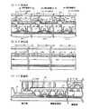
図2は、ELモジュールの上面図である。無数のTFTが設けられた基板(TFT基板とも呼ぶ)には、表示が行われる画素部40と、画素部の各画素を駆動させる駆動回路41a、41bと、EL層上に設けられる電極と引き出し配線とを接続する接続部と、外部回路と接続するためにFPCを貼り付ける端子部42とが設けられている。また、EL素子を封止するための基板と、シール材33とによって密閉する。また、図1(A)は、図2中における鎖線A−A’で切断した場合の断面図である。(Embodiment 1)
FIG. 2 is a top view of the EL module. A substrate provided with an infinite number of TFTs (also referred to as a TFT substrate) includes a pixel portion 40 on which display is performed,
鎖線A−A’の方向には規則的に画素が配置されており、ここではX方向にR、G、Bの順で配置されている例を示す。 Pixels are regularly arranged in the direction of the chain line A-A ′. Here, an example in which R, G, and B are arranged in the X direction is shown.
図1(A)中、発光領域(R)は赤色の発光領域を示しており、発光領域(G)は緑色の発光領域を示しており、発光領域(B)は青色の発光領域を示しており、これらの3色の発光領域によりフルカラー化された発光表示装置を実現している。 In FIG. 1A, the light emitting region (R) indicates a red light emitting region, the light emitting region (G) indicates a green light emitting region, and the light emitting region (B) indicates a blue light emitting region. Thus, a light emitting display device that is full-colored by these three color light emitting regions is realized.
また、図1(A)中、TFT1は、赤色を発光するEL層17に流れる電流を制御する素子であり、4、7はソース電極またはドレイン電極である。また、TFT2は、緑色を発光するEL層18に流れる電流を制御する素子であり、5、8はソース電極またはドレイン電極である。TFT3は、青色を発光するEL層19に流れる電流を制御する素子であり、6、9はソース電極またはドレイン電極である。15、16は有機絶縁材料または無機絶縁膜材料からなる層間絶縁膜である。 In FIG. 1A,
また、11〜13は、EL素子の陽極(或いは陰極)であり、20は、EL素子の陰極(或いは陽極)である。ここでは、20として薄い金属層(代表的にはMgAg、MgIn、AlLiなどの合金)と透明導電膜(ITO(酸化インジウム酸化スズ合金)、酸化インジウム酸化亜鉛合金(In2O3―ZnO)、酸化亜鉛(ZnO)等)との積層膜からなる陰極とし、各発光素子からの光を通過させている。ただし、上記透明導電膜は陰極としては機能せず、電気抵抗を下げる為に設けている。また、陽極としては、仕事関数の大きい、具体的には白金(Pt)、クロム(Cr)、タングステン(W)、もしくはニッケル(Ni)といった材料、または透明導電膜(ITO、ZnOなど)、またはこれらの積層を用いればよい。Reference numerals 11 to 13 denote anodes (or cathodes) of the EL elements, and
また、11〜13の両端部およびそれらの間は有機絶縁物24(障壁またはバンクとも呼ばれる)で覆われている。さらに、有機絶縁物24は無機絶縁膜14で覆われている。また、有機絶縁物24上の一部にまで有機化合物層が形成されている。 Further, both ends of 11 to 13 and the space between them are covered with an organic insulator 24 (also called a barrier or a bank). Further, the
また、無機絶縁膜14で覆われた有機絶縁物24(障壁またはバンクとも呼ばれる)上には、補助電極21を有している。この補助電極21は、陰極(或いは陽極)の電気抵抗値を下げる機能を有する。上記に示した透明導電膜の抵抗値は、比較的に高いため、大画面化することが困難であるが、補助電極21を設けることによって、陰極(或いは陽極)の電極全体として低抵抗化することができる。加えて、透明導電膜の薄膜化も可能とすることができる。 An
さらに、この補助電極21で下層の配線または電極と接続させる。この補助電極21はEL層を形成する前に成膜及びパターニングを行えばよい。補助電極21は、スパッタ法や蒸着法などを用い、導電型を付与する不純物元素がドープされたpoly−Si、W、WSiX、Al、Ti、Mo、Cu、Ta、Cr、またはMoから選ばれた元素、または前記元素を主成分とする合金材料もしくは化合物材料を主成分とする膜またはそれらの積層膜で形成すればよい。こうして、下層の電極とコンタクトさせた補助電極21上に接して透明導電膜を形成すれば陰極の引き出しが可能となる。なお、図1(C)は、図2中に示した鎖線C−C’で切断した場合の断面図である。また、図1(C)中、点線で示した電極同士は電気的に接続していることを示している。また、端子部において、端子の電極を陰極10と同じ材料で形成している。Further, the
また、約10μmの間隔が保たれるようにシール材33によって封止基板30が貼りつけられており、全ての発光素子は密閉されている。なお、シール材33は、駆動回路の一部と重なるようにして狭額縁化させることが好ましい。シール材33によって封止基板30を貼りつける直前には真空でアニールを行って脱気を行うことが好ましい。また、封止基板30を貼りつける際には、水素および不活性気体(希ガスまたは窒素)を含む雰囲気下で行って、保護膜32と、シール材33と、封止基板30によって密閉された空間には水素を含ませることが好ましい。発光素子を発光させた際に生じる発熱を利用することによって、上記水素を含む空間から水素を拡散させて、有機化合物層における欠陥を水素で終端させることができる。有機化合物層における欠陥を水素で終端させると発光装置としての信頼性が向上する。 Further, the sealing
さらに、色純度を高めるため、封止基板30には各画素に対応するカラーフィルタが設けられている。カラーフィルタのうち、赤色の着色層31bは赤色の発光領域(R)に対向して設けられ、緑色の着色層31cは緑色の発光領域(G)に対向して設けられ、青色の着色層31dは青色の発光領域(B)に対向して設けられる。また、発光領域以外の領域は、カラーフィルタの黒色部分、即ち遮光部31aによって遮光されている。なお、遮光部31aは、金属膜(クロム等)または黒色顔料を含有した有機膜で構成されている。 Furthermore, in order to improve color purity, the sealing
本発明においては、カラーフィルタを設けることによって円偏光板を不必要としている。 In the present invention, a circularly polarizing plate is unnecessary by providing a color filter.
また、図1(B)は、図2中に示した鎖線B−B’で切断した場合の断面図である。図1(B)においても11a〜11cの両端部およびそれらの間は無機絶縁膜14で覆われている。ここでは赤色を発光するEL層17が共通となっている例を示したが、特に限定されず、同じ色を発光する画素毎にEL層を形成してもよい。 FIG. 1B is a cross-sectional view taken along the chain line B-B ′ shown in FIG. 2. Also in FIG. 1B, both ends of 11a to 11c and the space between them are covered with an inorganic insulating
また、図1において、発光装置の信頼性を高めるために保護膜32を形成している。この保護膜32はスパッタ法により得られる窒化珪素または窒化酸化珪素を主成分とする絶縁膜である。また、図1においては、保護膜に発光を通過させるため、保護膜の膜厚は、可能な限り薄くすることが好ましい。 In FIG. 1, a
さらに、発光装置の信頼性を高めるために保護膜32を形成する前に水素を含む膜を形成する。保護膜32を形成する前に水素を含む膜を形成することによって、有機化合物層17〜19の欠陥を終端させる。前記水素を含む膜は、炭素を主成分とする薄膜、または窒化珪素膜とすればよい。この水素を含む膜を形成する方法としては、前記有機化合物層の耐えうる温度範囲、例えば室温〜100℃以下でプラズマCVD法、またはスパッタ法により形成する。なお、図1では、水素を含む膜は、保護膜の一部と見なしているため、図示していない。また、上記水素を含む膜は、保護膜32の膜応力を緩和させるバッファ層とすることもできる。 Further, in order to improve the reliability of the light emitting device, a film containing hydrogen is formed before the
また、本発明は、図1(C)に示した構成に限定されないことは言うまでもない。図1(C)と構成が一部異なる例を図3(A)〜(D)に示す。なお、簡略化のため、図3(A)〜(D)において、図1と同一である部分は、同一の符号を用いる。 Needless to say, the present invention is not limited to the structure shown in FIG. FIGS. 3A to 3D show examples in which the configuration is partly different from that in FIG. For simplification, in FIGS. 3A to 3D, the same reference numerals are used for the same portions as those in FIG.
図1(C)では、端子部に陰極と同一材料(透明電極)からなる電極が設けられた例であったが、図3(A)は、TFTのゲート電極と同一材料からなる電極(上層がW膜、下層がTaN膜)でFPCと接続する例である。 FIG. 1C shows an example in which an electrode made of the same material (transparent electrode) as the cathode is provided in the terminal portion, but FIG. 3A shows an electrode (upper layer) made of the same material as the gate electrode of the TFT. Is a W film, and a lower layer is a TaN film).
また、図3(B)は、画素電極(陽極)と同一材料からなる電極10でFPCと接続する例である。なお、この電極10は、TFTのゲート電極と同一材料からなる電極(上層がW膜、下層がTaN膜)上に接して設けられている。 FIG. 3B shows an example in which the
また、図3(C)は、TFTの引き出し配線(TiN膜、Al膜、TiN膜の順で積層された配線)上に設けられた画素電極(陽極)と同一材料からなる電極10上に形成された陰極20と同一材料(透明電極)からなる電極でFPCと接続する例である。 3C is formed on the
また、図3(D)は、TFTの引き出し配線(TiN膜、Al膜、TiN膜の順で積層された配線)上に形成された陰極20と同一材料(透明電極)からなる電極でFPCと接続する例である。 FIG. 3D shows an electrode made of the same material (transparent electrode) as the
(実施の形態2)
ここでは、水素を含む膜および保護膜について、図4を用いて説明する。(Embodiment 2)
Here, a film containing hydrogen and a protective film are described with reference to FIGS.
図4(A)は、EL素子の積層構造の一例を示した模式図である。図4(A)中、200は陰極(或いは陽極)、201はEL層、202は陽極(或いは陰極)、203は水素を含むDLC膜、204は保護膜である。また、陽極202に発光を通過させる場合、陽極202として、透光性を有する導電膜(ITOやZnOなど)を用いることが好ましい。また、陰極200としては金属膜(MgAg、MgIn、AlLiなどの合金、または周期表の1族もしくは2族に属する元素とアルミニウムとを共蒸着法により形成した膜)、あるいはそれらの積層を用いることが好ましい。 FIG. 4A is a schematic diagram illustrating an example of a stacked structure of EL elements. In FIG. 4A, 200 is a cathode (or anode), 201 is an EL layer, 202 is an anode (or cathode), 203 is a DLC film containing hydrogen, and 204 is a protective film. In the case where light emission is allowed to pass through the anode 202, a light-transmitting conductive film (such as ITO or ZnO) is preferably used as the anode 202. Further, as the cathode 200, a metal film (an alloy such as MgAg, MgIn, or AlLi, or a film formed by co-evaporation of an element belonging to
保護膜204は、スパッタ法(DC方式やRF方式)により得られる窒化珪素または窒化酸化珪素を主成分とする絶縁膜を用いればよい。シリコンターゲットを用い、窒素とアルゴンを含む雰囲気で形成すれば、窒化珪素膜が得られる。また、窒化シリコンターゲットを用いてもよい。また、保護膜204は、リモートプラズマを用いた成膜装置を用いて形成してもよい。また、保護膜に発光を通過させる場合、保護膜の膜厚は、可能な限り薄くすることが好ましい。 As the protective film 204, an insulating film mainly containing silicon nitride or silicon nitride oxide obtained by a sputtering method (a DC method or an RF method) may be used. If a silicon target is used and formed in an atmosphere containing nitrogen and argon, a silicon nitride film can be obtained. A silicon nitride target may be used. Further, the protective film 204 may be formed using a film formation apparatus using remote plasma. Moreover, when light emission is allowed to pass through the protective film, the protective film is preferably as thin as possible.
また、水素を含むDLC膜203は、炭素が70〜95原子%、水素が5〜30原子%であり、非常に硬く絶縁性に優れている。水素を含むDLC膜はプラズマCVD法(代表的には、RFプラズマCVD法、マイクロ波CVD法、電子サイクロトロン共鳴(ECR)CVD法など)、スパッタ法などで形成することができる。 In addition, the DLC film 203 containing hydrogen has 70 to 95 atomic% of carbon and 5 to 30 atomic% of hydrogen, and is extremely hard and excellent in insulating properties. The DLC film containing hydrogen can be formed by a plasma CVD method (typically, an RF plasma CVD method, a microwave CVD method, an electron cyclotron resonance (ECR) CVD method, or the like), a sputtering method, or the like.
この水素を含むDLC膜203を形成する方法としては、前記有機化合物層の耐えうる温度範囲、例えば室温〜100℃以下で形成する。 As a method of forming the DLC film 203 containing hydrogen, the DLC film 203 is formed in a temperature range that the organic compound layer can withstand, for example, room temperature to 100 ° C. or less.
プラズマを発生させる場合の成膜に用いる反応ガスは、水素ガスと、炭化水素系のガス(例えばCH4、C2H2、C6H6など)とを用いればよい。As a reaction gas used for film formation in the case of generating plasma, a hydrogen gas and a hydrocarbon-based gas (for example, CH4 , C2 H2 , C6 H6, etc.) may be used.
有機化合物層が耐えうる温度範囲で加熱処理を行ったり、発光素子を発光させた際に生じる発熱を利用することによって、上記水素を含むDLC膜から水素を拡散させて、有機化合物層における欠陥を水素で終端(ターミネーション)させることができる。有機化合物層における欠陥を水素で終端させると発光装置としての信頼性が向上する。また、上記水素を含むDLC膜の成膜の際、プラズマ化された水素によって有機化合物層における欠陥を水素で終端させることもできる。また、水素を含むDLC膜を覆って形成する保護膜は、保護膜側に拡散する水素をブロックして効率よく、水素を有機化合物層に拡散させて、有機化合物層における欠陥を水素で終端させる役目も果たす。なお、上記水素を含むDLC膜は、発光素子の保護膜としても機能させることができる。 By performing heat treatment in a temperature range that the organic compound layer can withstand or utilizing heat generated when the light emitting element emits light, hydrogen is diffused from the DLC film containing hydrogen, and defects in the organic compound layer are removed. It can be terminated with hydrogen. When defects in the organic compound layer are terminated with hydrogen, reliability as a light-emitting device is improved. Further, when the DLC film containing hydrogen is formed, defects in the organic compound layer can be terminated with hydrogen by plasma-ized hydrogen. In addition, the protective film formed to cover the DLC film containing hydrogen effectively blocks hydrogen diffused to the protective film side, efficiently diffuses hydrogen into the organic compound layer, and terminates defects in the organic compound layer with hydrogen. Also plays a role. Note that the DLC film containing hydrogen can also function as a protective film of a light-emitting element.
さらに、上記水素を含むDLC膜をバッファ層として機能させることもでき、スパッタ法により透明導電膜からなる膜に接して窒化珪素膜を形成する場合、透明導電膜に含まれる不純物(In、Sn、Zn等)が窒化珪素膜に混入する恐れがあるが、バッファ層となる上記水素を含むDLC膜を間に形成することによって窒化珪素膜への不純物混入を防止することもできる。上記構成によりバッファ層を形成することで、透明導電膜からの不純物(In、Snなど)の混入を防止し、不純物のない優れた保護膜を形成することができる。 Furthermore, the DLC film containing hydrogen can also function as a buffer layer. When a silicon nitride film is formed in contact with a film made of a transparent conductive film by a sputtering method, impurities (In, Sn, Zn, etc.) may be mixed into the silicon nitride film. However, impurities can be prevented from being mixed into the silicon nitride film by forming the DLC film containing hydrogen as a buffer layer therebetween. By forming the buffer layer with the above structure, impurities (In, Sn, etc.) from the transparent conductive film can be prevented from mixing, and an excellent protective film free of impurities can be formed.
このような構成とすることで、発光素子を保護するとともに、信頼性を向上させることができる。With such a structure, the light emitting element can be protected and the reliability can be improved.
また、図4(B)は、EL素子の積層構造の他の一例を示した模式図である。図4(B)中、300は陰極(或いは陽極)、301はEL層、302は陽極(或いは陰極)、303は水素を含む窒化珪素膜、304は保護膜である。また、陽極302に発光を通過させる場合、302として、透光性を有する導電性材料または非常に薄い金属膜(MgAg)、あるいはそれらの積層を用いることが好ましい。また、陽極302に発光を通過させる場合、陽極302として、透光性を有する導電膜(ITOやZnOなど)を用いることが好ましい。また、陰極300としては金属膜(MgAg、MgIn、AlLiなどの合金、または周期表の1族もしくは2族に属する元素とアルミニウムとを共蒸着法により形成した膜)、あるいはそれらの積層を用いることが好ましい。 FIG. 4B is a schematic view illustrating another example of a stacked structure of EL elements. In FIG. 4B, 300 is a cathode (or anode), 301 is an EL layer, 302 is an anode (or cathode), 303 is a silicon nitride film containing hydrogen, and 304 is a protective film. In the case where light emission is allowed to pass through the anode 302, it is preferable to use a light-transmitting conductive material, a very thin metal film (MgAg), or a laminate thereof as 302. In the case where light emission is allowed to pass through the anode 302, a light-transmitting conductive film (such as ITO or ZnO) is preferably used as the anode 302. Further, as the cathode 300, a metal film (an alloy such as MgAg, MgIn, or AlLi, or a film formed by co-evaporation of an element belonging to
保護膜304は、スパッタ法(DC方式やRF方式)により得られる窒化珪素または窒化酸化珪素を主成分とする絶縁膜を用いればよい。シリコンターゲットを用い、窒素とアルゴンを含む雰囲気で形成すれば、窒化珪素膜が得られる。また、窒化シリコンターゲットを用いてもよい。また、保護膜304は、リモートプラズマを用いた成膜装置を用いて形成してもよい。また、保護膜に発光を通過させる場合、保護膜の膜厚は、可能な限り薄くすることが好ましい。 As the protective film 304, an insulating film mainly containing silicon nitride or silicon nitride oxide obtained by a sputtering method (DC method or RF method) may be used. If a silicon target is used and formed in an atmosphere containing nitrogen and argon, a silicon nitride film can be obtained. A silicon nitride target may be used. Further, the protective film 304 may be formed using a film formation apparatus using remote plasma. Moreover, when light emission is allowed to pass through the protective film, the protective film is preferably as thin as possible.
また、水素を含む窒化珪素膜303は、プラズマCVD法(代表的には、RFプラズマCVD法、マイクロ波CVD法、電子サイクロトロン共鳴(ECR)CVD法など)、RFスパッタ法、DCスパッタ法などで形成することができる。 The silicon nitride film 303 containing hydrogen is formed by a plasma CVD method (typically, an RF plasma CVD method, a microwave CVD method, an electron cyclotron resonance (ECR) CVD method, etc.), an RF sputtering method, a DC sputtering method, or the like. Can be formed.
この水素を含む窒化珪素膜303を形成する方法としては、前記有機化合物層の耐えうる温度範囲、例えば室温〜100℃以下で形成する。 As a method for forming the silicon nitride film 303 containing hydrogen, the silicon compound film 303 is formed in a temperature range that the organic compound layer can withstand, for example, room temperature to 100 ° C. or less.
水素を含む窒化珪素膜303を形成する方法として、プラズマCVD法を用いる場合、反応ガスは、窒素を含むガス(N2、NH3NOxで表記される窒素酸化物系ガスなど)と、珪化水素系のガス(例えばシラン(SiH4)やジシランやトリシランなど)とを用いればよい。In the case where a plasma CVD method is used as a method for forming the silicon nitride film 303 containing hydrogen, a reactive gas is a gas containing nitrogen (such as a nitrogen oxide-based gas represented by N2 or NH3 NOx), hydrogen silicide, or the like. A system gas (for example, silane (SiH4 ), disilane, trisilane, or the like) may be used.
水素を含む窒化珪素膜303を形成する方法として、スパッタ法を用いる場合、シリコンターゲットを用い、水素と窒素とアルゴンとを含む雰囲気で形成すれば、水素を含む窒化珪素膜が得られる。また、窒化シリコンターゲットを用いてもよい。 When a sputtering method is used as a method for forming the silicon nitride film 303 containing hydrogen, a silicon nitride film containing hydrogen can be obtained by using a silicon target and forming it in an atmosphere containing hydrogen, nitrogen, and argon. A silicon nitride target may be used.
有機化合物層が耐えうる温度範囲で加熱処理を行ったり、発光素子を発光させた際に生じる発熱を利用することによって、上記水素を含む窒化珪素膜から水素を拡散させて、有機化合物層における欠陥を水素で終端(ターミネーション)させることができる。有機化合物層における欠陥を水素で終端させると発光装置としての信頼性が向上する。また、上記水素を含む窒化珪素膜の成膜の際、プラズマ化された水素によって有機化合物層における欠陥を水素で終端させることもできる。また、水素を含む窒化珪素膜を覆って形成する保護膜は、保護膜側に拡散する水素をブロックして効率よく、水素を有機化合物層に拡散させて、有機化合物層における欠陥を水素で終端させる役目も果たす。なお、上記水素を含む窒化珪素膜は、発光素子の保護膜としても機能させることができる。 By performing heat treatment in a temperature range that the organic compound layer can withstand or utilizing heat generated when the light emitting element emits light, hydrogen is diffused from the silicon nitride film containing hydrogen to cause defects in the organic compound layer. Can be terminated with hydrogen. When defects in the organic compound layer are terminated with hydrogen, reliability as a light-emitting device is improved. Further, when the silicon nitride film containing hydrogen is formed, defects in the organic compound layer can be terminated with hydrogen by plasma-ized hydrogen. In addition, the protective film formed over the silicon nitride film containing hydrogen effectively blocks hydrogen diffused to the protective film side, effectively diffuses hydrogen into the organic compound layer, and terminates defects in the organic compound layer with hydrogen. Also plays the role of letting. Note that the silicon nitride film containing hydrogen can also function as a protective film of the light-emitting element.
さらに、上記水素を含む窒化珪素膜をバッファ層として機能させることもでき、スパッタ法により透明導電膜からなる膜に接して窒化珪素膜を形成する場合、透明導電膜に含まれる不純物(In、Sn、Zn等)が窒化珪素膜に混入する恐れがあるが、バッファ層となる上記水素を含む窒化珪素膜を間に形成することによって窒化珪素膜への不純物混入を防止することもできる。上記構成によりバッファ層を形成することで、透明導電膜からの不純物(In、Snなど)の混入を防止し、不純物のない優れた保護膜を形成することができる。 Further, the silicon nitride film containing hydrogen can also function as a buffer layer. When a silicon nitride film is formed in contact with a film made of a transparent conductive film by a sputtering method, impurities (In, Sn) contained in the transparent conductive film are formed. , Zn, or the like) may be mixed into the silicon nitride film, but the silicon nitride film containing hydrogen serving as a buffer layer may be formed therebetween to prevent impurities from entering the silicon nitride film. By forming the buffer layer with the above structure, impurities (In, Sn, etc.) from the transparent conductive film can be prevented from mixing, and an excellent protective film free of impurities can be formed.
このような構成とすることで、発光素子を保護するとともに、信頼性を向上させることができる。With such a structure, the light emitting element can be protected and the reliability can be improved.
また、図4(A)及び図4(B)では水素を含む膜として単層とした例を示したが、水素を含む窒化珪素膜と水素を含むDLC膜との積層、もしくはこれらの3層以上の積層としてもよい。 4A and 4B show an example in which a single layer is formed as a film containing hydrogen. However, a stack of a silicon nitride film containing hydrogen and a DLC film containing hydrogen, or these three layers are used. It is good also as the above lamination | stacking.
また、本実施の形態は、アクティブマトリクス型表示装置だけでなく、パッシブ型表示装置に適用することもできる。Further, this embodiment can be applied not only to an active matrix display device but also to a passive display device.
また、本実施の形態は、実施の形態1と自由に組み合わせることができる。 Further, this embodiment mode can be freely combined with
(実施の形態3)
ここでは、図1と構成が一部異なる例を図6に示す。ここでは、画素部に規則的に配置される多数の画素のうち、3×3の画素を例に本発明を以下に説明する。なお、断面構造において、TFTは図1とほぼ同一であり、簡略化のため、図6において、図1と同一である部分は、同一の符号を用いる。(Embodiment 3)
Here, an example in which the configuration is partially different from that in FIG. 1 is shown in FIG. Here, the present invention will be described below by taking a 3 × 3 pixel as an example among many pixels regularly arranged in the pixel portion. In the cross-sectional structure, the TFT is almost the same as that in FIG. 1. For the sake of simplification, the same reference numerals are used in FIG. 6 for the same portions as those in FIG.
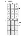
図6(A)は、図5(A)中鎖線A−A’で切断した場合の断面図である。発光領域50Rは赤色の発光領域を示しており、発光領域50Gは緑色の発光領域を示しており、発光領域50Bは青色の発光領域を示しており、これらの3色の発光領域によりフルカラー化された発光表示装置を実現している。 FIG. 6A is a cross-sectional view taken along the chain line A-A ′ in FIG. The
本実施の形態においては、図6(A)に示したように、同一のマスクでパターンニングを行った例であり、補助電極621と有機絶縁物624との上面から見た形状がほぼ同一である。この場合、図6(C)に示したように、補助電極621は、陰極20でソース配線と同一材料からなる配線と電気的に接続させている。In this embodiment mode, as shown in FIG. 6A, patterning is performed using the same mask, and the shapes of the
また、画素電極612は、層間絶縁膜15上に形成されており、画素電極612の形成後にTFTのコンタクトホールが形成され、その後に形成される電極607、608でTFTと画素電極612とを電気的に接続している。また、画素電極の両端部およびそれらの間は無機絶縁物14で覆われている。また、図1と同様に有機絶縁物624上の一部にまで有機化合物層が形成されている。 Further, the pixel electrode 612 is formed on the
また、図5(B)は、画素電極の形成直後の上面図であり、図5(A)と対応している。図5(A)及び図5(B)においては、画素一列(Y方向)毎に帯状の有機化合物層を設けている。各発色の異なる有機化合物層の間には帯状に有機絶縁物624が設けられている。また、図5(A)においては、画素一列(Y方向)毎に有機絶縁物624および補助配線621を設ける構成としている。 FIG. 5B is a top view immediately after formation of the pixel electrode, and corresponds to FIG. 5A and 5B, a strip-shaped organic compound layer is provided for each pixel row (Y direction). Between the organic compound layers having different colors, an
また、図7(A)は、図5、図6に対応する上面図である。図7(A)中、左側に示した図における接続部の一部断面図を右側に示し、図6(C)と同一箇所である。また、図7(A)に示した補助配線621及び有機絶縁物をパターニングする場合、用いるメタルマスクの例を図8(A)に示した。 FIG. 7A is a top view corresponding to FIGS. 5 and 6. In FIG. 7A, a partial cross-sectional view of the connection portion in the diagram shown on the left side is shown on the right side, which is the same as FIG. 6C. FIG. 8A shows an example of a metal mask to be used when patterning the
また、有機絶縁物と補助電極とのトータルの膜厚が比較的厚くなった場合、段差が大きくなるため、透明導電膜で電気的に接続することが困難になる可能性がある。特に、透明導電膜の薄膜化を行った場合にカバレッジ不良により線欠陥が生じる恐れがある。そこで、補助電極621と下層の電極との接続をより確実にするため、図7(B)に示すように、マスク数を増やして622で示す電極を形成してもよい。また、メタルマスクを用いて蒸着法により電極622を形成してもよい。 In addition, when the total film thickness of the organic insulator and the auxiliary electrode becomes relatively large, the step becomes large, and it may be difficult to electrically connect with the transparent conductive film. In particular, when the transparent conductive film is thinned, a line defect may occur due to poor coverage. Therefore, in order to make the connection between the
また、図7(C)に示すように、予め画素部の周りにソース配線と同一材料からなる配線623を設けておき、さらに補助電極621と直交するように第2の補助電極625を形成してもよい。こうすることによって、第2の補助電極625は、補助電極621に直接接して設けられ、且つ、配線623とも直接接することができる。なお、補助電極621と第2の補助電極625との間が発光領域となるように適宜設計する。また、図7(A)に示した第2の補助電極625をパターニングする場合、用いるメタルマスクの例を図8(B)に示した。 As shown in FIG. 7C, a
また、図7(C)では2回のパターニングによって第1の補助電極621と第2の補助電極625とを形成した例を示したが、図8(C)に示したメタルマスクを用いて格子状に補助電極を形成してもよい。図8(C)の右側図で示すように各開口部は細い線で区切られているが、蒸着では回り込みがあるため、一部膜厚が薄くなるものの格子状に補助電極を形成することができる。 FIG. 7C shows an example in which the first
また、本実施の形態は、実施の形態1または実施の形態2と自由に組み合わせることができる。 Further, this embodiment can be freely combined with
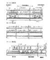
(実施の形態4)
ここでは、図1と構成が一部異なる例を図9に示す。ここでは、画素部に規則的に配置される多数の画素のうち、3×3の画素を例に本発明を以下に説明する。なお、断面構造において、有機絶縁物24が存在しない点と、全面に高分子からなる有機化合物層60が存在する点以外は図1とほぼ同一であり、簡略化のため、図9において、図1と同一である部分は、同一の符号を用いる。また、図9(A)は、図2中における鎖線A−A’で切断した場合の断面図である。(Embodiment 4)
Here, FIG. 9 shows an example in which the configuration is partially different from FIG. Here, the present invention will be described below by taking a 3 × 3 pixel as an example among many pixels regularly arranged in the pixel portion. The cross-sectional structure is substantially the same as that in FIG. 1 except that the
図1に示した有機絶縁物24が図9に示す構造には存在せず、その代わりに無機絶縁膜14と補助電極721とで各有機化合物17、18、19の間隔を保っている。 The
また、高分子からなる有機化合物層60(代表的にはポリ(エチレンジオキシチオフェン)/ポリ(スチレンスルホン酸)水溶液(以下、「PEDOT/PSS」と記す)、ちなみに、このPEDOT/PSSは、正孔注入層として作用する。)は、スピンコート法やスプレー法などの塗布法で形成するため、全面に形成される。また、高分子からなる有機化合物層60は導電性を有しており、陰極20と補助電極721は電気的に接続される。補助電極721を設けることによって、陰極(或いは陽極)全体として低抵抗化することができる。加えて、透明導電膜の薄膜化も可能とすることができる。さらに、この補助電極721で下層の配線または電極と接続させる。この補助電極721はEL層を形成する前に成膜及びパターニングを行えばよい。下層の電極とコンタクトさせた補助電極721上に透明導電膜を形成すれば陰極の引き出しが可能となる。なお、図9(C)は、図2中に示した鎖線C−C’で切断した場合の断面図である。また、図9(C)中、点線で示した電極同士は電気的に接続していることを示している。また、端子部において、端子の電極を陰極20と同じ材料で形成している。In addition, an
また、図9(B)は、図2中に示した鎖線B−B’で切断した場合の断面図である。図9(B)においても11a〜11cの両端部およびそれらの間は無機絶縁物14で覆われている。ここでは赤色を発光するEL層17が共通となっている例を示したが、特に限定されず、同じ色を発光する画素毎にEL層を形成してもよい。 FIG. 9B is a cross-sectional view taken along the chain line B-B ′ shown in FIG. 2. 9B, both ends of 11a to 11c and the space between them are covered with the
また、本実施の形態は、実施の形態1、実施の形態2、または実施の形態3と自由に組み合わせることができる。 Further, this embodiment mode can be freely combined with
(実施の形態5)
ここでは、図1と構成が一部異なる例を図10に示す。ここでは、画素部に規則的に配置される多数の画素のうち、3×3の画素を例に本発明を以下に説明する。なお、断面構造において、陰極20上に補助配線821が存在する点以外は図1とほぼ同一であり、簡略化のため、図10において、図1と同一である部分は、同一の符号を用いる。また、図10(A)は、図2中における鎖線A−A’で切断した場合の断面図である。(Embodiment 5)
Here, FIG. 10 shows an example in which the configuration is partially different from FIG. Here, the present invention will be described below by taking a 3 × 3 pixel as an example among many pixels regularly arranged in the pixel portion. Note that the cross-sectional structure is substantially the same as that in FIG. 1 except that the
また、補助電極821は、陰極上に形成するため、メタルマスクを用いた蒸着法で行う。ここでは格子状に補助電極821を形成した例を示す。補助電極821を設けることによって、陰極(或いは陽極)全体として低抵抗化することができる。加えて、透明導電膜の薄膜化も可能とすることができる。さらに、この補助電極821で下層の配線または電極と接続させる。下層の電極とコンタクトさせた補助電極821上に透明導電膜を形成すれば陰極の引き出しが可能となる。なお、図10(C)は、図2中に示した鎖線C−C’で切断した場合の断面図である。また、図10(C)中、点線で示した電極同士は電気的に接続していることを示している。また、端子部において、端子の電極を陰極20と同じ材料で形成している。 In addition, since the
また、本実施の形態は、実施の形態1、実施の形態2、実施の形態3、または実施の形態4と自由に組み合わせることができる。 In addition, this embodiment mode can be freely combined with
以上の構成でなる本発明について、以下に示す実施例でもってさらに詳細な説明を行うこととする。 The present invention having the above-described configuration will be described in more detail with the following examples.
本実施例では、絶縁表面上に作製したアクティブマトリクス型発光装置について説明する。なお、能動素子としてここでは薄膜トランジスタ(以下、「TFT」と記す)を用いているが、MOSトランジスタを用いてもよい。In this example, an active matrix light-emitting device manufactured over an insulating surface is described. Here, a thin film transistor (hereinafter referred to as “TFT”) is used as an active element, but a MOS transistor may be used.
また、TFTとしてトップゲート型TFT(具体的にはプレーナ型TFT)を例示するが、ボトムゲート型TFT(典型的には逆スタガ型TFT)を用いることもできる。 Further, although a top gate TFT (specifically, a planar TFT) is exemplified as the TFT, a bottom gate TFT (typically an inverted staggered TFT) can also be used.
本実施例では、基板としてバリウムホウケイ酸ガラス、またはアルミノホウケイ酸ガラスなどのガラスからなる基板、石英基板やシリコン基板、金属基板またはステンレス基板の表面に絶縁膜を形成したものを用いればよい。また、本実施例の処理温度に耐えうる耐熱性が有するプラスチック基板を用いてもよいし、可撓性基板を用いても良い。 In this embodiment, a substrate made of glass such as barium borosilicate glass or alumino borosilicate glass, a quartz substrate, a silicon substrate, a metal substrate, or a stainless steel substrate with an insulating film formed thereon may be used. Further, a plastic substrate having heat resistance that can withstand the processing temperature of this embodiment may be used, or a flexible substrate may be used.
まず、厚さ0.7mmの耐熱性ガラス基板上にプラズマCVD法により下地絶縁膜の下層として、プラズマCVD法で成膜温度400℃、原料ガスSiH4、NH3、N2Oから作製される酸化窒化シリコン膜(組成比Si=32%、O=27%、N=24%、H=17%)を50nm(好ましくは10〜200nm)形成する。次いで、表面をオゾン水で洗浄した後、表面の酸化膜を希フッ酸(1/100希釈)で除去する。次いで、下地絶縁膜の上層として、プラズマCVD法で成膜温度400℃、原料ガスSiH4、N2Oから作製される酸化窒化シリコン膜(組成比Si=32%、O=59%、N=7%、H=2%)を100nm(好ましくは50〜200nm)の厚さに積層形成し、さらに大気解放せずにプラズマCVD法で成膜温度300℃、成膜ガスSiH4で非晶質構造を有する半導体膜(ここではアモルファスシリコン膜)を54nmの厚さ(好ましくは25〜200nm)で形成する。First, on a heat-resistant glass substrate having a thickness of 0.7 mm, a lower layer of a base insulating film is formed by plasma CVD method from a film forming temperature of 400 ° C. and source gases SiH4 , NH3 and N2 O by plasma CVD method. A silicon oxynitride film (composition ratio Si = 32%, O = 27%, N = 24%, H = 17%) is formed to 50 nm (preferably 10 to 200 nm). Next, after cleaning the surface with ozone water, the oxide film on the surface is removed with dilute hydrofluoric acid (1/100 dilution). Next, as an upper layer of the base insulating film, a silicon oxynitride film (composition ratio Si = 32%, O = 59%, N = N) is formed from a source gas SiH4 and N2 O by a plasma CVD method at a deposition temperature of 400 ° C. 7%, H = 2%) is laminated to a thickness of 100 nm (preferably 50 to 200 nm), and further, the film is amorphous by plasma CVD with a film forming temperature of 300 ° C. and a film forming gas of SiH4 without being released to the atmosphere. A semiconductor film having a structure (here, an amorphous silicon film) is formed with a thickness of 54 nm (preferably 25 to 200 nm).
本実施例では下地絶縁膜を2層構造として示したが、珪素を主成分とする絶縁膜の単層膜または2層以上積層させた構造として形成しても良い。また、半導体膜の材料に限定はないが、好ましくはシリコンまたはシリコンゲルマニウム(SiXGe1-X(X=0.0001〜0.02))合金などを用い、公知の手段(スパッタ法、LPCVD法、またはプラズマCVD法等)により形成すればよい。また、プラズマCVD装置は、枚葉式の装置でもよいし、バッチ式の装置でもよい。また、同一の成膜室で大気に触れることなく下地絶縁膜と半導体膜とを連続成膜してもよい。Although the base insulating film is shown as a two-layer structure in this embodiment, it may be formed as a single layer film of an insulating film containing silicon as a main component or a structure in which two or more layers are stacked. The material of the semiconductor film is not limited, but preferably, silicon or silicon germanium (Six Ge1-x (X = 0.0001 to 0.02)) alloy or the like is used, and known means (sputtering method, LPCVD) Or a plasma CVD method or the like). The plasma CVD apparatus may be a single wafer type apparatus or a batch type apparatus. Alternatively, the base insulating film and the semiconductor film may be successively formed without being exposed to the air in the same film formation chamber.
次いで、非晶質構造を有する半導体膜の表面を洗浄した後、オゾン水で表面に約2nmの極薄い酸化膜を形成する。次いで、TFTのしきい値を制御するために微量な不純物元素(ボロンまたはリン)のドーピングを行う。ここでは、ジボラン(B2H6)を質量分離しないでプラズマ励起したイオンドープ法を用い、ドーピング条件を加速電圧15kV、ジボランを水素で1%に希釈したガスを流量30sccmとし、ドーズ量2×10¹²/cm2で非晶質シリコン膜にボロンを添加する。Next, after cleaning the surface of the semiconductor film having an amorphous structure, an extremely thin oxide film of about 2 nm is formed on the surface with ozone water. Next, a small amount of impurity element (boron or phosphorus) is doped in order to control the threshold value of the TFT. Here, an ion doping method in which diborane (B2 H6 ) is plasma-excited without mass separation is used, the doping conditions are an acceleration voltage of 15 kV, a gas obtained by diluting diborane to 1% with hydrogen at a flow rate of 30 sccm, and a dose amount of 2 × Boron is added to the amorphous silicon film at 1012 / cm2 .
次いで、重量換算で10ppmのニッケルを含む酢酸ニッケル塩溶液をスピナーで塗布した。塗布に代えてスパッタ法でニッケル元素を全面に散布する方法を用いてもよい。 Next, a nickel acetate salt solution containing 10 ppm of nickel in terms of weight was applied with a spinner. Instead of coating, a method of spreading nickel element over the entire surface by sputtering may be used.
次いで、加熱処理を行い結晶化させて結晶構造を有する半導体膜を形成する。この加熱処理は、電気炉の熱処理または強光の照射を用いればよい。電気炉の熱処理で行う場合は、500℃〜650℃で4〜24時間で行えばよい。ここでは脱水素化のための熱処理(500℃、1時間)の後、結晶化のための熱処理(550℃、4時間)を行って結晶構造を有するシリコン膜を得た。なお、ここでは炉を用いた熱処理を用いて結晶化を行ったが、短時間での結晶化が可能なランプアニール装置で結晶化を行ってもよい。 Next, heat treatment is performed for crystallization, so that a semiconductor film having a crystal structure is formed. For this heat treatment, heat treatment in an electric furnace or irradiation with strong light may be used. When the heat treatment is performed in an electric furnace, the heat treatment may be performed at 500 ° C. to 650 ° C. for 4 to 24 hours. Here, after heat treatment for dehydrogenation (500 ° C., 1 hour), heat treatment for crystallization (550 ° C., 4 hours) was performed to obtain a silicon film having a crystal structure. Although crystallization is performed here using heat treatment using a furnace, crystallization may be performed using a lamp annealing apparatus capable of crystallization in a short time.
次いで、結晶構造を有するシリコン膜表面の酸化膜を希フッ酸等で除去した後、大粒径な結晶を得るため、連続発振が可能な固体レーザを用い、基本波の第2高調波〜第4高調波を半導体膜に照射する。レーザ光の照射は大気中、または酸素雰囲気中で行う。なお、大気中、または酸素雰囲気中で行うため、レーザー光の照射により表面に酸化膜が形成される。代表的には、Nd:YVO4レーザー(基本波1064nm)の第2高調波(532nm)や第3高調波(355nm)を適用すればよい。出力10Wの連続発振のYVO4レーザから射出されたレーザ光を非線形光学素子により高調波に変換する。また、共振器の中にYVO4結晶と非線形光学素子を入れて、高調波を射出する方法もある。そして、好ましくは光学系により照射面にて矩形状または楕円形状のレーザ光に成形して、被処理体に照射する。このときのエネルギー密度は0.01〜100MW/cm2程度(好ましくは0.1〜10MW/cm2)が必要である。そして、10〜2000cm/s程度の速度でレーザ光に対して相対的に半導体膜を移動させて照射すればよい。Next, after removing the oxide film on the surface of the silicon film having a crystal structure with dilute hydrofluoric acid or the like, a solid-state laser capable of continuous oscillation is used to obtain a crystal having a large grain size, and the second harmonic to the second fundamental wave Irradiate the semiconductor film with the fourth harmonic. Laser irradiation is performed in the air or in an oxygen atmosphere. Note that since the reaction is performed in the air or in an oxygen atmosphere, an oxide film is formed on the surface by laser light irradiation. Typically, a second harmonic (532 nm) or a third harmonic (355 nm) of an Nd: YVO4 laser (fundamental wave 1064 nm) may be applied. Laser light emitted from a continuous wave YVO4 laser having an output of 10 W is converted into a harmonic by a non-linear optical element. There is also a method of emitting harmonics by putting a YVO4 crystal and a nonlinear optical element in a resonator. Then, it is preferably formed into a rectangular or elliptical laser beam on the irradiation surface by an optical system, and irradiated to the object to be processed. At this time, the energy density of approximately 0.01 to 100 MW / cm2 (preferably 0.1 to 10 MW / cm2) is required. Then, irradiation may be performed by moving the semiconductor film relative to the laser light at a speed of about 10 to 2000 cm / s.
もちろん、連続発振のYVO4レーザーの第2高調波を照射する前の結晶構造を有するシリコン膜を用いてTFTを作製することもできるが、レーザ光照射後の結晶構造を有するシリコン膜のほうが結晶性が向上しているため、TFTの電気的特性が向上するので望ましい。例えば、上記レーザ光照射前の結晶構造を有するシリコン膜を用いてTFTを作製すると、移動度は300cm2/Vs程度であるが、上記レーザ光照射後の結晶構造を有するシリコン膜を用いてTFTを作製すると、移動度は500〜600cm2/Vs程度と著しく向上する。Of course, a TFT can also be manufactured using a silicon film having a crystal structure before irradiation with the second harmonic of a continuous wave YVO4 laser, but a silicon film having a crystal structure after laser light irradiation is more crystalline. Therefore, it is desirable because the electrical characteristics of the TFT are improved. For example, when a TFT is manufactured using a silicon film having a crystal structure before laser light irradiation, the mobility is about 300 cm2 / Vs, but the TFT is formed using a silicon film having a crystal structure after laser light irradiation. The mobility is remarkably improved to about 500 to 600 cm2 / Vs.
なお、ここではシリコンの結晶化を助長する金属元素としてニッケルを用いて結晶化させた後、さらに連続発振のYVO4レーザーの第2高調波を照射したが、特に限定されず、非晶質構造を有するシリコン膜を成膜し、脱水素化のための熱処理を行った後、上記連続発振のYVO4レーザーの第2高調波を照射して結晶構造を有するシリコン膜を得てもよい。Here, after crystallization using nickel as a metal element for promoting crystallization of silicon, the second harmonic of a continuous wave YVO4 laser was further irradiated. A silicon film having a crystalline structure may be obtained by irradiating the second harmonic of the above continuous wave YVO4 laser after forming a silicon film having a thermal conductivity for dehydrogenation.
また、連続発振のレーザに代えてパルス発振のレーザを用いることもでき、パルス発振のエキシマレーザを用いる場合には、周波数300Hzとし、レーザーエネルギー密度を100〜1000mJ/cm2(代表的には200〜800mJ/cm2)とするのが望ましい。このとき、レーザ光を50〜98%オーバーラップさせても良い。Further, a pulsed laser can be used instead of a continuous wave laser. When a pulsed excimer laser is used, the frequency is set to 300 Hz and the laser energy density is set to 100 to 1000 mJ / cm2 (typically 200 ˜800 mJ / cm2 ) is desirable. At this time, the laser beams may be overlapped by 50 to 98%.
次いで、上記レーザー光の照射により形成された酸化膜に加え、オゾン水で表面を120秒処理して合計1〜5nmの酸化膜からなるバリア層を形成する。本実施例ではオゾン水を用いてバリア層を形成したが、酸素雰囲気下の紫外線の照射で結晶構造を有する半導体膜の表面を酸化する方法や酸素プラズマ処理により結晶構造を有する半導体膜の表面を酸化する方法やプラズマCVD法やスパッタ法や蒸着法などで1〜10nm程度の酸化膜を堆積してバリア層を形成してもよい。また、バリア層を形成する前にレーザー光の照射により形成された酸化膜を除去してもよい。Next, in addition to the oxide film formed by the laser light irradiation, the surface is treated with ozone water for 120 seconds to form a barrier layer made of an oxide film having a total thickness of 1 to 5 nm. In this embodiment, ozone water is used to form the barrier layer. However, the surface of the semiconductor film having a crystal structure is oxidized by a method of oxidizing the surface of the semiconductor film having a crystal structure by irradiation with ultraviolet rays in an oxygen atmosphere or the surface of the semiconductor film having a crystal structure by oxygen plasma treatment. The barrier layer may be formed by depositing an oxide film of about 1 to 10 nm by an oxidation method, a plasma CVD method, a sputtering method, an evaporation method, or the like. Further, the oxide film formed by laser light irradiation may be removed before forming the barrier layer.
次いで、上記バリア層上にプラズマCVD法またはスパッタ法でゲッタリングサイトとなるアルゴン元素を含む非晶質シリコン膜を50nm〜400nm、ここでは膜厚150nmで形成する。本実施例では、スパッタ法でシリコンターゲットを用い、アルゴン雰囲気下、圧力0.3Paで成膜する。 Next, an amorphous silicon film containing an argon element serving as a gettering site is formed with a thickness of 50 nm to 400 nm, here 150 nm, over the barrier layer by plasma CVD or sputtering. In this embodiment, a silicon target is used by a sputtering method, and a film is formed at a pressure of 0.3 Pa in an argon atmosphere.
その後、650℃に加熱された炉に入れて3分の熱処理を行いゲッタリングして、結晶構造を有する半導体膜中のニッケル濃度を低減する。炉に代えてランプアニール装置を用いてもよい。After that, heat treatment is performed for 3 minutes in a furnace heated to 650 ° C., and gettering is performed to reduce the nickel concentration in the semiconductor film having a crystal structure. A lamp annealing apparatus may be used instead of the furnace.
次いで、バリア層をエッチングストッパーとして、ゲッタリングサイトであるアルゴン元素を含む非晶質シリコン膜を選択的に除去した後、バリア層を希フッ酸で選択的に除去する。なお、ゲッタリングの際、ニッケルは酸素濃度の高い領域に移動しやすい傾向があるため、酸化膜からなるバリア層をゲッタリング後に除去することが望ましい。 Next, the amorphous silicon film containing an argon element as a gettering site is selectively removed using the barrier layer as an etching stopper, and then the barrier layer is selectively removed with dilute hydrofluoric acid. Note that during gettering, nickel tends to move to a region with a high oxygen concentration, and thus it is desirable to remove the barrier layer made of an oxide film after gettering.
次いで、得られた結晶構造を有するシリコン膜(ポリシリコン膜とも呼ばれる)の表面にオゾン水で薄い酸化膜を形成した後、レジストからなるマスクを形成し、所望の形状にエッチング処理して島状に分離された半導体層を形成する。半導体層を形成した後、レジストからなるマスクを除去する。 Next, after forming a thin oxide film with ozone water on the surface of the obtained silicon film having a crystal structure (also called a polysilicon film), a mask made of resist is formed and etched into a desired shape to form an island shape. A separated semiconductor layer is formed. After the semiconductor layer is formed, the resist mask is removed.
次いで、フッ酸を含むエッチャントで酸化膜を除去すると同時にシリコン膜の表面を洗浄した後、ゲート絶縁膜となる珪素を主成分とする絶縁膜を形成する。ここでは、プラズマCVD法により115nmの厚さで酸化窒化シリコン膜(組成比Si=32%、O=59%、N=7%、H=2%)で形成した。 Next, the oxide film is removed with an etchant containing hydrofluoric acid, and at the same time, the surface of the silicon film is washed, and then an insulating film containing silicon as a main component and serving as a gate insulating film is formed. Here, a silicon oxynitride film (composition ratio: Si = 32%, O = 59%, N = 7%, H = 2%) with a thickness of 115 nm is formed by plasma CVD.
次いで、ゲート絶縁膜上に膜厚20〜100nmの第1の導電膜と、膜厚100〜400nmの第2の導電膜とを積層形成する。本実施例では、ゲート絶縁膜上に膜厚50nmの窒化タンタル膜、膜厚370nmのタングステン膜を順次積層し、以下に示す手順でパターニングを行って各ゲート電極及び各配線を形成する。 Next, a first conductive film with a thickness of 20 to 100 nm and a second conductive film with a thickness of 100 to 400 nm are stacked over the gate insulating film. In this embodiment, a tantalum nitride film having a thickness of 50 nm and a tungsten film having a thickness of 370 nm are sequentially stacked on the gate insulating film, and patterning is performed in the following procedure to form each gate electrode and each wiring.
第1の導電膜及び第2の導電膜を形成する導電性材料としてはTa、W、Ti、Mo、Al、Cuから選ばれた元素、または前記元素を主成分とする合金材料もしくは化合物材料で形成する。また、第1の導電膜及び第2の導電膜としてリン等の不純物元素をドーピングした多結晶シリコン膜に代表される半導体膜や、、AgPdCu合金を用いてもよい。また、2層構造に限定されず、例えば、膜厚50nmのタングステン膜、膜厚500nmのアルミニウムとシリコンの合金(Al−Si)膜、膜厚30nmの窒化チタン膜を順次積層した3層構造としてもよい。また、3層構造とする場合、第1の導電膜のタングステンに代えて窒化タングステンを用いてもよいし、第2の導電膜のアルミニウムとシリコンの合金(Al−Si)膜に代えてアルミニウムとチタンの合金膜(Al−Ti)を用いてもよいし、第3の導電膜の窒化チタン膜に代えてチタン膜を用いてもよい。また、単層構造であってもよい。 The conductive material for forming the first conductive film and the second conductive film is an element selected from Ta, W, Ti, Mo, Al, and Cu, or an alloy material or a compound material containing the element as a main component. Form. Alternatively, a semiconductor film typified by a polycrystalline silicon film doped with an impurity element such as phosphorus, or an AgPdCu alloy may be used as the first conductive film and the second conductive film. Further, the present invention is not limited to the two-layer structure. For example, a three-layer structure in which a 50 nm-thickness tungsten film, a 500 nm-thick aluminum and silicon alloy (Al-Si) film, and a 30 nm-thickness titanium nitride film are sequentially stacked. Also good. In the case of a three-layer structure, tungsten nitride may be used instead of tungsten of the first conductive film, or aluminum instead of the aluminum and silicon alloy (Al-Si) film of the second conductive film. A titanium alloy film (Al—Ti) may be used, or a titanium film may be used instead of the titanium nitride film of the third conductive film. Moreover, a single layer structure may be sufficient.
上記第1の導電膜及び第2の導電膜のエッチング(第1のエッチング処理および第2のエッチング処理)にはICP(Inductively Coupled Plasma:誘導結合型プラズマ)エッチング法を用いると良い。ICPエッチング法を用い、エッチング条件(コイル型の電極に印加される電力量、基板側の電極に印加される電力量、基板側の電極温度等)を適宜調節することによって所望のテーパー形状に膜をエッチングすることができる。ここでは、レジストからなるマスクを形成した後、第1のエッチング条件として1Paの圧力でコイル型の電極に700WのRF(13.56MHz)電力を投入し、エッチング用ガスにCF4とCl2とO2とを用い、それぞれのガス流量比を25/25/10(sccm)とし、基板側(試料ステージ)にも150WのRF(13.56MHz)電力を投入し、実質的に負の自己バイアス電圧を印加する。なお、基板側の電極面積サイズは、12.5cm×12.5cmであり、コイル型の電極面積サイズ(ここではコイルの設けられた石英円板)は、直径25cmの円板である。この第1のエッチング条件によりW膜をエッチングして端部をテーパー形状とする。この後、レジストからなるマスクを除去せずに第2のエッチング条件に変え、エッチング用ガスにCF4とCl2とを用い、それぞれのガス流量比を30/30(sccm)とし、1Paの圧力でコイル型の電極に500WのRF(13.56MHz)電力を投入してプラズマを生成して約30秒程度のエッチングを行った。基板側(試料ステージ)にも20WのRF(13.56MHz)電力を投入し、実質的に負の自己バイアス電圧を印加する。CF4とCl2を混合した第2のエッチング条件ではW膜及びTaN膜とも同程度にエッチングされる。なお、ここでは、第1のエッチング条件及び第2のエッチング条件を第1のエッチング処理と呼ぶこととする。An ICP (Inductively Coupled Plasma) etching method may be used for the etching of the first conductive film and the second conductive film (first etching process and second etching process). Using the ICP etching method, the film is formed into a desired taper shape by appropriately adjusting the etching conditions (the amount of power applied to the coil-type electrode, the amount of power applied to the substrate-side electrode, the electrode temperature on the substrate side, etc.) Can be etched. Here, after a mask made of resist is formed, 700 W RF (13.56 MHz) power is applied to the coil-type electrode at a pressure of 1 Pa as a first etching condition, and CF4 , Cl2, and O are used as etching gases.2 and each gas flow ratio is 25/25/10 (sccm), 150 W RF (13.56 MHz) power is also applied to the substrate side (sample stage), and a substantially negative self-bias voltage is set. Apply. The electrode area size on the substrate side is 12.5 cm × 12.5 cm, and the coil-type electrode area size (here, the quartz disk provided with the coil) is a disk having a diameter of 25 cm. The W film is etched under this first etching condition so that the end portion is tapered. Thereafter, the resist mask is not removed and the second etching condition is changed, CF4 and Cl2 are used as etching gases, the gas flow ratio is 30/30 (sccm), and the pressure is 1 Pa. Then, 500 W RF (13.56 MHz) power was applied to the coil-type electrode to generate plasma, and etching was performed for about 30 seconds. 20 W of RF (13.56 MHz) power is also applied to the substrate side (sample stage), and a substantially negative self-bias voltage is applied. Under the second etching condition in which CF4 and Cl2 are mixed, the W film and the TaN film are etched to the same extent. Here, the first etching condition and the second etching condition are referred to as a first etching process.
次いで、レジストからなるマスクを除去せずに第2のエッチング処理を行う。ここでは、第3のエッチング条件としてエッチング用ガスにCF4とCl2とを用い、それぞれのガス流量比を30/30(sccm)とし、1Paの圧力でコイル型の電極に500WのRF(13.56MHz)電力を投入してプラズマを生成してエッチングを60秒行った。基板側(試料ステージ)にも20WのRF(13.56MHz)電力を投入し、実質的に負の自己バイアス電圧を印加する。この後、レジストからなるマスクを除去せずに第4のエッチング条件に変え、エッチング用ガスにCF4とCl2とO2とを用い、それぞれのガス流量比を20/20/20(sccm)とし、1Paの圧力でコイル型の電極に500WのRF(13.56MHz)電力を投入してプラズマを生成して約20秒程度のエッチングを行った。基板側(試料ステージ)にも20WのRF(13.56MHz)電力を投入し、実質的に負の自己バイアス電圧を印加する。なお、ここでは、第3のエッチング条件及び第4のエッチング条件を第2のエッチング処理と呼ぶこととする。この段階で第1の導電層を下層とし、第2の導電層を上層とするゲート電極および各電極が形成される。Next, a second etching process is performed without removing the resist mask. Here, CF4 and Cl2 are used as etching gases as the third etching condition, the respective gas flow ratios are set to 30/30 (sccm), and 500 W of RF (13.56) is applied to the coil-type electrode at a pressure of 1 Pa. MHz) power was applied to generate plasma and etching was performed for 60 seconds. 20 W of RF (13.56 MHz) power is also applied to the substrate side (sample stage), and a substantially negative self-bias voltage is applied. Thereafter, the resist mask is not removed and the etching condition is changed to the fourth etching condition. CF4 , Cl2 and O2 are used as etching gases, and the respective gas flow ratios are 20/20/20 (sccm). The plasma was generated by applying 500 W RF (13.56 MHz) power to the coil-type electrode at a pressure of 1 Pa, and etching was performed for about 20 seconds. 20 W of RF (13.56 MHz) power is also applied to the substrate side (sample stage), and a substantially negative self-bias voltage is applied. Here, the third etching condition and the fourth etching condition are referred to as a second etching process. At this stage, the gate electrode and each electrode having the first conductive layer as a lower layer and the second conductive layer as an upper layer are formed.
次いで、レジストからなるマスクを除去した後、ゲート電極をマスクとして全面にドーピングする第1のドーピング処理を行う。第1のドーピング処理はイオンドープ法、もしくはイオン注入法で行えば良い。イオンドープ法の条件はドーズ量を1.5×10¹⁴atoms/cm2とし、加速電圧を60〜100keVとして行う。n型を付与する不純物元素として、典型的にはリン(P)または砒素(As)を用いる。自己整合的に第1の不純物領域(n--領域)が形成される。Next, after removing the resist mask, a first doping process is performed to dope the entire surface using the gate electrode as a mask. The first doping process may be performed by an ion doping method or an ion implantation method. The condition of the ion doping method is the dosage of1.5 × 10 14 atoms / cm 2 , the accelerating voltage of 60~100KeV. Typically, phosphorus (P) or arsenic (As) is used as the impurity element imparting n-type conductivity. A first impurity region (n− region) is formed in a self-aligning manner.
次いで、新たにレジストからなるマスクを形成するが、この際、スイッチングTFTのオフ電流値を下げるため、マスクは、画素部のスイッチングTFTを形成する半導体層のチャネル形成領域及びその一部を覆って形成する。また、マスクは駆動回路のpチャネル型TFTを形成する半導体層のチャネル形成領域及びその周辺の領域を保護するためにも設けられる。加えて、マスクは、画素部の電流制御用TFTを形成する半導体層のチャネル形成領域及びその周辺の領域を覆って形成される。 Next, a new mask made of resist is formed. At this time, in order to reduce the off-current value of the switching TFT, the mask covers the channel formation region and a part of the semiconductor layer forming the switching TFT of the pixel portion. Form. The mask is also provided to protect the channel formation region of the semiconductor layer forming the p-channel TFT of the driver circuit and the surrounding region. In addition, the mask is formed so as to cover the channel formation region of the semiconductor layer forming the current control TFT of the pixel portion and the surrounding region.
次いで、上記レジストからなるマスクを用い、選択的に第2のドーピング処理を行って、ゲート電極の一部と重なる不純物領域(n-領域)を形成する。第2のドーピング処理はイオンドープ法、もしくはイオン注入法で行えば良い。ここでは、イオンドープ法を用い、フォスフィン(PH3)を水素で5%に希釈したガスを流量30sccmとし、ドーズ量を1.5×10¹⁴atoms/cm2とし、加速電圧を90keVとして行う。この場合、レジストからなるマスクと第2の導電層とがn型を付与する不純物元素に対するマスクとなり、第2の不純物領域が形成される。第2の不純物領域には1×1016〜1×1017/cm3の濃度範囲でn型を付与する不純物元素が添加される。ここでは、第2の不純物領域と同じ濃度範囲の領域をn-領域とも呼ぶ。Next, a second doping process is selectively performed using the resist mask to form an impurity region (n− region) that overlaps with a part of the gate electrode. The second doping process may be performed by an ion doping method or an ion implantation method. Here, an ion doping method is used, a gas in which phosphine (PH3 ) is diluted to 5% with hydrogen is set to a flow rate of 30 sccm, a dose is set to 1.5 × 10¹⁴ atoms / cm2 , and an acceleration voltage is set to 90 keV. In this case, the resist mask and the second conductive layer serve as a mask for the impurity element imparting n-type conductivity, and a second impurity region is formed. An impurity element imparting n-type is added to the second impurity region in a concentration range of 1 × 10¹⁶ to 1 × 10¹⁷ / cm3 . Here, a region having the same concentration range as the second impurity region is also referred to as an n− region.
次いで、レジストからなるマスクを除去せずに第3のドーピング処理を行う。第3のドーピング処理はイオンドープ法、もしくはイオン注入法で行えば良い。n型を付与する不純物元素として、典型的にはリン(P)または砒素(As)を用いる。ここでは、イオンドープ法を用い、フォスフィン(PH3)を水素で5%に希釈したガスを流量40sccmとし、ドーズ量を2×10¹⁵atoms/cm2とし、加速電圧を80keVとして行う。この場合、レジストからなるマスクと第1の導電層及び第2の導電層がn型を付与する不純物元素に対するマスクとなり、第3の不純物領域が形成される。第3の不純物領域には1×1020〜1×1021/cm3の濃度範囲でn型を付与する不純物元素を添加される。ここでは、第3の不純物領域と同じ濃度範囲の領域をn+領域とも呼ぶ。Next, a third doping process is performed without removing the resist mask. The third doping process may be performed by an ion doping method or an ion implantation method. Typically, phosphorus (P) or arsenic (As) is used as the impurity element imparting n-type conductivity. Here, an ion doping method is used, a gas in which phosphine (PH3 ) is diluted to 5% with hydrogen is set to a flow rate of 40 sccm, a dose is set to 2 × 10¹⁵ atoms / cm2 , and an acceleration voltage is set to 80 keV. In this case, the resist mask, the first conductive layer, and the second conductive layer serve as a mask for the impurity element imparting n-type conductivity, and a third impurity region is formed. An impurity element imparting n-type conductivity is added to the third impurity region in a concentration range of 1 × 10²⁰ to 1 × 10²¹ / cm3 . Here, a region having the same concentration range as the third impurity region is also referred to as an n+ region.
次いで、レジストからなるマスクを除去した後、新たにレジストからなるマスクを形成して第4のドーピング処理を行う。第4のドーピング処理により、pチャネル型TFTを形成する半導体層を形成する半導体層にp型の導電型を付与する不純物元素が添加された第4の不純物領域及び第5の不純物領域を形成する。 Next, after removing the resist mask, a new resist mask is formed and a fourth doping process is performed. By the fourth doping treatment, a fourth impurity region and a fifth impurity region in which an impurity element imparting p-type conductivity is added to the semiconductor layer forming the semiconductor layer for forming the p-channel TFT are formed. .
また、第4の不純物領域には1×10²⁰〜1×10²¹/cm3の濃度範囲でp型を付与する不純物元素が添加されるようにする。尚、第4の不純物領域には先の工程でリン(P)が添加された領域(n--領域)であるが、p型を付与する不純物元素の濃度がその1.5〜3倍添加されていて導電型はp型となっている。ここでは、第4の不純物領域と同じ濃度範囲の領域をp+領域とも呼ぶ。Further, an impurity element imparting p-type conductivity is added to the fourth impurity region in a concentration range of 1 × 10²⁰ to 1 × 10²¹ / cm3 . Incidentally, in the fourth impurity region region in the preceding step phosphorus (P) has been added- is a (n region), the concentration thereof 1.5-3 times the addition of the impurity element imparting p-type The conductivity type is p-type. Here, a region having the same concentration range as the fourth impurity region is also referred to as a p+ region.
また、第5の不純物領域は第2の導電層のテーパー部と重なる領域に形成されるものであり、1×10¹⁸〜1×10²⁰/cm3の濃度範囲でp型を付与する不純物元素が添加されるようにする。ここでは、第5の不純物領域と同じ濃度範囲の領域をp-領域とも呼ぶ。The fifth impurity region is formed in a region overlapping with the tapered portion of the second conductive layer, and is an impurity element imparting p-type in a concentration range of 1 × 10¹⁸ to 1 × 10²⁰ / cm3. To be added. Here, a region having the same concentration range as the fifth impurity region is also referred to as a p− region.
以上までの工程でそれぞれの半導体層にn型またはp型の導電型を有する不純物領域が形成される。第1の導電層及び第2の導電層からなる電極はTFTのゲート電極となる。 Through the above steps, impurity regions having n-type or p-type conductivity are formed in each semiconductor layer. The electrode composed of the first conductive layer and the second conductive layer serves as a gate electrode of the TFT.
次いで、ほぼ全面を覆う絶縁膜(図示しない)を形成する。本実施例では、プラズマCVD法により膜厚50nmの酸化シリコン膜を形成した。勿論、この絶縁膜は酸化シリコン膜に限定されるものでなく、他のシリコンを含む絶縁膜を単層または積層構造として用いても良い。 Next, an insulating film (not shown) that covers substantially the entire surface is formed. In this example, a 50 nm-thickness silicon oxide film was formed by plasma CVD. Of course, this insulating film is not limited to the silicon oxide film, and another insulating film containing silicon may be used as a single layer or a laminated structure.
次いで、それぞれの半導体層に添加された不純物元素を活性化処理する工程を行う。この活性化工程は、ランプ光源を用いたラピッドサーマルアニール法(RTA法)、或いはレーザーを照射する方法、或いは炉を用いた熱処理、或いはこれらの方法のうち、いずれかと組み合わせた方法によって行う。 Next, a step of activating the impurity element added to each semiconductor layer is performed. This activation step is performed by a rapid thermal annealing method (RTA method) using a lamp light source, a laser irradiation method, a heat treatment using a furnace, or a method combined with any of these methods.
また、本実施例では、上記活性化の前に絶縁膜を形成した例を示したが、上記活性化を行った後、絶縁膜を形成する工程としてもよい。 Further, in this embodiment, an example in which an insulating film is formed before the activation is shown, but an insulating film may be formed after the activation.
次いで、窒化シリコン膜からなる第1の層間絶縁膜を形成して熱処理(300〜550℃で1〜12時間の熱処理)を行い、半導体層を水素化する工程を行う。この工程は第1の層間絶縁膜に含まれる水素により半導体層のダングリングボンドを終端する工程である。酸化シリコン膜からなる絶縁膜(図示しない)の存在に関係なく半導体層を水素化することができる。水素化の他の手段として、プラズマ水素化(プラズマにより励起された水素を用いる)を行っても良い。 Next, a first interlayer insulating film made of a silicon nitride film is formed and subjected to a heat treatment (heat treatment at 300 to 550 ° C. for 1 to 12 hours) to hydrogenate the semiconductor layer. This step is a step of terminating dangling bonds in the semiconductor layer with hydrogen contained in the first interlayer insulating film. The semiconductor layer can be hydrogenated regardless of the presence of an insulating film (not shown) made of a silicon oxide film. As another means of hydrogenation, plasma hydrogenation (using hydrogen excited by plasma) may be performed.
次いで、第1の層間絶縁膜上に有機絶縁物材料から成る第2の層間絶縁膜を形成する。本実施例では塗布法により膜厚1.6μmのアクリル樹脂膜を形成する。 Next, a second interlayer insulating film made of an organic insulating material is formed on the first interlayer insulating film. In this embodiment, an acrylic resin film having a thickness of 1.6 μm is formed by a coating method.
次いで、ゲート電極またはゲート配線となる導電層に達するコンタクトホールと、各不純物領域に達するコンタクトホールを形成する。本実施例では複数のエッチング処理を順次行う。本実施例では第1の層間絶縁膜をエッチングストッパーとして第2の層間絶縁膜をエッチングしてから第1の層間絶縁膜をエッチングする。Next, a contact hole reaching the conductive layer to be a gate electrode or a gate wiring and a contact hole reaching each impurity region are formed. In this embodiment, a plurality of etching processes are sequentially performed. In this embodiment, the first interlayer insulating film is etched after the second interlayer insulating film is etched using the first interlayer insulating film as an etching stopper.
その後、Al、Ti、Mo、Wなどを用いて電極、具体的にはソース配線、電源供給線、引き出し電極及び接続電極などを形成する。ここでは、これらの電極及び配線の材料は、Ti膜(膜厚100nm)とシリコンを含むAl膜(膜厚350nm)とTi膜(膜厚50nm)との積層膜を用い、パターニングを行った。こうして、ソース電極及びソース配線、接続電極、引き出し電極、電源供給線などが適宜、形成される。なお、層間絶縁膜に覆われたゲート配線とコンタクトを取るための引き出し電極は、ゲート配線の端部に設けられ、他の各配線の端部にも、外部回路や外部電源と接続するための電極が複数設けられた入出力端子部を形成する。After that, electrodes such as a source wiring, a power supply line, a lead electrode, and a connection electrode are formed using Al, Ti, Mo, W, or the like. Here, patterning was performed using a laminated film of a Ti film (film thickness: 100 nm), an Al film containing silicon (film thickness: 350 nm), and a Ti film (film thickness: 50 nm) as materials for these electrodes and wirings. Thus, a source electrode and a source wiring, a connection electrode, a lead electrode, a power supply line, and the like are appropriately formed. The lead electrode for making contact with the gate wiring covered with the interlayer insulating film is provided at the end of the gate wiring, and the end of each other wiring is also connected to an external circuit or an external power source. An input / output terminal portion provided with a plurality of electrodes is formed.
以上の様にして、nチャネル型TFT、pチャネル型TFT、およびこれらを相補的に組み合わせたCMOS回路を有する駆動回路と、1つの画素内にnチャネル型TFTまたはpチャネル型TFTを複数備えた画素部を形成することができる。 As described above, a driver circuit having an n-channel TFT, a p-channel TFT, and a CMOS circuit in which these are complementarily combined, and a plurality of n-channel TFTs or p-channel TFTs are provided in one pixel. A pixel portion can be formed.
次いで、第2の層間絶縁膜上に無機絶縁物材料から成る第3の層間絶縁膜を形成する。ここでは、スパッタ法により200nmの窒化シリコン膜を成膜する。 Next, a third interlayer insulating film made of an inorganic insulating material is formed on the second interlayer insulating film. Here, a 200 nm silicon nitride film is formed by sputtering.
次いで、pチャネル型TFTからなる電流制御用TFTのドレイン領域に接して形成された接続電極に達するコンタクトホールを形成する。次いで、接続電極に接して重なるよう画素電極を形成する。本実施例では、画素電極はEL素子の陽極として機能させるため、仕事関数の大きい、具体的には白金(Pt)、クロム(Cr)、タングステン(W)、もしくはニッケル(Ni)といった材料を用いることができる。 Next, a contact hole reaching the connection electrode formed in contact with the drain region of the current control TFT composed of the p-channel TFT is formed. Next, a pixel electrode is formed so as to overlap with the connection electrode. In this embodiment, since the pixel electrode functions as an anode of the EL element, a material having a high work function, specifically, platinum (Pt), chromium (Cr), tungsten (W), or nickel (Ni) is used. be able to.
次いで、画素電極の端部を覆うように両端に無機絶縁物を形成する。画素電極の端部を覆う無機絶縁物はスパッタ法により珪素を含む絶縁膜で形成し、パターニングすれば良い。また、無機絶縁物に代えて、有機絶縁物からなるバンクを形成してもよい。Next, an inorganic insulator is formed on both ends so as to cover the end of the pixel electrode. The inorganic insulator covering the end portion of the pixel electrode may be formed using an insulating film containing silicon by sputtering and patterned. Further, instead of the inorganic insulator, a bank made of an organic insulator may be formed.
次いで、実施の形態1に示すように無機絶縁物上に補助電極を形成する。 Next, as shown in
次いで、両端が無機絶縁物で覆われている画素電極上にEL層およびEL素子の陰極を形成する。EL層の成膜方法としては、インクジェット法や、蒸着法や、スピンコーティング法などにより形成すればよい。 Next, an EL layer and a cathode of the EL element are formed on the pixel electrode whose both ends are covered with an inorganic insulator. As a method for forming the EL layer, it may be formed by an inkjet method, a vapor deposition method, a spin coating method, or the like.
EL層としては、発光層、電荷輸送層または電荷注入層を自由に組み合わせてEL層(発光及びそのためのキャリアの移動を行わせるための層)を形成すれば良い。例えば、低分子系有機EL材料や高分子系有機EL材料を用いればよい。また、EL層として一重項励起により発光(蛍光)する発光材料(シングレット化合物)からなる薄膜、または三重項励起により発光(リン光)する発光材料(トリプレット化合物)からなる薄膜を用いることができる。また、電荷輸送層や電荷注入層として炭化珪素等の無機材料を用いることも可能である。これらの有機EL材料や無機材料は公知の材料を用いることができる。 As the EL layer, an EL layer (a layer for emitting light and moving carriers therefor) may be formed by freely combining a light-emitting layer, a charge transport layer, or a charge injection layer. For example, a low molecular organic EL material or a high molecular organic EL material may be used. In addition, a thin film made of a light emitting material (singlet compound) that emits light (fluorescence) by singlet excitation or a thin film made of a light emitting material (phosphorescence) that emits light (phosphorescence) by triplet excitation can be used as the EL layer. It is also possible to use an inorganic material such as silicon carbide for the charge transport layer or the charge injection layer. As these organic EL materials and inorganic materials, known materials can be used.
また、陰極に用いる材料としては仕事関数の小さい金属(代表的には周期表の1族もしくは2族に属する金属元素)や、これらを含む合金を用いることが好ましいとされている。仕事関数が小さければ小さいほど発光効率が向上するため、中でも、陰極に用いる材料としては、MgAg、MgIn、AlLiなどの合金、または周期表の1族もしくは2族に属する元素とアルミニウムとを共蒸着法により形成した膜などを薄く成膜した後、透明導電膜(ITO(酸化インジウム酸化スズ合金)、酸化インジウム酸化亜鉛合金(In2O3―ZnO)、酸化亜鉛(ZnO)等)を形成した積層構造とすることが望ましい。As a material used for the cathode, it is preferable to use a metal having a low work function (typically, a metal element belonging to
次いで、陰極を覆う保護膜を形成する。保護膜としては、スパッタ法により窒化珪素または酸化窒化珪素を主成分とする絶縁膜を形成すればよく、実施の形態2に示したように、EL層における欠陥を水素で終端(ターミネーション)させるため、陰極上に水素を含む膜を設けることが好ましい。 Next, a protective film covering the cathode is formed. As the protective film, an insulating film containing silicon nitride or silicon oxynitride as a main component may be formed by a sputtering method. As described in
水素を含む膜としては、PCVD法により炭素または窒化珪素を主成分とする絶縁膜を形成すればよく、成膜の際、プラズマ化された水素によって有機化合物層における欠陥を水素で終端させることもできる。また、有機化合物層が耐えうる温度範囲で加熱処理を行ったり、発光素子を発光させた際に生じる発熱を利用することによって、上記水素を含む膜から水素を拡散させて、有機化合物層における欠陥を水素で終端(ターミネーション)させることができる。 As the film containing hydrogen, an insulating film containing carbon or silicon nitride as a main component may be formed by a PCVD method. In the film formation, defects in the organic compound layer may be terminated with hydrogen by plasma hydrogen. it can. In addition, by performing heat treatment in a temperature range that the organic compound layer can withstand or using heat generated when the light emitting element emits light, hydrogen is diffused from the film containing hydrogen, so that defects in the organic compound layer can be obtained. Can be terminated with hydrogen.
また、水素を含む膜および保護膜によって外部から水分や酸素等のEL層の酸化による劣化を促す物質が侵入することを防ぐ。ただし、後でFPCと接続する必要のある入出力端子部には保護膜および水素を含む膜などは設けなくともよい。 In addition, a film containing hydrogen and a protective film prevent intrusion of substances that promote deterioration due to oxidation of the EL layer such as moisture and oxygen from the outside. Note that a protective film, a film containing hydrogen, and the like are not necessarily provided in the input / output terminal portion that needs to be connected to the FPC later.
また、画素部に配置するTFTのゲート電極の先には複数のTFTなどからなる様々な回路を設けてもよく、特に限定されないことは言うまでもない。 Needless to say, various circuits including a plurality of TFTs and the like may be provided at the tip of the gate electrode of the TFT disposed in the pixel portion, and there is no particular limitation.
次いで、陰極と、有機化合物層と、陽極とを少なくとも有するEL素子を封止基板、或いは封止缶で封入することにより、EL素子を外部から完全に遮断し、外部から水分や酸素等のEL層の酸化による劣化を促す物質が侵入することを防ぐことが好ましい。封止基板、或いは封止缶で封入する直前には真空でアニールを行って脱気を行うことが好ましい。また、封止基板を貼りつける際には、水素および不活性気体(希ガスまたは窒素)を含む雰囲気下で行って、封止によって密閉された空間には水素を含ませることが好ましい。発光素子を発光させた際に生じる発熱を利用することによって、上記水素を含む空間から水素を拡散させて、有機化合物層における欠陥を水素で終端させることができる。有機化合物層における欠陥を水素で終端させると発光装置としての信頼性が向上する。 Next, an EL element having at least a cathode, an organic compound layer, and an anode is sealed with a sealing substrate or a sealing can to completely shut off the EL element from the outside, and EL such as moisture and oxygen from the outside. It is preferable to prevent intrusion of a substance that promotes deterioration due to oxidation of the layer. It is preferable to perform deaeration by annealing in vacuum immediately before sealing with a sealing substrate or a sealing can. In addition, when the sealing substrate is attached, it is preferable to perform under an atmosphere containing hydrogen and an inert gas (rare gas or nitrogen) and to include hydrogen in the space sealed by the sealing. By utilizing heat generated when the light emitting element emits light, hydrogen can be diffused from the space containing hydrogen, and defects in the organic compound layer can be terminated with hydrogen. When defects in the organic compound layer are terminated with hydrogen, reliability as a light-emitting device is improved.
次いで、異方性導電材で入出力端子部の各電極にFPC(フレキシブルプリントサーキット)を貼りつける。異方性導電材は、樹脂と、表面にAuなどがメッキされた数十〜数百μm径の導電性粒子とから成り、導電性粒子により入出力端子部の各電極とFPCに形成された配線とが電気的に接続する。Next, an FPC (flexible printed circuit) is attached to each electrode of the input / output terminal portion with an anisotropic conductive material. The anisotropic conductive material is composed of resin and conductive particles having a diameter of several tens to several hundreds μm whose surface is plated with Au or the like, and is formed on each electrode and FPC of the input / output terminal portion by the conductive particles. Electrical connection with wiring.
また、基板400には各画素に対応するカラーフィルタを設ける。カラーフィルタを設けることによって円偏光板は必要となくなる。さらに、必要があれば、他の光学フィルムを設けてもよい。また、ICチップなどを実装させてもよい。 The substrate 400 is provided with a color filter corresponding to each pixel. By providing a color filter, a circularly polarizing plate is not necessary. Furthermore, if necessary, another optical film may be provided. Further, an IC chip or the like may be mounted.
以上の工程でFPCが接続されたモジュール型の発光装置が完成する。 Through the above steps, a modular light emitting device to which an FPC is connected is completed.
また、本実施例は、実施の形態1、実施の形態2、実施の形態3、実施の形態4、または実施の形態5と自由に組み合わせることができる。 Further, this embodiment can be freely combined with
本実施例では、図11に製造装置を示す。 In this embodiment, a manufacturing apparatus is shown in FIG.
図11において、100a〜100k、100m〜100vはゲート、101、119は受渡室、102、104a、107、108、111、114は搬送室、105、106R、106B、106G、106H、109、110、112、113は成膜室、103は前処理室、117a、117bは封止基板ロード室、115はディスペンサ室、116は封止室、118aは紫外線照射室、120は基板反転室である。 11, 100a to 100k and 100m to 100v are gates, 101 and 119 are delivery chambers, 102, 104a, 107, 108, 111 and 114 are transfer chambers, 105, 106R, 106B, 106G, 106H, 109, 110, 112 and 113 are film forming chambers, 103 is a pretreatment chamber, 117a and 117b are sealing substrate loading chambers, 115 is a dispenser chamber, 116 is a sealing chamber, 118a is an ultraviolet irradiation chamber, and 120 is a substrate reversing chamber.
以下、予めTFTが設けられた基板を図11に示す製造装置に搬入し、図4(A)に示す積層構造を形成する手順を示す。 Hereinafter, a procedure in which a substrate provided with TFTs in advance is carried into the manufacturing apparatus shown in FIG. 11 to form the stacked structure shown in FIG.
まず、受渡室101にTFT及び陰極(或いは陽極)200が設けられた基板をセットする。次いで受渡室101に連結された搬送室102に搬送する。予め、搬送室内には極力水分や酸素が存在しないよう、真空排気した後、不活性ガスを導入して大気圧にしておくことが好ましい。 First, a substrate provided with a TFT and a cathode (or anode) 200 is set in the delivery chamber 101. Next, it is transferred to a transfer chamber 102 connected to the delivery chamber 101. In advance, it is preferable to bring the atmosphere to atmospheric pressure by introducing an inert gas after evacuating the chamber so that moisture and oxygen do not exist as much as possible.
また、搬送室102には、搬送室内を真空にする真空排気処理室と連結されている。真空排気処理室としては、磁気浮上型のターボ分子ポンプ、クライオポンプ、またはドライポンプが備えられている。これにより搬送室の到達真空度を10-5〜10-6Paにすることが可能であり、さらにポンプ側および排気系からの不純物の逆拡散を制御することができる。装置内部に不純物が導入されるのを防ぐため、導入するガスとしては、窒素や希ガス等の不活性ガスを用いる。装置内部に導入されるこれらのガスは、装置内に導入される前にガス精製機により高純度化されたものを用いる。従って、ガスが高純度化された後に成膜装置に導入されるようにガス精製機を備えておく必要がある。これにより、ガス中に含まれる酸素や水、その他の不純物を予め除去することができるため、装置内部にこれらの不純物が導入されるのを防ぐことができる。Further, the transfer chamber 102 is connected to an evacuation processing chamber that evacuates the transfer chamber. As the vacuum evacuation processing chamber, a magnetic levitation type turbo molecular pump, a cryopump, or a dry pump is provided. As a result, the ultimate vacuum in the transfer chamber can be made 10−5 to 10−6 Pa, and the back diffusion of impurities from the pump side and the exhaust system can be controlled. In order to prevent impurities from being introduced into the apparatus, an inert gas such as nitrogen or a rare gas is used as the introduced gas. These gases introduced into the apparatus are those purified by a gas purifier before being introduced into the apparatus. Therefore, it is necessary to provide a gas purifier so that the gas is introduced into the film forming apparatus after being highly purified. Thereby, oxygen, water, and other impurities contained in the gas can be removed in advance, so that these impurities can be prevented from being introduced into the apparatus.
また、基板に含まれる水分やその他のガスを除去するために、脱気のためのアニールを真空中で行うことが好ましく、搬送室102に連結された前処理室103に搬送し、そこでアニールを行えばよい。さらに、陰極の表面をクリーニングする必要があれば、搬送室102に連結された前処理室103に搬送し、そこでクリーニングを行えばよい。 Further, in order to remove moisture and other gases contained in the substrate, it is preferable to perform annealing for deaeration in a vacuum, and the substrate is transferred to a pretreatment chamber 103 connected to the transfer chamber 102, where annealing is performed. Just do it. Further, if it is necessary to clean the surface of the cathode, it may be transferred to a pretreatment chamber 103 connected to the transfer chamber 102 and cleaned there.
また、必要があれば、陽極上に正孔注入層として作用するポリ(エチレンジオキシチオフェン)/ポリ(スチレンスルホン酸)水溶液(PEDOT/PSS)を全面に形成してもよい。図11の製造装置には、高分子からなる有機化合物層を形成するための成膜室105が設けられている。スピンコート法やインクジェット法やスプレー法で形成する場合には、大気圧下で基板の被成膜面を上向きにしてセットする。成膜室105と搬送室102との間に設けられた基板反転室120で基板を適宜反転させる。また、水溶液を用いた成膜を行った後は、前処理室103に搬送し、そこで真空中での加熱処理を行って水分を気化させることが好ましい。 If necessary, a poly (ethylenedioxythiophene) / poly (styrenesulfonic acid) aqueous solution (PEDOT / PSS) that acts as a hole injection layer may be formed on the entire surface of the anode. The manufacturing apparatus in FIG. 11 is provided with a film forming chamber 105 for forming an organic compound layer made of a polymer. In the case of forming by a spin coating method, an ink jet method, or a spray method, the substrate is set with the deposition surface of the substrate facing upward at atmospheric pressure. A substrate is appropriately reversed in a
次いで、大気にふれさせることなく、搬送室102から搬送室104に基板104cを搬送した後、搬送機構104bによって、成膜室106Rに搬送し、陰極200上に赤色発光するEL層を適宜形成する。ここでは蒸着によって形成する例を示す。成膜室106Rには、基板反転室120で基板の被成膜面を下向きにしてセットする。なお、基板を搬入する前に成膜室内は真空排気しておくことが好ましい。 Next, after the substrate 104c is transferred from the transfer chamber 102 to the transfer chamber 104 without being exposed to the atmosphere, the substrate 104c is transferred to the
例えば、真空度が5×10⁻³Torr(0.665Pa)以下、好ましくは10-4〜10-6Paまで真空排気された成膜室106Rで蒸着を行う。蒸着の際、予め、抵抗加熱により有機化合物は気化されており、蒸着時にシャッター(図示しない)が開くことにより基板の方向へ飛散する。気化された有機化合物は、上方に飛散し、メタルマスク(図示しない)に設けられた開口部(図示しない)を通って基板に蒸着される。なお、蒸着の際、基板を加熱する手段により基板の温度(T1)は、50〜200℃、好ましくは65〜150℃とする。For example, vapor deposition is performed in a
フルカラーとするために、3種類のEL層を形成する場合には、成膜室106Rで成膜した後、順次、各成膜室106G、106Bで成膜を行って形成すればよい。 In order to form three types of EL layers in order to obtain a full color, after forming the film in the
陰極(或いは陽極)200上に所望のEL層201を得たら、次いで、大気にふれさせることなく、搬送室104から搬送室107に基板を搬送した後、さらに、大気にふれさせることなく、搬送室107から搬送室108に基板を搬送する。 Once a desired
次いで、搬送室108内に設置されている搬送機構によって、成膜室109に搬送し、EL層201上に透明導電膜(ITOなど)からなる陽極202を適宜形成する。陰極を形成する場合は、成膜室110で陰極となる薄い金属層を形成した後、成膜室109に搬送して透明導電膜を形成し、薄い金属層(陰極)と透明導電膜との積層を適宜形成する。ここでは、成膜室110は、陰極となるMgやAgやAlを蒸着源に備えた蒸着装置とし、成膜室109は、陽極となる透明導電材料からなるターゲットを少なくとも有しているスパッタ装置とする。 Next, the film is transferred to the film formation chamber 109 by a transfer mechanism installed in the transfer chamber 108, and the anode 202 made of a transparent conductive film (ITO or the like) is appropriately formed over the
次いで、搬送室108内に設置されている搬送機構によって、成膜室112に搬送し、有機化合物層が耐えうる温度範囲で水素を含む膜203を形成する。ここでは成膜室112にプラズマCVD装置を備え、成膜に用いる反応ガスは、水素ガスと、炭化水素系のガス(例えばCH4、C2H2、C6H6など)とを用いて水素を含むDLC膜を形成する。なお、水素ラジカルが発生する手段を備えていれば特に限定されず、上記水素を含むDLC膜の成膜の際、プラズマ化された水素によって有機化合物層における欠陥を水素で終端させる。Next, the film 203 is transferred to the
次いで、大気に触れることなく、搬送室108から成膜室113に搬送して水素を含む膜203上に保護膜204を形成する。ここでは、成膜室113内に、珪素からなるターゲットまたは窒化珪素からなるターゲットを備えたスパッタ装置とする。成膜室雰囲気を窒素雰囲気または窒素とアルゴンを含む雰囲気とすることによって窒化珪素膜を形成することができる。 Next, the protective film 204 is formed over the film 203 containing hydrogen by being transferred from the transfer chamber 108 to the film formation chamber 113 without being exposed to the air. Here, a sputtering apparatus provided with a target made of silicon or a target made of silicon nitride in the film formation chamber 113 is used. The silicon nitride film can be formed by setting the film formation chamber atmosphere to a nitrogen atmosphere or an atmosphere containing nitrogen and argon.
以上の工程で図4(A)に示す積層構造、即ち、基板上に保護膜および水素を含む膜で覆われた発光素子が形成される。 Through the above steps, the stacked structure illustrated in FIG. 4A, that is, a light-emitting element covered with a protective film and a film containing hydrogen is formed over the substrate.
次いで、発光素子が形成された基板を大気に触れることなく、搬送室108から搬送室111に搬送し、さらに搬送室111から搬送室114に搬送する。 Next, the substrate over which the light-emitting element is formed is transferred from the transfer chamber 108 to the transfer chamber 111 without being exposed to the air, and further transferred from the transfer chamber 111 to the transfer chamber 114.
次いで、発光素子が形成された基板を搬送室114から封止室116に搬送する。なお、封止室116には、シール材が設けられた封止基板を用意しておくことが好ましい。 Next, the substrate over which the light-emitting element is formed is transferred from the transfer chamber 114 to the sealing chamber 116. Note that a sealing substrate provided with a sealant is preferably prepared in the sealing chamber 116.
封止基板は、封止基板ロード室117a、117bに外部からセットされる。なお、水分などの不純物を除去するために予め真空中でアニール、例えば、封止基板ロード室117a、117b内でアニールを行うことが好ましい。そして、封止基板にシール材を形成する場合には、搬送室108を大気圧とした後、封止基板を封止基板ロード室からディスペンサ室115に搬送して、発光素子が設けられた基板と貼り合わせるためのシール材を形成し、シール材を形成した封止基板を封止室116に搬送する。 The sealing substrate is set in the sealing substrate load chambers 117a and 117b from the outside. In order to remove impurities such as moisture, it is preferable to perform annealing in advance in vacuum, for example, annealing in the sealing substrate load chambers 117a and 117b. In the case of forming a sealing material on the sealing substrate, after the transfer chamber 108 is set to atmospheric pressure, the sealing substrate is transferred from the sealing substrate load chamber to the dispenser chamber 115, and the substrate provided with the light emitting element. And a sealing substrate on which the sealing material is formed is transported to the sealing chamber 116.
次いで、発光素子が設けられた基板を脱気するため、真空または不活性雰囲気中でアニールを行った後、シール材が設けられた封止基板と、発光素子が形成された基板とを貼り合わせる。また、密閉された空間には水素または不活性気体を充填させる。なお、ここでは、封止基板にシール材を形成した例を示したが、特に限定されず、発光素子が形成された基板にシール材を形成してもよい。 Next, in order to deaerate the substrate provided with the light-emitting element, after annealing in a vacuum or an inert atmosphere, the sealing substrate provided with the sealant and the substrate provided with the light-emitting element are bonded to each other . The sealed space is filled with hydrogen or an inert gas. Note that here, an example in which the sealing material is formed over the sealing substrate is described; however, there is no particular limitation, and the sealing material may be formed over the substrate over which the light-emitting element is formed.
次いで、貼り合わせた一対の基板を搬送室114から紫外線照射室118に搬送する。次いで、紫外線照射室118でUV光を照射してシール材を硬化させる。なお、ここではシール材として紫外線硬化樹脂を用いたが、接着材であれば、特に限定されない。 Next, the pair of bonded substrates is transferred from the transfer chamber 114 to the ultraviolet irradiation chamber 118. Next, the sealing material is cured by irradiating UV light in the ultraviolet irradiation chamber 118. In addition, although ultraviolet curable resin was used here as a sealing material, if it is an adhesive material, it will not specifically limit.
次いで、搬送室114から受渡室119に搬送して取り出す。 Next, the transfer chamber 114 is transferred to the delivery chamber 119 and taken out.
以上のように、図11に示した製造装置を用いることで完全に発光素子を密閉空間に封入するまで外気に晒さずに済むため、信頼性の高い発光装置を作製することが可能となる。なお、搬送室102、114においては、真空と大気圧とを繰り返すが、搬送室104a、108は常時、真空が保たれる。As described above, by using the manufacturing apparatus illustrated in FIG. 11, it is not necessary to expose the light-emitting element to the outside air until the light-emitting element is completely enclosed in the sealed space, so that a highly reliable light-emitting device can be manufactured. In the transfer chambers 102 and 114, vacuum and atmospheric pressure are repeated, but the transfer chambers 104a and 108 are always kept in vacuum.
なお、インライン方式の成膜装置とすることも可能である。Note that an in-line film deposition apparatus can also be used.
また、図11と一部異なる製造装置を図12に示す。 FIG. 12 shows a manufacturing apparatus partially different from FIG.
図11では、スピンコート法やインクジェット法やスプレー法で形成する成膜室が一つしか設けられていない例であったが、図12の製造装置は、スピンコート法やインクジェット法やスプレー法で形成する成膜室が3つ備えた例である。例えば、フルカラーとするために、3種類のEL層をスピンコート法やインクジェット法やスプレー法で形成する場合には、成膜室121aで成膜した後、順次、各成膜室121b、121cで成膜を行って形成すればよい。FIG. 11 shows an example in which only one film forming chamber formed by a spin coating method, an ink jet method, or a spray method is provided. However, the manufacturing apparatus in FIG. 12 uses a spin coating method, an ink jet method, or a spray method. In this example, three film forming chambers are formed. For example, when three types of EL layers are formed by a spin coating method, an ink jet method, or a spray method in order to obtain a full color, after the film formation in the film formation chamber 121a, the
また、本実施例は、実施の形態1、実施の形態2、実施の形態3、実施の形態4、または実施の形態5、または実施例1と自由に組み合わせることができる。 In addition, this embodiment can be freely combined with
本発明を実施してELモジュール(アクティブマトリクス型ELモジュール、パッシブ型ELモジュール)を完成することができる。即ち、本発明を実施することによって、それらを組み込んだ全ての電子機器が完成される。 By implementing the present invention, an EL module (active matrix EL module, passive EL module) can be completed. That is, by implementing the present invention, all electronic devices incorporating them are completed.
その様な電子機器としては、ビデオカメラ、デジタルカメラ、ヘッドマウントディスプレイ(ゴーグル型ディスプレイ)、カーナビゲーション、カーステレオ、パーソナルコンピュータ、携帯情報端末(モバイルコンピュータ、携帯電話または電子書籍等)などが挙げられる。それらの一例を図13、図14に示す。 Examples of such electronic devices include video cameras, digital cameras, head mounted displays (goggles type displays), car navigation systems, car stereos, personal computers, personal digital assistants (mobile computers, mobile phones, electronic books, etc.), and the like. . Examples of these are shown in FIGS.
図13(A)はパーソナルコンピュータであり、本体2001、画像入力部2002、表示部2003、キーボード2004等を含む。FIG. 13A illustrates a personal computer, which includes a main body 2001, an image input portion 2002, a display portion 2003, a
図13(B)はビデオカメラであり、本体2101、表示部2102、音声入力部2103、操作スイッチ2104、バッテリー2105、受像部2106等を含む。FIG. 13B illustrates a video camera, which includes a main body 2101, a display portion 2102, an
図13(C)はモバイルコンピュータ(モービルコンピュータ)であり、本体2201、カメラ部2202、受像部2203、操作スイッチ2204、表示部2205等を含む。FIG. 13C illustrates a mobile computer, which includes a main body 2201, a camera unit 2202, an
図13(D)はゴーグル型ディスプレイであり、本体2301、表示部2302、アーム部2303等を含む。FIG. 13D shows a goggle type display, which includes a
図13(E)はプログラムを記録した記録媒体(以下、記録媒体と呼ぶ)を用いるプレーヤーであり、本体2401、表示部2402、スピーカ部2403、記録媒体2404、操作スイッチ2405等を含む。なお、このプレーヤーは記録媒体としてDVD(Digtial Versatile Disc)、CD等を用い、音楽鑑賞や映画鑑賞やゲームやインターネットを行うことができる。FIG. 13E shows a player using a recording medium (hereinafter referred to as a recording medium) on which a program is recorded, and includes a main body 2401, a
図13(F)はデジタルカメラであり、本体2501、表示部2502、接眼部2503、操作スイッチ2504、受像部(図示しない)等を含む。 FIG. 13F illustrates a digital camera, which includes a main body 2501, a
図14(A)は携帯電話であり、本体2901、音声出力部2902、音声入力部2903、表示部2904、操作スイッチ2905、アンテナ2906、画像入力部(CCD、イメージセンサ等)2907等を含む。 FIG. 14A shows a cellular phone, which includes a
図14(B)は携帯書籍(電子書籍)であり、本体3001、表示部3002、3003、記憶媒体3004、操作スイッチ3005、アンテナ3006等を含む。 FIG. 14B illustrates a portable book (electronic book), which includes a
図14(C)はディスプレイであり、本体3101、支持台3102、表示部3103等を含む。 FIG. 14C illustrates a display, which includes a
ちなみに図14(C)に示すディスプレイは中小型または大型のもの、例えば5〜20インチの画面サイズのものである。また、このようなサイズの表示部を形成するためには、基板の一辺が1mのものを用い、多面取りを行って量産することが好ましい。 Incidentally, the display shown in FIG. 14C is a medium or small size display, for example, a screen size of 5 to 20 inches. Further, in order to form a display portion having such a size, it is preferable to use a substrate having a side of 1 m and perform mass production by performing multiple chamfering.
以上の様に、本発明の適用範囲は極めて広く、あらゆる分野の電子機器の作製方法に適用することが可能である。また、本実施例の電子機器は、実施の形態1乃至5、実施例1、または実施例2のどのような組み合わせからなる構成を用いても実現することができる。 As described above, the applicable range of the present invention is so wide that it can be applied to manufacturing methods of electronic devices in various fields. In addition, the electronic device of this example can be realized by using a configuration including any combination of
Claims (8)
Translated fromJapanese前記発光領域でない領域において、前記第1の電極上の絶縁物と、前記絶縁物上の前記第2の電極と、前記第2の電極の上面または下面と接する補助電極とを有し、
前記補助電極は前記絶縁物と重なるように設けられ、
前記第2の電極は、フレキシブルプリントサーキットに接続される端子部の電極と電気的に接続されることを特徴とする発光装置。A light emitting region comprising a first electrode, a second electrode, and an organic compound layer sandwiched between the first electrode and the second electrode;
In the region that is not the light emitting region, the insulator on the first electrode, the second electrode on the insulator, and an auxiliary electrode in contact with the upper surface or the lower surface of the second electrode,
The auxiliary electrode is provided so as to overlap the insulator,
The light emitting device, wherein the second electrode is electrically connected to an electrode of a terminal portion connected to a flexible printed circuit.
前記発光領域でない領域において、前記第1の電極上の絶縁物と、前記絶縁物上の前記第2の電極と、前記第2の電極の上面または下面と接する格子状の補助電極とを有し、
前記補助電極は前記絶縁物と重なるように設けられ、
前記第2の電極は、フレキシブルプリントサーキットに接続される端子部の電極と電気的に接続されることを特徴とする発光装置。A light emitting region comprising a first electrode, a second electrode, and an organic compound layer sandwiched between the first electrode and the second electrode;
In a region that is not the light emitting region, an insulator on the first electrode, the second electrode on the insulator, and a lattice-shaped auxiliary electrode in contact with an upper surface or a lower surface of the second electrode ,
The auxiliary electrode is provided so as to overlap the insulator,
The light emitting device, wherein the second electrode is electrically connected to an electrode of a terminal portion connected to a flexible printed circuit.
規則的に配置された複数の前記発光領域の周りに設けられた配線と、
前記発光領域でない領域において、前記第1の電極上の絶縁物と、前記絶縁物上の前記第2の電極と、前記第2の電極の上面または下面と接する補助電極とを有し、
前記補助電極は前記絶縁物と重なるように設けられ、
前記補助電極と前記配線とは電気的に接続され、
前記第2の電極は、前記補助電極及び前記配線を介して、フレキシブルプリントサーキットに接続される端子部の電極と電気的に接続されることを特徴とする発光装置。A light emitting region comprising a first electrode, a second electrode, and an organic compound layer sandwiched between the first electrode and the second electrode;
Wiring provided around the plurality of light emitting regions regularly arranged;
In the region that is not the light emitting region, the insulator on the first electrode, the second electrode on the insulator, and an auxiliary electrode in contact with the upper surface or the lower surface of the second electrode,
The auxiliary electrode is provided so as to overlap the insulator,
The auxiliary electrode and the wiring are electrically connected,
The light emitting device, wherein the second electrode is electrically connected to an electrode of a terminal portion connected to a flexible printed circuit through the auxiliary electrode and the wiring.
規則的に配置された複数の前記発光領域の周りに設けられた配線と、
前記発光領域でない領域において、前記第1の電極上の絶縁物と、前記絶縁物上の前記第2の電極と、前記第2の電極の上面または下面と接する格子状の補助電極とを有し、
前記補助電極は前記絶縁物と重なるように設けられ、
前記補助電極と前記配線とは電気的に接続され、
前記第2の電極は、前記補助電極及び前記配線を介して、フレキシブルプリントサーキットに接続される端子部の電極と電気的に接続されることを特徴とする発光装置。A light emitting region comprising a first electrode, a second electrode, and an organic compound layer sandwiched between the first electrode and the second electrode;
Wiring provided around the plurality of light emitting regions regularly arranged;
In a region that is not the light emitting region, an insulator on the first electrode, the second electrode on the insulator, and a lattice-shaped auxiliary electrode in contact with an upper surface or a lower surface of the second electrode ,
The auxiliary electrode is provided so as to overlap the insulator,
The auxiliary electrode and the wiring are electrically connected,
The light emitting device, wherein the second electrode is electrically connected to an electrode of a terminal portion connected to a flexible printed circuit through the auxiliary electrode and the wiring.
Priority Applications (1)
| Application Number | Priority Date | Filing Date | Title |
|---|---|---|---|
| JP2010076615AJP2010153397A (en) | 2002-01-24 | 2010-03-30 | Light emitting device |
Applications Claiming Priority (2)
| Application Number | Priority Date | Filing Date | Title |
|---|---|---|---|
| JP2002014902 | 2002-01-24 | ||
| JP2010076615AJP2010153397A (en) | 2002-01-24 | 2010-03-30 | Light emitting device |
Related Parent Applications (1)
| Application Number | Title | Priority Date | Filing Date |
|---|---|---|---|
| JP2003016244ADivisionJP4627966B2 (en) | 2002-01-24 | 2003-01-24 | Light emitting device and manufacturing method thereof |
Related Child Applications (1)
| Application Number | Title | Priority Date | Filing Date |
|---|---|---|---|
| JP2012002894ADivisionJP5586636B2 (en) | 2002-01-24 | 2012-01-11 | Light emitting device |
Publications (1)
| Publication Number | Publication Date |
|---|---|
| JP2010153397Atrue JP2010153397A (en) | 2010-07-08 |
Family
ID=19191913
Family Applications (8)
| Application Number | Title | Priority Date | Filing Date |
|---|---|---|---|
| JP2010076615AWithdrawnJP2010153397A (en) | 2002-01-24 | 2010-03-30 | Light emitting device |
| JP2012002894AExpired - LifetimeJP5586636B2 (en) | 2002-01-24 | 2012-01-11 | Light emitting device |
| JP2013084826AExpired - LifetimeJP5712245B2 (en) | 2002-01-24 | 2013-04-15 | Light emitting device |
| JP2014145089AExpired - Fee RelatedJP6074389B2 (en) | 2002-01-24 | 2014-07-15 | Light emitting device |
| JP2015187077AWithdrawnJP2016015339A (en) | 2002-01-24 | 2015-09-24 | Light emitting device |
| JP2017171032AWithdrawnJP2017212227A (en) | 2002-01-24 | 2017-09-06 | Light emitting device |
| JP2019143534AWithdrawnJP2019194996A (en) | 2002-01-24 | 2019-08-05 | Light emitting device |
| JP2021103948AWithdrawnJP2021144956A (en) | 2002-01-24 | 2021-06-23 | Light emitting device |
Family Applications After (7)
| Application Number | Title | Priority Date | Filing Date |
|---|---|---|---|
| JP2012002894AExpired - LifetimeJP5586636B2 (en) | 2002-01-24 | 2012-01-11 | Light emitting device |
| JP2013084826AExpired - LifetimeJP5712245B2 (en) | 2002-01-24 | 2013-04-15 | Light emitting device |
| JP2014145089AExpired - Fee RelatedJP6074389B2 (en) | 2002-01-24 | 2014-07-15 | Light emitting device |
| JP2015187077AWithdrawnJP2016015339A (en) | 2002-01-24 | 2015-09-24 | Light emitting device |
| JP2017171032AWithdrawnJP2017212227A (en) | 2002-01-24 | 2017-09-06 | Light emitting device |
| JP2019143534AWithdrawnJP2019194996A (en) | 2002-01-24 | 2019-08-05 | Light emitting device |
| JP2021103948AWithdrawnJP2021144956A (en) | 2002-01-24 | 2021-06-23 | Light emitting device |
Country Status (7)
| Country | Link |
|---|---|
| US (7) | US6781162B2 (en) |
| EP (2) | EP1331666B1 (en) |
| JP (8) | JP2010153397A (en) |
| KR (1) | KR100979925B1 (en) |
| CN (3) | CN102214796B (en) |
| SG (2) | SG143063A1 (en) |
| TW (2) | TWI278255B (en) |
Cited By (1)
| Publication number | Priority date | Publication date | Assignee | Title |
|---|---|---|---|---|
| US8698177B2 (en) | 2011-05-11 | 2014-04-15 | Samsung Display Co., Ltd. | Organic light-emitting display device and method of manufacturing the same |
Families Citing this family (232)
| Publication number | Priority date | Publication date | Assignee | Title |
|---|---|---|---|---|
| TW511298B (en)* | 1999-12-15 | 2002-11-21 | Semiconductor Energy Lab | EL display device |
| US6608449B2 (en)* | 2000-05-08 | 2003-08-19 | Semiconductor Energy Laboratory Co., Ltd. | Luminescent apparatus and method of manufacturing the same |
| JP4593019B2 (en)* | 2001-06-25 | 2010-12-08 | 株式会社半導体エネルギー研究所 | Method for manufacturing light emitting device |
| SG143063A1 (en)* | 2002-01-24 | 2008-06-27 | Semiconductor Energy Lab | Light emitting device and method of manufacturing the same |
| US7098069B2 (en) | 2002-01-24 | 2006-08-29 | Semiconductor Energy Laboratory Co., Ltd. | Light emitting device, method of preparing the same and device for fabricating the same |
| EP1343206B1 (en) | 2002-03-07 | 2016-10-26 | Semiconductor Energy Laboratory Co., Ltd. | Light emitting apparatus, electronic apparatus, illuminating device and method of fabricating the light emitting apparatus |
| TWI289870B (en)* | 2002-03-26 | 2007-11-11 | Semiconductor Energy Lab | Light emitting device and method of manufacturing the same |
| US6911772B2 (en)* | 2002-06-12 | 2005-06-28 | Eastman Kodak Company | Oled display having color filters for improving contrast |
| WO2004026002A1 (en)* | 2002-09-11 | 2004-03-25 | Semiconductor Energy Laboratory Co., Ltd. | Light-emitting apparatus and fabrication method of the same |
| WO2004058850A1 (en)* | 2002-12-25 | 2004-07-15 | Semiconductor Energy Laboratory Co., Ltd. | High-molecular compounds, electroluminescents and light emitting devices |
| JP4170120B2 (en)* | 2003-03-19 | 2008-10-22 | 株式会社半導体エネルギー研究所 | Method for manufacturing semiconductor device |
| AU2003227505A1 (en)* | 2003-04-15 | 2004-11-04 | Fujitsu Limited | Organic el display |
| JP4493926B2 (en) | 2003-04-25 | 2010-06-30 | 株式会社半導体エネルギー研究所 | Manufacturing equipment |
| US20040264192A1 (en)* | 2003-05-06 | 2004-12-30 | Seiko Epson Corporation | Light source apparatus, method of manufacture therefor, and projection-type display apparatus |
| JP4702516B2 (en)* | 2003-05-07 | 2011-06-15 | エルジー エレクトロニクス インコーポレイティド | Organic EL device and manufacturing method thereof |
| JP3915734B2 (en)* | 2003-05-12 | 2007-05-16 | ソニー株式会社 | Vapor deposition mask, display device manufacturing method using the same, and display device |
| CN1324540C (en)* | 2003-06-05 | 2007-07-04 | 三星Sdi株式会社 | Flat panel display device with polysilicon thin film transistor |
| AU2003241651A1 (en)* | 2003-06-13 | 2005-01-04 | Fuji Electric Holdings Co., Ltd. | Organic el display and method for producing the same |
| US7161184B2 (en) | 2003-06-16 | 2007-01-09 | Semiconductor Energy Laboratory Co., Ltd. | Display device and method for manufacturing the same |
| US7221095B2 (en)* | 2003-06-16 | 2007-05-22 | Semiconductor Energy Laboratory Co., Ltd. | Light emitting device and method for fabricating light emitting device |
| US7224118B2 (en)* | 2003-06-17 | 2007-05-29 | Semiconductor Energy Laboratory Co., Ltd. | Display device and electronic apparatus having a wiring connected to a counter electrode via an opening portion in an insulating layer that surrounds a pixel electrode |
| SG142140A1 (en) | 2003-06-27 | 2008-05-28 | Semiconductor Energy Lab | Display device and method of manufacturing thereof |
| WO2005011017A1 (en)* | 2003-07-24 | 2005-02-03 | Koninklijke Philips Electronics N.V. | Organic elettroluminescent device with low oxygen content |
| US7211454B2 (en)* | 2003-07-25 | 2007-05-01 | Semiconductor Energy Laboratory Co., Ltd. | Manufacturing method of a light emitting device including moving the source of the vapor deposition parallel to the substrate |
| EP1505666B1 (en) | 2003-08-05 | 2018-04-04 | LG Display Co., Ltd. | Top-emission active matrix organic electroluminescent display device and method for fabricating the same |
| JP4016144B2 (en) | 2003-09-19 | 2007-12-05 | ソニー株式会社 | ORGANIC LIGHT-EMITTING ELEMENT, MANUFACTURING METHOD THEREOF, AND DISPLAY DEVICE |
| EP1672962B1 (en) | 2003-09-19 | 2012-06-20 | Sony Corporation | Organic light emitting device, manufacturing method thereof and display device using the organic light emitting device |
| KR100552972B1 (en)* | 2003-10-09 | 2006-02-15 | 삼성에스디아이 주식회사 | Flat panel display and manufacturing method |
| US7893438B2 (en)* | 2003-10-16 | 2011-02-22 | Samsung Mobile Display Co., Ltd. | Organic light-emitting display device including a planarization pattern and method for manufacturing the same |
| JP3994994B2 (en)* | 2003-10-23 | 2007-10-24 | セイコーエプソン株式会社 | Organic EL device manufacturing method, organic EL device, and electronic apparatus |
| CN100489569C (en) | 2003-10-28 | 2009-05-20 | 株式会社半导体能源研究所 | Method of manufacturing optical film |
| TWI253870B (en) | 2003-10-30 | 2006-04-21 | Au Optronics Corp | Active organic electroluminescence display and fabricating method thereof |
| CN100369290C (en)* | 2003-11-05 | 2008-02-13 | 友达光电股份有限公司 | Active organic electroluminescent display and method of fabricating the same |
| WO2005050597A1 (en) | 2003-11-14 | 2005-06-02 | Semiconductor Energy Laboratory Co., Ltd. | Light-emitting device and method for manufacturing the same |
| KR100579184B1 (en)* | 2003-11-24 | 2006-05-11 | 삼성에스디아이 주식회사 | Organic light emitting display device |
| JP2005158372A (en)* | 2003-11-25 | 2005-06-16 | Toyota Industries Corp | ELECTROLUMINESCENT ELEMENT AND LIGHTING DEVICE |
| KR100611147B1 (en)* | 2003-11-25 | 2006-08-09 | 삼성에스디아이 주식회사 | Organic light emitting display device |
| KR101026812B1 (en)* | 2003-11-28 | 2011-04-04 | 삼성전자주식회사 | Thin film transistor array panel and manufacturing method thereof |
| KR100686343B1 (en)* | 2003-11-29 | 2007-02-22 | 삼성에스디아이 주식회사 | Organic electroluminescent display |
| FR2864701B1 (en)* | 2003-12-26 | 2006-09-08 | Lg Philips Co Ltd | ORGANIC ELECTROLUMINESCENT DISPLAY DEVICE AND METHOD FOR MANUFACTURING THE SAME |
| CN100539237C (en)* | 2004-02-24 | 2009-09-09 | 统宝光电股份有限公司 | Method for manufacturing organic electroluminescent display |
| US10575376B2 (en) | 2004-02-25 | 2020-02-25 | Lynk Labs, Inc. | AC light emitting diode and AC LED drive methods and apparatus |
| US10499465B2 (en) | 2004-02-25 | 2019-12-03 | Lynk Labs, Inc. | High frequency multi-voltage and multi-brightness LED lighting devices and systems and methods of using same |
| US7619258B2 (en)* | 2004-03-16 | 2009-11-17 | Semiconductor Energy Laboratory Co., Ltd. | Display device |
| JP4485828B2 (en)* | 2004-03-26 | 2010-06-23 | 財団法人国際科学振興財団 | Atmosphere-controlled resin bonding apparatus, bonding method, and bonded resin member |
| US7764012B2 (en)* | 2004-04-16 | 2010-07-27 | Semiconductor Energy Laboratory Co., Ltd | Light emitting device comprising reduced frame portion, manufacturing method with improve productivity thereof, and electronic apparatus |
| KR100652352B1 (en)* | 2004-05-10 | 2006-12-01 | 엘지.필립스 엘시디 주식회사 | Organic electroluminescent device and manufacturing method thereof |
| JP4027914B2 (en)* | 2004-05-21 | 2007-12-26 | 株式会社半導体エネルギー研究所 | LIGHTING DEVICE AND DEVICE USING THE SAME |
| US7733441B2 (en)* | 2004-06-03 | 2010-06-08 | Semiconductor Energy Labortory Co., Ltd. | Organic electroluminescent lighting system provided with an insulating layer containing fluorescent material |
| JP3956959B2 (en)* | 2004-06-24 | 2007-08-08 | セイコーエプソン株式会社 | Organic EL device and electronic device |
| KR101068395B1 (en)* | 2004-06-30 | 2011-09-28 | 엘지디스플레이 주식회사 | An organic light emitting display device having a top emission type and a method of manufacturing the same |
| JP4121514B2 (en)* | 2004-07-22 | 2008-07-23 | シャープ株式会社 | ORGANIC LIGHT EMITTING ELEMENT AND DISPLAY DEVICE INCLUDING THE SAME |
| US8217396B2 (en) | 2004-07-30 | 2012-07-10 | Semiconductor Energy Laboratory Co., Ltd. | Display device comprising electrode layer contacting wiring in the connection region and extending to pixel region |
| JP2006058332A (en)* | 2004-08-17 | 2006-03-02 | Seiko Epson Corp | Electro-optical device and electronic apparatus |
| CN1819300B (en) | 2004-09-17 | 2010-06-16 | 株式会社半导体能源研究所 | Light emitting device |
| US8350466B2 (en) | 2004-09-17 | 2013-01-08 | Semiconductor Energy Laboratory Co., Ltd. | Display device and manufacturing method thereof |
| US7753751B2 (en)* | 2004-09-29 | 2010-07-13 | Semiconductor Energy Laboratory Co., Ltd. | Method of fabricating the display device |
| JP4254675B2 (en)* | 2004-09-29 | 2009-04-15 | カシオ計算機株式会社 | Display panel |
| JP4265515B2 (en) | 2004-09-29 | 2009-05-20 | カシオ計算機株式会社 | Display panel |
| US8148895B2 (en) | 2004-10-01 | 2012-04-03 | Semiconductor Energy Laboratory Co., Ltd. | Display device and manufacturing method of the same |
| US8772783B2 (en) | 2004-10-14 | 2014-07-08 | Semiconductor Energy Laboratory Co., Ltd. | Display device |
| JP4329740B2 (en)* | 2004-10-22 | 2009-09-09 | セイコーエプソン株式会社 | Method for manufacturing organic electroluminescent device and organic electroluminescent device |
| JP4561490B2 (en) | 2004-12-24 | 2010-10-13 | 株式会社豊田自動織機 | Electroluminescence element |
| JP4428231B2 (en)* | 2004-12-27 | 2010-03-10 | セイコーエプソン株式会社 | Color filter substrate, electro-optical device, and electronic apparatus |
| US20060145598A1 (en)* | 2004-12-30 | 2006-07-06 | Macpherson Charles D | Electronic devices and process for forming the same |
| KR101322747B1 (en)* | 2005-03-25 | 2013-11-04 | 가부시키가이샤 한도오따이 에네루기 켄큐쇼 | Semiconductor device and electronic appliance |
| US7888702B2 (en)* | 2005-04-15 | 2011-02-15 | Semiconductor Energy Laboratory Co., Ltd. | Display device and manufacturing method of the display device |
| JP2006318910A (en)* | 2005-05-11 | 2006-11-24 | Lg Electronics Inc | Electroluminescent device and manufacturing method thereof, electroluminescent display device and manufacturing method thereof |
| GB0510282D0 (en)* | 2005-05-20 | 2005-06-29 | Cambridge Display Tech Ltd | Top-electroluminescent devices comprising cathode bus bars |
| JP2007005173A (en)* | 2005-06-24 | 2007-01-11 | Toshiba Matsushita Display Technology Co Ltd | Display device |
| KR101219045B1 (en)* | 2005-06-29 | 2013-01-07 | 삼성디스플레이 주식회사 | Display device and manufacturing method of the same |
| KR100683791B1 (en)* | 2005-07-30 | 2007-02-20 | 삼성에스디아이 주식회사 | Thin film transistor substrate and flat panel display device having same |
| US7838347B2 (en)* | 2005-08-12 | 2010-11-23 | Semiconductor Energy Laboratory Co., Ltd. | Display device and manufacturing method of display device |
| US7358526B2 (en)* | 2005-09-28 | 2008-04-15 | Osram Opto Semiconductors Gmbh | OLED separating structures |
| TWI460851B (en) | 2005-10-17 | 2014-11-11 | Semiconductor Energy Lab | Semiconductor device and method of manufacturing same |
| JP4513777B2 (en)* | 2005-11-14 | 2010-07-28 | セイコーエプソン株式会社 | LIGHT EMITTING DEVICE AND ELECTRONIC DEVICE |
| KR20070054806A (en)* | 2005-11-24 | 2007-05-30 | 삼성전자주식회사 | Organic light emitting display |
| JP5250960B2 (en)* | 2006-01-24 | 2013-07-31 | セイコーエプソン株式会社 | LIGHT EMITTING DEVICE AND ELECTRONIC DEVICE |
| CN101401209B (en)* | 2006-03-10 | 2011-05-25 | 株式会社半导体能源研究所 | Memory element and semiconductor device |
| JP2007287354A (en)* | 2006-04-12 | 2007-11-01 | Hitachi Displays Ltd | Organic EL display device |
| KR100754483B1 (en)* | 2006-06-02 | 2007-09-03 | 엘지전자 주식회사 | Light emitting device and method for manufacturing same |
| JP5117001B2 (en)* | 2006-07-07 | 2013-01-09 | 株式会社ジャパンディスプレイイースト | Organic EL display device |
| US8053971B2 (en)* | 2006-07-31 | 2011-11-08 | Lg Display Co., Ltd. | Organic light emitting device and method of fabricating the same |
| KR100805154B1 (en)* | 2006-09-15 | 2008-02-21 | 삼성에스디아이 주식회사 | OLED display and manufacturing method thereof |
| JP4245032B2 (en)* | 2006-10-03 | 2009-03-25 | セイコーエプソン株式会社 | LIGHT EMITTING DEVICE AND ELECTRONIC DEVICE |
| JP2008170756A (en)* | 2007-01-12 | 2008-07-24 | Sony Corp | Display device |
| US7839083B2 (en) | 2007-02-08 | 2010-11-23 | Seiko Epson Corporation | Light emitting device and electronic apparatus |
| JP5401784B2 (en)* | 2007-02-08 | 2014-01-29 | セイコーエプソン株式会社 | Light emitting device |
| JP5104274B2 (en)* | 2007-02-08 | 2012-12-19 | セイコーエプソン株式会社 | Light emitting device |
| KR100800495B1 (en)* | 2007-02-27 | 2008-02-04 | 삼성전자주식회사 | Manufacturing Method of Semiconductor Device |
| CN101262723B (en)* | 2007-03-05 | 2011-02-02 | 株式会社日立显示器 | Organic electroluminescence display device and method of manufacturing the same |
| US7791978B2 (en)* | 2008-02-01 | 2010-09-07 | International Business Machines Corporation | Design structure of implementing power savings during addressing of DRAM architectures |
| KR100813851B1 (en)* | 2007-04-05 | 2008-03-17 | 삼성에스디아이 주식회사 | An organic light emitting display device having a cathode, which is a transparent conductive oxide film, and a manufacturing method thereof |
| KR101452370B1 (en)* | 2007-04-25 | 2014-10-21 | 세이코 엡슨 가부시키가이샤 | Organic electroluminescent device |
| EP2145355B1 (en)* | 2007-04-27 | 2013-06-19 | Koninklijke Philips Electronics N.V. | Method of forming an organic light emitting device with anodized metallization |
| US7915816B2 (en) | 2007-05-14 | 2011-03-29 | Sony Corporation | Organic electroluminescence display device comprising auxiliary wiring |
| JP2009021213A (en)* | 2007-06-12 | 2009-01-29 | Canon Inc | Organic light emitting device |
| US7738050B2 (en) | 2007-07-06 | 2010-06-15 | Semiconductor Energy Laboratory Co., Ltd | Liquid crystal display device |
| TWI575293B (en)* | 2007-07-20 | 2017-03-21 | 半導體能源研究所股份有限公司 | Liquid crystal display device |
| KR101432110B1 (en)* | 2007-09-11 | 2014-08-21 | 삼성디스플레이 주식회사 | Organic light emitting display and method for manufacturing the same |
| JP2011501361A (en)* | 2007-10-15 | 2011-01-06 | イー・アイ・デュポン・ドウ・ヌムール・アンド・カンパニー | Backplane structure for solution-processed electronic devices |
| KR20100105673A (en) | 2007-12-14 | 2010-09-29 | 이 아이 듀폰 디 네모아 앤드 캄파니 | Backplane structures for electronic devices |
| JP5056420B2 (en)* | 2008-01-10 | 2012-10-24 | セイコーエプソン株式会社 | Organic EL panel and manufacturing method thereof |
| KR100964225B1 (en)* | 2008-03-19 | 2010-06-17 | 삼성모바일디스플레이주식회사 | Organic light emitting display device |
| JP5141354B2 (en)* | 2008-04-22 | 2013-02-13 | セイコーエプソン株式会社 | Organic electroluminescence device and electronic device |
| JP5251239B2 (en)* | 2008-05-08 | 2013-07-31 | セイコーエプソン株式会社 | ORGANIC EL DEVICE, ELECTRONIC DEVICE, ORGANIC EL DEVICE MANUFACTURING METHOD |
| KR101702329B1 (en) | 2008-12-17 | 2017-02-03 | 가부시키가이샤 한도오따이 에네루기 켄큐쇼 | Light-emitting device and electronic device |
| WO2010070798A1 (en)* | 2008-12-18 | 2010-06-24 | パナソニック株式会社 | Organic electroluminescent display device and method for manufacturing same |
| JP2010153127A (en)* | 2008-12-24 | 2010-07-08 | Sony Corp | Display device |
| TWI607670B (en) | 2009-01-08 | 2017-12-01 | 半導體能源研究所股份有限公司 | Light-emitting device and electronic device |
| KR101649225B1 (en)* | 2009-03-24 | 2016-08-18 | 엘지디스플레이 주식회사 | Organic Light Emitting Display Device and Method for fabricating the same |
| KR20110008918A (en)* | 2009-07-21 | 2011-01-27 | 삼성모바일디스플레이주식회사 | Flat panel display and manufacturing method thereof |
| US12279345B2 (en) | 2009-12-28 | 2025-04-15 | Lynk Labs, Inc. | Light emitting diode and LED drive apparatus |
| JP2012009420A (en) | 2010-05-21 | 2012-01-12 | Semiconductor Energy Lab Co Ltd | Light emitting device and illumination device |
| KR101822526B1 (en)* | 2010-06-30 | 2018-01-26 | 가부시키가이샤 한도오따이 에네루기 켄큐쇼 | Semiconductor device and manufacturing method thereof |
| WO2012014759A1 (en) | 2010-07-26 | 2012-02-02 | Semiconductor Energy Laboratory Co., Ltd. | Light-emitting device, lighting device, and manufacturing method of light-emitting device |
| KR101410576B1 (en)* | 2010-08-11 | 2014-06-23 | 주식회사 엘지화학 | Organic light emitting device |
| KR101223724B1 (en) | 2010-10-25 | 2013-01-17 | 삼성디스플레이 주식회사 | Passivation film for electronic device and method of manufacturing the same |
| KR101815255B1 (en)* | 2010-12-16 | 2018-01-08 | 삼성디스플레이 주식회사 | Organic light emitting display device and input pad thereof |
| JP5827885B2 (en) | 2010-12-24 | 2015-12-02 | 株式会社半導体エネルギー研究所 | Light emitting device and lighting device |
| KR20120095656A (en)* | 2011-02-21 | 2012-08-29 | 삼성전기주식회사 | Led driving device |
| US8564192B2 (en) | 2011-05-11 | 2013-10-22 | Universal Display Corporation | Process for fabricating OLED lighting panels |
| US8432095B2 (en)* | 2011-05-11 | 2013-04-30 | Universal Display Corporation | Process for fabricating metal bus lines for OLED lighting panels |
| TWI565119B (en) | 2011-05-27 | 2017-01-01 | 半導體能源研究所股份有限公司 | Light-emitting device manufacturing method and light-emitting device |
| KR101407587B1 (en)* | 2011-06-02 | 2014-06-13 | 삼성디스플레이 주식회사 | Organic light emitting display device and manufacturing method thereof |
| WO2013046545A1 (en)* | 2011-09-26 | 2013-04-04 | パナソニック株式会社 | Method for manufacturing light emitting device, and light emitting device |
| US9721998B2 (en) | 2011-11-04 | 2017-08-01 | Semiconductor Energy Laboratory Co., Ltd. | Display device and driving method thereof |
| US9219245B2 (en)* | 2011-11-18 | 2015-12-22 | Samsung Display Co., Ltd. | Organic light emitting diode display and manufacturing method thereof |
| JP5899535B2 (en)* | 2012-02-01 | 2016-04-06 | 株式会社Joled | EL display device |
| CN103311265B (en)* | 2012-03-08 | 2016-05-18 | 群康科技(深圳)有限公司 | Organic LED display panel and manufacture method thereof |
| JP5907766B2 (en)* | 2012-03-14 | 2016-04-26 | 株式会社カネカ | Light emitting device and method for manufacturing light emitting device |
| KR102082793B1 (en) | 2012-05-10 | 2020-02-28 | 가부시키가이샤 한도오따이 에네루기 켄큐쇼 | Display device and method for manufacturing the same |
| JP5674707B2 (en)* | 2012-05-22 | 2015-02-25 | 株式会社東芝 | Display device |
| JP6214077B2 (en)* | 2012-07-31 | 2017-10-18 | 株式会社Joled | DISPLAY DEVICE, DISPLAY DEVICE MANUFACTURING METHOD, ELECTRONIC DEVICE, AND DISPLAY DEVICE DRIVE METHOD |
| KR102105287B1 (en) | 2012-08-01 | 2020-04-28 | 가부시키가이샤 한도오따이 에네루기 켄큐쇼 | Display device |
| JP6076683B2 (en) | 2012-10-17 | 2017-02-08 | 株式会社半導体エネルギー研究所 | Light emitting device |
| JP6204012B2 (en) | 2012-10-17 | 2017-09-27 | 株式会社半導体エネルギー研究所 | Light emitting device |
| CN102891255A (en)* | 2012-10-18 | 2013-01-23 | 上海交通大学 | Insulating layer of flexible film transistor and preparation method thereof |
| US20140110764A1 (en)* | 2012-10-19 | 2014-04-24 | Intermolecular Inc. | Method to control amorphous oxide layer formation at interfaces of thin film stacks for memory and logic components |
| KR20140050994A (en)* | 2012-10-22 | 2014-04-30 | 삼성디스플레이 주식회사 | Organic light emitting display apparatus and method for manufacturing the same |
| JP6155020B2 (en) | 2012-12-21 | 2017-06-28 | 株式会社半導体エネルギー研究所 | Light emitting device and manufacturing method thereof |
| US8981359B2 (en)* | 2012-12-21 | 2015-03-17 | Lg Display Co., Ltd. | Organic light emitting diode display device and method of fabricating the same |
| KR101993331B1 (en)* | 2013-01-03 | 2019-06-27 | 삼성디스플레이 주식회사 | Organinc light emitting display device and manufacturing method for the same |
| JP6216125B2 (en) | 2013-02-12 | 2017-10-18 | 株式会社半導体エネルギー研究所 | Light emitting device |
| US9088003B2 (en)* | 2013-03-06 | 2015-07-21 | Apple Inc. | Reducing sheet resistance for common electrode in top emission organic light emitting diode display |
| JP6104649B2 (en) | 2013-03-08 | 2017-03-29 | 株式会社半導体エネルギー研究所 | Light emitting device |
| US9224980B2 (en) | 2013-03-28 | 2015-12-29 | Semiconductor Energy Laboratory Co., Ltd. | Light-emitting device |
| JP2014220121A (en)* | 2013-05-08 | 2014-11-20 | 株式会社ジャパンディスプレイ | Display device |
| JP6297795B2 (en)* | 2013-06-24 | 2018-03-20 | 東レ・ダウコーニング株式会社 | Lubricant coating composition |
| KR102131248B1 (en)* | 2013-07-04 | 2020-07-08 | 삼성디스플레이 주식회사 | Organic light emitting display device and method of manufacturing the same |
| KR20150006125A (en)* | 2013-07-08 | 2015-01-16 | 삼성디스플레이 주식회사 | Organic light emitting display devices and methods of manufacturing organic light emitting display devices |
| KR102117607B1 (en)* | 2013-07-23 | 2020-06-02 | 삼성디스플레이 주식회사 | Organic light emitting display device and manufacturing method thereof |
| KR102381427B1 (en)* | 2013-07-23 | 2022-04-01 | 삼성디스플레이 주식회사 | Organic light emitting display device |
| KR102090276B1 (en)* | 2013-08-08 | 2020-03-18 | 삼성디스플레이 주식회사 | Organic light emitting diode display and optical film |
| JP6223070B2 (en)* | 2013-08-29 | 2017-11-01 | 株式会社ジャパンディスプレイ | Organic EL display device and method of manufacturing organic EL display device |
| KR20150027434A (en)* | 2013-09-03 | 2015-03-12 | 삼성디스플레이 주식회사 | Organic light emitting diode display and method for manufacturing the same |
| KR102218573B1 (en) | 2013-09-30 | 2021-02-23 | 삼성디스플레이 주식회사 | Display devices and methods of manufacturing display devices |
| US9761638B2 (en)* | 2013-11-15 | 2017-09-12 | Joled Inc. | Organic EL display panel, display device using same, and method for producing organic EL display panel |
| US9117785B2 (en)* | 2013-11-22 | 2015-08-25 | Samsung Display Co., Ltd. | Display device and method of manufacturing the same |
| CN104733471A (en)* | 2013-12-23 | 2015-06-24 | 昆山国显光电有限公司 | Array substrate of organic light-emitting displaying device and preparing method thereof |
| KR102214476B1 (en)* | 2014-03-17 | 2021-02-10 | 삼성디스플레이 주식회사 | Organic light emitting display device and method for manufacturing the same |
| JP6371094B2 (en)* | 2014-03-31 | 2018-08-08 | 株式会社ジャパンディスプレイ | Organic EL display device |
| JP6397654B2 (en)* | 2014-05-13 | 2018-09-26 | 株式会社ジャパンディスプレイ | Organic EL light emitting device |
| KR102213223B1 (en)* | 2014-05-23 | 2021-02-08 | 삼성디스플레이 주식회사 | Organic light-emitting display apparatus and manufacturing the same |
| TWI765679B (en) | 2014-05-30 | 2022-05-21 | 日商半導體能源研究所股份有限公司 | Touch panel |
| US9349922B2 (en)* | 2014-08-25 | 2016-05-24 | Boe Technology Group Co., Ltd. | Mask, mask group, manufacturing method of pixels and pixel structure |
| JP2016081562A (en) | 2014-10-09 | 2016-05-16 | ソニー株式会社 | Display apparatus, manufacturing method of the same, and electronic apparatus |
| KR102299684B1 (en)* | 2014-10-28 | 2021-09-09 | 삼성디스플레이 주식회사 | Transparent organic light emitting display device and method of manufacturing a transparent organic light emitting display device |
| KR102290785B1 (en)* | 2014-11-18 | 2021-08-19 | 삼성디스플레이 주식회사 | Organic light emitting display device |
| KR102260809B1 (en)* | 2014-11-21 | 2021-06-04 | 엘지디스플레이 주식회사 | Organic light emitting display device and method for manufacturing thereof |
| CN104752444A (en)* | 2015-04-24 | 2015-07-01 | 合肥鑫晟光电科技有限公司 | Display substrate and preparation method thereof as well as display panel and display device |
| KR102545253B1 (en)* | 2015-05-28 | 2023-06-19 | 엘지디스플레이 주식회사 | Organic light emitting display device and method of manufacturing the same |
| KR102609932B1 (en)* | 2015-09-09 | 2023-12-04 | 이노럭스 코포레이션 | Display device |
| KR20180075589A (en) | 2015-10-26 | 2018-07-04 | 오티아이 루미오닉스 인크. | A method of patterning a coating on a surface and a device comprising a patterned coating |
| KR102467353B1 (en)* | 2015-11-27 | 2022-11-15 | 삼성디스플레이 주식회사 | Display substrate, method of manufacturing a display substrate, and display device including a display substrate |
| CN105405864B (en)* | 2015-12-08 | 2019-05-17 | 昆山工研院新型平板显示技术中心有限公司 | The packaging method of display device and display device |
| KR102456121B1 (en)* | 2015-12-15 | 2022-10-17 | 엘지디스플레이 주식회사 | Light controlling device, transparent display device including the same and method for manufacturing the same |
| KR102513824B1 (en)* | 2015-12-30 | 2023-03-23 | 엘지디스플레이 주식회사 | Organic light emitting display |
| JP6677386B2 (en)* | 2016-02-16 | 2020-04-08 | 天馬微電子有限公司 | Display device and method of manufacturing display device |
| KR102569733B1 (en)* | 2016-06-01 | 2023-08-23 | 삼성디스플레이 주식회사 | Organic light emitting device and method of manufacturing the same |
| JP6640034B2 (en)* | 2016-06-17 | 2020-02-05 | 株式会社ジャパンディスプレイ | Manufacturing method of organic EL display device |
| WO2018033860A1 (en) | 2016-08-15 | 2018-02-22 | Oti Lumionics Inc. | Light transmissive electrode for light emitting devices |
| JP7056964B2 (en) | 2016-12-02 | 2022-04-19 | オーティーアイ ルミオニクス インコーポレーテッド | Devices with conductive coatings placed over the radiating region and methods for them |
| CN106654043B (en)* | 2016-12-15 | 2019-01-04 | 武汉华星光电技术有限公司 | The packaging method and OLED display of OLED display |
| JP6986517B2 (en)* | 2016-12-21 | 2021-12-22 | ソニーセミコンダクタソリューションズ株式会社 | Display device manufacturing method |
| CN106941111A (en)* | 2017-03-14 | 2017-07-11 | 合肥鑫晟光电科技有限公司 | The manufacture method and display device of array base palte, array base palte |
| JP2020518107A (en) | 2017-04-26 | 2020-06-18 | オーティーアイ ルミオニクス インコーポレーテッドOti Lumionics Inc. | Method for patterning a coating on a surface and device containing the patterned coating |
| CN110832660B (en) | 2017-05-17 | 2023-07-28 | Oti照明公司 | Method for selectively depositing conductive coating on patterned coating and device comprising conductive coating |
| CN107256878A (en)* | 2017-06-09 | 2017-10-17 | 京东方科技集团股份有限公司 | A kind of organic EL display panel and preparation method thereof |
| CN107331786A (en)* | 2017-06-23 | 2017-11-07 | 安徽熙泰智能科技有限公司 | The manufacture method of OLED micro-display devices anode construction and the anode construction |
| JP6935244B2 (en)* | 2017-06-27 | 2021-09-15 | 株式会社ジャパンディスプレイ | Display device and manufacturing method of display device |
| CN107393945A (en)* | 2017-07-31 | 2017-11-24 | 京东方科技集团股份有限公司 | A kind of organic light-emitting diode display substrate and preparation method thereof, display device |
| CN107331800B (en)* | 2017-08-16 | 2019-04-30 | 京东方科技集团股份有限公司 | OLED display substrate, method for making the same, and display device |
| CN107994059B (en)* | 2017-11-27 | 2020-05-26 | 京东方科技集团股份有限公司 | Array substrate and manufacturing method thereof |
| KR102410500B1 (en) | 2017-11-30 | 2022-06-16 | 엘지디스플레이 주식회사 | Electroluminescent Display Device |
| KR102441681B1 (en)* | 2017-12-05 | 2022-09-07 | 엘지디스플레이 주식회사 | OLED panel for lighting device and manufacturing method thereof |
| US11751415B2 (en) | 2018-02-02 | 2023-09-05 | Oti Lumionics Inc. | Materials for forming a nucleation-inhibiting coating and devices incorporating same |
| KR102480092B1 (en)* | 2018-04-30 | 2022-12-23 | 삼성디스플레이 주식회사 | Display device |
| CN112074966A (en) | 2018-05-07 | 2020-12-11 | Oti照明公司 | Method for providing an auxiliary electrode and device comprising an auxiliary electrode |
| CN108511506A (en)* | 2018-06-07 | 2018-09-07 | 京东方科技集团股份有限公司 | A kind of OLED substrate and display panel |
| CN108919571B (en)* | 2018-07-11 | 2021-07-27 | 业成科技(成都)有限公司 | Display panel |
| CN109243305B (en)* | 2018-09-17 | 2021-10-12 | 京东方科技集团股份有限公司 | Display panel, display device, and method for manufacturing display panel |
| JP7378923B2 (en)* | 2018-10-31 | 2023-11-14 | キヤノン株式会社 | Semiconductor devices, modules, cameras and equipment |
| CN109546000A (en) | 2018-11-22 | 2019-03-29 | 京东方科技集团股份有限公司 | A kind of display base plate, its production method, display panel and display device |
| KR20240134065A (en) | 2018-11-23 | 2024-09-05 | 오티아이 루미오닉스 인크. | Optoelectronic device including a light transmissive region |
| CN111384084B (en)* | 2018-12-27 | 2022-11-08 | 武汉华星光电半导体显示技术有限公司 | Display panel and intelligent terminal |
| CN109728065B (en)* | 2019-01-09 | 2021-11-09 | 京东方科技集团股份有限公司 | Display substrate, preparation method thereof and display device |
| KR102827287B1 (en)* | 2019-01-28 | 2025-07-01 | 삼성디스플레이 주식회사 | Display device and method of manufacturing the same |
| CN118843361A (en) | 2019-02-01 | 2024-10-25 | 索尼半导体解决方案公司 | Display device, display device manufacturing method, and electronic apparatus |
| CN116456753A (en) | 2019-03-07 | 2023-07-18 | Oti照明公司 | an optoelectronic device |
| WO2020194466A1 (en)* | 2019-03-25 | 2020-10-01 | シャープ株式会社 | Display device |
| US20220173171A1 (en)* | 2019-04-08 | 2022-06-02 | Sharp Kabushiki Kaisha | Display device |
| US20220209166A1 (en)* | 2019-04-11 | 2022-06-30 | Sharp Kabushiki Kaisha | Light-emitting element and display device |
| KR102831863B1 (en) | 2019-04-18 | 2025-07-10 | 오티아이 루미오닉스 인크. | Material for forming a nucleation-inhibiting coating and device comprising the same |
| US11309355B2 (en) | 2019-04-26 | 2022-04-19 | Innolux Corporation | Display device |
| CN109994536A (en)* | 2019-04-28 | 2019-07-09 | 武汉华星光电半导体显示技术有限公司 | Tft array substrate and OLED display panel |
| CN114072705A (en) | 2019-05-08 | 2022-02-18 | Oti照明公司 | Material for forming nucleation inhibiting coatings and apparatus incorporating the same |
| CN110416262B (en)* | 2019-05-09 | 2021-09-28 | 京东方科技集团股份有限公司 | OLED display screen, display panel and manufacturing method thereof |
| CN110098247A (en)* | 2019-05-31 | 2019-08-06 | 京东方科技集团股份有限公司 | Show backboard and preparation method thereof and display device |
| JP7386556B2 (en) | 2019-06-26 | 2023-11-27 | オーティーアイ ルミオニクス インコーポレーテッド | Optoelectronic devices containing optically transparent regions with applications related to optical diffraction properties |
| US11832473B2 (en) | 2019-06-26 | 2023-11-28 | Oti Lumionics Inc. | Optoelectronic device including light transmissive regions, with light diffraction characteristics |
| CN110416429A (en)* | 2019-07-23 | 2019-11-05 | 深圳市华星光电半导体显示技术有限公司 | Organic light-emitting display device and manufacturing method thereof |
| CN114342068A (en) | 2019-08-09 | 2022-04-12 | Oti照明公司 | Optoelectronic device containing auxiliary electrodes and partitions |
| CN110635066A (en) | 2019-09-26 | 2019-12-31 | 京东方科技集团股份有限公司 | A transparent display substrate, its manufacturing method, and a transparent display device |
| KR20210053395A (en)* | 2019-11-01 | 2021-05-12 | 삼성디스플레이 주식회사 | Display apparatus |
| US12044912B2 (en)* | 2019-11-25 | 2024-07-23 | Huawei Technologies Canada Co., Ltd. | Apparatus for plasmonic nanoantenna optical beam phase-shifter and steerer |
| KR20220131245A (en) | 2019-12-24 | 2022-09-27 | 오티아이 루미오닉스 인크. | Light emitting device including capping layer and manufacturing method thereof |
| KR102651057B1 (en)* | 2020-05-26 | 2024-03-26 | 삼성디스플레이 주식회사 | Organic light emitting display device |
| KR20250139404A (en) | 2020-12-07 | 2025-09-23 | 오티아이 루미오닉스 인크. | Patterning a conductive deposited layer using a nucleation inhibiting coating and an underlying metallic coating |
| CN113629207B (en)* | 2021-07-20 | 2023-04-07 | 武汉华星光电半导体显示技术有限公司 | Display panel and display device |
| KR20230020626A (en) | 2021-08-03 | 2023-02-13 | 삼성디스플레이 주식회사 | Display device and manufacturing method for the same |
| TWI848742B (en)* | 2023-06-09 | 2024-07-11 | 友達光電股份有限公司 | Display apparatus and manufacturing method thereof |
Citations (9)
| Publication number | Priority date | Publication date | Assignee | Title |
|---|---|---|---|---|
| JPH04249092A (en)* | 1991-02-06 | 1992-09-04 | Pioneer Electron Corp | Electroluminescence display device |
| JP2000357587A (en)* | 1999-06-11 | 2000-12-26 | Tdk Corp | Organic el display device |
| JP2001195008A (en)* | 1999-10-28 | 2001-07-19 | Sony Corp | Display device and method of manufacturing display device |
| WO2001063975A1 (en)* | 2000-02-25 | 2001-08-30 | Seiko Epson Corporation | Organic el device and method of manufacture thereof |
| JP2001244070A (en)* | 2000-02-29 | 2001-09-07 | Optrex Corp | El panel |
| JP2001291581A (en)* | 2000-04-10 | 2001-10-19 | Nec Corp | Display and manufacturing method thereof |
| JP2001345179A (en)* | 2000-03-27 | 2001-12-14 | Semiconductor Energy Lab Co Ltd | Light emitting device and method of manufacturing |
| JP2001345185A (en)* | 2000-03-27 | 2001-12-14 | Semiconductor Energy Lab Co Ltd | Light emitting device and manufacturing method thereof |
| JP2002023697A (en)* | 2000-04-27 | 2002-01-23 | Semiconductor Energy Lab Co Ltd | Light emitting device |
Family Cites Families (77)
| Publication number | Priority date | Publication date | Assignee | Title |
|---|---|---|---|---|
| US158835A (en)* | 1875-01-19 | Improvement in mortising-tools | ||
| JPS63259994A (en) | 1987-04-15 | 1988-10-27 | 株式会社リコー | thin film light emitting device |
| JPS6443994A (en) | 1987-08-10 | 1989-02-16 | Tosoh Corp | Membranous el panel |
| JP2584884B2 (en) | 1990-05-31 | 1997-02-26 | 株式会社日立製作所 | Wiring board |
| JP3170542B2 (en) | 1993-12-08 | 2001-05-28 | 出光興産株式会社 | Organic EL device |
| JPH07166160A (en) | 1993-12-16 | 1995-06-27 | Toppan Printing Co Ltd | Organic thin film EL device |
| JPH0987828A (en) | 1995-09-28 | 1997-03-31 | Murata Mfg Co Ltd | Formation of electrode of electronic part and device used for the same |
| JP3332773B2 (en)* | 1996-03-15 | 2002-10-07 | シャープ株式会社 | Active matrix substrate and method of manufacturing active matrix substrate |
| US6037712A (en)* | 1996-06-10 | 2000-03-14 | Tdk Corporation | Organic electroluminescence display device and producing method thereof |
| EP0845812B1 (en)* | 1996-11-28 | 2009-10-28 | Casio Computer Co., Ltd. | Display apparatus |
| JP3392672B2 (en)* | 1996-11-29 | 2003-03-31 | 三洋電機株式会社 | Display device |
| JP3463971B2 (en) | 1996-12-26 | 2003-11-05 | 出光興産株式会社 | Organic active EL light emitting device |
| JPH10189285A (en) | 1996-12-27 | 1998-07-21 | Shimadzu Corp | Medical X-ray tube device |
| US5929474A (en)* | 1997-03-10 | 1999-07-27 | Motorola, Inc. | Active matrix OED array |
| US5952778A (en) | 1997-03-18 | 1999-09-14 | International Business Machines Corporation | Encapsulated organic light emitting device |
| JP3836944B2 (en)* | 1997-05-30 | 2006-10-25 | 出光興産株式会社 | Light-emitting display device |
| JPH10330911A (en) | 1997-06-05 | 1998-12-15 | Toray Ind Inc | Shadow mask and its production |
| JPH1126155A (en) | 1997-06-30 | 1999-01-29 | Mitsui Chem Inc | Protection film for electroluminescent element |
| US6072278A (en)* | 1997-08-06 | 2000-06-06 | Alliedsignal Inc. | High capacitance pixel for electronic displays |
| JP3830238B2 (en) | 1997-08-29 | 2006-10-04 | セイコーエプソン株式会社 | Active matrix type device |
| US6208394B1 (en) | 1997-11-27 | 2001-03-27 | Sharp Kabushiki Kaisha | LCD device and method for fabricating the same having color filters and a resinous insulating black matrix on opposite sides of a counter electrode on the same substrate |
| US6140766A (en)* | 1997-12-27 | 2000-10-31 | Hokuriku Electric Industry Co., Ltd. | Organic EL device |
| JP3646510B2 (en)* | 1998-03-18 | 2005-05-11 | セイコーエプソン株式会社 | Thin film forming method, display device, and color filter |
| JP3266573B2 (en) | 1998-04-08 | 2002-03-18 | 出光興産株式会社 | Organic electroluminescence device |
| JP3175712B2 (en) | 1998-10-23 | 2001-06-11 | 日本電気株式会社 | DLC protective film, organic EL device using the protective film, and method of manufacturing the same |
| JP2000208253A (en) | 1999-01-19 | 2000-07-28 | Denso Corp | Organic electroluminescent element and manufacture thereof |
| JP2000223265A (en) | 1999-02-02 | 2000-08-11 | Toray Ind Inc | Light-emitting device |
| JP2000231985A (en) | 1999-02-12 | 2000-08-22 | Denso Corp | Organic EL device |
| JP2001057287A (en) | 1999-08-20 | 2001-02-27 | Tdk Corp | Organic EL device |
| JP2001102169A (en)* | 1999-10-01 | 2001-04-13 | Sanyo Electric Co Ltd | El display |
| TW480722B (en) | 1999-10-12 | 2002-03-21 | Semiconductor Energy Lab | Manufacturing method of electro-optical device |
| JP4780826B2 (en) | 1999-10-12 | 2011-09-28 | 株式会社半導体エネルギー研究所 | Method for manufacturing electro-optical device |
| EP1096568A3 (en)* | 1999-10-28 | 2007-10-24 | Sony Corporation | Display apparatus and method for fabricating the same |
| US6384427B1 (en)* | 1999-10-29 | 2002-05-07 | Semiconductor Energy Laboratory Co., Ltd. | Electronic device |
| TW511298B (en) | 1999-12-15 | 2002-11-21 | Semiconductor Energy Lab | EL display device |
| JP2001176657A (en) | 1999-12-16 | 2001-06-29 | Toppan Printing Co Ltd | Substrate for organic electroluminescent display element and organic electroluminescent display element |
| TW494447B (en) | 2000-02-01 | 2002-07-11 | Semiconductor Energy Lab | Semiconductor device and manufacturing method thereof |
| JP3967081B2 (en) | 2000-02-03 | 2007-08-29 | 株式会社半導体エネルギー研究所 | Light emitting device and manufacturing method thereof |
| US6559594B2 (en) | 2000-02-03 | 2003-05-06 | Semiconductor Energy Laboratory Co., Ltd. | Light-emitting device |
| TW495808B (en) | 2000-02-04 | 2002-07-21 | Semiconductor Energy Lab | Thin film formation apparatus and method of manufacturing self-light-emitting device using thin film formation apparatus |
| JP4434411B2 (en) | 2000-02-16 | 2010-03-17 | 出光興産株式会社 | Active drive type organic EL light emitting device and manufacturing method thereof |
| JP2001313172A (en)* | 2000-02-25 | 2001-11-09 | Seiko Epson Corp | Organic electroluminescent white light source and method of manufacturing the same |
| TW495854B (en) | 2000-03-06 | 2002-07-21 | Semiconductor Energy Lab | Semiconductor device and manufacturing method thereof |
| JP4836339B2 (en)* | 2000-03-06 | 2011-12-14 | 株式会社半導体エネルギー研究所 | Semiconductor display device and manufacturing method thereof |
| EP1178709A4 (en)* | 2000-03-07 | 2007-02-14 | Idemitsu Kosan Co | ACTIVE EXCITATION ORGANIC EL DISPLAY AND METHOD FOR MANUFACTURING THE DISPLAY |
| JP4542659B2 (en) | 2000-03-07 | 2010-09-15 | 出光興産株式会社 | Active drive type organic EL display device and manufacturing method thereof |
| JP2001254169A (en) | 2000-03-13 | 2001-09-18 | Optonix Seimitsu:Kk | Metal mask for vapor deposition, and its manufacturing method |
| US7301276B2 (en) | 2000-03-27 | 2007-11-27 | Semiconductor Energy Laboratory Co., Ltd. | Light emitting apparatus and method of manufacturing the same |
| TW484238B (en)* | 2000-03-27 | 2002-04-21 | Semiconductor Energy Lab | Light emitting device and a method of manufacturing the same |
| TW493282B (en) | 2000-04-17 | 2002-07-01 | Semiconductor Energy Lab | Self-luminous device and electric machine using the same |
| JP4889872B2 (en) | 2000-04-17 | 2012-03-07 | 株式会社半導体エネルギー研究所 | Light emitting device and electric appliance using the same |
| TW521237B (en) | 2000-04-18 | 2003-02-21 | Semiconductor Energy Lab | Light emitting device |
| JP4869491B2 (en) | 2000-04-18 | 2012-02-08 | 株式会社半導体エネルギー研究所 | Light emitting device |
| JP2002006808A (en) | 2000-04-19 | 2002-01-11 | Semiconductor Energy Lab Co Ltd | Electronic device and its driving method |
| US6847341B2 (en) | 2000-04-19 | 2005-01-25 | Semiconductor Energy Laboratory Co., Ltd. | Electronic device and method of driving the same |
| JP4827313B2 (en)* | 2000-04-25 | 2011-11-30 | 株式会社半導体エネルギー研究所 | Method for manufacturing light emitting device |
| JP2002014343A (en) | 2000-04-26 | 2002-01-18 | Nec Corp | Liquid crystal display device, light emitting element, method of manufacturing liquid crystal display device |
| TW531901B (en) | 2000-04-27 | 2003-05-11 | Semiconductor Energy Lab | Light emitting device |
| US6608449B2 (en)* | 2000-05-08 | 2003-08-19 | Semiconductor Energy Laboratory Co., Ltd. | Luminescent apparatus and method of manufacturing the same |
| JP3936151B2 (en) | 2000-05-08 | 2007-06-27 | 双葉電子工業株式会社 | Organic EL device |
| JP3446099B2 (en) | 2000-05-10 | 2003-09-16 | ハリソン東芝ライティング株式会社 | Discharge lamp lighting device |
| JP2001326070A (en) | 2000-05-15 | 2001-11-22 | Denso Corp | Organic EL device |
| GB0014961D0 (en)* | 2000-06-20 | 2000-08-09 | Koninkl Philips Electronics Nv | Light-emitting matrix array display devices with light sensing elements |
| KR100462712B1 (en) | 2000-08-10 | 2004-12-20 | 마쯔시다덴기산교 가부시키가이샤 | Organic electronic device, method of producing the same, method of operating the same and display device using the same |
| US6605826B2 (en) | 2000-08-18 | 2003-08-12 | Semiconductor Energy Laboratory Co., Ltd. | Light-emitting device and display device |
| US6739931B2 (en) | 2000-09-18 | 2004-05-25 | Semiconductor Energy Laboratory Co., Ltd. | Display device and method of fabricating the display device |
| US6617186B2 (en) | 2000-09-25 | 2003-09-09 | Dai Nippon Printing Co., Ltd. | Method for producing electroluminescent element |
| KR100763137B1 (en)* | 2000-12-29 | 2007-10-02 | 엘지.필립스 엘시디 주식회사 | X-ray detection device and manufacturing method thereof |
| US6858480B2 (en) | 2001-01-18 | 2005-02-22 | Semiconductor Energy Laboratory Co., Ltd. | Method of manufacturing semiconductor device |
| JP3702859B2 (en)* | 2001-04-16 | 2005-10-05 | セイコーエプソン株式会社 | Electro-optical device and electronic apparatus |
| JP2002318556A (en) | 2001-04-20 | 2002-10-31 | Toshiba Corp | Active matrix type flat display device and manufacturing method thereof |
| JP2002318553A (en) | 2001-04-20 | 2002-10-31 | Toshiba Corp | Self-luminous display |
| US6900470B2 (en) | 2001-04-20 | 2005-05-31 | Kabushiki Kaisha Toshiba | Display device and method of manufacturing the same |
| US7483001B2 (en)* | 2001-11-21 | 2009-01-27 | Seiko Epson Corporation | Active matrix substrate, electro-optical device, and electronic device |
| SG143063A1 (en)* | 2002-01-24 | 2008-06-27 | Semiconductor Energy Lab | Light emitting device and method of manufacturing the same |
| EP1343206B1 (en) | 2002-03-07 | 2016-10-26 | Semiconductor Energy Laboratory Co., Ltd. | Light emitting apparatus, electronic apparatus, illuminating device and method of fabricating the light emitting apparatus |
| US6812637B2 (en) | 2003-03-13 | 2004-11-02 | Eastman Kodak Company | OLED display with auxiliary electrode |
- 2002
- 2002-12-30SGSG200504853-3Apatent/SG143063A1/enunknown
- 2002-12-30SGSG200207852Apatent/SG126714A1/enunknown
- 2003
- 2003-01-08EPEP03000099.6Apatent/EP1331666B1/ennot_activeExpired - Lifetime
- 2003-01-08EPEP12174875.0Apatent/EP2509109A3/ennot_activeCeased
- 2003-01-22KRKR1020030004258Apatent/KR100979925B1/ennot_activeExpired - Fee Related
- 2003-01-22TWTW094146274Apatent/TWI278255B/ennot_activeIP Right Cessation
- 2003-01-22TWTW092101383Apatent/TWI277359B/ennot_activeIP Right Cessation
- 2003-01-23USUS10/349,738patent/US6781162B2/ennot_activeExpired - Lifetime
- 2003-01-24CNCN201110131454.9Apatent/CN102214796B/ennot_activeExpired - Fee Related
- 2003-01-24CNCNB031031080Apatent/CN100438063C/ennot_activeExpired - Fee Related
- 2003-01-24CNCN2008101687237Apatent/CN101369634B/ennot_activeExpired - Lifetime
- 2004
- 2004-08-16USUS10/918,419patent/US7265391B2/ennot_activeExpired - Lifetime
- 2007
- 2007-01-16USUS11/623,618patent/US7692186B2/ennot_activeExpired - Fee Related
- 2010
- 2010-03-16USUS12/724,475patent/US8089066B2/ennot_activeExpired - Fee Related
- 2010-03-30JPJP2010076615Apatent/JP2010153397A/ennot_activeWithdrawn
- 2011
- 2011-12-30USUS13/340,775patent/US8779467B2/ennot_activeExpired - Lifetime
- 2012
- 2012-01-11JPJP2012002894Apatent/JP5586636B2/ennot_activeExpired - Lifetime
- 2013
- 2013-04-15JPJP2013084826Apatent/JP5712245B2/ennot_activeExpired - Lifetime
- 2014
- 2014-07-11USUS14/328,815patent/US9312323B2/ennot_activeExpired - Fee Related
- 2014-07-15JPJP2014145089Apatent/JP6074389B2/ennot_activeExpired - Fee Related
- 2015
- 2015-09-24JPJP2015187077Apatent/JP2016015339A/ennot_activeWithdrawn
- 2016
- 2016-04-06USUS15/091,643patent/US9627459B2/ennot_activeExpired - Fee Related
- 2017
- 2017-09-06JPJP2017171032Apatent/JP2017212227A/ennot_activeWithdrawn
- 2019
- 2019-08-05JPJP2019143534Apatent/JP2019194996A/ennot_activeWithdrawn
- 2021
- 2021-06-23JPJP2021103948Apatent/JP2021144956A/ennot_activeWithdrawn
Patent Citations (9)
| Publication number | Priority date | Publication date | Assignee | Title |
|---|---|---|---|---|
| JPH04249092A (en)* | 1991-02-06 | 1992-09-04 | Pioneer Electron Corp | Electroluminescence display device |
| JP2000357587A (en)* | 1999-06-11 | 2000-12-26 | Tdk Corp | Organic el display device |
| JP2001195008A (en)* | 1999-10-28 | 2001-07-19 | Sony Corp | Display device and method of manufacturing display device |
| WO2001063975A1 (en)* | 2000-02-25 | 2001-08-30 | Seiko Epson Corporation | Organic el device and method of manufacture thereof |
| JP2001244070A (en)* | 2000-02-29 | 2001-09-07 | Optrex Corp | El panel |
| JP2001345179A (en)* | 2000-03-27 | 2001-12-14 | Semiconductor Energy Lab Co Ltd | Light emitting device and method of manufacturing |
| JP2001345185A (en)* | 2000-03-27 | 2001-12-14 | Semiconductor Energy Lab Co Ltd | Light emitting device and manufacturing method thereof |
| JP2001291581A (en)* | 2000-04-10 | 2001-10-19 | Nec Corp | Display and manufacturing method thereof |
| JP2002023697A (en)* | 2000-04-27 | 2002-01-23 | Semiconductor Energy Lab Co Ltd | Light emitting device |
Cited By (1)
| Publication number | Priority date | Publication date | Assignee | Title |
|---|---|---|---|---|
| US8698177B2 (en) | 2011-05-11 | 2014-04-15 | Samsung Display Co., Ltd. | Organic light-emitting display device and method of manufacturing the same |
Also Published As
Similar Documents
| Publication | Publication Date | Title |
|---|---|---|
| JP6074389B2 (en) | Light emitting device | |
| JP4627966B2 (en) | Light emitting device and manufacturing method thereof | |
| JP5927311B2 (en) | Light emitting device | |
| JP2009117398A (en) | Light emitting device | |
| JP2003288983A (en) | Light emitting device, method for preparing and manufacturing the device | |
| JP4408114B2 (en) | Method for manufacturing light emitting device |
Legal Events
| Date | Code | Title | Description |
|---|---|---|---|
| A131 | Notification of reasons for refusal | Free format text:JAPANESE INTERMEDIATE CODE: A131 Effective date:20111122 | |
| A521 | Request for written amendment filed | Free format text:JAPANESE INTERMEDIATE CODE: A523 Effective date:20120111 | |
| A131 | Notification of reasons for refusal | Free format text:JAPANESE INTERMEDIATE CODE: A131 Effective date:20121023 | |
| A521 | Request for written amendment filed | Free format text:JAPANESE INTERMEDIATE CODE: A523 Effective date:20121108 | |
| A02 | Decision of refusal | Free format text:JAPANESE INTERMEDIATE CODE: A02 Effective date:20130611 | |
| A761 | Written withdrawal of application | Free format text:JAPANESE INTERMEDIATE CODE: A761 Effective date:20130828 |