JP2010147344A - Organic semiconductor device and method of manufacturing the same - Google Patents
Organic semiconductor device and method of manufacturing the sameDownload PDFInfo
- Publication number
- JP2010147344A JP2010147344AJP2008324679AJP2008324679AJP2010147344AJP 2010147344 AJP2010147344 AJP 2010147344AJP 2008324679 AJP2008324679 AJP 2008324679AJP 2008324679 AJP2008324679 AJP 2008324679AJP 2010147344 AJP2010147344 AJP 2010147344A
- Authority
- JP
- Japan
- Prior art keywords
- layer
- semiconductor device
- organic semiconductor
- ohmic layer
- ohmic
- Prior art date
- Legal status (The legal status is an assumption and is not a legal conclusion. Google has not performed a legal analysis and makes no representation as to the accuracy of the status listed.)
- Pending
Links
Images


Landscapes
- Electroluminescent Light Sources (AREA)
- Thin Film Transistor (AREA)
Abstract
Translated fromJapaneseDescription
Translated fromJapanese本発明は、有機半導体装置、有機半導体装置の製造方法、トランジスタ基板、発光装置および表示装置に関する。本発明は、特に、入出力電極の取出し抵抗を低くするとともに、簡便に製造できる有機半導体装置、有機半導体装置の製造方法、トランジスタ基板、発光装置および表示装置に関する。 The present invention relates to an organic semiconductor device, a method for manufacturing the organic semiconductor device, a transistor substrate, a light emitting device, and a display device. In particular, the present invention relates to an organic semiconductor device, a method for manufacturing an organic semiconductor device, a transistor substrate, a light-emitting device, and a display device that can be easily manufactured while reducing the extraction resistance of input / output electrodes.
たとえば、特許文献1には、有機半導体薄膜層との間でキャリヤを効率よく出し入れするための電気的接点となるとともに、電極及び電流を流すための電流経路となる導電性の高い層を提供することを目的とした有機半導体装置が開示されている。ここで、特許文献1に記載の有機半導体装置は、薄膜トランジスタの能動領域を構成して、弱い電子供与性分子からなる第1の有機半導体層と、第1の有機半導体層に重ねて形成され、強い電子授容性分子からなる、一対の第2の有機半導体層を備える。第1及び第2の有機半導体層の界面が上記薄膜トランジスタのソース、ドレイン領域及びその取出し電極として機能することが開示されている。
しかし、特許文献1に記載される有機半導体装置の取出し抵抗は高く、取出し抵抗の低い有機半導体装置が求められている。また、簡便に有機半導体装置を製造することが求められている。 However, the organic semiconductor device described in Patent Document 1 has a high extraction resistance, and an organic semiconductor device with a low extraction resistance is required. In addition, it is required to easily manufacture an organic semiconductor device.
上記課題を解決するために、本発明者らは、鋭意検討を重ね、本発明を完成するに至った。即ち、本発明の第1の態様においては、共役ポリマーを有する活性層と、前記活性層に接する一対の入出力電極とを備え、前記一対の入出力電極の少なくとも一方は、前記活性層に接するオーミック層と、前記オーミック層に接する導電層とを有する有機半導体装置が提供される。上記有機半導体基板において、前記導電層と前記オーミック層とは、前記導電層と前記オーミック層との界面に垂直な方向から見て略同一のパターンであってよい。上記有機半導体基板において、前記オーミック層は、電荷移動錯体または電子受容性有機分子を有してよい。上記有機半導体基板において、前記オーミック層の厚みは、1nm以上10nm以下であってよい。上記有機半導体基板において、前記共役ポリマーは、フルオレン−チオフェン コポリマーであってよい。 In order to solve the above-described problems, the present inventors have made extensive studies and have completed the present invention. That is, in the first aspect of the present invention, an active layer having a conjugated polymer and a pair of input / output electrodes in contact with the active layer are provided, and at least one of the pair of input / output electrodes is in contact with the active layer. An organic semiconductor device having an ohmic layer and a conductive layer in contact with the ohmic layer is provided. In the organic semiconductor substrate, the conductive layer and the ohmic layer may have substantially the same pattern when viewed from a direction perpendicular to the interface between the conductive layer and the ohmic layer. In the organic semiconductor substrate, the ohmic layer may include a charge transfer complex or an electron-accepting organic molecule. In the organic semiconductor substrate, the ohmic layer may have a thickness of 1 nm to 10 nm. In the organic semiconductor substrate, the conjugated polymer may be a fluorene-thiophene copolymer.
本発明の第2の態様においては、基板の上に、共役ポリマーを有する活性層を準備する段階と、前記活性層を準備する段階の後に、前記活性層の上にオーミック層を形成する段階と、前記オーミック層を形成する段階の後に、前記活性層の上に導電層を形成する段階とを備える有機半導体装置の製造方法が提供される。上記有機半導体装置の製造方法において、前記導電層を形成する段階では、前記オーミック層の表面に垂直な方向から見て、前記導電層を前記オーミック層と略同一のパターンに形成してよい。上記有機半導体装置の製造方法において、前記オーミック層を形成する段階と前記導電層を形成する段階とは、同一のメタルシャドウマスクを用いてよい。 In the second aspect of the present invention, a step of preparing an active layer having a conjugated polymer on a substrate, and a step of forming an ohmic layer on the active layer after the step of preparing the active layer; And a step of forming a conductive layer on the active layer after the step of forming the ohmic layer. In the method of manufacturing the organic semiconductor device, in the step of forming the conductive layer, the conductive layer may be formed in a pattern substantially the same as the ohmic layer when viewed from a direction perpendicular to the surface of the ohmic layer. In the method for manufacturing the organic semiconductor device, the step of forming the ohmic layer and the step of forming the conductive layer may use the same metal shadow mask.
本発明の第3の態様においては、基板と、上述の有機半導体装置とを備えたトランジスタ基板が提供される。本発明の第4の形態においては、発光素子と、前記発光素子に電気的に結合され、前記発光素子の発光を制御する上述の有機半導体装置とを備える発光装置が提供される。本発明の第5の形態においては、画素と、前記画素に電気的に結合され、前記画素の表示を制御する上述の有機半導体装置とを備える表示装置が提供される。 In a third aspect of the present invention, a transistor substrate comprising a substrate and the organic semiconductor device described above is provided. According to a fourth aspect of the present invention, there is provided a light emitting device including a light emitting element and the above-described organic semiconductor device that is electrically coupled to the light emitting element and controls light emission of the light emitting element. According to a fifth aspect of the present invention, there is provided a display device comprising a pixel and the above-described organic semiconductor device that is electrically coupled to the pixel and controls display of the pixel.
以下、発明の実施の形態を通じて本発明を説明するが、以下の実施形態は特許請求の範囲にかかる発明を限定するものではない。 Hereinafter, the present invention will be described through embodiments of the invention, but the following embodiments do not limit the invention according to the claims.
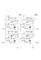
図1は、本実施形態のトランジスタ基板1000の平面例を示す。図2は、図1におけるI−I線断面を示す。トランジスタ基板1000は、基板1002と、該基板1002に設けられた有機半導体装置1003とを備える。有機半導体装置1003は、基板1002に所定の層が積層されて形成される。 FIG. 1 shows a plan example of a
本実施形態における基板1002は、一対の主面を有する。以下、「一方の主面」を、単に主面1004という場合がある。基板1002は、有機半導体装置1003を形成できる程度に機械的安定性、耐熱性および化学的安定性を有する限り、任意の材料によって構成されていてもよい。基板1002は、市販のもの、または公知の方法により製造されたものであってよい。基板1002は、たとえばプラスチック、シリコン、ガラス、これらが積層されたものであってもよい。 The
有機半導体装置1003は、導電膜1006と、絶縁膜1010と、活性層1012と、一対の入出力電極1014とを有する。導電膜1006は、例えば、基板1002の主面1004の上に形成され、活性層1012に電界を印加するゲート電極として機能する。導電膜1006は、求められる導電性が確保できる膜厚を有すればよい。 The
導電膜1006は、無機酸化物薄膜および金属薄膜などの無機導電膜、ならびに有機導電膜を用いて形成できる。導電膜1006の材料としては、たとえば透光性のインジウムスズ酸化物(ITO)、インジウム亜鉛酸化物(IZO)、インジウムタングステン酸化物(IWO)、アルミニウムドープ酸化亜鉛(AZO)、ガリウムドープ酸化亜鉛(GZO)、フッ素ドープ酸化亜鉛(FZO)、アンチモンドープ二酸化スズ(ATO)、フッ素ドープ二酸化スズ(FTO)、酸化マグネシウム(MgO)などの透光性導電体が例示できる。このように透光性導電体を導電膜1006として用いることにより、透光性の有機半導体装置1003を実現することもできるが、透光性の装置が求められていない場合には、透光性を示す導電体により導電膜1006を構成する必要はなく、遮光性の無機酸化物薄膜および金属薄膜などの無機導電膜、ならびに有機導電膜により導電膜を構成してもよい。 The
図1に示されるように、有機半導体装置1003は、導電膜1006の電気的接点として機能する接続部1008をさらに有する。該接続部1008は、基板1002の厚み方向から見て導電膜1006に重なる位置において活性層1012の表面上に形成される。活性層1012および後述する絶縁膜1010には、厚み方向に貫通して形成される導体柱(ビア)が設けられ、該導体柱によって接続部1008と導電膜1006とが電気的に接続される。 As shown in FIG. 1, the
接続部1008は、例えば、外部の他の電子部品などとの接続に用いられるボンディングワイヤが接続できる大きさを有すればよい。導電膜1006は、例えば、導体柱、接続部1008およびボンディングワイヤを介して外部回路と接続される。接続部1008および導体柱は、無機酸化物薄膜および金属薄膜などの無機導電膜、ならびに有機導電膜を用いて形成できる。 For example, the
有機半導体装置1003は、絶縁膜1010をさらに有する。該絶縁膜1010は、例えば、導電膜1006の上に形成され、本実施の形態では導電膜1006を覆って形成されている。すなわち導電膜1006は、基板1002と絶縁膜1010とにより囲繞されている。絶縁膜1010は、導電膜1006と一対の入出力電極1014とを電気的に絶縁できる限り、任意の材料によって構成されていてもよい。絶縁膜1010は、たとえば酸化珪素、窒化珪素、ポリイミド、ポリエチレン、ポリパラキシリレン(パリレン)、酸化アルミニウム、スピンオングラスなどの反応性有機シラン化合物などの周知の材料を積層することにより形成できる。絶縁膜1010は、たとえば50nm〜500nm程度の膜厚を有する。 The
活性層1012は、絶縁膜1010の基板1002側の表面とは反対側の表面上に形成される。活性層1012の厚みは、例えば、約150nm〜約5nmであってよい。活性層1012は、共役ポリマーを有する。共役ポリマーは、ポリマー主鎖の一部又は全部に非局在化したπ電子系を有するポリマーであり、共役した二重結合、三重結合及び/または芳香族環を有していてもよい。 The
分子量が小さすぎる場合にはクラックの発生等成膜性が悪化し実用性に乏しくなり、また分子量が大きすぎる場合には、有機溶媒への溶解性が悪くなり、溶液の粘度が高くなって塗布が困難になることがありうるので、重合体の好ましい分子量はポリスチレン換算数平均分子量で1000以上であり、より好ましくは2000〜500000である。また共役ポリマーとして、室温での移動度が1×10⁻³cm2/Vs以上のものを用いてもよく、イオン化ポテンシャルが4.7eV以上5.5eV以下のものを用いてもよい。When the molecular weight is too small, the film formability such as cracking is deteriorated and the practicality is poor, and when the molecular weight is too large, the solubility in an organic solvent is deteriorated, and the viscosity of the solution is increased and applied. Therefore, the preferred molecular weight of the polymer is 1000 or more in terms of polystyrene-equivalent number average molecular weight, and more preferably 2000 to 500,000. As the conjugated polymer, those having a mobility at room temperature of 1 × 10⁻³ cm2 / Vs or more may be used, and those having an ionization potential of 4.7 eV or more and 5.5 eV or less may be used.
共役ポリマーとして、ポリ−フルオレンもしくはその誘導体、または、置換もしくは無置換のフルオレンジイル基を繰り返し単位の1種として含む共重合体を用いてよい。共役ポリマーとして、ポリ−アリーレンもしくはその誘導体、または、置換もしくは無置換のアリーレン基を繰り返し単位の1種として含む共重合体を用いてよい。共役ポリマーとしては、フルオレン−チオフェン コポリマーが好ましく、フルオレン−チオフェン コポリマーとしては、ポリ(9,9'ジオクチルフルオレン−コ−ビチオフェン)(略称「F8T2」)が特に好ましい。 As the conjugated polymer, poly-fluorene or a derivative thereof, or a copolymer containing a substituted or unsubstituted fluorenediyl group as one kind of repeating unit may be used. As the conjugated polymer, poly-arylene or a derivative thereof, or a copolymer containing a substituted or unsubstituted arylene group as one kind of repeating unit may be used. The conjugated polymer is preferably a fluorene-thiophene copolymer, and the fluorene-thiophene copolymer is particularly preferably poly (9,9′dioctylfluorene-co-bithiophene) (abbreviation “F8T2”).
共役ポリマーとして、ポリ−アリーレンビニレンもしくはその誘導体、または、ポリ−チオフェンもしくはその誘導体等を用いてよい。共役ポリマーとして、ポリ−アニリンもしくはその誘導体、または、ポリ−ピロールもしくはその誘導体等を用いてよい。共役ポリマーとして、ポリ−2,5−チエニレンビニレンもしくはその誘導体、または、ポリビニルカルバゾールもしくはその誘導体等を用いてもよい。共役ポリマーとして、ポリ−シランもしくはその誘導体、または、側鎖もしくは主鎖に芳香族アミンを有するポリ−シロキサンの誘導体等を用いてよい。共役ポリマーとして、芳香族アミンの誘導体の(共)重合体等を用いてよい。 As the conjugated polymer, poly-arylene vinylene or a derivative thereof, poly-thiophene or a derivative thereof, or the like may be used. As the conjugated polymer, poly-aniline or a derivative thereof, poly-pyrrole or a derivative thereof, or the like may be used. As the conjugated polymer, poly-2,5-thienylene vinylene or a derivative thereof, polyvinyl carbazole or a derivative thereof, or the like may be used. As the conjugated polymer, poly-silane or a derivative thereof, or a poly-siloxane derivative having an aromatic amine in a side chain or a main chain may be used. As the conjugated polymer, a (co) polymer of an aromatic amine derivative or the like may be used.
共役ポリマーとして、ポリ−3−ヘキシルチオフェン(P3HT)、ポリ−3−オクチルチオフェンなどのポリ−3−アルキルチオフェン、ポリ−2,5− チエニレンビニレン(PTV)などを用いてもよい。共役ポリマーとして、ポリ−パラ−フェニレンビニレン(PPV)、ポリ−9,9−ジオクチルフルオレン(PFO)、ポリ−9,9−ジオクチルフルオレン−コ−ビス−N,N'−4−メトキシフェニル−ビス−N,N'−フェニル−1,4−フェニレンジアミン(PFMO)などを用いてもよい。共役ポリマーとして、ポリ−9,9−ジオクチルフルオレン−コ−ベンゾチアジアゾール(BT)、フルオレン−トリアリルアミン共重合体、トリアリルアミン系ポリマーなどを用いてもよい。 As the conjugated polymer, poly-3-alkylthiophene such as poly-3-hexylthiophene (P3HT) or poly-3-octylthiophene, poly-2,5-thienylene vinylene (PTV), or the like may be used. As conjugated polymers, poly-para-phenylene vinylene (PPV), poly-9,9-dioctylfluorene (PFO), poly-9,9-dioctylfluorene-co-bis-N, N′-4-methoxyphenyl-bis -N, N'-phenyl-1,4-phenylenediamine (PFMO) or the like may be used. As the conjugated polymer, poly-9,9-dioctylfluorene-co-benzothiadiazole (BT), fluorene-triallylamine copolymer, triallylamine-based polymer, or the like may be used.
一対の入出力電極1014は、例えば、活性層1012の絶縁膜1010側とは反対側の表面に接して設けられる。一対の入出力電極1014は、一方がソース電極として機能して、他方がドレイン電極として機能する。各入出力電極1014は、それぞれがソース電極、ドレイン電極として機能できるような形状に形成されていれば、その形状は特に限定されないが、本実施の形態では所定の方向(以下、チャネル幅方向という場合がある)に延伸して形成され、相対して略平行に配置される。 The pair of input /
本実施の形態における有機半導体装置1003は、入出力電極1014の電気的接点として機能する取出し電極部をさらに有する。この取出し電極部は、入出力電極1014と同一平面上に設けられ、入出力電極1014の中央部から延伸する取出し配線1020と、該取出し配線1020の端部に連接して形成される電極パッド1015とからなる。なお取出し電極部と入出力電極1014とは一体形成されている。この電極パッド1015は、例えば外部の他の電子部品などとの接続に用いられるボンディングワイヤが接続できる大きさを有すればよい。入出力電極1014は、取出し配線1020、電極パッド1015およびボンディングワイヤを介して外部回路と接続される。 The
一対の入出力電極1014および取出し電極部は、活性層1012に接して設けられるオーミック層1016と、該オーミック層1016に接して設けられる導電層1018とを有する。一対の入出力電極1014の間に、チャネルが形成される。チャネル長L1およびチャネル幅L2は、それぞれ所期の特性に応じて適宜設定される。チャネル長L1は、20μm〜120μm程度であり、チャネル幅L2は数十μm〜数mm程度である。入出力電極1014は、それぞれ、チャネル幅方向の距離L4が通常数十μm〜数mm程度であり、チャネル長方向の距離L3が通常数μm〜数百μmである。 The pair of input /
オーミック層1016は、活性層1012に接して形成される。オーミック層1016は、導電層1018と活性層1012との接触抵抗に比べると、活性層1012との接触抵抗が小さい部材によって構成され、電荷移動錯体または電子受容性有機分子を有することが好ましい。オーミック層1016の膜厚は、1nm以上10nm以下であってよい。これにより、取出し抵抗の増加をさらに抑制できる。オーミック層1016が1nm程度の膜厚を有することにより、活性層1012の表面を修飾できる。オーミック層1016の膜厚が10nmより大きくなると、取出し抵抗の増加を抑制しにくくなる。 The
オーミック層1016が電荷移動錯体を有する場合は、電荷移動錯体としてテトラシアノキノジメタン(TCNQ)に電子供与性分子テトラチアフルバレン(TTF)を組み合わせた電荷移動錯体テトラチアフルバレン−テトラシアノキノジメタン(TTF−TCNQ)を用いるとよい。電荷移動錯体としてTTF−TCNQの類似物質を用いてもよい。電荷移動錯体としてジベンゼンテトラチアフルバレン(DBTTF)に電子供与性分子テトラフルオロテトラシアノキノジメタン(F4TCNQ)を組み合わせた電荷移動錯体ジベンゾテトラチアフルバレン−テトラフルオロテトラシアノキノジメタン(DBTTF−F4TCNQ)、DBTTF−F4TCNQの類似物質を用いてもよい。When the
オーミック層1016が電子受容性有機分子を有する場合は、電子受容性有機分子としてテトラフルオロテトラシアノキノジメタン(F4TCNQ)を用いるとよい。F4TCNQは、強い電子受容性を有する。電子受容性有機分子として7,7,8,8−テトラシアノキノジメタン(TCNQ)などのキノジメタン誘導体、テトラシアノエチレン(TCNE)、ヘキサシアノブタジエン(HCNB)などのエチレン誘導体を用いてもよい。電子受容性有機分子としてジシクロジシアノベンゾキノン(DDQ)などのシアノ基を有する化合物、トリニトロフルオレノン(TNF)、ジニトロフルオレノン(DNF)などのニトロ基を有する化合物、フルオラニル、ブロマニルなどの有機材料を用いてもよい。電子受容性有機分子としてチオピラニリジン、その誘導体、ポリニトロフルオレノン、その誘導体、テトラシアノエチレン(TCNE)、その誘導体、クロラニル、その誘導体、2−4−1−メチルエチル−フェニル−6−フェニル−4H−チオピラン−4−イリデン−プロパンジニトリル−1,1−ジオキシイド(PTYPD)を用いてもよい。When the
電子受容性有機分子として2,4,7−トリニトロフルオレノン、カルボキシルフルオレノンマロニトリル(CFM)、その誘導体、N,N'ビス−ジアルキル−1,4,5,8−ナフタレンテトラカルボキシリックジイミド、その誘導体、N,N'ビス−ジアリール−1,4,5,8−ナフタレンテトラカルボキシリックジイミド、その誘導体、カルボキシベンジルナフタキノン、その誘導体、ジフェノキノン、その誘導体、フラーレン、その誘導体、11,11,12,12−テトラシアノナフト−2,6−キノジメタン(TNAP)、ヘキサクロロフタジェン(HCBD)、ヘキサシアノトリメチレンシクロプロパンド(HCTMCP)、テトラシアノキノキナゾリン(TCQQ)、フッ化リン錯体シクロペンタン鉄誘導体、ポリスチレンサルフォネート(PSS)を用いてもよい。活性層1012と一対の入出力電極1014との接触抵抗は、一対の入出力電極1014がオーミック層1016を有することにより低くなる。接触抵抗を低くすることにより、一対の入出力電極1014の取出し抵抗を低下できる。 2,4,7-trinitrofluorenone, carboxyl fluorenone malonitrile (CFM), derivatives thereof, N, N′bis-dialkyl-1,4,5,8-naphthalenetetracarboxylic diimide, Derivatives, N, N′bis-diaryl-1,4,5,8-naphthalenetetracarboxylic diimide, derivatives thereof, carboxybenzylnaphthaquinone, derivatives thereof, diphenoquinone, derivatives thereof, fullerenes, derivatives thereof, 11, 11, 12 , 12-tetracyanonaphth-2,6-quinodimethane (TNAP), hexachlorophthalene (HCBD), hexacyanotrimethylenecyclopropand (HCTMCP), tetracyanoquinoquinazoline (TCQQ), phosphorus fluoride complex cyclopentane iron derivative, Police Sarufoneto (PSS) may be used. The contact resistance between the
導電層1018は、オーミック層1016の上に形成され、好ましくはオーミック層1016と略同一のパターンで形成される。例えば、オーミック層1016と同一のマスクを用いて、導電層1018を形成してよい。これによりオーミック層1016の表面に垂直な方向から見て、導電層1018をオーミック層1016と略同一のパターンに形成することができる。導電層1018は、少なくとも電気抵抗率がオーミック層1016よりも高く又は電気抵抗率がオーミック層1016より低く、求められる導電性が確保でき、かつ加工が容易である膜厚を有すればよい。 The
活性層1012に接してオーミック層1016を設けることにより、接触抵抗を低くすることができるが、このオーミック層1016のみから入出力電極が構成されている従来の有機半導体装置では、チャネル幅方向の電気抵抗が高く、例えばチャネル幅方向の端部から、取出し配線1020が接続される中央部までに生じる電圧降下がおおきくなるところ、本実施の形態ではオーミック層1016に積層される導電層1018を設けることにより、入出力電極1014の電気抵抗をさらに低くすることができ、チャネル幅方向の電気抵抗を小さくすることができる。これによって入出力電極1014の取出し抵抗を低くすることができる。 By providing the
導電層1018は、無機系薄膜であることが好ましく、無機酸化物薄膜、金属薄膜を挙げることができる。無機酸化物薄膜としては、ITO(インジウムスズ酸化物)、IZO(インジウム亜鉛酸化物)などを挙げることができる。金属薄膜としては、Au、Ag、Al、Cr、Pt、Pd、Fe、Cu、Ni、TiおよびMoからなる群から選ばれる1種類以上の金属を含む薄膜を挙げることができる。導電層1018は、有機導電膜であってもよい。 The
一対の入出力電極1014が導電層1018を有することにより、一対の入出力電極1014のシート抵抗が低下する。これにより、一対の入出力電極1014の取出し抵抗が低下する。その結果、有機半導体装置1003が導通状態のときの抵抗を低減でき、ひいてはトランジスタ基板1000の消費電力を低減できる。 When the pair of input /
発光装置に備わる発光素子の駆動用トランジスタにトランジスタ基板1000を適用した場合は、発光装置の消費電力を低減できる。表示装置に備わる画素の駆動用トランジスタまたは選択用トランジスタにトランジスタ基板1000を適用することで、選択用トランジスタまたは駆動用トランジスタと信号ラインとの間の抵抗、および、選択用トランジスタと駆動用トランジスタとの間の抵抗を低減できる。これにより、信号ラインの走査速度を向上できる。信号ラインの走査速度が向上すると、トランジスタ基板1000は、大画面の表示装置に好適に用いることができる。 In the case where the
駆動用トランジスタまたは選択用トランジスタとしてトップゲート型のトランジスタを作製した場合には、トランジスタの共通ソースラインを信号ラインの一部として用いて、共通ソースラインを入出力電極1014と同様の構成を採用してよい。これにより、上記信号ラインの抵抗を低減でき、信号ラインの走査速度を向上できる。 When a top-gate transistor is manufactured as the driving transistor or the selection transistor, the common source line of the transistor is used as part of the signal line, and the common source line has a structure similar to that of the input /
図3〜図10は、トランジスタ基板1000の製造工程における断面例を示す。図3に示すように、基板1002を準備して、基板1002の主面1004の側に複数の導電膜1006を形成する。たとえば、表示装置に備わる画素の駆動用トランジスタまたは選択用トランジスタにトランジスタ基板1000を適用する場合は、各導電膜1006は各画素に対応して形成される。導電膜1006の形成方法として、たとえば、基板1002の主面1004の全面に導電層を積層して、積層後にフォトリソグラフィ法およびエッチング法を用いて加工する方法が例示できる。 3 to 10 show cross-sectional examples in the manufacturing process of the
次に導電膜1006を覆って絶縁膜1010を形成する。なお、本明細書において「上に形成する」とは、積層方向の一方(本実施形態では、「基板1002の厚み方向の一方」と同一)に形成されることを意味する。積層方向は、基板1002の主面1004に略垂直な方向であってよい。また、接して形成される場合だけでなく、別の層を介して形成される場合をも含む。図4に示すように、導電膜1006の上に、例えば塗布法を用いて絶縁膜1010の材料を堆積する。 Next, an insulating
以後の製作工程は、図4に符号Aで示す1つの素子に注目して説明する。図5に示すように、導電膜1006を形成して、その上に、例えば、塗布法およびフォトリソグラフィ法を用いて絶縁膜1010をパターニングすることにより、導電膜1006の上に絶縁膜1010を形成する。 The subsequent manufacturing process will be described by paying attention to one element indicated by symbol A in FIG. As shown in FIG. 5, the
次に、絶縁膜1010の上に活性層1012を形成する。活性層1012は、共役ポリマーを有する。共役ポリマーは、通常、有機溶媒などの溶媒に可溶なので、塗布法により形成できる。塗布法により形成すると、製造工程を簡略化できる。塗布法は、スリットコーティング法、ノズルコーティング法、インクジェット法、キャスティング法、マイクログラビアコート法、グラビアコート法、バーコート法、ロールコート法、ワイアーバーコート法、ディップコート法、スプレーコート法、スクリーン印刷法、フレキソ印刷法、またはオフセット印刷法などが例示できる。 Next, an
例えばスピンコーティング法を用いて活性層1012を形成する場合には、図6に示すように、共役ポリマーを含む活性層1012の材料インク5010をノズル5000から滴下するとともに、基板1002を回転させることで、絶縁膜1010の表面上にインクから成る薄膜5012を形成して、さらに乾燥させることで活性層1012を形成することができる。また例えばエッチング法を用いて活性層1012をパターニングしてもよい。 For example, when the
図8に示すように、メタルシャドウマスク7000を活性層1012上に配置して、オーミック層1016および導電層1018が形成される範囲を画定する。図9に示すように、メタルシャドウマスク7000を用いて画定された範囲に、たとえば真空蒸着法を用いてオーミック層1016を積層する。オーミック層1016は、キャスト法またはスタンプ法を用いて形成してもよい。 As shown in FIG. 8, a
図10に示すように、オーミック層1016を形成する段階で用いたメタルシャドウマスク7000で範囲を画定したまま、オーミック層1016と略同じパターンの導電層1018を積層する。このようにオーミック層1016と導電層1018との形状を略同一のパターンに設計することで、オーミック層1016の形成に用いるメタルシャドウマスクを、導電層1018の形成に用いるメタルシャドウマスクにそのまま転用することができ、これによってメタルシャドウマスクの枚数を削減することができる。 As shown in FIG. 10, a
さらにオーミック層1016を形成する段階で用いたメタルシャドウマスク7000で範囲を画定したまま、オーミック層1016と略同じパターンの導電層1018を積層するので、オーミック層1016を形成する段階でメタルシャドウマスクの位置合わせを省略することができ、これにより、工程を簡略化することができる。なお一対の入出力電極1014または取出し電極部として機能するオーミック層1016および導電層1018は、一対の入出力電極1014または取出し電極部として機能する部分が同一の工程で形成される。導電層1018の形成方法として、スパッタリング法、CVD法、蒸着法が例示できる。 Further, since the
導電膜1006の上に接続部1008を形成する。接続部1008は、メタルシャドウマスクを用いた蒸着により形成してもよく、リフトオフ法を用いた蒸着により形成してもよい。以上のようにして、本実施形態のトランジスタ基板1000を製造できる。 A
本実施形態では、トランジスタ基板1000の一例を説明した。他の実施形態として、耐熱性を有する基板1002に形成した有機半導体装置を、可撓性を有する基板1002へ転写することにより製造されるトランジスタ基板1000の例が挙げられる。 In this embodiment, an example of the
図11は、本実施形態のトランジスタ基板1000を適用する表示装置の回路例を示す。なお、図11において、符号に「11」、「12」などの2桁の数字を含む場合、当該数字は行列配置された部材の行番号および列番号を示す。これら行列配置された部材は同一のものであり、行位置および列位置を特定しない場合には、2桁の数字の前部で特定される符号で代表する。たとえば発光セルC11、発光セルC12、発光セルC21、発光セルC22を区別しない場合は、単に発光セルCと記載する。 FIG. 11 shows a circuit example of a display device to which the
図11に示す表示装置は、画素と、該画素に電気的に結合され、該画素を制御する有機半導体装置1003とを備える。具体的には、表示装置は、発光セルC11、発光セルC12、発光セルC21、発光セルC22を備える。 The display device illustrated in FIG. 11 includes a pixel and an
発光セルCは、例えば、行方向および列方向のマトリックス状に配置される。マトリックス状に配置された発光セルCはデータ線DLおよびゲート線GLによって選択される。たとえばデータ線DL1とゲート線GL1が選択されている場合は、発光セルC11が発光する。 The light emitting cells C are arranged in a matrix in the row direction and the column direction, for example. The light emitting cells C arranged in a matrix are selected by the data line DL and the gate line GL. For example, when the data line DL1 and the gate line GL1 are selected, the light emitting cell C11 emits light.
発光セルCは、有機半導体装置1003に相当するスイッチトランジスタTrsと、有機半導体装置1003に相当する駆動トランジスタTrdと、画素に相当する発光素子PLと、キャパシタCpを有してよい。本実施形態では、例えば、スイッチトランジスタTrsは、ゲート端子がゲート線GLに接続され、ソース端子がデータ線DLに接続される。スイッチトランジスタTrsのドレイン端子は、駆動トランジスタTrdのゲート端子に接続される。スイッチトランジスタTrsのドレイン端子は、キャパシタCpを介して、接地線GNDに接続される。駆動トランジスタTrdのソース端子は、発光素子PLの一方の端子に接続される。発光素子PLの他方の端子は、電源線VDDに接続される。駆動トランジスタTrdのドレイン端子は、接地線GNDに接続される。The light emitting cell C may include a switch transistor Trs corresponding to the
これにより、スイッチトランジスタTrsがONのときのデータ線DLの電位に対応する電化がキャパシタCpに蓄積される。キャパシタCpに蓄積された電荷に応じて駆動トランジスタTrdのソース/ドレイン間の抵抗が制御され、キャパシタCpに蓄積された電荷に応じた輝度で発光素子PLが発光する。画素に相当する発光素子PLは、例えば高分子または低分子の有機エレクトロルミネッセンス素子(以下、有機EL素子という場合がある)および無機EL素子などの自発光型の発光素子によって実現される。このように有機半導体装置により画素(発光素子PL)の発光が制御され、これによって画素(発光素子PL)の表示が制御される。 Thereby, electrification corresponding to the potential of the data line DL when the switch transistor Trs is ON is accumulated in the capacitor Cp. The resistance between the source and the drain of the drive transistor Trd is controlled according to the electric charge accumulated in the capacitor Cp, and the light emitting element PL emits light with the luminance corresponding to the electric charge accumulated in the capacitor Cp. The light-emitting element PL corresponding to a pixel is realized by a self-luminous light-emitting element such as a polymer or low-molecular organic electroluminescence element (hereinafter sometimes referred to as an organic EL element) and an inorganic EL element. In this way, the light emission of the pixel (light emitting element PL) is controlled by the organic semiconductor device, and thereby the display of the pixel (light emitting element PL) is controlled.
表示装置の他の実施形態として、液晶表示装置が挙げられる。液晶表示装置は、図11に記載の発光表示装置と同様に、画素に相当する液晶セルと、該液晶セルに電気的に結合され、該液晶セルの表示を制御する前述の実施の形態の有機半導体装置などを備え、液晶セルCは行方向および列方向のマトリックス状に配置される。液晶セルの表示を制御するとは、液晶セルに印加電圧を印加するか否かを有機半導体装置が選択的に切替えることにより、バックライトから液晶セルに照射される光を透過させるか否かを選択的に切替えることを意味する。液晶セルをさらに多数備えてもよい点、マトリックス配置された液晶セルがデータ線DLおよびゲート線GLによって選択される点は、図11に示す表示装置と同様であってよい。 Another embodiment of the display device is a liquid crystal display device. Similar to the light-emitting display device shown in FIG. 11, the liquid crystal display device includes a liquid crystal cell corresponding to a pixel, and the organic display of the above-described embodiment that is electrically coupled to the liquid crystal cell and controls the display of the liquid crystal cell. A liquid crystal cell C is provided in a matrix in the row direction and the column direction. Controlling the display of the liquid crystal cell means whether or not the light applied to the liquid crystal cell from the backlight is transmitted by selectively switching whether or not the applied voltage is applied to the liquid crystal cell. Means switching automatically. The display device shown in FIG. 11 may be the same as the display device shown in FIG. 11 in that a larger number of liquid crystal cells may be provided and the liquid crystal cells arranged in matrix are selected by the data lines DL and the gate lines GL.
本実施形態のトランジスタ基板1000を適用する発光装置は、例えば図11に示す表示装置と同様の回路構成を有していてもよい。発光装置は、発光素子と、該発光素子に電気的に結合され、該発光素子の発光を制御する有機半導体装置1003を備える。 A light emitting device to which the
(実施例1)
図3から図10に示された手順に従って、基板1002の上に、導電膜1006と、絶縁膜1010と、活性層1012と、一対の入出力電極1014とを備えるトランジスタ基板1000を製造した。基板1002としてガラス基板を準備した。基板1002の主面1004の側にスパッタリング法を用いてクロム膜を積層して、積層したクロム膜をフォトリソグラフィー法によりパターニングして、複数の導電膜1006を形成した。導電膜1006の上に、スピンオングラス膜を形成して絶縁膜1010とした。スピンオングラス膜は、スピンコート法により塗布した後、加熱処理をすることで形成した。Example 1
A
絶縁膜1010の上に、スピンコート法を用いてノズル5000からフルオレン−チオフェン コポリマーであるポリ(9,9'ジオクチルフルオレン−コ−ビチオフェン)(略称「F8T2」)を含む溶液を供給して、膜厚が80nmになるように活性層1012を形成した。活性層1012の上をメタルシャドウマスク7000で覆って一対の入出力電極1014を形成する範囲を画定しながら、真空蒸着法を用いて電荷移動錯体テトラチアフルバレン−テトラシアノキノジメタン(TTF−TCNQ)を積層して、膜厚が10nmになるようにオーミック層1016を形成した。活性層1012の上をメタルシャドウマスク7000で覆ったまま、真空蒸着法を用いてAuを40nm積層して、オーミック層1016と略同じパターンの導電層1018を形成した。導電膜1006の上の活性層1012および絶縁膜1010の一部を除去してAgペーストを塗布して接続部1008を形成した(図1参照)。 A solution containing poly (9,9′dioctylfluorene-co-bithiophene) (abbreviation “F8T2”), which is a fluorene-thiophene copolymer, is supplied onto the insulating
(実施例2)
オーミック層1016の形成以外の製造条件を実施例1と同様にしてトランジスタ基板1000を製造した。活性層1012の上をメタルシャドウマスク7000で覆ってオーミック層1016を形成する範囲を画定しながら、真空蒸着法を用いてテトラフルオロテトラシアノキノジメタン(F4TCNQ)を積層して、膜厚が5nmになるようにオーミック層1016を形成した。(Example 2)
A
(比較例)
比較例として、オーミック層がないトランジスタ基板を製造した。製造条件は、オーミック層の形成以外は実施例1と同様にした。活性層1012の上をメタルシャドウマスク7000で覆って一対の入出力電極1014を形成する範囲を画定しながら、真空蒸着法を用いてAuを40nm積層して導電層1018を形成した。(Comparative example)
As a comparative example, a transistor substrate without an ohmic layer was manufactured. The manufacturing conditions were the same as in Example 1 except for the formation of the ohmic layer. The
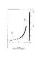
図12は、実施例1のトランジスタ基板1000の一対の入出力電極1014について、取出し抵抗を評価した結果を示す。図12の横軸は、入出力電極間の電流Id[A]を示す。図12の縦軸は、単位幅当りの入出力電極の取出し抵抗[Ωcm]を示す。図12の符号1202は、実施例1の評価結果を示す。また、符号1204は、比較例の評価結果を示す。上記評価には、チャネル幅L2が2mmであり、チャネル長L1がそれぞれ20μm、30μm、40μm、80μm,120μmである5種類の入出力電極1014を備えるトランジスタを用いた。また入出力電極1014と電極パッド1015とを接続する取出し配線1020は、チャネル長方向の距離L3が100μmであり、チャネル幅方向の距離L4が1840μm〜1890μmである。取出し抵抗の評価には、gated−TLM法を用いた。図12に示す通り、実施例1のトランジスタ基板の一対の入出力電極1014の取出し抵抗の値は、比較例と比較して半分程度に低下した。 FIG. 12 shows the results of evaluating the take-out resistance of the pair of input /
図13は、実施例2のトランジスタ基板1000の一対の入出力電極1014について、取出し抵抗を評価した結果を示す。図13の横軸は、横軸は入出力電極間の電流Id[A]を示す。図13の縦軸は、単位幅当りの入出力電極の取出し抵抗[Ωcm]を示す。図13の符号1302は、実施例2の評価結果を示す。また、符号1204は、比較例の評価結果を示す。取出し抵抗は、図12の場合と同様にして評価した。図13に示す通り、実施例2のトランジスタ基板の一対の入出力電極1014の取出し抵抗値は、比較例と比較して大幅に低下した。特に、低電流領域における取出し抵抗の増加がなく、いわゆるオーミック特性を示した。 FIG. 13 shows the result of evaluating the take-out resistance of the pair of input /
以上、本発明を実施の形態を用いて説明したが、本発明の技術的範囲は上記実施の形態に記載の範囲には限定されない。上記実施の形態に、多様な変更または改良を加えることが可能であることが当業者に明らかである。その様な変更または改良を加えた形態も本発明の技術的範囲に含まれ得ることが、特許請求の範囲の記載から明らかである。 As mentioned above, although this invention was demonstrated using embodiment, the technical scope of this invention is not limited to the range as described in the said embodiment. It will be apparent to those skilled in the art that various modifications or improvements can be added to the above-described embodiment. It is apparent from the scope of the claims that the embodiments added with such changes or improvements can be included in the technical scope of the present invention.
特許請求の範囲、明細書、および図面中において示した装置、システム、プログラム、および方法における動作、手順、ステップ、および段階等の各処理の実行順序は、特段「より前に」、「先立って」等と明示しておらず、また、前の処理の出力を後の処理で用いるのでない限り、任意の順序で実現しうることに留意すべきである。特許請求の範囲、明細書、および図面中の動作フローに関して、便宜上「まず、」、「次に、」等を用いて説明したとしても、この順で実施することが必須であることを意味するものではない。 The order of execution of each process such as operations, procedures, steps, and stages in the apparatus, system, program, and method shown in the claims, the description, and the drawings is particularly “before” or “prior to”. It should be noted that the output can be realized in any order unless the output of the previous process is used in the subsequent process. Regarding the operation flow in the claims, the description, and the drawings, even if it is described using “first”, “next”, etc. for convenience, it means that it is essential to carry out in this order. It is not a thing.
1000 トランジスタ基板
1002 基板
1003 有機半導体装置
1004 主面
1006 導電膜
1008 接続部
1010 絶縁膜
1012 活性層
1014 入出力電極
1015 電極パッド
1016 オーミック層
1018 導電層
1020 取出し配線
5000 ノズル
5010 材料インク
5012 薄膜
7000 メタルシャドウマスク1000
Claims (11)
Translated fromJapanese前記活性層に接する一対の入出力電極と、
を備え、
前記一対の入出力電極の少なくとも一方は、前記活性層に接するオーミック層と、前記オーミック層に接する導電層とを有する有機半導体装置。An active layer having a conjugated polymer;
A pair of input / output electrodes in contact with the active layer;
With
At least one of the pair of input / output electrodes is an organic semiconductor device having an ohmic layer in contact with the active layer and a conductive layer in contact with the ohmic layer.
請求項1に記載の有機半導体装置。The conductive layer and the ohmic layer have substantially the same pattern as viewed from a direction perpendicular to the interface between the conductive layer and the ohmic layer.
The organic semiconductor device according to claim 1.
請求項1または請求項2に記載の有機半導体装置。The ohmic layer has a charge transfer complex molecule or an electron accepting organic molecule,
The organic semiconductor device according to claim 1 or 2.
請求項1から請求項3のいずれか一項に記載の有機半導体装置。The ohmic layer has a thickness of 1 nm or more and 10 nm or less.
The organic-semiconductor device as described in any one of Claims 1-3.
請求項1から請求項4のいずれか一項に記載の有機半導体装置。The conjugated polymer is a fluorene-thiophene copolymer.
The organic-semiconductor device as described in any one of Claims 1-4.
前記活性層を準備する段階の後に、前記活性層の上にオーミック層を形成する段階と、
前記オーミック層を形成する段階の後に、前記活性層の上に導電層を形成する段階と、
を備える、有機半導体装置の製造方法。Providing an active layer having a conjugated polymer on a substrate;
After the step of preparing the active layer, forming an ohmic layer on the active layer;
After forming the ohmic layer, forming a conductive layer on the active layer;
A method for manufacturing an organic semiconductor device.
請求項6に記載の有機半導体装置の製造方法。In the step of forming the conductive layer, the conductive layer is formed in substantially the same pattern as the ohmic layer when viewed from a direction perpendicular to the surface of the ohmic layer.
The manufacturing method of the organic-semiconductor device of Claim 6.
請求項7に記載の有機半導体装置の製造方法。In the step of forming the ohmic layer and the step of forming the conductive layer, the same metal shadow mask is used.
The manufacturing method of the organic-semiconductor device of Claim 7.
前記基板に設けられた請求項1から請求項5の何れか1項に記載の有機半導体装置と、
を備えるトランジスタ基板。A substrate,
The organic semiconductor device according to any one of claims 1 to 5, provided on the substrate,
A transistor substrate comprising:
前記発光素子に電気的に結合され、前記発光素子の発光を制御する請求項1から請求項5の何れか1項に記載の有機半導体装置と、
を備える発光装置。A light emitting element;
The organic semiconductor device according to any one of claims 1 to 5, wherein the organic semiconductor device is electrically coupled to the light emitting element and controls light emission of the light emitting element.
A light emitting device comprising:
前記画素に電気的に結合され、前記画素の表示を制御する請求項1から請求項5の何れか1項に記載の有機半導体装置と、
を備える表示装置。Pixels,
The organic semiconductor device according to any one of claims 1 to 5, wherein the organic semiconductor device is electrically coupled to the pixel and controls display of the pixel.
A display device comprising:
Priority Applications (1)
| Application Number | Priority Date | Filing Date | Title |
|---|---|---|---|
| JP2008324679AJP2010147344A (en) | 2008-12-19 | 2008-12-19 | Organic semiconductor device and method of manufacturing the same |
Applications Claiming Priority (1)
| Application Number | Priority Date | Filing Date | Title |
|---|---|---|---|
| JP2008324679AJP2010147344A (en) | 2008-12-19 | 2008-12-19 | Organic semiconductor device and method of manufacturing the same |
Publications (1)
| Publication Number | Publication Date |
|---|---|
| JP2010147344Atrue JP2010147344A (en) | 2010-07-01 |
Family
ID=42567431
Family Applications (1)
| Application Number | Title | Priority Date | Filing Date |
|---|---|---|---|
| JP2008324679APendingJP2010147344A (en) | 2008-12-19 | 2008-12-19 | Organic semiconductor device and method of manufacturing the same |
Country Status (1)
| Country | Link |
|---|---|
| JP (1) | JP2010147344A (en) |
Cited By (1)
| Publication number | Priority date | Publication date | Assignee | Title |
|---|---|---|---|---|
| JP2013175571A (en)* | 2012-02-24 | 2013-09-05 | National Institute For Materials Science | Organic field effect transistor |
Citations (3)
| Publication number | Priority date | Publication date | Assignee | Title |
|---|---|---|---|---|
| JP2006059896A (en)* | 2004-08-18 | 2006-03-02 | Sony Corp | Field effect transistor |
| JP2007019291A (en)* | 2005-07-08 | 2007-01-25 | National Institute Of Advanced Industrial & Technology | Organic semiconductor device |
| JP2007227907A (en)* | 2006-01-26 | 2007-09-06 | Semiconductor Energy Lab Co Ltd | Organic field effect transistor and semiconductor device |
- 2008
- 2008-12-19JPJP2008324679Apatent/JP2010147344A/enactivePending
Patent Citations (3)
| Publication number | Priority date | Publication date | Assignee | Title |
|---|---|---|---|---|
| JP2006059896A (en)* | 2004-08-18 | 2006-03-02 | Sony Corp | Field effect transistor |
| JP2007019291A (en)* | 2005-07-08 | 2007-01-25 | National Institute Of Advanced Industrial & Technology | Organic semiconductor device |
| JP2007227907A (en)* | 2006-01-26 | 2007-09-06 | Semiconductor Energy Lab Co Ltd | Organic field effect transistor and semiconductor device |
Cited By (1)
| Publication number | Priority date | Publication date | Assignee | Title |
|---|---|---|---|---|
| JP2013175571A (en)* | 2012-02-24 | 2013-09-05 | National Institute For Materials Science | Organic field effect transistor |
Similar Documents
| Publication | Publication Date | Title |
|---|---|---|
| US10341475B2 (en) | Display unit, method of manufacturing the same, and electronic apparatus | |
| JP4504908B2 (en) | Thin film transistor and flat panel display using the same | |
| US8466459B2 (en) | Organic light emitting display device and method of manufacturing the same | |
| US20110198598A1 (en) | Organic light emitting display apparatus and method of manufacturing the same | |
| US20070024766A1 (en) | Organic thin film transistor display panel | |
| CN102194996B (en) | Thin-film transistor and electronic installation | |
| KR20110049578A (en) | Organic electroluminescent display | |
| CN103370776B (en) | Thin-film transistor element and manufacture method, organic EL display element and organic EL display | |
| US20110121301A1 (en) | Organic light emitting display device and method of manufacturing the same | |
| CN103000808A (en) | Thin-film transistor and electronic unit | |
| JP5770104B2 (en) | Method for forming source and drain electrodes of organic thin film transistor by electroless plating | |
| CN104078487B (en) | Display unit, the manufacture method of the display unit and electronic installation | |
| TWI373865B (en) | Organic thin film transistor array panel and manufacturing method thereof | |
| CN102142520B (en) | Thin-film transistor and manufacture method thereof and electronic installation | |
| WO2006098420A1 (en) | Light-emitting device and display | |
| CN106537565A (en) | Electronic device, method for manufacturing same, and electronic apparatus | |
| JP5132880B2 (en) | Organic thin film transistor array panel and manufacturing method thereof | |
| US7897216B2 (en) | Method for manufacturing organic device and electronic apparatus | |
| JP2010147344A (en) | Organic semiconductor device and method of manufacturing the same | |
| JP5264089B2 (en) | Semiconductor element, organic light emitting display device provided with the same, and method of manufacturing the semiconductor element | |
| KR100659112B1 (en) | Organic thin film transistor and manufacturing method thereof, flat display device having same | |
| KR100730183B1 (en) | Organic thin film transistor and manufacturing method thereof, flat display device having same | |
| JP2006098542A (en) | Organic electroluminescence apparatus | |
| EP2565954A2 (en) | Transistor and method of producing same, and display | |
| KR20080045845A (en) | Thin film transistor array panel and manufacturing method thereof |
Legal Events
| Date | Code | Title | Description |
|---|---|---|---|
| A621 | Written request for application examination | Free format text:JAPANESE INTERMEDIATE CODE: A621 Effective date:20110408 | |
| A977 | Report on retrieval | Free format text:JAPANESE INTERMEDIATE CODE: A971007 Effective date:20130423 | |
| A131 | Notification of reasons for refusal | Free format text:JAPANESE INTERMEDIATE CODE: A131 Effective date:20130430 | |
| A02 | Decision of refusal | Free format text:JAPANESE INTERMEDIATE CODE: A02 Effective date:20130903 |