JP2010129125A - Multivalue nonvolatile semiconductor memory - Google Patents
Multivalue nonvolatile semiconductor memoryDownload PDFInfo
- Publication number
- JP2010129125A JP2010129125AJP2008302758AJP2008302758AJP2010129125AJP 2010129125 AJP2010129125 AJP 2010129125AJP 2008302758 AJP2008302758 AJP 2008302758AJP 2008302758 AJP2008302758 AJP 2008302758AJP 2010129125 AJP2010129125 AJP 2010129125A
- Authority
- JP
- Japan
- Prior art keywords
- potential
- word line
- read
- memory cell
- select gate
- Prior art date
- Legal status (The legal status is an assumption and is not a legal conclusion. Google has not performed a legal analysis and makes no representation as to the accuracy of the status listed.)
- Pending
Links
Images


Classifications
- G—PHYSICS
- G11—INFORMATION STORAGE
- G11C—STATIC STORES
- G11C11/00—Digital stores characterised by the use of particular electric or magnetic storage elements; Storage elements therefor
- G11C11/56—Digital stores characterised by the use of particular electric or magnetic storage elements; Storage elements therefor using storage elements with more than two stable states represented by steps, e.g. of voltage, current, phase, frequency
- G11C11/5621—Digital stores characterised by the use of particular electric or magnetic storage elements; Storage elements therefor using storage elements with more than two stable states represented by steps, e.g. of voltage, current, phase, frequency using charge storage in a floating gate
- G11C11/5642—Sensing or reading circuits; Data output circuits
- G—PHYSICS
- G11—INFORMATION STORAGE
- G11C—STATIC STORES
- G11C16/00—Erasable programmable read-only memories
- G11C16/02—Erasable programmable read-only memories electrically programmable
- G11C16/04—Erasable programmable read-only memories electrically programmable using variable threshold transistors, e.g. FAMOS
- G11C16/0483—Erasable programmable read-only memories electrically programmable using variable threshold transistors, e.g. FAMOS comprising cells having several storage transistors connected in series
- G—PHYSICS
- G11—INFORMATION STORAGE
- G11C—STATIC STORES
- G11C2211/00—Indexing scheme relating to digital stores characterized by the use of particular electric or magnetic storage elements; Storage elements therefor
- G11C2211/56—Indexing scheme relating to G11C11/56 and sub-groups for features not covered by these groups
- G11C2211/562—Multilevel memory programming aspects
- G11C2211/5621—Multilevel programming verification
Landscapes
- Engineering & Computer Science (AREA)
- Microelectronics & Electronic Packaging (AREA)
- Computer Hardware Design (AREA)
- Read Only Memory (AREA)
Abstract
Translated fromJapaneseDescription
Translated fromJapanese本発明は、多値不揮発性半導体メモリの読み出し動作に関する。 The present invention relates to a read operation of a multi-value nonvolatile semiconductor memory.
複数のメモリセルにより一つのセルユニットが構成される不揮発性半導体メモリ、例えば、NANDフラッシュメモリ(例えば、特許文献1を参照)では、メモリセルアレイの高集積化が進むにつれて、一つのセルユニット内の複数のワード線の配線抵抗と、これら複数のワード線間の寄生容量とに起因するいくつかの問題が発生している。 In a nonvolatile semiconductor memory in which one cell unit is constituted by a plurality of memory cells, for example, a NAND flash memory (see, for example, Patent Document 1), as the memory cell array is highly integrated, Several problems are caused by the wiring resistance of the plurality of word lines and the parasitic capacitance between the plurality of word lines.
そのうちの一つに、読み出し時におけるワード線セットアップ期間の長期化がある。 One of them is the lengthening of the word line setup period during reading.
ここで、本明細書において、ワード線セットアップ期間とは、選択ワード線に選択読み出し電位を印加し始めてからセンスを開始するまでの期間のことである。 Here, in this specification, the word line setup period is a period from the start of applying a selective read potential to a selected word line until the start of sensing.
また、選択読み出し電位とは、読み出し対象となる選択メモリセルのデータに応じてそのメモリセルのオン/オフが決まる電位のことである。センスを開始するとは、ビット線の電位を選択メモリセルのデータに応じた値にし始めること、又は、センスアンプによりメモリセルのデータをセンスし始めることである。 The selected read potential is a potential that determines whether a memory cell is turned on or off according to data of the selected memory cell to be read. To start sensing means to start the potential of the bit line to a value corresponding to the data of the selected memory cell, or to start sensing the data of the memory cell by the sense amplifier.
さらに、単に読み出しと言ったときは、通常読み出しとベリファイ読み出しの双方を含むものとする。通常読み出しとは、チップ外部にメモリセルのデータを出力することであり、ベリファイ読み出しとは、書き込み時に正確にデータが書き込めたか否かを検証するための読み出しを行うことである。 Furthermore, when simply reading, it is assumed that both normal reading and verify reading are included. The normal reading is to output the data of the memory cell to the outside of the chip, and the verify reading is to perform reading for verifying whether or not the data has been correctly written at the time of writing.
メモリセルアレイの高集積化が進むと、一つのセルユニット内の複数のワード線は、細く、かつ、長くなり、配線抵抗が増大する。また、これら複数のワード線間の幅が狭くなり、寄生容量が増大する。 As the memory cell array is highly integrated, a plurality of word lines in one cell unit become thinner and longer, and the wiring resistance increases. Further, the width between the plurality of word lines is reduced, and the parasitic capacitance is increased.
このような状況の下では、非選択読み出し電位が、非選択ワード線の一端(ワード線ドライバに最も近い端部)から他端(ワード線ドライバに最も遠い端部)まで、完全に伝わるには一定時間を要する、即ち、非選択ワード線の他端の電位の立ち上がり波形が緩やかになる。 Under such circumstances, the non-selected read potential can be completely transmitted from one end of the non-selected word line (the end closest to the word line driver) to the other end (the end farthest from the word line driver). A certain time is required, that is, the rising waveform of the potential at the other end of the non-selected word line becomes gentle.
また、非選択読み出し電位は、読み出し対象とならない非選択メモリセルの閾値によらずそのメモリセルをオンにする電位のことであり、選択ワード線に印加する選択読み出し電位よりも大きい。 The non-selected read potential is a potential for turning on a memory cell regardless of the threshold value of the non-selected memory cell that is not a read target, and is higher than the selected read potential applied to the selected word line.
このため、非選択ワード線の他端の電位の立ち上がりに起因して、選択ワード線の他端の電位は、選択ワード線と隣接した非選択ワード線との容量カップリングにより、非選択読み出し電位付近まで上昇する。 For this reason, due to the rise of the potential at the other end of the non-selected word line, the potential at the other end of the selected word line is changed to the non-selected read potential by capacitive coupling between the selected word line and the adjacent non-selected word line. It rises to near.
また、上述のように、非選択ワード線の他端の電位の立ち上がり波形が緩やかなために、選択ワード線の一端に選択読み出し電位を印加した後においても、選択ワード線の他端の電位は、非選択ワード線の他端の電位の影響を受けて、非選択読み出し電位付近の電位を維持する。 As described above, since the rising waveform of the potential at the other end of the non-selected word line is gentle, the potential at the other end of the selected word line remains even after the selective read potential is applied to one end of the selected word line. The potential near the non-selected read potential is maintained under the influence of the potential at the other end of the non-selected word line.
従って、選択ワード線の電位が、非選択読み出し電位付近から低下し、最終的に選択読み出し電位に落ち着くまでには、非常に長い時間を要する。 Therefore, it takes a very long time for the potential of the selected word line to drop from the vicinity of the non-selected read potential and finally settle to the selected read potential.
一方で、センスの開始は、誤読み出しを防止するため、選択ワード線の他端の電位が、選択読み出し電位になってからでないと行うことはできない。 On the other hand, in order to prevent erroneous reading, the sense can be started only after the potential at the other end of the selected word line becomes the selected read potential.
このようなことから、ワード線セットアップ期間が長期化する。 For this reason, the word line setup period is prolonged.
特に、一つのメモリセルに三値以上を記憶させる多値不揮発性半導体メモリでは、選択ワード線に印加する選択読み出し電位の値は、二つ以上存在する。即ち、一つのメモリセルに記憶させるデータ数が大きくなるにつれて、非選択読み出し電位の値と選択読み出し電位の最も低い値との差が大きくなる。 In particular, in a multi-value nonvolatile semiconductor memory that stores three or more values in one memory cell, there are two or more values of the selected read potential applied to the selected word line. That is, as the number of data stored in one memory cell increases, the difference between the value of the non-selected read potential and the lowest value of the selected read potential increases.
このため、選択読み出し電位が最も低い値のとき、選択ワード線の他端の電位が、非選択読み出し電位付近から選択読み出し電位になるまでの期間が最も長くなる。 Therefore, when the selected read potential is the lowest value, the period until the potential at the other end of the selected word line becomes the selected read potential from the vicinity of the non-selected read potential is the longest.
また、ワード線セットアップ期間は、選択読み出し電位の値にかかわらず、上述の最も長い期間に固定される。 The word line setup period is fixed to the longest period described above regardless of the value of the selected read potential.
従って、多値不揮発性半導体メモリでは、メモリセルアレイの高集積化によるワード線セットアップ期間の長期化が特に顕著となる。 Therefore, in the multi-value nonvolatile semiconductor memory, the prolongation of the word line setup period due to the high integration of the memory cell array becomes particularly remarkable.
このようなワード線セットアップ期間の長期化は、読み出し動作の高速化の阻害要因となる。
本発明は、読み出し動作を高速化するためのワード線セットアップ期間の設定技術について提案する。 The present invention proposes a technique for setting a word line setup period for speeding up a read operation.
本発明の例に係る多値不揮発性半導体メモリは、第一及び第二セレクトゲートトランジスタと、前記第一及び第二セレクトゲートトランジスタの間に直列接続され、各々が三値以上を記憶する複数のメモリセルと、前記複数のメモリセルのうち読み出し対象となる選択メモリセルに接続される選択ワード線と、前記複数のメモリセルのうち前記選択メモリセル以外の非選択メモリセルに接続される非選択ワード線と、読み出し時に、前記選択ワード線に選択読み出し電位を印加し、前記非選択ワード線に前記選択読み出し電位よりも高い非選択読み出し電位を印加する電位発生回路と、異なる二つ以上の読み出し電位のうちの一つを前記選択読み出し電位とし、前記選択読み出し電位の値に応じてワード線セットアップ期間を異ならせる制御回路とを備える。 A multi-level nonvolatile semiconductor memory according to an example of the present invention includes a plurality of first and second select gate transistors and a plurality of ternary values each connected in series between the first and second select gate transistors. A memory cell; a selected word line connected to a selected memory cell to be read out of the plurality of memory cells; and a non-selected memory cell connected to a non-selected memory cell other than the selected memory cell among the plurality of memory cells. Two or more different readings from a word line and a potential generation circuit that applies a selected read potential to the selected word line and applies a non-selected read potential higher than the selected read potential to the non-selected word line at the time of reading. One of the potentials is set as the selected read potential, and the word line setup period is changed according to the value of the selected read potential. And a road.
本発明によれば、ワード線セットアップ期間の設定を工夫することにより読み出し動作を高速化できる。 According to the present invention, the read operation can be speeded up by devising the setting of the word line setup period.
以下、図面を参照しながら、本発明の例を実施するための最良の形態について詳細に説明する。 The best mode for carrying out an example of the present invention will be described below in detail with reference to the drawings.
1. 概要
本発明の例では、一つのメモリセルが三値以上を記憶する多値不揮発性半導体メモリにおいて、ワード線セットアップ期間を選択読み出し電位の値に応じて異ならせる。1. Overview
In the example of the present invention, in a multi-value nonvolatile semiconductor memory in which one memory cell stores three or more values, the word line setup period is varied according to the value of the selected read potential.
多値不揮発性半導体メモリでは、選択ワード線に印加する選択読み出し電位の値が二つ以上存在し、かつ、選択読み出し電位の値に応じて、選択ワード線の他端(ワード線ドライバに最も遠い端部)の電位が、非選択読み出し電位付近から選択読み出し電位に落ち着くまでの期間が異なる。 In the multi-value nonvolatile semiconductor memory, there are two or more values of the selected read potential applied to the selected word line, and the other end of the selected word line (farthest to the word line driver) according to the value of the selected read potential. The period from when the potential at the end) settles to the selected read potential from near the non-selected read potential is different.
この点に着目し、本発明の例では、ワード線セットアップ期間を選択読み出し電位の値に応じて異ならせる。 Focusing on this point, in the example of the present invention, the word line setup period is made different according to the value of the selected read potential.
具体的には、選択読み出し電位の値が大きくなるに従い、選択ワード線の他端の電位が、非選択読み出し電位付近から選択読み出し電位に落ち着くまでの期間が短くなるため、これに合わせて、ワード線セットアップ期間も短くする。 Specifically, as the value of the selected read potential increases, the period until the potential at the other end of the selected word line settles from the vicinity of the non-selected read potential to the selected read potential is shortened. Also shorten the line setup period.
これにより、ワード線セットアップ期間が固定であった従来に比べて、本発明の例によれば、読み出し動作を高速化することができる。 As a result, the read operation can be speeded up according to the example of the present invention as compared with the conventional case where the word line setup period is fixed.
2. 多値不揮発性半導体メモリ
まず、本発明の前提となる多値不揮発性半導体メモリについて、多値NANDフラッシュメモリを例に説明する。2. Multi-value nonvolatile semiconductor memory
First, a multi-level non-volatile semiconductor memory which is a premise of the present invention will be described by taking a multi-level NAND flash memory as an example.
図1は、多値NANDフラッシュメモリを示している。 FIG. 1 shows a multi-level NAND flash memory.
メモリセルアレイ11は、複数のNANDブロックBK1,BK2,・・・BLjを有する。複数のNANDブロックBK1,BK2,・・・BLjの各々は、NANDセルユニットを有する。 The
データ回路12は、読み出し/書き込み時にページデータを一時的にラッチする複数のラッチ回路(ページバッファ)を有する。I/O(input/output)バッファ13は、データのインターフェイス回路として、アドレスバッファ14は、アドレス信号のインターフェイス回路として機能する。 The
アドレス信号には、ブロックアドレス信号、ロウアドレス信号及びカラムアドレス信号が含まれる。 The address signal includes a block address signal, a row address signal, and a column address signal.
ロウデコーダ15は、ブロックアドレス信号に基づいて、複数のブロックBK1,BK2,・・・BLjのうちの1つを選択し、ロウアドレス信号に基づいて、選択されたブロック内の複数のワード線のうちの1つを選択する。 The
ワード線ドライバ16は、選択されたブロック内の複数のワード線を駆動する。 The
カラムデコーダ17は、カラムアドレス信号に基づいて、複数のラッチ回路のうちから所定数を選択し、選択された所定数のラッチ回路をI/Oバッファ13に接続する。 The
ベリファイ回路18は、書き込み時に、正確にデータが書き込めたか否かを検証する。ベリファイ回路18は、ベリファイ読み出し時に選択メモリセルから読み出されたデータを書き込みデータと比較し、書き込み完了/未完了を判断する。 The
電位発生回路19は、読み出し時に、選択ワード線に選択読み出し電位を印加し、非選択ワード線に選択読み出し電位よりも高い非選択読み出し電位を印加する。 The potential generating circuit 19 applies a selected read potential to the selected word line and applies a non-selected read potential higher than the selected read potential to the non-selected word line at the time of reading.
制御回路20は、データ回路12、I/Oバッファ13、アドレスバッファ14、ロウデコーダ15、ワード線ドライバ16、カラムデコーダ17、ベリファイ回路18及び電位発生回路19の動作を制御する。 The
図2は、メモリセルアレイ内の一つのNANDブロックを示している。 FIG. 2 shows one NAND block in the memory cell array.
NANDセルユニット21は、ソース線側セレクトゲートトランジスタS01と、ビット線側セレクトゲートトランジスタS02と、これらの間に直列接続されるi(iは、2以上の自然数)個のメモリセルMC00,MC01,MC02,…MC0(i−3),MC0(i−2),MC0(i−1)とから構成される。 The
2本のセレクトゲート線SGS,SGD及びi本のワード線WL0,WL1,WL2,…WL(i−3),WL(i−2),WL(i−1)は、第一方向に延びる。j(jは、2以上の自然数)本のビット線BL0,BL1,…BL(j−1)は、第一方向に直交する第二方向に延びる。 Two select gate lines SGS, SGD and i word lines WL0, WL1, WL2,... WL (i-3), WL (i-2), WL (i-1) extend in the first direction. j (j is a natural number of 2 or more) bit lines BL0, BL1,... BL (j-1) extend in a second direction orthogonal to the first direction.
ソース線側セレクトゲートトランジスタS01は、ソース線CELSRCに接続され、ビット線側セレクトゲートトランジスタS02は、ビット線BL0に接続される。 The source line side select gate transistor S01 is connected to the source line CELSRC, and the bit line side select gate transistor S02 is connected to the bit line BL0.
これらメモリセルアレイは、ウェル領域CPWELL内に配置される。 These memory cell arrays are arranged in the well region CPWELL.
3. 本発明の原理
本発明の原理について、上述の図1及び図2の多値NANDフラッシュメモリを例に説明する。3. Principle of the Present Invention The principle of the present invention will be described by taking the multi-level NAND flash memory of FIGS. 1 and 2 as an example.
以下の説明に当たっては、簡単のため、四値を前提とする。 In the following explanation, for simplicity, four values are assumed.
図3に示すように、メモリセルの閾値が最も低い状態を消去状態(“0”−状態)とし、書き込み状態は、三つ(“1”−状態、“2”−状態、“3”−状態)存在するものとする。メモリセルの閾値が最も高い状態を“3”−状態とし、“2”−状態のメモリセルの閾値は、“3”−状態のメモリセルの閾値よりも低く、“1”−状態のメモリセルの閾値は、“2”−状態のメモリセルの閾値よりも低いものとする。 As shown in FIG. 3, the state in which the threshold value of the memory cell is the lowest is defined as an erased state (“0” -state), and there are three write states (“1” -state, “2” -state, “3”- State) exists. The state in which the threshold of the memory cell is the highest is defined as “3” -state, the threshold of the memory cell in “2” -state is lower than the threshold of the memory cell in “3” -state, and the memory cell in “1” -state The threshold value of “2” is lower than the threshold value of the memory cell in the state.
メモリセルの初期状態は、消去状態とする。 The initial state of the memory cell is an erased state.
また、図2において、選択ワード線を、WL0とし、非選択ワード線を、WL1,WL2,…WL(i−3),WL(i−2),WL(i−1)とする。選択ワード線WL0に接続される範囲X内のj個のメモリセルMC00,MC10,…MC(j−1)0を、選択メモリセルとする。 In FIG. 2, the selected word line is WL0, and the non-selected word lines are WL1, WL2,... WL (i-3), WL (i-2), WL (i-1). Let j memory cells MC00, MC10,... MC (j−1) 0 within the range X connected to the selected word line WL0 be selected memory cells.
センス開始時点の電位関係は、図2に示すようになる。 The potential relationship at the start of sensing is as shown in FIG.
通常読み出し時においては、選択ワード線WL0は、選択読み出し電位Vcgrに設定され、非選択ワード線WL1,WL2,…WL(i−3),WL(i−2),WL(i−1)は、非選択読み出し電位Vreadに設定される。 During normal reading, the selected word line WL0 is set to the selected read potential Vcgr, and the unselected word lines WL1, WL2,... WL (i-3), WL (i-2), WL (i-1) are The unselected read potential Vread is set.
但し、Vread(例えば、5〜7V)>Vcgr(例えば、0〜4V)である。 However, Vread (for example, 5 to 7 V)> Vcgr (for example, 0 to 4 V).
また、Vcgrの値は、図3に示すように、三つの値Vcgr1,Vcgr2,Vcgr3のうちから選択される一つとなる(四値の場合)。 Further, as shown in FIG. 3, the value of Vcgr is one selected from three values Vcgr1, Vcgr2, and Vcgr3 (in the case of four values).
二本のセレクトゲート線SGS,SGDは、これらをオンにするセレクトゲート電位Vsg(例えば、3.5〜7V)に設定される。ソース線CELSRC及びウェル領域CPWELLは、接地電位Vssに設定され、ビット線BL0,BL1,…BL(j−1)は、例えば、プリチャージ電位Vblに設定される。 The two select gate lines SGS and SGD are set to a select gate potential Vsg (for example, 3.5 to 7 V) that turns them on. The source line CELSRC and the well region CPWELL are set to the ground potential Vss, and the bit lines BL0, BL1,... BL (j−1) are set to the precharge potential Vbl, for example.
この後、ビット線BL0,BL1,…BL(j−1)の電位は、選択メモリセルMC00,MC10,…MC(j−1)0の閾値に応じて変化する。 Thereafter, the potentials of the bit lines BL0, BL1,... BL (j−1) change according to the threshold value of the selected memory cells MC00, MC10,.
ベリファイ読み出し時においては、選択ワード線WL0は、選択読み出し電位Vcgvに設定され、非選択ワード線WL1,WL2,…WL(i−3),WL(i−2),WL(i−1)は、非選択読み出し電位Vreadに設定される。 At the time of verify read, the selected word line WL0 is set to the selected read potential Vcgv, and the unselected word lines WL1, WL2,... WL (i-3), WL (i-2), WL (i-1) are The unselected read potential Vread is set.
但し、Vread(例えば、5〜7V)>Vcgv(例えば、0〜4V)である。 However, Vread (for example, 5 to 7 V)> Vcgv (for example, 0 to 4 V).
また、Vcgvの値は、図3に示すように、三つの値Vcgv1,Vcgv2,Vcgv3のうちから選択される一つとなる(四値の場合)。 Further, as shown in FIG. 3, the value of Vcgv is one selected from three values Vcgv1, Vcgv2, and Vcgv3 (in the case of four values).
二本のセレクトゲート線SGS,SGDは、これらをオンにするセレクトゲート電位Vsg(例えば、3.5〜7V)に設定される。ソース線CELSRC及びウェル領域CPWELLは、接地電位Vssに設定され、ビット線BL0,BL1,…BL(j−1)は、例えば、プリチャージ電位Vblに設定される。 The two select gate lines SGS and SGD are set to a select gate potential Vsg (for example, 3.5 to 7 V) that turns them on. The source line CELSRC and the well region CPWELL are set to the ground potential Vss, and the bit lines BL0, BL1,... BL (j−1) are set to the precharge potential Vbl, for example.
この後、ビット線BL0,BL1,…BL(j−1)の電位は、選択メモリセルMC00,MC10,…MC(j−1)0の閾値に応じて変化する。 Thereafter, the potentials of the bit lines BL0, BL1,... BL (j−1) change according to the threshold value of the selected memory cells MC00, MC10,.
ここで、選択ワード線WL0にVcgv1及びVcgv3を印加するときのメモリセルアレイ内のA点及びB点の電位波形について考える。 Here, consider the potential waveforms at points A and B in the memory cell array when Vcgv1 and Vcgv3 are applied to the selected word line WL0.
図2に示すように、A点は、選択ワード線WL0の最もワード線ドライバに近い点(具体的には、最もワード線ドライバに近い選択メモリセルMC00のコントロールゲート電極)であり、B点は、選択ワード線WL0の最もワード線ドライバから遠い点(具体的には、最もワード線ドライバから遠い選択メモリセルMC(j−1)0のコントロールゲート電極)である。 As shown in FIG. 2, point A is the point closest to the word line driver of the selected word line WL0 (specifically, the control gate electrode of the selected memory cell MC00 closest to the word line driver), and point B is The point farthest from the word line driver of the selected word line WL0 (specifically, the control gate electrode of the selected memory cell MC (j−1) 0 farthest from the word line driver).
図4は、選択ワード線WL0にVcgv1を印加するときの波形図の第一例である。 FIG. 4 is a first example of a waveform diagram when Vcgv1 is applied to the selected word line WL0.
第一例では、選択ワード線WL0については、メモリセルアレイ内のA点の波形変化を表し、非選択ワード線WL1については、メモリセルアレイ内のC点の波形変化を表している。 In the first example, the selected word line WL0 represents a waveform change at point A in the memory cell array, and the non-selected word line WL1 represents a waveform change at point C in the memory cell array.
まず、時刻t1において、ビット線側セレクトゲートトランジスタのゲート電位(セレクトゲート線SGDの電位)は、Vsgに上昇し始める。 First, at time t1, the gate potential of the bit line side select gate transistor (the potential of the select gate line SGD) starts to rise to Vsg.
この後、時刻t2において、非選択ワード線WL1〜WL(i−1)の電位は、Vreadに上昇し始め、時刻t3において、選択ワード線WL0の電位は、Vcgv1に上昇し始める。 Thereafter, at time t2, the potentials of the unselected word lines WL1 to WL (i−1) begin to rise to Vread, and at time t3, the potential of the selected word line WL0 begins to rise to Vcgv1.
また、時刻t4において、ビット線BLの電位は、プリチャージ電位Vblに上昇し始める。さらに、ビット線BLの全体がプリチャージ電位Vblになった後、ビット線BLをフローティング状態にする。 At time t4, the potential of the bit line BL starts to rise to the precharge potential Vbl. Further, after the entire bit line BL reaches the precharge potential Vbl, the bit line BL is brought into a floating state.
ここで、ビット線BLは、図2における全てのビット線BL0〜BL(j−1)であってもよいし、これらビット線BL0〜BL(j−1)のうちから選択される複数本のビット線であってもよい。 Here, the bit line BL may be all the bit lines BL0 to BL (j-1) in FIG. 2, or a plurality of bit lines BL0 to BL (j-1) selected from these bit lines BL0 to BL (j-1). It may be a bit line.
そして、時刻t5において、センスを開始する。 At time t5, sense is started.
具体的には、ソース線側セレクトゲートトランジスタのゲート電位(セレクトゲート線SGSの電位)を、Vsgにする。 Specifically, the gate potential of the source line side select gate transistor (the potential of the select gate line SGS) is set to Vsg.
この時、選択メモリセルの閾値がVcgv1よりも低ければ、その選択メモリセルはオン状態であり、ビット線BLの電位は、プリチャージ電位Vblから低下する。一方、選択メモリセルの閾値がVcgv1よりも高ければ、その選択メモリセルはオフ状態であり、ビット線BLの電位は、プリチャージ電位Vblを維持する。 At this time, if the threshold value of the selected memory cell is lower than Vcgv1, the selected memory cell is in the on state, and the potential of the bit line BL drops from the precharge potential Vbl. On the other hand, if the threshold value of the selected memory cell is higher than Vcgv1, the selected memory cell is off, and the potential of the bit line BL maintains the precharge potential Vbl.
この電位変化をセンスアンプによりセンスする。 This potential change is sensed by a sense amplifier.
最後に、時刻t6において、全てのワード線WL0〜WL(i−1)及び2本のセレクトゲート線SGS,SGDの電位を立ち下げ、接地電位Vssにする。ビット線BLの電位は、イコライズした後に、時刻t7において、接地電位に低下させる。 Finally, at time t6, the potentials of all the word lines WL0 to WL (i−1) and the two select gate lines SGS and SGD are lowered to the ground potential Vss. The potential of the bit line BL is lowered to the ground potential at time t7 after equalization.
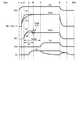
図5は、選択ワード線WL0にVcgv1を印加するときの波形図の第二例である。 FIG. 5 is a second example of a waveform diagram when Vcgv1 is applied to the selected word line WL0.
第二例では、選択ワード線WL0については、メモリセルアレイ内のA点及びB点の波形変化を比較して表し、非選択ワード線WL1については、メモリセルアレイ内のC点及びD点の波形変化を比較して表している。 In the second example, the selected word line WL0 is represented by comparing waveform changes at points A and B in the memory cell array, and the unselected word line WL1 is represented by waveform changes at points C and D in the memory cell array. Are shown in comparison.
B点及びD点の波形図は、時刻t2〜t5の範囲内においてA点及びC点の波形図と異なる。点線は、A点及びC点の波形図を表し、実線は、B点及びD点の波形図を表している。 The waveform diagrams at the points B and D are different from the waveform diagrams at the points A and C within the range of the times t2 to t5. A dotted line represents a waveform diagram at points A and C, and a solid line represents a waveform diagram at points B and D.
時刻t2において、非選択ワード線WL1〜WL(i−1)の一端に非選択読み出し電位Vreadが印加されると、最もワード線ドライバに近いC点では、非選択ワード線WL1〜WL(i−1)の電位は、急峻に立ち上がり、直ちにVreadに到達する。 When the non-selected read potential Vread is applied to one end of the non-selected word lines WL1 to WL (i-1) at time t2, the non-selected word lines WL1 to WL (i--) are applied at the point C closest to the word line driver. The potential of 1) rises sharply and immediately reaches Vread.
これに対し、最もワード線ドライバから遠いD点では、非選択ワード線WL1〜WL(i−1)の電位は、配線抵抗及び配線容量の影響により緩やかに立ち上がる。 On the other hand, at the point D farthest from the word line driver, the potentials of the unselected word lines WL1 to WL (i-1) rise gently due to the influence of the wiring resistance and the wiring capacitance.
時刻t3において、選択ワード線WL0の一端に選択読み出し電位Vcgv1が印加されると、A点では、選択ワード線WL0の電位は、直ちにVcgv1になるが、B点では、Vcgv1がA点からB点に伝わるまでに相当の時間を要するため、直ちにVcgv1になることはない。 At time t3, when the selected read potential Vcgv1 is applied to one end of the selected word line WL0, the potential of the selected word line WL0 immediately becomes Vcgv1 at point A, but at point B, Vcgv1 changes from point A to point B. Vcgv1 does not immediately occur because a considerable amount of time is required to be transmitted to.
一方で、非選択ワード線WL1のD点の電位は、配線抵抗及び配線容量の影響により緩やかに立ち上がるため、選択ワード線WL0のB点の電位は、選択ワード線WL0と非選択ワード線WL1との容量カップリングにより、Vread付近までオーバーシュートする。 On the other hand, since the potential at the point D of the unselected word line WL1 rises gently due to the influence of the wiring resistance and the wiring capacitance, the potential at the point B of the selected word line WL0 is the selected word line WL0 and the unselected word line WL1. Overshoot to near Vread due to the capacitive coupling.
従って、センスの開始は、誤読み出しを防止するため、B点の電位が、Vread付近からVcgv1に低下してからでないと行うことはできない。つまり、選択ワード線WL0にVcgv1を印加し始めてからセンス開始するまでのワード線セットアップ期間tw(fix)が必要になる。 Therefore, in order to prevent erroneous reading, the start of sensing can be performed only after the potential at point B has dropped from near Vread to Vcgv1. That is, a word line setup period tw (fix) is required from the start of applying Vcgv1 to the selected word line WL0 until the start of sensing.
ここで、B点の電位がVcgv1になる時点を安定点(Stable point)と称することにする。B点の電位がVcgv1になるとは、B点の電位がVcgv1±αの範囲内に収まることを意味するものとする。αの値は、例えば、Vcgv1の値の10%とする。仮にVcgv1を0.5Vとすると、αは、0.05Vとなる。 Here, the time when the potential at the point B becomes Vcgv1 is referred to as a stable point. The potential at point B being Vcgv1 means that the potential at point B falls within the range of Vcgv1 ± α. The value of α is, for example, 10% of the value of Vcgv1. If Vcgv1 is 0.5V, α is 0.05V.
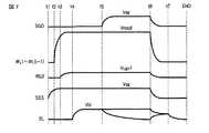
図6は、選択ワード線WL0にVcgv3を印加するときの波形図である。 FIG. 6 is a waveform diagram when Vcgv3 is applied to the selected word line WL0.
この波形図では、選択ワード線WL0については、メモリセルアレイ内のA点及びB点の波形変化を比較して表し、非選択ワード線WL1については、メモリセルアレイ内のC点及びD点の波形変化を比較して表している。 In this waveform diagram, the selected word line WL0 is represented by comparing waveform changes at points A and B in the memory cell array, and the unselected word line WL1 is represented by waveform changes at points C and D in the memory cell array. Are shown in comparison.
Vcgv1は、選択読み出し電位の最も低い値であるのに対し、Vcgv3は、選択読み出し電位の最も高い値である。 Vcgv1 is the lowest value of the selected read potential, while Vcgv3 is the highest value of the selected read potential.
この波形図から分かることは、選択読み出し電位の値が大きくなるに従い、安定点(Stable point)が時刻t3(選択ワード線の選択読み出し電位を印加し始める時点)に近づくことにある。 As can be seen from this waveform diagram, as the value of the selected read potential increases, the stable point (stable point) approaches time t3 (the time when the selected read potential of the selected word line starts to be applied).
しかし、従来においては、同図に示すように、ワード線セットアップ期間tw(fix)は、選択読み出し電位の値にかかわらず、選択読み出し電位がVcgv1のときの最も長い期間に固定される。 However, conventionally, as shown in the figure, the word line setup period tw (fix) is fixed to the longest period when the selected read potential is Vcgv1 regardless of the value of the selected read potential.
このようなことから、本発明では、選択読み出し電位の値に応じて、ワード線セットアップ期間を異ならせることを提案する。 For this reason, the present invention proposes to change the word line setup period in accordance with the value of the selected read potential.
即ち、選択読み出し電位の値が大きくなるに従い、ワード線セットアップ期間を短くする。例えば、選択読み出し電位がVcgv3のときのワード線セットアップ期間をtw’とすれば、時刻t5を、時刻t5’に早めることができ、読み出し動作の高速化に貢献できる。 That is, the word line setup period is shortened as the value of the selected read potential increases. For example, if the word line setup period when the selected read potential is Vcgv3 is tw ', the time t5 can be advanced to the time t5', which can contribute to the speeding up of the read operation.
以上、本発明の原理について説明したが、同様のことは、以下の読み出し波形についても言える。 Although the principle of the present invention has been described above, the same can be said for the following readout waveforms.
図7は、選択ワード線WL0にVcgv1を印加するときの波形図の第三例である。 FIG. 7 is a third example of a waveform diagram when Vcgv1 is applied to the selected word line WL0.
第三例では、選択ワード線WL0については、メモリセルアレイ内のA点の波形変化を表し、非選択ワード線WL1については、メモリセルアレイ内のC点の波形変化を表している。 In the third example, the selected word line WL0 represents a waveform change at point A in the memory cell array, and the non-selected word line WL1 represents a waveform change at point C in the memory cell array.
この波形図の特徴は、図4の波形図と比べると、ソース線側セレクトゲートトランジスタのゲート電位(セレクトゲート線SGSの電位)を立ち上げるタイミングと、ビット線側セレクトゲートトランジスタのゲート電位(セレクトゲート線SGDの電位)を立ち上げるタイミングとが、逆になっていることにある。 Compared with the waveform diagram of FIG. 4, this waveform diagram is characterized in that the gate potential of the source line side select gate transistor (potential of the select gate line SGS) rises and the gate potential of the bit line side select gate transistor (select). The timing at which the potential of the gate line SGD is raised is reversed.
即ち、時刻t1において、ソース線側セレクトゲートトランジスタのゲート電位(セレクトゲート線SGSの電位)は、Vsgに上昇し始め、時刻t5において、ビット線側セレクトゲートトランジスタのゲート電位(セレクトゲート線SGDの電位)は、Vsgに上昇し始める。 That is, at time t1, the gate potential of the source line side select gate transistor (the potential of the select gate line SGS) starts to rise to Vsg, and at time t5, the gate potential of the bit line side select gate transistor (of the select gate line SGD). Potential) starts to rise to Vsg.
その他の点は、図4の波形図と同じである。 The other points are the same as the waveform diagram of FIG.
ここで、図4の波形図と図7の波形図とを組み合わせることも可能である。 Here, the waveform diagram of FIG. 4 and the waveform diagram of FIG. 7 can be combined.
例えば、WL0を選択ワード線とするときに、図7の波形図を採用し、WL1〜WL(i−1)のうちの1本を選択ワード線とするときに、図4の波形図を採用してもよい。 For example, when WL0 is a selected word line, the waveform diagram of FIG. 7 is adopted, and when one of WL1 to WL (i−1) is a selected word line, the waveform diagram of FIG. 4 is adopted. May be.
また、WL0〜WL(i−1)のソース線側半分の複数のワード線のうちの1本を選択ワード線とするときに、図7の波形図を採用し、WL0〜WL(i−1)のビット線側半分の複数のワード線のうちの1本を選択ワード線とするときに、図4の波形図を採用してもよい。 Further, when one of the plurality of word lines on the source line side half of WL0 to WL (i−1) is used as the selected word line, the waveform diagram of FIG. 7 is adopted, and WL0 to WL (i−1). 4) may be employed when one of the plurality of word lines on the bit line side half is used as the selected word line.
図8は、選択ワード線WL0にVcgv1を印加するときの波形図の第四例である。 FIG. 8 is a fourth example of a waveform diagram when Vcgv1 is applied to the selected word line WL0.
第四例では、選択ワード線WL0については、メモリセルアレイ内のA点の波形変化を表し、非選択ワード線WL1については、メモリセルアレイ内のC点の波形変化を表している。 In the fourth example, the selected word line WL0 represents a waveform change at point A in the memory cell array, and the non-selected word line WL1 represents a waveform change at point C in the memory cell array.
この波形図の特徴は、図4の波形図と比べると、非選択ワード線WL1〜WL(i−1)の電位を、複数ステップ(例えば、二ステップ)で、非選択読み出し電位Vreadまで立ち上げることにある。 Compared with the waveform diagram of FIG. 4, this waveform diagram is characterized by raising the potential of the unselected word lines WL1 to WL (i−1) to the unselected read potential Vread in a plurality of steps (for example, two steps). There is.
即ち、時刻t0において、ビット線側セレクトゲートトランジスタのゲート電位(セレクトゲート線SGDの電位)は、Vsgに上昇し始める。また、時刻t1において、非選択ワード線WL1〜WL(i−1)の電位は、接地電位Vssから中間電位Vmに上昇し始め、さらに、時刻t2において、非選択ワード線WL1〜WL(i−1)の電位は、中間電位Vmから非選択読み出し電位Vreadに上昇し始める。 That is, at time t0, the gate potential of the bit line side select gate transistor (the potential of the select gate line SGD) starts to rise to Vsg. Further, at time t1, the potentials of the unselected word lines WL1 to WL (i-1) start to rise from the ground potential Vss to the intermediate potential Vm, and at time t2, the unselected word lines WL1 to WL (i−). The potential of 1) starts to rise from the intermediate potential Vm to the non-selected read potential Vread.
その他の点は、図4の波形図と同じである。 The other points are the same as the waveform diagram of FIG.
図9は、センスアンプの例を示している。 FIG. 9 shows an example of the sense amplifier.
センスアンプSAは、ABL(All Bit Line)センシング方式に適用される。 The sense amplifier SA is applied to an ABL (All Bit Line) sensing method.
NANDセルユニット21は、クランプ回路31を介してセンスアンプSAに接続される。クランプ回路31は、ゲートに制御信号BLCが入力されるNチャネルMOSトランジスタから構成される。 The
センスアンプSAは、電圧クランプ回路32、プリチャージ回路33、ディスクリミネート回路(discriminator)34及びラッチ回路35から構成される。 The sense amplifier SA includes a
電圧クランプ回路32は、電源端子Vddとビット線BLとの間に直列接続されるNチャネルMOSトランジスタ36,37から構成される。MOSトランジスタ36のゲートは、ラッチ回路35の出力端子に接続され、MOSトランジスタ37のゲートには、制御信号BLXが入力される。 The
プリチャージ回路33は、ゲートに制御信号FLTが入力されるPチャネルMOSトランジスタ38から構成される。プリチャージ回路33は、センスノードSENをプリチャージする。
ディスクリミネート回路34は、キャパシタ39、PチャネルMOSトランジスタ40,41及びNチャネルMOSトランジスタ42から構成される。MOSトランジスタ40のゲートには、制御信号STBが入力され、MOSトランジスタ42のゲートには、制御信号RSTが入力される。 The
MOSトランジスタ41のゲートは、センスノードSENに接続される。 The gate of
ラッチ回路35は、PチャネルMOSトランジスタ43,44,47及びNチャネルMOSトランジスタ45,46,48とから構成される。MOSトランジスタ43,44,45,46は、フリップフロップ接続された二つのインバータを構成する。MOSトランジスタ47のゲートには、制御信号RSTが入力され、MOSトランジスタ48のゲートには、制御信号STBが入力される。 The
図10は、選択ワード線WL0にVcgv1を印加するときの波形図の第五例である。 FIG. 10 is a fifth example of a waveform diagram when Vcgv1 is applied to the selected word line WL0.
第五例では、図9のセンスアンプを用いたABLセンシング方式を採用する。 In the fifth example, an ABL sensing method using the sense amplifier of FIG. 9 is adopted.
選択ワード線WL0については、メモリセルアレイ内のA点の波形変化を表し、非選択ワード線WL1については、メモリセルアレイ内のC点の波形変化を表している。 The selected word line WL0 represents a waveform change at point A in the memory cell array, and the non-selected word line WL1 represents a waveform change at point C in the memory cell array.
まず、時刻t1において、ソース線側セレクトゲートトランジスタのゲート電位(セレクトゲート線SGSの電位)及びビット線側セレクトゲートトランジスタのゲート電位(セレクトゲート線SGDの電位)は、Vsgに上昇し始める。 First, at time t1, the gate potential of the source line side select gate transistor (the potential of the select gate line SGS) and the gate potential of the bit line side select gate transistor (the potential of the select gate line SGD) start to rise to Vsg.
この後、時刻t2において、非選択ワード線WL1〜WL(i−1)の電位は、Vreadに上昇し始め、時刻t3において、選択ワード線WL0の電位は、Vcgv1に上昇し始める。 Thereafter, at time t2, the potentials of the unselected word lines WL1 to WL (i−1) begin to rise to Vread, and at time t3, the potential of the selected word line WL0 begins to rise to Vcgv1.
また、時刻t4において、センスノードSENを充電し始める。即ち、図9の制御信号FLTを“L”にし、センスノードSENを、Vsenに充電する。 At time t4, the sense node SEN starts to be charged. That is, the control signal FLT in FIG. 9 is set to “L”, and the sense node SEN is charged to Vsen.
そして、時刻t5において、制御信号FLTを“H”にすると共に、制御信号STBを“H”にし、制御信号RSTを“L”にする。 At time t5, the control signal FLT is set to “H”, the control signal STB is set to “H”, and the control signal RST is set to “L”.
この時、選択メモリセルの閾値が選択読み出し電位Vcgv1よりも低いと、図9のNANDセルユニット21内の選択メモリセルは、オン状態になる。 At this time, if the threshold value of the selected memory cell is lower than the selected read potential Vcgv1, the selected memory cell in the
このため、センスノードSENは、放電され、図9のMOSトランジスタ41がオン状態になる。即ち、ラッチ回路35には、“H”がラッチされ、NチャネルMOSトランジスタ49によりビット線BLが放電される。 Therefore, the sense node SEN is discharged, and the
また、選択メモリセルの閾値が選択読み出し電位Vcgv1よりも高いと、図9のNANDセルユニット21内の選択メモリセルは、オフ状態になる。 When the threshold value of the selected memory cell is higher than the selected read potential Vcgv1, the selected memory cell in the
このため、センスノードSENは、Vsenを維持し、図9のMOSトランジスタ41は、オフ状態を維持する。即ち、ラッチ回路35には、“L”がラッチされる。 For this reason, the sense node SEN maintains Vsen, and the
最後に、時刻t6において、制御信号FLTを“L”にし、ソース線側セレクトゲートトランジスタのゲート電位(セレクトゲート線SGSの電位)を立ち下げる。 Finally, at time t6, the control signal FLT is set to “L”, and the gate potential of the source line side select gate transistor (the potential of the select gate line SGS) is lowered.
また、時刻t7において、全てのワード線WL0〜WL(i−1)及びビット線側セレクトゲートトランジスタのゲート電位(セレクトゲート線SGDの電位)を立ち下げ、接地電位Vssにする。 At time t7, the gate potentials of all the word lines WL0 to WL (i−1) and the bit line side select gate transistors (the potential of the select gate line SGD) are lowered to the ground potential Vss.
図11は、選択ワード線WL0にVcgv1を印加するときの波形図の第六例である。 FIG. 11 is a sixth example of a waveform diagram when Vcgv1 is applied to the selected word line WL0.
第六例では、図9のセンスアンプを用いたABLセンシング方式を採用する。 In the sixth example, an ABL sensing method using the sense amplifier of FIG. 9 is adopted.
第六例では、選択ワード線WL0については、メモリセルアレイ内のA点及びB点の波形変化を比較して表し、非選択ワード線WL1については、メモリセルアレイ内のC点及びD点の波形変化を比較して表している。 In the sixth example, the selected word line WL0 is represented by comparing waveform changes at points A and B in the memory cell array, and the unselected word line WL1 is represented by waveform changes at points C and D in the memory cell array. Are shown in comparison.
B点及びD点の波形図は、時刻t2〜t5の範囲内においてA点及びC点の波形図と異なる。点線は、A点及びC点の波形図を表し、実線は、B点及びD点の波形図を表している。 The waveform diagrams at the points B and D are different from the waveform diagrams at the points A and C within the range of the times t2 to t5. A dotted line represents a waveform diagram at points A and C, and a solid line represents a waveform diagram at points B and D.
時刻t2において、非選択ワード線WL1〜WL(i−1)の一端に非選択読み出し電位Vreadが印加されると、最もワード線ドライバに近いC点では、非選択ワード線WL1〜WL(i−1)の電位は、急峻に立ち上がり、直ちにVreadに到達する。 When the non-selected read potential Vread is applied to one end of the non-selected word lines WL1 to WL (i-1) at time t2, the non-selected word lines WL1 to WL (i--) are applied at the point C closest to the word line driver. The potential of 1) rises sharply and immediately reaches Vread.
これに対し、最もワード線ドライバから遠いD点では、非選択ワード線WL1〜WL(i−1)の電位は、配線抵抗及び配線容量の影響により緩やかに立ち上がる。 On the other hand, at the point D farthest from the word line driver, the potentials of the unselected word lines WL1 to WL (i-1) rise gently due to the influence of the wiring resistance and the wiring capacitance.
時刻t3において、選択ワード線WL0の一端に選択読み出し電位Vcgv1が印加されると、A点では、選択ワード線WL0の電位は、直ちにVcgv1になるが、B点では、Vcgv1がA点からB点に伝わるまでに相当の時間を要するため、直ちにVcgv1になることはない。 At time t3, when the selected read potential Vcgv1 is applied to one end of the selected word line WL0, the potential of the selected word line WL0 immediately becomes Vcgv1 at point A, but at point B, Vcgv1 changes from point A to point B. Vcgv1 does not immediately occur because a considerable amount of time is required to be transmitted to.
一方で、非選択ワード線WL1のD点の電位は、配線抵抗及び配線容量の影響により緩やかに立ち上がるため、選択ワード線WL0のB点の電位は、選択ワード線WL0と非選択ワード線WL1との容量カップリングにより、Vread付近までオーバーシュートする。 On the other hand, since the potential at the point D of the unselected word line WL1 rises gently due to the influence of the wiring resistance and the wiring capacitance, the potential at the point B of the selected word line WL0 is the selected word line WL0 and the unselected word line WL1. Overshoot to near Vread due to the capacitive coupling.
従って、センスの開始は、誤読み出しを防止するため、B点の電位が、Vread付近からVcgv1に低下してからでないと行うことはできない。つまり、選択ワード線WL0にVcgv1を印加し始めてからセンス開始するまでのワード線セットアップ期間tw(fix)が必要になる。 Therefore, in order to prevent erroneous reading, the start of sensing can be performed only after the potential at point B has dropped from near Vread to Vcgv1. That is, a word line setup period tw (fix) is required from the start of applying Vcgv1 to the selected word line WL0 until the start of sensing.
ここで、B点の電位がVcgv1になる時点は、上述のように、安定点(Stable point)と称される。B点の電位がVcgv1になるとは、B点の電位がVcgv1±αの範囲内に収まることを意味するものとする。αの値は、例えば、Vcgv1の値の10%とする。仮にVcgv1を0.5Vとすると、αは、0.05Vとなる。 Here, the point in time when the potential at the point B becomes Vcgv1 is referred to as a stable point as described above. The potential at point B being Vcgv1 means that the potential at point B falls within the range of Vcgv1 ± α. The value of α is, for example, 10% of the value of Vcgv1. If Vcgv1 is 0.5V, α is 0.05V.
図12は、選択ワード線WL0にVcgv3を印加するときの波形図である。 FIG. 12 is a waveform diagram when Vcgv3 is applied to the selected word line WL0.
この波形図は、図9のセンスアンプを用いたABLセンシング方式に関する。 This waveform diagram relates to an ABL sensing method using the sense amplifier of FIG.
この波形図では、選択ワード線WL0については、メモリセルアレイ内のA点及びB点の波形変化を比較して表し、非選択ワード線WL1については、メモリセルアレイ内のC点及びD点の波形変化を比較して表している。 In this waveform diagram, the selected word line WL0 is represented by comparing waveform changes at points A and B in the memory cell array, and the unselected word line WL1 is represented by waveform changes at points C and D in the memory cell array. Are shown in comparison.
Vcgv1は、選択読み出し電位の最も低い値であるのに対し、Vcgv3は、選択読み出し電位の最も高い値である。 Vcgv1 is the lowest value of the selected read potential, while Vcgv3 is the highest value of the selected read potential.
この波形図から分かることは、選択読み出し電位の値が大きくなるに従い、安定点(Stable point)が時刻t3(選択ワード線の選択読み出し電位を印加し始める時点)に近づくことにある。 As can be seen from this waveform diagram, as the value of the selected read potential increases, the stable point (stable point) approaches time t3 (the time when the selected read potential of the selected word line starts to be applied).
しかし、上述のように、従来においては、ワード線セットアップ期間tw(fix)は、選択読み出し電位の値にかかわらず、選択読み出し電位がVcgv1のときの最も長い期間に固定される。 However, as described above, conventionally, the word line setup period tw (fix) is fixed to the longest period when the selected read potential is Vcgv1 regardless of the value of the selected read potential.
このようなことから、本発明では、ABLセンシング方式においても、選択読み出し電位の値に応じて、ワード線セットアップ期間を異ならせることを提案する。 For this reason, the present invention proposes to change the word line setup period in accordance with the value of the selected read potential even in the ABL sensing method.
即ち、選択読み出し電位の値が大きくなるに従い、ワード線セットアップ期間を短くする。例えば、選択読み出し電位がVcgv3のときのワード線セットアップ期間をtw’とすれば、時刻t5を、時刻t5’に早めることができ、読み出し動作の高速化に貢献できる。 That is, the word line setup period is shortened as the value of the selected read potential increases. For example, if the word line setup period when the selected read potential is Vcgv3 is tw ', the time t5 can be advanced to the time t5', which can contribute to the speeding up of the read operation.
4. 実施例
(1) 第一実施例
第一実施例は、通常読み出し動作に関する。4). Example
(1) First example
The first embodiment relates to a normal read operation.
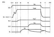
図13は、選択ワード線の読み出し電位とセットアップ期間との関係を示している。 FIG. 13 shows the relationship between the read potential of the selected word line and the setup period.
一つのメモリセルは、n(nは、三以上の自然数)値を記憶するものとする。 One memory cell stores n (n is a natural number of 3 or more) values.
この場合、選択読み出し電位Vcgrの数は、(n−1)個となる。これを、Vcgr1,Vcgr2,Vcgr3,…Vcgr(n−1)とする。但し、Vcgr1<Vcgr2<Vcgr3<…Vcgr(n−1)である。 In this case, the number of selected read potentials Vcgr is (n−1). This is Vcgr1, Vcgr2, Vcgr3,... Vcgr (n-1). However, Vcgr1 <Vcgr2 <Vcgr3 <... Vcgr (n-1).
また、選択読み出し電位Vcgr1,Vcgr2,Vcgr3,…Vcgr(n−1)に対応するワード線セットアップ期間を、tw1,tw2,tw3,…tw(n−1)とする。本発明の例によれば、tw1>tw2>tw3>…tw(n−1)となる。 Also, the word line setup period corresponding to the selected read potentials Vcgr1, Vcgr2, Vcgr3,... Vcgr (n−1) is tw1, tw2, tw3,. According to the example of the present invention, tw1> tw2> tw3>... Tw (n−1).
図14は、選択読み出し電位の値が大きくなるに従い、ワード線セットアップ期間が短くなる様子を示している。 FIG. 14 shows how the word line setup period is shortened as the value of the selected read potential increases.
この波形図内の時刻t2〜t5は、図4〜図7及び図10〜図12の波形図内の時刻t2〜t5に対応する。 Times t2 to t5 in this waveform diagram correspond to times t2 to t5 in the waveform diagrams of FIGS. 4 to 7 and FIGS.
例えば、選択読み出し電位が最も低い値Vcgr1のときのワード線セットアップ期間tw1を基準にすると、選択読み出し電位の値が1レベル上になるごとに、ワード線セットアップ期間は、約1μsec短縮される。 For example, with reference to the word line setup period tw1 when the selected read potential is the lowest value Vcgr1, the word line setup period is shortened by about 1 μsec each time the value of the selected read potential increases by one level.
従って、本発明の例は、多値化が進むほど(一つのメモリセルに記憶させるデータ数が増加するほど)、効果が顕著に表れる。 Therefore, the effect of the example of the present invention becomes more remarkable as the multi-value processing proceeds (as the number of data stored in one memory cell increases).
このように、選択読み出し電位Vcgrの値に応じて、ワード線セットアップ期間twを異ならせることにより、読み出し動作の高速化に貢献できる。 In this way, by varying the word line setup period tw according to the value of the selected read potential Vcgr, it is possible to contribute to speeding up the read operation.
(2) 第二実施例
第二実施例は、ベリファイ読み出し動作に関する。(2) Second embodiment
The second embodiment relates to a verify read operation.
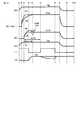
図15は、選択ワード線の読み出し電位とセットアップ期間との関係を示している。 FIG. 15 shows the relationship between the read potential of the selected word line and the setup period.
一つのメモリセルは、n(nは、三以上の自然数)値を記憶するものとする。 One memory cell stores n (n is a natural number of 3 or more) values.
この場合、選択読み出し電位Vcgvの数は、(n−1)個となる。これを、Vcgv1,Vcgv2,Vcgv3,…Vcgv(n−1)とする。但し、Vcgv1<Vcgv2<Vcgv3<…Vcgv(n−1)である。 In this case, the number of selected read potentials Vcgv is (n−1). This is Vcgv1, Vcgv2, Vcgv3,... Vcgv (n−1). However, Vcgv1 <Vcgv2 <Vcgv3 <... Vcgv (n−1).
また、選択読み出し電位Vcgv1,Vcgv2,Vcgv3,…Vcgv(n−1)に対応するワード線セットアップ期間を、tw1,tw2,tw3,…tw(n−1)とする。本発明の例によれば、tw1>tw2>tw3>…tw(n−1)となる。 Also, the word line setup period corresponding to the selected read potentials Vcgv1, Vcgv2, Vcgv3,... Vcgv (n−1) is tw1, tw2, tw3,. According to the example of the present invention, tw1> tw2> tw3>... Tw (n−1).
図16は、選択読み出し電位の値が大きくなるに従い、ワード線セットアップ期間が短くなる様子を示している。 FIG. 16 shows how the word line setup period is shortened as the value of the selected read potential increases.
この波形図内の時刻t2〜t5は、図4〜図7及び図10〜図12の波形図内の時刻t2〜t5に対応する。 Times t2 to t5 in this waveform diagram correspond to times t2 to t5 in the waveform diagrams of FIGS. 4 to 7 and FIGS.
例えば、選択読み出し電位が最も低い値Vcgv1のときのワード線セットアップ期間tw1を基準にすると、選択読み出し電位の値が1レベル上になるごとに、ワード線セットアップ期間は、約1μsec短縮される。 For example, with reference to the word line setup period tw1 when the selected read potential is the lowest value Vcgv1, the word line setup period is shortened by about 1 μsec each time the value of the selected read potential increases by one level.
従って、本発明の例は、多値化が進むほど(一つのメモリセルに記憶させるデータ数が増加するほど)、効果が顕著に表れる。 Therefore, the effect of the example of the present invention becomes more remarkable as the multi-value processing proceeds (as the number of data stored in one memory cell increases).
また、多値化が進むほど、ベリファイ回数が多くなる傾向にあるため、本発明の例は、このようなベリファイ回数の増大に対しても非常に有効である。 Moreover, since the number of verifications tends to increase as the number of values increases, the example of the present invention is very effective for such an increase in the number of verifications.
このように、選択読み出し電位Vcgvの値に応じて、ワード線セットアップ期間twを異ならせることにより、読み出し動作の高速化に貢献できる。 In this way, by varying the word line setup period tw according to the value of the selected read potential Vcgv, it is possible to contribute to speeding up the read operation.
5. 適用例
本発明の例は、多値NANDフラッシュメモリに有効である。また、本発明の例は、一つのメモリセルが三値以上を記憶する多値不揮発性半導体メモリ全般に適用可能である。5). Application examples
The example of the present invention is effective for a multi-level NAND flash memory. Further, the example of the present invention can be applied to all multi-value nonvolatile semiconductor memories in which one memory cell stores three or more values.
6. むすび
本発明によれば、ワード線セットアップ期間の設定を工夫することにより読み出し動作を高速化できる。6). Conclusion
According to the present invention, the read operation can be speeded up by devising the setting of the word line setup period.
本発明の例は、上述の実施形態に限定されるものではなく、その要旨を逸脱しない範囲で、各構成要素を変形して具体化できる。また、上述の実施形態に開示されている複数の構成要素の適宜な組み合せにより種々の発明を構成できる。例えば、上述の実施形態に開示される全構成要素から幾つかの構成要素を削除してもよいし、異なる実施形態の構成要素を適宜組み合わせてもよい。 The example of the present invention is not limited to the above-described embodiment, and can be embodied by modifying each component without departing from the gist thereof. Various inventions can be configured by appropriately combining a plurality of constituent elements disclosed in the above-described embodiments. For example, some constituent elements may be deleted from all the constituent elements disclosed in the above-described embodiments, or constituent elements of different embodiments may be appropriately combined.
11: メモリセルアレイ、 12: データ回路、 13: I/Oバッファ、 14: アドレスバッファ、 15: ロウデコーダ、 16: ワード線ドライバ、 17: カラムデコーダ、 18: ベリファイ回路、 19: 電位発生回路、 20: 制御回路、 21: NANDセルユニット。 11: Memory cell array, 12: Data circuit, 13: I / O buffer, 14: Address buffer, 15: Row decoder, 16: Word line driver, 17: Column decoder, 18: Verify circuit, 19: Potential generation circuit, 20 : Control circuit, 21: NAND cell unit.
Claims (5)
Translated fromJapanesePriority Applications (2)
| Application Number | Priority Date | Filing Date | Title |
|---|---|---|---|
| JP2008302758AJP2010129125A (en) | 2008-11-27 | 2008-11-27 | Multivalue nonvolatile semiconductor memory |
| US12/563,274US7995389B2 (en) | 2008-11-27 | 2009-09-21 | Multi-level nonvolatile semiconductor memory |
Applications Claiming Priority (1)
| Application Number | Priority Date | Filing Date | Title |
|---|---|---|---|
| JP2008302758AJP2010129125A (en) | 2008-11-27 | 2008-11-27 | Multivalue nonvolatile semiconductor memory |
Publications (1)
| Publication Number | Publication Date |
|---|---|
| JP2010129125Atrue JP2010129125A (en) | 2010-06-10 |
Family
ID=42196111
Family Applications (1)
| Application Number | Title | Priority Date | Filing Date |
|---|---|---|---|
| JP2008302758APendingJP2010129125A (en) | 2008-11-27 | 2008-11-27 | Multivalue nonvolatile semiconductor memory |
Country Status (2)
| Country | Link |
|---|---|
| US (1) | US7995389B2 (en) |
| JP (1) | JP2010129125A (en) |
Cited By (4)
| Publication number | Priority date | Publication date | Assignee | Title |
|---|---|---|---|---|
| JP2010140554A (en)* | 2008-12-11 | 2010-06-24 | Samsung Electronics Co Ltd | Method of reading nonvolatile semiconductor memory device |
| JP2017216025A (en)* | 2016-05-31 | 2017-12-07 | 東芝メモリ株式会社 | Semiconductor memory device |
| WO2020105596A1 (en)* | 2018-11-20 | 2020-05-28 | 国立大学法人静岡大学 | Drive circuit and electronic device |
| JP2022525116A (en)* | 2019-11-28 | 2022-05-11 | 長江存儲科技有限責任公司 | How to speed up reading data from memory devices |
Families Citing this family (3)
| Publication number | Priority date | Publication date | Assignee | Title |
|---|---|---|---|---|
| CN103594116A (en)* | 2012-08-15 | 2014-02-19 | 群联电子股份有限公司 | Data reading method, control circuit, memory module and memory storage device |
| TWI490865B (en)* | 2012-08-15 | 2015-07-01 | Phison Electronics Corp | Data reading method, memory controller and memory storage apparatus |
| KR102116671B1 (en) | 2014-07-30 | 2020-06-01 | 삼성전자주식회사 | Nonvolatile memory device and wordline driving method thereof |
Citations (12)
| Publication number | Priority date | Publication date | Assignee | Title |
|---|---|---|---|---|
| JPH05225792A (en)* | 1991-09-27 | 1993-09-03 | Hyundai Electron Ind Co Ltd | Sensing apparatus of memory device provided with nand-type cell |
| JPH10208490A (en)* | 1997-01-21 | 1998-08-07 | Samsung Electron Co Ltd | Nonvolatile semiconductor memory device |
| JP2000091546A (en)* | 1998-09-11 | 2000-03-31 | Toshiba Corp | Non-volatile semiconductor memory |
| JP2002133885A (en)* | 2000-10-30 | 2002-05-10 | Toshiba Corp | Nonvolatile semiconductor memory device |
| JP2004326866A (en)* | 2003-04-22 | 2004-11-18 | Toshiba Corp | Nonvolatile semiconductor memory device and electronic device using the same |
| JP2005285185A (en)* | 2004-03-29 | 2005-10-13 | Toshiba Corp | Semiconductor memory device |
| JP2006107577A (en)* | 2004-10-01 | 2006-04-20 | Toshiba Corp | Semiconductor memory device and memory card |
| JP2007048410A (en)* | 2005-08-12 | 2007-02-22 | Toshiba Corp | Semiconductor memory device |
| JP2007133999A (en)* | 2005-11-11 | 2007-05-31 | Toshiba Corp | Nonvolatile semiconductor memory device and memory card equipped with the same |
| JP2007157289A (en)* | 2005-12-07 | 2007-06-21 | Toshiba Corp | Nonvolatile semiconductor device |
| WO2007078611A1 (en)* | 2005-12-16 | 2007-07-12 | Sandisk Corporation | Reading non-volatile storage with efficient control of non-selected word lines |
| JP2008052808A (en)* | 2006-08-24 | 2008-03-06 | Toshiba Corp | Nonvolatile semiconductor memory device, data reading method thereof, and memory card |
Family Cites Families (6)
| Publication number | Priority date | Publication date | Assignee | Title |
|---|---|---|---|---|
| KR100323554B1 (en) | 1997-05-14 | 2002-03-08 | 니시무로 타이죠 | Non-volatile semiconductor memory |
| US7196931B2 (en) | 2002-09-24 | 2007-03-27 | Sandisk Corporation | Non-volatile memory and method with reduced source line bias errors |
| KR100512181B1 (en) | 2003-07-11 | 2005-09-05 | 삼성전자주식회사 | Flash memory device having multi-level cell and method for its reading operation and program operation |
| KR100795634B1 (en)* | 2005-11-11 | 2008-01-17 | 가부시끼가이샤 도시바 | Nonvolatile semiconductor memory device, data reading method and memory card |
| US7369437B2 (en) | 2005-12-16 | 2008-05-06 | Sandisk Corporation | System for reading non-volatile storage with efficient setup |
| JP4510060B2 (en)* | 2007-09-14 | 2010-07-21 | 株式会社東芝 | Read / write control method for nonvolatile semiconductor memory device |
- 2008
- 2008-11-27JPJP2008302758Apatent/JP2010129125A/enactivePending
- 2009
- 2009-09-21USUS12/563,274patent/US7995389B2/enactiveActive
Patent Citations (13)
| Publication number | Priority date | Publication date | Assignee | Title |
|---|---|---|---|---|
| JPH05225792A (en)* | 1991-09-27 | 1993-09-03 | Hyundai Electron Ind Co Ltd | Sensing apparatus of memory device provided with nand-type cell |
| JPH10208490A (en)* | 1997-01-21 | 1998-08-07 | Samsung Electron Co Ltd | Nonvolatile semiconductor memory device |
| JP2000091546A (en)* | 1998-09-11 | 2000-03-31 | Toshiba Corp | Non-volatile semiconductor memory |
| JP2002133885A (en)* | 2000-10-30 | 2002-05-10 | Toshiba Corp | Nonvolatile semiconductor memory device |
| JP2004326866A (en)* | 2003-04-22 | 2004-11-18 | Toshiba Corp | Nonvolatile semiconductor memory device and electronic device using the same |
| JP2005285185A (en)* | 2004-03-29 | 2005-10-13 | Toshiba Corp | Semiconductor memory device |
| JP2006107577A (en)* | 2004-10-01 | 2006-04-20 | Toshiba Corp | Semiconductor memory device and memory card |
| JP2007048410A (en)* | 2005-08-12 | 2007-02-22 | Toshiba Corp | Semiconductor memory device |
| JP2007133999A (en)* | 2005-11-11 | 2007-05-31 | Toshiba Corp | Nonvolatile semiconductor memory device and memory card equipped with the same |
| JP2007157289A (en)* | 2005-12-07 | 2007-06-21 | Toshiba Corp | Nonvolatile semiconductor device |
| WO2007078611A1 (en)* | 2005-12-16 | 2007-07-12 | Sandisk Corporation | Reading non-volatile storage with efficient control of non-selected word lines |
| JP2009520310A (en)* | 2005-12-16 | 2009-05-21 | サンディスク コーポレイション | Method for reading non-volatile memory by effectively controlling non-selected word lines |
| JP2008052808A (en)* | 2006-08-24 | 2008-03-06 | Toshiba Corp | Nonvolatile semiconductor memory device, data reading method thereof, and memory card |
Cited By (6)
| Publication number | Priority date | Publication date | Assignee | Title |
|---|---|---|---|---|
| JP2010140554A (en)* | 2008-12-11 | 2010-06-24 | Samsung Electronics Co Ltd | Method of reading nonvolatile semiconductor memory device |
| JP2017216025A (en)* | 2016-05-31 | 2017-12-07 | 東芝メモリ株式会社 | Semiconductor memory device |
| WO2020105596A1 (en)* | 2018-11-20 | 2020-05-28 | 国立大学法人静岡大学 | Drive circuit and electronic device |
| US11735264B2 (en) | 2018-11-20 | 2023-08-22 | National University Corporation Shizuoka University | Drive circuit and electronic device |
| JP2022525116A (en)* | 2019-11-28 | 2022-05-11 | 長江存儲科技有限責任公司 | How to speed up reading data from memory devices |
| JP7358496B2 (en) | 2019-11-28 | 2023-10-10 | 長江存儲科技有限責任公司 | How to increase the speed of reading data from memory devices |
Also Published As
| Publication number | Publication date |
|---|---|
| US20100128526A1 (en) | 2010-05-27 |
| US7995389B2 (en) | 2011-08-09 |
Similar Documents
| Publication | Publication Date | Title |
|---|---|---|
| JP5193830B2 (en) | Nonvolatile semiconductor memory | |
| JP4856138B2 (en) | Nonvolatile semiconductor memory device | |
| CN102314941B (en) | The method of nonvolatile semiconductor memory member, storage system and execution read operation | |
| JP4791806B2 (en) | Semiconductor memory device and data writing method thereof | |
| KR101119343B1 (en) | Program method of semiconductor memory device | |
| KR101099835B1 (en) | Semiconductor memory device and operation method thereof | |
| JP5992983B2 (en) | Nonvolatile semiconductor memory device | |
| CN103177760B (en) | Semiconductor storage unit and its operating method | |
| KR20130069526A (en) | Non-volatile memory device | |
| JP2009043390A (en) | Soft program method in non-volatile memory device | |
| JP4342383B2 (en) | Semiconductor memory device | |
| KR20130072518A (en) | Semiconductor device and operating method thereof | |
| JP2010129125A (en) | Multivalue nonvolatile semiconductor memory | |
| TWI559320B (en) | Semiconductor storage device | |
| US20150078097A1 (en) | Semiconductor memory apparatus and method for erasing the same | |
| US20180068738A1 (en) | Semiconductor memory device | |
| JP4698605B2 (en) | Semiconductor device and method for controlling semiconductor device | |
| JP3961759B2 (en) | Nonvolatile semiconductor memory device | |
| CN114446359A (en) | Nonvolatile memory device that performs precharging on cell strings and programming method thereof | |
| CN118053466A (en) | Semiconductor device, method of operating the same, and method of operating controller | |
| KR101201888B1 (en) | Program method of semiconductor device | |
| JP5081755B2 (en) | Nonvolatile semiconductor memory device and reading method thereof | |
| JP4794231B2 (en) | Nonvolatile semiconductor memory device | |
| KR101610176B1 (en) | Semiconductor memory apparatus and method for erasing the same | |
| CN118230792A (en) | Memory device and operation method thereof |
Legal Events
| Date | Code | Title | Description |
|---|---|---|---|
| A621 | Written request for application examination | Free format text:JAPANESE INTERMEDIATE CODE: A621 Effective date:20110302 | |
| A977 | Report on retrieval | Free format text:JAPANESE INTERMEDIATE CODE: A971007 Effective date:20120725 | |
| A131 | Notification of reasons for refusal | Free format text:JAPANESE INTERMEDIATE CODE: A131 Effective date:20120821 | |
| A02 | Decision of refusal | Free format text:JAPANESE INTERMEDIATE CODE: A02 Effective date:20121218 |