JP2010128259A - Absorption type multilayer film nd filter and method of manufacturing the same - Google Patents
Absorption type multilayer film nd filter and method of manufacturing the sameDownload PDFInfo
- Publication number
- JP2010128259A JP2010128259AJP2008303845AJP2008303845AJP2010128259AJP 2010128259 AJP2010128259 AJP 2010128259AJP 2008303845 AJP2008303845 AJP 2008303845AJP 2008303845 AJP2008303845 AJP 2008303845AJP 2010128259 AJP2010128259 AJP 2010128259A
- Authority
- JP
- Japan
- Prior art keywords
- film
- roll
- absorption
- film layer
- filter
- Prior art date
- Legal status (The legal status is an assumption and is not a legal conclusion. Google has not performed a legal analysis and makes no representation as to the accuracy of the status listed.)
- Pending
Links
Images


Landscapes
- Optical Elements Other Than Lenses (AREA)
- Laminated Bodies (AREA)
Abstract
Translated fromJapaneseDescription
Translated fromJapanese本発明は、400〜700nmの透過光を減衰させる吸収型多層膜NDフィルターの製造方法に係り、特に光軸中心から離れるにつれて透過率が徐々に低くなるグラデーション濃度分布を有する吸収型多層膜NDフィルターの製造方法及び吸収型多層膜NDフィルターに関するものである。 The present invention relates to a method for manufacturing an absorptive multilayer ND filter that attenuates transmitted light of 400 to 700 nm, and in particular, an absorptive multilayer ND filter having a gradation density distribution in which the transmittance gradually decreases with distance from the optical axis center. The present invention relates to a manufacturing method and an absorption type multilayer ND filter.
最近、多層薄膜で構成された吸収型多層膜NDフィルター(Neutral Density Filter)が、デジタルカメラやビデオカメラなどの分野で多く用いられるようになっている。この種のNDフィルターには、入射光を反射して減衰させる反射型NDフィルターと、入射光を吸収して減衰させる吸収型NDフィルターとが知られている。 Recently, absorptive multilayer ND filter (Neutral Density Filter) composed of multilayer thin films has been widely used in fields such as digital cameras and video cameras. As this type of ND filter, a reflection type ND filter that reflects and attenuates incident light and an absorption type ND filter that absorbs and attenuates incident light are known.
また、反射光が問題となるレンズ光学系に組み込む場合には一般に吸収型NDフィルターが用いられ、この吸収型NDフィルターには、基板自体に吸収物質を混ぜたタイプ(色ガラスNDフィルター)や吸収物質を塗布するタイプと、基板自体に吸収はなく、基板表面に形成された薄膜に吸収があるタイプとが存在する。後者の場合、薄膜表面の反射を防ぐために薄膜を多層膜で構成し、透過光を減衰させる機能と共に、反射防止の効果を持たせた吸収型多層膜NDフィルターも知られている。 In addition, when incorporated in a lens optical system in which reflected light is a problem, an absorption ND filter is generally used. For this absorption ND filter, a type in which an absorbing substance is mixed in the substrate itself (colored glass ND filter) or absorption. There are a type in which a substance is applied and a type in which the thin film formed on the substrate surface has no absorption and the substrate itself has absorption. In the latter case, an absorption-type multilayer ND filter is also known in which the thin film is formed of a multilayer film in order to prevent reflection on the surface of the thin film and has a function of attenuating transmitted light and an antireflection effect.
ところで、小型で薄型のデジタルカメラに用いられる吸収型多層膜NDフィルターにおいては、組込みスペースが狭いことから基板自体を薄くする必要があり、樹脂フィルムが最適な基板とされている。そして、この種の吸収型多層膜NDフィルターとして、特許文献1には、SiO2などの酸化物誘電体膜層とNiなどの金属吸収膜層とを交互に積層した吸収型多層膜を備える吸収型多層膜NDフィルターが開示されている。By the way, in the absorption type multilayer ND filter used for a small and thin digital camera, since the installation space is narrow, it is necessary to make the substrate itself thin, and a resin film is an optimal substrate. As this type of absorption multilayer ND filter,
他方、動画を撮影するビデオカメラでは入射光量が逐次変化するため、ビデオカメラに用いられるNDフィルターには入射光量に応じて透過光量を可変にできる機能が求められている。そして、このような要望に対応するには、光軸中心から半径方向に徐々に透過率が低くなるグラデーション濃度分布を有するNDフィルターが必要となり、グラデーション濃度分布を有するNDフィルターを差異的な透過光量になる濃度位置まで移動させて使用することにより解決することができる。 On the other hand, in a video camera that shoots a moving image, the incident light amount changes sequentially, and therefore, an ND filter used in the video camera is required to have a function that can change the transmitted light amount according to the incident light amount. In order to meet such a demand, an ND filter having a gradation density distribution in which the transmittance gradually decreases in the radial direction from the center of the optical axis is required. It can be solved by moving to a concentration position where
即ち、入射光量が高いときにはNDフィルターの濃度の濃い部分(透過率が低い部分)を光軸上に移動させて使用し、逆に入射光量が低いときにはNDフィルターの濃度の薄い部分(透過率が高い部分)を光軸上に移動させて使用する。そして、ビデオカメラに入射する光量は常に変化しているため、グラデーション濃度分布を有するNDフィルターはその半径方向に亘って常に移動していることになる。 That is, when the incident light quantity is high, the dark part of the ND filter (the part with low transmittance) is used by moving it on the optical axis. Conversely, when the incident light quantity is low, the part with the low density of the ND filter (the transmittance is low). Move the high part) on the optical axis. Since the amount of light incident on the video camera is constantly changing, the ND filter having the gradation density distribution is constantly moving in the radial direction.
このようなグラデーション濃度分布を有するNDフィルターを製造するには、概略二つの方法が知られている。例えば、特許文献2及び特許文献3に記載されているように、金属吸収膜成膜時にマスク等の遮蔽手段を用いて膜厚分布を発生させる方法、あるいは特許文献4に記載されているように、金属吸収膜成膜中の酸素分圧を制御して消衰係数に分布を発生させる方法がある。尚、これらの方法は、いずれも金属吸収膜を成膜する際に、その金属吸収膜の膜厚の分布や消衰係数の分布をつけてグラデーション濃度分布を施すものである。 There are roughly two known methods for manufacturing an ND filter having such a gradation density distribution. For example, as described in
しかし、上記特許文献2及び特許文献3に記載されたマスク等の遮蔽手段を用いる方法は、複雑なマスクや動作機構が必要となり、またマスク等遮蔽手段の存在により良質な金属吸収膜が得られ難いなどの問題があった。また、金属吸収膜の膜厚変化に伴い、吸収型多層膜NDフィルターを構成する多層膜全体の膜厚も減少してしまうため、分光透過特性カーブの形状までもが変化してしまうという欠点があった。 However, the method using the shielding means such as the mask described in
一方、上記特許文献4に記載された成膜中の酸素分圧を制御して金属吸収膜の消衰係数に分布を発生させる方法では、樹脂フィルム基板から発生するガスの影響を受け易いことから再現性の維持が難しく、しかも排気ポンプの能力が経時的に低下し易いという問題を有していた。 On the other hand, in the method of generating the distribution in the extinction coefficient of the metal absorption film by controlling the oxygen partial pressure during film formation described in
特に、上記特許文献2に記載の方法は、ロールトゥロールプロセスのスパッタリングロールコータを使用し、成膜と同時にNDフィルターにグラデーション濃度分布を施すために、三角形あるいは階段状の遮蔽マスクを配置することでスパッタリング粒子が飛来する面積に差をつけて、吸収膜に膜厚分布を施すものであって、グラデーション濃度分布の範囲(幅)が広い場合には有効な手段である。 In particular, the method described in
しかしながら、近年のビデオカメラは小型化が進み、グラデーション濃度分布の範囲が狭いNDフィルターが求められている。これに対応して、上記特許文献2に記載の方法により、三角形状の遮蔽マスクの頂角を変えたり移動させたり、あるいは階段状の遮蔽マスクの角段幅を狭くしたり移動させたりして、グラデーション濃度分布の範囲を狭くしようとしても、スパッタリング粒子の回り込み等により明瞭なグラデーションが得られ難いという欠点があった。 However, recent video cameras have been miniaturized, and ND filters having a narrow gradation density distribution range have been demanded. Correspondingly, the apex angle of the triangular shielding mask is changed or moved by the method described in
即ち、スパッタリングロールコータでは、スパッタリング成膜中にキャンロール上の樹脂フィルム基板が移動するため、基板が移動しない蒸着のように遮蔽マスクを密着して配置することができない。そのため、遮蔽マスクと樹脂フィルム基板の隙間にスパッタリング粒子が回り込みやすいため、遮蔽マスクの形状とスパッタリング粒子の回り込みとにより二重(2段階)の膜厚分布が形成されてしまうことになる。 That is, in the sputtering roll coater, since the resin film substrate on the can roll moves during the sputtering film formation, the shielding mask cannot be placed in close contact as in vapor deposition in which the substrate does not move. For this reason, since the sputtering particles easily go into the gap between the shielding mask and the resin film substrate, a double (two-stage) film thickness distribution is formed by the shape of the shielding mask and the sputtering particles.
一方、一般的な蒸着法では、樹脂フィルム基板に遮蔽マスクを直接取り付けることができるが、酸化物誘電体膜層と金属吸収膜層のどちらか一方にのみ膜厚分布を形成することは極めて難しく、酸化物誘電体膜層と金属吸収膜層の両方がほぼ同じ膜厚分布になる。従って、金属吸収膜層の膜厚がゼロの部分は酸化物誘電体層の膜厚もゼロになってしまい、樹脂フィルム基板が露出している状態となるため極めて傷つき易いという欠点がある。 On the other hand, in a general vapor deposition method, a shielding mask can be directly attached to a resin film substrate, but it is extremely difficult to form a film thickness distribution only on one of the oxide dielectric film layer and the metal absorption film layer. Both the oxide dielectric film layer and the metal absorption film layer have substantially the same film thickness distribution. Accordingly, there is a drawback that the portion where the thickness of the metal absorption film layer is zero is zero, and the thickness of the oxide dielectric layer is also zero, and the resin film substrate is exposed, so that it is very easily damaged.
本発明は、上記した従来の問題点に着目してなされたものであり、ロールトゥロールプロセスのスパッタリングロールコータを用いてグラデーション濃度分布を有するNDフィルターを製造する際に、酸化物誘電体膜層の膜厚は均一で且つ金属吸収膜層の膜厚のみ膜厚分布を形成し、グラデーション濃度分布の範囲(幅)が従来よりも狭い吸収型多層膜NDフィルターを製造する方法、及びその吸収型多層膜NDフィルターを提供することを目的とする。 The present invention has been made paying attention to the above-mentioned conventional problems, and in manufacturing an ND filter having a gradation concentration distribution using a sputtering roll coater of a roll-to-roll process, the oxide dielectric film layer Is a method of manufacturing an absorption-type multilayer ND filter in which the film thickness distribution is uniform and only the film thickness of the metal absorption film layer is formed, and the range (width) of the gradation density distribution is narrower than before, and its absorption type An object is to provide a multilayer ND filter.
本発明者は、上記目的を達成するため鋭意研究を行い、まず、ロールトゥロールプロセスのスパッタリングロールコータにより吸収型多層膜を成膜し、グラデーション濃度分布を有するNDフィルターを製造する場合に、従来のごとく遮蔽マスクの形状に依存するのではなく、樹脂フィルム基板の搬送方向と平行な遮蔽マスクを用いて、樹脂フィルム基板と遮蔽マスクの隙間により金属吸収膜層の膜厚分布を発生させる方法に着目した。 The present inventor has conducted intensive research to achieve the above object. First, in the case of manufacturing an ND filter having a gradation density distribution by forming an absorption multilayer film by a sputtering roll coater of a roll-to-roll process, Instead of depending on the shape of the shielding mask as described above, a method of generating a film thickness distribution of the metal absorption film layer by a gap between the resin film substrate and the shielding mask using a shielding mask parallel to the transport direction of the resin film substrate. Pay attention.
この知見に基づいて更に検討を重ねた結果、スパッタリングロールコータのキャンロール外周面に沿って搬送される帯状樹脂フィルム基板に対し、金属吸収膜層形成用ターゲットの前面に、フィルム搬送方向と平行な開口部を有する遮蔽マスクを配置することによって、金属吸収膜層にフィルム搬送方向と垂直方向に膜厚分布を施すことが可能であり、従来よりも狭いグラデーション濃度分布を有する吸収型多層膜NDフィルターが得られることを見出し、本発明を完成するに至ったものである。 As a result of further studies based on this knowledge, the belt-shaped resin film substrate transported along the outer peripheral surface of the can roll of the sputtering roll coater is parallel to the film transport direction on the front surface of the metal absorbent film layer forming target. By arranging a shielding mask having an opening, it is possible to apply a film thickness distribution to the metal absorption film layer in a direction perpendicular to the film conveyance direction, and an absorption multilayer ND filter having a gradation density distribution narrower than the conventional one. Has been found, and the present invention has been completed.
即ち、本発明が提供する吸収型多層膜NDフィルターの製造方法は、樹脂フィルム基板の少なくとも片面に酸化物誘電体膜層と金属吸収膜層が交互に積層されてなる吸収型多層膜を具備し、且つ光軸中心から離れるにつれて透過率が徐々に低くなるグラデーション濃度分布を有している吸収型多層膜NDフィルターの製造方法であって、
スパッタリング室内に、帯状樹脂フィルム基板の巻取りと巻出しをする第1ロール及び第2ロールと、第1ロールと第2ロールの間に設けられ帯状樹脂フィルム基板を外周面に沿わせて移動させるキャンロールと、酸化物誘電体膜層の成膜用ターゲットを備えた第1カソードと、金属吸収膜層の成膜用ターゲットを備えた第2カソードとを具備するスパッタリング成膜装置を使用し、
前記第1ロール又は第2ロールから巻出されてキャンロール外周面に沿って搬送される帯状樹脂フィルム基板に対し、第1カソードを用いて酸化物誘電体膜層の成膜を行いながら第2ロール又は第1ロールに帯状樹脂フィルム基板を巻き取った後、
第1ロール、第2ロール並びにキャンロールの各回転方向を反転させ、且つキャンロール外周面に沿って搬送される帯状樹脂フィルム基板に対し、キャンロールと第2カソードの間に設けた金属吸収膜層にフィルム搬送方向と垂直方向に膜厚分布を施す遮蔽マスクを介して、第2カソードを用いて金属吸収膜層の成膜を行いながら第1ロール又は第2ロールに帯状樹脂フィルム基板を巻取り、
引き続き上記一連の工程を繰り返して吸収型多層膜を形成する。That is, the manufacturing method of the absorption multilayer ND filter provided by the present invention includes an absorption multilayer film in which an oxide dielectric film layer and a metal absorption film layer are alternately stacked on at least one surface of a resin film substrate. And an absorption multilayer ND filter having a gradation density distribution in which the transmittance gradually decreases as the distance from the optical axis center increases.
The first and second rolls for winding and unwinding the belt-shaped resin film substrate and the belt-shaped resin film substrate provided between the first and second rolls are moved along the outer peripheral surface in the sputtering chamber. Using a sputtering film forming apparatus comprising a can roll, a first cathode provided with a target for forming an oxide dielectric film layer, and a second cathode provided with a target for forming a metal absorbing film layer,
While forming the oxide dielectric film layer on the belt-shaped resin film substrate unwound from the first roll or the second roll and conveyed along the outer peripheral surface of the can roll, the second film is formed using the first cathode. After winding the belt-shaped resin film substrate on the roll or the first roll,
A metal absorbing film provided between the can roll and the second cathode with respect to the belt-shaped resin film substrate that reverses the rotation directions of the first roll, the second roll, and the can roll and is conveyed along the outer peripheral surface of the can roll. A belt-shaped resin film substrate is wound around the first roll or the second roll while forming the metal absorbing film layer using the second cathode through a shielding mask that gives a film thickness distribution in the direction perpendicular to the film transport direction to the layer. take,
Subsequently, the above series of steps is repeated to form an absorption multilayer film.
上記本発明による吸収型多層膜NDフィルターの製造方法においては、前記金属吸収膜層がNiあるいはNi合金であることが好ましく、また、前記酸化物誘電体膜層がSiを主成分とするSiOx(ただし、1.8≦x≦2.0)であことが好ましい。 In the method for manufacturing an absorption-type multilayer ND filter according to the present invention, the metal absorption film layer is preferably Ni or a Ni alloy, and the oxide dielectric film layer is SiOx containing Si as a main component ( However, it is preferable that 1.8 ≦ x ≦ 2.0).
本発明は、また、上記した吸収型多層膜NDフィルターの製造方法により製造され、樹脂フィルム基板の少なくとも片面に酸化物誘電体膜層と金属吸収膜層が交互に積層されてなる吸収型多層膜を具備し、且つ光軸中心から離れるにつれて透過率が徐々に低くなるグラデーション濃度分布を有している吸収型多層膜NDフィルターであって、グラデーション濃度分布を有する範囲が2〜20mmであることを特徴とする吸収型多層膜NDフィルターを提供するものである。 The present invention also provides an absorptive multilayer film produced by the method for producing an absorptive multilayer ND filter described above, wherein an oxide dielectric film layer and a metal absorptive film layer are alternately laminated on at least one surface of a resin film substrate. And an absorption-type multilayer ND filter having a gradation density distribution in which the transmittance gradually decreases with distance from the optical axis center, and the range having the gradation density distribution is 2 to 20 mm. The present invention provides a characteristic absorption type multilayer ND filter.
本発明によれば、ロールトゥロールプロセスのスパッタリングロールコータを使用するスパッタリング法により、金属吸収膜層の膜厚のみに膜厚分布を施し、酸化物誘電体膜層の膜厚は均一である吸収型多層膜を形成して、グラデーション濃度分布を有するNDフィルターの製造方法を提供することができる。 According to the present invention, by the sputtering method using a sputtering roll coater of a roll-to-roll process, the film thickness distribution is given only to the film thickness of the metal absorption film layer, and the oxide dielectric film layer has a uniform film thickness absorption. It is possible to provide a method of manufacturing an ND filter having a gradation density distribution by forming a mold multilayer film.
また、本発明のグラデーション濃度分布を有するNDフィルターは、グラデーション濃度分布の範囲(幅)が従来よりも狭いので、デジタルビデオカメラを初めとして小型化の進行が著しい動画撮影機器等に好適に搭載することができるため、極めて有用である。 Further, the ND filter having gradation density distribution of the present invention has a narrower gradation density distribution range (width) than that of the conventional one, so that it is suitably mounted on a digital video camera and other moving image photographing devices where progress in miniaturization is remarkable. Can be extremely useful.
本発明のグラデーション濃度分布を有する吸収型多層膜NDフィルターついて、金属吸収膜層がNi合金で且つ酸化物誘電体膜層がSiOx(ただし、1.8≦x≦2.0)である場合を例に、その膜構造の断面図を図1に示す。尚、図1においては、Ni合金膜層の膜厚が0nmの位置を原点(0mm)とし、その膜厚が変化している部分(NDフィルターとなる部分)の位置Xを矢印で示している。 For the absorption type multilayer ND filter having gradation concentration distribution according to the present invention, the metal absorption film layer is made of Ni alloy and the oxide dielectric film layer is made of SiOx (where 1.8 ≦ x ≦ 2.0). As an example, a cross-sectional view of the film structure is shown in FIG. In FIG. 1, the origin (0 mm) is the position where the film thickness of the Ni alloy film layer is 0 nm, and the position X of the part where the film thickness changes (the part that becomes the ND filter) is indicated by an arrow. .
この図1に示すように、本発明のグラデーション濃度分布を有する吸収型多層膜NDフィルター(図中に矢印で示す金属吸収膜層膜厚ゼロ位置から最大膜厚までの間の位置Xの範囲)では、金属吸収膜層であるNi合金膜層の膜厚は原点Xから離れるに従って徐々に増加する膜厚分布を有する一方、酸化物誘電体膜層であるSiOx膜層の膜厚分布は常に一定となっている。 As shown in FIG. 1, the absorption type multilayer film ND filter having the gradation density distribution of the present invention (the range of the position X between the metal absorption film layer thickness zero position and the maximum film thickness indicated by an arrow in the figure). Then, the film thickness distribution of the Ni alloy film layer, which is a metal absorption film layer, gradually increases as the distance from the origin X increases, whereas the film thickness distribution of the SiOx film layer, which is an oxide dielectric film layer, is always constant. It has become.
更に具体例に沿って説明すると、グラデーション濃度分布を有する吸収型多層膜NDフィルターとして、波長400〜700nmにおける平均透過率が12.5%の吸収型多層膜NDフィルターの膜構造を下記表1のとおり設計した。設計された吸収型多層膜NDフィルターの膜厚分布を図2に示す。このように金属吸収膜層であるNi合金膜層の膜厚を徐々に厚く(又は薄く)することで、グラデーション濃度分布を有する吸収型多層膜NDフィルターを得ることができる。 Further, according to a specific example, the film structure of an absorption multilayer ND filter having an average transmittance of 12.5% at a wavelength of 400 to 700 nm as an absorption multilayer ND filter having a gradation density distribution is shown in Table 1 below. Designed as follows. FIG. 2 shows the thickness distribution of the designed absorption multilayer ND filter. In this way, by gradually increasing (or decreasing) the thickness of the Ni alloy film layer that is the metal absorption film layer, an absorption multilayer ND filter having a gradation concentration distribution can be obtained.

上記図2の膜厚分布を有する吸収型多層膜を備え、グラデーション濃度分布を有する本発明の吸収型多層膜NDフィルターの分光透過特性を図3に示す。この図3から分るように、本発明による吸収型多層膜NDフィルターの分光透過特性の形状は、位置Xが大きくなっても、透過率最小波長がほとんど変化していない。即ち、平均透過率が変化しても、分光透過特性がほとんど変化していないので、撮影画像の色調に対する影響が極めて小さいことが推定できる。 FIG. 3 shows the spectral transmission characteristics of the absorption multilayer ND filter of the present invention having the absorption multilayer film having the film thickness distribution shown in FIG. 2 and having a gradation density distribution. As can be seen from FIG. 3, the spectral minimum transmission wavelength of the absorption multilayer ND filter according to the present invention hardly changes even when the position X increases. That is, even if the average transmittance changes, the spectral transmission characteristics hardly change, so it can be estimated that the influence on the color tone of the photographed image is extremely small.
次に、本発明の吸収型多層膜NDフィルターの製造に用いる装置及び製造方法について説明する。本発明の吸収型多層膜NDフィルターの製造に用いる装置は、基板となる樹脂フィルムをロール状態のまま成膜することが可能なスパッタリングロールコータを採用し、金属吸収膜層形成用のスパッタリングターゲットの前面に遮蔽マスクを配置することにより金属吸収膜層にのみ膜厚分布を施し、酸化物誘電体膜層形成用のスパッタリングターゲットの前面には遮蔽マスクを配置せず、均一な膜厚の酸化物誘電体膜層を形成するものである。 Next, an apparatus and a manufacturing method used for manufacturing the absorption multilayer ND filter of the present invention will be described. The apparatus used for manufacturing the absorption-type multilayer ND filter of the present invention employs a sputtering roll coater capable of forming a resin film as a substrate in a roll state, and a sputtering target for forming a metal absorption film layer. Distributing a film thickness distribution only to the metal absorption film layer by arranging a shielding mask on the front surface, and providing a uniform film thickness without arranging a shielding mask on the front surface of the sputtering target for forming the oxide dielectric film layer A dielectric film layer is formed.
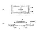
本発明の吸収型多層膜NDフィルターの製造に用いる装置は、例えば図4に示すように、スパッタリング室1内に、帯状樹脂フィルム基板2の巻取りと巻出しをする第1ロール3a及び第2ロール3bと、第1ロール3aと第2ロール3bの間に設けられ、帯状樹脂フィルム基板2を外周面に沿わせて移動させるキャンロール4と、酸化物誘電体膜層の成膜用ターゲットを備えた第1カソード5と、金属吸収膜層の成膜用ターゲットとを備えた第2カソード6とを具備するスパッタリングロールコータである。 For example, as shown in FIG. 4, the apparatus used for manufacturing the absorption multilayer ND filter of the present invention includes a
そして、上記キャンロール4と第2カソード6の間には、金属吸収膜層にフィルム搬送方向に対して垂直な方向に膜厚分布を施すことが可能な遮蔽マスク7を備えている。尚、酸化物誘電体膜層及び金属吸収膜層の成膜には、公知のスパッタリング法を用いることができる。例えば、マグネトロンスパッタリング法の場合、第1カソード及び第2カソードはスパッタリングターゲットを備え、イオンビームスパッタリング法の場合には第1カソード及び第2カソードはパッタリングターゲットと共にイオンビーム発生装置を備えている。 A shielding
上記の金属吸収膜層に膜厚分布を施す遮蔽マスクの具体例を、拡大して図5に示す。金属吸収膜層に膜厚分布を施す遮蔽マスク8は、図5(a)に示すように、その中央部に樹脂フィルム基板2の移動方向と平行に、矩形状の遮蔽部分8aを有している。この矩形状の遮蔽部分8aは、図5(a)の点線部分を拡大した図5(b)から分るように断面が台形状をなすことで樹脂フィルム基板側の幅が広くなるように加工されている。 A specific example of a shielding mask for applying a film thickness distribution to the metal absorption film layer is shown in FIG. As shown in FIG. 5A, the shielding
遮蔽マスク8が上記のごとく断面台形状の遮蔽部分8aを有することにより、遮蔽マスク8に対向する樹脂フィルム基板2上に形成される金属吸収膜層(例えばNi合金膜層)の膜厚を、位置Xの範囲(図中に矢印で示す金属吸収膜層膜厚ゼロ位置から最大膜厚までの範囲)において遮蔽部分8aの中心に近いほど薄くなるように制御することができ、樹脂フィルム基板と遮蔽マスクの隙間を小さくすることにより、グラデーション範囲を狭くすることができる。具体的には、グラデーション濃度分布を有する範囲が2〜20mmとすることができ、従来にない狭い範囲のグラデーション濃度分布を有する吸収型多層膜NDフィルターを得ることができる。 When the shielding
金属吸収膜層を成膜するためのスパッタリングターゲットには、NiあるいはNi合金のターゲットがある。尚、Ni合金としては、Ni−Ti(Ti量:8wt%)のほか、Al、V、W、Ta、Siから選ばれた1種類以上の元素を添加したものがある。また、酸化物誘電体膜層であるSiOx(ただし、1.8≦x≦2.0)を成膜するためのターゲットには、Si又はSiCターゲットを用いることができる。尚、酸化物誘電体膜層にはSiOx膜層が最も好ましいが、SiOx膜層に代えてAl2O3も使用することができる。また、光学特性の波長依存性を改善するためにTiO2、Nb2O3、Ta2O5、HfO2、ZrO2を添加することも可能である。As a sputtering target for forming the metal absorption film layer, there is a Ni or Ni alloy target. In addition, as Ni alloy, there is one in which one or more elements selected from Al, V, W, Ta, and Si are added in addition to Ni—Ti (Ti amount: 8 wt%). In addition, a Si or SiC target can be used as a target for depositing SiOx (where 1.8 ≦ x ≦ 2.0) which is an oxide dielectric film layer. The oxide dielectric film layer is most preferably a SiOx film layer, but Al2 O3 can also be used instead of the SiOx film layer. In addition, TiO2 , Nb2 O3 , Ta2 O5 , HfO2 , and ZrO2 can be added in order to improve the wavelength dependency of optical characteristics.
上記金属吸収膜層を成膜するためのスパッタリングターゲット、例えばNi合金ターゲットは、アルゴンガスを導入するマグネトロンスパッタリングあるいはイオンビームスパッタリングにより成膜することが好ましい。一方、酸化物誘電体膜層を成膜するためのスパッタリングターゲット、例えばSiOx膜層を成膜するためのSi又はSiCターゲットは、アルゴンガスを導入するデュアルマグネトロンスパッタリングにより成膜され、Si又はSiCターゲットからSiOxを成膜するためにインピーダンスモニターにより酸素導入量を制御して成膜することができる。 A sputtering target for forming the metal absorption film layer, for example, a Ni alloy target, is preferably formed by magnetron sputtering or ion beam sputtering into which argon gas is introduced. On the other hand, a sputtering target for forming an oxide dielectric film layer, for example, a Si or SiC target for forming a SiOx film layer, is formed by dual magnetron sputtering in which argon gas is introduced, and the Si or SiC target. In order to form a SiOx film, the oxygen introduction amount can be controlled by an impedance monitor.
例えば、金属吸収膜層を成膜する場合、Ni−Ti合金ターゲットを用いて、Arガスを導入するDCマグネトロンスパッタリングで成膜することができる。また、酸化物誘電体膜層であるSiOx膜層を成膜する場合には、SiCセラミックターゲットを用い、Arガスを導入するデュアルマグネトロンスパッタリングにより成膜することができる。その際、SiCからSiOxを成膜するためにインピーダンスモニター(例えば、ボンアルデンヌ社製プラズマエミッションモニター)により酸素導入量を制御する。 For example, when forming a metal absorption film layer, the film can be formed by DC magnetron sputtering in which Ar gas is introduced using a Ni—Ti alloy target. Further, when forming the SiOx film layer which is an oxide dielectric film layer, it can be formed by dual magnetron sputtering using an SiC ceramic target and introducing Ar gas. At that time, the amount of oxygen introduced is controlled by an impedance monitor (for example, a plasma emission monitor manufactured by Bon Ardennes) in order to form a SiOx film from SiC.
ここで、SiOx膜層に含まれる酸素量を1.8≦x≦2.0の範囲で調整するのは、波長400〜700nmにおける平均透過率(=(最大透過率−最小透過率)/平均透過率)を改善するためである。成膜中の酸素導入量を多くするほどxは大きくなり、可視波長域(400〜700nm)の短波長側の透過率が増加する傾向がある。一方、成膜中の酸素導入量を少なくするほどxは小さくなり、可視波長域(400〜700nm)の短波長側の透過率が減少する傾向がある。 Here, the amount of oxygen contained in the SiOx film layer is adjusted within the range of 1.8 ≦ x ≦ 2.0 in order to adjust the average transmittance (= (maximum transmittance−minimum transmittance) / average in the wavelength range of 400 to 700 nm. This is for improving the transmittance. As the amount of oxygen introduced during film formation increases, x increases and the transmittance on the short wavelength side in the visible wavelength region (400 to 700 nm) tends to increase. On the other hand, as the amount of oxygen introduced during film formation decreases, x decreases and the transmittance on the short wavelength side in the visible wavelength region (400 to 700 nm) tends to decrease.
本発明の膜構造の吸収型多層膜NDフィルターにおいて、Ni合金膜厚が厚く平均透過率が低い領域は可視波長域の短波長側の透過率が長波長側より高く、Ni合金膜厚が薄く平均透過率が高い領域は可視波長域の短波長側の透過率が長波長側より低い傾向にある。そこで、グラデーション濃度分布範囲の透過率の低い領域の透過率平坦性を重視するならば、成膜中の酸素導入量は少なくして短波長側の透過率を減少させた方が好ましく、逆に透過率の高い領域の透過率平坦性を重視するならば、成膜中の酸素導入量は多くして短波長側の透過率を減少させない方が好ましい。しかし、SiOxの酸素量xは最大2.0までが限界であり、xを1.8よりも少なくすると透過率が低い範囲においても短波長側の透過率が減少し過ぎてしまう。 In the absorptive multilayer ND filter having the film structure of the present invention, in the region where the Ni alloy film thickness is large and the average transmittance is low, the transmittance on the short wavelength side in the visible wavelength region is higher than that on the long wavelength side, and the Ni alloy film thickness is thin. In the region where the average transmittance is high, the transmittance on the short wavelength side in the visible wavelength region tends to be lower than that on the long wavelength side. Therefore, if importance is attached to the transmittance flatness in the low-transmission area of the gradation density distribution range, it is preferable to reduce the transmittance on the short wavelength side by reducing the amount of oxygen introduced during film formation. If importance is attached to transmittance flatness in a region with high transmittance, it is preferable that the amount of oxygen introduced during film formation is increased so as not to reduce the transmittance on the short wavelength side. However, the oxygen amount x of SiOx is limited to 2.0 at maximum, and if x is less than 1.8, the transmittance on the short wavelength side is excessively reduced even in a range where the transmittance is low.
吸収型多層膜NDフィルターに用いる樹脂フィルム基板については、例えば、ポリエチレンテレフタレート(PET)、ポリエーテルスルフォン(PES)、ポリアリレート(PAR)、ポリカーボネート(PC)、ポリオレフィン(PO)、ノルボルネンの樹脂材料から選択される樹脂フィルム単体、あるいは、これ等の樹脂フィルム単体の片面又は両面にアクリル系有機膜を設けた複合体を好適に使用することができる。特に、ノルボルネンの樹脂材料については、代表的なものとして日本ゼオン社のゼオノア(商品名)やJSR社のアートン(商品名)等が挙げられる。 About the resin film substrate used for the absorption type multilayer ND filter, for example, from a resin material of polyethylene terephthalate (PET), polyethersulfone (PES), polyarylate (PAR), polycarbonate (PC), polyolefin (PO), norbornene The selected resin film alone or a composite in which an acrylic organic film is provided on one or both surfaces of the resin film alone can be suitably used. In particular, as for the resin material of norbornene, representative examples include ZEONOR (trade name) manufactured by Nippon Zeon Co., Ltd. and Arton (trade name) manufactured by JSR Corporation.
上記樹脂フィルム基板の厚さは、50〜100μmであることが好ましい。樹脂フィルム基板の厚さが50μm未満であると、スパッタリング成膜の熱負荷に耐えることができずに、シワやウネリが発生するからである。また、樹脂フィルム基板の厚さが100μmを越えると、フィルムが厚すぎるために省スペースに組み込めないばかりか、成膜の際にフィルムを移動させるために大きな駆動力を必要とするため好ましくない。 The thickness of the resin film substrate is preferably 50 to 100 μm. This is because if the thickness of the resin film substrate is less than 50 μm, it cannot withstand the thermal load of sputtering film formation, and wrinkles and undulation are generated. In addition, if the thickness of the resin film substrate exceeds 100 μm, the film is too thick to be incorporated in a space-saving manner, and it is not preferable because a large driving force is required to move the film during film formation.
本発明による吸収型多層膜NDフィルターの製造方法について、図4を参照して説明する。ここでは、金属吸収膜層を成膜するためのスパッタリングターゲットとしてNi合金ターゲットを用い、酸化物誘電体膜層であるSiOxを成膜するためのスパッタリングターゲットとしてSiCターゲットを用いた場合を例に挙げて、吸収型多層膜の成膜手順を具体的に説明する。 A method for manufacturing the absorption multilayer ND filter according to the present invention will be described with reference to FIG. Here, as an example, a Ni alloy target is used as a sputtering target for forming a metal absorption film layer, and a SiC target is used as a sputtering target for forming SiOx as an oxide dielectric film layer. The procedure for forming the absorption multilayer film will be specifically described.
まず、図4の製造装置のスパッタリング室1を、1×10⁻⁴Pa程度まで排気する。そして、第1ロール3aから帯状樹脂フィルム基板2を巻出し、水冷されたキャンロール4を経て第2ロール3bに巻取る方向(正転方向)に搬送する。その際、フィルム搬送速度を、例えば1〜5m/min程度に調整する。その状態で、キャンロール4上で帯状フィルム基板8にSiOx膜層を成膜する。First, the sputtering
即ち、SiCターゲットが取付けられた第1カソード5を用い、アルゴンガスを導入した雰囲気中において、インピーダンスモニターにより酸素導入量を制御しながら、マグネトロンスパッタリングを行なうことにより酸化物誘電体膜層であるSiOx膜層を成膜する。キャンロール4と第1カソード5の間には遮蔽マスクが存在しないので、SiOx膜層の膜厚は常に一定となる。 That is, using the
次に、第2ロール3bに巻取られた帯状樹脂フィルム基板2を巻出し、キャンロール4を経て第1ロール3aに巻取る方向(逆転方向)に搬送する。そして、Ni合金ターゲットが取付けられた第2カソード6を使用し、アルゴンガスを導入した雰囲気中にてマグネトロンスパッタリングを行って、キャンロール4上にて帯状フィルム基板8に金属吸収膜層であるNi合金膜層を成膜する。キャンロール4と第2カソード6の間には遮蔽マスク8が設置してあるため、上記したようにNi合金膜層に所定の膜厚分布を施すことができる。 Next, the belt-shaped
また、遮蔽マスク8は、図5(b)にあるように、樹脂フィルム基板と遮蔽マスクの隙間によってグラデーション濃度分布範囲を調整することができる。両者の間隔を離せばグラデーション濃度分布範囲が広くなり、この間隔を狭くすればグラデーション濃度分布範囲も狭くすることができる。また、図5(b)に示すように、1本の遮蔽マスクの両側にグラデーション濃度分布を有する範囲が得られるわけであり、遮蔽マスクをN本配置すれば、それぞれの両側に合計2×N本のグラデーション濃度分布を有する範囲を得ることができる。 In addition, as shown in FIG. 5B, the gradation density distribution range of the shielding
以後、上記と同様に帯状樹脂フィルム基板2を正転方向及び逆転方向の順に搬送しながら、それぞれ所定の膜厚分布を有するSiOx膜層とNi合金膜層の成膜を繰り返し、酸化物誘電体膜層と金属吸収膜層が必要な層数だけ積層された吸収型多層膜を形成する。 Thereafter, the SiOx film layer and the Ni alloy film layer each having a predetermined film thickness distribution are repeatedly formed while the belt-shaped
また、必要に応じて、上記のごとく片面に吸収型多層膜の成膜が完了した帯状樹脂フィルム基板2を取り出し、表裏を反転させて第1ロール3aにセットし直した後、上記の工程を繰り返すことによって、帯状樹脂フィルム基板2の他面にも上記と同様の酸化物誘電体膜層であるSiOx膜層と金属吸収膜層であるNi合金膜層を成膜することができる。 In addition, if necessary, the belt-shaped
上述したように、一般的なスパッタリング法などの成膜方法では、樹脂フィルム基板に遮蔽マスクを直接取付けるため、酸化物誘電体膜層と金属吸収膜層のどちらか一方にのみ膜厚分布をつけることは極めて難しく、両方がほぼ同じ膜厚分布になってしまう。ところが、本発明によれば、スパッタリングロールコータを用いて樹脂フィルム基板をロール状態のまま成膜するので、片方のスパッタリングターゲット前面にのみ遮蔽マスクを配置することが可能であり、金属吸収膜層にのみ膜厚分布をつけることができる。 As described above, in a film forming method such as a general sputtering method, a shielding mask is directly attached to a resin film substrate, so that only one of the oxide dielectric film layer and the metal absorption film layer has a film thickness distribution. This is extremely difficult and both result in almost the same film thickness distribution. However, according to the present invention, since the resin film substrate is formed in a roll state using a sputtering roll coater, it is possible to arrange a shielding mask only on the front surface of one of the sputtering targets, and the metal absorption film layer. Only the film thickness distribution can be given.
また、一般的な成膜方法では、樹脂フィルム基板に遮蔽マスクを直接取付けるため、酸化物誘電体膜層と金属吸収膜層のどちらか一方にのみ膜厚分布をつけることは極めて難しく、両方がほぼ同じ膜厚分布になる。従って、金属吸収膜層の膜厚がゼロの部分は酸化物誘電体膜層の膜厚もゼロになり、樹脂フィルム基板(例えば、両面易接着層付PETフィルム表面の鉛筆硬度はHB)が露出している状態になる。 Moreover, in a general film formation method, since a shielding mask is directly attached to a resin film substrate, it is extremely difficult to provide a film thickness distribution on only one of the oxide dielectric film layer and the metal absorption film layer. The film thickness distribution is almost the same. Therefore, when the film thickness of the metal absorption film layer is zero, the film thickness of the oxide dielectric film layer is also zero, and the resin film substrate (for example, the pencil hardness of the surface of the PET film with a double-sided easy-adhesion layer is HB) is exposed. It will be in the state.
これに対し、本発明の吸収型多層膜NDフィルターは、金属吸収膜層のない部分でも所定膜厚の酸化物誘電体膜層(例えば、SiOx膜層であれば鉛筆硬度はH)が成膜されているため十分な硬度を有しており、駆動するNDフィルターが他部品に触れたとしても傷が付き難く、耐久性にも優れている。 On the other hand, the absorption type multilayer ND filter of the present invention forms an oxide dielectric film layer (for example, the pencil hardness is H in the case of a SiOx film layer) even in a portion where there is no metal absorption film layer. Therefore, it has sufficient hardness, and even if the ND filter to be driven touches other parts, it is difficult to be scratched and has excellent durability.
上記した遮蔽マスクを備えるロールトゥロールプロセスのスパッタリングロールコータを用いる製造方法により、酸化物誘電体膜層の膜厚は均一で且つ金属吸収膜層の膜厚のみ膜厚分布を施したグラデーション濃度分布を有するNDフィルターを製造することができる。しかも、グラデーション濃度分布の範囲(幅)を従来よりも狭くすることができ、撮影画像の色調に影響も極めて小さく、特にデジタルビデオカメラを初めとする動画撮影機器への搭載用として極めて優れている。 A gradation concentration distribution in which the oxide dielectric film layer has a uniform film thickness and only the metal absorption film thickness is distributed by the manufacturing method using the sputtering roll coater of the roll-to-roll process including the shielding mask described above. An ND filter having the following can be manufactured. In addition, the gradation density distribution range (width) can be made narrower than before, and the influence on the color tone of the photographed image is extremely small, and it is particularly excellent for use in video camera equipment such as digital video cameras. .
[実施例1]
図4に示す樹脂フィルム基板をロール状態のまま成膜することが可能なスパッタリングロールコータによる製造装置により、図5に示すNi合金膜層に膜厚分布を与える第2遮蔽マスクを配置して、グラデーション濃度分布を有する吸収型多層膜NDフィルターを製造した。尚、樹脂フィルム基板には、厚さ100μmの両面易接着層付PETフィルムを用いた。[Example 1]
With a manufacturing apparatus using a sputtering roll coater capable of forming the resin film substrate shown in FIG. 4 in a roll state, a second shielding mask that gives a film thickness distribution to the Ni alloy film layer shown in FIG. An absorption multilayer ND filter having a gradation density distribution was manufactured. The resin film substrate used was a PET film with a double-sided easy-adhesion layer having a thickness of 100 μm.
Ni合金膜層に膜厚分布を与える遮蔽マスクは、図5に示すように、中央部に樹脂フィルム基板の移動方向と平行に、幅が50mmの矩形状の遮蔽部分有し、且つ矩形状の遮蔽部分は断面が台形状に形成してある。樹脂フィルム基板と遮蔽マスクの距離を増減させることにより、Ni合金膜層の膜厚分布を調整することができる。また、Ni合金膜層の膜厚分布は、導入するArガスの量や分圧によっても変わることがある。 As shown in FIG. 5, the shielding mask that gives the Ni alloy film layer a film thickness distribution has a rectangular shielding portion with a width of 50 mm in parallel with the moving direction of the resin film substrate at the center, and has a rectangular shape. The shield part has a trapezoidal cross section. The film thickness distribution of the Ni alloy film layer can be adjusted by increasing or decreasing the distance between the resin film substrate and the shielding mask. Further, the film thickness distribution of the Ni alloy film layer may vary depending on the amount of Ar gas introduced and the partial pressure.
本実施例では、Ni合金膜層に膜厚分布を与える遮蔽マスクと樹脂フィルム基板との距離を3mm、5mm、7mmに調整して、図1に示す膜構造を有する吸収型多層膜をそれぞれ成膜した。即ち、スパッタリング室に樹脂フィルム基板(幅300mm)をセットした後、1×10⁻⁴Paまで排気し、下記表2に示す条件にて吸収型多層膜の成膜を行った。樹脂フィルム基板の片面の成膜が終了した後、樹脂フィルム基板を裏返してセットし、上記と同じ条件で他面にも吸収型多層膜の成膜を行った。In this example, the distance between the shielding mask that gives the film thickness distribution to the Ni alloy film layer and the resin film substrate is adjusted to 3 mm, 5 mm, and 7 mm, respectively, thereby forming the absorption multilayer films having the film structure shown in FIG. Filmed. That is, after setting a resin film substrate (300 mm in width) in the sputtering chamber, it was evacuated to 1 × 10⁻⁴ Pa, and an absorption multilayer film was formed under the conditions shown in Table 2 below. After the film formation on one side of the resin film substrate was completed, the resin film substrate was turned over and set, and an absorption multilayer film was formed on the other surface under the same conditions as described above.
得られた各吸収型多層膜NDフィルターについて、顕微分光装置を用いて、それぞれ分光透過特性の評価を行った。即ち、Ni合金膜層の膜厚が0nmの位置を原点(0mm)として1mm間隔で位置Xごとに分光透過率を測定した。 About each obtained absorption type multilayer ND filter, the spectral transmission characteristic was each evaluated using the microspectroscope. That is, the spectral transmittance was measured for each position X at 1 mm intervals with the origin (0 mm) being the position where the film thickness of the Ni alloy film layer was 0 nm.
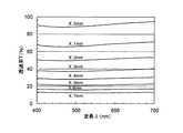
遮蔽マスクと樹脂フィルム基板との距離を5mmに設定して得られた吸収型多層膜NDフィルターの結果を図3に示した。この吸収型多層膜NDフィルターのグラデーション濃度分布はX=0mmの位置から透過率が最小値とほぼ同じ値となる位置までであり、グラデーション濃度分布の範囲(幅)は約7mmであることが分る。 The result of the absorption multilayer ND filter obtained by setting the distance between the shielding mask and the resin film substrate to 5 mm is shown in FIG. The gradation density distribution of this absorption multilayer ND filter is from the position where X = 0 mm to the position where the transmittance is almost the same as the minimum value, and the gradation density distribution range (width) is about 7 mm. The
また、遮蔽マスクと樹脂フィルム基板の間隔が3mm、5mm、7mmの各吸収型多層膜NDフィルターについて、波長550nmにおける透過率変化を図6に示す。図6に示す結果から、吸収型多層膜NDフィルターのグラデーション濃度分布の範囲(幅)は、それぞれ約5mm、約7mm、約9mmであることが分る。 FIG. 6 shows the change in transmittance at a wavelength of 550 nm for each of the absorption multilayer ND filters having a distance of 3 mm, 5 mm, and 7 mm between the shielding mask and the resin film substrate. From the results shown in FIG. 6, it can be seen that the gradation density distribution ranges (widths) of the absorption multilayer ND filter are about 5 mm, about 7 mm, and about 9 mm, respectively.
このように、フィルム搬送方向と平行な遮蔽部分を有する遮蔽マスクを用いても、Ni合金膜に膜厚分布を与える遮蔽マスクと樹脂フィルム基板との間隔を適切に選択することで、Ni合金膜の回り込みを制御することができ、吸収型多層膜NDフィルターのグラデーション濃度分布の範囲(幅)を変化させることができる。また、遮蔽マスクがフィルム搬送方向と平行なため、グラデーション濃度分布の範囲は遮蔽マスクと樹脂フィルム基板の間隔のみにより制御され、グラデーション濃度分布が遮蔽マスク自体とその形状(三角や階段状)により2重になることはない。 Thus, even when a shielding mask having a shielding part parallel to the film conveyance direction is used, the Ni alloy film can be selected by appropriately selecting the interval between the shielding mask that gives the Ni alloy film a film thickness distribution and the resin film substrate. Can be controlled, and the range (width) of the gradation density distribution of the absorption multilayer ND filter can be changed. In addition, since the shielding mask is parallel to the film transport direction, the gradation density distribution range is controlled only by the distance between the shielding mask and the resin film substrate, and the gradation density distribution is 2 depending on the shielding mask itself and its shape (triangle or step shape). There is no overlap.
1 スパッタリング室
2 帯状樹脂フィルム基板
3a 第1ロール
3b 第2ロール
4 キャンロール
5 第1カソード
6 第2カソード
8 第2遮蔽マスクDESCRIPTION OF
Claims (4)
Translated fromJapaneseスパッタリング室内に、帯状樹脂フィルム基板の巻取りと巻出しをする第1ロール及び第2ロールと、第1ロールと第2ロールの間に設けられ帯状樹脂フィルム基板を外周面に沿わせて移動させるキャンロールと、酸化物誘電体膜層の成膜用ターゲットを備えた第1カソードと、金属吸収膜層の成膜用ターゲットを備えた第2カソードとを具備するスパッタリング成膜装置を使用し、
前記第1ロール又は第2ロールから巻出されてキャンロール外周面に沿って搬送される帯状樹脂フィルム基板に対し、第1カソードを用いて酸化物誘電体膜層の成膜を行いながら第2ロール又は第1ロールに帯状樹脂フィルム基板を巻き取った後、
第1ロール、第2ロール並びにキャンロールの各回転方向を反転させ、且つキャンロール外周面に沿って搬送される帯状樹脂フィルム基板に対し、キャンロールと第2カソードの間に設けた金属吸収膜層にフィルム搬送方向と垂直方向に膜厚分布を施す遮蔽マスクを介して、第2カソードを用いて金属吸収膜層の成膜を行いながら第1ロール又は第2ロールに帯状樹脂フィルム基板を巻取り、
引き続き上記一連の工程を繰り返して吸収型多層膜を形成することを特徴とする吸収型多層膜NDフィルターの製造方法。Gradation density distribution with an absorption multilayer film in which oxide dielectric film layers and metal absorption film layers are alternately laminated on at least one surface of a resin film substrate, and the transmittance gradually decreases as the distance from the optical axis center increases. A method for producing an absorption-type multilayer ND filter having
The first and second rolls for winding and unwinding the belt-shaped resin film substrate and the belt-shaped resin film substrate provided between the first and second rolls are moved along the outer peripheral surface in the sputtering chamber. Using a sputtering film forming apparatus comprising a can roll, a first cathode provided with a target for forming an oxide dielectric film layer, and a second cathode provided with a target for forming a metal absorbing film layer,
While forming the oxide dielectric film layer on the belt-shaped resin film substrate unwound from the first roll or the second roll and conveyed along the outer peripheral surface of the can roll, the second film is formed using the first cathode. After winding the belt-shaped resin film substrate on the roll or the first roll,
A metal absorbing film provided between the can roll and the second cathode with respect to the belt-shaped resin film substrate that reverses the rotation directions of the first roll, the second roll, and the can roll and is conveyed along the outer peripheral surface of the can roll. A belt-shaped resin film substrate is wound around the first roll or the second roll while forming the metal absorbing film layer using the second cathode through a shielding mask that gives a film thickness distribution in the direction perpendicular to the film transport direction to the layer. take,
Subsequently, the above series of steps are repeated to form an absorption multilayer film, and a method for producing an absorption multilayer film ND filter is provided.
Priority Applications (1)
| Application Number | Priority Date | Filing Date | Title |
|---|---|---|---|
| JP2008303845AJP2010128259A (en) | 2008-11-28 | 2008-11-28 | Absorption type multilayer film nd filter and method of manufacturing the same |
Applications Claiming Priority (1)
| Application Number | Priority Date | Filing Date | Title |
|---|---|---|---|
| JP2008303845AJP2010128259A (en) | 2008-11-28 | 2008-11-28 | Absorption type multilayer film nd filter and method of manufacturing the same |
Publications (1)
| Publication Number | Publication Date |
|---|---|
| JP2010128259Atrue JP2010128259A (en) | 2010-06-10 |
Family
ID=42328690
Family Applications (1)
| Application Number | Title | Priority Date | Filing Date |
|---|---|---|---|
| JP2008303845APendingJP2010128259A (en) | 2008-11-28 | 2008-11-28 | Absorption type multilayer film nd filter and method of manufacturing the same |
Country Status (1)
| Country | Link |
|---|---|
| JP (1) | JP2010128259A (en) |
Cited By (7)
| Publication number | Priority date | Publication date | Assignee | Title |
|---|---|---|---|---|
| WO2015195123A1 (en) | 2014-06-18 | 2015-12-23 | Jds Uniphase Corporation | Metal-dielectric optical filter, sensor device, and fabrication method |
| US10197716B2 (en) | 2012-12-19 | 2019-02-05 | Viavi Solutions Inc. | Metal-dielectric optical filter, sensor device, and fabrication method |
| US10222523B2 (en) | 2012-12-19 | 2019-03-05 | Viavi Solutions Inc. | Sensor device including one or more metal-dielectric optical filters |
| US10378955B2 (en) | 2012-12-19 | 2019-08-13 | Viavi Solutions Inc. | Spectroscopic assembly and method |
| JP2020134571A (en)* | 2019-02-14 | 2020-08-31 | キヤノン株式会社 | Optical elements, optics, imaging devices, and lens devices |
| JP2021100138A (en)* | 2019-04-02 | 2021-07-01 | ヴァイアヴィ・ソリューションズ・インコーポレイテッドViavi Solutions Inc. | Metal-dielectric optical filter, sensor device, and fabrication method |
| WO2022179742A1 (en)* | 2021-02-25 | 2022-09-01 | Ams-Osram Ag | Method of manufacturing an optical element |
Citations (5)
| Publication number | Priority date | Publication date | Assignee | Title |
|---|---|---|---|---|
| JP2003322709A (en)* | 2002-04-30 | 2003-11-14 | Sony Corp | Thin film type nd filter |
| JP2007199447A (en)* | 2006-01-27 | 2007-08-09 | Canon Electronics Inc | Nd filter, its manufacturing method, and light quantity reducing device |
| JP2008070432A (en)* | 2006-09-12 | 2008-03-27 | Sumitomo Metal Mining Co Ltd | Method for manufacturing absorption multilayer ND filter |
| JP2008112034A (en)* | 2006-10-31 | 2008-05-15 | Canon Electronics Inc | ND filter |
| JP2008276112A (en)* | 2007-05-07 | 2008-11-13 | Canon Electronics Inc | Nd filter |
- 2008
- 2008-11-28JPJP2008303845Apatent/JP2010128259A/enactivePending
Patent Citations (5)
| Publication number | Priority date | Publication date | Assignee | Title |
|---|---|---|---|---|
| JP2003322709A (en)* | 2002-04-30 | 2003-11-14 | Sony Corp | Thin film type nd filter |
| JP2007199447A (en)* | 2006-01-27 | 2007-08-09 | Canon Electronics Inc | Nd filter, its manufacturing method, and light quantity reducing device |
| JP2008070432A (en)* | 2006-09-12 | 2008-03-27 | Sumitomo Metal Mining Co Ltd | Method for manufacturing absorption multilayer ND filter |
| JP2008112034A (en)* | 2006-10-31 | 2008-05-15 | Canon Electronics Inc | ND filter |
| JP2008276112A (en)* | 2007-05-07 | 2008-11-13 | Canon Electronics Inc | Nd filter |
Cited By (15)
| Publication number | Priority date | Publication date | Assignee | Title |
|---|---|---|---|---|
| US10670455B2 (en) | 2012-12-19 | 2020-06-02 | Viavi Solutions Inc. | Spectroscopic assembly and method |
| US11782199B2 (en) | 2012-12-19 | 2023-10-10 | Viavi Solutions Inc. | Metal-dielectric optical filter, sensor device, and fabrication method |
| US10197716B2 (en) | 2012-12-19 | 2019-02-05 | Viavi Solutions Inc. | Metal-dielectric optical filter, sensor device, and fabrication method |
| US10222523B2 (en) | 2012-12-19 | 2019-03-05 | Viavi Solutions Inc. | Sensor device including one or more metal-dielectric optical filters |
| US10378955B2 (en) | 2012-12-19 | 2019-08-13 | Viavi Solutions Inc. | Spectroscopic assembly and method |
| US12366692B2 (en) | 2012-12-19 | 2025-07-22 | Viavi Solutions Inc. | Metal-dielectric optical filter, sensor device, and fabrication method |
| US10928570B2 (en) | 2012-12-19 | 2021-02-23 | Viavi Solutions Inc. | Metal-dielectric optical filter, sensor device, and fabrication method |
| JP2017526945A (en)* | 2014-06-18 | 2017-09-14 | ヴァイアヴィ・ソリューションズ・インコーポレイテッドViavi Solutions Inc. | Metal dielectric optical filter, sensor device, and manufacturing method |
| KR20170020886A (en)* | 2014-06-18 | 2017-02-24 | 비아비 솔루션즈 아이엔씨. | Metal-dielectric optical filter, sensor device, and fabrication method |
| WO2015195123A1 (en) | 2014-06-18 | 2015-12-23 | Jds Uniphase Corporation | Metal-dielectric optical filter, sensor device, and fabrication method |
| KR102240253B1 (en) | 2014-06-18 | 2021-04-13 | 비아비 솔루션즈 아이엔씨. | Metal-dielectric optical filter, sensor device, and fabrication method |
| EP3158371B1 (en)* | 2014-06-18 | 2025-04-23 | Viavi Solutions Inc. | Fabrication method of a metal-dielectric optical filter |
| JP2020134571A (en)* | 2019-02-14 | 2020-08-31 | キヤノン株式会社 | Optical elements, optics, imaging devices, and lens devices |
| JP2021100138A (en)* | 2019-04-02 | 2021-07-01 | ヴァイアヴィ・ソリューションズ・インコーポレイテッドViavi Solutions Inc. | Metal-dielectric optical filter, sensor device, and fabrication method |
| WO2022179742A1 (en)* | 2021-02-25 | 2022-09-01 | Ams-Osram Ag | Method of manufacturing an optical element |
Similar Documents
| Publication | Publication Date | Title |
|---|---|---|
| JP4595687B2 (en) | Absorption-type multilayer ND filter | |
| JP4984101B2 (en) | Method for manufacturing absorption multilayer ND filter | |
| JP2010128259A (en) | Absorption type multilayer film nd filter and method of manufacturing the same | |
| JP4613706B2 (en) | Absorption-type multilayer ND filter | |
| JPWO2012157706A1 (en) | Optical filter, optical device, electronic device, and antireflection composite | |
| JP2005326687A (en) | Nd filter and light quantity diaphragm device | |
| JP2004354735A (en) | Ray cut filter | |
| JP2008139693A (en) | Infrared cut filter | |
| JP5051361B2 (en) | Absorption type multilayer ND filter manufacturing apparatus and method for manufacturing absorption type multilayer ND filter using the apparatus | |
| JP2013225105A (en) | Method for producing optical thin film, and absorptive multilayered film nd filter | |
| JP2003322709A (en) | Thin film type nd filter | |
| JP2010224350A (en) | Absorption-type multilayer ND filter and manufacturing method thereof | |
| JP4963027B2 (en) | ND filter, method for manufacturing the same, and light quantity reduction device using them | |
| JP2003207608A (en) | Nd filter and its manufacturing method, and imaging device | |
| JP2008008975A (en) | Nd filter, light quantity regulator, lens barrel and image pickup apparatus | |
| KR102567493B1 (en) | Mask blanks and photomask | |
| JP2010128258A (en) | Absorption type multilayer film nd filter and method of manufacturing the same | |
| JP2011118251A (en) | Method for manufacturing nd filter and nd filter | |
| JP4862829B2 (en) | Absorption-type multilayer ND filter | |
| JP5104620B2 (en) | Absorption-type multilayer ND filter, manufacturing apparatus therefor, and method for manufacturing absorption-type multilayer ND filter | |
| JP4466457B2 (en) | Absorption-type multilayer ND filter and manufacturing method thereof | |
| JP4914954B2 (en) | ND filter | |
| JP2011059299A (en) | Absorption-type multilayer film nd (neutral density) filter, and method of manufacturing the same | |
| JP2014016568A (en) | Absorption type multilayer film nd filter | |
| JP4984100B2 (en) | Method for manufacturing absorption multilayer ND filter |
Legal Events
| Date | Code | Title | Description |
|---|---|---|---|
| A621 | Written request for application examination | Free format text:JAPANESE INTERMEDIATE CODE: A621 Effective date:20110422 | |
| A977 | Report on retrieval | Free format text:JAPANESE INTERMEDIATE CODE: A971007 Effective date:20120509 | |
| A131 | Notification of reasons for refusal | Free format text:JAPANESE INTERMEDIATE CODE: A131 Effective date:20120904 | |
| A521 | Written amendment | Free format text:JAPANESE INTERMEDIATE CODE: A523 Effective date:20121022 | |
| A131 | Notification of reasons for refusal | Free format text:JAPANESE INTERMEDIATE CODE: A131 Effective date:20130319 | |
| A02 | Decision of refusal | Free format text:JAPANESE INTERMEDIATE CODE: A02 Effective date:20130917 |