JP2010115056A - Power supply system and vehicle - Google Patents
Power supply system and vehicleDownload PDFInfo
- Publication number
- JP2010115056A JP2010115056AJP2008286849AJP2008286849AJP2010115056AJP 2010115056 AJP2010115056 AJP 2010115056AJP 2008286849 AJP2008286849 AJP 2008286849AJP 2008286849 AJP2008286849 AJP 2008286849AJP 2010115056 AJP2010115056 AJP 2010115056A
- Authority
- JP
- Japan
- Prior art keywords
- voltage
- current
- storage device
- power storage
- power
- Prior art date
- Legal status (The legal status is an assumption and is not a legal conclusion. Google has not performed a legal analysis and makes no representation as to the accuracy of the status listed.)
- Withdrawn
Links
Images


Classifications
- Y—GENERAL TAGGING OF NEW TECHNOLOGICAL DEVELOPMENTS; GENERAL TAGGING OF CROSS-SECTIONAL TECHNOLOGIES SPANNING OVER SEVERAL SECTIONS OF THE IPC; TECHNICAL SUBJECTS COVERED BY FORMER USPC CROSS-REFERENCE ART COLLECTIONS [XRACs] AND DIGESTS
- Y02—TECHNOLOGIES OR APPLICATIONS FOR MITIGATION OR ADAPTATION AGAINST CLIMATE CHANGE
- Y02T—CLIMATE CHANGE MITIGATION TECHNOLOGIES RELATED TO TRANSPORTATION
- Y02T10/00—Road transport of goods or passengers
- Y02T10/60—Other road transportation technologies with climate change mitigation effect
- Y02T10/62—Hybrid vehicles
- Y—GENERAL TAGGING OF NEW TECHNOLOGICAL DEVELOPMENTS; GENERAL TAGGING OF CROSS-SECTIONAL TECHNOLOGIES SPANNING OVER SEVERAL SECTIONS OF THE IPC; TECHNICAL SUBJECTS COVERED BY FORMER USPC CROSS-REFERENCE ART COLLECTIONS [XRACs] AND DIGESTS
- Y02—TECHNOLOGIES OR APPLICATIONS FOR MITIGATION OR ADAPTATION AGAINST CLIMATE CHANGE
- Y02T—CLIMATE CHANGE MITIGATION TECHNOLOGIES RELATED TO TRANSPORTATION
- Y02T10/00—Road transport of goods or passengers
- Y02T10/80—Technologies aiming to reduce greenhouse gasses emissions common to all road transportation technologies
- Y02T10/92—Energy efficient charging or discharging systems for batteries, ultracapacitors, supercapacitors or double-layer capacitors specially adapted for vehicles
Landscapes
- Hybrid Electric Vehicles (AREA)
- Charge And Discharge Circuits For Batteries Or The Like (AREA)
- Dc-Dc Converters (AREA)
Abstract
Translated fromJapaneseDescription
Translated fromJapanese本発明は電源システムおよび車両に関し、特に、蓄電装置と、蓄電装置と電力を授受する負荷装置との間に設けられる電圧変換器とを備える電源システムの制御技術に関する。 The present invention relates to a power supply system and a vehicle, and more particularly, to a control technique for a power supply system including a power storage device and a voltage converter provided between the power storage device and a load device that exchanges power.
コンバータ(DC/AC変換器)、インバータ(AC/DC変換器)等の電力変換器においては、一般に2つのスイッチング素子を正負極間に直列接続した構成が採用される。上下のスイッチング素子が同時にオンすると正負極間が短絡されてしまうため、これを避ける必要がある。そこで上下のスイッチング素子をオンオフ制御する際には、これらがともにオフ状態である期間を設ける必要がある。この期間は一般的に「デッドタイム」と呼ばれる。 In power converters such as converters (DC / AC converters) and inverters (AC / DC converters), generally a configuration in which two switching elements are connected in series between positive and negative electrodes is adopted. If the upper and lower switching elements are turned on at the same time, the positive and negative electrodes are short-circuited. Therefore, when the on / off control of the upper and lower switching elements is performed, it is necessary to provide a period in which both are in the off state. This period is commonly referred to as “dead time”.
デッドタイムに関連する電圧変換器の制御に関する技術がこれまでに提案されている。たとえば特開2008−48472号公報(特許文献1)は、適切なデッドタイム補償が可能な電力変換回路を開示する。特許文献1によれば、PWM(Pulse Width Modulation)制御器は、デッドタイム補償器から供給される信号に応じて、デッドタイムの電流方向から、三角波と比較する指令電圧を補正し、上下2つのスイッチング素子のデューティ比を変更してデッドタイム補償を行なう。
蓄電装置と、その蓄電装置に蓄えられた直流電力を交流電力に変換するインバータと、そのインバータからの交流電力により駆動力を発生するモータとを備えた車両が知られている。このような車両には、たとえばモータに加えて内燃機関を動力源として備えるハイブリッド車両、モータのみを動力源として備える電気自動車などがある。これらの車両においては、減速時にモータを発電機として用いることで、運動エネルギーを電気エネルギーに変換して、蓄電装置に蓄える「回生ブレーキ」が利用できる。 2. Description of the Related Art A vehicle is known that includes a power storage device, an inverter that converts DC power stored in the power storage device into AC power, and a motor that generates driving force using AC power from the inverter. Such vehicles include, for example, hybrid vehicles that include an internal combustion engine as a power source in addition to a motor, and electric vehicles that include only a motor as a power source. In these vehicles, a “regenerative brake” that converts kinetic energy into electrical energy and stores it in a power storage device by using a motor as a generator during deceleration can be used.
さらに、上記車両において蓄電装置の電圧を昇圧してインバータに供給する構成が採用されている。この構成によればモータを高電圧で駆動可能であるので、モータの高出力化を実現できる。モータの回生時には、モータによる発電電力は降圧されて蓄電装置に供給される。 Further, a configuration is adopted in which the voltage of the power storage device is boosted and supplied to the inverter in the vehicle. According to this configuration, since the motor can be driven with a high voltage, high output of the motor can be realized. During motor regeneration, the electric power generated by the motor is stepped down and supplied to the power storage device.
車両駆動用のモータと蓄電装置との間で電力が授受されるため、蓄電装置には電流の入出力が発生する。ここで蓄電装置から電流が出力される場合の電流の向き(すなわち蓄電装置からコンバータへの向き)を正とし、蓄電装置に電流が入力される場合の電流の向き(すなわちコンバータから蓄電装置への向き)を負とする。蓄電装置に流れる電流がゼロクロスする場合においては、コンバータの動作が降圧動作から昇圧動作に切換るため、コンバータに含まれる2つのスイッチング素子のデューティ比を適切に切換える必要が生じると考えられる。 Since electric power is transferred between the motor for driving the vehicle and the power storage device, current input / output occurs in the power storage device. Here, the current direction when current is output from the power storage device (ie, the direction from the power storage device to the converter) is positive, and the current direction when current is input to the power storage device (ie, from the converter to the power storage device). Direction) is negative. When the current flowing through the power storage device crosses zero, the operation of the converter is switched from the step-down operation to the step-up operation, so that it is considered necessary to appropriately switch the duty ratio of the two switching elements included in the converter.
特開2008−48472号公報には、蓄電装置に流れる電流の方向が正の場合、および負の場合の各々におけるスイッチング素子の制御は示されているものの、電流の方向が変化する場合におけるスイッチング素子の制御については開示されていない。 Japanese Patent Application Laid-Open No. 2008-48472 discloses the control of the switching element when the direction of the current flowing through the power storage device is positive and negative, but the switching element when the direction of the current changes No control is disclosed.
本発明の目的は、蓄電装置の電流の流れる方向が変化する場合に、蓄電装置に対応して設けられるコンバータのスイッチング素子を適切に制御することが可能な電源システム、およびそれを備える車両を提供することである。 An object of the present invention is to provide a power supply system capable of appropriately controlling a switching element of a converter provided corresponding to a power storage device when the direction of current flow of the power storage device changes, and a vehicle including the same It is to be.
本発明は要約すれば、電源システムであって、直流電力を授受可能な負荷装置に接続される正極ラインおよび負極ラインと、正極ラインおよび負極ラインに接続されるコンデンサと、負荷装置に対して直流電力を入出力する蓄電装置と、電圧変換装置と、制御装置とを備える。電圧変換装置は、正極ラインおよび負極ライン間に直列接続された上アーム素子および下アーム素子と、上アーム素子および下アーム素子の接続点と蓄電装置との間の電流経路に介挿接続されるリアクトルとを含む。電圧変換装置は、蓄電装置の第1の電圧と正極ラインおよび負極ライン間の第2の電圧とを相互に変換する。制御装置は、上アーム素子および下アーム素子が同時にオフするデッドタイムが存在するように上アーム素子および下アーム素子のスイッチング動作を制御する。制御装置は、第2の電圧が目標電圧より低下した場合には、上アーム素子のデューティ比を低下させることにより第2の電圧を上昇させる。制御装置は、蓄電装置に流れる電流の向きが、電圧変換装置から蓄電装置への向きである負方向から負方向と逆の正方向に変化した場合には、負方向から正方向への電流の向きの変化が生じない通常時に比較して、第2の電圧を上昇させるためのデューティ比の低下を制限する。 In summary, the present invention is a power supply system, a positive line and a negative line connected to a load device capable of transmitting and receiving DC power, a capacitor connected to a positive line and a negative line, and a direct current to the load device. A power storage device that inputs and outputs power, a voltage conversion device, and a control device are provided. The voltage conversion device is inserted and connected to an upper arm element and a lower arm element connected in series between the positive electrode line and the negative electrode line, and a current path between a connection point of the upper arm element and the lower arm element and the power storage device. Including reactors. The voltage conversion device mutually converts the first voltage of the power storage device and the second voltage between the positive electrode line and the negative electrode line. The control device controls the switching operation of the upper arm element and the lower arm element so that there is a dead time in which the upper arm element and the lower arm element are simultaneously turned off. When the second voltage falls below the target voltage, the control device raises the second voltage by reducing the duty ratio of the upper arm element. When the direction of the current flowing through the power storage device changes from the negative direction, which is the direction from the voltage conversion device to the power storage device, to the positive direction opposite to the negative direction, the control device changes the current from the negative direction to the positive direction. Compared to the normal time when the direction does not change, the reduction of the duty ratio for increasing the second voltage is limited.
制御装置は、電流の向きが負方向から正方向に変化した場合には、所定期間、デューティ比の下限値を、通常時におけるデューティ比の下限値よりも高く設定する。 When the current direction changes from the negative direction to the positive direction, the control device sets the lower limit value of the duty ratio to be higher than the lower limit value of the duty ratio in a normal period for a predetermined period.
制御装置は、電流の向きが負方向から正方向に変化した場合には、所定期間、デューティ比の低下率を、通常時におけるデューティ比の低下率に比べて小さく設定する。 When the direction of the current changes from the negative direction to the positive direction, the control device sets the rate of decrease of the duty ratio to be smaller than the rate of decrease of the duty ratio during normal time for a predetermined period.
本発明の他の局面に従うと車両であって、上記のいずれかに記載の電源システムと、電源システムと直流電力を授受する負荷装置とを備える。 According to another aspect of the present invention, a vehicle includes the power supply system according to any one of the above and a load device that exchanges DC power with the power supply system.
本発明によれば、蓄電装置の電流の流れる方向が変化する場合において、コンバータのスイッチング素子を適切に制御することが可能になる。 ADVANTAGE OF THE INVENTION According to this invention, when the direction through which the electric current of an electrical storage apparatus changes changes, it becomes possible to control the switching element of a converter appropriately.
以下に本発明の実施の形態について図面を参照して詳細に説明する。なお、以下図中における同一または相当部分には同一の符号を付してその説明は繰返さない。 Embodiments of the present invention will be described below in detail with reference to the drawings. In the following, the same or corresponding parts in the drawings are denoted by the same reference numerals and description thereof will not be repeated.
[実施の形態1]
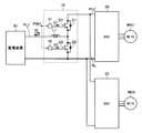
図1は、本発明の実施の形態1による電源システムを搭載した車両の一例として示されるハイブリッド車両の全体ブロック図である。図1を参照して、このハイブリッド車両1000は、エンジン2と、モータジェネレータMG1,MG2と、動力分割機構4と、車輪6とを備える。また、ハイブリッド車両1000は、蓄電装置B1と、コンバータ10と、コンデンサCと、インバータ20,22と、ECU(Electronic Control Unit)100とをさらに備える。[Embodiment 1]
FIG. 1 is an overall block diagram of a hybrid vehicle shown as an example of a vehicle equipped with a power supply system according to Embodiment 1 of the present invention. Referring to FIG. 1,
なお、コンバータ10は、本発明における「電圧変換装置」に対応する。また、インバータ20,22およびモータジェネレータMG1,MG2は、この発明における「負荷装置」を構成する。また、蓄電装置B1、コンバータ10、コンデンサC、これらに付随するセンサ、制御要素によって、本発明の「電源システム」が構成される。 Converter 10 corresponds to a “voltage conversion device” in the present invention.
ハイブリッド車両1000は、エンジン2およびモータジェネレータMG2を動力源として走行する。動力分割機構4は、エンジン2とモータジェネレータMG1,MG2とに結合されてこれらの間で動力を分配する。動力分割機構4は、たとえば、サンギヤ、プラネタリキャリヤおよびリングギヤの3つの回転軸を有する遊星歯車機構から成り、この3つの回転軸がエンジン2およびモータジェネレータMG1,MG2の回転軸にそれぞれ接続される。なお、モータジェネレータMG1のロータを中空にしてその中心にエンジン2のクランク軸を通すことにより、エンジン2およびモータジェネレータMG1,MG2を動力分割機構4に機械的に接続することができる。また、モータジェネレータMG2の回転軸は、図示されない減速ギヤや作動ギヤによって車輪6に結合される。
そして、モータジェネレータMG1は、エンジン2によって駆動される発電機として動作し、かつ、エンジン2の始動を行ない得る電動機として動作するものとしてハイブリッド車両1000に組込まれる。モータジェネレータMG2は、車輪6を駆動する電動機としてハイブリッド車両1000に組込まれる。 Motor generator MG1 is incorporated in
蓄電装置B1は、充放電可能な直流電源であり、たとえば、ニッケル水素やリチウムイオン等の二次電池、大容量のキャパシタ等から成る。蓄電装置B1は、コンバータ10へ電力を供給し、また、電力回生時には、コンバータ10によって充電される。 The power storage device B1 is a DC power source that can be charged and discharged, and includes, for example, a secondary battery such as nickel metal hydride or lithium ion, a large-capacity capacitor, and the like. Power storage device B1 supplies power to converter 10 and is charged by
コンバータ10は、ECU100からの信号PWCに基づいて蓄電装置B1からの電圧を昇圧し、その昇圧した電圧を正極ラインPL2へ出力する。また、コンバータ10は、インバータ20,22から正極ラインPL2を介して供給される回生電力を信号PWCに基づいて蓄電装置B1の電圧レベルに降圧し、蓄電装置B1を充電する。 Converter 10 boosts the voltage from power storage device B1 based on signal PWC from
コンデンサCは、正極ラインPL2と負極ラインNLとの間に接続され、正極ラインPL2と負極ラインNLとの間の電圧変動を平滑化する。正極ラインPL2および負極ラインNLの間の直流電圧VHは、蓄電装置B1およびコンバータ10によって構成される「電源システム」から、インバータ20,22およびモータジェネレータMG1,MG2による「負荷装置」への出力電圧に相当する。この直流電圧VHについて、以下では、システム電圧VHとも称する。 Capacitor C is connected between positive electrode line PL2 and negative electrode line NL, and smoothes voltage fluctuations between positive electrode line PL2 and negative electrode line NL. DC voltage VH between positive electrode line PL2 and negative electrode line NL is an output voltage from "power supply system" constituted by power storage device B1 and converter 10 to "load device" by
インバータ20は、ECU100からの信号PWI1に基づいて正極ラインPL2からの直流電圧を3相交流電圧に変換し、その変換した3相交流電圧をモータジェネレータMG1へ出力する。また、インバータ20は、エンジン2の動力を用いてモータジェネレータMG1が発電した3相交流電圧を信号PWI1に基づいて直流電圧に変換し、その変換した直流電圧を正極ラインPL2へ出力する。
インバータ22は、ECU100からの信号PWI2に基づいて正極ラインPL2からの直流電圧を3相交流電圧に変換し、その変換した3相交流電圧をモータジェネレータMG2へ出力する。また、インバータ22は、車両の回生制動時、車輪6からの回転力を受けてモータジェネレータMG2が発電した3相交流電圧を信号PWI2に基づいて直流電圧に変換し、その変換した直流電圧を正極ラインPL2へ出力する。
モータジェネレータMG1,MG2の各々は、3相交流回転電機であり、たとえば3相交流同期電動発電機から成る。モータジェネレータMG1は、インバータ20によって回生駆動され、エンジン2の動力を用いて発電した3相交流電圧をインバータ20へ出力する。また、モータジェネレータMG1は、エンジン2の始動時、インバータ20によって力行駆動され、エンジン2をクランキングする。モータジェネレータMG2は、インバータ22によって力行駆動され、車輪6を駆動するための駆動力を発生する。また、モータジェネレータMG2は、車両の回生制動時、インバータ22によって回生駆動され、車輪6から受ける回転力を用いて発電した3相交流電圧をインバータ22へ出力する。 Each of motor generators MG1 and MG2 is a three-phase AC rotating electric machine, for example, a three-phase AC synchronous motor generator. Motor generator MG1 is regeneratively driven by
上記電源システムには、蓄電装置B1に対して配置される、電圧センサ42、電流センサ52、および温度センサ62が設けられる。 The power supply system is provided with a
電圧センサ42は、蓄電装置B1の電圧VBを検出してECU100へ出力する。温度センサ62は、蓄電装置B1の温度TBを検出してECU100へ出力する。電流センサ52は、蓄電装置B1から正極ラインPL1を介してコンバータ10へ入出力される電流IBを検出してECU100へ出力する。
さらに、コンデンサCの端子間電圧、すなわちシステム電圧VHを検出するための電圧センサ46が配置される。電圧センサ46による検出値は、ECU100へ出力される。 Furthermore, a
ECU100は、コンバータ10を制御するための信号PWCを生成してコンバータ10へ出力する。さらに、ECU100は、インバータ20,22をそれぞれ駆動するための信号PWI1,PWI2を生成し、その生成した信号PWI1,PWI2をそれぞれインバータ20,22へ出力する。
図2は、図1に示したコンバータ10の構成を示す回路図である。図2を参照して、コンバータ10は、電力用半導体スイッチング素子Q1,Q2と、ダイオードD1,D2と、リアクトルL1と、駆動回路31,32とを含む。 FIG. 2 is a circuit diagram showing a configuration of
本実施の形態において、電力用半導体スイッチング素子(以下、単に「スイッチング素子」とも称する)としては、IGBT(Insulated Gate Bipolar Transistor)が適用されるものとするが、制御信号によってオン・オフを制御可能であれば任意のスイッチング素子を適用可能である。たとえば、MOSFET(Metal Oxide Semiconductor Field Effect Transistor)やバイポーラトランジスタ等についても用いることができる。なお、これらの半導体スイッチング素子の制御電極を、以下では「ゲート」と総称することにする。 In the present embodiment, an IGBT (Insulated Gate Bipolar Transistor) is applied as a power semiconductor switching element (hereinafter also simply referred to as “switching element”), but can be controlled on / off by a control signal. Any switching element can be applied. For example, a MOSFET (Metal Oxide Semiconductor Field Effect Transistor) or a bipolar transistor can be used. Hereinafter, the control electrodes of these semiconductor switching elements will be collectively referred to as “gates”.
スイッチング素子Q1,Q2は、正極ラインPL2と負極ラインNLとの間に直列に接続される。ダイオードD1,D2は、それぞれスイッチング素子Q1,Q2に逆並列に接続される。リアクトルL1の一方端は、スイッチング素子Q1,Q2の接続ノードに接続され、その他方端は、正極ラインPL1に接続される。スイッチング素子Q1,Q2はそれぞれ「上アーム素子」および「下アーム素子」に対応する。 Switching elements Q1, Q2 are connected in series between positive electrode line PL2 and negative electrode line NL. Diodes D1 and D2 are connected in antiparallel to switching elements Q1 and Q2, respectively. Reactor L1 has one end connected to a connection node of switching elements Q1 and Q2, and the other end connected to positive line PL1. Switching elements Q1, Q2 correspond to "upper arm element" and "lower arm element", respectively.
駆動回路31,32はスイッチング素子Q1,Q2のゲート電極にそれぞれ接続される。駆動回路31,32はECU100からの信号PWCに従って、対応するスイッチング素子のゲート電極にゲート信号G1,G2をそれぞれ供給する。これによりスイッチング素子Q1,Q2がオンオフされる。 Drive
また、蓄電装置B1の充放電時には電流IBが流れる。スイッチング素子Q1,Q2の動作により、電流IBの方向は正方向(蓄電装置B1からコンバータ10への方向)および負方向(コンバータ10から蓄電装置B1への方向)の間で周期的に変化するものの、巨視的には、電流IBは、蓄電装置B1の放電時に正方向に流れ、蓄電装置B1の充電時に負方向に流れる。以下では特に説明しない限り、「電流IBの方向」とは、周期的な方向の変化を考慮しない状態での電流IBの方向を意味するものとする。 Further, current IB flows during charging / discharging of power storage device B1. Although the direction of current IB changes periodically between the positive direction (direction from power storage device B1 to converter 10) and the negative direction (direction from
図3は、コンバータ10の制御に用いられる信号PWC,G1,G2の波形図である。
図3を参照して、信号PWCの立上がりに応じてゲート信号G1が立上がるとともにゲート信号G2が立下がる。一方、信号PWCの立下がりに応じてゲート信号G1が立下がるとともにゲート信号G2が立上がる。本実施の形態ではゲート信号G1(G2)の電位レベルがH(論理ハイ)レベルである期間にスイッチング素子Q1(Q2)がオン状態となり、ゲート信号G1(G2)の電位レベルがL(論理ロー)レベルである期間にスイッチング素子Q1(Q2)がオフ状態となるものとする。FIG. 3 is a waveform diagram of signals PWC, G1, and G2 used for controlling
Referring to FIG. 3, gate signal G1 rises and gate signal G2 falls in response to the rise of signal PWC. On the other hand, the gate signal G1 falls and the gate signal G2 rises in response to the fall of the signal PWC. In this embodiment, the switching element Q1 (Q2) is turned on while the potential level of the gate signal G1 (G2) is H (logic high) level, and the potential level of the gate signal G1 (G2) is L (logic low). ) It is assumed that the switching element Q1 (Q2) is turned off during the period of level.
ここでスイッチング素子Q1,Q2が同時にオンすると、正極ラインPL1と負極ラインNLとが短絡される。この問題を防ぐためにスイッチング素子Q1,Q2がともにオフ状態である期間が必要となる。この期間は一般的に「デッドタイム」と呼ばれる。図3に示した期間d1,d2がデッドタイムに対応する。 Here, when switching elements Q1, Q2 are simultaneously turned on, positive electrode line PL1 and negative electrode line NL are short-circuited. In order to prevent this problem, a period in which both switching elements Q1 and Q2 are in the off state is required. This period is commonly referred to as “dead time”. The periods d1 and d2 shown in FIG. 3 correspond to the dead time.
また、本実施の形態では、信号PWCのデューティ比D(オンデューティ比)をTh/Tと定義する。Tは信号PWCの周期を表わし、Thは、信号PWCの電位レベルがHレベルである期間を表わす。コンバータ10は、このデューティ比Dに応じて昇圧比および降圧比を変化させる。 In the present embodiment, the duty ratio D (on-duty ratio) of the signal PWC is defined as Th / T. T represents the period of the signal PWC, and Th represents the period during which the potential level of the signal PWC is at the H level.
なおデューティ比Dが小さくなると、Thが短くなるのでゲート信号G1のデューティ比(オンデューティ比)が小さくなり、ゲート信号G2のデューティ比(オンデューティ)が大きくなる。逆にデューティ比Dが大きくなると、Thが長くなるのでゲート信号G1のデューティ比(オンデューティ比)が大きくなり、ゲート信号G2のデューティ比(オンデューティ)が小さくなる。 When the duty ratio D decreases, Th becomes shorter, so the duty ratio (on duty ratio) of the gate signal G1 decreases and the duty ratio (on duty) of the gate signal G2 increases. Conversely, when the duty ratio D increases, Th increases, so the duty ratio (on duty ratio) of the gate signal G1 increases and the duty ratio (on duty) of the gate signal G2 decreases.
図2に戻り、コンバータ10は、チョッパ回路から成る。そして、コンバータ10は、信号PWCに基づいて、正極ラインPL1の電圧をリアクトルL1を用いて昇圧し、その昇圧した電圧を正極ラインPL2へ出力する。具体的には、上記デューティ比Dを制御することにより、蓄電装置B1からの出力電圧の昇圧比を制御できる。 Returning to FIG. 2,
一方、コンバータ10は、信号PWCに基づいて、正極ラインPL2の電圧を降圧し、その降圧した電圧を正極ラインPL1へ出力することもできる。具体的には、上記デューティ比Dを制御することによって、正極ラインPL2の電圧の降圧比を制御できる。 On the other hand,
次にコンバータ10の昇圧動作および降圧動作についての概要を説明する。ただし以下の説明では、理解を容易にするために、スイッチング素子Q1,Q2の一方がオフし、他方がオンオフするものとする。 Next, an outline of the step-up operation and the step-down operation of
スイッチング素子Q1がオフの状態でスイッチング素子Q2をオン/オフさせたとする。スイッチング素子Q2のオン期間においては、蓄電装置B1から正極ラインPL1、リアクトルL1、ダイオードD1を順に介して放電電流が正極ラインPL2へ流れる。同時に、蓄電装置B1から正極ラインPL1、リアクトルL1、スイッチング素子Q2、および負極ラインNLを順に介してポンプ電流が流れる。リアクトルL1は、このポンプ電流により電磁エネルギーを蓄積する。そしてスイッチング素子Q2がオン状態からオフ状態に遷移すると、リアクトルL1は蓄積した電磁エネルギーを放電電流に重畳する。その結果、コンバータ10から正極ラインPL2および負極ラインNLへ供給される直流電力の平均電圧は、リアクトルL1に蓄積される電磁エネルギーに相当する電圧だけ昇圧される。 It is assumed that the switching element Q2 is turned on / off in a state where the switching element Q1 is off. In the ON period of switching element Q2, a discharge current flows from power storage device B1 to positive line PL2 through positive line PL1, reactor L1, and diode D1 in this order. At the same time, a pump current flows from power storage device B1 through positive electrode line PL1, reactor L1, switching element Q2, and negative electrode line NL in this order. Reactor L1 accumulates electromagnetic energy by this pump current. When switching element Q2 transitions from the on state to the off state, reactor L1 superimposes the accumulated electromagnetic energy on the discharge current. As a result, the average voltage of the DC power supplied from
一方、スイッチング素子Q1をオン/オフさせ、かつ、スイッチング素子Q2をオフ状態に維持したとする。スイッチング素子Q1のオン期間においては、正極ラインPL2から、スイッチング素子Q1、リアクトルL1、および正極ラインPL1を順に介して、充電電流が蓄電装置B1へ流れる。そして、スイッチング素子Q1がオン状態からオフ状態に遷移すると、リアクトルL1が電流変化を妨げるように磁束を発生するので、充電電流はダイオードD2、リアクトルL1、および正極ラインPL1を順に介して流れ続ける。一方で、電気エネルギー的にみると、正極ラインPL2および負極ラインNLから直流電力が供給されるのはスイッチング素子Q1のオン期間だけであるので、充電電流が一定に保たれるとすると(リアクトルL1のインダクタンスが十分に大きいとすると)、コンバータ10から蓄電装置B1へ供給される直流電力の平均電圧は、正極ラインPL2および負極ラインNL間の直流電圧にスイッチング素子Q1のデューティ比を乗じた値となる。 On the other hand, it is assumed that switching element Q1 is turned on / off and switching element Q2 is maintained in the off state. In the ON period of switching element Q1, a charging current flows from positive line PL2 to power storage device B1 through switching element Q1, reactor L1, and positive line PL1 in this order. Then, when switching element Q1 transitions from the on state to the off state, magnetic flux is generated so that reactor L1 prevents the current change, so that the charging current continues to flow through diode D2, reactor L1, and positive line PL1 in this order. On the other hand, in terms of electrical energy, DC power is supplied from the positive electrode line PL2 and the negative electrode line NL only during the ON period of the switching element Q1, so that the charging current is kept constant (reactor L1 The average voltage of the DC power supplied from the
したがって、スイッチング素子Q1のオン期間を短くする(オフ期間を長くする)ほど、コンバータ10の動作としては昇圧動作となり、その昇圧比も高くなることになる。つまりデューティ比Dを小さくするほど昇圧比が高くなることになる。 Therefore, the shorter the ON period of switching element Q1 (the longer the OFF period), the more the
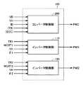
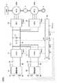
図4は、図1に示したECU100の機能ブロック図である。図4を参照して、ECU100は、コンバータ制御部200と、インバータ制御部110,120とを含む。 FIG. 4 is a functional block diagram of
コンバータ制御部200は、電圧センサ42によって検出された電圧VB、電圧センサ46によって検出された電圧VH、および電流センサ52によって検出された電流IBに基づいて、コンバータ10のスイッチング素子Q1,Q2をオン・オフするためのPWM(Pulse Width Modulation)信号PWCを生成する。
コンバータ制御部200は、さらに、蓄電装置B1の残存容量(State of Charge;充電状態とも呼ばれる)を示す残存容量値SOCを受ける。この値は、たとえば蓄電装置が満充電状態であるときに100%であると定義され、蓄電装置が完全に放電した状態であるときに0%であると定義される。残存容量値SOCは、電圧VB、電流IB、温度TBなどを用いて、種々の公知の手法により算出することができる。
インバータ制御部110は、モータジェネレータMG1のトルク指令値TR1、モータ電流MCRT1およびロータ回転角θ1、ならびに電圧VHに基づいて、インバータ20に含まれるパワートランジスタをオン/オフするためのPWM信号を生成し、その生成したPWM信号を信号PWI1としてインバータ20へ出力する。
インバータ制御部120は、モータジェネレータMG2のトルク指令値TR2、モータ電流MCRT2およびロータ回転角θ2、ならびに電圧VHに基づいて、インバータ22に含まれるパワートランジスタをオン・オフするためのPWM信号を生成し、その生成したPWM信号を信号PWI2としてインバータ22へ出力する。
なお、トルク指令値TR1,TR2は、たとえば、アクセル開度やブレーキ踏込量、車両速度などに基づいて、図示されない車両ECUによって算出される。また、モータ電流MCRT1,MCRT2およびロータ回転角θ1,θ2の各々は、図示されないセンサによって検出される。 Torque command values TR1 and TR2 are calculated by a vehicle ECU (not shown) based on, for example, the accelerator opening, the brake depression amount, the vehicle speed, and the like. Motor currents MCRT1 and MCRT2 and rotor rotation angles θ1 and θ2 are detected by sensors (not shown).
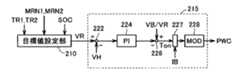
次に、コンバータ10の制御について詳細に説明する。図5は、コンバータ10の制御を説明する機能ブロック図である。図5を参照して、コンバータ制御部200(図3)は、目標値設定部210と、電圧制御部215とを含む。 Next, the control of
目標値設定部210は、モータジェネレータMG1,MG2のトルク(代表的には、トルク指令値TR1,TR2)および回転速度MRN1,MRN2(指令値あるいは、回転角θ1,θ2の検出に基づく検出値)、ならびに蓄電装置B1の残存容量値SOCに基づいて、電圧VHの目標値(目標電圧VR)を生成する。 Target
たとえば、目標値設定部210は、モータジェネレータMG1および/またはMG2の力行動作時および回生制動時においては、モータジェネレータMG1,MG2のトルク指令値TR1,TR2および回転速度MRN1,MRN2に応じて、システム電圧VHが適切なレベルとなるように目標電圧VRを設定する。たとえば、目標値設定部210は、回転速度MRN(MRN1,MRN2を総括的に示すもの、以下同じ)およびトルク指令値TR(TR1,TR2を総括的に示すもの、以下同じ)の組合わせによって示されるモータ動作点毎に目標電圧VRが設定されたマップを参照することによって、目標電圧VRを設定する。これにより、回転速度MRNおよびトルク(トルク指令値TR)に基づいて、モータジェネレータMG1,MG2に応じた適切な目標電圧VRを設定できる。 For example, target
基本的には、モータジェネレータMG(MG1,MG2)を総括的に示すもの、以下同じ)による誘起電圧よりも高い電圧にシステム電圧VHを設定して、モータ電流の制御が可能となるように、目標電圧VRが設定される。また、システム電圧VHに応じて、モータジェネレータMG1,MG2での損失(銅損、鉄損)、インバータ20,22での損失(オン損失、スイッチング損失)、コンバータ10での損失(オン損失、スイッチング損失)、リアクトルL1での損失(銅損、鉄損)等が変化するので、これらの損失特性についても考慮した上で、各モータ動作点でのマップ値(目標電圧VR)を設定することが好ましい。 Basically, the system voltage VH is set to a voltage higher than the induced voltage by the motor generator MG (MG1, MG2), which is generally shown below, so that the motor current can be controlled. A target voltage VR is set. Further, depending on the system voltage VH, losses in motor generators MG1 and MG2 (copper loss, iron loss), losses in
具体的には、モータジェネレータMG1,MG2のそれぞれに対して上述したマップが設定される。また、各モータジェネレータに対応するマップ、および、回転速度MRN1,MRN2およびトルク指令値TR1,TR2に基づいて、モータジェネレータMG1,MG2のそれぞれに対応する目標電圧が求められる。それらの目標電圧の最大値が電源システム全体での目標電圧VRに設定される。 Specifically, the map described above is set for each of motor generators MG1 and MG2. In addition, target voltages corresponding to motor generators MG1 and MG2 are determined based on maps corresponding to the motor generators, rotation speeds MRN1 and MRN2, and torque command values TR1 and TR2. The maximum value of these target voltages is set to the target voltage VR in the entire power supply system.
なお、トルク指令値TR1,TR2の算出は、ユーザによるペダル操作を反映したハイブリッド車両1000全体での要求パワーに基づいて実行される。特に、ハイブリッド自動車では、エンジンの出力パワーとモータジェネレータMG1,MG2の発生パワーとの配分が最適なものとなるように、トルク指令値TR1,TR2が算出される。また、一般的に、トルク指令値TR1,TR2は、蓄電装置B1の入出力可能電力の制限値や、モータジェネレータMG1,MG2あるいはインバータ20,22等の温度上昇度合を反映して、必要に応じて制限される。 The calculation of the torque command values TR1 and TR2 is executed based on the required power in the
再び図5を参照して、電圧制御部215は、減算部222,226と、PI制御部224と、制限部227と、変調部228とを含む。減算部222は、目標電圧VRからシステム電圧VHを減算し、その演算結果をPI制御部224へ出力する。PI制御部224は、目標電圧VRとシステム電圧VHとの偏差を入力として比例積分演算を行ない、その演算結果を減算部226へ出力する。 Referring to FIG. 5 again,
減算部226は、電圧VB/目標電圧VRで示されるコンバータ10の理論昇圧比の逆数からPI制御部224の出力を減算し、その演算結果をデューティ指令Tonとして出力する。
制限部227は、電流IBの方向が負から正に変化したこと(すなわち電流IBがゼロクロスしたこと)を検出すると、一定期間、デューティ指令Tonが示すデューティ比Dの低下を抑制するための制限処理を実行する。なお、上記の一定期間が経過すると、制限部227は、デューティ比Dの低下を抑制する制限処理を解除する。変調部228は、デューティ指令Tonと図示しない発振部により生成される搬送波(キャリア波)とに基づいてPWM信号PWCを生成する。 When the
図5に示した制御構成によって、本実施の形態の電源システムでは、力行動作時には、蓄電装置B1から放電された電力を、負荷装置の入力電圧としてのシステム電圧VHに変換して、電力線(正極ラインPL2)に出力するように電力変換動作が実行される。一方、回生制動動作時には、電力線(正極ラインPL2)上の充電電力により、蓄電装置B1を充電するように電力変換動作が実行される。 With the control configuration shown in FIG. 5, in the power supply system of the present embodiment, during powering operation, the power discharged from the power storage device B1 is converted into the system voltage VH as the input voltage of the load device, and the power line (positive electrode) The power conversion operation is executed so as to output to the line PL2). On the other hand, during the regenerative braking operation, the power conversion operation is performed so as to charge power storage device B1 with the charging power on the power line (positive line PL2).
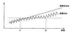
図6は、電流IBが負側から正側に変化する場合の電流IBの波形図である。図6を参照して、電流IBは、周期的に増減を繰返しながら、負側から正側に変化する。たとえばアクセルオフ時には、車両を減速させるためにモータジェネレータMG2が発電する(回生制動を行なう)とともに、生成された電力が蓄電装置B1に蓄えられる。この場合には電流IBは負領域にある。次にユーザがアクセルペダルを踏み込んだ場合(アクセルオン時)にはモータジェネレータMG2から駆動力を発生させるために、蓄電装置B1からモータジェネレータMG2に電力が供給される。したがって電流IBは負から正に変化する。 FIG. 6 is a waveform diagram of the current IB when the current IB changes from the negative side to the positive side. Referring to FIG. 6, current IB changes from the negative side to the positive side while periodically increasing and decreasing. For example, when the accelerator is off, motor generator MG2 generates power (performs regenerative braking) to decelerate the vehicle, and the generated power is stored in power storage device B1. In this case, the current IB is in the negative region. Next, when the user depresses the accelerator pedal (when the accelerator is on), electric power is supplied from power storage device B1 to motor generator MG2 to generate driving force from motor generator MG2. Therefore, the current IB changes from negative to positive.
理想的には、電流IBは直線的に変化し、0である状態が瞬間的にしか発生しない。しかしながら、実際にはデッドタイムの影響によって、電流IBの値が0付近に張り付く現象が発生する。図6は実際の電流IBの変化を模式的に示しているが、たとえば図6に示すように、時刻t1から時刻t2までの期間においては、電流IBの上限ピークが0を上回ることができなかったり、下限ピークが0を下回ることができなかったりする。さらに、電流IBの値がなかなか上昇しなくなる。この結果、理想的な電流IBに比べて実際の電流IBが低くなる。 Ideally, the current IB varies linearly, and a zero state occurs only momentarily. However, in practice, a phenomenon occurs in which the value of the current IB sticks to near 0 due to the influence of the dead time. FIG. 6 schematically shows a change in the actual current IB. However, as shown in FIG. 6, for example, during the period from time t1 to time t2, the upper limit peak of the current IB cannot exceed 0. Or the lower limit peak cannot fall below zero. Furthermore, the value of the current IB does not increase easily. As a result, the actual current IB is lower than the ideal current IB.
このような状態では、理想的な電流IBと実際の電流IBとの差はコンデンサCからの放電電流によって補われる。しかしコンデンサCが放電することによって電圧VHが低下する。このため、次に説明する課題が発生する。 In such a state, the difference between the ideal current IB and the actual current IB is compensated by the discharge current from the capacitor C. However, when the capacitor C is discharged, the voltage VH decreases. For this reason, the subject demonstrated below generate | occur | produces.
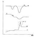
図7は、電圧VHの低下時に生じうる課題を説明するための図である。
図7を参照して、電流IBが0付近で停滞すると電圧VHが目標電圧VRよりも低下する。この場合、電圧制御部215(図5)は、フィードバック制御を実行することにより、電圧VHが上昇するようデューティ指令Tonを生成する。デューティ比Dが低下すれば昇圧比が大きくなるので、電圧VHを上昇させることが可能になる。したがって電圧制御部250はデューティ比Dを低下させるためのデューティ指令Tonを生成する。FIG. 7 is a diagram for explaining a problem that may occur when the voltage VH decreases.
Referring to FIG. 7, when current IB stagnates around 0, voltage VH is lower than target voltage VR. In this case, the voltage control unit 215 (FIG. 5) generates a duty command Ton so that the voltage VH increases by executing feedback control. If the duty ratio D decreases, the step-up ratio increases, so that the voltage VH can be increased. Therefore, the voltage controller 250 generates a duty command Ton for reducing the duty ratio D.
しかしながらデッドタイムの影響により電流IBは0付近で停滞する。上述したように、リアクトルL1がポンプ電流により蓄積された電磁エネルギーを放電電流に重畳することで電圧VHが上昇する。しかしながら電流IBが0付近の状態では、このような作用を発現させることは困難であるので、デューティ比Dを小さくしても昇圧への効果が生じにくい。一方、電圧制御部250は、電圧VHに基づくフィードバック制御を行なっているので、電圧VHが低下するほどデューティ比Dを小さくする。 However, the current IB stagnates around 0 due to the influence of the dead time. As described above, the voltage LH rises when reactor L1 superimposes the electromagnetic energy accumulated by the pump current on the discharge current. However, in the state where the current IB is close to 0, it is difficult to achieve such an effect, so that even if the duty ratio D is reduced, the effect on boosting is unlikely to occur. On the other hand, since voltage control unit 250 performs feedback control based on voltage VH, duty ratio D decreases as voltage VH decreases.
この結果、電流IBが0付近で停滞した状態が終わったときにはデューティ比Dが低すぎることとなる。その一方で、コンバータ10は通常の昇圧動作が可能な状態となる。この結果、電圧VHが目標電圧VRに戻るとともに電流IBが急激に上昇する。したがって破線の丸囲みで示されるような電流IBのサージが発生する。サージ成分が過大になると、コンバータ10への損傷の影響が生じる可能性がある。 As a result, the duty ratio D is too low when the state where the current IB stagnates near 0 ends. On the other hand,
本実施の形態では、以下のようにデューティ比Dを制御することによってサージ電流を抑制する。 In the present embodiment, the surge current is suppressed by controlling the duty ratio D as follows.
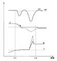
図8は、実施の形態1によるデューティ比Dの制御を説明する図である。図8を参照して、時刻t11において、コンバータ制御部200(図5)は電流IBの0クロスを判定する。電流IBのゼロクロスを判定する方法としては、電流センサ52の検出値を用いる方法を採用できる。ただし、既に説明したように、スイッチング素子Q1,Q2のスイッチング動作に伴って電流IBが周期的に増減するので電流IBも変化する。したがって、たとえば所定周期で電流IBの値をサンプリングする。これにより電流IBの短時間での変動(周期的変動)を抑制できるので、電流IBのゼロクロスを検出できる。 FIG. 8 is a diagram for explaining control of the duty ratio D according to the first embodiment. Referring to FIG. 8, at time t11, converter control unit 200 (FIG. 5) determines zero crossing of current IB. As a method for determining the zero crossing of the current IB, a method using the detection value of the
また、蓄電装置の電流を検出するための方法としては、負荷装置のパワー(モータジェネレータMG1のパワーと損失、モータジェネレータMG2のパワーと損失との合計)を算出し、その算出されたパワーから蓄電装置の電流を算出する方法も採用できる。 As a method for detecting the current of the power storage device, the power of the load device (the sum of the power and loss of the motor generator MG1 and the power and loss of the motor generator MG2) is calculated, and the power is stored from the calculated power. A method for calculating the current of the apparatus can also be adopted.
コンバータ制御部200(より具体的には制限部227)は、電流IBのゼロクロス、(負方向から正方向への電流IBの変化)を検知すると、一定時間、デューティ比Dの下限値が通常時の下限値よりも高くなるようにデューティ指令Tonに対する制限処理を実行する。なお「通常時」とは、負方向から正方向への電流IBの向きの変化が生じない場合を意味する。したがって、通常時とは、電流IBの向きが負方向の場合、正方向の場合、および正方向から負方向に変化する場合を含む。 When converter control unit 200 (more specifically, limiting unit 227) detects a zero cross of current IB (change in current IB from the negative direction to the positive direction), the lower limit value of duty ratio D is normal for a certain period of time. Limit processing for the duty command Ton is executed so as to be higher than the lower limit value. “Normal time” means a case where the direction of the current IB does not change from the negative direction to the positive direction. Therefore, the normal time includes the case where the direction of the current IB is the negative direction, the positive direction, and the case where the current IB changes from the positive direction to the negative direction.
通常時のデューティ比の下限値は、たとえば蓄電装置B1から取り出し可能な電力に基づき定められる。制限処理の実行時におけるデューティ比Dの下限値は特に限定されるものではないが、一つの実施形態を示すと、通常時のデューティ比の下限値の1.2倍の値に設定される。 The lower limit value of the duty ratio at normal time is determined based on, for example, electric power that can be taken out from power storage device B1. The lower limit value of the duty ratio D at the time of executing the limiting process is not particularly limited, but in one embodiment, it is set to a value that is 1.2 times the lower limit value of the normal duty ratio.
また、制限処理を実行する時間は、たとえば電圧VHが低下し始めてから元の値に復帰するまでの期間として、実験、あるいはシミュレーションなどによって求められた値を採用できる。 As the time for executing the limiting process, for example, a value obtained by experiment or simulation can be adopted as a period from when the voltage VH starts to decrease until it returns to the original value.
上記の制限処理を実行することによって、電流IBが0付近に張り付いた状態が終了した直後に電流IBが急上昇するのを抑制できる。したがって電流IBのサージを抑制できる。時刻t12において、制限部227は上記の制限処理を終了させる。これによりデューティ比Dの下限値が通常時の下限値となる。 By executing the above limiting process, it is possible to suppress the current IB from rapidly increasing immediately after the state where the current IB is stuck near 0 is completed. Therefore, the surge of the current IB can be suppressed. At time t12, the
以上のように、実施の形態1によれば、蓄電装置に流れる電流(リアクトルに流れる電流)のゼロクロスを検知すると、一定期間、スイッチング素子Q1,Q2のデューティ比の下限値の低下を制限する。具体的には、蓄電装置に流れる電流が負から正に変化する場合には、蓄電装置に流れる電流の方向が変化しない場合に比較してデューティ比の下限値を高くする。これによって、蓄電装置に流れる電流が負側から正側に増加した場合に、サージ成分が生じることを回避できる。 As described above, according to the first embodiment, when the zero crossing of the current flowing through the power storage device (current flowing through the reactor) is detected, the lowering of the lower limit value of the duty ratio of switching elements Q1, Q2 is limited for a certain period. Specifically, when the current flowing through the power storage device changes from negative to positive, the lower limit value of the duty ratio is set higher than when the direction of the current flowing through the power storage device does not change. Thus, it is possible to avoid the occurrence of a surge component when the current flowing through the power storage device increases from the negative side to the positive side.
[実施の形態2]
実施の形態2に従うハイブリッド車両の構成は図1に示すハイブリッド車両1000の構成と同様であるので以後の説明は繰返さない。実施の形態2におけるコンバータ制御部200の構成は、図5に示す構成と同様である。ただし、スイッチング素子Q1,Q2のデューティ比の下限値の低下を制限する方法において、実施の形態2は実施の形態1と異なる。[Embodiment 2]
Since the configuration of the hybrid vehicle according to the second embodiment is similar to the configuration of
図9は、実施の形態2によるデューティ比Dの制御を説明する図である。図9を参照して、時刻t11において、コンバータ制御部200(図5)は電流IBのゼロクロスを検出する。この検出方法は実施の形態1と同様の方法を適用できる。次にコンバータ制御部200(より具体的には制限部227)は、一定の時間変化率に従ってデューティ比Dを低下させる。この時間変化率は、通常時のデューティ比Dの時間変化率よりも小さい値として定められる。すなわち、電流IBのゼロクロスが検出された場合には、デューティ比Dは通常時に比べて緩やかに低下する。 FIG. 9 is a diagram for explaining control of the duty ratio D according to the second embodiment. Referring to FIG. 9, at time t <b> 11, converter control unit 200 (FIG. 5) detects a zero cross of current IB. As this detection method, the same method as in the first embodiment can be applied. Next, converter control unit 200 (more specifically, limiting unit 227) reduces duty ratio D according to a constant time change rate. This time change rate is determined as a value smaller than the time change rate of the duty ratio D in the normal state. That is, when the zero cross of the current IB is detected, the duty ratio D gradually decreases compared to the normal time.
デューティ比Dの低下率の制限は、一定期間にわたり継続される。この「一定期間」は、実施の形態1と同様に、電圧VHが低下し始めてから元の値に復帰するまでの期間として、実験、シミュレーションなどによって求められた値を採用できる。時刻t12において、制限部227は上記の制限処理を終了させる。これによりデューティ比Dの下限値が通常時の下限値となる。 The limitation on the reduction rate of the duty ratio D is continued for a certain period. As this “fixed period”, as in the first embodiment, a value obtained by experiment, simulation, or the like can be adopted as a period from when the voltage VH starts to decrease until it returns to the original value. At time t12, the
このように実施の形態2ではデューティ比Dの低下率を制限する。これにより電流IBが負から正に変化する場合においてデューティ比Dが下がりすぎるのを抑制できる。したがって、実施の形態1と同様に、蓄電装置に流れる電流が負側から正側に増加した場合に、サージ成分が生じることを回避できる。 As described above, in the second embodiment, the decreasing rate of the duty ratio D is limited. As a result, when the current IB changes from negative to positive, it is possible to suppress the duty ratio D from being lowered excessively. Therefore, as in the first embodiment, it is possible to avoid the occurrence of a surge component when the current flowing through the power storage device increases from the negative side to the positive side.
(電源システムの変形例)
図10は、電源システムの構成の変形例を示す図である。図10を参照して、ハイブリッド車両1000Aは、蓄電装置およびコンバータの組を複数備える点においてハイブリッド車両1000と異なる。すなわち、ハイブリッド車両1000Aは、蓄電装置B2、コンバータ12、電圧センサ44をさらに備える点において、ハイブリッド車両1000Aと異なる。コンバータ12の構成はコンバータ10の構成と同様である。また、蓄電装置B2に対応して電圧センサ44、電流センサ54および温度センサ64が設けられる。(Modification of power supply system)
FIG. 10 is a diagram illustrating a modification of the configuration of the power supply system. Referring to FIG. 10,
蓄電装置B1に対応して設けられた各種センサからは、電圧VB1、温度T1および電流I1の検出値がECU100に送られる。同様に蓄電装置B2に対応して設けられた各種センサからは、電圧VB2、温度T2および電流I2の検出値がECU100に送られる。ECU100は、これらの検出値に基づいて、コンバータ10,12をそれぞれ制御するための信号PWC1,PWC2を生成する。 Detection values of voltage VB1, temperature T1, and current I1 are sent to
ECU100は、たとえば電圧VHが目標電圧VRとなるようにコンバータ10を電圧制御するための信号PWC1を生成してコンバータ10に出力し、蓄電装置B2に流れる電流I2が目標電流となるようにコンバータ12を電流制御するための信号PWC2を生成してコンバータ12に出力する。コンバータ12を電流制御する場合においても、コンバータ12に含まれる2つのスイッチング素子のオン・オフ期間の比(デューティ比)が制御される。したがって、図10に示した構成においても、本発明を適用できる。
なお、蓄電装置および対応のコンバータの組が3以上の複数個並列接続された構成の電源システムにおいても、本発明を適用できることを確認的に記載する。 It should be noted that the present invention can also be applied to a power supply system having a configuration in which three or more sets of power storage devices and corresponding converters are connected in parallel.
また、蓄電装置、コンバータ(電圧変換装置)、および、蓄電装置と電力を授受する負荷を備える車両であれば、本発明を適用できる。したがって、ハイブリッド車両以外にも、電気自動車、燃料電池車等にも本発明を適用できる。また、負荷装置を車両駆動力発生用の電動機(モータジェネレータ)に限定することなく、その他の負荷装置に適用される電源システムについても、蓄電装置およびコンバータ(電力変換装置)を備え、なおかつ負荷装置と蓄電装置との間で電力を授受する構成であれば、本発明の適用が可能である。 Further, the present invention can be applied to any vehicle provided with a power storage device, a converter (voltage conversion device), and a load that exchanges power with the power storage device. Therefore, the present invention can be applied to electric vehicles, fuel cell vehicles, and the like in addition to hybrid vehicles. In addition, the load device is not limited to an electric motor (motor generator) for generating vehicle driving force, and a power supply system applied to other load devices also includes a power storage device and a converter (power converter), and the load device. The present invention can be applied as long as power is transferred between the power storage device and the power storage device.
今回開示された実施の形態はすべての点で例示であって制限的なものではないと考えられるべきである。本発明の範囲は上記した説明ではなくて特許請求の範囲によって示され、特許請求の範囲と均等の意味および範囲内でのすべての変更が含まれることが意図される。 The embodiment disclosed this time should be considered as illustrative in all points and not restrictive. The scope of the present invention is defined by the terms of the claims, rather than the description above, and is intended to include any modifications within the scope and meaning equivalent to the terms of the claims.
2 エンジン、4 動力分割機構、6 車輪、10,12 コンバータ、20,22 インバータ、31,32 駆動回路、42,44,46 電圧センサ、52,54 電流センサ、62,64 温度センサ、100 ECU、110,120 インバータ制御部、200 コンバータ制御部、210 目標値設定部、215 電圧制御部、222,226 減算部、224 PI制御部、227 制限部、228 変調部、1000,1000A ハイブリッド車両、B1,B2 蓄電装置、C コンデンサ、D デューティ比、D1,D2 ダイオード、L1 リアクトル、MG1,MG2 モータジェネレータ、NL 負極ライン、PL1,PL2 正極ライン、Q1,Q2 電力用半導体スイッチング素子。 2 engine, 4 power split mechanism, 6 wheels, 10, 12 converter, 20, 22 inverter, 31, 32 drive circuit, 42, 44, 46 voltage sensor, 52, 54 current sensor, 62, 64 temperature sensor, 100 ECU, 110, 120 Inverter control unit, 200 Converter control unit, 210 Target value setting unit, 215 Voltage control unit, 222, 226 Subtraction unit, 224 PI control unit, 227 Limiting unit, 228 Modulation unit, 1000, 1000A Hybrid vehicle, B1, B2 power storage device, C capacitor, D duty ratio, D1, D2 diode, L1 reactor, MG1, MG2 motor generator, NL negative line, PL1, PL2 positive line, Q1, Q2 Power semiconductor switching element.
Claims (4)
Translated fromJapanese前記正極ラインおよび前記負極ラインに接続されるコンデンサと、
前記負荷装置に対して前記直流電力を入出力する蓄電装置と、
前記正極ラインおよび前記負極ライン間に直列接続された上アーム素子および下アーム素子と、前記上アーム素子および前記下アーム素子の接続点と前記蓄電装置との間の電流経路に介挿接続されるリアクトルとを含み、前記蓄電装置の第1の電圧と前記正極ラインおよび前記負極ライン間の第2の電圧とを相互に変換する電圧変換装置と、
前記上アーム素子および前記下アーム素子が同時にオフするデッドタイムが存在するように前記上アーム素子および前記下アーム素子のスイッチング動作を制御し、かつ前記第2の電圧が目標電圧より低下した場合には、前記上アーム素子のデューティ比を低下させることにより前記第2の電圧を上昇させる制御装置とを備え、
前記制御装置は、前記蓄電装置に流れる電流の向きが、前記電圧変換装置から前記蓄電装置への向きである負方向から前記負方向と逆の正方向に変化した場合には、前記負方向から前記正方向への前記電流の向きの変化が生じない通常時に比較して、前記第2の電圧を上昇させるための前記デューティ比の低下を制限する、電源システム。A positive electrode line and a negative electrode line connected to a load device capable of transmitting and receiving DC power;
A capacitor connected to the positive line and the negative line;
A power storage device that inputs and outputs the DC power to and from the load device;
An upper arm element and a lower arm element connected in series between the positive electrode line and the negative electrode line, and an electric current path between a connection point of the upper arm element and the lower arm element and the power storage device A voltage converter that mutually converts a first voltage of the power storage device and a second voltage between the positive line and the negative line;
When the switching operation of the upper arm element and the lower arm element is controlled so that there is a dead time in which the upper arm element and the lower arm element are simultaneously turned off, and the second voltage is lower than the target voltage Comprises a control device for raising the second voltage by lowering the duty ratio of the upper arm element,
When the direction of the current flowing through the power storage device changes from the negative direction, which is the direction from the voltage conversion device to the power storage device, in the positive direction opposite to the negative direction, the control device starts from the negative direction. The power supply system which restrict | limits the fall of the said duty ratio for raising the said 2nd voltage compared with the normal time when the change of the direction of the said current to the said positive direction does not arise.
前記電源システムと直流電力を授受する負荷装置とを備える、車両。The power supply system according to any one of claims 1 to 3,
A vehicle comprising the power supply system and a load device that exchanges DC power.
Priority Applications (1)
| Application Number | Priority Date | Filing Date | Title |
|---|---|---|---|
| JP2008286849AJP2010115056A (en) | 2008-11-07 | 2008-11-07 | Power supply system and vehicle |
Applications Claiming Priority (1)
| Application Number | Priority Date | Filing Date | Title |
|---|---|---|---|
| JP2008286849AJP2010115056A (en) | 2008-11-07 | 2008-11-07 | Power supply system and vehicle |
Publications (1)
| Publication Number | Publication Date |
|---|---|
| JP2010115056Atrue JP2010115056A (en) | 2010-05-20 |
Family
ID=42303156
Family Applications (1)
| Application Number | Title | Priority Date | Filing Date |
|---|---|---|---|
| JP2008286849AWithdrawnJP2010115056A (en) | 2008-11-07 | 2008-11-07 | Power supply system and vehicle |
Country Status (1)
| Country | Link |
|---|---|
| JP (1) | JP2010115056A (en) |
Cited By (4)
| Publication number | Priority date | Publication date | Assignee | Title |
|---|---|---|---|---|
| US10027234B2 (en) | 2015-07-24 | 2018-07-17 | Mitsubishi Electric Corporation | Power conversion device for performing power conversion between DC and DC by controlling switching of a semiconductor switching element |
| JP2018191435A (en)* | 2017-05-08 | 2018-11-29 | トヨタ自動車株式会社 | Electric power supply for vehicle |
| US11183933B2 (en) | 2019-01-22 | 2021-11-23 | Denso Corporation | Control device for DC-DC converter |
| CN120016658A (en)* | 2025-04-18 | 2025-05-16 | 深圳市德兰明海新能源股份有限公司 | Duty cycle adjustment method and charging device |
- 2008
- 2008-11-07JPJP2008286849Apatent/JP2010115056A/ennot_activeWithdrawn
Cited By (5)
| Publication number | Priority date | Publication date | Assignee | Title |
|---|---|---|---|---|
| US10027234B2 (en) | 2015-07-24 | 2018-07-17 | Mitsubishi Electric Corporation | Power conversion device for performing power conversion between DC and DC by controlling switching of a semiconductor switching element |
| JP2018191435A (en)* | 2017-05-08 | 2018-11-29 | トヨタ自動車株式会社 | Electric power supply for vehicle |
| US11183933B2 (en) | 2019-01-22 | 2021-11-23 | Denso Corporation | Control device for DC-DC converter |
| CN120016658A (en)* | 2025-04-18 | 2025-05-16 | 深圳市德兰明海新能源股份有限公司 | Duty cycle adjustment method and charging device |
| CN120016658B (en)* | 2025-04-18 | 2025-08-05 | 深圳市德兰明海新能源股份有限公司 | Duty cycle adjustment method and charging device |
Similar Documents
| Publication | Publication Date | Title |
|---|---|---|
| JP4179351B2 (en) | Power supply system, vehicle equipped with the same, method for controlling power supply system, and computer-readable recording medium recording a program for causing computer to execute control of power supply system | |
| JP4380772B2 (en) | POWER SUPPLY DEVICE, VEHICLE EQUIPPED WITH THE SAME, CONTROL METHOD FOR POWER SUPPLY DEVICE, AND COMPUTER-READABLE RECORDING MEDIUM CONTAINING PROGRAM FOR CAUSING COMPUTER TO EXECUTE THE CONTROL METHOD | |
| JP6026093B2 (en) | Power system | |
| JP2013207914A (en) | Controller of voltage converter | |
| JP5315915B2 (en) | Power supply system and control method thereof | |
| JP5320988B2 (en) | Power supply system and power balance control method thereof | |
| JP2010104095A (en) | Power supply system, vehicle equipped with the same, and control method of power supply system | |
| CN101485072A (en) | Voltage converter and vehicle having the same | |
| JP4816575B2 (en) | Power supply system, vehicle equipped with the same, control method of power supply system, and computer-readable recording medium recording a program for causing a computer to execute the control method | |
| JP2009159663A (en) | Electric motor drive device, electric vehicle, and control method of electric motor drive device | |
| JP5326905B2 (en) | Power supply system, electric vehicle including the same, and control method of power supply system | |
| JP2017093144A (en) | Power supply | |
| JP4858494B2 (en) | Vehicle power supply apparatus and control method thereof | |
| JP2009296847A (en) | Power supply of vehicle and method of controlling the same | |
| JP2009261201A (en) | Power system and vehicle with the same | |
| CN104067497B (en) | The control device of voltage conversion device | |
| JP2010115056A (en) | Power supply system and vehicle | |
| JP2009284668A (en) | Power supply system and vehicle equipped with the same | |
| JP5949264B2 (en) | POWER SUPPLY DEVICE, VEHICLE EQUIPPED WITH THE SAME, AND METHOD FOR CONTROLLING POWER SUPPLY DEVICE | |
| JP2010074885A (en) | Power supply system and control method therefor | |
| JP5299166B2 (en) | Power supply system, electric vehicle including the same, and control method of power supply system | |
| JP2009060725A (en) | Vehicle and vehicle control method | |
| JP2014155298A (en) | Power supply system, and vehicle mounting the same | |
| JP2010093981A (en) | Power supply system | |
| JP2013169140A (en) | Electrical power system, electric vehicle provided with the same and control method for the same |
Legal Events
| Date | Code | Title | Description |
|---|---|---|---|
| A300 | Withdrawal of application because of no request for examination | Free format text:JAPANESE INTERMEDIATE CODE: A300 Effective date:20120110 |