JP2010113738A - Force imaging input device and system - Google Patents
Force imaging input device and systemDownload PDFInfo
- Publication number
- JP2010113738A JP2010113738AJP2010030213AJP2010030213AJP2010113738AJP 2010113738 AJP2010113738 AJP 2010113738AJP 2010030213 AJP2010030213 AJP 2010030213AJP 2010030213 AJP2010030213 AJP 2010030213AJP 2010113738 AJP2010113738 AJP 2010113738A
- Authority
- JP
- Japan
- Prior art keywords
- layer
- force
- conductive traces
- touch pad
- deformable
- Prior art date
- Legal status (The legal status is an assumption and is not a legal conclusion. Google has not performed a legal analysis and makes no representation as to the accuracy of the status listed.)
- Pending
Links
Images


Classifications
- G—PHYSICS
- G06—COMPUTING OR CALCULATING; COUNTING
- G06F—ELECTRIC DIGITAL DATA PROCESSING
- G06F3/00—Input arrangements for transferring data to be processed into a form capable of being handled by the computer; Output arrangements for transferring data from processing unit to output unit, e.g. interface arrangements
- G06F3/01—Input arrangements or combined input and output arrangements for interaction between user and computer
- G06F3/03—Arrangements for converting the position or the displacement of a member into a coded form
- G06F3/041—Digitisers, e.g. for touch screens or touch pads, characterised by the transducing means
- G06F3/0416—Control or interface arrangements specially adapted for digitisers
- G06F3/04166—Details of scanning methods, e.g. sampling time, grouping of sub areas or time sharing with display driving
- G—PHYSICS
- G06—COMPUTING OR CALCULATING; COUNTING
- G06F—ELECTRIC DIGITAL DATA PROCESSING
- G06F3/00—Input arrangements for transferring data to be processed into a form capable of being handled by the computer; Output arrangements for transferring data from processing unit to output unit, e.g. interface arrangements
- G06F3/01—Input arrangements or combined input and output arrangements for interaction between user and computer
- G06F3/03—Arrangements for converting the position or the displacement of a member into a coded form
- G06F3/041—Digitisers, e.g. for touch screens or touch pads, characterised by the transducing means
- G06F3/044—Digitisers, e.g. for touch screens or touch pads, characterised by the transducing means by capacitive means
- G06F3/0445—Digitisers, e.g. for touch screens or touch pads, characterised by the transducing means by capacitive means using two or more layers of sensing electrodes, e.g. using two layers of electrodes separated by a dielectric layer
- G—PHYSICS
- G06—COMPUTING OR CALCULATING; COUNTING
- G06F—ELECTRIC DIGITAL DATA PROCESSING
- G06F3/00—Input arrangements for transferring data to be processed into a form capable of being handled by the computer; Output arrangements for transferring data from processing unit to output unit, e.g. interface arrangements
- G06F3/01—Input arrangements or combined input and output arrangements for interaction between user and computer
- G06F3/03—Arrangements for converting the position or the displacement of a member into a coded form
- G06F3/041—Digitisers, e.g. for touch screens or touch pads, characterised by the transducing means
- G06F3/044—Digitisers, e.g. for touch screens or touch pads, characterised by the transducing means by capacitive means
- G06F3/0446—Digitisers, e.g. for touch screens or touch pads, characterised by the transducing means by capacitive means using a grid-like structure of electrodes in at least two directions, e.g. using row and column electrodes
- G—PHYSICS
- G06—COMPUTING OR CALCULATING; COUNTING
- G06F—ELECTRIC DIGITAL DATA PROCESSING
- G06F3/00—Input arrangements for transferring data to be processed into a form capable of being handled by the computer; Output arrangements for transferring data from processing unit to output unit, e.g. interface arrangements
- G06F3/01—Input arrangements or combined input and output arrangements for interaction between user and computer
- G06F3/03—Arrangements for converting the position or the displacement of a member into a coded form
- G06F3/041—Digitisers, e.g. for touch screens or touch pads, characterised by the transducing means
- G06F3/044—Digitisers, e.g. for touch screens or touch pads, characterised by the transducing means by capacitive means
- G06F3/0447—Position sensing using the local deformation of sensor cells
- G—PHYSICS
- G06—COMPUTING OR CALCULATING; COUNTING
- G06F—ELECTRIC DIGITAL DATA PROCESSING
- G06F2203/00—Indexing scheme relating to G06F3/00 - G06F3/048
- G06F2203/041—Indexing scheme relating to G06F3/041 - G06F3/045
- G06F2203/04101—2.5D-digitiser, i.e. digitiser detecting the X/Y position of the input means, finger or stylus, also when it does not touch, but is proximate to the digitiser's interaction surface and also measures the distance of the input means within a short range in the Z direction, possibly with a separate measurement setup
- G—PHYSICS
- G06—COMPUTING OR CALCULATING; COUNTING
- G06F—ELECTRIC DIGITAL DATA PROCESSING
- G06F2203/00—Indexing scheme relating to G06F3/00 - G06F3/048
- G06F2203/041—Indexing scheme relating to G06F3/041 - G06F3/045
- G06F2203/04105—Pressure sensors for measuring the pressure or force exerted on the touch surface without providing the touch position
- G—PHYSICS
- G06—COMPUTING OR CALCULATING; COUNTING
- G06F—ELECTRIC DIGITAL DATA PROCESSING
- G06F2203/00—Indexing scheme relating to G06F3/00 - G06F3/048
- G06F2203/041—Indexing scheme relating to G06F3/041 - G06F3/045
- G06F2203/04106—Multi-sensing digitiser, i.e. digitiser using at least two different sensing technologies simultaneously or alternatively, e.g. for detecting pen and finger, for saving power or for improving position detection
- G—PHYSICS
- G06—COMPUTING OR CALCULATING; COUNTING
- G06F—ELECTRIC DIGITAL DATA PROCESSING
- G06F2203/00—Indexing scheme relating to G06F3/00 - G06F3/048
- G06F2203/041—Indexing scheme relating to G06F3/041 - G06F3/045
- G06F2203/04112—Electrode mesh in capacitive digitiser: electrode for touch sensing is formed of a mesh of very fine, normally metallic, interconnected lines that are almost invisible to see. This provides a quite large but transparent electrode surface, without need for ITO or similar transparent conductive material
Landscapes
- Engineering & Computer Science (AREA)
- General Engineering & Computer Science (AREA)
- Theoretical Computer Science (AREA)
- Human Computer Interaction (AREA)
- Physics & Mathematics (AREA)
- General Physics & Mathematics (AREA)
- Position Input By Displaying (AREA)
- Force Measurement Appropriate To Specific Purposes (AREA)
Abstract
Description
Translated fromJapanese本発明は、全般的には電子システム入力デバイスに関し、より具体的には、力イメージングおよび位置−力イメージング相互キャパシタンス・システムに関する。 The present invention relates generally to electronic system input devices, and more specifically to force imaging and position-force imaging mutual capacitance systems.
多数のタッチ・センシング・デバイスが、コンピュータ・システム、携帯情報端末、携帯電話機、ゲーム・システム、音楽システム、その他の類似物(すなわち、電子システム)での使用のために利用可能である。おそらく、最もよく知られているのは抵抗膜位置センサである。これは、長年にわたってキーボードや位置インジケータとして使用されてきた。他のタイプのタッチ・センシング・デバイスには、抵抗タブレットや、面弾性波デバイス、タッチ・センサ、光センサが含まれ、タッチ・センサは抵抗、キャパシタンス、歪みゲージ、電磁センサ、または圧力センサに基づいたものである。圧力感知位置センサは、ポインティング・デバイス(データ入力デバイスまたは書込デバイスではなく)としての使用に関して、歴史的にほとんど利益を提供してこなかった。というのは、これらを動作させるのに必要な圧力が、指とセンサ面との間のスティクション(一種の摩擦)を本来的に生じるからである。そのようなスティクションは、そのようなデバイスが普及するのを大いに妨げてきた。 A number of touch sensing devices are available for use in computer systems, personal digital assistants, cell phones, gaming systems, music systems, and other similar (ie, electronic systems). Perhaps the best known is the resistive film position sensor. It has been used as a keyboard and position indicator for many years. Other types of touch sensing devices include resistive tablets, surface acoustic wave devices, touch sensors, and optical sensors, which are based on resistance, capacitance, strain gauges, electromagnetic sensors, or pressure sensors. It is a thing. Pressure sensitive position sensors have historically offered little benefit for use as a pointing device (not a data input or writing device). This is because the pressure required to operate them inherently creates stiction (a kind of friction) between the finger and the sensor surface. Such stiction has greatly prevented the spread of such devices.
ポータブル・デバイスの増大する人気と、すべての入力機能を単一のフォーム・ファクタに統合することの付随する必要とのゆえに、タッチ・パッドは、現在、最も人気があり広く使用されているタイプの入力デバイスの1つである。操作上、タッチ・パッドは、「抵抗性」または「容量性」のいずれかとして分類することができる。抵抗タッチ・パッドでは、パッドが、薄い金属の導電層と抵抗層によってコーティングされる。パッドに触れると、導電層が、抵抗層を介して接触し、抵抗の変化(通常は電流の変化として測定される)を引き起こし、この抵抗変化が、タッチ・イベントがパッド上のどこで発生したかを識別するのに使用される。容量タッチ・パッドでは、導電トレースの第1組が、第1方向に走り、誘電絶縁物によって導電トレースの第2組から絶縁され、この導電トレースの第2組は、第2方向(一般に第1方向に直交する)に走る。オーバーラップする導電トレースによって形成されるグリッドが、電荷を蓄積できるキャパシタのアレイを作成する。物体が、タッチ・パッドの近くに持ってこられるか、タッチ・パッドと接触する時に、その位置のキャパシタのキャパシタンスが変化する。この変化を使用して、タッチ・イベントの位置を識別することができる。 Due to the increasing popularity of portable devices and the attendant need to integrate all input functions into a single form factor, touch pads are currently the most popular and widely used type of One of the input devices. In operation, touch pads can be classified as either “resistive” or “capacitive”. In a resistive touch pad, the pad is coated with a thin metal conductive layer and a resistive layer. When the pad is touched, the conductive layer contacts through the resistive layer, causing a change in resistance (usually measured as a change in current), and this resistance change is where the touch event occurred on the pad. Used to identify In a capacitive touch pad, a first set of conductive traces runs in a first direction and is insulated from a second set of conductive traces by a dielectric insulator, the second set of conductive traces being in a second direction (generally the first Run perpendicular to the direction). The grid formed by the overlapping conductive traces creates an array of capacitors that can store charge. When an object is brought near or touches the touch pad, the capacitance of the capacitor at that location changes. This change can be used to identify the location of the touch event.
入力デバイスとしてタッチ・パッドを使用することに対する1つの障害は、タッチ・パッドが、一般に圧力情報または力情報を供給しないことである。力情報は、ユーザがデバイスをどのように操作しているかのより確実な表示を入手するのに使用することができる。すなわち、力情報は、関連する電子デバイスにコマンド信号や制御信号を供給するためのもう1つの入力次元として使用することができる。すなわち、タッチ・パッド入力デバイスの一部として力測定システムを提供することが、有益であるはずである。 One obstacle to using the touch pad as an input device is that the touch pad generally does not provide pressure or force information. Force information can be used to obtain a more reliable indication of how the user is operating the device. That is, the force information can be used as another input dimension for supplying command and control signals to the associated electronic device. That is, it would be beneficial to provide a force measurement system as part of a touch pad input device.
一実施態様で、本発明は、ばね膜によって分離された導電トレースの第1組と第2組を含む力感知タッチ・パッドを提供する。力が加えられる時に、ばね膜は、変形し、トレースの2つの組をより近くに移動する。相互キャパシタンスの結果の変化が、加えられた力の位置(タッチ・パッドの面に対する相対的な)と強さすなわち強度を示すイメージを生成するのに使用される。もう1つの実施態様では、本発明は、2組の駆動トレースと、1組の感知トレースと、ばね膜とを含む組み合わされた位置−力感知タッチ・パッドを提供する。動作中に、駆動トレースのうちの1つが、感知トレースの組と組み合わせて使用されて、1つまたは複数の物体がタッチ・パッドに触れる場所のイメージを生成する。駆動トレースの第2組は、感知トレースとばね膜とを組み合わせて使用されて、加えられた力の強さすなわち強度とタッチ・パッドの面に対する相対的なその力の位置のイメージを生成する。本発明による力タッチ・パッドと、位置−力タッチ・パッドとは、ユーザ操作の増加させたアレイの認識を容易にするためにさまざまな電子デバイスに組み込むことができる。 In one embodiment, the present invention provides a force sensitive touch pad that includes a first set and a second set of conductive traces separated by a spring membrane. When a force is applied, the spring membrane deforms and moves the two sets of traces closer together. The resulting change in mutual capacitance is used to generate an image showing the position of the applied force (relative to the surface of the touch pad) and the strength or intensity. In another embodiment, the present invention provides a combined position-force sensitive touch pad that includes two sets of drive traces, a set of sense traces, and a spring membrane. During operation, one of the drive traces is used in combination with a set of sensing traces to generate an image of where one or more objects touch the touch pad. The second set of drive traces is used in combination with a sensing trace and a spring membrane to produce an image of the strength of the applied force, i.e. the strength and position of that force relative to the surface of the touch pad. The force touch pad and position-force touch pad according to the present invention can be incorporated into various electronic devices to facilitate recognition of an increased array of user operations.
もう1つの実施態様では、説明される力感知アーキテクチャを使用して、ユーザがディスプレイ(たとえば、液晶ディスプレイ・ユニット)に働かせる力の量を検出できるディスプレイを実現することができる。本発明のこの実施態様によるディスプレイ・ユニットは、ユーザ入力の増加させたアレイを容易に認識するのに使用することができる。 In another embodiment, the force sensing architecture described can be used to implement a display that allows a user to detect the amount of force exerted on a display (eg, a liquid crystal display unit). The display unit according to this embodiment of the invention can be used to easily recognize an increased array of user input.
次の説明は、当業者が、特許請求された発明を作り、使用することを可能にするために提示され、下で述べる特定の例(パーソナル・コンピュータ・システム用のタッチ・パッド入力デバイス)の文脈で提供される。この特定の例の変形形態は、当業者にすぐに明白になるであろう。したがって、本明細書に添付された特許請求の範囲は、開示される実施形態によって限定されることを意図されているのではなく、本明細書で開示される原理や特徴と一貫する最も広い範囲を与えられなければならない。例として、本発明による力イメージング・システムは、コンピュータ・ワークステーション、携帯電話機、ハンドヘルド・ディジタル・アシスタント、その他のさまざまな機械類やシステム(機械システム、電気システム、電子システム)用のディジタル制御パネルなどのパーソナル・コンピュータ・システム以外の電子デバイスに同等に適用可能である。 The following description is presented to enable those skilled in the art to make and use the claimed invention, and is described below for a specific example (touch pad input device for a personal computer system) described below. Provided in context. Variations on this particular example will be readily apparent to those skilled in the art. Accordingly, the claims appended hereto are not intended to be limited by the disclosed embodiments, but are the broadest scope consistent with the principles and features disclosed herein. Must be given. By way of example, the force imaging system according to the present invention is a computer workstation, mobile phone, handheld digital assistant, digital control panel for various other machinery and systems (mechanical systems, electrical systems, electronic systems), etc. The present invention is equally applicable to electronic devices other than personal computer systems.
図1を参照すると、タッチ・パッド・デバイス100において実施された、本発明による力検出器の全般的概念が示されている。図示のように、力検出器100には、化粧層105と、感知層110(導電経路115と電気コネクタ120を含む)と、誘電ばね層125(空間的にオフセットされて突起した構造体130を含む)と、駆動層135(導電経路140と電気コネクタ145を含む)と、基部または支持体150とが含まれる(コネクタ120、145が、それぞれ層110と135上の導電トレースごとに一意の接続をもたらすことが、当業者によって理解されるであろう)。 Referring to FIG. 1, the general concept of a force detector according to the present invention implemented in a
化粧層105は、環境条件(たとえば、ちりや湿気)からこのシステムの他の要素を保護し、さらに、ユーザがそれを介して検出器100と相互作用する面を提供する。感知層110上の導電経路115は、駆動層135上の導電経路140にオーバーラップするように配置され、これによって、プレート(導電経路115と140)が、感知層基板110、誘電ばね層125、突起した構造体130によって分離されたキャパシタを形成する。誘電ばね層125と突起した構造体130は、一緒に、力が化粧層105に加えられる時に感知層110の導電経路115を駆動層135の導電経路140に非常に近付ける機構を作成する。この分離の変化が、感知層と駆動層の導電経路(115、140)の間の相互キャパシタンスを変化(増加)させる。これは、化粧層105に加えられた力の量、強度、または強さを示す変化である。基部または支持層150は、力検出器100の構造的完全性をもたらす。 The
図2Aを参照すると、力検出器100の断面図が、その荷重をかけられていない状態または「力なし」状態で示されている。この状態では、感知層110と駆動層135との導電経路(115、140)の間の相互キャパシタンスは、定常状態信号または静止キャパシタンス信号(図1のコネクタ120、145を介して測定される)を提供する。図2Bを参照すると、外力200が化粧層105に加えられる時に、誘電ばね層125が変形し、その結果、感知層110が駆動層135のより近くに移動する。これが、感知層と駆動層との間の相互キャパシタンスの変化(増加)すなわち、この2層の間の距離にほぼ単調に関連し、したがって加えられた力200の強度または強さにほぼ単調に関連する変化を与える。より具体的に言うと、動作中に、トレース140(駆動層135上の)が、一時に1つずつ電気的に刺激され、刺激されたトレースとトレース115(感知層110上の)のそれぞれとに関連する相互キャパシタンスが、測定される。このようにして、化粧層105に加えられた力200の強さすなわち強度のイメージを得ることができる。前に注記したように、相互キャパシタンスのこの変化は、適切な回路を介して判定することができる。 Referring to FIG. 2A, a cross-sectional view of the
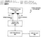
図3を参照すると、力検出器タッチ・パッド100を利用する力イメージング・システム300のブロック図が示されている。図示されているように、力イメージング・システム300には、コネクタ120(感知信号310用)、145(駆動信号315用)を介してタッチ・パッド・コントローラ305に結合された力検出器100が含まれる。タッチ・パッド・コントローラ305は、検出器100に加えられた力の(空間)分布を表す信号をホスト・プロセッサ320に周期的に送る。ホスト・プロセッサ320は、この力情報を解釈して、指定されたコマンド・アクションと制御アクションを実行する(たとえば、ディスプレイ・ユニット325に表示された物体を選択する)ことができる。 Referring to FIG. 3, a block diagram of a
図4を参照すると、動作中に、タッチ・パッド・コントローラ305内の駆動回路400は、駆動信号315とコネクタ145を介して、複数の駆動層導電経路140(図1参照)のそれぞれに順番に電流を送る(「駆動する」)。容量結合のゆえに、この電流の一部は、複数の感知層導電経路115(図1参照)のそれぞれを通って運ばれる。感知回路405(たとえば、電荷増幅器)が、感知信号310から(コネクタ120を介して)アナログ信号を検出し、これらを分析回路410に送る。分析回路410の1つの機能が、検出されたアナログ・キャパシタンス値をディジタル形式に変換する(たとえば、ADコンバータを介して)ことである。分析回路のもう1つの機能は、ホスト・プロセッサ320(図3参照)への送るために、複数のディジタル化されたキャパシタンス値をキュー・アップすることである。分析回路のもう1つの機能は、駆動回路400を制御し、おそらくは、感知回路405の動作を動的に調整する(たとえば、キャパシタンスの「変化」が検出される閾値を変更することによるなど)ことである。本発明での使用に適切なコントローラ305の一実施形態が、その全体を本明細書に組み込まれている、2006年3月15日出願のSteve Hotelling、Christoph Krah、Brian Huppiによる米国特許出願第10/999999号、「Multipoint Touch Screen Controller」に記載されている。 Referring to FIG. 4, during operation, the
もう1つの実施形態では、本発明による力検出器が、容量位置検出器と組み合わされて、位置と力の両方を検出するタッチ・パッド・デバイスが作成される。図5を参照すると、組み合わされた位置−力検出器500には、化粧層505、回路ボードまたは基板510(第1面上の第1の複数の導電駆動経路515と第2面上の複数の感知経路520とを含む)、誘電ばね層525(交番するまたは空間的にオフセットした突起した構造体530を含む)、駆動層535(第2の複数の導電駆動経路を含む)、基部または支持体540が含まれる。一実施形態で、導電駆動経路515、535は、それぞれ基板510上と支持体540上に設けられて、行を形成し、感知導電経路は、基板510上に設けられて、列を形成する。したがって、動作中に、第1駆動経路515が、第1時間期間中に駆動され(一時に1つずつ)、これと同一の時間中に、感知経路520が、1つまたは複数の化粧層タッチの位置を表すイメージを入手するために問い合わされる。同様に、第2駆動経路535が、第2時間期間中に駆動され(一時に1つずつ)、それと同一の時間中に、感知経路520が、やはり、今回は化粧層505に加えられた力の強さすなわち強度を表すイメージを入手するために問い合わされる。相互キャパシタンスの原理に基づくタッチ検出用のコンピュータ入力デバイス(たとえば、タッチ・パッド)の動作は、その全体を組み込まれる、Steve Hotelling、Joshua A. Strickon、Brian Q. Huppiによる米国特許出願第10/840862号、「Multipoint Touchscreen」に記載されている。 In another embodiment, a force detector according to the present invention is combined with a capacitive position detector to create a touch pad device that detects both position and force. Referring to FIG. 5, the combined position-force detector 500 includes a
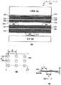
図6を参照すると、本発明のもう1つの実施形態による位置−力タッチ・パッド600が断面図で示されている。この実施形態では、化粧層605に、ポリエステルまたはポリカーボネート薄膜が含まれる。層610には、アクリルベースの感圧接着剤または紫外光硬化接着剤が含まれる。層615は、「上」面に(すなわち、化粧層605に向かって)第1方向に向けられた第1の複数の導電駆動トレース620と、「下」面に第2方向に向けられた複数の導電感知トレース625とを有する両面回路ボードとして機能する。一実施形態で、回路基板層615には、ポリエチレン・テレフタレート(「PET」)などの低温プラスチックまたは熱可塑性樹脂が含まれる。この実施形態では、駆動トレース620と感知トレース625に、プリントされた銀インクを含めることができる。もう1つの実施形態では、回路基板層615に、フレキシブル回路ボードまたはファイバグラスもしくはガラスが含まれ、駆動トレースと感知トレース(620、625)に、インジウム酸化スズ(「ITO」)または銅が含まれる。層630には、一実施形態で、接着剤−PETー接着剤からなる層状組合せが含まれ、ここで、接着剤構成要素は、上で層610に関して説明したものである。層635、640、645には、変化する厚さのPETが含まれる。図示されているように、層640の「下」面は、その上に、第1導電駆動トレース620と実質的に同一方位に向けられた第2の複数の導電駆動トレース650が固定されている。突起し、空間的にオフセットした支持構造体655と層660にも、接着剤−PET−接着剤(層630に似る、上を参照されたい)からなる層状組合せが含まれる。層605〜660は、基部またはスチフナ・プレート665に固定され、これによって支持される。たとえば、ポータブル・コンピュータ・システムまたはノートブック・コンピュータ・システムでは、基部665を、そのコンピュータ・システムのフレームの一部である金属スタンピングなどの堅い材料から形成することができる。同様に、基部665を、携帯情報端末や携帯電話機内の内部フレーミングとすることができる。表1は、タッチ・パッド600の一実施形態の層600〜660のそれぞれの厚さを識別する表である。 Referring to FIG. 6, a position-

動作中に、タッチ・パッド600は、化粧層605が1つまたは複数の位置で触れられることに起因するキャパシタンスの変化(たとえば、減少)を、駆動トレース620と感知トレース625との間の相互キャパシタンスを介して測定する。上で説明した形で、タッチ・パッド600は、感知トレース625と駆動トレース650がより近くに近接するようにされる時に、これらの間の相互キャパシタンスの測定された変化(たとえば、増加)を介して、化粧層に加えられる力をも測定する。この実施形態では、突起した構造体655は、駆動トレースの第2層(650)の両側で使用されて、追加の移動検出能力を与える。 During operation, the
測定動作中に、駆動トレース620のそれぞれが順番に刺激され、それと同時に、駆動トレース620と感知トレース625との間の相互キャパシタンスの変化が測定される。駆動トレース620のそれぞれが刺激され(かつ、キャパシタンスの対応する変化が感知トレース625を介して測定され)たならば、駆動トレース650のそれぞれが、順番に駆動され、感知トレース625が、力に関連する相互キャパシタンスの変化(すなわち、加えられた力に起因するトレース625と650との間の相互キャパシタンス変化)を判定するのに使用される。この形で、化粧層605への「タッチ」入力と「力」入力との両方のイメージを入手することができる。 During the measurement operation, each of the drive traces 620 is stimulated in turn, and at the same time the change in mutual capacitance between the
当業者は、上で説明した「スキャン」シーケンスが必要ではないことを認めるであろう。たとえば、駆動トレース620、650を、オーバーラップする形で刺激することができ、駆動トレース620内の第1トレースを刺激し、これに駆動トレース650内の第1トレースを続け、これに駆動トレース620内の第2トレースを続けるなどとすることができる。その代わりに、駆動トレース620内のトレースのグループをまず刺激し、これに駆動トレース650内のトレースのグループを続けるなどとすることができる。 Those skilled in the art will appreciate that the “scan” sequence described above is not necessary. For example, the drive traces 620, 650 can be stimulated in an overlapping manner, stimulating the first trace in the
一実施形態で、駆動トレース620(タッチ位置測定動作に関連する)は、駆動トレース650(力測定動作に関連する)と感知トレース625(位置測定動作と力測定動作との両方の間に使用される)と異なる幾何形状を使用する。図7を参照すると、駆動トレース620が、内部浮動プレート構造体700を使用し、さらに、感知トレース625と駆動トレース650(この両方が、図示の実施形態では同一の物理的サイズ/構造を有する)に使用される導電トレースのいずれよりも物理的に大きい導電トレースを利用することがわかる。この構成が、1つまたは複数の物体(たとえば、指またはスタイラス)が化粧面605に接触しまたは非常に近接する場所を判定するための感度を高くすることがわかっている。 In one embodiment, drive trace 620 (associated with touch position measurement operation) is used between drive trace 650 (associated with force measurement operation) and sense trace 625 (both position measurement operation and force measurement operation). Use a different geometry. Referring to FIG. 7, the
図8Aを参照すると、本発明による組み合わされたタッチ−力感知タッチ・パッドのもう1つの実施形態(タッチ・パッド800)では、突起した構造体655を、ビードまたはポリマ・ドット805(ゴム・ドットまたはエラストマ・ドットとも称する)に置換することができる。この実施形態では、ビード805は、突起した構造体655(図6参照)に似た形で動作する。図示されているように、ビード805は、薄い接着剤層810の上に乗り、加えられる力が存在しない時に層630、640を指定された距離に保つサイズにされている。ビード805の1つの例示的なレイアウトと間隔を、図8B(平面図)と8C(断面)に示す。表2は、前に図示されたタッチ・パッド600と異なる、タッチ・パッド800の各構成要素の近似寸法を識別する表である。 Referring to FIG. 8A, in another embodiment of the combined touch-force sensitive touch pad according to the present invention (touch pad 800), the protruding
図9Aを参照すると、本発明による組み合わされたタッチ−力感知タッチ・パッドのもう1つの実施形態(タッチ・パッド900)では、変形可能なビードまたはエラストマ・ドット905の単一の層が使用される。タッチ・パッド900では、薄い接着剤層910が、ビードをタッチ・パッド構造の残りに機械的に結合し、この構造自体を基部665に機械的に結合するのに使用される。変形可能なビード905の1つの例示的なレイアウトと間隔を、図9B(平面図)と9C(断面)に示す。表3は、前に図示されたタッチ・パッド600と異なる、タッチ・パッド900の各構成要素の近似寸法を識別する表である。 Referring to FIG. 9A, in another embodiment of the combined touch-force sensitive touch pad according to the present invention (touch pad 900), a single layer of deformable bead or
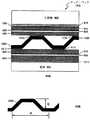
図10Aを参照すると、本発明による組み合わされたタッチ−力感知タッチ・パッドのもう1つの実施形態(タッチ・パッド1000)では、ばね膜1005が、突起した構造体(たとえば、530、655)または変形可能なビード(たとえば、805、905)の代わりに使用される。タッチ・パッド1000では、薄い接着剤層1010が、PETばね1005を層635、640に機械的に結合すると同時に、層645を基部665に機械的に結合するのに使用される。図10Bを参照すると、一実施形態で、ばね膜には、距離対高さ比(すなわち、a/b)が通常は約10:1から50:1までの範囲内にあるPETの単一の波状シートが含まれる。当業者は、任意の所与の実施形態で使用される正確な値が、たとえばタッチ・パッド面の物理的サイズ、全たわみについて指定される重さの量(たとえば、200グラム)、ユーザに提示される「剛性」の所望の感覚などのさまざまな要因に起因して変化する場合があることを認めるであろう。表4は、前に図示されたタッチ・パッド600と異なる、タッチ・パッド1000の各構成要素の近似寸法を識別する表である。 Referring to FIG. 10A, in another embodiment of a combined touch-force sensitive touch pad according to the present invention (touch pad 1000), the
図11Aを参照すると、もう1つの実施形態で、波状ばね膜1005を、くぼみ付きばね膜1105に置換することができる。この実施形態では、ばね膜1105は、たとえば熱成形技法または真空成形技法によって、その中にくぼみを形成された変形可能な材料(たとえば、PET)の単一のシートである。図11B、11Cに、2つの可能なくぼみ配置の上面図を示す。くぼみ付き膜1105の2つの例示的なレイアウト(上面図)が、図11B、11Cに示されている。図11A〜11Cで使用されている「+」記号は、突起した領域を表し、「−」記号は、押し下げられた領域を表す。表5は、図11Aで指定された近似寸法「a」から「e」を識別する表である。 Referring to FIG. 11A, in another embodiment, the undulating
材料、構成要素、回路要素のさまざまな変更が、添付の特許請求の範囲から逸脱せずに可能である。たとえば、図1〜10による駆動トレースおよび感知トレースを、直交するものとして説明した。しかし、駆動トレースが、感知トレースを横切るかこれと交差する形は、一般に、使用される座標系に依存する。たとえば、デカルト座標系では、感知トレースは、駆動トレースに直交であり、これによって、別個のx座標とy座標を有するノードが形成される。その代わりに、極座標系では、感知トレースを同心円とすることができ、駆動トレースを放射状に延びる線とすることができる(またはその逆)。 Various modifications of materials, components, and circuit elements are possible without departing from the scope of the appended claims. For example, the drive and sense traces according to FIGS. 1-10 have been described as being orthogonal. However, the manner in which the drive trace crosses or intersects the sensing trace generally depends on the coordinate system used. For example, in a Cartesian coordinate system, the sense trace is orthogonal to the drive trace, thereby forming a node with separate x and y coordinates. Instead, in the polar coordinate system, the sensing traces can be concentric circles and the drive traces can be radially extending lines (or vice versa).
さらに、図1、2の実施形態では、駆動層135と駆動トレース140(および、したがって、コネクタ145)を、ばね膜125内とばね膜125上に組み込むことができる。すなわち、駆動トレース140を、柔軟な膜125の面に敷設するかエッチングすることができる。同様に、駆動トレース535を、柔軟な膜525(図5参照)に組み込み、その一部とすることができる。 Further, in the embodiment of FIGS. 1 and 2, the
当業者は、図8、9によるビード(図8および9参照)を、突起した構造体130、530、、655(図1、2A、2B、5、、6参照)の代わりに使用することもできることをも認めるであろう。同様に、ばね機構1005(図10参照)、1105(図11参照)を、ビード805(図8参照)、変形可能なビード805、905(図8、9参照)、または突起した構造体130、530、、655(図1、5、、6参照)の代わりに使用することができる。 A person skilled in the art may also use the beads according to FIGS. 8 and 9 (see FIGS. 8 and 9) instead of the protruding
図12Aを参照すると、もう1つの実施形態で、本発明による力検出を、タッチパッドではなくディスプレイ・ユニットに組み込むことができる。たとえば、システム1200には、プロセッサ1205、標準的な入出力(「I/O」)デバイス1210(たとえば、キーボード、マウス、タッチ・パッド、ジョイ・スティック、音声入力)、本発明による力検出能力を組み込んだディスプレイ1215が含まれる。図12Bを参照すると、この実施形態では、ディスプレイ1215に、ディスプレイ要素1220、ディスプレイ要素エレクトロニクス1225、力要素1230、力エレクトロニクス1235が含まれる。この形で、ユーザ1240は、力要素1230を通じてディスプレイ1200のディスプレイ要素1220を見る。一例として、ディスプレイ要素1220とエレクトロニクス1225に、普通の液晶ディスプレイ(「LCD」)ディスプレイを含めることができる。力要素1230に、力のみのセンサ(たとえば、図1および2の実施形態に似た)または力と位置センサ(たとえば、図5〜11の実施形態に似た)を含めることができる。力エレクトロニクス1235に、図4で説明した処理回路を含めることができる。すなわち、力エレクトロニクス1235は、本発明によるタッチ・パッドに関して説明したように、相互キャパシタンス信号を駆動し、感知することができる。 Referring to FIG. 12A, in another embodiment, force detection according to the present invention can be incorporated into a display unit rather than a touchpad. For example,
当業者は、説明された力検出テクノロジの使用が、ディスプレイ1215に適用される時に、ITO(すなわち、不透明な銅ではなく)によって得られるものなどの透明なまたは実質的に透明な駆動トレースと感知トレースを利用しなければならないことを認めるであろう。同様に、加えられる力を検出するのに使用されるトレースの第1層(たとえば、駆動トレース)とトレースの第2層(たとえば、感知トレース)との間のギャップ(上の議論を参照されたい)は、透明または実質的に透明でなければならない。たとえば、圧縮可能な透明スペーサを使用して、オフセットした突起した構造体130、支持構造体655、変形可能なビード805、905、またはばね膜1005、1105を実施することができる。 Those skilled in the art will recognize that transparent or substantially transparent drive traces and sensing, such as those obtained with ITO (ie, not opaque copper), when the use of the described force sensing technology is applied to display 1215 I will admit that I have to use trace. Similarly, the gap between the first layer of trace (eg, drive trace) and the second layer of trace (eg, sense trace) used to detect the applied force (see discussion above). ) Must be transparent or substantially transparent. For example, an offset protruding
本願において開示される実施形態のうち、代表的なものの概要を簡単に説明すれば、次のとおりである。
(1)第1面上で第1方向に向けられた第1の複数の導電トレースを有する第1層と、
第1面上で第2方向に向けられた第2の複数の導電トレースを有する第2層と、
前記第1層と前記第2層との間に並置された変形可能な誘電体膜と
を含み、前記第1と第2の複数の導電トレースが、力が前記第1層に加えられる時にキャパシタンス・イメージを作成するように適合され、前記キャパシタンス・イメージが、前記加えられた力の強さを示す
力イメージング・タッチ・パッド。
(2)前記第1の複数の導電トレースと前記第2の複数の導電トレースが、実質的に直交する上記(1)に記載の力イメージング・タッチ・パッド。
(3)前記変形可能な誘電体膜が、
前記第1層に向かって向けられた第1面と前記第2層に向かって向けられた第2面を有する実質的に平坦な膜と、
前記実質的に平坦な膜の前記第1面に結合された第1の複数の突起した構造体と、
前記実質的に平坦な膜の前記第2面に結合された第2の複数の突起した構造体であって、前記第1の複数の突起した構造体から実質的にオフセットされている、前記第2の複数の突起した構造体と
を含む上記(1)に記載の力イメージング・タッチ・パッド。
(4)前記変形可能な誘電体膜が、
実質的に平坦な膜と、
前記実質的に平坦な膜の1面に固定された複数の変形可能ビードであって、力が前記第2層に向かって前記第1層に加えられる時に圧縮されるように適合される、前記複数の変形可能ビードと
を含む上記(1)に記載の力イメージング・タッチ・パッド。
(5)前記変形可能な誘電体膜が、1つまたは複数の熱可塑性ばねを含む上記(1)に記載の力イメージング・タッチ・パッド。
(6)前記変形可能な誘電体膜が、くぼみ付き変形可能膜を含む上記(1)に記載の力イメージング・タッチ・パッド。
(7)前記熱可塑性ばねが、ポリエチレン・テレフタレートからなる上記(5)に記載の力イメージング・タッチ・パッド。
(8)前記第1と第2の複数の導電トレースに電気的に結合された相互キャパシタンス測定回路をさらに含む上記(1)に記載の力イメージング・タッチ・パッド。
(9)第1面上で第1方向に向けられた第1の複数の導電トレースと第2面上で第2方向に向けられた第2の複数の導電トレースを有する第1層と、
実質的に前記第1方向に向けられた第3の複数の導電トレースを有する第2層と、
基部層と、
前記第1層と前記第2層との間に並置された第1変形可能膜と、
前記第2層と前記基部層との間に並置された第2変形可能膜と
を含み、前記第1と第2の複数の導電トレースが、1つまたは複数の物体が前記第1面に非常に近接するようになる時に第1キャパシタンス・イメージを作成するように適合され、前記第1キャパシタンス・イメージが、前記1つまたは複数の物体が前記第1面に対して相対的にどこに置かれているかを示し、
前記第2と第3の複数の導電トレースが、力が前記第1層に加えられる時に第2キャパシタンス・イメージを作成するように適合され、前記第2キャパシタンス・イメージが、前記加えられた力の強さを示す
力と位置イメージング・タッチ・パッド。
(10)前記第1層が、フレキシブル回路ボードを含む上記(9)に記載の力と位置イメージング・タッチ・パッド。
(11)前記第1層が、熱可塑性樹脂の1つまたは複数の層を含む上記(9)に記載の力と位置イメージング・タッチ・パッド。
(12)前記第1の複数の導電トレースと前記第2の複数の導電トレースが、実質的に直交する上記(9)に記載の力と位置イメージング・タッチ・パッド。
(13)前記第2層が、フレキシブル回路ボードを含む上記(9)に記載の力と位置イメージング・タッチ・パッド。
(14)前記第2層が、熱可塑性樹脂の1つまたは複数の層を含む上記(9)に記載の力と位置イメージング・タッチ・パッド。
(15)前記第1変形可能膜が第1の複数の突起した構造体を含み、前記第2変形可能膜が第2の複数の突起した構造体を含み、前記第1と第2の突起した構造体が、互いから実質的に空間的にオフセットされている上記(9)に記載の力と位置イメージング・タッチ・パッド。
(16)前記第1と第2の複数の突起した構造体が熱可塑性樹脂を含む上記(15)に記載の力と位置イメージング・タッチ・パッド。
(17)前記第1変形可能膜が第1の複数の変形可能ビードを含み、前記第2変形可能膜が第2の複数の変形可能ビードを含み、前記第1と第2の複数の変形可能ビードが互いから実質的に空間的にオフセットされている上記(9)に記載の力と位置イメージング・タッチ・パッド。
(18)前記変形可能ビードがエラストマ・ビードを含む上記(17)に記載の力と位置イメージング・タッチ・パッド。
(19)前記第1と第2の複数の突起した構造体のそれぞれが1つまたは複数の熱可塑性ばねを含む上記(9)に記載の力と位置イメージング・タッチ・パッド。
(20)前記熱可塑性ばねがポリエチレン・テレフタレートからなる上記(19)に記載の力と位置イメージング・タッチ・パッド。
(21)前記第1、第2、第3の複数の導電トレースに電気的に結合された相互キャパシタンス測定回路をさらに含む上記(9)に記載の力と位置イメージング・タッチ・パッド。
(22)第1方向に向けられた第1の複数の導電トレースを有する第1面と、
第2方向に向けられた第2の複数の導電トレースを有する第2面であって、前記第1と第2面が、互いに並置され、互いから電気的に絶縁される、前記第2面と、
実質的に前記第1方向に向けられた第3の複数の導電トレースを有する第3面と、
前記第2層と前記第3層との間の変形可能な膜と
を含み、前記第1と第2の複数の導電トレースが、1つまたは複数の物体が前記第1面に非常に近接する時に第1キャパシタンス・イメージを作成するように適合され、前記第1キャパシタンス・イメージが、前記1つまたは複数の物体が前記第1面に対して相対的にどこに置かれているかを示し、
前記第2と第3の複数の導電トレースが、力が前記第1面に加えられる時に第2キャパシタンス・イメージを作成するように適合され、前記第2キャパシタンス・イメージが、前記加えられた力の強さを示す
力と位置イメージング・タッチ・パッド。
(23)前記第1と第2面が、共通の層の面である上記(22)に記載の力と位置イメージング・タッチ・パッド。
(24)前記共通の層が、フレキシブル回路ボードを含む上記(23)に記載の力と位置イメージング・タッチ・パッド。
(25)前記共通の層が、熱可塑性樹脂の1つまたは複数の層を含む上記(23)に記載の力と位置イメージング・タッチ・パッド。
(26)前記第1の複数の導電トレースと前記第2の複数の導電トレースが実質的に直交する上記(22)に記載の力と位置イメージング・タッチ・パッド。
(27)前記第3面が、熱可塑性樹脂を含む上記(22)に記載の力と位置イメージング・タッチ・パッド。
(28)前記変形可能な膜が、
前記第1の複数の導電トレースに向かって向けられた第1面と前記第3の複数の導電トレースに向かって向けられた第2面とを有する実質的に平坦な膜と、
前記実質的に平坦な膜の前記第1面に結合された第1の複数の突起した構造体と、
前記実質的に平坦な膜の前記第2面に結合された第2の複数の突起した構造体であって、前記第1の複数の突起した構造体から実質的に空間的にオフセットされている、前記第2の複数の突起した構造体と
を含む上記(22)に記載の力と位置イメージング・タッチ・パッド。
(29)前記変形可能な膜が、
実質的に平坦な膜と、
前記実質的に平坦な膜の1面に固定された複数の変形可能ビードであって、力が前記第2層に向かって前記第1層に加えられる時に圧縮されるように適合される、前記複数の変形可能ビードと
を含む上記(22)に記載の力と位置イメージング・タッチ・パッド。
(30)前記変形可能な膜がくぼみ付き変形可能膜を含む上記(22)に記載の力と位置イメージング・タッチ・パッド。
(31)前記変形可能ビードがポリマを含む上記(29)に記載の力と位置イメージング・タッチ・パッド。
(32)前記変形可能な膜が1つまたは複数の熱可塑性ばねを含む上記(22)に記載の力と位置イメージング・タッチ・パッド。
(33)前記熱可塑性樹脂がポリエチレン・テレフタレートからなる上記(32)に記載の力と位置イメージング・タッチ・パッド。
(34)前記第1、第2、第3の複数の導電トレースに電気的に結合された相互キャパシタンス測定回路をさらに含む上記(22)に記載の力と位置イメージング・タッチ・パッド。
(35)処理ユニットと、
前記処理ユニットに機能的に結合されたディスプレイ・ユニットと、
前記処理ユニットに機能的に結合された相互キャパシタンス測定回路と、
上記(9)と(22)のうちの一項に記載の、前記相互キャパシタンス測定回路に機能的に結合された力と位置イメージング・タッチ・パッドと
を含む電子デバイス。
(36)前記電子デバイスがコンピュータ・システムからなる上記(35)に記載の電子デバイス。
(37)前記電子デバイスが携帯電話機からなる上記(35)に記載の電子デバイス。
(38)前記電子デバイスが、携帯情報端末からなる上記(35)に記載の電子デバイス。
(39)第1面上で第1方向に向けられた第1の複数の導電トレースを有する第1層と、
第1面と第2面を有する変形可能な誘電体膜であって、前記第1面が、前記第1層に並置され、前記第2面が、第2方向に向けられた第2の複数の導電トレースを有する、前記変形可能な誘電体膜と
を含み、前記第1と第2の複数の導電トレースが、力が前記第1層に加えられる時にキャパシタンス・イメージを作成するように適合され、前記キャパシタンス・イメージが、前記加えられた力の強さを示す
力イメージング・タッチ・パッド。
(40)前記第1の複数の導電トレースと前記第2の複数の導電トレースが実質的に直交する上記(39)に記載の力イメージング・タッチ・パッド。
(41)前記変形可能な誘電体膜が、
前記第1と第2面を有する実質的に平坦な膜と、
前記実質的に平坦な膜の前記第1面に結合された第1の複数の突起した構造体と、
前記実質的に平坦な膜の前記第2面に結合された第2の複数の突起した構造体であって、前記第1の複数の突起した構造体から実質的にオフセットされている、前記第2の複数の突起した構造体と
を含む上記(39)に記載の力イメージング・タッチ・パッド。
(42)前記変形可能な誘電体膜が、
前記第1と第2面を有する実質的に平坦な膜と、
前記実質的に平坦な膜の1面に固定された複数の変形可能ビードであって、力が前記第2層に向かって前記第1層に加えられる時に圧縮されるように適合される、前記複数の変形可能ビードと
を含む上記(39)に記載の力イメージング・タッチ・パッド。
(43)前記第1と第2の複数の導電トレースに電気的に結合された相互キャパシタンス測定回路をさらに含む上記(39)に記載の力イメージング・タッチ・パッド。
(44)前記第1層の第2面上の第3の複数の導電トレースをさらに含み、前記変形可能な誘電体膜が、前記第1の複数の導電トレースよりも前記第3の複数の導電トレースの近くに並置され、前記第3の複数の導電トレースが第3方向に向けられ、さらに、前記第1と第3の複数の導電トレースが、物体が前記第1層に接触するようにされる時に、キャパシタンス・イメージを作成するように適合され、前記キャパシタンス・イメージが、前記第1層の前記第1面に対する相対的な、前記物体が前記第1面に接触する位置を示す上記(39)に記載の力イメージング・タッチ・パッド。
(45)前記第1と第3方位が実質的に同一であり、前記第2方位がこれらに対して実質的に直交である上記(44)に記載の力イメージング・タッチ・パッド。
(46)第1面上で第1方向に向けられた第1の複数の導電トレースと第2面上で第2方向に向けられた第2の複数の導電トレースを有する第1層と、
第1面と第2面を有する変形可能な誘電体膜であって、前記第1面が前記第1層に並置され、前記第2面が実質的に前記第1方向に向けられた第3の複数の導電トレースを有する、前記変形可能な誘電体膜と、
前記変形可能な誘電体膜の前記第2面に並置された基部層と
を含み、前記第1と第2の複数の導電トレースが、1つまたは複数の物体が前記第1面に非常に近接するようにされる時に、第1キャパシタンス・イメージを作成するように適合され、前記第1キャパシタンス・イメージが、前記1つまたは複数の物体が前記第1面に対して相対的にどこに置かれるかを示し、
前記第2と第3の複数の導電トレースが、力が前記第1層に加えられる時に、第2キャパシタンス・イメージを作成するように適合され、前記第2キャパシタンス・イメージが前記加えられた力の強さを示す
力と位置イメージング・タッチ・パッド。
(47)前記第1層がフレキシブル回路ボードを含む上記(46)に記載の力と位置イメージング・タッチ・パッド。
(48)前記第1層が熱可塑性樹脂の1つまたは複数の層を含む上記(46)に記載の力と位置イメージング・タッチ・パッド。
(49)前記第1の複数の導電トレースと前記第2の複数の導電トレースが実質的に直交する上記(46)に記載の力と位置イメージング・タッチ・パッド。
(50)前記第2層がフレキシブル回路ボードを含む上記(46)に記載の力と位置イメージング・タッチ・パッド。
(51)前記第2層が熱可塑性樹脂の1つまたは複数の層を含む上記(46)に記載の力と位置イメージング・タッチ・パッド。
(52)前記変形可能な膜が、前記変形可能な膜の前記第1面に並置された第1の複数の突起した構造体と、前記変形可能な膜の前記第2面に並置された第2の複数の突起した構造体とを含み、前記第1と第2の複数の突起した構造体が、互いから実質的に空間的にオフセットされている上記(46)に記載の力と位置イメージング・タッチ・パッド。
(53)前記第1と第2の複数の突起した構造体が、熱可塑性樹脂を含む上記(52)に記載の力と位置イメージング・タッチ・パッド。
(54)前記変形可能な膜が、さらに、第1の複数の変形可能ビードを含む上記(46)に記載の力と位置イメージング・タッチ・パッド。
(55)前記変形可能ビードがエラストマ・ビードを含む上記(54)に記載の力と位置イメージング・タッチ・パッド。
(56)前記第1、第2、第3の複数の導電トレースに電気的に結合された相互キャパシタンス測定回路をさらに含む上記(46)に記載の力と位置イメージング・タッチ・パッド。
(57)ディスプレイ要素と、
その第1面上で第1方向に向けられた第1の複数の実質的に透明の導電トレースを有する第1層であって、前記ディスプレイ要素の第1面に隣接する、前記第1層と、
その第1面上で第2方向に向けられた第2の複数の実質的に透明の導電トレースを有する第2層であって、前記第1層が、前記第2層と前記ディスプレイ要素との間に並置される、前記第2層と、
前記第1層と前記第2層との間に並置された、変形可能な実質的に透明の誘電体膜と
を含み、前記第1と第2の複数の導電トレースが、力が前記第2層に加えられる時にキャパシタンス・イメージを作成するように適合され、前記キャパシタンス・イメージが前記加えられた力の強さを示す
力イメージング・ディスプレイ。
(58)前記ディスプレイ要素が、液晶ディスプレイ要素を含む上記(57)に記載の力イメージング・ディスプレイ。
(59)前記第1と第2層が、インジウム酸化スズ・トレースを含む上記(57)に記載の力イメージング・ディスプレイ。
(60)前記第1の複数の実質的に透明の導電トレースと前記第2の複数の実質的に透明の導電トレースが実質的に直交する上記(57)に記載の力イメージング・ディスプレイ。
(61)前記実質的に透明の変形可能な誘電体膜が、
前記第1層に向かって向けられた第1面と前記第2層に向かって向けられた第2面を有する実質的に平坦な膜と、
前記実質的に平坦な膜の前記第1面に結合された第1の複数の突起した構造体と、
前記実質的に平坦な膜の前記第2面に結合された第2の複数の突起した構造体であって、前記第1の複数の突起した構造体から実質的にオフセットされている、前記第2の複数の突起した構造体と
を含む上記(57)に記載の力イメージング・ディスプレイ。
(62)前記実質的に透明の変形可能な誘電体膜が、
実質的に平坦な膜と、
前記実質的に平坦な膜の1面に固定された複数の変形可能ビードであって、前記変形可能ビードが、力が前記第2層に向かって前記第1層に加えられる時に圧縮されるように適合される、前記複数の変形可能ビードと
を含む上記(57)に記載の力イメージング・ディスプレイ。Of the embodiments disclosed in the present application, the outline of typical ones will be briefly described as follows.
(1) a first layer having a first plurality of conductive traces oriented in a first direction on a first surface;
A second layer having a second plurality of conductive traces oriented in a second direction on the first surface;
A deformable dielectric film juxtaposed between the first layer and the second layer, wherein the first and second plurality of conductive traces have a capacitance when a force is applied to the first layer. A force imaging touch pad adapted to create an image, wherein the capacitance image indicates the strength of the applied force.
(2) The force imaging touch pad according to (1), wherein the first plurality of conductive traces and the second plurality of conductive traces are substantially orthogonal to each other.
(3) The deformable dielectric film is
A substantially flat film having a first surface directed toward the first layer and a second surface directed toward the second layer;
A first plurality of protruding structures coupled to the first surface of the substantially flat film;
A second plurality of projecting structures coupled to the second surface of the substantially flat film, the first plurality of projecting structures being substantially offset from the first plurality of projecting structures; The force imaging touch pad according to (1), comprising two or more protruding structures.
(4) The deformable dielectric film is
A substantially flat film,
A plurality of deformable beads secured to one side of the substantially flat membrane, adapted to be compressed when a force is applied to the first layer toward the second layer; The force imaging touch pad according to (1), comprising a plurality of deformable beads.
(5) The force imaging touch pad according to (1), wherein the deformable dielectric film includes one or more thermoplastic springs.
(6) The force imaging touch pad according to (1), wherein the deformable dielectric film includes a deformable film with a depression.
(7) The force imaging touch pad according to (5), wherein the thermoplastic spring is made of polyethylene terephthalate.
(8) The force imaging touch pad according to (1), further including a mutual capacitance measurement circuit electrically coupled to the first and second plurality of conductive traces.
(9) a first layer having a first plurality of conductive traces oriented in a first direction on the first surface and a second plurality of conductive traces oriented in a second direction on the second surface;
A second layer having a third plurality of conductive traces substantially oriented in the first direction;
A base layer;
A first deformable membrane juxtaposed between the first layer and the second layer;
A second deformable membrane juxtaposed between the second layer and the base layer, the first and second plurality of conductive traces having one or more objects on the first surface Adapted to create a first capacitance image when approaching the first capacitance image, wherein the first capacitance image is positioned relative to the first surface relative to the first surface. Show
The second and third plurality of conductive traces are adapted to create a second capacitance image when a force is applied to the first layer, wherein the second capacitance image is Strength and force imaging touch pad.
(10) The force and position imaging touch pad according to (9), wherein the first layer includes a flexible circuit board.
(11) The force and position imaging touch pad according to (9), wherein the first layer includes one or more layers of thermoplastic resin.
(12) The force and position imaging touch pad according to (9), wherein the first plurality of conductive traces and the second plurality of conductive traces are substantially orthogonal to each other.
(13) The force and position imaging touch pad according to (9), wherein the second layer includes a flexible circuit board.
(14) The force and position imaging touch pad according to (9), wherein the second layer includes one or more layers of thermoplastic resin.
(15) The first deformable membrane includes a first plurality of projecting structures, the second deformable membrane includes a second plurality of projecting structures, and the first and second projecting structures. The force and position imaging touch pad of (9) above, wherein the structures are substantially spatially offset from each other.
(16) The force and position imaging touch pad according to (15), wherein the first and second plurality of protruding structures include a thermoplastic resin.
(17) The first deformable membrane includes a first plurality of deformable beads, the second deformable membrane includes a second plurality of deformable beads, and the first and second plurality of deformable beads. The force and position imaging touch pad of (9) above, wherein the beads are substantially spatially offset from each other.
(18) The force and position imaging touch pad according to (17), wherein the deformable bead comprises an elastomer bead.
(19) The force and position imaging touch pad according to (9), wherein each of the first and second plurality of protruding structures includes one or more thermoplastic springs.
(20) The force and position imaging touch pad according to (19), wherein the thermoplastic spring is made of polyethylene terephthalate.
(21) The force and position imaging touch pad of (9), further comprising a mutual capacitance measurement circuit electrically coupled to the first, second, and third plurality of conductive traces.
(22) a first surface having a first plurality of conductive traces oriented in a first direction;
A second surface having a second plurality of conductive traces oriented in a second direction, wherein the first and second surfaces are juxtaposed to each other and electrically insulated from each other; ,
A third surface having a third plurality of conductive traces substantially oriented in the first direction;
A deformable membrane between the second layer and the third layer, wherein the first and second plurality of conductive traces are in close proximity to the first surface or objects. Sometimes adapted to create a first capacitance image, wherein the first capacitance image indicates where the one or more objects are located relative to the first surface;
The second and third plurality of conductive traces are adapted to create a second capacitance image when a force is applied to the first surface, and the second capacitance image is applied to the applied force. Strength and force imaging touch pad.
(23) The force and position imaging touch pad according to (22), wherein the first and second surfaces are surfaces of a common layer.
(24) The force and position imaging touch pad according to (23), wherein the common layer includes a flexible circuit board.
(25) The force and position imaging touch pad according to (23), wherein the common layer includes one or more layers of thermoplastic resin.
(26) The force and position imaging touch pad according to (22), wherein the first plurality of conductive traces and the second plurality of conductive traces are substantially orthogonal to each other.
(27) The force and position imaging touch pad according to (22), wherein the third surface includes a thermoplastic resin.
(28) The deformable membrane is
A substantially flat film having a first surface directed toward the first plurality of conductive traces and a second surface directed toward the third plurality of conductive traces;
A first plurality of protruding structures coupled to the first surface of the substantially flat film;
A second plurality of projecting structures coupled to the second surface of the substantially flat film, substantially spatially offset from the first plurality of projecting structures; The force and position imaging touch pad according to (22), including the second plurality of protruding structures.
(29) The deformable membrane is
A substantially flat film,
A plurality of deformable beads secured to one side of the substantially flat membrane, adapted to be compressed when a force is applied to the first layer toward the second layer; The force and position imaging touch pad of (22) above, comprising a plurality of deformable beads.
(30) The force and position imaging touch pad according to (22), wherein the deformable film includes a deformable film with a depression.
(31) The force and position imaging touch pad according to (29), wherein the deformable bead includes a polymer.
(32) The force and position imaging touch pad of (22) above, wherein the deformable membrane comprises one or more thermoplastic springs.
(33) The force and position imaging touch pad according to (32), wherein the thermoplastic resin is made of polyethylene terephthalate.
(34) The force and position imaging touch pad of (22), further comprising a mutual capacitance measurement circuit electrically coupled to the first, second, and third plurality of conductive traces.
(35) a processing unit;
A display unit operatively coupled to the processing unit;
A mutual capacitance measurement circuit operatively coupled to the processing unit;
23. An electronic device comprising a force functionally coupled to the mutual capacitance measurement circuit and a position imaging touch pad according to one of (9) and (22) above.
(36) The electronic device according to (35), wherein the electronic device includes a computer system.
(37) The electronic device according to (35), wherein the electronic device is a mobile phone.
(38) The electronic device according to (35), wherein the electronic device is a portable information terminal.
(39) a first layer having a first plurality of conductive traces oriented in a first direction on the first surface;
A deformable dielectric film having a first surface and a second surface, wherein the first surface is juxtaposed with the first layer, and the second surface is oriented in a second direction. The deformable dielectric film having a plurality of conductive traces, wherein the first and second plurality of conductive traces are adapted to create a capacitance image when a force is applied to the first layer. The force imaging touch pad, wherein the capacitance image indicates the strength of the applied force.
(40) The force imaging touch pad according to (39), wherein the first plurality of conductive traces and the second plurality of conductive traces are substantially orthogonal to each other.
(41) The deformable dielectric film comprises:
A substantially flat film having the first and second surfaces;
A first plurality of protruding structures coupled to the first surface of the substantially flat film;
A second plurality of projecting structures coupled to the second surface of the substantially flat film, the first plurality of projecting structures being substantially offset from the first plurality of projecting structures; The force imaging touch pad according to (39), comprising two or more protruding structures.
(42) The deformable dielectric film comprises:
A substantially flat film having the first and second surfaces;
A plurality of deformable beads secured to one side of the substantially flat membrane, adapted to be compressed when a force is applied to the first layer toward the second layer; The force imaging touch pad according to (39), comprising a plurality of deformable beads.
(43) The force imaging touch pad according to (39), further including a mutual capacitance measurement circuit electrically coupled to the first and second plurality of conductive traces.
(44) Further comprising a third plurality of conductive traces on the second surface of the first layer, wherein the deformable dielectric film is more conductive than the first plurality of conductive traces. Juxtaposed in the vicinity of the traces, the third plurality of conductive traces are oriented in a third direction, and the first and third plurality of conductive traces are arranged such that an object contacts the first layer. Adapted to create a capacitance image when the object is in contact with the first surface relative to the first surface of the first layer (39). ) Force imaging touch pad.
(45) The force imaging touch pad according to (44), wherein the first and third orientations are substantially the same, and the second orientation is substantially orthogonal thereto.
(46) a first layer having a first plurality of conductive traces oriented in a first direction on the first surface and a second plurality of conductive traces oriented in a second direction on the second surface;
A deformable dielectric film having a first surface and a second surface, wherein the first surface is juxtaposed with the first layer, and the second surface is substantially oriented in the first direction. The deformable dielectric film having a plurality of conductive traces;
A base layer juxtaposed to the second surface of the deformable dielectric film, wherein the first and second plurality of conductive traces have one or more objects in close proximity to the first surface Adapted to create a first capacitance image, wherein the first capacitance image is positioned relative to the first surface with the one or more objects. Indicate
The second and third plurality of conductive traces are adapted to create a second capacitance image when a force is applied to the first layer, and the second capacitance image is applied to the applied force. Strength and force imaging touch pad.
(47) The force and position imaging touch pad according to (46), wherein the first layer includes a flexible circuit board.
(48) The force and position imaging touch pad according to (46), wherein the first layer includes one or more layers of thermoplastic resin.
(49) The force and position imaging touch pad according to (46), wherein the first plurality of conductive traces and the second plurality of conductive traces are substantially orthogonal to each other.
(50) The force and position imaging touch pad according to (46), wherein the second layer includes a flexible circuit board.
(51) The force and position imaging touch pad according to (46), wherein the second layer includes one or more layers of thermoplastic resin.
(52) a first plurality of projecting structures juxtaposed on the first surface of the deformable membrane and a second juxtaposed structure on the second surface of the deformable membrane; Force and position imaging according to (46) above, wherein the first and second plurality of protruding structures are substantially spatially offset from each other -Touch pad.
(53) The force and position imaging touch pad according to (52), wherein the first and second plurality of protruding structures includes a thermoplastic resin.
(54) The force and position imaging touch pad according to (46), wherein the deformable membrane further includes a first plurality of deformable beads.
(55) The force and position imaging touch pad according to (54), wherein the deformable bead includes an elastomer bead.
56. The force and position imaging touch pad of claim 46 further comprising a mutual capacitance measurement circuit electrically coupled to the first, second and third plurality of conductive traces.
(57) a display element;
A first layer having a first plurality of substantially transparent conductive traces oriented in a first direction on the first surface, wherein the first layer is adjacent to the first surface of the display element; ,
A second layer having a second plurality of substantially transparent conductive traces oriented in a second direction on the first surface, the first layer comprising: the second layer and the display element; The second layer juxtaposed between;
A deformable substantially transparent dielectric film juxtaposed between the first layer and the second layer, wherein the first and second plurality of conductive traces have a force applied to the second layer; A force imaging display adapted to create a capacitance image when applied to a layer, wherein the capacitance image indicates the strength of the applied force.
(58) The force imaging display according to (57), wherein the display element includes a liquid crystal display element.
(59) The force imaging display according to (57), wherein the first and second layers include indium tin oxide traces.
(60) The force imaging display of (57) above, wherein the first plurality of substantially transparent conductive traces and the second plurality of substantially transparent conductive traces are substantially orthogonal.
(61) The substantially transparent deformable dielectric film comprises:
A substantially flat film having a first surface directed toward the first layer and a second surface directed toward the second layer;
A first plurality of protruding structures coupled to the first surface of the substantially flat film;
A second plurality of protruding structures coupled to the second surface of the substantially flat film, the first plurality of protruding structures being substantially offset from the first plurality of protruding structures; The force imaging display according to (57), comprising two or more protruding structures.
(62) The substantially transparent deformable dielectric film comprises:
A substantially flat film,
A plurality of deformable beads secured to one side of the substantially flat membrane, such that the deformable beads are compressed when a force is applied to the first layer toward the second layer; The force imaging display of (57) above, comprising the plurality of deformable beads adapted to.
100 タッチ・パッド・デバイス、105 化粧層、110 感知層、115 導電経路、120 電気コネクタ、125 誘電ばね層、130 突起した構造体、135 駆動層、140 導電経路、145 電気コネクタ、150 基部または支持体 100 touch pad device, 105 decorative layer, 110 sensing layer, 115 conductive path, 120 electrical connector, 125 dielectric spring layer, 130 protruding structure, 135 driving layer, 140 conductive path, 145 electrical connector, 150 base or support body
Claims (21)
Translated fromJapanese第2の堅い層と、第2方向に向けられた第2の複数の導電トレースとを含む第2層と、
前記第1層と前記第2層との間に並置され、前記第1層に力が加えられた時に前記第1の複数の導電トレースが前記第2の複数の導電トレースのより近くに移動するように変形可能な誘電体膜と
を含み、前記第1と第2の複数の導電トレースが、前記力が前記第1層に加えられる時にキャパシタンス・イメージを作成するように適合され、前記キャパシタンス・イメージが、前記加えられた力の強さを示す
力イメージング・タッチ・パッド。A first layer including a first rigid layer and a first plurality of conductive traces oriented in a first direction;
A second layer comprising a second stiff layer and a second plurality of conductive traces oriented in a second direction;
Being juxtaposed between the first layer and the second layer, the first plurality of conductive traces move closer to the second plurality of conductive traces when a force is applied to the first layer. And the first and second plurality of conductive traces are adapted to create a capacitance image when the force is applied to the first layer; A force imaging touch pad where the image shows the strength of the applied force.
前記第1層に向かって向けられた第1面と前記第2層に向かって向けられた第2面を有する実質的に平坦な膜と、
前記実質的に平坦な膜の前記第1面に結合された第1の複数の突起した構造体と、
前記実質的に平坦な膜の前記第2面に結合された第2の複数の突起した構造体であって、前記第1の複数の突起した構造体から実質的にオフセットされている、前記第2の複数の突起した構造体と
を含む請求項1に記載の力イメージング・タッチ・パッド。The deformable dielectric film is
A substantially flat film having a first surface directed toward the first layer and a second surface directed toward the second layer;
A first plurality of protruding structures coupled to the first surface of the substantially flat film;
A second plurality of projecting structures coupled to the second surface of the substantially flat film, the first plurality of projecting structures being substantially offset from the first plurality of projecting structures; The force imaging touch pad of claim 1, comprising two projecting structures.
実質的に平坦な膜と、
前記実質的に平坦な膜の1面に固定された複数の変形可能ビードであって、力が前記第2層に向かって前記第1層に加えられる時に圧縮されるように適合される、前記複数の変形可能ビードと
を含む請求項1に記載の力イメージング・タッチ・パッド。The deformable dielectric film is
A substantially flat film,
A plurality of deformable beads secured to one side of the substantially flat membrane, adapted to be compressed when a force is applied to the first layer toward the second layer; The force imaging touch pad of claim 1, comprising a plurality of deformable beads.
変形可能な誘電体膜と、第2方向に向けられた第2の複数の導電トレースとを含む第2層と、
第2の堅い層を含む第3層と
を含み、前記第2層が前記第1層と前記第3層との間に配置され、前記変形可能な誘電体膜が、前記第1層に力が加えられた時に前記第1の複数の導電トレースが前記第2の複数の導電トレースのより近くに移動するように変形可能であり、前記第1と第2の複数の導電トレースが、前記力が前記第1層に加えられる時にキャパシタンス・イメージを作成するように適合され、前記キャパシタンス・イメージが、前記加えられた力の強さを示す
力イメージング・タッチ・パッド。A first layer including a first rigid layer and a first plurality of conductive traces oriented in a first direction;
A second layer including a deformable dielectric film and a second plurality of conductive traces oriented in a second direction;
A third layer including a second rigid layer, wherein the second layer is disposed between the first layer and the third layer, and the deformable dielectric film acts on the first layer. Is applied such that the first plurality of conductive traces move closer to the second plurality of conductive traces, and the first and second plurality of conductive traces are A force imaging touch pad adapted to create a capacitance image when is applied to the first layer, the capacitance image indicating the strength of the applied force.
前記第1と第2面を有する実質的に平坦な膜と、
前記実質的に平坦な膜の前記第1面に結合された第1の複数の突起した構造体と、
前記実質的に平坦な膜の前記第2面に結合された第2の複数の突起した構造体であって、前記第1の複数の突起した構造体から実質的にオフセットされている、前記第2の複数の突起した構造体と
を含む請求項9に記載の力イメージング・タッチ・パッド。The deformable dielectric film is
A substantially flat film having the first and second surfaces;
A first plurality of protruding structures coupled to the first surface of the substantially flat film;
A second plurality of projecting structures coupled to the second surface of the substantially flat film, the first plurality of projecting structures being substantially offset from the first plurality of projecting structures; The force imaging touch pad of claim 9, comprising two projecting structures.
前記第1と第2面を有する実質的に平坦な膜と、
前記実質的に平坦な膜の1面に固定された複数の変形可能ビードであって、力が前記第2層に向かって前記第1層に加えられる時に圧縮されるように適合される、前記複数の変形可能ビードと
を含む請求項9に記載の力イメージング・タッチ・パッド。The deformable dielectric film is
A substantially flat film having the first and second surfaces;
A plurality of deformable beads secured to one side of the substantially flat membrane, adapted to be compressed when a force is applied to the first layer toward the second layer; The force imaging touch pad of claim 9, comprising a plurality of deformable beads.
第1の堅い層と、第1方向に向けられた第1の複数の実質的に透明の導電トレースとを含み、前記ディスプレイ要素の第1面に隣接する、第1層と、
第2方向に向けられた第2の複数の実質的に透明の導電トレースと、第2の堅い層とを含む第2層であって、前記第1層が、前記第2層と前記ディスプレイ要素との間に並置される、前記第2層と、
前記第1層と前記第2層との間に並置され、前記第2層に力が加えられた時に前記第1の複数の導電トレースが前記第2の複数の導電トレースのより近くに移動するように変形可能な実質的に透明の誘電体膜と
を含み、前記第1と第2の複数の導電トレースが、前記力が前記第2層に加えられる時にキャパシタンス・イメージを作成するように適合され、前記キャパシタンス・イメージが前記加えられた力の強さを示す
力イメージング・ディスプレイ。A display element;
A first layer comprising a first rigid layer and a first plurality of substantially transparent conductive traces oriented in a first direction, the first layer being adjacent to the first surface of the display element;
A second layer comprising a second plurality of substantially transparent conductive traces oriented in a second direction and a second rigid layer, the first layer comprising the second layer and the display element The second layer juxtaposed between and
Being juxtaposed between the first layer and the second layer, the first plurality of conductive traces move closer to the second plurality of conductive traces when a force is applied to the second layer. A deformable substantially transparent dielectric film, wherein the first and second plurality of conductive traces are adapted to create a capacitance image when the force is applied to the second layer A force imaging display in which the capacitance image indicates the strength of the applied force.
前記第1層に向かって向けられた第1面と前記第2層に向かって向けられた第2面を有する実質的に平坦な膜と、
前記実質的に平坦な膜の前記第1面に結合された第1の複数の突起した構造体と、
前記実質的に平坦な膜の前記第2面に結合された第2の複数の突起した構造体であって、前記第1の複数の突起した構造体から実質的にオフセットされている、前記第2の複数の突起した構造体と
を含む請求項16に記載の力イメージング・ディスプレイ。The substantially transparent deformable dielectric film comprises:
A substantially flat film having a first surface directed toward the first layer and a second surface directed toward the second layer;
A first plurality of protruding structures coupled to the first surface of the substantially flat film;
A second plurality of projecting structures coupled to the second surface of the substantially flat film, the first plurality of projecting structures being substantially offset from the first plurality of projecting structures; 17. The force imaging display of claim 16, comprising two plurality of protruding structures.
実質的に平坦な膜と、
前記実質的に平坦な膜の1面に固定された複数の変形可能ビードであって、前記変形可能ビードが、力が前記第1層に向かって前記第2層に加えられる時に圧縮されるように適合される、前記複数の変形可能ビードと
を含む請求項16に記載の力イメージング・ディスプレイ。The substantially transparent deformable dielectric film comprises:
A substantially flat film,
A plurality of deformable beads secured to one side of the substantially flat membrane, such that the deformable beads are compressed when a force is applied to the second layer toward the first layer; 17. The force imaging display of claim 16, comprising the plurality of deformable beads adapted to.
Applications Claiming Priority (1)
| Application Number | Priority Date | Filing Date | Title |
|---|---|---|---|
| US11/278,080US7538760B2 (en) | 2006-03-30 | 2006-03-30 | Force imaging input device and system |
Related Parent Applications (1)
| Application Number | Title | Priority Date | Filing Date |
|---|---|---|---|
| JP2007089753ADivisionJP4545168B2 (en) | 2006-03-30 | 2007-03-29 | Force imaging input devices and systems |
Related Child Applications (1)
| Application Number | Title | Priority Date | Filing Date |
|---|---|---|---|
| JP2012156645ADivisionJP5611282B2 (en) | 2006-03-30 | 2012-07-12 | Force imaging input devices and systems |
Publications (1)
| Publication Number | Publication Date |
|---|---|
| JP2010113738Atrue JP2010113738A (en) | 2010-05-20 |
Family
ID=38180645
Family Applications (3)
| Application Number | Title | Priority Date | Filing Date |
|---|---|---|---|
| JP2007089753AExpired - Fee RelatedJP4545168B2 (en) | 2006-03-30 | 2007-03-29 | Force imaging input devices and systems |
| JP2010030213APendingJP2010113738A (en) | 2006-03-30 | 2010-02-15 | Force imaging input device and system |
| JP2012156645AExpired - Fee RelatedJP5611282B2 (en) | 2006-03-30 | 2012-07-12 | Force imaging input devices and systems |
Family Applications Before (1)
| Application Number | Title | Priority Date | Filing Date |
|---|---|---|---|
| JP2007089753AExpired - Fee RelatedJP4545168B2 (en) | 2006-03-30 | 2007-03-29 | Force imaging input devices and systems |
Family Applications After (1)
| Application Number | Title | Priority Date | Filing Date |
|---|---|---|---|
| JP2012156645AExpired - Fee RelatedJP5611282B2 (en) | 2006-03-30 | 2012-07-12 | Force imaging input devices and systems |
Country Status (5)
| Country | Link |
|---|---|
| US (3) | US7538760B2 (en) |
| EP (2) | EP1840715A3 (en) |
| JP (3) | JP4545168B2 (en) |
| CN (2) | CN101436111B (en) |
| TW (4) | TWI436237B (en) |
Cited By (2)
| Publication number | Priority date | Publication date | Assignee | Title |
|---|---|---|---|---|
| JP2012064108A (en)* | 2010-09-17 | 2012-03-29 | Sony Corp | Sensor device and information processing unit |
| JP2013020370A (en)* | 2011-07-08 | 2013-01-31 | Wacom Co Ltd | Position detection sensor, position detector, and position detection method |
Families Citing this family (410)
| Publication number | Priority date | Publication date | Assignee | Title |
|---|---|---|---|---|
| US7808479B1 (en) | 2003-09-02 | 2010-10-05 | Apple Inc. | Ambidextrous mouse |
| US9292111B2 (en) | 1998-01-26 | 2016-03-22 | Apple Inc. | Gesturing with a multipoint sensing device |
| US8479122B2 (en) | 2004-07-30 | 2013-07-02 | Apple Inc. | Gestures for touch sensitive input devices |
| KR100595922B1 (en) | 1998-01-26 | 2006-07-05 | 웨인 웨스터만 | Method and apparatus for integrating manual input |
| US9239673B2 (en) | 1998-01-26 | 2016-01-19 | Apple Inc. | Gesturing with a multipoint sensing device |
| US7663607B2 (en) | 2004-05-06 | 2010-02-16 | Apple Inc. | Multipoint touchscreen |
| US7614008B2 (en) | 2004-07-30 | 2009-11-03 | Apple Inc. | Operation of a computer with touch screen interface |
| US7656393B2 (en) | 2005-03-04 | 2010-02-02 | Apple Inc. | Electronic device having display and surrounding touch sensitive bezel for user interface and control |
| US11275405B2 (en) | 2005-03-04 | 2022-03-15 | Apple Inc. | Multi-functional hand-held device |
| US8381135B2 (en) | 2004-07-30 | 2013-02-19 | Apple Inc. | Proximity detector in handheld device |
| US7653883B2 (en) | 2004-07-30 | 2010-01-26 | Apple Inc. | Proximity detector in handheld device |
| CN101253466A (en)* | 2004-08-02 | 2008-08-27 | 皇家飞利浦电子股份有限公司 | System and method for enabling the modeling of virtual objects |
| US7609178B2 (en)* | 2006-04-20 | 2009-10-27 | Pressure Profile Systems, Inc. | Reconfigurable tactile sensor input device |
| US7538760B2 (en) | 2006-03-30 | 2009-05-26 | Apple Inc. | Force imaging input device and system |
| US7511702B2 (en)* | 2006-03-30 | 2009-03-31 | Apple Inc. | Force and location sensitive display |
| US7978181B2 (en) | 2006-04-25 | 2011-07-12 | Apple Inc. | Keystroke tactility arrangement on a smooth touch surface |
| US8279180B2 (en) | 2006-05-02 | 2012-10-02 | Apple Inc. | Multipoint touch surface controller |
| CN102981678B (en) | 2006-06-09 | 2015-07-22 | 苹果公司 | Touch screen liquid crystal display |
| CN104965621B (en) | 2006-06-09 | 2018-06-12 | 苹果公司 | Touch screen LCD and its operating method |
| US8259078B2 (en) | 2006-06-09 | 2012-09-04 | Apple Inc. | Touch screen liquid crystal display |
| US8547114B2 (en)* | 2006-11-14 | 2013-10-01 | Cypress Semiconductor Corporation | Capacitance to code converter with sigma-delta modulator |
| US8493330B2 (en) | 2007-01-03 | 2013-07-23 | Apple Inc. | Individual channel phase delay scheme |
| US7852325B2 (en)* | 2007-01-05 | 2010-12-14 | Apple Inc. | RF pulse synchronization for data acquisition operations |
| US9710095B2 (en) | 2007-01-05 | 2017-07-18 | Apple Inc. | Touch screen stack-ups |
| US9654104B2 (en)* | 2007-07-17 | 2017-05-16 | Apple Inc. | Resistive force sensor with capacitive discrimination |
| GB2451267A (en)* | 2007-07-26 | 2009-01-28 | Harald Philipp | Capacitive position sensor |
| US20090058819A1 (en)* | 2007-08-31 | 2009-03-05 | Richard Gioscia | Soft-user interface feature provided in combination with pressable display surface |
| US8633915B2 (en)* | 2007-10-04 | 2014-01-21 | Apple Inc. | Single-layer touch-sensitive display |
| DE102007052008A1 (en)* | 2007-10-26 | 2009-04-30 | Andreas Steinhauser | Single- or multitouch-capable touchscreen or touchpad consisting of an array of pressure sensors and production of such sensors |
| US9274612B2 (en) | 2008-01-04 | 2016-03-01 | Tactus Technology, Inc. | User interface system |
| US9557915B2 (en) | 2008-01-04 | 2017-01-31 | Tactus Technology, Inc. | Dynamic tactile interface |
| US9588683B2 (en) | 2008-01-04 | 2017-03-07 | Tactus Technology, Inc. | Dynamic tactile interface |
| US9720501B2 (en) | 2008-01-04 | 2017-08-01 | Tactus Technology, Inc. | Dynamic tactile interface |
| US9430074B2 (en) | 2008-01-04 | 2016-08-30 | Tactus Technology, Inc. | Dynamic tactile interface |
| US9423875B2 (en) | 2008-01-04 | 2016-08-23 | Tactus Technology, Inc. | Dynamic tactile interface with exhibiting optical dispersion characteristics |
| US9612659B2 (en) | 2008-01-04 | 2017-04-04 | Tactus Technology, Inc. | User interface system |
| US20090174676A1 (en) | 2008-01-04 | 2009-07-09 | Apple Inc. | Motion component dominance factors for motion locking of touch sensor data |
| US9298261B2 (en) | 2008-01-04 | 2016-03-29 | Tactus Technology, Inc. | Method for actuating a tactile interface layer |
| US9063627B2 (en) | 2008-01-04 | 2015-06-23 | Tactus Technology, Inc. | User interface and methods |
| US8243038B2 (en)* | 2009-07-03 | 2012-08-14 | Tactus Technologies | Method for adjusting the user interface of a device |
| US20160187981A1 (en) | 2008-01-04 | 2016-06-30 | Tactus Technology, Inc. | Manual fluid actuator |
| US8947383B2 (en) | 2008-01-04 | 2015-02-03 | Tactus Technology, Inc. | User interface system and method |
| US9552065B2 (en) | 2008-01-04 | 2017-01-24 | Tactus Technology, Inc. | Dynamic tactile interface |
| JP5416904B2 (en)* | 2008-02-12 | 2014-02-12 | 株式会社東芝 | Pressure sensor and robot hand system |
| US8418046B2 (en)* | 2008-02-13 | 2013-04-09 | Apple Inc. | Data signal handling circuitry and methods with error analysis capabilities |
| US9018030B2 (en)* | 2008-03-20 | 2015-04-28 | Symbol Technologies, Inc. | Transparent force sensor and method of fabrication |
| US20090237374A1 (en)* | 2008-03-20 | 2009-09-24 | Motorola, Inc. | Transparent pressure sensor and method for using |
| BRPI0801036A2 (en)* | 2008-03-24 | 2009-11-10 | Electrolux Do Brasil Sa | touch panel appliance for function selection |
| KR100943989B1 (en)* | 2008-04-02 | 2010-02-26 | (주)엠아이디티 | Capacitive touch screen |
| US20090256825A1 (en)* | 2008-04-11 | 2009-10-15 | Gunnar Klinghult | Pen stylus enabled capacitive touch system and method |
| US20090256807A1 (en)* | 2008-04-14 | 2009-10-15 | Nokia Corporation | User interface |
| US7868515B2 (en)* | 2008-04-15 | 2011-01-11 | Visteon Global Technologies, Inc. | Thin laminate construction for the creation of tactile feedback |
| JP5345336B2 (en)* | 2008-04-15 | 2013-11-20 | 株式会社ジャパンディスプレイ | Input device and display device including the same |
| US8487898B2 (en) | 2008-04-25 | 2013-07-16 | Apple Inc. | Ground guard for capacitive sensing |
| US8576193B2 (en)* | 2008-04-25 | 2013-11-05 | Apple Inc. | Brick layout and stackup for a touch screen |
| KR100957836B1 (en)* | 2008-06-02 | 2010-05-14 | 주식회사 애트랩 | Touch panel device and its contact position detection method |
| US9069418B2 (en)* | 2008-06-06 | 2015-06-30 | Apple Inc. | High resistivity metal fan out |
| US9513705B2 (en) | 2008-06-19 | 2016-12-06 | Tactile Displays, Llc | Interactive display with tactile feedback |
| TWI394067B (en)* | 2008-06-20 | 2013-04-21 | Multi - sensor touchpad | |
| TWI442293B (en)* | 2008-07-09 | 2014-06-21 | Egalax Empia Technology Inc | Method and device for capacitive sensing |
| KR100975868B1 (en)* | 2008-07-23 | 2010-08-13 | 삼성모바일디스플레이주식회사 | Flat panel display |
| US7784366B2 (en)* | 2008-07-29 | 2010-08-31 | Motorola, Inc. | Single sided capacitive force sensor for electronic devices |
| US20100026654A1 (en)* | 2008-07-29 | 2010-02-04 | Honeywell International Inc. | Coordinate input device |
| US20100026655A1 (en)* | 2008-07-31 | 2010-02-04 | Avago Technologies Ecbu Ip (Singapore) Pte. Ltd. | Capacitive Touchscreen or Touchpad for Finger or Stylus |
| DE102008037978A1 (en) | 2008-08-08 | 2010-02-11 | Volkswagen Ag | Method for displaying information in a vehicle and operating device for a vehicle |
| US9477342B2 (en)* | 2008-08-26 | 2016-10-25 | Google Technology Holdings LLC | Multi-touch force sensing touch-screen devices and methods |
| DE102008051051A1 (en) | 2008-09-03 | 2010-03-04 | Volkswagen Ag | Method and device for displaying information in a vehicle |
| US20100059294A1 (en)* | 2008-09-08 | 2010-03-11 | Apple Inc. | Bandwidth enhancement for a touch sensor panel |
| DE102008050803A1 (en) | 2008-10-08 | 2010-04-15 | Volkswagen Ag | Method and device for displaying information in a vehicle |
| TWI533184B (en)* | 2008-10-08 | 2016-05-11 | 禾瑞亞科技股份有限公司 | Touch method and device for distinguishing true touch |
| US20110193813A1 (en)* | 2008-10-24 | 2011-08-11 | Hewlett-Packard Development Company, L.P. | Touchpad Input Device |
| US8199953B2 (en)* | 2008-10-30 | 2012-06-12 | Avago Technologies Wireless Ip (Singapore) Pte. Ltd. | Multi-aperture acoustic horn |
| US20100108409A1 (en)* | 2008-11-06 | 2010-05-06 | Jun Tanaka | Capacitive coupling type touch panel |
| KR100951380B1 (en)* | 2008-11-07 | 2010-04-08 | 이성호 | Touch panel |
| KR20100054274A (en)* | 2008-11-14 | 2010-05-25 | 한국표준과학연구원 | Touch-input device for acquiring location and intensity of force and method thereof |
| US20100126784A1 (en)* | 2008-11-26 | 2010-05-27 | Honeywell International Inc. | Continuously variable knob input device |
| US9116569B2 (en)* | 2008-11-26 | 2015-08-25 | Blackberry Limited | Touch-sensitive display method and apparatus |
| US8319747B2 (en)* | 2008-12-11 | 2012-11-27 | Apple Inc. | Single layer touch panel with segmented drive and sense electrodes |
| DE102008061988A1 (en) | 2008-12-12 | 2010-06-17 | Volkswagen Ag | Method and device for displaying information |
| US9588684B2 (en) | 2009-01-05 | 2017-03-07 | Tactus Technology, Inc. | Tactile interface for a computing device |
| US8633901B2 (en)* | 2009-01-30 | 2014-01-21 | Blackberry Limited | Handheld electronic device having a touchscreen and a method of using a touchscreen of a handheld electronic device |
| US8482520B2 (en)* | 2009-01-30 | 2013-07-09 | Research In Motion Limited | Method for tap detection and for interacting with and a handheld electronic device, and a handheld electronic device configured therefor |
| US8922521B2 (en) | 2009-02-02 | 2014-12-30 | Apple Inc. | Switching circuitry for touch sensitive display |
| US9261997B2 (en)* | 2009-02-02 | 2016-02-16 | Apple Inc. | Touch regions in diamond configuration |
| US20100201637A1 (en)* | 2009-02-11 | 2010-08-12 | Interacta, Inc. | Touch screen display system |
| US8278571B2 (en)* | 2009-04-03 | 2012-10-02 | Pixart Imaging Inc. | Capacitive touchscreen or touchpad for finger and active stylus |
| US9024907B2 (en)* | 2009-04-03 | 2015-05-05 | Synaptics Incorporated | Input device with capacitive force sensor and method for constructing the same |
| US20100253629A1 (en)* | 2009-04-03 | 2010-10-07 | Avago Technologies Ecbu Ip (Singapore) Pte. Ltd. | Combined Mutual Capacitance and Switch-Actuated Keyboard for Enhanced Texting in an Electronic Device |
| US8593410B2 (en) | 2009-04-10 | 2013-11-26 | Apple Inc. | Touch sensor panel design |
| US8253712B2 (en)* | 2009-05-01 | 2012-08-28 | Sony Ericsson Mobile Communications Ab | Methods of operating electronic devices including touch sensitive interfaces using force/deflection sensing and related devices and computer program products |
| JP5295008B2 (en) | 2009-06-18 | 2013-09-18 | 株式会社ワコム | Indicator detection device |
| JP5396167B2 (en)* | 2009-06-18 | 2014-01-22 | 株式会社ワコム | Indicator detection apparatus and indicator detection method |
| KR101658991B1 (en)* | 2009-06-19 | 2016-09-22 | 삼성전자주식회사 | Touch panel and electronic device including the touch panel |
| KR101667801B1 (en)* | 2009-06-19 | 2016-10-20 | 삼성전자주식회사 | Touch panel and electronic device including the touch panel |
| US8957874B2 (en) | 2009-06-29 | 2015-02-17 | Apple Inc. | Touch sensor panel design |
| US8432322B2 (en) | 2009-07-17 | 2013-04-30 | Apple Inc. | Electronic devices with capacitive proximity sensors for proximity-based radio-frequency power control |
| US8654524B2 (en) | 2009-08-17 | 2014-02-18 | Apple Inc. | Housing as an I/O device |
| JP5548270B2 (en) | 2009-08-21 | 2014-07-16 | アップル インコーポレイテッド | Capacitive sensing method and apparatus |
| US8363020B2 (en)* | 2009-08-27 | 2013-01-29 | Symbol Technologies, Inc. | Methods and apparatus for pressure-based manipulation of content on a touch screen |
| US8988191B2 (en)* | 2009-08-27 | 2015-03-24 | Symbol Technologies, Inc. | Systems and methods for pressure-based authentication of an input on a touch screen |
| US8730199B2 (en)* | 2009-09-04 | 2014-05-20 | Atmel Corporation | Capacitive control panel |
| JP5295914B2 (en)* | 2009-09-18 | 2013-09-18 | 株式会社ジャパンディスプレイ | Display device |
| JP5026486B2 (en)* | 2009-09-29 | 2012-09-12 | 日本写真印刷株式会社 | Mounting structure of touch input device with pressure sensitive sensor |
| US10068728B2 (en)* | 2009-10-15 | 2018-09-04 | Synaptics Incorporated | Touchpad with capacitive force sensing |
| KR101623008B1 (en)* | 2009-10-23 | 2016-05-31 | 엘지전자 주식회사 | Mobile terminal |
| EP2494430B1 (en)* | 2009-10-27 | 2019-06-26 | Microsoft Technology Licensing, LLC | Projected capacitive touch sensing |
| US20110134050A1 (en)* | 2009-12-07 | 2011-06-09 | Harley Jonah A | Fabrication of touch sensor panel using laser ablation |
| US8633916B2 (en) | 2009-12-10 | 2014-01-21 | Apple, Inc. | Touch pad with force sensors and actuator feedback |
| AU2013203616B2 (en)* | 2009-12-10 | 2016-02-04 | Apple Inc. | Touch pad with force sensors and actuator feedback |
| US8570297B2 (en)* | 2009-12-14 | 2013-10-29 | Synaptics Incorporated | System and method for measuring individual force in multi-object sensing |
| JP5295090B2 (en)* | 2009-12-18 | 2013-09-18 | 株式会社ワコム | Indicator detection device |
| US9298262B2 (en) | 2010-01-05 | 2016-03-29 | Tactus Technology, Inc. | Dynamic tactile interface |
| KR101616875B1 (en)* | 2010-01-07 | 2016-05-02 | 삼성전자주식회사 | Touch panel and electronic device including the touch panel |
| JP5403815B2 (en)* | 2010-01-27 | 2014-01-29 | 株式会社ジャパンディスプレイ | Input device and display device including the same |
| KR101631892B1 (en)* | 2010-01-28 | 2016-06-21 | 삼성전자주식회사 | Touch panel and electronic device including the touch panel |
| US20110187651A1 (en) | 2010-02-03 | 2011-08-04 | Honeywell International Inc. | Touch screen having adaptive input parameter |
| US9819815B1 (en)* | 2010-02-10 | 2017-11-14 | Amazon Technologies, Inc. | Surface display assembly having proximate active elements |
| TWI446230B (en) | 2010-03-01 | 2014-07-21 | Novatek Microelectronics Corp | Sensing and driving apparatus, touch sensing system, and sensing and driving method |
| WO2011112984A1 (en) | 2010-03-11 | 2011-09-15 | Tactus Technology | User interface system |
| JP5540797B2 (en)* | 2010-03-19 | 2014-07-02 | ソニー株式会社 | Sensor device and display device |
| KR101710523B1 (en)* | 2010-03-22 | 2017-02-27 | 삼성전자주식회사 | Touch panel and electronic device including the touch panel |
| JP5429814B2 (en)* | 2010-03-29 | 2014-02-26 | 株式会社ワコム | Indicator detection device and detection sensor |
| US10719131B2 (en) | 2010-04-05 | 2020-07-21 | Tactile Displays, Llc | Interactive display with tactile feedback |
| FR2958748B1 (en) | 2010-04-08 | 2012-06-08 | Commissariat Energie Atomique | PRESSURE SENSOR DEVICE, METHOD OF MAKING SAME, AND APPLICATION TO THE PRODUCTION OF A TOUCH SCREEN |
| US20200393907A1 (en) | 2010-04-13 | 2020-12-17 | Tactile Displays, Llc | Interactive display with tactile feedback |
| CN102221945B (en)* | 2010-04-14 | 2015-06-10 | 上海天马微电子有限公司 | Touch screen, liquid crystal display and drive detection method |
| WO2011133605A1 (en) | 2010-04-19 | 2011-10-27 | Tactus Technology | Method of actuating a tactile interface layer |
| WO2011133604A1 (en) | 2010-04-19 | 2011-10-27 | Tactus Technology | User interface system |
| US8456445B2 (en) | 2010-04-30 | 2013-06-04 | Honeywell International Inc. | Touch screen and method for adjusting screen objects |
| CN102971635A (en) | 2010-05-10 | 2013-03-13 | 普尔想象力有限责任公司 | One sided thin film capacitive touch sensors |
| US9057653B2 (en)* | 2010-05-11 | 2015-06-16 | Synaptics Incorporated | Input device with force sensing |
| KR101661728B1 (en)* | 2010-05-11 | 2016-10-04 | 삼성전자주식회사 | User's input apparatus and electronic device including the user's input apparatus |
| US8938753B2 (en) | 2010-05-12 | 2015-01-20 | Litl Llc | Configurable computer system |
| US9436219B2 (en) | 2010-05-12 | 2016-09-06 | Litl Llc | Remote control to operate computer system |
| JP5813103B2 (en) | 2010-06-11 | 2015-11-17 | スリーエム イノベイティブ プロパティズ カンパニー | Touch position sensor with force measurement |
| US8471138B2 (en) | 2010-06-17 | 2013-06-25 | Pure Imagination, LLC | Musical instrument with one sided thin film capacitive touch sensors |
| CN102339179A (en)* | 2010-07-16 | 2012-02-01 | 义隆电子股份有限公司 | Three-dimensional touch sensor and application method thereof |
| US9092096B2 (en) | 2010-07-26 | 2015-07-28 | Pure Imagination, LLC | Low-cost mass-produced touch sensors |
| US8378203B2 (en)* | 2010-07-27 | 2013-02-19 | Pure Imagination, LLC | Simulated percussion instrument |
| US9652088B2 (en) | 2010-07-30 | 2017-05-16 | Apple Inc. | Fabrication of touch sensor panel using laser ablation |
| US8963874B2 (en) | 2010-07-31 | 2015-02-24 | Symbol Technologies, Inc. | Touch screen rendering system and method of operation thereof |
| US8599165B2 (en)* | 2010-08-16 | 2013-12-03 | Perceptive Pixel Inc. | Force and true capacitive touch measurement techniques for capacitive touch sensors |
| WO2012024217A1 (en) | 2010-08-18 | 2012-02-23 | 3M Innovative Properties Company | Optical assemblies including stress-relieving optical adhesives and methods of making same |
| US8315058B2 (en) | 2010-09-14 | 2012-11-20 | Rosemount Inc. | Capacitive touch interface assembly |
| US9971405B2 (en)* | 2010-09-27 | 2018-05-15 | Nokia Technologies Oy | Touch sensitive input |
| US8858312B1 (en) | 2010-09-28 | 2014-10-14 | Step Revolution LLC | Reaction program system using a trigger mechanism for cueing user interaction during use of a reaction program |
| KR101809191B1 (en) | 2010-10-11 | 2018-01-18 | 삼성전자주식회사 | Touch panel |
| CN103124946B (en) | 2010-10-20 | 2016-06-29 | 泰克图斯科技公司 | User interface system and method |
| KR101735715B1 (en) | 2010-11-23 | 2017-05-15 | 삼성전자주식회사 | Input sensing circuit and touch panel including the input sensing circuit |
| US8618428B2 (en) | 2010-12-14 | 2013-12-31 | Synaptics Incorporated | System and method for determining object information using an estimated rigid motion response |
| KR101230191B1 (en)* | 2010-12-14 | 2013-02-06 | 삼성디스플레이 주식회사 | Touch Screen Panel and Fabricating Method for the Same |
| US8804056B2 (en) | 2010-12-22 | 2014-08-12 | Apple Inc. | Integrated touch screens |
| CN108314979B (en) | 2011-02-18 | 2020-02-28 | 3M创新有限公司 | Optically clear adhesives, methods of use, and articles made therefrom |
| US8719724B2 (en) | 2011-03-16 | 2014-05-06 | Honeywell International Inc. | Method for enlarging characters displayed on an adaptive touch screen key pad |
| US8766936B2 (en) | 2011-03-25 | 2014-07-01 | Honeywell International Inc. | Touch screen and method for providing stable touches |
| TWI450164B (en)* | 2011-04-11 | 2014-08-21 | Elan Microelectronics Corp | Capacitive touchpad |
| KR101784436B1 (en) | 2011-04-18 | 2017-10-11 | 삼성전자주식회사 | Touch panel and driving device for the touch panel |
| US9557857B2 (en) | 2011-04-26 | 2017-01-31 | Synaptics Incorporated | Input device with force sensing and haptic response |
| US20130016060A1 (en)* | 2011-07-12 | 2013-01-17 | Research In Motion Limited | Electronic device and method of controlling a touch-sensitive display |
| US20130016059A1 (en)* | 2011-07-12 | 2013-01-17 | Research In Motion Limited | Electronic device and method of controlling a touch-sensitive display |
| US8698769B2 (en) | 2011-08-01 | 2014-04-15 | Sharp Kabushiki Kaisha | Dual mode capacitive touch panel |
| US20130033433A1 (en) | 2011-08-02 | 2013-02-07 | Honeywell International Inc. | Touch screen having adaptive input requirements |
| US9417754B2 (en) | 2011-08-05 | 2016-08-16 | P4tents1, LLC | User interface system, method, and computer program product |
| US8971572B1 (en) | 2011-08-12 | 2015-03-03 | The Research Foundation For The State University Of New York | Hand pointing estimation for human computer interaction |
| KR101820014B1 (en) | 2011-09-09 | 2018-01-19 | 삼성디스플레이 주식회사 | Touch panel and touch information determining method of touch panel |
| US9748952B2 (en) | 2011-09-21 | 2017-08-29 | Synaptics Incorporated | Input device with integrated deformable electrode structure for force sensing |
| TWI488487B (en)* | 2011-10-18 | 2015-06-11 | Acer Inc | Method for adjusting video compression using gesture |
| US9041418B2 (en) | 2011-10-25 | 2015-05-26 | Synaptics Incorporated | Input device with force sensing |
| FR2985048B1 (en)* | 2011-12-21 | 2014-08-15 | Nanotec Solution | PRESSURE-SENSITIVE CAPACITIVE MEASUREMENT DEVICE AND METHOD FOR TOUCH-FREE CONTACT INTERFACES |
| US8600450B2 (en) | 2011-12-28 | 2013-12-03 | Sony Corporation | Receiving user input on a graphical user interface |
| CN202486763U (en)* | 2012-02-27 | 2012-10-10 | 南昌欧菲光科技有限公司 | Flexible capacitive touch screen |
| JP6030841B2 (en)* | 2012-03-26 | 2016-11-24 | 住友理工株式会社 | Capacitive sensor |
| US9665214B2 (en) | 2012-03-29 | 2017-05-30 | Synaptics Incorporated | System and methods for determining object information using selectively floated electrodes |
| US9207820B2 (en) | 2012-03-30 | 2015-12-08 | Microchip Technology Incorporated | Method and system for multi-touch decoding |
| CN104205021B (en)* | 2012-03-30 | 2017-05-24 | 应用材料公司 | Transparent body for use in a touch screen panel manufacturing method and system |
| US9430107B2 (en) | 2012-03-30 | 2016-08-30 | Microchip Technology Incorporated | Determining touch locations and forces thereto on a touch and force sensing surface |
| US20140267152A1 (en)* | 2013-03-12 | 2014-09-18 | Mircrochip Technology Incorporated | Force Sensing X-Y Touch Sensor |
| US9329723B2 (en) | 2012-04-16 | 2016-05-03 | Apple Inc. | Reconstruction of original touch image from differential touch image |
| US10088937B2 (en) | 2012-05-03 | 2018-10-02 | Apple Inc. | Touch input device including a moment compensated bending sensor for load measurement on platform supported by bending beams |
| WO2013169851A2 (en) | 2012-05-09 | 2013-11-14 | Yknots Industries Llc | Device, method, and graphical user interface for facilitating user interaction with controls in a user interface |
| EP3410287B1 (en) | 2012-05-09 | 2022-08-17 | Apple Inc. | Device, method, and graphical user interface for selecting user interface objects |
| CN108958550B (en) | 2012-05-09 | 2021-11-12 | 苹果公司 | Device, method and graphical user interface for displaying additional information in response to user contact |
| CN108241465B (en) | 2012-05-09 | 2021-03-09 | 苹果公司 | Method and apparatus for providing haptic feedback for operations performed in a user interface |
| WO2013169843A1 (en) | 2012-05-09 | 2013-11-14 | Yknots Industries Llc | Device, method, and graphical user interface for manipulating framed graphical objects |
| WO2013169875A2 (en) | 2012-05-09 | 2013-11-14 | Yknots Industries Llc | Device, method, and graphical user interface for displaying content associated with a corresponding affordance |
| HK1208275A1 (en) | 2012-05-09 | 2016-02-26 | 苹果公司 | Device, method, and graphical user interface for moving and dropping a user interface object |
| EP2847662B1 (en) | 2012-05-09 | 2020-02-19 | Apple Inc. | Device, method, and graphical user interface for providing feedback for changing activation states of a user interface object |
| WO2013169842A2 (en) | 2012-05-09 | 2013-11-14 | Yknots Industries Llc | Device, method, and graphical user interface for selecting object within a group of objects |
| AU2013259630B2 (en) | 2012-05-09 | 2016-07-07 | Apple Inc. | Device, method, and graphical user interface for transitioning between display states in response to gesture |
| WO2013169849A2 (en) | 2012-05-09 | 2013-11-14 | Industries Llc Yknots | Device, method, and graphical user interface for displaying user interface objects corresponding to an application |
| WO2013169865A2 (en) | 2012-05-09 | 2013-11-14 | Yknots Industries Llc | Device, method, and graphical user interface for moving a user interface object based on an intensity of a press input |
| WO2013169845A1 (en) | 2012-05-09 | 2013-11-14 | Yknots Industries Llc | Device, method, and graphical user interface for scrolling nested regions |
| WO2014018115A1 (en) | 2012-07-26 | 2014-01-30 | Changello Enterprise Llc | Ultrasound-based force sensing of inputs |
| DE112013003674T5 (en)* | 2012-07-26 | 2015-04-30 | Apple Inc. | Force detection by an ultrasonic sensor |
| WO2014018116A1 (en) | 2012-07-26 | 2014-01-30 | Changello Enterprise Llc | Ultrasound-based force sensing and touch sensing |
| WO2014018121A1 (en)* | 2012-07-26 | 2014-01-30 | Changello Enterprise Llc | Fingerprint-assisted force estimation |
| WO2014018119A1 (en)* | 2012-07-26 | 2014-01-30 | Changello Enterprise Llc | Ultrasound-based force and touch sensing |
| US9158407B2 (en) | 2012-08-29 | 2015-10-13 | Sharp Kabushiki Kaisha | Capacitive touch panel with a ‘dual layer’ force sensor |
| US9182859B2 (en) | 2012-08-29 | 2015-11-10 | Sharp Kabushiki Kaisha | Capacitive touch panel with force sensing |
| WO2014035479A2 (en) | 2012-08-30 | 2014-03-06 | Changello Enterprise Llc | Auto-baseline determination for force sensing |
| US20140085213A1 (en)* | 2012-09-21 | 2014-03-27 | Apple Inc. | Force Sensing Using Bottom-Side Force Map |
| US9405417B2 (en) | 2012-09-24 | 2016-08-02 | Tactus Technology, Inc. | Dynamic tactile interface and methods |
| WO2014047656A2 (en) | 2012-09-24 | 2014-03-27 | Tactus Technology, Inc. | Dynamic tactile interface and methods |
| US9442597B2 (en) | 2012-10-19 | 2016-09-13 | Apple Inc. | Sensor-based ESD detection |
| US9380979B2 (en) | 2012-11-02 | 2016-07-05 | Nokia Technologies Oy | Apparatus and method of assembling an apparatus for sensing pressure |
| JP5888686B2 (en)* | 2012-11-26 | 2016-03-22 | 学校法人福岡大学 | Proximity / contact sensor |
| DE112013005988B4 (en) | 2012-12-14 | 2023-09-21 | Apple Inc. | Force detection through changes in capacity |
| US10817096B2 (en) | 2014-02-06 | 2020-10-27 | Apple Inc. | Force sensor incorporated into display |
| WO2014105279A1 (en) | 2012-12-29 | 2014-07-03 | Yknots Industries Llc | Device, method, and graphical user interface for switching between user interfaces |
| KR102001332B1 (en) | 2012-12-29 | 2019-07-17 | 애플 인크. | Device, method, and graphical user interface for determining whether to scroll or select contents |
| CN105264479B (en) | 2012-12-29 | 2018-12-25 | 苹果公司 | Apparatus, method and graphical user interface for navigating a user interface hierarchy |
| CN105144057B (en) | 2012-12-29 | 2019-05-17 | 苹果公司 | For moving the equipment, method and graphic user interface of cursor according to the cosmetic variation of the control icon with simulation three-dimensional feature |
| WO2014105276A1 (en) | 2012-12-29 | 2014-07-03 | Yknots Industries Llc | Device, method, and graphical user interface for transitioning between touch input to display output relationships |
| KR101755029B1 (en) | 2012-12-29 | 2017-07-06 | 애플 인크. | Device, method, and graphical user interface for forgoing generation of tactile output for a multi-contact gesture |
| KR20150113169A (en) | 2013-02-08 | 2015-10-07 | 애플 인크. | Force determination based on capacitive sensing |
| JP6119518B2 (en) | 2013-02-12 | 2017-04-26 | ソニー株式会社 | Sensor device, input device and electronic apparatus |
| US9075095B2 (en) | 2013-02-27 | 2015-07-07 | Synaptics Incorporated | Device and method for localized force sensing |
| US9195354B2 (en)* | 2013-03-12 | 2015-11-24 | Synaptics Incorporated | Device and method for localized force and proximity sensing |
| US20160011691A1 (en)* | 2013-03-13 | 2016-01-14 | Sony Corporation | Sensor device, input device, and electronic apparatus |
| US9229592B2 (en) | 2013-03-14 | 2016-01-05 | Synaptics Incorporated | Shear force detection using capacitive sensors |
| US9851828B2 (en) | 2013-03-15 | 2017-12-26 | Apple Inc. | Touch force deflection sensor |
| DE102013004620A1 (en)* | 2013-03-15 | 2014-09-18 | Audi Ag | Method for operating a touch-sensitive operating system and device with such an operating system |
| US9952703B2 (en) | 2013-03-15 | 2018-04-24 | Apple Inc. | Force sensing of inputs through strain analysis |
| JP6288073B2 (en)* | 2013-03-18 | 2018-03-07 | ソニー株式会社 | Sensor device, input device and electronic device |
| CN104236763B (en)* | 2013-06-08 | 2016-08-10 | 奇景光电股份有限公司 | Method and device for measuring touch force |
| TWI494812B (en)* | 2013-06-13 | 2015-08-01 | Elan Microelectronics Corp | Touch integrated circuit device |
| JP5722954B2 (en)* | 2013-06-23 | 2015-05-27 | 日本写真印刷株式会社 | Touch panel with pressure detection function |
| US9557813B2 (en) | 2013-06-28 | 2017-01-31 | Tactus Technology, Inc. | Method for reducing perceived optical distortion |
| US9201468B2 (en) | 2013-06-28 | 2015-12-01 | Synaptics Incorporated | Device and method for proximity sensing with force imaging |
| US9671889B1 (en) | 2013-07-25 | 2017-06-06 | Apple Inc. | Input member with capacitive sensor |
| KR101681305B1 (en)* | 2014-08-01 | 2016-12-02 | 주식회사 하이딥 | Touch input device |
| CN103386753B (en)* | 2013-07-30 | 2016-01-20 | 郑州大学 | The application of capacitance sensor in Polymer moulding |
| US9886141B2 (en) | 2013-08-16 | 2018-02-06 | Apple Inc. | Mutual and self capacitance touch measurements in touch panel |
| EP3039094B1 (en) | 2013-08-28 | 2017-11-22 | 3M Innovative Properties Company | Curable isobutylene adhesive copolymers |
| CN104423738A (en)* | 2013-08-30 | 2015-03-18 | 天津富纳源创科技有限公司 | Control method of capacitive touch device |
| CN104423737A (en)* | 2013-08-30 | 2015-03-18 | 天津富纳源创科技有限公司 | Capacitive touch device and control method |
| JP6142745B2 (en) | 2013-09-10 | 2017-06-07 | ソニー株式会社 | Sensor device, input device and electronic apparatus |
| US9782955B2 (en) | 2013-09-24 | 2017-10-10 | 3M Innovative Properties Company | Transferable transparent conductive patterns and display stack materials |
| US9619044B2 (en) | 2013-09-25 | 2017-04-11 | Google Inc. | Capacitive and resistive-pressure touch-sensitive touchpad |
| WO2015047360A1 (en)* | 2013-09-29 | 2015-04-02 | Rinand Solutions Llc | Force sensing compliant enclosure |
| US10120478B2 (en)* | 2013-10-28 | 2018-11-06 | Apple Inc. | Piezo based force sensing |
| CN108279815B (en)* | 2013-11-08 | 2020-07-07 | 禾瑞亚科技股份有限公司 | Transmitter and its position detection and calculation method, touch processing device and system |
| KR101712346B1 (en)* | 2014-09-19 | 2017-03-22 | 주식회사 하이딥 | Touch input device |
| WO2015081544A1 (en)* | 2013-12-05 | 2015-06-11 | 华为终端有限公司 | Touchscreen display control method and mobile device |
| AU2015100011B4 (en) | 2014-01-13 | 2015-07-16 | Apple Inc. | Temperature compensating transparent force sensor |
| WO2015123322A1 (en) | 2014-02-12 | 2015-08-20 | Apple Inc. | Force determination employing sheet sensor and capacitive array |
| US9379445B2 (en) | 2014-02-14 | 2016-06-28 | Apple Inc. | Electronic device with satellite navigation system slot antennas |
| US9583838B2 (en) | 2014-03-20 | 2017-02-28 | Apple Inc. | Electronic device with indirectly fed slot antennas |
| US9559425B2 (en) | 2014-03-20 | 2017-01-31 | Apple Inc. | Electronic device with slot antenna and proximity sensor |
| JP6139590B2 (en)* | 2014-03-24 | 2017-05-31 | 株式会社 ハイディープHiDeep Inc. | Touch detection method and touch detector for performing the same |
| CN106104444B (en)* | 2014-03-25 | 2019-03-08 | 凸版印刷株式会社 | Transparent conductive laminate and touch panel provided with transparent conductive laminate |
| JP2015190859A (en) | 2014-03-28 | 2015-11-02 | ソニー株式会社 | Sensor device, input device, and electronic apparatus |
| KR102206385B1 (en) | 2014-04-11 | 2021-01-22 | 엘지전자 주식회사 | Mobile terminal and method for controlling the same |
| CN106030463A (en)* | 2014-04-16 | 2016-10-12 | 密克罗奇普技术公司 | Determining touch locations and forces thereto on touch and force sensing surface |
| WO2015163843A1 (en) | 2014-04-21 | 2015-10-29 | Rinand Solutions Llc | Mitigating noise in capacitive sensor |
| US9728858B2 (en) | 2014-04-24 | 2017-08-08 | Apple Inc. | Electronic devices with hybrid antennas |
| WO2015178920A1 (en) | 2014-05-22 | 2015-11-26 | Onamp Research Llc | Panel bootstrapping architectures for in-cell self-capacitance |
| US9841850B2 (en) | 2014-06-16 | 2017-12-12 | Synaptics Incorporated | Device and method for proximity sensing with force imaging |
| US9811204B2 (en) | 2014-06-23 | 2017-11-07 | Apple Inc. | Time multiplexed touch detection and power charging |
| KR102245943B1 (en) | 2014-06-23 | 2021-04-29 | 엘지디스플레이 주식회사 | Touch panel and apparatus for driving thereof |
| US10289251B2 (en) | 2014-06-27 | 2019-05-14 | Apple Inc. | Reducing floating ground effects in pixelated self-capacitance touch screens |
| US9411458B2 (en) | 2014-06-30 | 2016-08-09 | Synaptics Incorporated | System and method for determining input object information from proximity and force measurements |
| US9280251B2 (en) | 2014-07-11 | 2016-03-08 | Apple Inc. | Funneled touch sensor routing |
| KR102240828B1 (en)* | 2014-08-28 | 2021-04-15 | 엘지디스플레이 주식회사 | Touch panel and apparatus for driving thereof |
| US9880655B2 (en) | 2014-09-02 | 2018-01-30 | Apple Inc. | Method of disambiguating water from a finger touch on a touch sensor panel |
| US9632638B2 (en) | 2014-09-10 | 2017-04-25 | Synaptics Incorporated | Device and method for force and proximity sensing employing an intermediate shield electrode layer |
| US10185427B2 (en)* | 2014-09-11 | 2019-01-22 | Synaptics Incorporated | Device and method for localized force sensing |
| JP5845371B1 (en)* | 2014-09-19 | 2016-01-20 | 株式会社 ハイディープ | smartphone |
| WO2016048269A1 (en) | 2014-09-22 | 2016-03-31 | Onamp Research Llc | Ungrounded user signal compensation for pixelated self-capacitance touch sensor panel |
| US9632591B1 (en)* | 2014-09-26 | 2017-04-25 | Apple Inc. | Capacitive keyboard having variable make points |
| US10963117B2 (en) | 2014-09-30 | 2021-03-30 | Apple Inc. | Configurable force-sensitive input structure for electronic devices |
| EP3213173A4 (en) | 2014-10-27 | 2018-06-06 | Apple Inc. | Pixelated self-capacitance water rejection |
| KR101870590B1 (en)* | 2014-11-05 | 2018-06-22 | 쓰리엠 이노베이티브 프로퍼티즈 컴파니 | Deformable membranes, and force-sensing capacitor elements comprising the same |
| TWI582677B (en)* | 2014-12-15 | 2017-05-11 | 精材科技股份有限公司 | Chip package and manufacturing method thereof |
| GB2533667B (en) | 2014-12-23 | 2017-07-19 | Cambridge Touch Tech Ltd | Pressure-sensitive touch panel |
| EP3457263A1 (en) | 2014-12-23 | 2019-03-20 | Cambridge Touch Technologies, Ltd. | Pressure-sensitive touch panel |
| US9863822B2 (en)* | 2015-01-07 | 2018-01-09 | Apple Inc. | Deformation compensating compliant material |
| US10795488B2 (en) | 2015-02-02 | 2020-10-06 | Apple Inc. | Flexible self-capacitance and mutual capacitance touch sensing system architecture |
| TWI549034B (en)* | 2015-02-17 | 2016-09-11 | 佳世達科技股份有限公司 | Electronic device |
| US10006937B2 (en) | 2015-03-06 | 2018-06-26 | Apple Inc. | Capacitive sensors for electronic devices and methods of forming the same |
| US9990107B2 (en) | 2015-03-08 | 2018-06-05 | Apple Inc. | Devices, methods, and graphical user interfaces for displaying and using menus |
| US9645732B2 (en) | 2015-03-08 | 2017-05-09 | Apple Inc. | Devices, methods, and graphical user interfaces for displaying and using menus |
| US10048757B2 (en) | 2015-03-08 | 2018-08-14 | Apple Inc. | Devices and methods for controlling media presentation |
| US9632664B2 (en) | 2015-03-08 | 2017-04-25 | Apple Inc. | Devices, methods, and graphical user interfaces for manipulating user interface objects with visual and/or haptic feedback |
| US10095396B2 (en) | 2015-03-08 | 2018-10-09 | Apple Inc. | Devices, methods, and graphical user interfaces for interacting with a control object while dragging another object |
| US10488992B2 (en) | 2015-03-10 | 2019-11-26 | Apple Inc. | Multi-chip touch architecture for scalability |
| US9639184B2 (en) | 2015-03-19 | 2017-05-02 | Apple Inc. | Touch input cursor manipulation |
| US9785305B2 (en) | 2015-03-19 | 2017-10-10 | Apple Inc. | Touch input cursor manipulation |
| US9746952B2 (en) | 2015-03-31 | 2017-08-29 | Synaptics Incorporated | Force enhanced input device vibration compensation |
| US9785296B2 (en) | 2015-03-31 | 2017-10-10 | Synaptics Incorporated | Force enhanced input device with shielded electrodes |
| US20170045981A1 (en) | 2015-08-10 | 2017-02-16 | Apple Inc. | Devices and Methods for Processing Touch Inputs Based on Their Intensities |
| US10152208B2 (en) | 2015-04-01 | 2018-12-11 | Apple Inc. | Devices and methods for processing touch inputs based on their intensities |
| US10126861B2 (en) | 2015-05-08 | 2018-11-13 | Synaptics Incorporated | Force sensor substrate |
| US9965118B2 (en) | 2015-05-12 | 2018-05-08 | Synaptics Incorporated | Sensing force using transcapacitance with dedicated force receiver electrodes |
| US9733756B2 (en) | 2015-05-12 | 2017-08-15 | Synaptics Incorporated | Integrated display device and sensing device with force sensing |
| US10218052B2 (en) | 2015-05-12 | 2019-02-26 | Apple Inc. | Electronic device with tunable hybrid antennas |
| US10161814B2 (en) | 2015-05-27 | 2018-12-25 | Apple Inc. | Self-sealing sensor in an electronic device |
| JP6441168B2 (en) | 2015-05-29 | 2018-12-19 | 株式会社ジャパンディスプレイ | Display device with sensor |
| US9830048B2 (en) | 2015-06-07 | 2017-11-28 | Apple Inc. | Devices and methods for processing touch inputs with instructions in a web page |
| US10200598B2 (en) | 2015-06-07 | 2019-02-05 | Apple Inc. | Devices and methods for capturing and interacting with enhanced digital images |
| US10346030B2 (en) | 2015-06-07 | 2019-07-09 | Apple Inc. | Devices and methods for navigating between user interfaces |
| US9860451B2 (en) | 2015-06-07 | 2018-01-02 | Apple Inc. | Devices and methods for capturing and interacting with enhanced digital images |
| US9891811B2 (en) | 2015-06-07 | 2018-02-13 | Apple Inc. | Devices and methods for navigating between user interfaces |
| US10379683B2 (en)* | 2015-06-16 | 2019-08-13 | Egalax_Empia Technology Inc. | Pressure and touch sensitive panel, system and touch sensitive processing apparatus and method thereof |
| US10006828B2 (en) | 2015-06-24 | 2018-06-26 | Apple Inc. | Systems and methods for measuring resistive sensors |
| US10318089B2 (en) | 2015-06-24 | 2019-06-11 | Apple Inc. | Common mode control for a resistive force sensor |
| US9612170B2 (en) | 2015-07-21 | 2017-04-04 | Apple Inc. | Transparent strain sensors in an electronic device |
| US9715301B2 (en) | 2015-08-04 | 2017-07-25 | Apple Inc. | Proximity edge sensing |
| US10248308B2 (en) | 2015-08-10 | 2019-04-02 | Apple Inc. | Devices, methods, and graphical user interfaces for manipulating user interfaces with physical gestures |
| US9880735B2 (en) | 2015-08-10 | 2018-01-30 | Apple Inc. | Devices, methods, and graphical user interfaces for manipulating user interface objects with visual and/or haptic feedback |
| US10416800B2 (en) | 2015-08-10 | 2019-09-17 | Apple Inc. | Devices, methods, and graphical user interfaces for adjusting user interface objects |
| US10235035B2 (en) | 2015-08-10 | 2019-03-19 | Apple Inc. | Devices, methods, and graphical user interfaces for content navigation and manipulation |
| JP6417049B2 (en) | 2015-08-31 | 2018-10-31 | アルプス電気株式会社 | Input device |
| CN105117089B (en)* | 2015-09-17 | 2018-06-05 | 京东方科技集团股份有限公司 | Touch base plate, touch-control display panel and its driving method, touch control display apparatus |
| CN105117070B (en)* | 2015-09-22 | 2019-01-22 | 汕头超声显示器技术有限公司 | A kind of display component with pressure sensitive function |
| US9734380B2 (en)* | 2015-09-30 | 2017-08-15 | Apple Inc. | Finger biometric sensor including capacitance change sensing pressure sensing circuit and related methods |
| US10534481B2 (en) | 2015-09-30 | 2020-01-14 | Apple Inc. | High aspect ratio capacitive sensor panel |
| US10365773B2 (en) | 2015-09-30 | 2019-07-30 | Apple Inc. | Flexible scan plan using coarse mutual capacitance and fully-guarded measurements |
| US10019085B2 (en) | 2015-09-30 | 2018-07-10 | Apple Inc. | Sensor layer having a patterned compliant layer |
| KR102000992B1 (en)* | 2015-10-05 | 2019-07-17 | 주식회사 아모그린텍 | Touch pressure detecting apparatus |
| US10394393B2 (en) | 2015-10-09 | 2019-08-27 | Synaptics Incorporated | Compensating force baseline artifacts in a capacitive sensor |
| CN106648191B (en)* | 2015-10-30 | 2020-03-31 | 京东方科技集团股份有限公司 | Touch substrate, display device and driving method thereof |
| WO2017083533A1 (en) | 2015-11-12 | 2017-05-18 | Synaptics Incorporated | Determining thickness profiles for dielectric layer within input device |
| US10282046B2 (en) | 2015-12-23 | 2019-05-07 | Cambridge Touch Technologies Ltd. | Pressure-sensitive touch panel |
| GB2544353B (en) | 2015-12-23 | 2018-02-21 | Cambridge Touch Tech Ltd | Pressure-sensitive touch panel |
| KR20170076548A (en)* | 2015-12-24 | 2017-07-04 | 주식회사 모다이노칩 | Input device and electronic device having the same |
| CN108475151B (en)* | 2015-12-25 | 2022-05-10 | 芜湖伦丰电子科技有限公司 | A 3D touch screen and touch film structure |
| KR101800798B1 (en)* | 2016-02-19 | 2017-11-29 | 엘지디스플레이 주식회사 | Driving circuit, touch display device, and method for driving the touch display device |
| US10372259B2 (en) | 2016-02-19 | 2019-08-06 | Synaptics Incorporated | Transcapacitive touch and force sensing in an input device |
| CN107145253B (en) | 2016-02-19 | 2020-06-09 | 苹果公司 | Force Sensing Architecture |
| US10048801B2 (en) | 2016-02-29 | 2018-08-14 | Synaptics Incorporated | Adaptive mechanical change compensation for force detector |
| US10490881B2 (en) | 2016-03-10 | 2019-11-26 | Apple Inc. | Tuning circuits for hybrid electronic device antennas |
| US10198133B2 (en) | 2016-03-28 | 2019-02-05 | Synaptics Incorporated | Inflection based calibration method for force detector |
| US10108303B2 (en) | 2016-03-31 | 2018-10-23 | Synaptics Incorporated | Combining trans-capacitance data with absolute-capacitance data for touch force estimates |
| US10088942B2 (en) | 2016-03-31 | 2018-10-02 | Synaptics Incorporated | Per-finger force detection using segmented sensor electrodes |
| US10007343B2 (en) | 2016-03-31 | 2018-06-26 | Apple Inc. | Force sensor in an input device |
| US10209830B2 (en) | 2016-03-31 | 2019-02-19 | Apple Inc. | Electronic device having direction-dependent strain elements |
| US10444913B2 (en)* | 2016-04-15 | 2019-10-15 | Lg Display Co., Ltd. | Driving circuit, touch display apparatus, and method for driving touch display apparatus |
| TWI581169B (en)* | 2016-04-28 | 2017-05-01 | 友達光電股份有限公司 | Dual-mode capacitive touch display panel |
| WO2017190052A1 (en) | 2016-04-29 | 2017-11-02 | Synaptics Incorporated | Differential force and touch sensing |
| US9916032B2 (en) | 2016-05-18 | 2018-03-13 | Honeywell International Inc. | System and method of knob operation for touchscreen devices |
| TWI581170B (en) | 2016-05-19 | 2017-05-01 | 速博思股份有限公司 | Force-touch sensing device with metal traces |
| US10452211B2 (en) | 2016-05-27 | 2019-10-22 | Synaptics Incorporated | Force sensor with uniform response in an axis |
| KR102543477B1 (en) | 2016-06-10 | 2023-06-16 | 삼성디스플레이 주식회사 | Sensor and display device having the same |
| KR102521934B1 (en) | 2016-06-13 | 2023-04-18 | 삼성디스플레이 주식회사 | Touch sensor and method for sensing touch using thereof |
| US20200179797A1 (en)* | 2016-06-14 | 2020-06-11 | Takaro Tech Ltd. | Interactive systems and methods of using same |
| KR102581141B1 (en) | 2016-06-22 | 2023-09-22 | 삼성디스플레이 주식회사 | Touch sensor and method for sensing touch using thereof |
| TWI580940B (en)* | 2016-06-24 | 2017-05-01 | 中國鋼鐵股份有限公司 | Liquid pressure measuring apparatus |
| US10061428B2 (en) | 2016-06-30 | 2018-08-28 | Synaptics Incorporated | Detecting applied forces on a display |
| US10095341B2 (en) | 2016-06-30 | 2018-10-09 | Synaptics Incorporated | Hybrid force measurement |
| US10540027B2 (en) | 2016-06-30 | 2020-01-21 | Synaptics Incorporated | Force sensing in a touch display |
| JP2018022445A (en) | 2016-08-05 | 2018-02-08 | 株式会社ジャパンディスプレイ | Detection device and display device with touch detection function |
| KR102574365B1 (en) | 2016-08-22 | 2023-09-05 | 삼성전자주식회사 | Display apparatus, electronic apparatus comprising the same and force sensing method thereof |
| AU2017208277B2 (en) | 2016-09-06 | 2018-12-20 | Apple Inc. | Back of cover touch sensors |
| US10133418B2 (en) | 2016-09-07 | 2018-11-20 | Apple Inc. | Force sensing in an electronic device using a single layer of strain-sensitive structures |
| KR102628240B1 (en) | 2016-09-07 | 2024-01-25 | 삼성디스플레이 주식회사 | Input sensor and display device including the same |
| WO2018052096A1 (en)* | 2016-09-14 | 2018-03-22 | ソニー株式会社 | Sensor, input device, and electronic device |
| US10871860B1 (en) | 2016-09-19 | 2020-12-22 | Apple Inc. | Flexible sensor configured to detect user inputs |
| KR102628247B1 (en) | 2016-09-20 | 2024-01-25 | 삼성디스플레이 주식회사 | Touch sensor and display device including the same |
| US10290946B2 (en) | 2016-09-23 | 2019-05-14 | Apple Inc. | Hybrid electronic device antennas having parasitic resonating elements |
| KR102659420B1 (en) | 2016-09-27 | 2024-04-22 | 삼성디스플레이 주식회사 | Display device |
| CN109791457B (en)* | 2016-09-28 | 2023-04-28 | 索尼公司 | Sensing device and electronic equipment |
| KR101786389B1 (en)* | 2016-10-04 | 2017-10-17 | 현대자동차주식회사 | Touch input device |
| KR102679070B1 (en) | 2016-10-17 | 2024-07-02 | 삼성디스플레이 주식회사 | Touch sensor and display device including the same |
| AU2017346583A1 (en)* | 2016-10-17 | 2019-05-02 | King Fahd University Of Petroleum And Minerals | In-pipe leak detection systems, devices, and methods |
| TWI637308B (en)* | 2016-10-18 | 2018-10-01 | 友達光電股份有限公司 | Touch display panel and driving method thereof |
| CN106325645A (en)* | 2016-10-27 | 2017-01-11 | 武汉华星光电技术有限公司 | Touch panel and mobile terminal |
| TWI602101B (en) | 2016-11-11 | 2017-10-11 | 友達光電股份有限公司 | Touch display panel with force sensor |
| TWI609174B (en) | 2016-12-29 | 2017-12-21 | 友達光電股份有限公司 | Display device with powerful sensing function |
| KR102587735B1 (en)* | 2017-01-09 | 2023-10-12 | 삼성디스플레이 주식회사 | Security device and display device including thereof |
| CN106873826A (en)* | 2017-01-16 | 2017-06-20 | 麦克思商务咨询(深圳)有限公司 | Display device with pressure-sensing function |
| KR102718155B1 (en) | 2017-02-03 | 2024-10-18 | 삼성디스플레이 주식회사 | Display device |
| KR102044800B1 (en)* | 2017-03-17 | 2019-11-15 | 주식회사 하이딥 | Touch input device |
| US10444091B2 (en) | 2017-04-11 | 2019-10-15 | Apple Inc. | Row column architecture for strain sensing |
| US10642418B2 (en) | 2017-04-20 | 2020-05-05 | Apple Inc. | Finger tracking in wet environment |
| KR102360850B1 (en)* | 2017-06-30 | 2022-02-10 | 삼성디스플레이 주식회사 | Touch sensor and display device including the touch sensor |
| KR102357420B1 (en) | 2017-07-06 | 2022-02-04 | 삼성디스플레이 주식회사 | Touch sensor and display device including the touch sensor |
| US10309846B2 (en) | 2017-07-24 | 2019-06-04 | Apple Inc. | Magnetic field cancellation for strain sensors |
| US20190138125A1 (en)* | 2017-08-04 | 2019-05-09 | Synaptics Incorporated | Differential force sensing referenced to display |
| US11093088B2 (en) | 2017-08-08 | 2021-08-17 | Cambridge Touch Technologies Ltd. | Device for processing signals from a pressure-sensing touch panel |
| GB2565305A (en) | 2017-08-08 | 2019-02-13 | Cambridge Touch Tech Ltd | Device for processing signals from a pressure-sensing touch panel |
| US10732676B2 (en) | 2017-09-06 | 2020-08-04 | Apple Inc. | Illuminated device enclosure with dynamic trackpad |
| CN107608559B (en)* | 2017-10-16 | 2021-03-02 | 京东方科技集团股份有限公司 | Force sensing unit, preparation method thereof, touch panel and touch display panel |
| US10998296B2 (en)* | 2017-12-07 | 2021-05-04 | Zkw Group Gmbh | In-vehicle display device using semiconductor light-emitting device |
| KR102510459B1 (en) | 2017-12-12 | 2023-03-17 | 삼성디스플레이 주식회사 | Display device |
| KR102521628B1 (en) | 2018-06-26 | 2023-04-17 | 삼성디스플레이 주식회사 | Display apparatus |
| KR102519800B1 (en) | 2018-07-17 | 2023-04-10 | 삼성디스플레이 주식회사 | Electronic device |
| KR102581974B1 (en) | 2018-07-31 | 2023-09-22 | 삼성디스플레이 주식회사 | Force sensor and display device including the same |
| KR102626021B1 (en) | 2018-08-14 | 2024-01-17 | 삼성디스플레이 주식회사 | Display device |
| KR102608599B1 (en) | 2018-08-16 | 2023-12-01 | 삼성디스플레이 주식회사 | Device and method for testing pressure sensor and display device using the same |
| KR102636887B1 (en) | 2018-08-17 | 2024-02-15 | 삼성디스플레이 주식회사 | Display device |
| KR102636883B1 (en) | 2018-08-17 | 2024-02-15 | 삼성디스플레이 주식회사 | Display device |
| KR102582316B1 (en) | 2018-08-20 | 2023-09-25 | 삼성디스플레이 주식회사 | Display device |
| KR102582263B1 (en) | 2018-08-20 | 2023-09-25 | 삼성디스플레이 주식회사 | Display device and method for manufacturing the same |
| US10866683B2 (en) | 2018-08-27 | 2020-12-15 | Apple Inc. | Force or touch sensing on a mobile device using capacitive or pressure sensing |
| US10782818B2 (en) | 2018-08-29 | 2020-09-22 | Apple Inc. | Load cell array for detection of force input to an electronic device enclosure |
| US11070904B2 (en) | 2018-09-21 | 2021-07-20 | Apple Inc. | Force-activated earphone |
| US11463797B2 (en) | 2018-09-21 | 2022-10-04 | Apple Inc. | Force-activated earphone |
| KR102667701B1 (en) | 2018-11-16 | 2024-05-21 | 삼성디스플레이 주식회사 | Force sensor and display device including the same |
| KR102852352B1 (en) | 2019-09-30 | 2025-08-29 | 삼성디스플레이 주식회사 | Force sensor and display device including the same |
| KR20210042196A (en) | 2019-10-08 | 2021-04-19 | 삼성디스플레이 주식회사 | Force sensor and display device including the same |
| WO2021076192A1 (en)* | 2019-10-14 | 2021-04-22 | RET Equipment Inc. | Optically transparent pressure sensor |
| KR102697873B1 (en) | 2019-10-21 | 2024-08-22 | 삼성디스플레이 주식회사 | Force sensor and display device including the same |
| KR102747025B1 (en) | 2019-10-25 | 2024-12-30 | 삼성디스플레이 주식회사 | Display device |
| KR102706675B1 (en) | 2019-11-06 | 2024-09-13 | 삼성디스플레이 주식회사 | Display device |
| CN111158531B (en)* | 2020-02-12 | 2025-03-28 | 佩拉泰克知识产权有限公司 | A pressure sensor and touch screen thereof |
| US11836297B2 (en) | 2020-03-23 | 2023-12-05 | Apple Inc. | Keyboard with capacitive key position, key movement, or gesture input sensors |
| US11662867B1 (en) | 2020-05-30 | 2023-05-30 | Apple Inc. | Hover detection on a touch sensor panel |
| US11726597B1 (en) | 2022-05-27 | 2023-08-15 | Microsoft Technology Licensing, Llc | Differential capacitive force sensing |
| US12099667B1 (en) | 2023-05-19 | 2024-09-24 | Microsoft Technology Licensing, Llc | Force sensing touchpad |
Citations (3)
| Publication number | Priority date | Publication date | Assignee | Title |
|---|---|---|---|---|
| JPS59189137U (en)* | 1983-05-23 | 1984-12-15 | アメリカン・テレフオン・アンド・テレグラフ・カムパニ− | force sensor |
| JP2003197056A (en)* | 2001-12-25 | 2003-07-11 | Seiko Epson Corp | Display device with input function and electronic device using the same |
| JP2007272898A (en)* | 2006-03-30 | 2007-10-18 | Apple Computer Inc | Force imaging input device and system |
Family Cites Families (224)
| Publication number | Priority date | Publication date | Assignee | Title |
|---|---|---|---|---|
| US3333160A (en) | 1964-02-24 | 1967-07-25 | Water Economy And Res Company | Proximity responsive system |
| US3541541A (en) | 1967-06-21 | 1970-11-17 | Stanford Research Inst | X-y position indicator for a display system |
| US3662105A (en) | 1970-05-21 | 1972-05-09 | Univ Kentucky Res Found | Electrical sensor of plane coordinates |
| US3798370A (en) | 1972-04-17 | 1974-03-19 | Elographics Inc | Electrographic sensor for determining planar coordinates |
| CH609774A5 (en) | 1977-01-21 | 1979-03-15 | Semperit Ag | |
| US4246452A (en) | 1979-01-05 | 1981-01-20 | Mattel, Inc. | Switch apparatus |
| US4549279A (en) | 1983-01-21 | 1985-10-22 | The Laitram Corporation | Single hand, single finger stroke alphameric data processing keyboard system |
| JPS6029833A (en) | 1983-07-28 | 1985-02-15 | Canon Inc | image display device |
| US4550221A (en) | 1983-10-07 | 1985-10-29 | Scott Mabusth | Touch sensitive control device |
| US4733222A (en) | 1983-12-27 | 1988-03-22 | Integrated Touch Arrays, Inc. | Capacitance-variation-sensitive touch sensing array system |
| US4672364A (en) | 1984-06-18 | 1987-06-09 | Carroll Touch Inc | Touch input device having power profiling |
| US4672558A (en) | 1984-09-25 | 1987-06-09 | Aquila Technologies Group, Inc. | Touch-sensitive data input device |
| US4692809A (en) | 1984-11-20 | 1987-09-08 | Hughes Aircraft Company | Integrated touch paint system for displays |
| US4695827A (en) | 1984-11-20 | 1987-09-22 | Hughes Aircraft Company | Electromagnetic energy interference seal for light beam touch panels |
| JPS61198321A (en) | 1985-02-27 | 1986-09-02 | Omron Tateisi Electronics Co | Touch input device |
| US4771276A (en) | 1985-04-15 | 1988-09-13 | International Business Machines Corporation | Electromagnetic touch sensor input system in a cathode ray tube display device |
| US5010772A (en) | 1986-04-11 | 1991-04-30 | Purdue Research Foundation | Pressure mapping system with capacitive measuring pad |
| US5017030A (en) | 1986-07-07 | 1991-05-21 | Crews Jay A | Ergonomically designed keyboard |
| FR2608753B1 (en) | 1986-12-18 | 1991-06-07 | Centre Nat Rech Scient | DEVICE FOR TWO-DIMENSIONAL LOCATION OF CURRENT GENERATING EVENTS ON A RESISTIVE SURFACE |
| JP2548925B2 (en)* | 1987-01-17 | 1996-10-30 | 富士通株式会社 | Matrix type display device with input function |
| US4746770A (en) | 1987-02-17 | 1988-05-24 | Sensor Frame Incorporated | Method and apparatus for isolating and manipulating graphic objects on computer video monitor |
| GB2204131B (en) | 1987-04-28 | 1991-04-17 | Ibm | Graphics input tablet |
| US4806846A (en) | 1987-07-06 | 1989-02-21 | Kerber George L | High accuracy direct reading capacitance-to-voltage converter |
| CH672704B5 (en) | 1988-05-26 | 1990-06-29 | Ebauchesfabrik Eta Ag | |
| US4968877A (en) | 1988-09-14 | 1990-11-06 | Sensor Frame Corporation | VideoHarp |
| US5741990A (en) | 1989-02-17 | 1998-04-21 | Notepool, Ltd. | Method of and means for producing musical note relationships |
| US4898555A (en) | 1989-03-23 | 1990-02-06 | Bell & Howell Publication Systems Company | Display screen bezel and assembly method |
| US5252951A (en) | 1989-04-28 | 1993-10-12 | International Business Machines Corporation | Graphical user interface with gesture recognition in a multiapplication environment |
| US5305017A (en) | 1989-08-16 | 1994-04-19 | Gerpheide George E | Methods and apparatus for data input |
| US5189403A (en) | 1989-09-26 | 1993-02-23 | Home Row, Inc. | Integrated keyboard and pointing device system with automatic mode change |
| US5241308A (en) | 1990-02-22 | 1993-08-31 | Paragon Systems, Inc. | Force sensitive touch panel |
| GB2245708A (en) | 1990-06-29 | 1992-01-08 | Philips Electronic Associated | Touch sensor array systems |
| US5224861A (en) | 1990-09-17 | 1993-07-06 | Hughes Aircraft Company | Training device onboard instruction station |
| US5149918A (en) | 1990-10-29 | 1992-09-22 | International Business Machines Corporation | Touch sensitive overlay |
| US5442742A (en) | 1990-12-21 | 1995-08-15 | Apple Computer, Inc. | Method and apparatus for the manipulation of text on a computer display screen |
| US5689253A (en) | 1991-04-10 | 1997-11-18 | Kinesis Corporation | Ergonomic keyboard apparatus |
| US5898434A (en) | 1991-05-15 | 1999-04-27 | Apple Computer, Inc. | User interface system having programmable user interface elements |
| US5178477A (en) | 1991-06-06 | 1993-01-12 | Gambaro Thomas L | Ergonomic keyboard input device |
| WO1993000629A1 (en) | 1991-06-28 | 1993-01-07 | Infogrip, Inc. | Chordic keyboard system |
| US5666113A (en) | 1991-07-31 | 1997-09-09 | Microtouch Systems, Inc. | System for using a touchpad input device for cursor control and keyboard emulation |
| JPH0769767B2 (en)* | 1991-10-16 | 1995-07-31 | インターナショナル・ビジネス・マシーンズ・コーポレイション | Touch overlay for detecting finger touch or stylus position, and detection system |
| US5281966A (en) | 1992-01-31 | 1994-01-25 | Walsh A Peter | Method of encoding alphabetic characters for a chord keyboard |
| DE69204045T2 (en) | 1992-02-07 | 1996-04-18 | Ibm | Method and device for optical input of commands or data. |
| US5483261A (en) | 1992-02-14 | 1996-01-09 | Itu Research, Inc. | Graphical input controller and method with rear screen image detection |
| EP0563477A1 (en) | 1992-03-25 | 1993-10-06 | Visage Inc. | Touch screen sensing apparatus |
| US5563996A (en) | 1992-04-13 | 1996-10-08 | Apple Computer, Inc. | Computer note pad including gesture based note division tools and method |
| US5398310A (en) | 1992-04-13 | 1995-03-14 | Apple Computer, Incorporated | Pointing gesture based computer note pad paging and scrolling interface |
| US5523775A (en) | 1992-05-26 | 1996-06-04 | Apple Computer, Inc. | Method for selecting objects on a computer display |
| US5592566A (en) | 1992-05-27 | 1997-01-07 | Apple Computer, Incorporated | Method and apparatus for computerized recognition |
| US5710844A (en) | 1992-05-27 | 1998-01-20 | Apple Computer | Method for searching and displaying results in a pen-based computer system |
| US5764818A (en) | 1992-05-27 | 1998-06-09 | Apple Computer, Inc. | Method for locating and displaying information in a pointer-based computer system |
| US5463696A (en) | 1992-05-27 | 1995-10-31 | Apple Computer, Inc. | Recognition system and method for user inputs to a computer system |
| US5452371A (en) | 1992-05-27 | 1995-09-19 | Apple Computer, Inc. | Method of aligning shapes on a display of a computer system |
| US5544295A (en) | 1992-05-27 | 1996-08-06 | Apple Computer, Inc. | Method and apparatus for indicating a change in status of an object and its disposition using animation |
| US5942733A (en)* | 1992-06-08 | 1999-08-24 | Synaptics, Inc. | Stylus input capacitive touchpad sensor |
| US5880411A (en) | 1992-06-08 | 1999-03-09 | Synaptics, Incorporated | Object position detector with edge motion feature and gesture recognition |
| US5543591A (en) | 1992-06-08 | 1996-08-06 | Synaptics, Incorporated | Object position detector with edge motion feature and gesture recognition |
| US5488204A (en) | 1992-06-08 | 1996-01-30 | Synaptics, Incorporated | Paintbrush stylus for capacitive touch sensor pad |
| DE69324067T2 (en)* | 1992-06-08 | 1999-07-15 | Synaptics Inc | Object position detector |
| US5543590A (en) | 1992-06-08 | 1996-08-06 | Synaptics, Incorporated | Object position detector with edge motion feature |
| US5565658A (en) | 1992-07-13 | 1996-10-15 | Cirque Corporation | Capacitance-based proximity with interference rejection apparatus and methods |
| US5821930A (en) | 1992-08-23 | 1998-10-13 | U S West, Inc. | Method and system for generating a working window in a computer system |
| US5345543A (en) | 1992-11-16 | 1994-09-06 | Apple Computer, Inc. | Method for manipulating objects on a computer display |
| EP0598443A1 (en) | 1992-11-18 | 1994-05-25 | Laboratoires D'electronique Philips S.A.S. | Transducer using strain gauges, force or weight measuring device and tactile platform provided with such a transducer |
| US5612719A (en) | 1992-12-03 | 1997-03-18 | Apple Computer, Inc. | Gesture sensitive buttons for graphical user interfaces |
| AU5697794A (en) | 1992-12-11 | 1994-07-04 | Signagraphics Corporation (Inc.) | Data input device with a pressure-sensitive input surface |
| US5513309A (en) | 1993-01-05 | 1996-04-30 | Apple Computer, Inc. | Graphic editor user interface for a pointer-based computer system |
| US5463388A (en) | 1993-01-29 | 1995-10-31 | At&T Ipm Corp. | Computer mouse or keyboard input device utilizing capacitive sensors |
| US5563632A (en) | 1993-04-30 | 1996-10-08 | Microtouch Systems, Inc. | Method of and apparatus for the elimination of the effects of internal interference in force measurement systems, including touch - input computer and related displays employing touch force location measurement techniques |
| US5677710A (en) | 1993-05-10 | 1997-10-14 | Apple Computer, Inc. | Recognition keypad |
| US5808567A (en) | 1993-05-17 | 1998-09-15 | Dsi Datotech Systems, Inc. | Apparatus and method of communicating using three digits of a hand |
| EP0626635B1 (en) | 1993-05-24 | 2003-03-05 | Sun Microsystems, Inc. | Improved graphical user interface with method for interfacing to remote devices |
| BE1007462A3 (en)* | 1993-08-26 | 1995-07-04 | Philips Electronics Nv | Data processing device with touch sensor and power. |
| GB9317932D0 (en) | 1993-08-26 | 1993-10-13 | Cambridge Display Tech Ltd | Electroluminescent devices |
| US5583946A (en) | 1993-09-30 | 1996-12-10 | Apple Computer, Inc. | Method and apparatus for recognizing gestures on a computer system |
| US6243071B1 (en) | 1993-11-03 | 2001-06-05 | Apple Computer, Inc. | Tool set for navigating through an electronic book |
| DE69428675T2 (en) | 1993-12-30 | 2002-05-08 | Xerox Corp | Apparatus and method for supporting an implicit structuring of free-form lists, overviews, texts, tables and diagrams in an input system and editing system based on hand signals |
| DE69426919T2 (en) | 1993-12-30 | 2001-06-28 | Xerox Corp | Apparatus and method for performing many chaining command gestures in a gesture user interface system |
| US5572573A (en) | 1994-01-25 | 1996-11-05 | U S West Advanced Technologies, Inc. | Removable user interface for use with interactive electronic devices |
| US5579036A (en) | 1994-04-28 | 1996-11-26 | At&T Global Information Solutions Company | Touch screen device and shielding bracket therefor |
| WO1995031791A1 (en) | 1994-05-12 | 1995-11-23 | Apple Computer, Inc. | Method and apparatus for noise filtering for an input device |
| US5530455A (en) | 1994-08-10 | 1996-06-25 | Mouse Systems Corporation | Roller mouse for implementing scrolling in windows applications |
| US5736976A (en) | 1995-02-13 | 1998-04-07 | Cheung; Nina T. | Computer data entry apparatus with hand motion sensing and monitoring |
| US5729250A (en) | 1995-05-08 | 1998-03-17 | International Business Machines Corporation | Front cover assembly for a touch sensitive device |
| US5790107A (en) | 1995-06-07 | 1998-08-04 | Logitech, Inc. | Touch sensing method and apparatus |
| US6031524A (en) | 1995-06-07 | 2000-02-29 | Intermec Ip Corp. | Hand-held portable data terminal having removably interchangeable, washable, user-replaceable components with liquid-impervious seal |
| US5801340A (en) | 1995-06-29 | 1998-09-01 | Invotronics Manufacturing | Proximity sensor |
| US5745716A (en) | 1995-08-07 | 1998-04-28 | Apple Computer, Inc. | Method and apparatus for tab access and tab cycling in a pen-based computer system |
| US5634102A (en) | 1995-08-07 | 1997-05-27 | Apple Computer, Inc. | Methods and apparatus for a selectable backdrop |
| US5666502A (en) | 1995-08-07 | 1997-09-09 | Apple Computer, Inc. | Graphical user interface using historical lists with field classes |
| US5675361A (en) | 1995-08-23 | 1997-10-07 | Santilli; Donald S. | Computer keyboard pointing device |
| US5746818A (en) | 1995-08-31 | 1998-05-05 | Seiko Epson Corporation | Pigment ink composition capable of forming image having no significant bleeding or feathering |
| JPH0991093A (en)* | 1995-09-20 | 1997-04-04 | Toshiba Corp | Contact input device and station service equipment |
| US5631805A (en) | 1995-09-27 | 1997-05-20 | Dynapro Systems, Inc. | Touch screen enclosure having an insertable graphic sheet |
| US5636101A (en) | 1995-09-27 | 1997-06-03 | Dynapro Systems, Inc. | Touch screen enclosure system having touch screen pan and hinged rear enclosure section for ease of serviceability |
| US5767457A (en) | 1995-11-13 | 1998-06-16 | Cirque Corporation | Apparatus and method for audible feedback from input device |
| US6107997A (en) | 1996-06-27 | 2000-08-22 | Ure; Michael J. | Touch-sensitive keyboard/mouse and computing device using the same |
| WO1997018547A1 (en) | 1995-11-16 | 1997-05-22 | Ure Michael J | Multi-touch input device, method and system that minimize the need for memorization |
| US5730165A (en) | 1995-12-26 | 1998-03-24 | Philipp; Harald | Time domain capacitive field detector |
| US5823782A (en) | 1995-12-29 | 1998-10-20 | Tinkers & Chance | Character recognition educational system |
| US5825352A (en) | 1996-01-04 | 1998-10-20 | Logitech, Inc. | Multiple fingers contact sensing method for emulating mouse buttons and mouse operations on a touch sensor pad |
| US5920309A (en) | 1996-01-04 | 1999-07-06 | Logitech, Inc. | Touch sensing method and apparatus |
| WO1997040482A1 (en) | 1996-04-24 | 1997-10-30 | Logitech, Inc. | Touch and pressure sensing method and apparatus |
| US5764222A (en) | 1996-05-28 | 1998-06-09 | International Business Machines Corporation | Virtual pointing device for touchscreens |
| US5835079A (en) | 1996-06-13 | 1998-11-10 | International Business Machines Corporation | Virtual pointing device for touchscreens |
| US5933134A (en) | 1996-06-25 | 1999-08-03 | International Business Machines Corporation | Touch screen virtual pointing device which goes into a translucent hibernation state when not in use |
| US5790104A (en) | 1996-06-25 | 1998-08-04 | International Business Machines Corporation | Multiple, moveable, customizable virtual pointing devices |
| US6002808A (en) | 1996-07-26 | 1999-12-14 | Mitsubishi Electric Information Technology Center America, Inc. | Hand gesture control system |
| US6288707B1 (en) | 1996-07-29 | 2001-09-11 | Harald Philipp | Capacitive position sensor |
| US5943044A (en) | 1996-08-05 | 1999-08-24 | Interlink Electronics | Force sensing semiconductive touchpad |
| US6208329B1 (en) | 1996-08-13 | 2001-03-27 | Lsi Logic Corporation | Supplemental mouse button emulation system, method and apparatus for a coordinate based data input device |
| US5745116A (en) | 1996-09-09 | 1998-04-28 | Motorola, Inc. | Intuitive gesture-based graphical user interface |
| GB9620464D0 (en) | 1996-10-01 | 1996-11-20 | Philips Electronics Nv | Hand held image display device |
| US6650319B1 (en) | 1996-10-29 | 2003-11-18 | Elo Touchsystems, Inc. | Touch screen based topological mapping with resistance framing design |
| US5854625A (en) | 1996-11-06 | 1998-12-29 | Synaptics, Incorporated | Force sensing touchpad |
| US5748269A (en) | 1996-11-21 | 1998-05-05 | Westinghouse Air Brake Company | Environmentally-sealed, convectively-cooled active matrix liquid crystal display (LCD) |
| ATE232621T1 (en) | 1996-12-20 | 2003-02-15 | Hitachi Europ Ltd | METHOD AND SYSTEM FOR RECOGNIZING HAND GESTURES |
| US6289326B1 (en) | 1997-06-04 | 2001-09-11 | Lafleur Bernard B. | Portable interactive kiosk |
| CH691711A5 (en) | 1997-06-11 | 2001-09-14 | Asulab Sa | Watch with tactile reading and adjustment of horological functions. |
| US6084576A (en) | 1997-09-27 | 2000-07-04 | Leu; Neng-Chyang | User friendly keyboard |
| US6037882A (en) | 1997-09-30 | 2000-03-14 | Levy; David H. | Method and apparatus for inputting data to an electronic system |
| US6072494A (en) | 1997-10-15 | 2000-06-06 | Electric Planet, Inc. | Method and apparatus for real-time gesture recognition |
| US6310610B1 (en) | 1997-12-04 | 2001-10-30 | Nortel Networks Limited | Intelligent touch display |
| US7614008B2 (en) | 2004-07-30 | 2009-11-03 | Apple Inc. | Operation of a computer with touch screen interface |
| US7663607B2 (en) | 2004-05-06 | 2010-02-16 | Apple Inc. | Multipoint touchscreen |
| US7844914B2 (en) | 2004-07-30 | 2010-11-30 | Apple Inc. | Activating virtual keys of a touch-screen virtual keyboard |
| US8479122B2 (en) | 2004-07-30 | 2013-07-02 | Apple Inc. | Gestures for touch sensitive input devices |
| KR100595922B1 (en) | 1998-01-26 | 2006-07-05 | 웨인 웨스터만 | Method and apparatus for integrating manual input |
| US20060033724A1 (en) | 2004-07-30 | 2006-02-16 | Apple Computer, Inc. | Virtual input device placement on a touch screen user interface |
| US7760187B2 (en) | 2004-07-30 | 2010-07-20 | Apple Inc. | Visual expander |
| US6249606B1 (en) | 1998-02-19 | 2001-06-19 | Mindmaker, Inc. | Method and system for gesture category recognition and training using a feature vector |
| US6639577B2 (en) | 1998-03-04 | 2003-10-28 | Gemstar-Tv Guide International, Inc. | Portable information display device with ergonomic bezel |
| US6198515B1 (en) | 1998-03-16 | 2001-03-06 | Joseph W. Cole | Apparatus and method for controlled sealing between bezel and CRT |
| US6050825A (en) | 1998-05-08 | 2000-04-18 | Nichol; Claudia D. | Opaque, one-size-fits-all computer keyboard cover which covers only the three or four alpha-numeric rows |
| JP3792920B2 (en) | 1998-12-25 | 2006-07-05 | 株式会社東海理化電機製作所 | Touch operation input device |
| US6347290B1 (en) | 1998-06-24 | 2002-02-12 | Compaq Information Technologies Group, L.P. | Apparatus and method for detecting and executing positional and gesture commands corresponding to movement of handheld computing device |
| US6131299A (en) | 1998-07-01 | 2000-10-17 | Faro Technologies, Inc. | Display device for a coordinate measurement machine |
| US6188391B1 (en) | 1998-07-09 | 2001-02-13 | Synaptics, Inc. | Two-layer capacitive touchpad and method of making same |
| US6135958A (en) | 1998-08-06 | 2000-10-24 | Acuson Corporation | Ultrasound imaging system with touch-pad pointing device |
| KR100437652B1 (en) | 1998-09-04 | 2004-06-30 | 이노베이티브 솔루션즈 앤드 서포트 인코포레이티드 | Flat panel display using dual cpu's for an aircraft cockpit |
| US6292178B1 (en) | 1998-10-19 | 2001-09-18 | Allergan Sales, Inc. | Screen navigation control apparatus for ophthalmic surgical instruments |
| JP2000132305A (en) | 1998-10-23 | 2000-05-12 | Olympus Optical Co Ltd | Operation input device |
| JP4542637B2 (en) | 1998-11-25 | 2010-09-15 | セイコーエプソン株式会社 | Portable information device and information storage medium |
| US6466036B1 (en) | 1998-11-25 | 2002-10-15 | Harald Philipp | Charge transfer capacitance measurement circuit |
| US6222465B1 (en) | 1998-12-09 | 2001-04-24 | Lucent Technologies Inc. | Gesture-based computer interface |
| US6323849B1 (en) | 1999-01-22 | 2001-11-27 | Motorola, Inc. | Display module with reduced power consumption |
| US6535200B2 (en) | 1999-01-25 | 2003-03-18 | Harald Philipp | Capacitive position sensor |
| US6452514B1 (en) | 1999-01-26 | 2002-09-17 | Harald Philipp | Capacitive sensor and array |
| US6246862B1 (en) | 1999-02-03 | 2001-06-12 | Motorola, Inc. | Sensor controlled user interface for portable communication device |
| US6677934B1 (en) | 1999-07-30 | 2004-01-13 | L-3 Communications | Infrared touch panel with improved sunlight rejection |
| GB9920301D0 (en) | 1999-08-27 | 1999-11-03 | Philipp Harald | Level sensing |
| US6492979B1 (en) | 1999-09-07 | 2002-12-10 | Elo Touchsystems, Inc. | Dual sensor touchscreen utilizing projective-capacitive and force touch sensors |
| US6411287B1 (en) | 1999-09-08 | 2002-06-25 | Elo Touchsystems, Inc. | Stress seal for acoustic wave touchscreens |
| US6377009B1 (en) | 1999-09-08 | 2002-04-23 | Harald Philipp | Capacitive closure obstruction sensor |
| US7030860B1 (en) | 1999-10-08 | 2006-04-18 | Synaptics Incorporated | Flexible transparent touch sensing system for electronic devices |
| US6757002B1 (en) | 1999-11-04 | 2004-06-29 | Hewlett-Packard Development Company, L.P. | Track pad pointing device with areas of specialized function |
| DE19958903A1 (en) | 1999-12-07 | 2001-06-28 | Siemens Ag | Force sensor integrated in the actuator |
| JP2001202192A (en) | 2000-01-18 | 2001-07-27 | Sony Corp | Information processor, its method and program storage medium |
| AU2001234791A1 (en) | 2000-02-02 | 2001-08-14 | Microtouch Systems, Inc. | Touch screen with polarizer and method of making same |
| JP2001249766A (en) | 2000-03-06 | 2001-09-14 | Hitachi Ltd | Touch panel and screen input type liquid crystal display |
| US6543684B1 (en) | 2000-03-28 | 2003-04-08 | Ncr Corporation | Transaction terminal with privacy shield for touch-screen pin entry |
| US6624833B1 (en) | 2000-04-17 | 2003-09-23 | Lucent Technologies Inc. | Gesture-based input interface system with shadow detection |
| US6803906B1 (en) | 2000-07-05 | 2004-10-12 | Smart Technologies, Inc. | Passive touch system and method of detecting user input |
| US6627918B2 (en) | 2000-09-22 | 2003-09-30 | Donnelly Corporation | Spacer elements for interactive information devices and method for making same |
| US6421234B1 (en) | 2000-10-10 | 2002-07-16 | Juniper Systems, Inc. | Handheld electronics device having ergonomic features |
| US6942571B1 (en) | 2000-10-16 | 2005-09-13 | Bally Gaming, Inc. | Gaming device with directional and speed control of mechanical reels using touch screen |
| US6593916B1 (en) | 2000-11-03 | 2003-07-15 | James L. Aroyan | Touchscreen having multiple parallel connections to each electrode in a series resistor chain on the periphery of the touch area |
| US6677932B1 (en) | 2001-01-28 | 2004-01-13 | Finger Works, Inc. | System and method for recognizing touch typing under limited tactile feedback conditions |
| US6670894B2 (en) | 2001-02-05 | 2003-12-30 | Carsten Mehring | System and method for keyboard independent touch typing |
| US6570557B1 (en) | 2001-02-10 | 2003-05-27 | Finger Works, Inc. | Multi-touch system and method for emulating modifier keys via fingertip chords |
| US7133531B2 (en) | 2001-02-27 | 2006-11-07 | Nissim Karpenstein | Device using analog controls to mix compressed digital audio data |
| US6543947B2 (en) | 2001-03-14 | 2003-04-08 | Lee Jose H. | Keyboard having keys arranged in a pan configuration |
| US6724366B2 (en) | 2001-04-03 | 2004-04-20 | Peter James Crawford | Thumb actuated x-y input device |
| US6822640B2 (en) | 2001-04-10 | 2004-11-23 | Hewlett-Packard Development Company, L.P. | Illuminated touch pad |
| US6965375B1 (en) | 2001-04-27 | 2005-11-15 | Palm, Inc. | Compact integrated touch panel display for a handheld device |
| JP3800984B2 (en) | 2001-05-21 | 2006-07-26 | ソニー株式会社 | User input device |
| US6992659B2 (en) | 2001-05-22 | 2006-01-31 | Palmone, Inc. | High transparency integrated enclosure touch screen assembly for a portable hand held device |
| US6670951B2 (en) | 2001-07-03 | 2003-12-30 | Hewlett-Packard Development Company, L.P. | Methods and systems for increasing the input efficiency of personal digital assistants and other handheld stylus-engagable computing devices |
| JP2003045234A (en)* | 2001-07-26 | 2003-02-14 | Dainippon Printing Co Ltd | Transparent conductive film |
| JP2003173237A (en) | 2001-09-28 | 2003-06-20 | Ricoh Co Ltd | Information input / output system, program and storage medium |
| US7345671B2 (en) | 2001-10-22 | 2008-03-18 | Apple Inc. | Method and apparatus for use of rotational user inputs |
| US7312785B2 (en) | 2001-10-22 | 2007-12-25 | Apple Inc. | Method and apparatus for accelerated scrolling |
| US7084856B2 (en) | 2001-10-22 | 2006-08-01 | Apple Computer, Inc. | Mouse having a rotary dial |
| US7046230B2 (en) | 2001-10-22 | 2006-05-16 | Apple Computer, Inc. | Touch pad handheld device |
| US6995752B2 (en)* | 2001-11-08 | 2006-02-07 | Koninklijke Philips Electronics N.V. | Multi-point touch pad |
| US7009599B2 (en) | 2001-11-20 | 2006-03-07 | Nokia Corporation | Form factor for portable device |
| US6762752B2 (en) | 2001-11-29 | 2004-07-13 | N-Trig Ltd. | Dual function input device and method |
| DE10251296A1 (en) | 2002-11-03 | 2004-05-19 | Trachte, Ralf, Dr. | Device for computer input has a touch-sensitive input surface with multiple input surface areas and a control unit coupled to the input surface. |
| US6690387B2 (en) | 2001-12-28 | 2004-02-10 | Koninklijke Philips Electronics N.V. | Touch-screen image scrolling system and method |
| US6900795B1 (en) | 2002-02-27 | 2005-05-31 | Knight, Iii Jack | Unitary molded lens filter for touch screen interface |
| US6832138B1 (en) | 2002-02-28 | 2004-12-14 | Garmin International, Inc. | Cockpit instrument panel systems and methods with redundant flight data display |
| US6985801B1 (en) | 2002-02-28 | 2006-01-10 | Garmin International, Inc. | Cockpit instrument panel systems and methods with redundant flight data display |
| US6927761B2 (en) | 2002-03-29 | 2005-08-09 | 3M Innovative Properties Company | Moisture deflector for capacitive NFI touch screens for use with bezels of conductive material |
| US6658994B1 (en) | 2002-04-10 | 2003-12-09 | Chromalox, Inc. | Modular assembly for a holding cabinet controller |
| US7466307B2 (en) | 2002-04-11 | 2008-12-16 | Synaptics Incorporated | Closed-loop sensor on a solid-state object position detector |
| JP2003323259A (en) | 2002-05-02 | 2003-11-14 | Nec Corp | Information processing apparatus |
| JP3852368B2 (en) | 2002-05-16 | 2006-11-29 | ソニー株式会社 | Input method and data processing apparatus |
| JP2004070920A (en) | 2002-06-11 | 2004-03-04 | Sony Computer Entertainment Inc | Information processing program, computer readable recording medium recording information processing program, information processing method and information processor |
| US7154481B2 (en) | 2002-06-25 | 2006-12-26 | 3M Innovative Properties Company | Touch sensor |
| US11275405B2 (en) | 2005-03-04 | 2022-03-15 | Apple Inc. | Multi-functional hand-held device |
| EP1394640B1 (en) | 2002-08-30 | 2010-03-24 | Asulab S.A. | Timepiece with tactile reading and operation of time information |
| JP4211968B2 (en) | 2002-09-10 | 2009-01-21 | ソニー・エリクソン・モバイルコミュニケーションズ株式会社 | Information processing device |
| US20040090429A1 (en)* | 2002-11-12 | 2004-05-13 | Geaghan Bernard O. | Touch sensor and method of making |
| US6970160B2 (en) | 2002-12-19 | 2005-11-29 | 3M Innovative Properties Company | Lattice touch-sensing system |
| US6919882B2 (en) | 2003-01-02 | 2005-07-19 | Holylite Microelectronics Corp. | Position detection method and device |
| US6972401B2 (en) | 2003-01-30 | 2005-12-06 | Smart Technologies Inc. | Illuminated bezel and touch system incorporating the same |
| JP2004317403A (en) | 2003-04-18 | 2004-11-11 | Alps Electric Co Ltd | Surface pressure distribution sensor |
| US20040263484A1 (en) | 2003-06-25 | 2004-12-30 | Tapio Mantysalo | Multifunctional UI input device for moblie terminals |
| US8373660B2 (en) | 2003-07-14 | 2013-02-12 | Matt Pallakoff | System and method for a portable multimedia client |
| TWI251782B (en)* | 2003-07-14 | 2006-03-21 | Egalax Inc | Control method of capacitive type touch-controlled panel and its apparatus |
| US7499040B2 (en) | 2003-08-18 | 2009-03-03 | Apple Inc. | Movable touch pad with added functionality |
| US9024884B2 (en) | 2003-09-02 | 2015-05-05 | Apple Inc. | Touch-sensitive electronic apparatus for media applications, and methods therefor |
| US7495659B2 (en) | 2003-11-25 | 2009-02-24 | Apple Inc. | Touch pad for handheld device |
| US6856259B1 (en) | 2004-02-06 | 2005-02-15 | Elo Touchsystems, Inc. | Touch sensor system to detect multiple touch events |
| JP4435622B2 (en) | 2004-05-25 | 2010-03-24 | アルプス電気株式会社 | Capacitance type detection device |
| JP4052287B2 (en)* | 2004-06-22 | 2008-02-27 | セイコーエプソン株式会社 | Electro-optical device, electronic apparatus, and method of manufacturing electro-optical device |
| EP1622009A1 (en) | 2004-07-27 | 2006-02-01 | Texas Instruments Incorporated | JSM architecture and systems |
| WO2006023569A1 (en) | 2004-08-16 | 2006-03-02 | Fingerworks, Inc. | A method of increasing the spatial resolution of touch sensitive devices |
| TWI251783B (en)* | 2004-08-26 | 2006-03-21 | Elan Microelectronics Corp | Capacitor type touch screen having functions of positioning and touch feeling |
| JP4351599B2 (en) | 2004-09-03 | 2009-10-28 | パナソニック株式会社 | Input device |
| JP2006085286A (en) | 2004-09-14 | 2006-03-30 | Fujitsu Component Ltd | Input device |
| US7719522B2 (en) | 2004-09-24 | 2010-05-18 | Apple Inc. | Raw data track pad device and system |
| CN101027631B (en)* | 2004-09-24 | 2014-09-03 | 苹果公司 | Raw Data Tracking Board Devices and Systems |
| US7511702B2 (en)* | 2006-03-30 | 2009-03-31 | Apple Inc. | Force and location sensitive display |
- 2006
- 2006-03-30USUS11/278,080patent/US7538760B2/enactiveActive
- 2007
- 2007-03-16EPEP20070251126patent/EP1840715A3/ennot_activeWithdrawn
- 2007-03-16EPEP14193581.7Apatent/EP2853994A3/ennot_activeWithdrawn
- 2007-03-28TWTW099144131Apatent/TWI436237B/ennot_activeIP Right Cessation
- 2007-03-28TWTW096110871Apatent/TWI396124B/ennot_activeIP Right Cessation
- 2007-03-28TWTW096110869Apatent/TWI341980B/ennot_activeIP Right Cessation
- 2007-03-28TWTW102105214Apatent/TWI554925B/enactive
- 2007-03-29JPJP2007089753Apatent/JP4545168B2/ennot_activeExpired - Fee Related
- 2007-03-30CNCN2008101709772Apatent/CN101436111B/ennot_activeExpired - Fee Related
- 2007-03-30CNCNB2007100898113Apatent/CN100485597C/ennot_activeExpired - Fee Related
- 2009
- 2009-05-22USUS12/471,251patent/US9069404B2/enactiveActive
- 2010
- 2010-02-15JPJP2010030213Apatent/JP2010113738A/enactivePending
- 2012
- 2012-07-12JPJP2012156645Apatent/JP5611282B2/ennot_activeExpired - Fee Related
- 2015
- 2015-06-22USUS14/746,699patent/US20150286332A1/ennot_activeAbandoned
Patent Citations (3)
| Publication number | Priority date | Publication date | Assignee | Title |
|---|---|---|---|---|
| JPS59189137U (en)* | 1983-05-23 | 1984-12-15 | アメリカン・テレフオン・アンド・テレグラフ・カムパニ− | force sensor |
| JP2003197056A (en)* | 2001-12-25 | 2003-07-11 | Seiko Epson Corp | Display device with input function and electronic device using the same |
| JP2007272898A (en)* | 2006-03-30 | 2007-10-18 | Apple Computer Inc | Force imaging input device and system |
Cited By (2)
| Publication number | Priority date | Publication date | Assignee | Title |
|---|---|---|---|---|
| JP2012064108A (en)* | 2010-09-17 | 2012-03-29 | Sony Corp | Sensor device and information processing unit |
| JP2013020370A (en)* | 2011-07-08 | 2013-01-31 | Wacom Co Ltd | Position detection sensor, position detector, and position detection method |
Also Published As
| Publication number | Publication date |
|---|---|
| CN101046720A (en) | 2007-10-03 |
| CN100485597C (en) | 2009-05-06 |
| US7538760B2 (en) | 2009-05-26 |
| US9069404B2 (en) | 2015-06-30 |
| TWI396124B (en) | 2013-05-11 |
| TW201115392A (en) | 2011-05-01 |
| JP2007272898A (en) | 2007-10-18 |
| CN101436111A (en) | 2009-05-20 |
| TWI341980B (en) | 2011-05-11 |
| EP2853994A2 (en) | 2015-04-01 |
| EP2853994A3 (en) | 2015-09-16 |
| TW200805112A (en) | 2008-01-16 |
| JP4545168B2 (en) | 2010-09-15 |
| JP2012195010A (en) | 2012-10-11 |
| US20090231305A1 (en) | 2009-09-17 |
| TW201337701A (en) | 2013-09-16 |
| US20150286332A1 (en) | 2015-10-08 |
| TWI554925B (en) | 2016-10-21 |
| TWI436237B (en) | 2014-05-01 |
| JP5611282B2 (en) | 2014-10-22 |
| TW200802059A (en) | 2008-01-01 |
| US20070229464A1 (en) | 2007-10-04 |
| CN101436111B (en) | 2012-08-15 |
| EP1840715A2 (en) | 2007-10-03 |
| EP1840715A3 (en) | 2007-12-19 |
Similar Documents
| Publication | Publication Date | Title |
|---|---|---|
| JP5611282B2 (en) | Force imaging input devices and systems | |
| EP2307947B1 (en) | Single sided capacitive force sensor for electronic devices | |
| CN204650490U (en) | Electronic equipment | |
| JP5347913B2 (en) | SENSOR DEVICE, ELECTRONIC DEVICE, AND METHOD FOR MANUFACTURING SENSOR DEVICE | |
| JP5722954B2 (en) | Touch panel with pressure detection function | |
| JP6129994B2 (en) | Apparatus and method for localized force sensing | |
| US20090065267A1 (en) | Input apparatus | |
| US20100045612A1 (en) | Integrated pressure sensitive lens assembly | |
| US20130300695A1 (en) | Matrix switching type pressure-sensitive touch detecting device | |
| CN108369468B (en) | Three-dimensional touch screen panel and pressure sensing layer thereof | |
| JP2011501307A (en) | Single-touch type or multi-touch type touch screen or touch pad having a pressure sensor array, and method for manufacturing a pressure sensor | |
| US20140049703A1 (en) | Pen writing on one-dimensional capacitive touch sensor | |
| US20210109615A1 (en) | Resistive pressure sensor device system | |
| JP2011048541A (en) | Touch panel-equipped display device | |
| US9921692B2 (en) | Hinged input device | |
| CN106557246A (en) | A kind of three-dimensional input module | |
| US11829567B2 (en) | Touch pad, force touch apparatus, and electronic device | |
| KR20130103254A (en) | The touch screen and key which can measure the coordinate and strength of touch position by deflection or viration sensors | |
| US9696576B2 (en) | Pen writing on one-dimensional capacitive touch sensor | |
| KR20190004679A (en) | Touch device, touch display device and driving method for touch device | |
| KR20110128533A (en) | Multi-layered Capacitive Input Device | |
| CN115843353A (en) | Optically transparent pressure sensor | |
| KR101780258B1 (en) | Touch input device | |
| KR101645159B1 (en) | Apparatus for sign pad |
Legal Events
| Date | Code | Title | Description |
|---|---|---|---|
| A621 | Written request for application examination | Free format text:JAPANESE INTERMEDIATE CODE: A621 Effective date:20100216 | |
| A131 | Notification of reasons for refusal | Free format text:JAPANESE INTERMEDIATE CODE: A131 Effective date:20110801 | |
| A601 | Written request for extension of time | Free format text:JAPANESE INTERMEDIATE CODE: A601 Effective date:20111101 | |
| A602 | Written permission of extension of time | Free format text:JAPANESE INTERMEDIATE CODE: A602 Effective date:20111107 | |
| A601 | Written request for extension of time | Free format text:JAPANESE INTERMEDIATE CODE: A601 Effective date:20111201 | |
| A602 | Written permission of extension of time | Free format text:JAPANESE INTERMEDIATE CODE: A602 Effective date:20111206 | |
| A601 | Written request for extension of time | Free format text:JAPANESE INTERMEDIATE CODE: A601 Effective date:20111227 | |
| A602 | Written permission of extension of time | Free format text:JAPANESE INTERMEDIATE CODE: A602 Effective date:20120105 | |
| A521 | Request for written amendment filed | Free format text:JAPANESE INTERMEDIATE CODE: A523 Effective date:20120201 | |
| A02 | Decision of refusal | Free format text:JAPANESE INTERMEDIATE CODE: A02 Effective date:20120312 | |
| A521 | Request for written amendment filed | Free format text:JAPANESE INTERMEDIATE CODE: A523 Effective date:20120712 | |
| A521 | Request for written amendment filed | Free format text:JAPANESE INTERMEDIATE CODE: A523 Effective date:20120822 | |
| A911 | Transfer to examiner for re-examination before appeal (zenchi) | Free format text:JAPANESE INTERMEDIATE CODE: A911 Effective date:20120827 | |
| A912 | Re-examination (zenchi) completed and case transferred to appeal board | Free format text:JAPANESE INTERMEDIATE CODE: A912 Effective date:20121005 | |
| A601 | Written request for extension of time | Free format text:JAPANESE INTERMEDIATE CODE: A601 Effective date:20130408 | |
| A602 | Written permission of extension of time | Free format text:JAPANESE INTERMEDIATE CODE: A602 Effective date:20130411 | |
| A601 | Written request for extension of time | Free format text:JAPANESE INTERMEDIATE CODE: A601 Effective date:20130507 | |
| A602 | Written permission of extension of time | Free format text:JAPANESE INTERMEDIATE CODE: A602 Effective date:20130510 | |
| A601 | Written request for extension of time | Free format text:JAPANESE INTERMEDIATE CODE: A601 Effective date:20130607 | |
| A602 | Written permission of extension of time | Free format text:JAPANESE INTERMEDIATE CODE: A602 Effective date:20130612 |