JP2010108957A - Display device and method of manufacturing the same - Google Patents
Display device and method of manufacturing the sameDownload PDFInfo
- Publication number
- JP2010108957A JP2010108957AJP2008276287AJP2008276287AJP2010108957AJP 2010108957 AJP2010108957 AJP 2010108957AJP 2008276287 AJP2008276287 AJP 2008276287AJP 2008276287 AJP2008276287 AJP 2008276287AJP 2010108957 AJP2010108957 AJP 2010108957A
- Authority
- JP
- Japan
- Prior art keywords
- electrode
- film
- semiconductor film
- display device
- amorphous semiconductor
- Prior art date
- Legal status (The legal status is an assumption and is not a legal conclusion. Google has not performed a legal analysis and makes no representation as to the accuracy of the status listed.)
- Pending
Links
Images


Classifications
- H—ELECTRICITY
- H10—SEMICONDUCTOR DEVICES; ELECTRIC SOLID-STATE DEVICES NOT OTHERWISE PROVIDED FOR
- H10D—INORGANIC ELECTRIC SEMICONDUCTOR DEVICES
- H10D30/00—Field-effect transistors [FET]
- H10D30/60—Insulated-gate field-effect transistors [IGFET]
- H10D30/67—Thin-film transistors [TFT]
- H10D30/674—Thin-film transistors [TFT] characterised by the active materials
- H—ELECTRICITY
- H10—SEMICONDUCTOR DEVICES; ELECTRIC SOLID-STATE DEVICES NOT OTHERWISE PROVIDED FOR
- H10D—INORGANIC ELECTRIC SEMICONDUCTOR DEVICES
- H10D30/00—Field-effect transistors [FET]
- H10D30/60—Insulated-gate field-effect transistors [IGFET]
- H10D30/67—Thin-film transistors [TFT]
- H10D30/6757—Thin-film transistors [TFT] characterised by the structure of the channel, e.g. transverse or longitudinal shape or doping profile
- H—ELECTRICITY
- H10—SEMICONDUCTOR DEVICES; ELECTRIC SOLID-STATE DEVICES NOT OTHERWISE PROVIDED FOR
- H10D—INORGANIC ELECTRIC SEMICONDUCTOR DEVICES
- H10D62/00—Semiconductor bodies, or regions thereof, of devices having potential barriers
- H10D62/40—Crystalline structures
- H—ELECTRICITY
- H10—SEMICONDUCTOR DEVICES; ELECTRIC SOLID-STATE DEVICES NOT OTHERWISE PROVIDED FOR
- H10D—INORGANIC ELECTRIC SEMICONDUCTOR DEVICES
- H10D86/00—Integrated devices formed in or on insulating or conducting substrates, e.g. formed in silicon-on-insulator [SOI] substrates or on stainless steel or glass substrates
- H10D86/01—Manufacture or treatment
- H10D86/021—Manufacture or treatment of multiple TFTs
- H10D86/0231—Manufacture or treatment of multiple TFTs using masks, e.g. half-tone masks
- H—ELECTRICITY
- H10—SEMICONDUCTOR DEVICES; ELECTRIC SOLID-STATE DEVICES NOT OTHERWISE PROVIDED FOR
- H10D—INORGANIC ELECTRIC SEMICONDUCTOR DEVICES
- H10D86/00—Integrated devices formed in or on insulating or conducting substrates, e.g. formed in silicon-on-insulator [SOI] substrates or on stainless steel or glass substrates
- H10D86/40—Integrated devices formed in or on insulating or conducting substrates, e.g. formed in silicon-on-insulator [SOI] substrates or on stainless steel or glass substrates characterised by multiple TFTs
- H10D86/60—Integrated devices formed in or on insulating or conducting substrates, e.g. formed in silicon-on-insulator [SOI] substrates or on stainless steel or glass substrates characterised by multiple TFTs wherein the TFTs are in active matrices
- H—ELECTRICITY
- H10—SEMICONDUCTOR DEVICES; ELECTRIC SOLID-STATE DEVICES NOT OTHERWISE PROVIDED FOR
- H10K—ORGANIC ELECTRIC SOLID-STATE DEVICES
- H10K59/00—Integrated devices, or assemblies of multiple devices, comprising at least one organic light-emitting element covered by group H10K50/00
- H10K59/10—OLED displays
- H10K59/12—Active-matrix OLED [AMOLED] displays
- H10K59/121—Active-matrix OLED [AMOLED] displays characterised by the geometry or disposition of pixel elements
- H10K59/1213—Active-matrix OLED [AMOLED] displays characterised by the geometry or disposition of pixel elements the pixel elements being TFTs
Landscapes
- Thin Film Transistor (AREA)
- Liquid Crystal (AREA)
- Electrodes Of Semiconductors (AREA)
- Electroluminescent Light Sources (AREA)
Abstract
Translated fromJapaneseDescription
Translated fromJapanese本発明は表示装置およびその製造方法に係り、特に、その表示基板上に薄膜トランジスタが形成された表示装置およびその製造方法に関する。 The present invention relates to a display device and a manufacturing method thereof, and more particularly to a display device in which a thin film transistor is formed on a display substrate and a manufacturing method thereof.
たとえば有機EL表示装置(Organic Electro Luminescence Device)は、その表示基板にマトリックス状に配置される各画素に有機EL素子を備え、これら有機EL素子のそれぞれの発光によって画像表示がなされるようになっている。 For example, an organic EL display device (Organic Electro Luminescence Device) includes an organic EL element in each pixel arranged in a matrix on the display substrate, and an image is displayed by each light emission of the organic EL element. Yes.
そして、各画素は、たとえば行方向に配列された複数の画素が列方向に順次選択され、その選択のタイミングに合わせて、列方向に配列された複数の画素に共通に形成された信号線(ドレイン線)を通して信号(映像信号)が供給され、この信号に応じた電流が有機EL素子に流れることによって駆動されるようになっている。 For each pixel, for example, a plurality of pixels arranged in the row direction are sequentially selected in the column direction, and a signal line (commonly formed to the plurality of pixels arranged in the column direction) in accordance with the selection timing ( A signal (video signal) is supplied through the drain line), and a current corresponding to the signal flows through the organic EL element to drive the signal.
このため、各画素には、少なくとも、行方向に配列された複数の画素を選択するためのスイッチング素子と、映像信号に応じた電流を有機EL素子に流すための電流制御素子を備え、これらスイッチング素子および電流制御素子は、いずれもMIS(Metal Insulator Semiconductor)構造からなる薄膜トランジスタによって構成されている。 Therefore, each pixel includes at least a switching element for selecting a plurality of pixels arranged in the row direction, and a current control element for flowing a current corresponding to the video signal to the organic EL element. Both the element and the current control element are constituted by thin film transistors having a MIS (Metal Insulator Semiconductor) structure.
このような薄膜トランジスタの構成としては、たとえば下記特許文献1に開示されたものが知られ、その断面図を図2に示す。なお、図2は本発明の実施例における図1(b)に示した図と対応しており、図2の説明にあっては概略的な範囲に止める。詳細な構成は図1(b)における説明を参照されたい。 As a configuration of such a thin film transistor, for example, one disclosed in
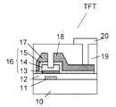
図2において、薄膜トランジスタTFTはいわゆるボトムゲート型と称される構成となっている。すなわち、ゲート電極11を被うゲート絶縁膜12上に多結晶半導体膜13、非晶質半導体膜14、高濃度不純物がドープされた非晶質半導体膜(高濃度ドープト非晶質半導体膜)15の順次積層体(半導体膜積層体16)が島状に形成されている。半導体膜積層体16の上面には、ドレイン電極17、ソース電極18が形成されている。この場合、ドレイン電極17とソース電極18の間の高濃度ドープト非晶質半導体層15はその下層の非晶質半導体膜14が露出する程度に除去され、オーミックコンタクト層として機能するようになっている。ドレイン電極17、ソース電極18は、それぞれ、島状に形成された半導体膜積層体16の側壁面に沿い該半導体膜積層体16の外周部にまで延在されて形成されている。 In FIG. 2, the thin film transistor TFT has a so-called bottom gate type. That is, a
なお、薄膜トランジスタTFTにおけるドレイン電極およびソース電極は、バイアスの印加状態によって入れ変わって動作するが、この明細書では、説明の便宜上、図中左側の電極をドレイン電極、図中右側の電極をソース電極と称する。また、ドレイン電極およびソース電極のうち一方の電極を第1電極、他方の電極を第2電極と称する場合がある。 Note that the drain electrode and the source electrode in the thin film transistor TFT operate in accordance with the bias application state. In this specification, for convenience of explanation, the left electrode in the figure is the drain electrode, and the right electrode in the figure is the source electrode. Called. In addition, one of the drain electrode and the source electrode may be referred to as a first electrode, and the other electrode may be referred to as a second electrode.
また、下記非特許文献1には、図3に示すような薄膜トランジスタTFTの構成が開示されている。図3は、図2に対応して描いた図となっている。図3において、図2の場合と比較して異なる構成は、高濃度ドープト非晶質半導体膜15は、非晶質半導体膜14の表面のみならず、島状に形成された半導体膜積層体(非晶質半導体膜14、多結晶半導体膜13)の側壁面に沿い該半導体膜積層体の外周部にまで延在されて形成されているとともに、ドレイン電極17、ソース電極18は、前記高濃度ドープト非晶質半導体膜15上に重畳されて形成されている。
図2に記載された薄膜トランジスタTFTは、チャネルが形成されるゲート絶縁膜12と半導体膜の界面において該半導体層が多結晶半導体層13で形成されている。このため、いわゆるS値および信頼性において良好で、非晶質半導体膜14からの水素供給によってリーク低減が図れるようになる。しかし、オフ状態において、ドレイン電極17とソース電極18との間に漏れ電流が発生することが指摘されている。半導体膜積層体16の側壁面から露出されている多結晶半導体膜13がドレイン電極17およびソース電極18に接触しているからだと考えられる。 In the thin film transistor TFT illustrated in FIG. 2, the semiconductor layer is formed of a
これに対して、図3に記載された薄膜トランジスタTFTは、ドレイン電極17およびソース電極18の多結晶半導体膜13との直接の接触はないことから、オフ状態における漏れ電流の発生を低減できるようになる。しかし、低いゲート電圧において電流にばらつきが生じることが指摘されるに至った。これは、オン状態における主たる電流経路は、高濃度ドープト非晶質半導体膜15→ノンドープ非晶質半導体膜14→多結晶半導体膜13→ノンドープ非晶質半導体膜14→高濃度ドープト非晶質半導体膜15となるが、高濃度ドープト非晶質半導体膜15→多結晶半導体膜13→高濃度ドープト非晶質半導体膜15という電流経路が、先の電流経路より低いゲート電圧で流れ始めてしまうことが原因となると考えられる。 In contrast, the thin film transistor TFT described in FIG. 3 has no direct contact between the
本発明の目的は、低リークで特性のばらつきの少ない薄膜トランジスタを備えた表示装置を提供することにある。 An object of the present invention is to provide a display device including a thin film transistor with low leakage and little variation in characteristics.
本発明の他の目的は、製造工数の低減が図れる表示装置の製造方法を提供することにある。 Another object of the present invention is to provide a method of manufacturing a display device that can reduce the number of manufacturing steps.
本発明の表示装置は、その薄膜トランジスタにおいて、ドレイン電極から延在される配線の直下およびソース電極から延在される配線の直下のそれぞれに半導体膜積層体が形成されるように構成することにより、前記半導体層膜積層体内の多結晶半導体層あるいは高濃度ドープト非晶質半導体膜がドレイン電極から延在される配線、およびソース電極から延在される配線と電気的に接続されることのないようにしたものである。 The display device of the present invention is configured such that in the thin film transistor, a semiconductor film stack is formed immediately below the wiring extending from the drain electrode and directly below the wiring extending from the source electrode, The polycrystalline semiconductor layer or the heavily doped amorphous semiconductor film in the semiconductor layer film stack is not electrically connected to the wiring extending from the drain electrode and the wiring extending from the source electrode. It is a thing.
本発明の構成は、たとえば、以下のようなものとすることができる。 The configuration of the present invention can be as follows, for example.
(1)本発明の表示装置は、表示部を備える基板に薄膜トランジスタが形成された表示装置であって、
前記薄膜トランジスタは、ゲート電極と、前記ゲート電極を被って形成されたゲート絶縁膜と、
前記ゲート絶縁膜の上面に前記ゲート電極を跨って形成された、少なくとも、多結晶半導体膜、非晶質半導体膜の順次積層体からなる半導体膜積層体と、
前記半導体膜積層体の上面に前記ゲート電極に重なる領域を間にして互いに対向して配置される第1電極と第2電極を備え、
前記第1電極から延在される配線の直下および前記第2電極から延在される配線の直下のそれぞれに前記半導体膜積層体が形成された構成からなることを特徴とする。(1) The display device of the present invention is a display device in which a thin film transistor is formed on a substrate including a display unit,
The thin film transistor includes a gate electrode, a gate insulating film formed over the gate electrode,
A semiconductor film stack formed of a sequential stack of at least a polycrystalline semiconductor film and an amorphous semiconductor film, which is formed across the gate electrode on the upper surface of the gate insulating film;
A first electrode and a second electrode disposed on the upper surface of the semiconductor film stack and facing each other with a region overlapping the gate electrode interposed therebetween;
The semiconductor film laminate is formed immediately below the wiring extending from the first electrode and directly below the wiring extending from the second electrode.
(2)本発明の表示装置は、(1)において、前記表示部は複数の画素の集合から構成され、前記薄膜トランジスタは前記各画素の領域に形成されていることを特徴とする。(2) The display device according to the present invention is characterized in that, in (1), the display section includes a set of a plurality of pixels, and the thin film transistor is formed in a region of each pixel.
(3)本発明の表示装置は、(1)において、前記表示部は複数の画素の集合から構成され、前記表示部に隣接して前記各画素を駆動させる駆動回路が形成され、前記薄膜トランジスタは前記駆動回路内に形成されていることを特徴とする。(3) In the display device of the present invention according to (1), the display unit is configured by a set of a plurality of pixels, and a driving circuit for driving the pixels is formed adjacent to the display unit. It is formed in the drive circuit.
(4)本発明の表示装置は、表示部を備える基板に薄膜トランジスタが形成された表示装置であって、
前記薄膜トランジスタは、ゲート電極と、前記ゲート電極を被って形成されたゲート絶縁膜と、
前記ゲート絶縁膜の上面に前記ゲート電極を跨って形成された、少なくとも、多結晶半導体膜、非晶質半導体膜、および高濃度ドープト非晶質半導体膜の順次積層体からなる半導体膜積層体と、
前記半導体膜積層体の上面に前記ゲート電極に重なる領域を間にして互いに対向して配置される第1電極と第2電極を備え、
前記第1電極と第2電極の間の前記高濃度ドープト非晶質半導体層はその下層の非晶質半導体膜が露出するまで除去され、
前記第1電極から延在される配線の直下および前記第2電極から延在される配線の直下のそれぞれに前記半導体膜積層体が形成された構成からなることを特徴とする。(4) The display device of the present invention is a display device in which a thin film transistor is formed on a substrate including a display unit,
The thin film transistor includes a gate electrode, a gate insulating film formed over the gate electrode,
A semiconductor film stack formed of a sequential stack of at least a polycrystalline semiconductor film, an amorphous semiconductor film, and a highly doped amorphous semiconductor film, formed over the gate electrode on the upper surface of the gate insulating film; ,
A first electrode and a second electrode disposed on the upper surface of the semiconductor film stack and facing each other with a region overlapping the gate electrode interposed therebetween;
The heavily doped amorphous semiconductor layer between the first electrode and the second electrode is removed until the underlying amorphous semiconductor film is exposed,
The semiconductor film laminate is formed immediately below the wiring extending from the first electrode and directly below the wiring extending from the second electrode.
(5)本発明の表示装置は、(4)において、前記表示部は複数の画素の集合から構成され、前記薄膜トランジスタは前記各画素の領域に形成されていることを特徴とする。(5) The display device of the present invention is characterized in that, in (4), the display section is composed of a set of a plurality of pixels, and the thin film transistor is formed in the area of each pixel.
(6)本発明の表示装置は、(4)において、前記表示部は複数の画素の集合から構成され、前記表示部に隣接して前記各画素を駆動させる駆動回路が形成され、前記薄膜トランジスタは前記駆動回路内に形成されていることを特徴とする。(6) In the display device according to the present invention, in (4), the display unit includes a set of a plurality of pixels, and a driving circuit that drives the pixels is formed adjacent to the display unit. It is formed in the drive circuit.
(7)本発明の表示装置の製造方法は、表示部を備える基板に薄膜トランジスタが形成された表示装置の製造方法であって、
前記薄膜トランジスタは、
少なくともゲート電極を被ってゲート絶縁膜を形成する行程と、
前記ゲート絶縁膜の上面に、少なくとも、多結晶半導体膜、非晶質半導体膜、高濃度ドープト非晶質半導体膜、金属膜を順次形成する行程と、
前記金属膜上に、前記薄膜トランジスタの形成しようとする第1電極と第2電極の間の領域において膜厚が小さく前記第1電極およびこの第1電極から延在される配線および前記第2電極およびこの第2電極から延在される配線の形成領域において膜厚の大きなフォトレジスト膜を形成する行程と、
前記フォトレジスト膜をマスクとし、前記高濃度ドープト非晶質半導体膜、前記非晶質半導体膜、前記多結晶半導体膜を順次エッチングする行程と、
前記フォトレジスト膜をアッシングにより前記薄膜トランジスタの形成しようとする第1電極と第2電極の間の領域において開口を形成する行程と、
前記開口が形成された前記フォトレジスト膜をマスクとして前記金属膜、前記高濃度ドープト非晶質半導体膜をその下層の非晶質半導体膜が露出する程度にエッチングする行程と、
を経て形成されることを特徴とする。(7) A manufacturing method of a display device of the present invention is a manufacturing method of a display device in which a thin film transistor is formed on a substrate including a display unit,
The thin film transistor
Forming a gate insulating film covering at least the gate electrode;
A step of sequentially forming at least a polycrystalline semiconductor film, an amorphous semiconductor film, a highly doped amorphous semiconductor film, and a metal film on the upper surface of the gate insulating film;
On the metal film, in the region between the first electrode and the second electrode where the thin film transistor is to be formed, the first electrode, the wiring extending from the first electrode, the second electrode, Forming a photoresist film having a large film thickness in a wiring formation region extending from the second electrode;
Using the photoresist film as a mask, a step of sequentially etching the highly doped amorphous semiconductor film, the amorphous semiconductor film, and the polycrystalline semiconductor film;
Forming an opening in a region between the first electrode and the second electrode where the thin film transistor is to be formed by ashing the photoresist film;
Etching the metal film and the heavily doped amorphous semiconductor film to the extent that the amorphous semiconductor film underneath is exposed using the photoresist film in which the opening is formed as a mask; and
It is formed through this process.
(8)本発明の表示装置の製造方法は、(7)において、膜厚が小さい領域と大きな領域をもつ前記フォトレジスト膜は、ハーフトーンマスクによる露光によって形成することを特徴とする。(8) The method for manufacturing a display device according to the present invention is characterized in that, in (7), the photoresist film having a small film thickness region and a large film region is formed by exposure with a halftone mask.
(9)本発明の表示装置の製造方法は、(7)において、膜厚が小さい領域と大きな領域をもつ前記フォトレジスト膜は、グレートーンマスクによる露光によって形成することを特徴とする。(9) The method for manufacturing a display device according to the present invention is characterized in that, in (7), the photoresist film having a small film thickness region and a large film region is formed by exposure with a gray-tone mask.
なお、上記した構成はあくまで一例であり、本発明は、技術思想を逸脱しない範囲内で適宜変更が可能である。また、上記した構成以外の本発明の構成の例は、本願明細書全体の記載または図面から明らかにされる。 The above-described configuration is merely an example, and the present invention can be modified as appropriate without departing from the technical idea. Further, examples of the configuration of the present invention other than the above-described configuration will be clarified from the entire description of the present specification or the drawings.
このように構成した表示装置によれば、低リークで特性のばらつきの少ない薄膜トランジスタを備えたものが得られる。 According to the display device configured as described above, a display device including a thin film transistor with low leakage and little variation in characteristics can be obtained.
また、このように構成した表示装置の製造方法によれば、製造工数の低減が図れる。 In addition, according to the display device manufacturing method configured as described above, the number of manufacturing steps can be reduced.
本発明のその他の効果については、明細書全体の記載から明らかにされる。 Other effects of the present invention will become apparent from the description of the entire specification.
本発明の実施例を図面を参照しながら説明する。なお、各図および各実施例において、同一または類似の構成要素には同じ符号を付し、説明を省略する。 Embodiments of the present invention will be described with reference to the drawings. In each drawing and each example, the same or similar components are denoted by the same reference numerals and description thereof is omitted.
〈実施例1〉
(表示装置の構成)
図6は、本発明の表示装置として有機EL表示装置を揚げ、その等価回路を示した図である。<Example 1>
(Configuration of display device)
FIG. 6 is a diagram showing an equivalent circuit of an organic EL display device as a display device of the present invention.
図6において、図中x方向に延在するゲート線103が図中y方向に並設されて形成されている。これらゲート線103は、その一端側においてゲートドライバ120に接続され、走査信号が順次供給されるようになっている。また、ゲート線103に近接されて図中x方向に延在する電力供給線104が図中y方向に並設されて形成されている。そして、図中y方向に延在するドレイン線102が図中x方向に並設されて形成されている。これらドレイン線102は、その一端側においてドレインドライバ121に接続され、映像信号が供給されるようになっている。また、ドレイン線102に近接されて図中y方向に延在するコモン線105が図中x方向に並設されて形成されている。 In FIG. 6,
図中点線枠で囲まれる領域を画素101の領域とし、表示領域はマトリックス状に配置される複数の画素101の集合体で構成されるようになっている。画素101の領域には、スイッチング素子110a、補助容量111、電流制御素子110b、有機EL素子112が形成されている。ゲート線103からの走査信号の供給によってスイッチング素子110aがオンし、補助容量111に電荷が蓄積され、その電荷が電流制御素子110bに流れる電流を制御する。そして、この電流は電力供給線104、有機EL素子112、電流制御素子110b、コモン線105を通して流れ、この電流の値に対応した輝度で有機EL素子112が発光するようになっている。 A region surrounded by a dotted frame in the figure is a region of the
なお、ゲートドライバ120、ドレインドライバ121は、画素101が形成される基板に形成されていても、あるいは外付けのLSIチップとして形成してもよい。 Note that the
図1(a)は、基板上に形成される前記画素101の構成を具体的に示した平面図である。図1(a)は、図中の画素電極20上に積層されて形成されるホール輸送層、発光層、電子輸送層、および陰極電極を省略して示しており、このため、図6に示す有機EL素子112、電力供給線104は描画されていないものとなっている。また、図1(b)は図1(a)のb−b線における断面図である。 FIG. 1A is a plan view specifically showing the configuration of the
図1(a)、(b)において、基板10の表面に、ゲート線103とこのゲート線に一体に形成されたゲート電極(スイッチング素子110aのゲート電極)、補助容量111の一方の電極111aとこの電極111aに一体に形成されたゲート電極(電流制御素子110bのゲート電極11)が金属膜によって形成されている。そして、これら金属膜を被ってゲート絶縁膜12が形成され、このゲート絶縁膜12の上面には、多結晶半導体膜13、ノンドープ非晶質半導体膜14、高濃度ドープト非晶質半導体膜15の順次積層体からなる半導体積層膜16が形成されている。 1A and 1B, on the surface of the
半導体積層膜16は、薄膜トランジスタからなるスイッチング素子110a、電流制御素子110bの形成領域だけでなく、これらスイッチング素子110a、電流制御素子110bのドレイン電極、ソース電極から延在される配線(ドレイン線102、コモン線105、補助容量の他方の電極111b等)の下層にも形成されている。半導体積層膜16は、後に示す製造方法の説明から明らかとなるように、該半導体積層膜16上のドレイン線102、コモン線105、補助容量の他方の電極111b等の形成の際に用いたフォトレジスト膜をマスクとしてエッチングすることにより形成されるからである。 The
これにより、図1(b)に示すように、ドレイン線102、コモン線105等の金属膜の下方には必ず半導体積層膜16が形成され、該半導体積層膜16は、多結晶半導体膜13、ノンドープ非晶質半導体膜14、および高濃度ドープト非晶質半導体膜15の順次積層体からなる。このため、金属膜と多結晶半導体膜13との電気的接触、あるいは高濃度ドープト非晶質半導体膜15と多結晶半導体膜13との電気的接触を回避して構成できる。したがって、たとえば、電流制御素子110bにおいて、漏れ電流を大幅に低減でき、低ゲート電圧における電流のばらつきを抑制できる構成とすることができる。このような構成は、スイッチング素子110aにおいても同様である。 As a result, as shown in FIG. 1B, the
なお、図1(b)に示すように、電流制御素子110bのドレイン電極17とソース電極18の間のチャネル領域において、高濃度ドープト非晶質半導体膜15が完全にエッチングされ、多結晶半導体膜13が若干の凹陥部を有する程度にエッチングされている。このエッチングにより、ドレイン電極17とソース電極18の電気的分離がなされている。 As shown in FIG. 1B, the heavily doped
基板10の表面には、スイッチング素子110a、電流制御素子110a等を被って、プラズマCVD法によって酸窒化シリコン膜からなる層間絶縁膜19が形成され、この層間絶縁膜19の上面にはたとえばITO(Indium Tin Oxide)からなる透明導電膜によって画素電極20が形成されている。この画素電極20は層間絶縁膜19に予め形成されたコンタクト孔CHを通して電流制御素子110bのドレイン電極18に接続されている。 An interlayer insulating
なお、層間絶縁膜19上には、画素電極20の形成と同時に形成される導電膜CNLが形成され、層間絶縁膜19に形成されたコンタクト孔を通して前記導電膜CNLに接続されるスイッチング素子110aのソース電極と、層間絶縁膜19、ゲート絶縁膜12に形成されたコンタクト孔CH1、CH2を通して前記導電膜CNLに接続される電流制御素子110bのゲート電極11が電気的に接続されるようになっている。 A conductive film CNL formed simultaneously with the formation of the
(表示装置の製造方法)
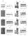
図4は、本発明の表示装置の製造方法の一実施例を示す行程図である。図4は、図1(a)の点線枠αの部分を示し、左側において平面図を、右側において断面図(前記平面図の一点鎖線における断面図)を示している。以下、行程順に説明をする。(Manufacturing method of display device)
FIG. 4 is a process chart showing an embodiment of a method for manufacturing a display device of the present invention. FIG. 4 shows a portion of the dotted line frame α in FIG. 1A, and shows a plan view on the left side and a cross-sectional view on the right side (a cross-sectional view along the dashed line in the plan view). Hereinafter, the description will be made in the order of the strokes.
行程1.(図4(a))
まず、ガラスからなる基板10を用意し、この基板10の表面にたとえばタングステン膜をスパッタ法によって形成し、周知のフォトリソグラフィ技術(1回目のフォト行程)による選択エッチング法によってゲート線103およびゲート電極11を形成する。さらに、基板10の表面にゲート線103等をも被って窒化シリコン膜および酸化シリコン膜の順次積層体からなるゲート絶縁膜12を形成する。前記窒化シリコン膜はアルカリイオンバリアとして機能し、酸化シリコン膜は後の行程で形成される半導体層との界面を良好な状態にできるようになっている。
First, a
行程2.(図4(b))
ゲート絶縁膜12の表面にたとえば多結晶シリコンからなる多結晶半導体膜13を形成する。多結晶半導体膜13は、たとえば、非晶質シリコン膜をプラズマCVD法で製膜したプリカーサー膜をアニール法により結晶化することにより得る。この場合、多結晶として粒径100nm以下のものを用いることによって特性ばらつきを少なくでき、いわゆるざらつきの少ない画像が得られるようになる。
A
行程3.(図4(c))
多結晶半導体膜13の形成に続き、プラズマCVD法を用いて、ノンドープ非晶質半導体膜14、高濃度ドープト非晶質半導体膜15を順次形成し、半導体積層膜16を形成する。さらに、スパッタ法を用いて、半導体積層膜16の上面にたとえばタングステンからなる金属膜MTを形成する。Step 3. (Fig. 4 (c))
Following the formation of the
行程4.(図4(d))
金属膜MTの上面にフォトレジストを塗布し前記金属膜MTを選択エッチングするためのマスクとなるフォトレジスト膜RSTを形成する(2回目のフォト行程)。この場合、いわゆるハーフトーンマスクあるいはグレートーンマスクを用いた露光によるフォトリソグラフィ技術によって、前記フォトレジスト膜RSTは、薄膜トランジスタのチャネル領域に相当する箇所において膜厚の小さな部分(左側の図面において斜線で示す)が形成されるようになっている。
A photoresist is applied on the upper surface of the metal film MT, and a photoresist film RST serving as a mask for selectively etching the metal film MT is formed (second photo process). In this case, the photoresist film RST is a portion having a small film thickness (indicated by hatching in the drawing on the left side) in a portion corresponding to the channel region of the thin film transistor by a photolithography technique by exposure using a so-called halftone mask or gray tone mask. ) Is formed.
行程5.(図4(e))
フォトレジスト膜RSTをマスクとし、該フォトレジスタ膜RSTから露出された金属膜MTをエッチングし、さらに、該金属膜MTのエッチングによって露出された半導体積層膜16を順次エッチングする。この段階では、薄膜トランジスタのドレイン電極およびソース電極はチャネル領域上にて互いに接続された状態となっている。Step 5. (Fig. 4 (e))
Using the photoresist film RST as a mask, the metal film MT exposed from the photoresist film RST is etched, and the semiconductor laminated
行程6.(図4(f))
フォトレジスト膜RSTにアッシングを施し、その厚さを均等に薄くすることによって、薄膜トランジスタのチャネル領域に相当する箇所に開口が形成され、前記金属膜の表面を露出させる。薄膜トランジスタのドレイン電極およびソース電極の形成領域に相当する箇所において前記フォトレジスト膜RSTは残存されたままとなる。Step 6. (Fig. 4 (f))
By ashing the photoresist film RST and uniformly reducing the thickness thereof, an opening is formed in a portion corresponding to the channel region of the thin film transistor, and the surface of the metal film is exposed. The photoresist film RST remains in a portion corresponding to the drain electrode and source electrode formation region of the thin film transistor.
アッシング後のフォトレジスト膜RSTをマスクとして、薄膜トランジスタのチャネル領域に相当する箇所の金属膜MT、高濃度ドープト非晶質半導体膜15を順次エッチングし、さらに、ノンドープ非晶質半導体膜14の表面において凹陥部が形成できる程度のエッチングを行う。このエッチングはいわゆるバックチャネルエッチングと称され、薄膜トランジスタのドレイン電極17とソース電極18との電気的な分離がなされるようになる。 Using the photoresist film RST after ashing as a mask, the metal film MT and the heavily doped
このような構成において、ドレイン電極17、ソース電極18等の金属膜MTの下方には必ず半導体積層膜16が形成され、該半導体積層膜16は、多結晶半導体膜13、ノンドープ非晶質半導体膜14、および高濃度ドープト非晶質半導体膜15の順次積層体からなっている。このため、金属膜MTと多結晶半導体膜13との電気的接触、あるいは高濃度ドープト非晶質半導体膜15と多結晶半導体膜13との電気的接触がなく構成できるので、漏れ電流を大幅に低減でき、低ゲート電圧における電流のばらつきを抑制することができる。 In such a configuration, the semiconductor laminated
行程7.(図4(g))
以上のように加工した基板10の表面に、前記金属膜等をも被って、たとえば、ラズマCVD法によって酸窒化シリコン膜からなる層間絶縁膜19を形成する。そして、フォトリソグラフ技術(3回目のフォト行程)を用いて層間絶縁膜19にコンタクト孔CHを形成する。Step 7. (Fig. 4 (g))
An interlayer insulating
行程8.(図4(h))
層間絶縁膜19の表面に前記コンタクト孔CHをも被ってたとえばITO(Indium Tin Oxide)からなる透明導電膜を形成する。そして、フォトリソグラフ技術(4回目のフォト行程)を用いて透明導電膜を選択エッチングすることにより画素電極20を形成する。この画素電極20は前記コンタクト孔CHを通じて薄膜トランジスタのソース電極18と電気的に接続されて形成される。Step 8. (Fig. 4 (h))
A transparent conductive film made of, for example, ITO (Indium Tin Oxide) is formed on the surface of the
このような製造方法は、上述したように4回のフォト行程で済み、製造工程の低減を図ることができるようになる。 Such a manufacturing method requires four photo strokes as described above, and can reduce the number of manufacturing steps.
その後は、図に示していないが、次に示す行程を経て完成する。すなわち、前記画素電極20の上面に、ホール輸送層、発光層、電子輸送層、および陰極電極を順次積層させて形成することによって、有機EL素子(図6にて符号112に示す)を構成する。 そして、基板の周囲に複数の有機EL素子が形成された表示領域を囲むようにしてシール材を配置し、封止基板あるいは封止缶を用いて封止する。この場合、封止基板あるいは封止缶を用いず、保護フィルムの貼付、あるいは蒸着による保護膜の直接形成を行うようにしてもよい。 Thereafter, although not shown in the figure, the process is completed through the following steps. That is, an organic EL element (indicated by
このように構成された基板には、外部信号源からの表示信号がプリント基板を介して供給され、該表示信号は前記基板上に形成された駆動回路を駆動させるようになっている。 A display signal from an external signal source is supplied to the substrate configured in this way via a printed circuit board, and the display signal drives a drive circuit formed on the substrate.
〈実施例2〉
図5は、本発明の表示装置の製造方法の実施例2を示す行程図で、図4と対応させて描いた図となっている。<Example 2>
FIG. 5 is a process diagram showing Example 2 of the method for manufacturing a display device of the present invention, and is a diagram drawn corresponding to FIG.
この実施例2による製造方法は、フォトリソグラフィ技術においていわゆるハーフトーンマスクあるいはグレートーンマスクを用いることなく行うものとなっている。以下、行程順に説明をする。 The manufacturing method according to the second embodiment is performed without using a so-called halftone mask or gray tone mask in the photolithography technique. Hereinafter, the description will be made in the order of the strokes.
行程1.(図5(a))
まず、ガラスからなる基板10を用意し、この基板10の表面にたとえばタングステン膜をスパッタ法によって形成し、周知のフォトリソグラフィ技術(1回目のフォト行程)による選択エッチング法によってゲート線103およびゲート電極11を形成する。さらに、基板10の表面にゲート線103等をも被って窒化シリコン膜および酸化シリコン膜の順次積層体からなるゲート絶縁膜12を形成する。前記窒化シリコン膜はアルカリイオンバリアとして機能し、酸化シリコン膜は後の行程で形成される半導体層との界面を良好な状態にできるようになっている。
First, a
行程2.(図5(b))
ゲート絶縁膜12の表面にたとえば多結晶シリコンからなる多結晶半導体膜13を形成する。多結晶半導体膜13は、たとえば、非晶質シリコン膜をプラズマCVD法で製膜したプリカーサー膜をアニール法により結晶化することにより得る。この場合、多結晶として粒径100nm以下のものを用いることによって特性ばらつきを少なくでき、いわゆるざらつきの少ない画像が得られるようになる。そして、多結晶半導体膜13の形成に続き、プラズマCVD法を用いて、ノンドープ非晶質半導体膜14、高濃度ドープト非晶質半導体膜15を順次形成し、半導体積層膜16を形成する。さらに、スパッタ法を用いて、半導体積層膜16の上面にたとえばタングステンからなる金属膜MTを形成する。
A
行程3.(図5(c))
金属膜MTの上面にフォトリソグラフィ技術によってパターン化されたフォトレジスト膜(図示せず)を形成し(2回目のフォト行程)、このフォトレジスト膜をマスクとして金属膜MTをエッチングし、薄膜トランジスタのドレイン電極17およびソース電極18を形成する。Step 3. (Fig. 5 (c))
A photoresist film (not shown) patterned by a photolithography technique is formed on the upper surface of the metal film MT (second photo process), and the metal film MT is etched using this photoresist film as a mask, so that the drain of the thin
行程4.(図5(d))
フォトリソグラフィ技術によって、ドレイン電極17およびソース電極18を被うようにしてパターン化されたフォトレジスト膜RSTを形成する(3回目のフォト行程)。ドレイン電極17から延在されて形成される配線、およびソース電極18から延在されて形成される配線は前記フォトレジスト膜RSTから露出されるようになっている。すなわち、このフォトレジスト膜RSTは、薄膜トランジスタの半導体層(半導体積層膜16)の形成領域に対応するパターンとなっている。
A photoresist film RST patterned so as to cover the
行程5.(図5(e))
フォトレジスト膜RST、およびフォトレジスト膜RSTから露出された金属膜MTをマスクとして、高濃度ドープト非晶質半導体膜15、ノンドープ非晶質半導体膜14、多結晶半導体膜13を順次エッチングし、薄膜トランジスタの半導体層(半導体膜積層体16)を残存させる。この場合、薄膜トランジスタの半導体膜積層体16以外にも、金属膜MTの直下において、高濃度ドープト非晶質半導体膜15、ノンドープ非晶質半導体膜14、多結晶半導体膜13が残存されるようになる。Step 5. (Fig. 5 (e))
Using the photoresist film RST and the metal film MT exposed from the photoresist film RST as a mask, the heavily doped
したがって、このように構成した場合、ドレイン電極17、ソース電極18等の金属膜MTの下方には必ず半導体膜積層体16が形成され、該半導体膜積層体16は、多結晶半導体膜13、ノンドープ非晶質半導体膜14、および高濃度ドープト非晶質半導体膜15の順次積層体からなっている。このため、金属膜MTと多結晶半導体膜13との電気的接触、あるいは高濃度ドープト非晶質半導体膜15と多結晶半導体膜13との電気的接触がなく構成できるので、漏れ電流を大幅に低減でき、低ゲート電圧における電流のばらつきを抑制することができる。 Therefore, in such a configuration, the
行程6.(図5(f))
フォトレジスト膜RSTを除去し、金属膜MTから露出している高濃度ドープト非晶質半導体膜15をエッチングし、さらに、ノンドープ非晶質半導体膜14の表面において凹陥部が形成できる程度のエッチングを行う。このエッチングはいわゆるバックチャネルエッチングと称され、薄膜トランジスタのドレイン電極17とソース電極18との電気的な分離がなされるようになる。Step 6. (Fig. 5 (f))
The photoresist film RST is removed, the heavily doped
行程7.(図5(g))
以上のように加工した基板10の表面に、前記金属膜MT等をも被って、たとえば、プラズマCVD法によって酸窒化シリコン膜からなる層間絶縁膜19を形成する。そして、フォトリソグラフ技術(4回目のフォト行程)を用いて層間絶縁膜19にコンタクト孔CHを形成する。Step 7. (Fig. 5 (g))
The surface of the
行程8.(図5(h))
層間絶縁膜19の表面に前記コンタクト孔CHをも被ってたとえばITO(Indium Tin Oxide)からなる透明導電膜を形成する。そして、フォトリソグラフ技術(5回目のフォト行程)を用いて透明導電膜を選択エッチングすることにより画素電極20を形成する。この画素電極20は前記コンタクト孔を通じて薄膜トランジスタのソース電極18と電気的に接続されて形成される。Step 8. (Fig. 5 (h))
A transparent conductive film made of, for example, ITO (Indium Tin Oxide) is formed on the surface of the
その後は、図に示していないが、実施例1に示したと同様の行程を経ることにより、有機EL表示装置が完成する。 Thereafter, although not shown in the drawing, the organic EL display device is completed through the same process as shown in the first embodiment.
〈実施例3〉
図7は、本発明の表示装置として液晶表示装置を揚げ、その等価回路を示した図である。<Example 3>
FIG. 7 is a diagram showing an equivalent circuit of a liquid crystal display device as a display device of the present invention.
図8において、図中x方向に延在するゲート線103が図中y方向に並設されて形成されている。これらゲート線103は、その一端側においてゲートドライバ120に接続され、走査信号が順次供給されるようになっている。また、隣接する各ゲート線103の間には該ゲート線103と平行にコモン線105が形成されている。そして、図中y方向に延在するドレイン線102が図中x方向に並設されて形成されている。これらドレイン線102は、その一端側においてドレインドライバ121に接続され、映像信号が供給されるようになっている。 In FIG. 8,
隣接する一対のゲート線103と隣接する一対のドレイン線102によって囲まれる領域を画素101の領域とし、表示領域はマトリックス状に配置される複数の画素101の集合体で構成されるようになっている。画素101の領域には、スイッチング素子110、補助容量111、一対の電極(画素電極、対向電極)が形成されている。ゲート線103からの走査信号の供給によってスイッチング素子110がオンし、ドレイン線102からの映像信号が画素電極に供給されるようになっている。画素電極と対向電極との間の電位差に応じた電界が液晶113に生じ、液晶113が駆動されるようになっている。補助容量111は、画素電極に供給された映像信号を比較的長く蓄積させるために設けられている。なお、ゲートドライバ120、ドレインドライバ121は、画素101が形成される基板に形成されていても、あるいは外付けのLSIチップとして形成してもよい。 The region surrounded by the pair of
図8(a)は、液晶を介して対向配置される各基板のうち一方の基板の該液晶側の面に形成される前記画素101の構成を具体的に示した平面図を示している。また、図8(b)は図8(a)のb−b線における断面図である。 FIG. 8A is a plan view specifically showing the configuration of the
図8(a)、(b)において、基板10の表面に、ゲート線103とこのゲート線103に一体に形成されたゲート電極11(スイッチング素子110のゲート電極)、補助容量111の一方の電極を構成するコモン線105が金属膜によって形成されている。そして、これら金属膜を被ってゲート絶縁膜12が形成され、このゲート絶縁膜12の上面には、多結晶半導体膜13、ノンドープ非晶質半導体膜14、高濃度ドープト非晶質半導体膜15の順次積層体からなる半導体膜積層体16が形成されている。 8A and 8B, on the surface of the
半導体膜積層体16は、スイッチング素子110の形成領域だけでなく、これらスイッチング素子110のドレイン電極17、ソース電極18に接続される配線(ドレイン線102、補助容量の他方の電極111等)の下層にも形成されている。半導体膜積層体16は、後に示す製造方法の説明から明らかとなるように、該半導膜体積層体16上のドレイン線102、補助容量の他方の電極111b等の形成の際に用いたフォトレジスト膜をマスクとしてエッチングすることにより形成されるからである。 The
これにより、図1(b)に示すように、ドレイン線102等の金属膜の下方には必ず半導体膜積層体16が形成され、該半導体膜積層体16は、多結晶半導体膜13、ノンドープ非晶質半導体膜14、および高濃度ドープト非晶質半導体膜15の順次積層体からなる。このため、金属膜と多結晶半導体膜13との電気的接触、あるいは高濃度ドープト非晶質半導体膜15と多結晶半導体膜13との電気的接触を回避して構成できる。したがって、電流制御素子110aにおいて、漏れ電流を大幅に低減でき、低ゲート電圧における電流のばらつきを抑制できる構成とすることができる。 As a result, as shown in FIG. 1B, a
なお、図8(b)に示すように、スイッチング素子110のドレイン電極17とソース電極18の間のチャネル領域において、高濃度ドープト非晶質半導体膜15が完全にエッチングされ、多結晶半導体膜13が若干の凹陥部を有する程度にエッチングされている。このエッチングにより、ドレイン電極とソース電極の電気的分離がなされている。 As shown in FIG. 8B, in the channel region between the
基板10の表面には、スイッチング素子110、補助容量等を被って層間絶縁膜19が形成され、この層間絶縁膜19の上面にはたとえばITO(Indium Tin Oxide)からなる透明導電膜によって画素電極20が形成されている。この画素電極20は層間絶縁膜19に予め形成されたコンタクト孔CHを通してスイッチング素子110のソース電極に接続されている。 An interlayer insulating
なお、この実施例の場合、前記画素電極20と対をなす電極(対向電極)は、液晶を介して配置される他方の基板の液晶側の面に形成されるようになっている(このような方式を縦電界方式と称する場合がある)。しかし、これに限らず、前記対向電極は基板10側に形成されていてもよい(このような方式を横電界方式と称する場合がある)。 In this embodiment, the electrode (counter electrode) paired with the
〈実施例4〉
上述した実施例では、基板としてたとえばガラス基板を示したものであるが、たとえば樹脂等からなるフレキシブルな基板であってもよい。有機EL表示装置で光を素子形成面に取り出す場合、いわゆるトップエミッション型の場合では、金属基板であってもよい。このようにした場合、耐衝撃性の優れた表示装置を得ることができる。<Example 4>
In the embodiment described above, for example, a glass substrate is shown as the substrate, but a flexible substrate made of resin or the like may be used. When light is extracted to the element formation surface in the organic EL display device, in the case of a so-called top emission type, a metal substrate may be used. In such a case, a display device having excellent impact resistance can be obtained.
〈実施例5〉
上述した実施例では、画素内に形成する薄膜トランジスタは、その機能に基づき1個形成したものである。しかし、複数の薄膜トランジスタをたとえば直列接続させて構成するようにしてもよい。このようにした場合、点在して偶発的に発生する漏れ電流の大きい薄膜トランジスタによる表示欠陥を低減することができる。<Example 5>
In the embodiment described above, one thin film transistor formed in a pixel is formed based on its function. However, a plurality of thin film transistors may be connected in series, for example. In this case, it is possible to reduce display defects due to thin film transistors having a large leakage current that are scattered and accidentally generated.
〈実施例6〉
上述した実施例では、半導体の材料としてシリコンを用いたものであるが、これに限定されることなく、たとえば、SiGe等からなる他の半導体材料であってもよい。<Example 6>
In the above-described embodiments, silicon is used as a semiconductor material, but the present invention is not limited to this. For example, other semiconductor materials made of SiGe or the like may be used.
〈実施例7〉
上述した実施例では、薄膜トランジスタのゲート絶縁膜を窒化膜と酸化膜の積層構造としたものである。しかし、酸窒化シリコン膜であってもよい。アルカリイオンバリア性能と信頼性を両立させることができる。また、窒化膜、あるいは酸化膜のいずれか一方のみで形成するようにしてもよい。<Example 7>
In the embodiment described above, the gate insulating film of the thin film transistor has a laminated structure of a nitride film and an oxide film. However, it may be a silicon oxynitride film. Alkali ion barrier performance and reliability can both be achieved. Further, it may be formed of only one of a nitride film and an oxide film.
〈実施例8〉
上述した実施例では、薄膜トランジスタの半導体層として用いられる多結晶シリコン膜は、ランプアニール法を用いて形成したが、これに限らず、レーザーアニール法、熱CVD法、プラズマCVD法、あるいはCatCVD法を用いて形成するようにしてもよい。<Example 8>
In the above-described embodiments, the polycrystalline silicon film used as the semiconductor layer of the thin film transistor is formed by using the lamp annealing method. However, the present invention is not limited to this, and laser annealing, thermal CVD, plasma CVD, or CatCVD is used. You may make it form using.
〈実施例9〉
上述した実施例では、薄膜トランジスタの半導体層として用いられる多結晶シリコン膜は、不純物をドーピングしないものを用いたものである。しかし、これに限らず、たとえば、オフ状態で導通しない程度に低濃度の不純物をドーピングするようにしてもよい。ドーピングは、プリカーサー膜の製膜時におけるin-situドーピング、あるいはイオン注入法を用いて行うことができる。このようにした場合、薄膜トランジスタの閾値の制御ができるようになる。<Example 9>
In the above-described embodiment, the polycrystalline silicon film used as the semiconductor layer of the thin film transistor is a film not doped with impurities. However, the present invention is not limited to this. For example, a low-concentration impurity may be doped so as not to conduct in the off state. Doping can be performed using in-situ doping during the formation of the precursor film or ion implantation. In this case, the threshold value of the thin film transistor can be controlled.
〈実施例10〉
上述した実施例では、薄膜トランジスタの半導体層として用いられる高濃度ドープト非晶質半導体膜は、n型、p型の種類を示すことなく説明したが、それらのいずれであってもよい。<Example 10>
In the above-described embodiments, the heavily doped amorphous semiconductor film used as the semiconductor layer of the thin film transistor has been described without showing n-type and p-type types, but any of them may be used.
〈実施例11〉
上述した実施例では、半導体膜積層体は、オーミックコンタクト層として機能する高濃度ドープト非晶質半導体膜を備えた構成として説明したが、該高濃度ドープト非晶質半導体膜を備えていない構成としてもよい。この場合であっても、多結晶半導体膜とドレイン電極およびソース電極等の金属膜と多結晶半導体膜の直接の接触を回避できることから本発明の効果を奏することができる。<Example 11>
In the above-described embodiments, the semiconductor film stack has been described as a configuration including a highly doped amorphous semiconductor film that functions as an ohmic contact layer. However, as a configuration not including the highly doped amorphous semiconductor film, Also good. Even in this case, the direct contact between the polycrystalline semiconductor film, the metal film such as the drain electrode and the source electrode, and the polycrystalline semiconductor film can be avoided, so that the effect of the present invention can be achieved.
〈実施例12〉
上述した実施例では、薄膜トランジスタの半導体層として用いられるノンドープ非晶質半導体膜と高濃度ドープト非晶質半導体膜は直接に当接した配置となっているように示した。しかし、これらの間に低濃度電界緩和層を介在させるように構成してもよい。リーク電流の発生をさらに低減できるからである。<Example 12>
In the above-described embodiments, the non-doped amorphous semiconductor film and the heavily doped amorphous semiconductor film used as the semiconductor layer of the thin film transistor are shown to be in direct contact with each other. However, a low concentration electric field relaxation layer may be interposed between them. This is because the generation of leakage current can be further reduced.
〈実施例13〉
上述した実施例では、薄膜トランジスタを被って形成される層間絶縁膜は、酸窒化シリコン膜として形成した。しかし、これに限らず、有機材料膜、あるいは無機材料膜と有機材料膜との積層体を前記層間絶縁膜として構成してもよい。このようにした場合、表面が平坦な状態で形成できる効果を奏する。<Example 13>
In the above-described embodiment, the interlayer insulating film formed over the thin film transistor is formed as a silicon oxynitride film. However, the present invention is not limited to this, and an organic material film or a laminate of an inorganic material film and an organic material film may be configured as the interlayer insulating film. When it does in this way, there exists an effect which can be formed in the state where the surface is flat.
〈実施例14〉
上述した実施例では、たとえば薄膜トランジスタのドレイン電極、ソース電極をタングステンからなる金属膜で構成したものである。しかし、これに限らず、クロム、モリブデン、アルミ、銅、あるいはこれらの合金であってもよい。このうち、アルミ、銅、あるいはこれらの合金は配線抵抗を低減させることができる。また、タングステン、クロム、モリブデン、あるいはこれらの合金は耐熱性が高く、プロセスの裕度を向上させることができる。<Example 14>
In the above-described embodiment, for example, the drain electrode and the source electrode of the thin film transistor are made of a metal film made of tungsten. However, it is not limited to this, and may be chromium, molybdenum, aluminum, copper, or an alloy thereof. Of these, aluminum, copper, or alloys thereof can reduce wiring resistance. In addition, tungsten, chromium, molybdenum, or an alloy thereof has high heat resistance and can improve the process tolerance.
〈実施例15〉
上述した実施例では、薄膜トランジスタTFTは各画素内に形成されたものを示したものである。しかし、同一の基板上において、各画素の集合からなる表示部の周辺に各画素を駆動させる駆動回路(ゲートドライバ120、ドレインドライバ121)を設け、この駆動回路を薄膜トランジスタで構成したものがある。この場合において、該駆動回路の薄膜トランジスタに本発明を適用することができる。<Example 15>
In the above-described embodiments, the thin film transistor TFT is formed in each pixel. However, a driver circuit (
以上、本発明を実施例を用いて説明してきたが、これまでの各実施例で説明した構成はあくまで一例であり、本発明は、技術思想を逸脱しない範囲内で適宜変更が可能である。また、それぞれの実施例で説明した構成は、互いに矛盾しない限り、組み合わせて用いてもよい。 The present invention has been described using the embodiments. However, the configurations described in the embodiments so far are only examples, and the present invention can be appropriately changed without departing from the technical idea. Further, the configurations described in the respective embodiments may be used in combination as long as they do not contradict each other.
10……基板、11……ゲート電極、12……ゲート絶縁膜、13……多結晶半導体膜、14……ノンドープ非晶質半導体膜、15……高濃度ドープト非晶質半導体膜、16……半導体膜積層体、17……ドレイン電極、18……ソース電極、19……層間絶縁膜、20……画素電極、101……画素、102……ドレイン線、103……ゲート線、104……電力供給線、105……コモン線、111……補助容量、112……有機EL素子、120……ゲートドライバ、121……ドレインドライバ、TFT……薄膜トランジスタ、MT……金属膜、RST……フォトレジスト膜。DESCRIPTION OF
Claims (9)
Translated fromJapanese前記薄膜トランジスタは、ゲート電極と、前記ゲート電極を被って形成されたゲート絶縁膜と、
前記ゲート絶縁膜の上面に前記ゲート電極を跨って形成された、少なくとも、多結晶半導体膜、非晶質半導体膜の順次積層体からなる半導体膜積層体と、
前記半導体膜積層体の上面に前記ゲート電極に重なる領域を間にして互いに対向して配置される第1電極と第2電極を備え、
前記第1電極から延在される配線の直下および前記第2電極から延在される配線の直下のそれぞれに前記半導体膜積層体が形成された構成からなることを特徴とする表示装置。A display device in which a thin film transistor is formed on a substrate including a display unit,
The thin film transistor includes a gate electrode, a gate insulating film formed over the gate electrode,
A semiconductor film stack formed of a sequential stack of at least a polycrystalline semiconductor film and an amorphous semiconductor film, which is formed across the gate electrode on the upper surface of the gate insulating film;
A first electrode and a second electrode disposed on the upper surface of the semiconductor film stack and facing each other with a region overlapping the gate electrode interposed therebetween;
A display device, comprising: a structure in which the semiconductor film stack is formed immediately below a wiring extending from the first electrode and immediately below a wiring extending from the second electrode.
前記薄膜トランジスタは、ゲート電極と、前記ゲート電極を被って形成されたゲート絶縁膜と、
前記ゲート絶縁膜の上面に前記ゲート電極を跨って形成された、少なくとも、多結晶半導体膜、非晶質半導体膜、および高濃度ドープト非晶質半導体膜の順次積層体からなる半導体膜積層体と、
前記半導体膜積層体の上面に前記ゲート電極に重なる領域を間にして互いに対向して配置される第1電極と第2電極を備え、
前記第1電極と第2電極の間の前記高濃度ドープト非晶質半導体層はその下層の非晶質半導体膜が露出するまで除去され、
前記第1電極から延在される配線の直下および前記第2電極から延在される配線の直下のそれぞれに前記半導体膜積層体が形成された構成からなることを特徴とする表示装置。A display device in which a thin film transistor is formed on a substrate including a display unit,
The thin film transistor includes a gate electrode, a gate insulating film formed over the gate electrode,
A semiconductor film stack formed of a sequential stack of at least a polycrystalline semiconductor film, an amorphous semiconductor film, and a highly doped amorphous semiconductor film, formed over the gate electrode on the upper surface of the gate insulating film; ,
A first electrode and a second electrode disposed on the upper surface of the semiconductor film stack and facing each other with a region overlapping the gate electrode interposed therebetween;
The heavily doped amorphous semiconductor layer between the first electrode and the second electrode is removed until the underlying amorphous semiconductor film is exposed,
A display device, comprising: a structure in which the semiconductor film stack is formed immediately below a wiring extending from the first electrode and immediately below a wiring extending from the second electrode.
前記薄膜トランジスタは、
少なくともゲート電極を被ってゲート絶縁膜を形成する行程と、
前記ゲート絶縁膜の上面に、少なくとも、多結晶半導体膜、非晶質半導体膜、高濃度ドープト非晶質半導体膜、金属膜を順次形成する行程と、
前記金属膜上に、前記薄膜トランジスタの形成しようとする第1電極と第2電極の間の領域において膜厚が小さく前記第1電極およびこの第1電極から延在される配線および前記第2電極およびこの第2電極から延在される配線の形成領域において膜厚の大きなフォトレジスト膜を形成する行程と、
前記フォトレジスト膜をマスクとし、前記金属膜、前記高濃度ドープト非晶質半導体膜、前記非晶質半導体膜、前記多結晶半導体膜を順次エッチングする行程と、
前記フォトレジスト膜をアッシングにより前記薄膜トランジスタの形成しようとする第1電極と第2電極の間の領域において開口を形成する行程と、
前記開口が形成された前記フォトレジスト膜をマスクとして前記金属膜、前記高濃度ドープト非晶質半導体膜をその下層の非晶質半導体膜が露出する程度にエッチングする行程と、
を経て形成されることを特徴とする表示装置の製造方法。A method of manufacturing a display device in which a thin film transistor is formed on a substrate including a display unit,
The thin film transistor
Forming a gate insulating film covering at least the gate electrode;
A step of sequentially forming at least a polycrystalline semiconductor film, an amorphous semiconductor film, a highly doped amorphous semiconductor film, and a metal film on the upper surface of the gate insulating film;
On the metal film, in the region between the first electrode and the second electrode where the thin film transistor is to be formed, the first electrode, the wiring extending from the first electrode, the second electrode, Forming a photoresist film having a large film thickness in a wiring formation region extending from the second electrode;
Etching the metal film, the heavily doped amorphous semiconductor film, the amorphous semiconductor film, and the polycrystalline semiconductor film in sequence using the photoresist film as a mask;
Forming an opening in a region between the first electrode and the second electrode where the thin film transistor is to be formed by ashing the photoresist film;
Etching the metal film and the heavily doped amorphous semiconductor film to the extent that the amorphous semiconductor film underneath is exposed using the photoresist film in which the opening is formed as a mask; and
A manufacturing method of a display device, wherein
Priority Applications (2)
| Application Number | Priority Date | Filing Date | Title |
|---|---|---|---|
| JP2008276287AJP2010108957A (en) | 2008-10-28 | 2008-10-28 | Display device and method of manufacturing the same |
| US12/606,284US8258024B2 (en) | 2008-10-28 | 2009-10-27 | Display device and method of manufacturing the same |
Applications Claiming Priority (1)
| Application Number | Priority Date | Filing Date | Title |
|---|---|---|---|
| JP2008276287AJP2010108957A (en) | 2008-10-28 | 2008-10-28 | Display device and method of manufacturing the same |
Publications (1)
| Publication Number | Publication Date |
|---|---|
| JP2010108957Atrue JP2010108957A (en) | 2010-05-13 |
Family
ID=42116618
Family Applications (1)
| Application Number | Title | Priority Date | Filing Date |
|---|---|---|---|
| JP2008276287APendingJP2010108957A (en) | 2008-10-28 | 2008-10-28 | Display device and method of manufacturing the same |
Country Status (2)
| Country | Link |
|---|---|
| US (1) | US8258024B2 (en) |
| JP (1) | JP2010108957A (en) |
Cited By (1)
| Publication number | Priority date | Publication date | Assignee | Title |
|---|---|---|---|---|
| JP2012014099A (en)* | 2010-07-05 | 2012-01-19 | Mitsubishi Electric Corp | Active matrix substrate and liquid crystal device |
Families Citing this family (6)
| Publication number | Priority date | Publication date | Assignee | Title |
|---|---|---|---|---|
| US8148733B2 (en)* | 2007-06-12 | 2012-04-03 | SemiLEDs Optoelectronics Co., Ltd. | Vertical LED with current guiding structure |
| US8546818B2 (en) | 2007-06-12 | 2013-10-01 | SemiLEDs Optoelectronics Co., Ltd. | Vertical LED with current-guiding structure |
| JP5111167B2 (en)* | 2008-03-06 | 2012-12-26 | 株式会社ジャパンディスプレイイースト | Liquid crystal display |
| KR101802406B1 (en)* | 2009-11-27 | 2017-11-28 | 가부시키가이샤 한도오따이 에네루기 켄큐쇼 | Semiconductor device and method for manufacturing the same |
| US20130069066A1 (en)* | 2011-09-21 | 2013-03-21 | Shenzhen China Star Optoelectronics Technology Co.,Ltd. | Thin film transistor and manufacture method thereof |
| JP2015090434A (en)* | 2013-11-06 | 2015-05-11 | 株式会社ジャパンディスプレイ | Liquid crystal display device and manufacturing method of the same |
Citations (5)
| Publication number | Priority date | Publication date | Assignee | Title |
|---|---|---|---|---|
| JP2002151522A (en)* | 2000-08-28 | 2002-05-24 | Sharp Corp | Active matrix substrate, method of manufacturing the same, and display device |
| JP2003057673A (en)* | 2001-08-13 | 2003-02-26 | Obayashi Seiko Kk | Active matrix display and manufacturing method thereof |
| JP2008053394A (en)* | 2006-08-24 | 2008-03-06 | Hitachi Displays Ltd | Manufacturing method of display device |
| JP2008109102A (en)* | 2006-10-23 | 2008-05-08 | Samsung Electronics Co Ltd | Method for manufacturing thin film transistor substrate |
| JP2008175842A (en)* | 2007-01-16 | 2008-07-31 | Hitachi Displays Ltd | Display device |
Family Cites Families (9)
| Publication number | Priority date | Publication date | Assignee | Title |
|---|---|---|---|---|
| JP3564417B2 (en)* | 2000-05-31 | 2004-09-08 | Nec液晶テクノロジー株式会社 | Color liquid crystal display device and method of manufacturing the same |
| KR100585873B1 (en)* | 2003-11-03 | 2006-06-07 | 엘지.필립스 엘시디 주식회사 | Polysilicon Liquid Crystal Display Device and Manufacturing Method Thereof |
| JP2005167051A (en) | 2003-12-04 | 2005-06-23 | Sony Corp | THIN FILM TRANSISTOR AND METHOD FOR PRODUCING THIN FILM TRANSISTOR |
| TWI292625B (en)* | 2006-01-02 | 2008-01-11 | Au Optronics Corp | Fabricating method for pixel structure |
| TWI275184B (en)* | 2006-05-18 | 2007-03-01 | Au Optronics Corp | Thin film transistor and fabrication method thereof |
| KR101261609B1 (en)* | 2006-07-06 | 2013-05-06 | 삼성디스플레이 주식회사 | Thin film transistor, thin film transistor array panel and method for manufacturing the same |
| KR101399608B1 (en)* | 2007-07-27 | 2014-05-26 | 가부시키가이샤 한도오따이 에네루기 켄큐쇼 | Method for manufacturing semiconductor device |
| JP5380037B2 (en)* | 2007-10-23 | 2014-01-08 | 株式会社半導体エネルギー研究所 | Method for manufacturing semiconductor device |
| TWI328788B (en)* | 2008-03-11 | 2010-08-11 | Au Optronics Corp | Gate driver-on-array and method of making the same |
- 2008
- 2008-10-28JPJP2008276287Apatent/JP2010108957A/enactivePending
- 2009
- 2009-10-27USUS12/606,284patent/US8258024B2/enactiveActive
Patent Citations (5)
| Publication number | Priority date | Publication date | Assignee | Title |
|---|---|---|---|---|
| JP2002151522A (en)* | 2000-08-28 | 2002-05-24 | Sharp Corp | Active matrix substrate, method of manufacturing the same, and display device |
| JP2003057673A (en)* | 2001-08-13 | 2003-02-26 | Obayashi Seiko Kk | Active matrix display and manufacturing method thereof |
| JP2008053394A (en)* | 2006-08-24 | 2008-03-06 | Hitachi Displays Ltd | Manufacturing method of display device |
| JP2008109102A (en)* | 2006-10-23 | 2008-05-08 | Samsung Electronics Co Ltd | Method for manufacturing thin film transistor substrate |
| JP2008175842A (en)* | 2007-01-16 | 2008-07-31 | Hitachi Displays Ltd | Display device |
Cited By (1)
| Publication number | Priority date | Publication date | Assignee | Title |
|---|---|---|---|---|
| JP2012014099A (en)* | 2010-07-05 | 2012-01-19 | Mitsubishi Electric Corp | Active matrix substrate and liquid crystal device |
Also Published As
| Publication number | Publication date |
|---|---|
| US20100102322A1 (en) | 2010-04-29 |
| US8258024B2 (en) | 2012-09-04 |
Similar Documents
| Publication | Publication Date | Title |
|---|---|---|
| TWI580021B (en) | Organic light emitting diode display and method of manufacturing same | |
| CN101523610B (en) | Thin film transistor, method for manufacturing the same, and display | |
| USRE48032E1 (en) | Thin-film semiconductor substrate, light-emitting panel, and method of manufacturing the thin-film semiconductor substrate | |
| JP5096437B2 (en) | Organic EL display device | |
| CN115810634A (en) | Display device | |
| JP7152448B2 (en) | display device | |
| KR100696479B1 (en) | Flat panel display and manufacturing method | |
| JP2001109404A (en) | EL display device | |
| CN102576711B (en) | The manufacture method of thin film transistor (TFT) array device, thin film transistor (TFT) array device | |
| JP2008258345A (en) | THIN FILM TRANSISTOR, MANUFACTURING METHOD THEREOF, AND DISPLAY DEVICE | |
| US20230061983A1 (en) | Display apparatus having an oxide semiconductor | |
| WO2012039000A1 (en) | Thin film transistor array device and method for manufacturing thin film transistor array device | |
| JP2010108957A (en) | Display device and method of manufacturing the same | |
| KR20210086247A (en) | Display apparatus | |
| US20060169984A1 (en) | Thin film transistor array panel | |
| JP2001100655A (en) | El display device | |
| JP4633434B2 (en) | Semiconductor device and manufacturing method thereof | |
| TW525403B (en) | Electroluminescence display device | |
| US8426863B2 (en) | Thin film transistor; method of manufacturing same; and organic light emitting device including the thin film transistor | |
| JP2022077412A (en) | Thin film transistor circuit | |
| KR100611158B1 (en) | Organic light emitting display | |
| TWI459566B (en) | Thin film transistor, display device therewith and method of manufacturing thin film transistor and display device | |
| JP5337414B2 (en) | Display device and manufacturing method thereof | |
| JP5687448B2 (en) | THIN FILM TRANSISTOR, DISPLAY DEVICE USING THE SAME, AND METHOD FOR PRODUCING THIN FILM TRANSISTOR | |
| KR101750562B1 (en) | Organic Light Emitting Display Device and Method for fabricating the same |
Legal Events
| Date | Code | Title | Description |
|---|---|---|---|
| A711 | Notification of change in applicant | Free format text:JAPANESE INTERMEDIATE CODE: A712 Effective date:20110218 | |
| RD03 | Notification of appointment of power of attorney | Free format text:JAPANESE INTERMEDIATE CODE: A7423 Effective date:20110218 | |
| A621 | Written request for application examination | Free format text:JAPANESE INTERMEDIATE CODE: A621 Effective date:20110613 | |
| A977 | Report on retrieval | Free format text:JAPANESE INTERMEDIATE CODE: A971007 Effective date:20130508 | |
| A131 | Notification of reasons for refusal | Free format text:JAPANESE INTERMEDIATE CODE: A131 Effective date:20130514 | |
| A521 | Request for written amendment filed | Free format text:JAPANESE INTERMEDIATE CODE: A523 Effective date:20130708 | |
| A131 | Notification of reasons for refusal | Free format text:JAPANESE INTERMEDIATE CODE: A131 Effective date:20140212 | |
| A02 | Decision of refusal | Free format text:JAPANESE INTERMEDIATE CODE: A02 Effective date:20140701 |