JP2010103329A - Method of manufacturing semiconductor device, and semiconductor device - Google Patents
Method of manufacturing semiconductor device, and semiconductor deviceDownload PDFInfo
- Publication number
- JP2010103329A JP2010103329AJP2008273818AJP2008273818AJP2010103329AJP 2010103329 AJP2010103329 AJP 2010103329AJP 2008273818 AJP2008273818 AJP 2008273818AJP 2008273818 AJP2008273818 AJP 2008273818AJP 2010103329 AJP2010103329 AJP 2010103329A
- Authority
- JP
- Japan
- Prior art keywords
- film
- cap
- dielectric constant
- cap film
- low
- Prior art date
- Legal status (The legal status is an assumption and is not a legal conclusion. Google has not performed a legal analysis and makes no representation as to the accuracy of the status listed.)
- Pending
Links
Images


Classifications
- H—ELECTRICITY
- H01—ELECTRIC ELEMENTS
- H01L—SEMICONDUCTOR DEVICES NOT COVERED BY CLASS H10
- H01L21/00—Processes or apparatus adapted for the manufacture or treatment of semiconductor or solid state devices or of parts thereof
- H01L21/70—Manufacture or treatment of devices consisting of a plurality of solid state components formed in or on a common substrate or of parts thereof; Manufacture of integrated circuit devices or of parts thereof
- H01L21/71—Manufacture of specific parts of devices defined in group H01L21/70
- H01L21/768—Applying interconnections to be used for carrying current between separate components within a device comprising conductors and dielectrics
- H01L21/76801—Applying interconnections to be used for carrying current between separate components within a device comprising conductors and dielectrics characterised by the formation and the after-treatment of the dielectrics, e.g. smoothing
- H01L21/7682—Applying interconnections to be used for carrying current between separate components within a device comprising conductors and dielectrics characterised by the formation and the after-treatment of the dielectrics, e.g. smoothing the dielectric comprising air gaps
- H—ELECTRICITY
- H01—ELECTRIC ELEMENTS
- H01L—SEMICONDUCTOR DEVICES NOT COVERED BY CLASS H10
- H01L21/00—Processes or apparatus adapted for the manufacture or treatment of semiconductor or solid state devices or of parts thereof
- H01L21/02—Manufacture or treatment of semiconductor devices or of parts thereof
- H01L21/02104—Forming layers
- H01L21/02107—Forming insulating materials on a substrate
- H01L21/02109—Forming insulating materials on a substrate characterised by the type of layer, e.g. type of material, porous/non-porous, pre-cursors, mixtures or laminates
- H01L21/02112—Forming insulating materials on a substrate characterised by the type of layer, e.g. type of material, porous/non-porous, pre-cursors, mixtures or laminates characterised by the material of the layer
- H01L21/02123—Forming insulating materials on a substrate characterised by the type of layer, e.g. type of material, porous/non-porous, pre-cursors, mixtures or laminates characterised by the material of the layer the material containing silicon
- H01L21/02126—Forming insulating materials on a substrate characterised by the type of layer, e.g. type of material, porous/non-porous, pre-cursors, mixtures or laminates characterised by the material of the layer the material containing silicon the material containing Si, O, and at least one of H, N, C, F, or other non-metal elements, e.g. SiOC, SiOC:H or SiONC
- H—ELECTRICITY
- H01—ELECTRIC ELEMENTS
- H01L—SEMICONDUCTOR DEVICES NOT COVERED BY CLASS H10
- H01L21/00—Processes or apparatus adapted for the manufacture or treatment of semiconductor or solid state devices or of parts thereof
- H01L21/02—Manufacture or treatment of semiconductor devices or of parts thereof
- H01L21/02104—Forming layers
- H01L21/02107—Forming insulating materials on a substrate
- H01L21/02109—Forming insulating materials on a substrate characterised by the type of layer, e.g. type of material, porous/non-porous, pre-cursors, mixtures or laminates
- H01L21/022—Forming insulating materials on a substrate characterised by the type of layer, e.g. type of material, porous/non-porous, pre-cursors, mixtures or laminates the layer being a laminate, i.e. composed of sublayers, e.g. stacks of alternating high-k metal oxides
- H—ELECTRICITY
- H01—ELECTRIC ELEMENTS
- H01L—SEMICONDUCTOR DEVICES NOT COVERED BY CLASS H10
- H01L21/00—Processes or apparatus adapted for the manufacture or treatment of semiconductor or solid state devices or of parts thereof
- H01L21/02—Manufacture or treatment of semiconductor devices or of parts thereof
- H01L21/02104—Forming layers
- H01L21/02107—Forming insulating materials on a substrate
- H01L21/02225—Forming insulating materials on a substrate characterised by the process for the formation of the insulating layer
- H01L21/0226—Forming insulating materials on a substrate characterised by the process for the formation of the insulating layer formation by a deposition process
- H01L21/02263—Forming insulating materials on a substrate characterised by the process for the formation of the insulating layer formation by a deposition process deposition from the gas or vapour phase
- H01L21/02271—Forming insulating materials on a substrate characterised by the process for the formation of the insulating layer formation by a deposition process deposition from the gas or vapour phase deposition by decomposition or reaction of gaseous or vapour phase compounds, i.e. chemical vapour deposition
- H—ELECTRICITY
- H01—ELECTRIC ELEMENTS
- H01L—SEMICONDUCTOR DEVICES NOT COVERED BY CLASS H10
- H01L21/00—Processes or apparatus adapted for the manufacture or treatment of semiconductor or solid state devices or of parts thereof
- H01L21/02—Manufacture or treatment of semiconductor devices or of parts thereof
- H01L21/02104—Forming layers
- H01L21/02107—Forming insulating materials on a substrate
- H01L21/02296—Forming insulating materials on a substrate characterised by the treatment performed before or after the formation of the layer
- H01L21/02318—Forming insulating materials on a substrate characterised by the treatment performed before or after the formation of the layer post-treatment
- H01L21/02345—Forming insulating materials on a substrate characterised by the treatment performed before or after the formation of the layer post-treatment treatment by exposure to radiation, e.g. visible light
- H01L21/02351—Forming insulating materials on a substrate characterised by the treatment performed before or after the formation of the layer post-treatment treatment by exposure to radiation, e.g. visible light treatment by exposure to corpuscular radiation, e.g. exposure to electrons, alpha-particles, protons or ions
- H—ELECTRICITY
- H01—ELECTRIC ELEMENTS
- H01L—SEMICONDUCTOR DEVICES NOT COVERED BY CLASS H10
- H01L21/00—Processes or apparatus adapted for the manufacture or treatment of semiconductor or solid state devices or of parts thereof
- H01L21/02—Manufacture or treatment of semiconductor devices or of parts thereof
- H01L21/04—Manufacture or treatment of semiconductor devices or of parts thereof the devices having potential barriers, e.g. a PN junction, depletion layer or carrier concentration layer
- H01L21/18—Manufacture or treatment of semiconductor devices or of parts thereof the devices having potential barriers, e.g. a PN junction, depletion layer or carrier concentration layer the devices having semiconductor bodies comprising elements of Group IV of the Periodic Table or AIIIBV compounds with or without impurities, e.g. doping materials
- H01L21/30—Treatment of semiconductor bodies using processes or apparatus not provided for in groups H01L21/20 - H01L21/26
- H01L21/31—Treatment of semiconductor bodies using processes or apparatus not provided for in groups H01L21/20 - H01L21/26 to form insulating layers thereon, e.g. for masking or by using photolithographic techniques; After treatment of these layers; Selection of materials for these layers
- H01L21/3105—After-treatment
- H—ELECTRICITY
- H01—ELECTRIC ELEMENTS
- H01L—SEMICONDUCTOR DEVICES NOT COVERED BY CLASS H10
- H01L21/00—Processes or apparatus adapted for the manufacture or treatment of semiconductor or solid state devices or of parts thereof
- H01L21/70—Manufacture or treatment of devices consisting of a plurality of solid state components formed in or on a common substrate or of parts thereof; Manufacture of integrated circuit devices or of parts thereof
- H01L21/71—Manufacture of specific parts of devices defined in group H01L21/70
- H01L21/768—Applying interconnections to be used for carrying current between separate components within a device comprising conductors and dielectrics
- H01L21/76801—Applying interconnections to be used for carrying current between separate components within a device comprising conductors and dielectrics characterised by the formation and the after-treatment of the dielectrics, e.g. smoothing
- H01L21/76829—Applying interconnections to be used for carrying current between separate components within a device comprising conductors and dielectrics characterised by the formation and the after-treatment of the dielectrics, e.g. smoothing characterised by the formation of thin functional dielectric layers, e.g. dielectric etch-stop, barrier, capping or liner layers
- H01L21/76834—Applying interconnections to be used for carrying current between separate components within a device comprising conductors and dielectrics characterised by the formation and the after-treatment of the dielectrics, e.g. smoothing characterised by the formation of thin functional dielectric layers, e.g. dielectric etch-stop, barrier, capping or liner layers formation of thin insulating films on the sidewalls or on top of conductors
- H—ELECTRICITY
- H01—ELECTRIC ELEMENTS
- H01L—SEMICONDUCTOR DEVICES NOT COVERED BY CLASS H10
- H01L21/00—Processes or apparatus adapted for the manufacture or treatment of semiconductor or solid state devices or of parts thereof
- H01L21/70—Manufacture or treatment of devices consisting of a plurality of solid state components formed in or on a common substrate or of parts thereof; Manufacture of integrated circuit devices or of parts thereof
- H01L21/71—Manufacture of specific parts of devices defined in group H01L21/70
- H01L21/768—Applying interconnections to be used for carrying current between separate components within a device comprising conductors and dielectrics
- H01L21/76801—Applying interconnections to be used for carrying current between separate components within a device comprising conductors and dielectrics characterised by the formation and the after-treatment of the dielectrics, e.g. smoothing
- H01L21/76835—Combinations of two or more different dielectric layers having a low dielectric constant
- H—ELECTRICITY
- H01—ELECTRIC ELEMENTS
- H01L—SEMICONDUCTOR DEVICES NOT COVERED BY CLASS H10
- H01L23/00—Details of semiconductor or other solid state devices
- H01L23/52—Arrangements for conducting electric current within the device in operation from one component to another, i.e. interconnections, e.g. wires, lead frames
- H01L23/522—Arrangements for conducting electric current within the device in operation from one component to another, i.e. interconnections, e.g. wires, lead frames including external interconnections consisting of a multilayer structure of conductive and insulating layers inseparably formed on the semiconductor body
- H01L23/532—Arrangements for conducting electric current within the device in operation from one component to another, i.e. interconnections, e.g. wires, lead frames including external interconnections consisting of a multilayer structure of conductive and insulating layers inseparably formed on the semiconductor body characterised by the materials
- H01L23/53204—Conductive materials
- H01L23/53209—Conductive materials based on metals, e.g. alloys, metal silicides
- H01L23/53228—Conductive materials based on metals, e.g. alloys, metal silicides the principal metal being copper
- H01L23/53238—Additional layers associated with copper layers, e.g. adhesion, barrier, cladding layers
- H—ELECTRICITY
- H01—ELECTRIC ELEMENTS
- H01L—SEMICONDUCTOR DEVICES NOT COVERED BY CLASS H10
- H01L23/00—Details of semiconductor or other solid state devices
- H01L23/52—Arrangements for conducting electric current within the device in operation from one component to another, i.e. interconnections, e.g. wires, lead frames
- H01L23/522—Arrangements for conducting electric current within the device in operation from one component to another, i.e. interconnections, e.g. wires, lead frames including external interconnections consisting of a multilayer structure of conductive and insulating layers inseparably formed on the semiconductor body
- H01L23/532—Arrangements for conducting electric current within the device in operation from one component to another, i.e. interconnections, e.g. wires, lead frames including external interconnections consisting of a multilayer structure of conductive and insulating layers inseparably formed on the semiconductor body characterised by the materials
- H01L23/5329—Insulating materials
- H01L23/53295—Stacked insulating layers
- H—ELECTRICITY
- H01—ELECTRIC ELEMENTS
- H01L—SEMICONDUCTOR DEVICES NOT COVERED BY CLASS H10
- H01L21/00—Processes or apparatus adapted for the manufacture or treatment of semiconductor or solid state devices or of parts thereof
- H01L21/02—Manufacture or treatment of semiconductor devices or of parts thereof
- H01L21/02104—Forming layers
- H01L21/02107—Forming insulating materials on a substrate
- H01L21/02109—Forming insulating materials on a substrate characterised by the type of layer, e.g. type of material, porous/non-porous, pre-cursors, mixtures or laminates
- H01L21/02203—Forming insulating materials on a substrate characterised by the type of layer, e.g. type of material, porous/non-porous, pre-cursors, mixtures or laminates the layer being porous
- H—ELECTRICITY
- H01—ELECTRIC ELEMENTS
- H01L—SEMICONDUCTOR DEVICES NOT COVERED BY CLASS H10
- H01L21/00—Processes or apparatus adapted for the manufacture or treatment of semiconductor or solid state devices or of parts thereof
- H01L21/70—Manufacture or treatment of devices consisting of a plurality of solid state components formed in or on a common substrate or of parts thereof; Manufacture of integrated circuit devices or of parts thereof
- H01L21/71—Manufacture of specific parts of devices defined in group H01L21/70
- H01L21/768—Applying interconnections to be used for carrying current between separate components within a device comprising conductors and dielectrics
- H01L21/76801—Applying interconnections to be used for carrying current between separate components within a device comprising conductors and dielectrics characterised by the formation and the after-treatment of the dielectrics, e.g. smoothing
- H01L21/76829—Applying interconnections to be used for carrying current between separate components within a device comprising conductors and dielectrics characterised by the formation and the after-treatment of the dielectrics, e.g. smoothing characterised by the formation of thin functional dielectric layers, e.g. dielectric etch-stop, barrier, capping or liner layers
- H01L21/76832—Multiple layers
- H—ELECTRICITY
- H01—ELECTRIC ELEMENTS
- H01L—SEMICONDUCTOR DEVICES NOT COVERED BY CLASS H10
- H01L2221/00—Processes or apparatus adapted for the manufacture or treatment of semiconductor or solid state devices or of parts thereof covered by H01L21/00
- H01L2221/10—Applying interconnections to be used for carrying current between separate components within a device
- H01L2221/1005—Formation and after-treatment of dielectrics
- H01L2221/1042—Formation and after-treatment of dielectrics the dielectric comprising air gaps
- H01L2221/1047—Formation and after-treatment of dielectrics the dielectric comprising air gaps the air gaps being formed by pores in the dielectric
- H—ELECTRICITY
- H01—ELECTRIC ELEMENTS
- H01L—SEMICONDUCTOR DEVICES NOT COVERED BY CLASS H10
- H01L2924/00—Indexing scheme for arrangements or methods for connecting or disconnecting semiconductor or solid-state bodies as covered by H01L24/00
- H01L2924/0001—Technical content checked by a classifier
- H01L2924/0002—Not covered by any one of groups H01L24/00, H01L24/00 and H01L2224/00
- H—ELECTRICITY
- H01—ELECTRIC ELEMENTS
- H01L—SEMICONDUCTOR DEVICES NOT COVERED BY CLASS H10
- H01L2924/00—Indexing scheme for arrangements or methods for connecting or disconnecting semiconductor or solid-state bodies as covered by H01L24/00
- H01L2924/10—Details of semiconductor or other solid state devices to be connected
- H01L2924/11—Device type
- H01L2924/14—Integrated circuits
- H—ELECTRICITY
- H01—ELECTRIC ELEMENTS
- H01L—SEMICONDUCTOR DEVICES NOT COVERED BY CLASS H10
- H01L2924/00—Indexing scheme for arrangements or methods for connecting or disconnecting semiconductor or solid-state bodies as covered by H01L24/00
- H01L2924/30—Technical effects
- H01L2924/301—Electrical effects
- H01L2924/30105—Capacitance
Landscapes
- Engineering & Computer Science (AREA)
- Physics & Mathematics (AREA)
- Condensed Matter Physics & Semiconductors (AREA)
- General Physics & Mathematics (AREA)
- Computer Hardware Design (AREA)
- Microelectronics & Electronic Packaging (AREA)
- Power Engineering (AREA)
- Manufacturing & Machinery (AREA)
- Chemical & Material Sciences (AREA)
- Chemical Kinetics & Catalysis (AREA)
- Internal Circuitry In Semiconductor Integrated Circuit Devices (AREA)
Abstract
Translated fromJapaneseDescription
Translated fromJapanese本発明は、半導体装置の製造方法及び半導体装置に係り、例えば、銅(Cu)配線層の層間絶縁膜の構成およびその製造方法に関する。 The present invention relates to a semiconductor device manufacturing method and a semiconductor device, for example, a configuration of an interlayer insulating film of a copper (Cu) wiring layer and a manufacturing method thereof.
近年、半導体集積回路(LSI)の高集積化、及び高性能化に伴って新たな微細加工技術が開発されている。特に、最近はLSIの高速性能化を達成するために、配線材料を従来のアルミ(Al)合金から低抵抗の銅(Cu)或いはCu合金(以下、まとめてCuと称する。)に代える動きが進んでいる。Cuは、Al合金配線の形成において頻繁に用いられたドライエッチング法による微細加工が困難であるので、溝加工が施された絶縁膜上にCu膜を堆積し、溝内に埋め込まれた部分以外のCu膜を化学機械研磨(CMP)により除去して埋め込み配線を形成する、いわゆるダマシン(damascene)法が主に採用されている。Cu膜はスパッタ法などで薄いシード層を形成した後に電解めっき法により数100nm程度の厚さの積層膜を形成することが一般的である。さらに、多層Cu配線を形成する場合は、下層配線上に絶縁膜を堆積し、所定のヴィアホール(孔)を形成して、プラグ材料となるCuを埋め込み、さらに、上層の配線へとつなげていくことになる。 In recent years, new microfabrication techniques have been developed along with higher integration and higher performance of semiconductor integrated circuits (LSIs). In particular, recently, in order to achieve high speed performance of LSI, there is a movement to replace the wiring material from conventional aluminum (Al) alloy to low resistance copper (Cu) or Cu alloy (hereinafter collectively referred to as Cu). Progressing. Since Cu is difficult to finely process by the dry etching method frequently used in the formation of Al alloy wiring, Cu is deposited on the insulating film subjected to the groove processing, and other than the portion embedded in the groove A so-called damascene method, in which the Cu film is removed by chemical mechanical polishing (CMP) to form a buried wiring, is mainly employed. In general, a Cu film is formed by forming a thin seed layer by sputtering or the like and then forming a laminated film having a thickness of about several hundreds of nanometers by electrolytic plating. Furthermore, when forming a multilayer Cu wiring, an insulating film is deposited on the lower layer wiring, a predetermined via hole (hole) is formed, Cu serving as a plug material is embedded, and further connected to the upper layer wiring. Will go.
そして、最近は層間絶縁膜として比誘電率の低い低誘電率材料膜(low−k膜)を用いることが検討されている。すなわち、比誘電率kが、約4.2のシリコン酸化膜(SiO2)膜から比誘電率kが2.6以下の低誘電率材料膜(low−k膜)を用いることにより、配線間の寄生容量を低減することが試みられている。特に、低誘電率化のために絶縁膜中に微細な空孔を有する、いわゆる多孔性絶縁膜を用いたプロセスが開発されている。Recently, it has been studied to use a low dielectric constant material film (low-k film) having a low relative dielectric constant as an interlayer insulating film. That is, by using a low dielectric constant material film (low-k film) having a relative dielectric constant k of 2.6 or less from a silicon oxide film (SiO2 ) film having a relative dielectric constant k of about 4.2, it is possible to reduce the distance between wirings. Attempts have been made to reduce the parasitic capacitance. In particular, a process using a so-called porous insulating film having fine pores in the insulating film has been developed to reduce the dielectric constant.
そして、通常、ダマシン法を用いるLSI金属配線構造においては、低誘電率絶縁膜の上に緻密なキャップ膜層を積層する。これは、反応性イオンエッチング(RIE)法やCMP法を用いて絶縁膜を加工する際に密度が低く強度に乏しい低誘電率絶縁膜層を直接加工することが困難であるためである。そのため、緻密なキャップ膜層で低誘電率絶縁膜上を覆った状態で低誘電率絶縁膜層の加工が行われる場合が多い。 Usually, in an LSI metal wiring structure using a damascene method, a dense cap film layer is laminated on a low dielectric constant insulating film. This is because it is difficult to directly process a low dielectric constant insulating film layer having a low density and a low strength when an insulating film is processed using a reactive ion etching (RIE) method or a CMP method. Therefore, the low dielectric constant insulating film layer is often processed with the dense cap film layer covering the low dielectric constant insulating film.
しかしながら、加工性に優れる緻密なキャップ膜層は結果として低誘電率絶縁膜より高い比誘電率を持ち、その比誘電率の高さが多層配線構造における各配線層での低誘電率化の妨げとなるといった問題があった。そのため、各配線層において、キャップ膜層に起因する層間絶縁膜全体での比誘電率上昇を少なくとも抑制すると共に、層間絶縁膜全体でのさらなる低誘電率化を図ることが試みられている。
例えば、比誘電率が高いキャップ膜層で低誘電率絶縁膜上を覆った状態でCMP加工を行い、その後、キャップ膜層だけを除去する。これにより、キャップ膜の膜厚分だけ低誘電率絶縁膜の表面よりもCu配線が出っ張った状態となる。そして、低誘電率絶縁膜上と出っ張ったCu配線表面とを覆うように拡散防止膜をキャップ膜より薄い膜厚で形成し、残りの出っ張ったCu配線部分は、上層の低誘電率絶縁膜で覆うといった手法が提案されている(例えば、特許文献1参照)。これにより、Cu配線の上端部は、拡散防止膜と上層(ビアプラグ層等)の低誘電率絶縁膜との積層膜で絶縁され、Cu配線の残りの部分は、元々の低誘電率絶縁膜で絶縁され、Cu配線の上端部をキャップ膜で絶縁するよりは低誘電率化を図り得ることが期待される。しかしながら、かかる手法では、一般に比誘電率が高い拡散防止膜がCu配線間に存在するので、かかる配線層全体での層間絶縁膜の比誘電率kは、通常、元々の低誘電率絶縁膜の比誘電率kの値よりも高くなってしまう。
また、その他の手法として、例えば、比誘電率が高いキャップ膜層で低誘電率絶縁膜上を覆った状態でCMP加工を行い、その際、キャップ膜層が除去されるまで研磨を進めれば、Cu配線は、元々の低誘電率絶縁膜で側面全体が絶縁されることになり、キャップ膜層に起因する比誘電率上昇を抑制することができる。しかし、かかる手法では、層間絶縁膜上端部の比誘電率k値は低誘電率絶縁膜のk値と同等にしかならず、さらなる低誘電率化を図ることが困難である。However, a dense cap film layer with excellent processability has a higher relative dielectric constant than a low dielectric constant insulating film as a result, and the high relative dielectric constant prevents the low dielectric constant in each wiring layer in a multilayer wiring structure. There was a problem of becoming. For this reason, in each wiring layer, at least an increase in the relative dielectric constant of the entire interlayer insulating film caused by the cap film layer is suppressed, and an attempt is made to further reduce the dielectric constant of the entire interlayer insulating film.
For example, CMP processing is performed in a state where the low dielectric constant insulating film is covered with a cap film layer having a high relative dielectric constant, and then only the cap film layer is removed. As a result, the Cu wiring protrudes from the surface of the low dielectric constant insulating film by the thickness of the cap film. Then, a diffusion prevention film is formed with a film thickness thinner than the cap film so as to cover the low dielectric constant insulating film and the protruding Cu wiring surface, and the remaining protruding Cu wiring part is an upper layer low dielectric constant insulating film. A method of covering is proposed (see, for example, Patent Document 1). Thereby, the upper end portion of the Cu wiring is insulated by the laminated film of the diffusion prevention film and the low dielectric constant insulating film of the upper layer (via plug layer or the like), and the remaining portion of the Cu wiring is the original low dielectric constant insulating film. It is expected that the dielectric constant can be reduced rather than insulating the upper end of the Cu wiring with a cap film. However, in this method, since a diffusion prevention film having a high relative dielectric constant generally exists between the Cu wirings, the relative dielectric constant k of the interlayer insulating film in the entire wiring layer is usually that of the original low dielectric constant insulating film. It becomes higher than the value of the dielectric constant k.
As another method, for example, if CMP processing is performed in a state where the low dielectric constant insulating film is covered with a cap film layer having a high relative dielectric constant, polishing is performed until the cap film layer is removed. The Cu wiring has its entire side surface insulated by the original low dielectric constant insulating film, and can suppress an increase in relative dielectric constant caused by the cap film layer. However, with this method, the relative dielectric constant k value at the upper end of the interlayer insulating film is only equal to the k value of the low dielectric constant insulating film, and it is difficult to further reduce the dielectric constant.
さらに、キャップ膜層の位置するCu配線上端部は特に同層での隣り合う配線間に生じる電界が最も集中する部分である。このような電界が集中するCu配線上端部では、Cuイオンドリフトが起こりやすい。その結果として、TDDB(Time Dependent Dielectric Breakdown)寿命が短くなってしまうといった問題があった。かかるCuダマシン配線におけるTDDB寿命等に関連する記載が文献に開示されている(例えば、非特許文献1,2参照)。TDDB寿命を延ばすためには、Cuイオンドリフトの抑制が望まれる。しかしながら、従来、かかる問題を十分に解決できる手法が確立されていない状況であった。
本発明の一態様は、上述したような従来の問題点を克服し、低誘電率化を図ること或いはTDDB寿命を長くすることが可能な半導体装置およびその製造方法を提供することを目的とする。 An object of one embodiment of the present invention is to provide a semiconductor device that can overcome the above-described conventional problems and can reduce the dielectric constant or extend the TDDB lifetime, and a manufacturing method thereof. .
本発明の一態様の半導体装置の製造方法は、基体上に絶縁膜を形成する工程と、前記絶縁膜上に、ポアが形成されるキャップ膜を形成する工程と、前記キャップ膜と前記絶縁膜に開口部を形成する工程と、前記開口部内に導電性材料を堆積させる工程と、前記開口部内に前記導電性材料が堆積させられた後に、前記ポアの一部を残しながら一部が前記キャップ膜中に食い込むように、前記キャップ膜上に前記導電性材料の拡散を防止する拡散防止膜を形成する工程と、を備えたことを特徴とする。 The method for manufacturing a semiconductor device of one embodiment of the present invention includes a step of forming an insulating film on a base, a step of forming a cap film on which a pore is formed on the insulating film, the cap film, and the insulating film Forming an opening in the opening; depositing a conductive material in the opening; and depositing the conductive material in the opening; Forming a diffusion preventing film for preventing diffusion of the conductive material on the cap film so as to bite into the film.
また、本発明の他の態様の半導体装置の製造方法は、基体上に絶縁膜を形成する工程と、前記絶縁膜上に、ポロジェン成分を含有する材料を用いて前記ポロジェン成分を残すようにキャップ膜を形成する工程と、前記キャップ膜と前記絶縁膜に開口部を形成する工程と、前記開口部内に導電性材料を堆積させる工程と、前記開口部内に前記導電性材料が堆積させられた後に、前記キャップ膜中から前記ポロジェン成分を除去して前記絶縁膜よりも低い比誘電率を有する多孔質のキャップ膜を得る工程と、を備えたことを特徴とする。 According to another aspect of the present invention, there is provided a method of manufacturing a semiconductor device comprising: a step of forming an insulating film on a substrate; and a cap so as to leave the porogen component on the insulating film using a material containing a porogen component. A step of forming a film, a step of forming an opening in the cap film and the insulating film, a step of depositing a conductive material in the opening, and after the conductive material is deposited in the opening And removing the porogen component from the cap film to obtain a porous cap film having a dielectric constant lower than that of the insulating film.
本発明の一態様の半導体装置は、基体上に形成された絶縁膜と、前記絶縁膜上に形成された、前記絶縁膜の比誘電率よりも低い比誘電率のキャップ膜と、前記キャップ膜と前記絶縁膜とが側面に位置するように配置された配線と、を備えたことを特徴とする。 The semiconductor device of one embodiment of the present invention includes an insulating film formed over a base, a cap film having a relative dielectric constant lower than that of the insulating film formed on the insulating film, and the cap film. And a wiring arranged so that the insulating film is located on a side surface.
本発明の一態様によれば、Cuイオンドリフトを抑制することができる。よって、TDDB寿命を長くすることができる。また、本発明の他の態様によれば、低誘電率化を図るとともに、Cuイオンドリフトを抑制することができる。よって、TDDB寿命を長くすることができる。 According to one embodiment of the present invention, Cu ion drift can be suppressed. Therefore, the TDDB life can be extended. According to another aspect of the present invention, it is possible to reduce the dielectric constant and suppress Cu ion drift. Therefore, the TDDB life can be extended.
実施の形態1.
以下、実施の形態1について、図面を用いて説明する。
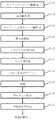
図1は、実施の形態1における半導体装置の製造方法の要部を表すフローチャートである。図1において、実施の形態1の半導体装置の製造方法では、エッチングストッパ膜形成工程(S102)と、low−k膜形成工程(S104)と、ポロジェン含有キャップ膜形成工程(S106)と、開口部形成工程(S110)と、バリアメタル膜形成工程(S112)と、シード膜形成工程(S114)と、めっき及びアニール工程(S116)と、研磨工程(S118)と、ポロジェン除去工程(S120)と、拡散防止膜形成工程(S122)という一連の工程を実施する。
The first embodiment will be described below with reference to the drawings.
FIG. 1 is a flowchart showing the main part of the semiconductor device manufacturing method according to the first embodiment. 1, in the manufacturing method of the semiconductor device of the first embodiment, an etching stopper film forming step (S102), a low-k film forming step (S104), a porogen-containing cap film forming step (S106), an opening Forming step (S110), barrier metal film forming step (S112), seed film forming step (S114), plating and annealing step (S116), polishing step (S118), porogen removal step (S120), A series of steps called diffusion preventing film forming step (S122) is performed.
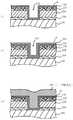
図2は、図1のフローチャートに対応して実施される工程を表す工程断面図である。図2では、図1のエッチングストッパ膜形成工程(S102)から開口部形成工程(S110)までを示している。 FIG. 2 is a process sectional view showing a process performed corresponding to the flowchart of FIG. FIG. 2 shows the etching stopper film forming step (S102) to the opening forming step (S110) in FIG.
図2(a)において、エッチングストッパ膜形成工程(S102)として、基板200上に、化学気相成長(CVD)法によってエッチングストッパ膜210を例えば20〜40nmの膜厚で形成する。エッチングストッパ膜の材料として、例えば、炭窒化シリコン(SiCN)、炭化シリコン(SiC)、或いは多孔質ではない炭酸化シリコン(denseSiCO)等が好適である。形成方法は、CVD法に限るものではなくその他の方法で成膜しても構わない。また、基板200として、例えば、直径300ミリのシリコンウェハを用いる。ここでは、コンタクトプラグ層やデバイス部分等の図示は省略している。そして、基板200上には、その他の金属配線またはヴィアプラグ等、図示しない各種の半導体素子あるいは構造を有する層が形成されていても構わない。或いは、その他の層が形成されていても構わない。 In FIG. 2A, as an etching stopper film formation step (S102), an
図2(b)において、low−k膜形成工程(S104)として、エッチングストッパ膜210上に、多孔質の低誘電率絶縁材料を用いたlow−k膜220を例えば100nmの厚さで形成する。low−k膜220を形成することで、比誘電率kが2.4〜3.0程度の絶縁膜を得ることができる。low−k膜220は、1層分の配線層の層間絶縁膜における主たる絶縁膜となる。ここでは、一例として、CVD法を用いて比誘電率が2.5未満の低誘電率絶縁材料となる多孔質のSiOCH膜を形成する。形成方法は、CVD法に限るものではなく、例えば、溶液をスピンコートし熱処理して薄膜を形成するSOD(spin on dielectric coating)法を用いても好適である。SOD法で形成するlow−k膜220の材料としては、例えば、多孔質のメチルシルセスキオキサン(methyl silsesquioxane:MSQ)を用いることができる。また、MSQの他に、例えば、ポリメチルシロキサン、ポリシロキサン、ハイドロジェンシロセスキオキサンなどのシロキサン骨格を有する膜、ポリアリーレンエーテル、ポリベンゾオキサゾール、ポリベンゾシクロブテンなどの有機樹脂を主成分とする膜、および多孔質シリカ膜などのポーラス膜からなる群から選択される少なくとも一種を用いて形成しても構わない。かかるlow−k膜220の材料では、比誘電率が2.5未満の低誘電率を得ることができる。SOD法では、例えば、スピナーで成膜し、このウエハをホットプレート上で窒素雰囲気中でのベークを行った後、最終的にホットプレート上で窒素雰囲気中ベーク温度よりも高温でキュアを行なうことにより形成することができる。low−k材料や形成条件などを適宜調節することにより、所定の物性値を有する多孔質の絶縁膜が得られる。 In FIG. 2B, as a low-k film forming step (S104), a low-
図2(c)において、ポロジェン含有キャップ膜形成工程(S106)として、low−k膜220上に、ポロジェン成分10を含有する材料を用いてキャップ膜230を例えば20〜40nmの厚さで形成する。例えば、CVD法を用いてキャップ膜230を形成する。キャップ膜230は、膜厚が、low−k膜220よりも薄く形成される。キャップ膜230の材料としては、ポロジェン成分10を含有すると共に、水素を含む炭酸化シリコン(SiOCH)が好適である。ポロジェン成分10としては、例えば、炭素(C)と水素(H)を含有するポリマー、一例として、C10H16等が好適である。2C, as the porogen-containing cap film forming step (S106), the
形成方法として、例えば、メチルジエトキシシラン(Methyl−di−ethoxy−silane)、アルファターピネン(alpha−terpinene:C10H16)、酸素(O2)、ヘリウム(He)からなる混合ガスを図示しないチャンバ内に流入し、チャンバ内の圧力を例えば1.3×10³Pa(10Torr)以下に維持した状態で、low−k膜220が成膜された基板200を例えば250℃に加熱し、チャンバ内の下部電極及び上部電極に高周波電力を供給し、プラズマを発生させる。メチルジエトキシシランは主骨格成分形成用のガスであり、アルファターピネンはポロジェン成分形成用ガスである。これにより、low−k膜220上に有機シロキサンを主骨格成分とするSiOCH膜によるキャップ膜230が形成される。このとき、混合ガスに含まれるアルファターピネンがプラズマによって重合し、有機高分子が形成される。この有機高分子がポロジェン成分10であり、SiOCH膜中に均一に取り込まれる。As a forming method, for example, a mixed gas composed of methyldiethoxysilane (Methyl-di-ethoxy-silane), alpha-terpinene (alpha-terpinene: C10 H16 ), oxygen (O2 ), and helium (He) is illustrated. The
なお、主骨格成分形成用の有機シリコンガスとしては、ジメチルシラン(Di−Methyl−Silane)、トリメチルシラン(Tri−Methyl−Silane)、テトラメチルシラン(Tetra−Methyl−Silane)、ジメチルフェニルシラン(Di−Methyl−Phenyl−Silane)、トリメチルシリルアセチレン(Tri−Methyl−Silyl−Acetylene)、モノメチルジエトキシシラン(Mono−Methyl−Di−Ethoxy−Silane)、ジメチルジエトキシシラン(Di−Methyl−Di−Ethoxy−Silane)、テトラメチルシクロテトラシロキサン(Tetra−Methyl−Cyclo−Tetra−Siloxane)、及びオクタメチルシクロテトラシロキサン(Octa−Methyl−Cyclo−Tetra−Siloxane)の少なくとも1つを用いることができる。 The organic silicon gas for forming the main skeleton component includes dimethylsilane (Di-Methyl-Silane), trimethylsilane (Tri-Methyl-Silane), tetramethylsilane (Tetra-Methyl-Silane), dimethylphenylsilane (Di). -Methyl-Phenyl-Silane), Trimethylsilylacetylene (Tri-Methyl-Sylyl-Acetylene), Monomethyldiethoxysilane (Mono-Methyl-Di-Ethoxy-Silane), Dimethyldiethoxysilane (Di-Methyl-Di-Ethylene) ), Tetramethylcyclotetrasiloxane (Tetra-Methyl-Cyclo-Tetra-Siloxane), and octame It is possible to use at least one of Le cyclotetrasiloxane (Octa-Methyl-Cyclo-Tetra-Siloxane).
一方、ポロジェン成分形成用ガスとしては、メタン(Methane)、エチレン(Ethylene)、プロピレン(Propylene)、アルファターピネン(Alpha−Terpinene)、ガンマターピネン(Gamma−Terpinene)、及びリモーネン(Limonene)の少なくとも1つを用いることができる。 On the other hand, as the porogen component forming gas, at least methane, ethylene, propylene, alpha-terpine, gamma-terpinene, and limonene are included. One can be used.
また、ここでは、CVD法でSiOCH膜を形成しているが、形成方法はこれに限るものではない。例えば、ポロジェン材料を含有する溶液をスピンコートし熱処理して薄膜を形成するSOD法を用いても好適である。SOD法で形成する低誘電率のキャップ膜230の材料としては、例えば、MSQを用いることができる。また、MSQの他に、例えば、ポリメチルシロキサン、ポリシロキサン、ハイドロジェンシロセスキオキサンなどのシロキサン骨格を有する膜、ポリアリーレンエーテル、ポリベンゾオキサゾール、ポリベンゾシクロブテンなどの有機樹脂を主成分とする膜、および多孔質シリカ膜などのポーラス膜からなる群から選択される少なくとも一種を用いて形成しても構わない。SOD法では、例えば、スピナーで成膜し、このウエハをホットプレート上で窒素雰囲気中でのベークを行なうことでポロジェン成分10が均一に含有された例えば有機シロキサンを主骨格成分とするSiOCH膜のキャップ膜230を形成することができる。いずれの低誘電率絶縁膜の材料を用いても、最終的に、比誘電率kがlow−k膜220よりも低い、例えば2.0以下の低誘電率を得ることができる。 Here, the SiOCH film is formed by the CVD method, but the forming method is not limited to this. For example, the SOD method in which a thin film is formed by spin-coating a solution containing a porogen material and performing heat treatment is also suitable. As a material of the low dielectric
実施の形態1では、キャップ膜230中のポロジェン成分10を膜形成後直ちには除去せずに、ここでは主骨格形成を行うに留める。例えば、low−k膜220上にCVD法或いはSOD法により膜を形成した後、200〜300℃で加熱処理を行うことで主骨格を形成することができる。かかる状態では、ポロジェン成分10が残ったままで除去されていないので膜中にポア(空孔)が形成されておらず、膜が緻密な状態となっており、そのため機械的強度もlow−k膜220のようなポーラス膜に比べて強い状態を維持することができる。 In the first embodiment, the
図2(d)において、開口部形成工程(S110)として、図示しないレジストパターンをマスクとして、露出したキャップ膜230とその下層のlow−k膜220を異方性エッチング法により実質的に同じ幅で続けてエッチングすることにより、配線溝或いはヴィアホールとなる開口部150を形成する。その際、エッチングストッパ膜210をエッチングストッパとしてエッチングする。その後、エッチングストッパ膜210をエッチングして、基板200まで届くように開口部150を形成する。異方性エッチング法により除去することで、基板200の表面に対し、略垂直に開口部150を形成することができる。例えば、一例として、反応性イオンエッチング(RIE)法により開口部150を形成すればよい。エッチングの際、機械的強度の強いキャップ膜230がlow−k膜220のマスクとなるのでlow−k膜220を保護することができる。 In FIG. 2D, as the opening forming step (S110), the exposed
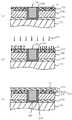
図3は、図1のフローチャートに対応して実施される工程を表す工程断面図である。図3では、図1のバリアメタル膜形成工程(S112)からめっき及びアニール工程(S116)までを示している。 FIG. 3 is a process sectional view showing a process performed corresponding to the flowchart of FIG. FIG. 3 shows from the barrier metal film forming step (S112) to the plating and annealing step (S116) in FIG.
図3(a)において、バリアメタル膜形成工程(S112)として、エッチングにより形成された開口部150内面上及びキャップ膜230表面上に導電性材料の一例となるバリアメタル材料を用いたバリアメタル膜240を形成する。スパッタ法を用いるスパッタリング装置内でTaN膜を例えば膜厚5nm堆積し、バリアメタル膜240を形成する。バリアメタル材料の堆積方法としては、PVD法に限らず、原子層気相成長(atomic layer deposition:ALD、あるいは、atomic layer chemical vapor deposition:ALCVD)法やCVD法などを用いることができる。PVD法を用いる場合より被覆率を良くすることができる。バリアメタル膜240の材料としては、TaNの他、タンタル(Ta)、チタン(Ti)、ルテニウム(Ru)、タングステン(W)、ジルコニウム(Zr)、アルミニウム(Al)、ニオブ(Nb)等の金属、窒化チタン(TiN)、窒化タングステン(WN)等に代表されるこれらの金属の窒化物、或いはこれらの金属を含有するその他の材料を単独でまたは積層して用いることができる。 In FIG. 3A, as a barrier metal film forming step (S112), a barrier metal film using a barrier metal material as an example of a conductive material on the inner surface of the
図3(b)において、シード膜形成工程(S114)として、スパッタ等の物理気相成長(PVD)法により、次の工程である電解めっき工程のカソード極となるCu薄膜をシード膜250としてバリアメタル膜240が形成された開口部150内壁及び基板200表面に堆積(形成)させる。 In FIG. 3B, as a seed film formation step (S114), a Cu thin film serving as a cathode electrode in the next electrolytic plating step is used as a
図3(c)において、めっき及びアニール工程(S116)として、シード膜250をカソード極として、電解めっき等の電気化学成長法により導電性材料の一例となるCu膜260をシード膜250が形成された開口部150及び基板200表面に堆積させる。ここでは、例えば、膜厚200nmのCu膜260を堆積させ、堆積させた後にアニール処理を例えば250℃の温度で30分間行なう。 In FIG. 3C, as a plating and annealing step (S116), the
図4は、図1のフローチャートに対応して実施される工程を表す工程断面図である。図4では、図1の研磨工程(S118)から拡散防止膜形成工程(S122)までを示している。 FIG. 4 is a process sectional view showing a process performed corresponding to the flowchart of FIG. FIG. 4 shows from the polishing step (S118) to the diffusion prevention film forming step (S122) in FIG.
図4(a)において、研磨工程(S118)として、CMP法によって、基板200の表面を研磨して、開口部以外に表面に堆積した配線層となるシード膜250を含むCu膜260とバリアメタル膜240を研磨除去する。その結果、図4(a)に示すように、Cu膜260の表面とキャップ膜230の表面とが同一面となるように平坦化される。以上によりCu配線を形成することができる。研磨の際、機械的強度の強いキャップ膜230がlow−k膜220上に形成されているのでlow−k膜220を保護することができる。 In FIG. 4A, as the polishing step (S118), the surface of the
ここで、図4(a)に示す状態では、キャップ膜230中にポロジェン成分10が残ったままの状態であり、比誘電率kがlow−k膜220に比べて高い状態なので、ポロジェン成分10を次の工程で除去する。 Here, in the state shown in FIG. 4A, the
図4(b)において、ポロジェン除去工程(S120)として、表面が露出したキャップ膜230中からポロジェン成分10を除去する。ポロジェン成分10は、例えば電子線(EB)照射によるキュアを行って除去する。具体的には、キャップ膜230の表面が露出した基板200を図示しないチャンバ内部で例えば1.3×10³Pa(10Torr)以下に維持した状態で、例えば350〜400℃に加熱する。次に、このチャンバ内部にアルゴン(Ar)ガスを流入し、チャンバ内部の圧力を一定に維持する。圧力が一定になった後、電子線170をキャップ膜230に照射する。例えば、加速エネルギーが10〜20keVの条件で電子線170を照射する。電子線照射により気泡となったポロジェン成分10を除去することで、キャップ膜230中にポア12が形成される。これにより、low−k膜220よりも低い、例えば2.0以下の比誘電率kを有する、全体に均一なポア12が散りばめられた多孔質のキャップ膜230を得ることができる。言い換えると、ポロジェン成分10を除去することで、例えば、キャップ膜230とlow−k膜220とが同じSiOCH膜であれば、キャップ膜230の密度が、low−k膜220の密度よりも小さくなる。例えば、密度が1.2〜1.4g/cm3のlow−k膜220に対して、密度が1.0〜1.2g/cm3のキャップ膜230を形成することができる。In FIG. 4B, as the porogen removal step (S120), the
或いは、電子線照射の代わりに紫外線照射によるキュアを行ってポロジェン成分10の除去を行っても好適である。具体的には、キャップ膜230の表面が露出した基板200を図示しないチャンバ内部で例えば1.3×10³Pa(10Torr)以下に維持した状態で、例えば350〜400℃に加熱する。次に、このチャンバ内部にArガスを流入し、チャンバ内部の圧力を一定に維持する。圧力が一定になった後、紫外線をキャップ膜230に照射する。ここでは、例えば200nmから300nmの波長領域を持つ紫外線をキャップ膜230に照射する。これにより、ポロジェン成分10が気泡となって除去される。これにより、low−k膜220よりも低い、例えば2.0以下の比誘電率を有する、全体に均一なポア12が散りばめられた多孔質のキャップ膜230(ポーラスSiOCH膜)を得ることができる。同様に、例えば、キャップ膜230とlow−k膜220とが同じSiOCH膜であれば、キャップ膜230の密度が、low−k膜220の密度よりも小さくなる。例えば、密度が1.2〜1.4g/cm3のlow−k膜220に対して、密度が1.0〜1.2g/cm3のキャップ膜230を形成することができる。Alternatively, the
また、キャップ膜230中からポロジェン成分10を除去する際、low−k膜220ではポロジェン成分は存在しないので、キャップ膜230中からポロジェン成分10を除去する際にlow−k膜220の膜収縮が起こらない。このように、実施の形態1では、low−k膜220、キャップ膜230をともに多孔質に形成する場合でもlow−k膜220の膜収縮のリスクを回避できる。 Further, when the
図4(c)において、拡散防止膜形成工程(S122)として、CVD法を用いて、キャップ膜230のポア12の一部を残しながら、一部がキャップ膜230中に食い込むように、キャップ膜230上にCuの拡散を防止する拡散防止膜270(バリア膜)を形成する。例えば、キャップ膜230上に20〜40nmの膜厚で形成する。拡散防止膜270の材料として、例えば、炭窒化シリコン(SiCN)、炭化シリコン(SiC)、或いは多孔質ではない炭酸化シリコン(denseSiCO)等が好適である。また、形成方法は、CVD法に限るものではなくその他の方法で成膜しても構わない。拡散防止膜270は、上層のCu配線層、ヴィアプラグ層、或いは上層のCu配線とヴィアプラグを一体で形成するデュアルダマシン配線層を形成する場合に、かかる上層の層間絶縁膜に開口部を形成する際のエッチングストッパ膜としても機能する。 In FIG. 4C, as the diffusion prevention film forming step (S122), the cap film is formed using the CVD method so that a part of the
図5は、実施の形態1における拡散防止膜がキャップ膜に食い込んだ状態を示す概念図である。図5に示すように、キャップ膜230には、ポロジェン10が揮発する際の通路となるガス抜き穴14やポロジェン10が含有されていた位置にポア12が形成される。すなわち、キャップ膜230の表面全体には均一にガス抜き穴14が空いている。拡散防止膜270は、その一部がキャップ膜230の表面全体に空いたガス抜き穴14やその下のポア12に食い込むように形成される。例えば、キャップ膜230の表面に空いたガス抜き穴14のサイズが2〜4nmの場合に、拡散防止膜270を形成する際のCVDガスのサイズは1nm以下となり、ガス抜き穴14に進入することができる。 FIG. 5 is a conceptual diagram showing a state in which the diffusion preventing film in the first embodiment bites into the cap film. As shown in FIG. 5, pores 12 are formed in the
ここで、拡散防止膜270がキャップ膜230に食い込む食い込み領域20の深さdは、キャップ膜230の全面に均一に食い込み領域20が形成可能な深さであって、キャップ膜230の比誘電率kが主たる絶縁膜となるlow−k膜220の比誘電率kを超えない範囲とするとよい。例えば、5〜10nm食い込むように形成されると好適である。食い込み深さdは、例えば、拡散防止膜270をPE−CVD法で形成する場合、バイアス電圧等を調整することで制御することができる。或いは、例えば、拡散防止膜270をCVD法で形成する場合、使用するプロセスガスの分子量で調整しても好適である。或いは、キャップ膜230に含有させておくポロジェン成分10の量で調整してもよい。通常、ポロジェン成分10は、複数の分子が一体となってキャップ膜230中に分散している。そのため、ポロジェン成分10の量を少なくすれば形成されるポア12のサイズやガス抜き穴14のサイズも小さくなるのでガスの進入を抑制することができる。よって、食い込み深さを浅くすることができる。逆に、ポロジェン成分10の量を増やせば形成されるポア12のサイズやガス抜き穴14のサイズも大きくなるのでガスの進入を促進することができる。よって、食い込み深さを深くすることができる。或いは、キャップ膜230に含有させておくポロジェン成分10の分散率で調整してもよい。 Here, the depth d of the biting
以上のようにして、low−k膜220より比誘電率kが低いキャップ膜230とlow−k膜220とがCu配線となるCu膜260の側面に位置するように配置された図4(c)に示すような一層分のCu配線層を形成することができる。 As described above, the
図6は、実施の形態1におけるキャップ膜の比誘電率と、拡散防止膜とキャップ膜との界面での電界強度との関係をシミュレーションした結果を示す図である。図6において、縦軸は拡散防止膜270とキャップ膜230との界面での電界強度、横軸はキャップ膜230の比誘電率を示している。また、電界強度の値は二次元の電磁界シミュレータを用いた。前提として、low−k膜220の比誘電率kを2.7、拡散防止膜270の比誘電率kを3.7とし、Cu配線間の70nm幅の絶縁膜スペースに1Vの電位差を掛けた場合を示している。シミュレーションした結果、図6に示すように、キャップ膜230の比誘電率kを小さくすることで、それに応じて界面の電界強度も弱まることがわかる。 FIG. 6 is a diagram showing a result of simulating the relationship between the relative dielectric constant of the cap film and the electric field strength at the interface between the diffusion prevention film and the cap film in the first embodiment. In FIG. 6, the vertical axis represents the electric field strength at the interface between the
図7は、実施の形態1におけるキャップ膜の比誘電率と、TDDB寿命との関係を示す予測図である。図7において、縦軸はTDDB寿命、横軸はキャップ膜230の比誘電率を示している。図6での評価と同様の条件では、キャップ膜230の比誘電率kが2の場合、比誘電率kが4の場合の約7倍の長寿命化を見積もることができる。理由としては、図6で示した電界強度の緩和が以下に説明するようにCuイオンのドリフト量を減らしたためと考えられる。 FIG. 7 is a prediction diagram showing the relationship between the relative dielectric constant of the cap film and the TDDB lifetime in the first embodiment. In FIG. 7, the vertical axis represents the TDDB life, and the horizontal axis represents the relative dielectric constant of the
図8は、実施の形態1のキャップ膜と従来のキャップ膜とにおける電界強度とCuドリフトとの関係を示す概念図である。従来のキャップ膜231は、low−k膜220の比誘電率k1よりも十分大きい比誘電率k2を有していた。かかる場合、図8(a)に示すように、Cu膜260で示す2つのCu配線間では、比誘電率が大きいキャップ膜231、特に、その上部、すなわち、Cu配線上端部において、相対的に電界30が密となり、最も電界強度が大きくなる。そのため、Cu配線上端部において、Cuイオンのドリフトが生じやすくなる。これに対し、実施の形態1のキャップ膜230は、low−k膜220の比誘電率k1よりも小さい比誘電率k2を有している。かかる場合、図8(b)に示すように、Cu膜260で示す2つのCu配線間では、電界30が分散され、Cu配線上端部において、相対的に電界30が疎となり、電界強度が小さくなる。そのため、Cu配線上端部において、Cuイオンのドリフトを抑制することができる。また、Cu配線の上端部以外は、バリアメタル膜240で側面側および底面側が覆われており、元々Cuイオンのドリフトが生じにくい。 FIG. 8 is a conceptual diagram showing the relationship between electric field strength and Cu drift in the cap film of the first embodiment and the conventional cap film. The
以上のように、キャップ膜230の比誘電率k2をlow−k膜220の比誘電率k1よりも小さくすることで、Cuイオンのドリフトを抑制することができる。その結果、TDDB寿命の長寿命化を図ることができる。 As described above, by making the relative permittivity k2 of the
図9は、実施の形態1における拡散防止膜の食い込みの有無によるCuドリフトの様子を比較した概念断面図である。仮に、拡散防止膜270がキャップ膜230に食い込まずに、拡散防止膜270とキャップ膜230との界面が図9(a)に示すように平面のみであった場合、2つのCu膜260による配線間において、電界強度が大きく生じればCuイオンのドリフトが生じることになる。これに対し、実施の形態1では、拡散防止膜270がキャップ膜230に食い込んでいるので、図9(b)に示すように、電界強度が大きくCuイオンがドリフトを起こす場合でも、食い込み箇所が進行の障害となり、隣のCu配線まで到達しにくくなる。このように、拡散防止膜270の一部をキャップ膜230に食い込ませて界面を平面ではなくすことでCuイオンのドリフトを抑制することができる。 FIG. 9 is a conceptual cross-sectional view comparing the state of Cu drift depending on the presence or absence of biting of the diffusion barrier film in the first embodiment. If the
実施の形態1では、キャップ膜230の比誘電率k2をlow−k膜220の比誘電率k1よりも小さくすることに加えて、さらに、拡散防止膜270の一部をキャップ膜230に食い込ませて界面を平面ではなくすことで、Cuイオンのドリフトをより抑制することができる。 In the first embodiment, in addition to making the relative dielectric constant k2 of the
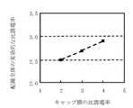
図10は、実施の形態1におけるキャップ膜の比誘電率と、配線層一層分全体での実効的な比誘電率との関係をシミュレーションした結果を示す図である。図10において、縦軸は配線層全体での実効的な比誘電率、横軸はキャップ膜230の比誘電率を示している。実効誘電率は二次元電磁界シミュレーションにより求めた。ここでも前提として、low−k膜220の比誘電率kを2.7、拡散防止膜270の比誘電率kを3.7とし、配線部分と絶縁部分とが140nmピッチの密集配線構造の線間容量を計算して結果を求めた。その結果、図10に示すように、キャップ膜230を低誘電率化することにより、実効誘電率の低減を図ることができる。 FIG. 10 is a diagram showing a result of simulating the relationship between the relative dielectric constant of the cap film in
以上のように、実施の形態1では、キャップ膜230の比誘電率k2をlow−k膜220の比誘電率k1よりも小さくすることで、配線層全体として、従来よりもさらなる低誘電率化を図ることができる。 As described above, in the first embodiment, the relative dielectric constant k2 of the
実施の形態2.
実施の形態1では、ポア12やガス抜き穴14によってポーラスな状態になったキャップ膜230上に拡散防止膜270を形成することで拡散防止膜270の一部を食い込ませる構成について説明した。しかし、キャップ膜230は、ポーラス膜に限るものではない。実施の形態2では、ポーラス膜ではないキャップ膜の場合について説明する。
In the first embodiment, the configuration in which a part of the
図11は、実施の形態2における半導体装置の製造方法の要部を表すフローチャートである。図11において、実施の形態2の半導体装置の製造方法では、ポロジェン含有キャップ膜形成工程(S106)の代わりに、低誘電率キャップ膜形成工程(S108)を加えた点と、ポロジェン除去工程(S120)が無くなった点以外は、図1と同様である。エッチングストッパ膜形成工程(S102)からlow−k膜形成工程(S104)までの各工程の内容は、実施の形態1と同様である。 FIG. 11 is a flowchart showing a main part of the method of manufacturing a semiconductor device in the second embodiment. 11, in the method for manufacturing the semiconductor device according to the second embodiment, a low dielectric constant cap film forming step (S108) is added instead of the porogen-containing cap film forming step (S106), and the porogen removing step (S120). 1 is the same as FIG. The contents of each process from the etching stopper film forming process (S102) to the low-k film forming process (S104) are the same as those in the first embodiment.
図12は、図11のフローチャートに対応して実施される工程を表す工程断面図である。図12では、図11の低誘電率キャップ膜形成工程(S108)から開口部形成工程(S110)までと拡散防止膜形成工程(S122)とを示している。 FIG. 12 is a process sectional view showing a process performed corresponding to the flowchart of FIG. FIG. 12 shows the low dielectric constant cap film forming step (S108) to the opening forming step (S110) and the diffusion preventing film forming step (S122) of FIG.
図12(a)において、低誘電率キャップ膜形成工程(S108)として、low−k膜220上に、低誘電率材料を用いてキャップ膜232を例えば20〜40nmの厚さで形成する。例えば、SOD法を用いてキャップ膜232を形成する。キャップ膜232は、膜厚が、low−k膜220よりも薄く形成される。キャップ膜232の材料としては、後工程としてポロジェン除去の必要がなく、内部にポアが無くとも比誘電率がlow−k膜220よりも低い材料が用いられる。上述したSiOCH系ではなく、例えば、炭素(C)を含有するポリマー材料が好適である。例えば、フッ化炭素(CF)を含むポリマー材料がより好適である。かかる材料により、low−k膜220よりも比誘電率が低い、比誘電率kが、1.5〜2.0の低誘電率キャップ膜232を得ることができる。形成方法は、SOD法に限らず、CVD法を用いても構わない。 In FIG. 12A, as a low dielectric constant cap film forming step (S108), a
図12(b)において、開口部形成工程(S110)として、図示しないレジストパターンをマスクとして、露出したキャップ膜232とその下層のlow−k膜220を異方性エッチング法により選択的にエッチングして、配線溝或いはヴィアホールとなる開口部150を形成する。その際、エッチングストッパ膜210をエッチングストッパとしてエッチングする。その後、エッチングストッパ膜210をエッチングして、基板200まで届くように開口部150を形成する。その他の内容は、実施の形態1と同様である。例えば、一例として、RIE法により開口部150を形成する場合には、バイアス電圧等を調整することで、機械的強度が弱いキャップ膜232とその下のlow−k膜220を保護すればよい。その後のバリアメタル膜形成工程(S112)から研磨工程(S118)までの各工程は、実施の形態1と同様である。研磨工程(S118)の際には、研磨荷重やスラリの調整により機械的強度が弱いキャップ膜232を保護すればよい。 In FIG. 12B, as the opening forming step (S110), the exposed
図12(c)において、拡散防止膜形成工程(S122)として、CVD法を用いて、キャップ膜232上にCuの拡散を防止する拡散防止膜270(バリア膜)を形成する。例えば、キャップ膜232上に20〜40nmの膜厚で形成する。ここでは、キャップ膜232にポアが存在しないので、拡散防止膜270がキャップ膜232中に食い込まずにキャップ膜232上に堆積することになる。その他の内容は、実施の形態1と同様である。 In FIG. 12C, as the diffusion preventing film forming step (S122), a diffusion preventing film 270 (barrier film) for preventing the diffusion of Cu is formed on the
以上のようにして、キャップ膜232の比誘電率k2をlow−k膜220の比誘電率k1よりも小さくした一層分の配線層を形成することができる。かかる場合でも図6〜8で説明したように、Cuイオンのドリフトを抑制することができる。その結果、TDDB寿命の長寿命化を図ることができる。また、図10で説明したように、かかるCu配線層全体でのさらなる低誘電率化を図ることができる。 As described above, it is possible to form a single wiring layer in which the relative dielectric constant k2 of the
以上の説明において、上記各実施の形態における配線層の材料として、Cu以外に、Cu−Sn合金、Cu−Ti合金、Cu−Al合金等の、半導体産業で用いられるCuを主成分とする材料を用いても同様の効果が得られる。 In the above description, as a material for the wiring layer in each of the above embodiments, in addition to Cu, a material mainly composed of Cu used in the semiconductor industry, such as a Cu—Sn alloy, a Cu—Ti alloy, and a Cu—Al alloy. The same effect can be obtained by using.
以上、具体例を参照しつつ実施の形態について説明した。しかし、本発明は、これらの具体例に限定されるものではない。例えば、上述した例では、シングルダマシン法により一層分の配線層を形成する場合について説明したが、デュアルダマシン法により配線とヴィアプラグとを同時に形成する場合の主たる絶縁膜となるlow−k膜と配線上部側面側に位置することになるキャップ膜とについても同様に成り立つ。また、デュアルダマシン法でのキャップ膜とその上に形成される拡散防止膜とについても同様に成り立つ。 The embodiments have been described above with reference to specific examples. However, the present invention is not limited to these specific examples. For example, in the above-described example, the case where the wiring layer for one layer is formed by the single damascene method has been described. However, the low-k film serving as a main insulating film when the wiring and the via plug are simultaneously formed by the dual damascene method. The same holds true for the cap film located on the side of the upper side of the wiring. The same holds true for the cap film in the dual damascene method and the diffusion prevention film formed thereon.
さらに、層間絶縁膜の膜厚や、開口部のサイズ、形状、数などについても、半導体集積回路や各種の半導体素子において必要とされるものを適宜選択して用いることができる。 Further, the film thickness of the interlayer insulating film and the size, shape, number, and the like of the opening can be appropriately selected from those required in the semiconductor integrated circuit and various semiconductor elements.
その他、本発明の要素を具備し、当業者が適宜設計変更しうる全ての半導体装置及び半導体装置の製造方法は、本発明の範囲に包含される。 In addition, all semiconductor devices and methods of manufacturing a semiconductor device that include elements of the present invention and that can be appropriately modified by those skilled in the art are included in the scope of the present invention.
また、説明の簡便化のために、半導体産業で通常用いられる手法、例えば、フォトリソグラフィプロセス、処理前後のクリーニング等は省略しているが、それらの手法が含まれ得ることは言うまでもない。 Further, for the sake of simplicity of explanation, techniques usually used in the semiconductor industry, such as a photolithography process, cleaning before and after processing, are omitted, but it goes without saying that these techniques may be included.
10 ポロジェン成分、12 ポア、14 ガス抜き穴、150 開口部、170 電子線、200 基板、220 low−k膜、230,231,232 キャップ膜、240 バリアメタル膜、260 Cu膜、270 拡散防止膜10 Porogen component, 12 pores, 14 vent holes, 150 openings, 170 electron beam, 200 substrate, 220 low-k film, 230, 231 and 232 cap film, 240 barrier metal film, 260 Cu film, 270 anti-diffusion film
Claims (5)
Translated fromJapanese前記絶縁膜上に、ポアが形成されるキャップ膜を形成する工程と、
前記キャップ膜と前記絶縁膜に開口部を形成する工程と、
前記開口部内に導電性材料を堆積させる工程と、
前記開口部内に前記導電性材料が堆積させられた後に、前記ポアの一部を残しながら一部が前記キャップ膜中に食い込むように、前記キャップ膜上に前記導電性材料の拡散を防止する拡散防止膜を形成する工程と、
を備えたことを特徴とする半導体装置の製造方法。Forming an insulating film on the substrate;
Forming a cap film on which the pores are formed on the insulating film;
Forming an opening in the cap film and the insulating film;
Depositing a conductive material in the opening;
Diffusion for preventing diffusion of the conductive material on the cap film such that after the conductive material is deposited in the opening, a part of the pore remains in the cap film while leaving a part of the pore. Forming a prevention film;
A method for manufacturing a semiconductor device, comprising:
前記開口部内に前記導電性材料が堆積させられた後であって前記拡散防止膜が形成される前に、前記キャップ膜中から前記ポロジェン成分を除去する工程をさらに備えたことを特徴とする請求項1記載の半導体装置の製造方法。When forming the cap film, using a material containing a porogen component, the cap film is formed so as to leave the porogen component,
The method further comprises the step of removing the porogen component from the cap film after the conductive material is deposited in the opening and before the diffusion prevention film is formed. Item 14. A method for manufacturing a semiconductor device according to Item 1.
前記絶縁膜上に、ポロジェン成分を含有する材料を用いて前記ポロジェン成分を残すようにキャップ膜を形成する工程と、
前記キャップ膜と前記絶縁膜に開口部を形成する工程と、
前記開口部内に導電性材料を堆積させる工程と、
前記開口部内に前記導電性材料が堆積させられた後に、前記キャップ膜中から前記ポロジェン成分を除去して前記絶縁膜よりも低い比誘電率を有する多孔質のキャップ膜を得る工程と、
を備えたことを特徴とする半導体装置の製造方法。Forming an insulating film on the substrate;
Forming a cap film on the insulating film so as to leave the porogen component using a material containing a porogen component;
Forming an opening in the cap film and the insulating film;
Depositing a conductive material in the opening;
After the conductive material is deposited in the opening, removing the porogen component from the cap film to obtain a porous cap film having a relative dielectric constant lower than that of the insulating film;
A method for manufacturing a semiconductor device, comprising:
前記絶縁膜上に形成された、前記絶縁膜の比誘電率よりも低い比誘電率のキャップ膜と、
前記キャップ膜と前記絶縁膜とが側面に位置するように配置された配線と、
を備えたことを特徴とする半導体装置。An insulating film formed on the substrate;
A cap film having a dielectric constant lower than the dielectric constant of the insulating film formed on the insulating film;
Wiring arranged so that the cap film and the insulating film are located on side surfaces;
A semiconductor device comprising:
Priority Applications (2)
| Application Number | Priority Date | Filing Date | Title |
|---|---|---|---|
| JP2008273818AJP2010103329A (en) | 2008-10-24 | 2008-10-24 | Method of manufacturing semiconductor device, and semiconductor device |
| US12/537,759US20100102452A1 (en) | 2008-10-24 | 2009-08-07 | Method for fabricating semiconductor device and semiconductor device |
Applications Claiming Priority (1)
| Application Number | Priority Date | Filing Date | Title |
|---|---|---|---|
| JP2008273818AJP2010103329A (en) | 2008-10-24 | 2008-10-24 | Method of manufacturing semiconductor device, and semiconductor device |
Publications (1)
| Publication Number | Publication Date |
|---|---|
| JP2010103329Atrue JP2010103329A (en) | 2010-05-06 |
Family
ID=42116680
Family Applications (1)
| Application Number | Title | Priority Date | Filing Date |
|---|---|---|---|
| JP2008273818APendingJP2010103329A (en) | 2008-10-24 | 2008-10-24 | Method of manufacturing semiconductor device, and semiconductor device |
Country Status (2)
| Country | Link |
|---|---|
| US (1) | US20100102452A1 (en) |
| JP (1) | JP2010103329A (en) |
Families Citing this family (13)
| Publication number | Priority date | Publication date | Assignee | Title |
|---|---|---|---|---|
| JP2011129690A (en)* | 2009-12-17 | 2011-06-30 | Toshiba Corp | Method for manufacturing semiconductor device and semiconductor device |
| US8889544B2 (en)* | 2011-02-16 | 2014-11-18 | Taiwan Semiconductor Manufacturing Company, Ltd. | Dielectric protection layer as a chemical-mechanical polishing stop layer |
| US9330989B2 (en)* | 2012-09-28 | 2016-05-03 | Taiwan Semiconductor Manufacturing Company, Ltd. | System and method for chemical-mechanical planarization of a metal layer |
| KR101998788B1 (en) | 2013-04-22 | 2019-07-11 | 삼성전자주식회사 | Semiconductor Devices and Methods of Fabricating the Same |
| US9142451B2 (en)* | 2013-09-16 | 2015-09-22 | Globalfoundries Inc. | Reduced capacitance interlayer structures and fabrication methods |
| US9406615B2 (en)* | 2013-12-24 | 2016-08-02 | Intel Corporation | Techniques for forming interconnects in porous dielectric materials |
| US9117822B1 (en)* | 2014-04-29 | 2015-08-25 | Globalfoundries Inc. | Methods and structures for back end of line integration |
| US10886250B2 (en) | 2015-07-10 | 2021-01-05 | Invensas Corporation | Structures and methods for low temperature bonding using nanoparticles |
| US9633971B2 (en) | 2015-07-10 | 2017-04-25 | Invensas Corporation | Structures and methods for low temperature bonding using nanoparticles |
| US10699897B2 (en)* | 2016-01-24 | 2020-06-30 | Applied Materials, Inc. | Acetylide-based silicon precursors and their use as ALD/CVD precursors |
| TWI822659B (en) | 2016-10-27 | 2023-11-21 | 美商艾德亞半導體科技有限責任公司 | Structures and methods for low temperature bonding |
| CN108231659B (en) | 2016-12-15 | 2020-07-07 | 中芯国际集成电路制造(北京)有限公司 | Interconnect structure and method of making the same |
| JP2024501559A (en) | 2020-12-30 | 2024-01-12 | アデイア セミコンダクター ボンディング テクノロジーズ インコーポレイテッド | Structures with conductive features and methods of forming the same |
Family Cites Families (9)
| Publication number | Priority date | Publication date | Assignee | Title |
|---|---|---|---|---|
| US6124164A (en)* | 1998-09-17 | 2000-09-26 | Micron Technology, Inc. | Method of making integrated capacitor incorporating high K dielectric |
| US6165891A (en)* | 1999-11-22 | 2000-12-26 | Chartered Semiconductor Manufacturing Ltd. | Damascene structure with reduced capacitance using a carbon nitride, boron nitride, or boron carbon nitride passivation layer, etch stop layer, and/or cap layer |
| US6924222B2 (en)* | 2002-11-21 | 2005-08-02 | Intel Corporation | Formation of interconnect structures by removing sacrificial material with supercritical carbon dioxide |
| JP3910973B2 (en)* | 2004-04-22 | 2007-04-25 | 株式会社東芝 | Manufacturing method of semiconductor device |
| US7015150B2 (en)* | 2004-05-26 | 2006-03-21 | International Business Machines Corporation | Exposed pore sealing post patterning |
| US7217648B2 (en)* | 2004-12-22 | 2007-05-15 | Taiwan Semiconductor Manufacturing Company, Ltd. | Post-ESL porogen burn-out for copper ELK integration |
| US20070173070A1 (en)* | 2006-01-26 | 2007-07-26 | Mei-Ling Chen | Porous low-k dielectric film and fabrication method thereof |
| US7947579B2 (en)* | 2006-02-13 | 2011-05-24 | Stc.Unm | Method of making dense, conformal, ultra-thin cap layers for nanoporous low-k ILD by plasma assisted atomic layer deposition |
| CN101589459A (en)* | 2007-01-26 | 2009-11-25 | 应用材料股份有限公司 | Uv curing of pecvd-deposited sacrificial polymer films for air-gap ild |
- 2008
- 2008-10-24JPJP2008273818Apatent/JP2010103329A/enactivePending
- 2009
- 2009-08-07USUS12/537,759patent/US20100102452A1/ennot_activeAbandoned
Also Published As
| Publication number | Publication date |
|---|---|
| US20100102452A1 (en) | 2010-04-29 |
Similar Documents
| Publication | Publication Date | Title |
|---|---|---|
| JP2010103329A (en) | Method of manufacturing semiconductor device, and semiconductor device | |
| US7439185B2 (en) | Method for fabricating semiconductor device and semiconductor device | |
| CN1276499C (en) | Structural reinforcement of highly porous low k dielectric films by cu diffusion barrier structures | |
| US7816253B2 (en) | Surface treatment of inter-layer dielectric | |
| US7301107B2 (en) | Semiconductor device having reduced intra-level and inter-level capacitance | |
| US9177858B1 (en) | Methods for fabricating integrated circuits including barrier layers for interconnect structures | |
| US7795142B2 (en) | Method for fabricating a semiconductor device | |
| US9059259B2 (en) | Hard mask for back-end-of-line (BEOL) interconnect structure | |
| US6984581B2 (en) | Structural reinforcement of highly porous low k dielectric films by ILD posts | |
| US8878364B2 (en) | Method for fabricating semiconductor device and semiconductor device | |
| KR101077711B1 (en) | Method for fabricating a semiconductor device | |
| JP2005203568A (en) | Fabrication process of semiconductor device, and semiconductor device | |
| JP4698813B2 (en) | Semiconductor device and manufacturing method thereof | |
| JP2005340460A (en) | Process for forming semiconductor device | |
| JP4447433B2 (en) | Semiconductor device manufacturing method and semiconductor device | |
| JP2010165760A (en) | Semiconductor device and method for manufacturing the semiconductor device | |
| JP2005340601A (en) | Process for fabricating semiconductor device and semiconductor device | |
| JP2011142169A (en) | Semiconductor device and manufacturing method thereof | |
| JP2008010630A (en) | Semiconductor device and manufacturing method thereof | |
| JP2005079116A (en) | Method for manufacturing semiconductor device | |
| JP2006060011A (en) | Manufacturing method of semiconductor device | |
| JP2006319116A (en) | Semiconductor device and its manufacturing method | |
| JP2006049534A (en) | Semiconductor device and manufacturing method thereof | |
| JP2011086824A (en) | Method for forming low dielectric constant film and semiconductor device | |
| JP2011155074A (en) | Manufacturing method of semiconductor device |