JP2010098157A - Process of fabricating semiconductor device - Google Patents
Process of fabricating semiconductor deviceDownload PDFInfo
- Publication number
- JP2010098157A JP2010098157AJP2008268326AJP2008268326AJP2010098157AJP 2010098157 AJP2010098157 AJP 2010098157AJP 2008268326 AJP2008268326 AJP 2008268326AJP 2008268326 AJP2008268326 AJP 2008268326AJP 2010098157 AJP2010098157 AJP 2010098157A
- Authority
- JP
- Japan
- Prior art keywords
- gate
- gate portion
- semiconductor device
- active region
- region
- Prior art date
- Legal status (The legal status is an assumption and is not a legal conclusion. Google has not performed a legal analysis and makes no representation as to the accuracy of the status listed.)
- Pending
Links
- 239000004065semiconductorSubstances0.000titleclaimsabstractdescription33
- 238000000034methodMethods0.000titleclaimsabstractdescription14
- 229910021420polycrystalline siliconInorganic materials0.000claimsabstractdescription30
- 229920005591polysiliconPolymers0.000claimsabstractdescription30
- 229910052751metalInorganic materials0.000claimsabstractdescription27
- 239000002184metalSubstances0.000claimsabstractdescription27
- 238000002955isolationMethods0.000claimsabstractdescription23
- 238000005498polishingMethods0.000claimsabstractdescription7
- 238000004519manufacturing processMethods0.000claimsdescription27
- 239000000758substrateSubstances0.000claimsdescription5
- XUIMIQQOPSSXEZ-UHFFFAOYSA-NSiliconChemical compound[Si]XUIMIQQOPSSXEZ-UHFFFAOYSA-N0.000claims1
- 229910052710siliconInorganic materials0.000claims1
- 239000010703siliconSubstances0.000claims1
- 239000010410layerSubstances0.000description9
- ATJFFYVFTNAWJD-UHFFFAOYSA-NTinChemical compound[Sn]ATJFFYVFTNAWJD-UHFFFAOYSA-N0.000description7
- 230000001133accelerationEffects0.000description6
- 230000000694effectsEffects0.000description4
- 239000007769metal materialSubstances0.000description4
- ZOXJGFHDIHLPTG-UHFFFAOYSA-NBoronChemical compound[B]ZOXJGFHDIHLPTG-UHFFFAOYSA-N0.000description3
- 229910052796boronInorganic materials0.000description3
- 238000002513implantationMethods0.000description3
- 229910052785arsenicInorganic materials0.000description2
- RQNWIZPPADIBDY-UHFFFAOYSA-Narsenic atomChemical compound[As]RQNWIZPPADIBDY-UHFFFAOYSA-N0.000description2
- 238000010586diagramMethods0.000description2
- 238000005530etchingMethods0.000description2
- 239000011229interlayerSubstances0.000description2
- 238000001039wet etchingMethods0.000description2
- OKTJSMMVPCPJKN-UHFFFAOYSA-NCarbonChemical compound[C]OKTJSMMVPCPJKN-UHFFFAOYSA-N0.000description1
- 229910004129HfSiOInorganic materials0.000description1
- OAICVXFJPJFONN-UHFFFAOYSA-NPhosphorusChemical compound[P]OAICVXFJPJFONN-UHFFFAOYSA-N0.000description1
- 229910004298SiO 2Inorganic materials0.000description1
- 229910052799carbonInorganic materials0.000description1
- 238000007796conventional methodMethods0.000description1
- 238000000151depositionMethods0.000description1
- 238000009792diffusion processMethods0.000description1
- 150000002739metalsChemical class0.000description1
- 230000003647oxidationEffects0.000description1
- 238000007254oxidation reactionMethods0.000description1
- 230000000149penetrating effectEffects0.000description1
- 229910052698phosphorusInorganic materials0.000description1
- 239000011574phosphorusSubstances0.000description1
- 238000007517polishing processMethods0.000description1
- 229910052814silicon oxideInorganic materials0.000description1
- 239000002002slurrySubstances0.000description1
- 125000006850spacer groupChemical group0.000description1
Images


Landscapes
- Metal-Oxide And Bipolar Metal-Oxide Semiconductor Integrated Circuits (AREA)
- Insulated Gate Type Field-Effect Transistor (AREA)
- Electrodes Of Semiconductors (AREA)
- Element Separation (AREA)
Abstract
Description
Translated fromJapanese本発明は、半導体装置の製造方法に関する。 The present invention relates to a method for manufacturing a semiconductor device.
従来技術として、ダミーゲートをマスクとしてあらかじめ拡散層や配線を作成し、ダミーゲートを除去してメタルゲートを生成するゲートラストと呼ばれる方法がある。ゲートラストプロセスにおいては、ソース/ドレインを先に形成するためにゲートへの熱負荷が小さく、ゲートメタル材料の自由度が高い。 As a conventional technique, there is a method called gate last in which a diffusion layer or wiring is created in advance using a dummy gate as a mask, and the dummy gate is removed to generate a metal gate. In the gate last process, since the source / drain is formed first, the thermal load on the gate is small, and the degree of freedom of the gate metal material is high.
特許文献1には、ダマシーン工程を適用したゲート製造方法について、フィールド領域と活性領域の段差による、均一でない厚さのポリワードラインが形成される問題について、高選択比を有するCMP用スラリを用いて表面が波形をなすように研磨する方法が示されている。 Patent Document 1 uses a CMP slurry having a high selection ratio for the problem of forming a polyword line having a non-uniform thickness due to a step between a field region and an active region in a gate manufacturing method using a damascene process. A method of polishing so that the surface is corrugated is shown.
特許文献2には、フルシリサイド化されたゲート電極を有する半導体装置の製造方法において、活性領域と素子分離領域との段差による影響を受けることなく、活性領域上と素子分離領域上とに形成されたそれぞれのゲート電極形成膜及びゲート配線形成膜の露出を精度良く行う方法が示されている。 In
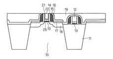
しかしながら、ゲートラストプロセスで作製するトランジスタにおいて、ポリシリコンを抜くため、層間絶縁膜(PMD)19をデポした後に図17のようにCMPを行うが、このCMPの終点はそのゲートの高さで決まるため、活性領域10と素子分離領域11の高さがばらつきによって異なる場合、活性領域10上と素子分離領域11上とにゲートがあると、図18のようにゲートのポリシリコンを抜くことができない可能性がある。最終的な構造としては、素子分離領域11が低いと図19のように素子分離領域11上のゲートはポリシリコン12となり、活性領域10上はメタル22となってしまう。逆に素子分離領域11が高いと、素子分離領域11上のゲートがメタルとなり、活性領域10上はポリシリコンとなってしまう。このため、ゲートの抵抗がレイアウトによって変わってしまい、抵抗のばらつきが生じる問題があった。 However, in a transistor manufactured by the gate last process, CMP is performed as shown in FIG. 17 after depositing the interlayer insulating film (PMD) 19 in order to remove polysilicon. The end point of this CMP is determined by the height of the gate. Therefore, in the case where the heights of the
特許文献1は、ゲートの頭を出すために層間膜がうねった構成になっており、メタルの露光やエッチングが困難になる問題がある。また、特許文献2は、ゲートラストに関するものではない。 Patent Document 1 has a structure in which an interlayer film is undulated in order to bring out the head of a gate, and there is a problem that it is difficult to expose and etch a metal. Further,
本発明は、上記の問題を解決するためになされたもので、ゲートラストプロセスで作製するトランジスタにおいて、活性領域と素子分離領域の高さばらつきのためゲートのポリシリコンを抜くことができないことにより、ゲートの抵抗にばらつきが生じるのを防ぐことを目的とする。 The present invention has been made to solve the above problem, and in a transistor manufactured by the gate last process, the gate polysilicon cannot be removed due to the height variation of the active region and the element isolation region. The purpose is to prevent variations in gate resistance.
本発明の一実施形態に係る半導体装置の製造方法は、半導体基板に活性領域と前記活性領域を囲み前記活性領域に対して上面高さが異なる素子分離領域とを形成する工程、活性領域の上に第1のポリシリコン膜を有する第1のゲート部を形成すると共に、素子分離領域の上に第1のゲート部と上面高さが異なる第2のポリシリコン膜を有する第2のゲート部を形成する工程を備える。その後、第1のゲート部及び第2のゲート部を覆う絶縁膜を形成する工程、第1のゲート部及び第2のゲート部の上面が共に露出するように、絶縁膜及び第1のゲート部又は第2のゲート部の一部を研磨除去する工程、露出された部分より、第1のポリシリコン膜及び第2のポリシリコン膜を抜く工程、第1のゲート部及び第2のゲート部を覆うメタルを形成する工程を備える。その後、第1のゲート部及び第2のゲート部の上面が共に露出するようにメタルを研磨除去し、第1のゲート部と第2のゲート部で厚みの異なるメタルを残す工程を備えて構成される。 A method of manufacturing a semiconductor device according to an embodiment of the present invention includes a step of forming an active region and an element isolation region surrounding the active region and having a top surface different from the active region on a semiconductor substrate, Forming a first gate portion having a first polysilicon film and a second gate portion having a second polysilicon film having a top surface height different from that of the first gate portion on the element isolation region. Forming. Thereafter, a step of forming an insulating film covering the first gate portion and the second gate portion, and the insulating film and the first gate portion so that the upper surfaces of the first gate portion and the second gate portion are exposed. Alternatively, a step of polishing and removing a part of the second gate portion, a step of removing the first polysilicon film and the second polysilicon film from the exposed portion, the first gate portion and the second gate portion A step of forming a covering metal; Thereafter, the metal is polished and removed so that the upper surfaces of the first gate portion and the second gate portion are both exposed, and the first gate portion and the second gate portion are left with different thicknesses. Is done.
本発明の一実施形態に係る半導体装置の製造方法は、活性領域上の第1のゲート部と、活性領域に対して上面高さが異なる素子分離領域上の第2のゲート部の上面が共に露出するように、第1のゲート部又は第2のゲート部の一部を研磨除去する。そのため、両領域のポリシリコン膜を抜くことができ、第1のゲート部と第2のゲート部で厚みの異なるメタルを残すことが可能である。従って、ゲートの抵抗がレイアウトによって変わる問題を解決することができ、また研磨後の表面は平坦なため、メタルの露光やエッチングが容易である。 In the method of manufacturing a semiconductor device according to an embodiment of the present invention, the first gate portion on the active region and the upper surface of the second gate portion on the element isolation region having a different upper surface height from the active region are both A part of the first gate portion or the second gate portion is polished and removed so as to be exposed. Therefore, the polysilicon film in both regions can be removed, and it is possible to leave metals having different thicknesses in the first gate portion and the second gate portion. Therefore, the problem that the resistance of the gate varies depending on the layout can be solved, and the polished surface is flat, so that the metal exposure and etching are easy.
以下、この発明をその実施の形態を示す図面に基づいて具体的に説明する。 Hereinafter, the present invention will be specifically described with reference to the drawings showing embodiments thereof.
<実施の形態1>
(構成)
図1に、本実施の形態に係るNMOSトランジスタの断面図を示す。この図では、半導体基板に活性領域10と活性領域10を囲み活性領域10に対して上面高さが異なる素子分離領域11が形成されている。<Embodiment 1>
(Constitution)
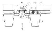
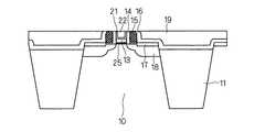
FIG. 1 is a cross-sectional view of an NMOS transistor according to this embodiment. In this figure, an
活性領域10の表面にはゲート絶縁膜25を介してTiN層13が形成され、TiN層13の上部にはTi、TiN等による仕事関数調整用の調整膜21が形成され、調整膜21の上部にはメタル層22が形成される。上述したTiN層13、調整膜21、メタル層22によりゲート電極が形成され、ゲート電極の側面を覆うように下側サイドウォール14、上側サイドウォール15が形成される。調整膜21は、メタル層22および下側サイドウォール14の間にも形成される。 A
ゲート電極を挟む活性領域10の主面にはLDD領域17、LDD領域17の外側にはn型のソース/ドレイン領域18が形成され、nMOSトランジスタが形成される。分離領域11の表面においても、上述したLDD領域17およびソース/ドレイン領域18以外については、同様にnMOSトランジスタが形成される。ただし、素子分離領域11上のNMOSトランジスタのゲート、サイドウォールの高さは、活性領域10上のものと比べて高くなっている。 An
上側サイドウォール15の側面、活性領域10上および素子分離領域11上には酸化膜16が形成され、酸化膜16の上部にはPMD19が形成される。さらに全体を覆うようにPMD23が形成される。LDD領域17の上面には、PMD19,23を貫通するコンタクト24が形成される。 An
なお、図1には図示していないが、PMOSトランジスタ側についても、NMOSトランジスタ側と同様にゲート絶縁膜を介して形成されたゲート電極、サイドウォール、LDD領域、ソース/ドレイン領域が形成され、pMOSトランジスタが形成される。
(製法)
次に、図2〜図15を用いて、本実施の形態に係る半導体装置の製法について説明する。図2〜図7は、NMOSトランジスタ、PMOSトランジスタについて併用した図である。Although not shown in FIG. 1, the gate electrode, the sidewall, the LDD region, and the source / drain region formed through the gate insulating film are formed on the PMOS transistor side as well as the NMOS transistor side. A pMOS transistor is formed.
(Manufacturing method)
Next, a method for manufacturing the semiconductor device according to the present embodiment will be described with reference to FIGS. 2 to 7 are diagrams in which NMOS transistors and PMOS transistors are used together.
図2に示すように、半導体基板に活性領域10と活性領域10を囲み活性領域10に対して上面高さが異なる素子分離領域11とを形成する。 As shown in FIG. 2, an
半導体基板にウェルを形成し、チャネルドープを行う。Nウェル領域については、ボロンを加速電圧が数十keV、ドーズ量が数e13cm-2で印加し、Pウェル領域については、リンを数百keV、ドーズ量が数e13cm-2で印加する。A well is formed in a semiconductor substrate and channel doping is performed. For the N well region, boron is applied at an acceleration voltage of several tens of keV and a dose of several e13 cm−2 , and for the P well region, phosphorus is applied at a few hundred keV and a dose of several e13 cm−2 .
次に、図3に示すように、ゲート酸化を行いSiO2/HfSiO2からなる酸化膜25を形成し、その後TiN層13、ポリシリコン12を成膜し、ゲートをパターニングする。酸化膜25はSiON/HfSiONでもよい。すなわち、活性領域10の上にポリシリコン12(第1のポリシリコン膜)を有する第1のゲート部30を形成すると共に、素子分離領域11の上にポリシリコン12(第2のポリシリコン膜)を有する第2のゲート部31を形成する。さらにオフセットスペーサを形成した後、PMOSトランジスタ領域のみ、炭素を加速電圧が数keV〜数十keV、ドーズ量が数e14〜15cm-2で注入する。Next, as shown in FIG. 3, gate oxidation is performed to form an
その後、図4に示すようにソースドレイン注入を行い、ソース/ドレイン領域18を形成する。nMOSでは砒素を加速電圧が数十keV、ドーズ量が数e15cm-2、pMOSではボロンを加速電圧が数keV、ドーズ量が数e15cm-2で注入を行う。さらに、LDD注入を行いLDD領域17を形成する。(nMOS:砒素 加速電圧は数keV、ドーズ量は数e14〜15cm-2、pMOS:ボロン 加速電圧は数百eV、ドーズ量は数e14〜15cm-2)。LDD注入が終わった後、下側サイドウォール14、上側サイドウォール15からなる、サイドウォールを形成する。Thereafter, source / drain implantation is performed as shown in FIG. 4 to form source /
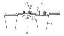
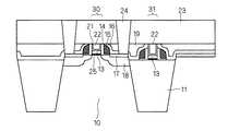
次いで、図5に示すように、SiN16を数nm、PMD19を数百nmデポする。すなわち、第1のゲート部30及び第2のゲート部31を覆う絶縁膜を形成する。その後、図6に示すようにCMPを行い、さらに図7に示すようにポリシリコン12をウェットエッチングで除去する。すなわち、第1のゲート部30及び第2のゲート部31の上面が共に露出するように、絶縁膜及び第1のゲート部30の一部を研磨除去し、露出された部分より、ポリシリコン12(第1のポリシリコン膜及び第2のポリシリコン膜)を抜く。 Next, as shown in FIG. 5, SiN 16 is deposited by several nm and
図8〜図10は、その後のNMOSトランジスタにおける製造工程を示す。まず、PMOS用仕事関数調整メタル材料20をデポする。すなわち、第1のゲート部30及び第2のゲート部31を覆うメタル20を形成する。Ta、Tanなどを用いる。 8 to 10 show subsequent manufacturing steps in the NMOS transistor. First, the work function adjusting
その後、PMOSトランジスタ領域にレジストを形成し、図9に示すようにNMOSトランジスタ領域のPMOS用仕事関数調整メタル材料20を除去する。さらに、図10に示すようにNMOS用仕事関数調整メタル21を成膜する。Ti、TiN等をデポする。 Thereafter, a resist is formed in the PMOS transistor region, and the PMOS work function adjusting
この時点で、PMOSトランジスタ領域では図11に示すような構成になる。図12〜図15は、NMOSトランジスタ、PMOSトランジスタについて併用した図である。その後、図12に示すように、AL、またはWなどのメタル22をデポする。その後メタル22のCMPを行い、図13に示す構成となる。すなわち、第1のゲート部30及び第2のゲート部31の上面が共に露出するようにメタル22を研磨除去し、図13に示すように第1のゲート部30と第2のゲート部31で厚みの異なるメタル22を残す。 At this point, the PMOS transistor region has a configuration as shown in FIG. 12 to 15 are diagrams in which NMOS transistors and PMOS transistors are used together. Thereafter, as shown in FIG. 12, the
その後、図14に示すように全体を覆うようにPMD23をデポし、さらに図15に示すようにLDD17上にコンタクト24を形成する。 After that, the
(効果)
図6に示すように、活性領域10上の第1のゲート部30と、活性領域10に対して上面高さが異なる素子分離領域11上の第2のゲート部31の上面が共に露出するように、第1のゲート部30の一部を研磨除去する。そのため、両領域のポリシリコン膜12を抜くことができ、第1のゲート部30と第2のゲート部31で厚みの異なるメタル22を残すことが可能である。従って、ゲートの抵抗がレイアウトによって変わる問題を解決することができ、また図6に示すように研磨後の表面は平坦なため、メタル22の露光やエッチングが容易である。(effect)
As shown in FIG. 6, both the
<実施の形態2>
(構成)
図16に、本実施の形態に係るNMOSトランジスタの断面図を示す。この図では、実施の形態1で示した図15と比較して、下側サイドウォール14、上側サイドウォール15,(以降、下側サイドウォール14と上側サイドウォール15を合わせて、サイドウォール14,15とする。)の高さが低く形成されている。その他の構成は実施の形態1と同様であるので、ここでの詳細な説明は省略する。<
(Constitution)
FIG. 16 shows a cross-sectional view of the NMOS transistor according to the present embodiment. In this figure, compared with FIG. 15 shown in Embodiment 1, the
(製法)
本実施の形態においては、実施の形態の図4で示した工程において、サイドウォール14,15は、ゲート厚よりも低い状態で形成される。その後は、実施の形態1の図5〜図7に示したように、サイドウォール14,15およびゲートを覆うようにSiN16を数nm、PMD19を数百nmデポし、どちらもポリシリコン12が露出されるまでCMPを行い、ポリシリコン12をウェットエッチングで抜く。(Manufacturing method)
In the present embodiment, the
その他の製法は実施の形態1と同様であるので、ここでの詳細な説明は省略する。 Since other manufacturing methods are the same as those in the first embodiment, detailed description thereof is omitted here.
(効果)
実施の形態1と同様に、素子分離領域11上、活性領域10上のゲートの高さがそろうようにCMPを行うことで、両領域のポリシリコン12を抜くことができ、共にメタル22を埋め込むことが可能である。このため、ゲートの抵抗がレイアウトによって変わる問題を解決することができる。また、本実施の形態においては、絶縁膜及び第1のゲート部30の一部を研磨除去する際(実施の形態1で示した図5から図6への工程。)、サイドウォール14,15がCMPの研磨レートに影響しないため、CMPの終点判定の精度が高くなる効果がある。(effect)
As in the first embodiment, by performing CMP so that the gate heights on the
10 活性領域、11 LDD領域、12 ポリシリコン、13 TiN層、14 下側サイドウォール、15 上側サイドウォール、16 酸化膜、17 LDD領域、18 ソース/ドレイン領域、19 PMD、20 PMOS用仕事関数調整メタル材料、21 NMOS用仕事関数調整メタル、22 メタル、23 PMD、24 コンタクト、25 ゲート絶縁膜、30 第1のゲート部、31 第2のゲート部。 10 active region, 11 LDD region, 12 polysilicon, 13 TiN layer, 14 lower sidewall, 15 upper sidewall, 16 oxide film, 17 LDD region, 18 source / drain region, 19 PMD, 20 work function adjustment for PMOS Metal material, 21 NMOS work function adjusting metal, 22 metal, 23 PMD, 24 contact, 25 gate insulating film, 30 first gate portion, 31 second gate portion.
Claims (1)
Translated fromJapanese(b)前記活性領域の上に第1のポリシリコン膜を有する第1のゲート部を形成すると共に、前記素子分離領域の上に前記第1のゲート部と上面高さが異なる第2のポリシリコン膜を有する第2のゲート部を形成する工程と、
(c)前記第1のゲート部及び前記第2のゲート部を覆う絶縁膜を形成する工程と、
(d)前記第1のゲート部及び前記第2のゲート部の上面が共に露出するように、前記絶縁膜及び前記第1のゲート部又は前記第2のゲート部の一部を研磨除去する工程と、
(e)前記露出された部分より、前記第1のポリシリコン膜及び前記第2のポリシリコン膜を抜く工程と、
(f)前記第1のゲート部及び第2のゲート部を覆うメタルを形成する工程と、
(g)前記第1のゲート部及び前記第2のゲート部の上面が共に露出するように前記メタルを研磨除去し、前記第1のゲート部と前記第2のゲート部で厚みの異なる前記メタルを残す工程と、を備える、
半導体装置の製造方法。(A) forming an active region on the semiconductor substrate and an element isolation region surrounding the active region and having a top surface different from the active region;
(B) forming a first gate portion having a first polysilicon film on the active region, and a second polysilicon having a top surface height different from that of the first gate portion on the element isolation region; Forming a second gate portion having a silicon film;
(C) forming an insulating film covering the first gate portion and the second gate portion;
(D) Polishing and removing the insulating film and a part of the first gate portion or the second gate portion so that the upper surfaces of the first gate portion and the second gate portion are both exposed. When,
(E) removing the first polysilicon film and the second polysilicon film from the exposed portion;
(F) forming a metal covering the first gate portion and the second gate portion;
(G) The metal is polished and removed so that the upper surfaces of the first gate portion and the second gate portion are exposed, and the first gate portion and the second gate portion have different thicknesses. And a step of leaving
A method for manufacturing a semiconductor device.
Priority Applications (1)
| Application Number | Priority Date | Filing Date | Title |
|---|---|---|---|
| JP2008268326AJP2010098157A (en) | 2008-10-17 | 2008-10-17 | Process of fabricating semiconductor device |
Applications Claiming Priority (1)
| Application Number | Priority Date | Filing Date | Title |
|---|---|---|---|
| JP2008268326AJP2010098157A (en) | 2008-10-17 | 2008-10-17 | Process of fabricating semiconductor device |
Publications (1)
| Publication Number | Publication Date |
|---|---|
| JP2010098157Atrue JP2010098157A (en) | 2010-04-30 |
Family
ID=42259631
Family Applications (1)
| Application Number | Title | Priority Date | Filing Date |
|---|---|---|---|
| JP2008268326APendingJP2010098157A (en) | 2008-10-17 | 2008-10-17 | Process of fabricating semiconductor device |
Country Status (1)
| Country | Link |
|---|---|
| JP (1) | JP2010098157A (en) |
Cited By (4)
| Publication number | Priority date | Publication date | Assignee | Title |
|---|---|---|---|---|
| CN102543705A (en)* | 2011-07-12 | 2012-07-04 | 上海华力微电子有限公司 | Polycrystalline silicon gate electrode integration process for high-pressure devices and low-pressure devices |
| CN102543706A (en)* | 2011-07-22 | 2012-07-04 | 上海华力微电子有限公司 | Integration process for different polycrystalline silicon gate electrode thicknesses |
| KR101188806B1 (en) | 2010-07-14 | 2012-10-12 | 타이완 세미콘덕터 매뉴팩쳐링 컴퍼니 리미티드 | An interconnection structure for n/p metal gates |
| KR20150140195A (en)* | 2014-06-05 | 2015-12-15 | 삼성전자주식회사 | Fabricating method of semiconductor device and the semiconductor device fabricated the method |
- 2008
- 2008-10-17JPJP2008268326Apatent/JP2010098157A/enactivePending
Cited By (6)
| Publication number | Priority date | Publication date | Assignee | Title |
|---|---|---|---|---|
| KR101188806B1 (en) | 2010-07-14 | 2012-10-12 | 타이완 세미콘덕터 매뉴팩쳐링 컴퍼니 리미티드 | An interconnection structure for n/p metal gates |
| CN102543705A (en)* | 2011-07-12 | 2012-07-04 | 上海华力微电子有限公司 | Polycrystalline silicon gate electrode integration process for high-pressure devices and low-pressure devices |
| CN102543706A (en)* | 2011-07-22 | 2012-07-04 | 上海华力微电子有限公司 | Integration process for different polycrystalline silicon gate electrode thicknesses |
| KR20150140195A (en)* | 2014-06-05 | 2015-12-15 | 삼성전자주식회사 | Fabricating method of semiconductor device and the semiconductor device fabricated the method |
| US9385120B2 (en) | 2014-06-05 | 2016-07-05 | Samsung Electronics Co., Ltd. | Semiconductor device and method of fabricating the same |
| KR102172712B1 (en)* | 2014-06-05 | 2020-11-02 | 삼성전자주식회사 | Fabricating method of semiconductor device and the semiconductor device fabricated the method |
Similar Documents
| Publication | Publication Date | Title |
|---|---|---|
| KR101785864B1 (en) | Structure and method for nfet with high k metal gate | |
| US7754593B2 (en) | Semiconductor device and manufacturing method therefor | |
| CN108470733B (en) | Method for manufacturing semiconductor device | |
| TWI524397B (en) | Integrated circuit for replacing metal gate with improved threshold voltage performance and manufacturing method thereof | |
| US8361848B2 (en) | Precise resistor on a semiconductor device | |
| JP4299791B2 (en) | Method for fabricating a gate structure of a CMOS device | |
| US8969922B2 (en) | Field effect transistors and method of forming the same | |
| CN101714507A (en) | Semiconductor device with metal gate stack and method of manufacturing the same | |
| US7495299B2 (en) | Semiconductor device | |
| CN107516649B (en) | Semiconductor device and method of manufacturing the same | |
| CN103165466A (en) | Semiconductor device including polysilicon resistor and metal gate resistor and methods of fabricating thereof | |
| TW201013930A (en) | Novel high-k metal gate structure and method of making | |
| JP2010098157A (en) | Process of fabricating semiconductor device | |
| CN100533692C (en) | Manufacturing method of insulated gate field effect transistor | |
| US20060134874A1 (en) | Manufacture method of MOS semiconductor device having extension and pocket | |
| JP2010010507A (en) | Semiconductor device, and method for manufacturing of the same | |
| JP2005259945A (en) | Semiconductor device and manufacturing method thereof | |
| JP2006086467A (en) | Semiconductor device and manufacturing method thereof | |
| JP2003051552A (en) | Method for manufacturing semiconductor integrated circuit device | |
| JP2006032648A (en) | Semiconductor device manufacturing method including pattern forming method | |
| JP2008117845A (en) | Semiconductor device and manufacturing method thereof | |
| JP2007287793A (en) | Manufacturing method of semiconductor device | |
| JP4546054B2 (en) | Manufacturing method of semiconductor device | |
| JP2009016754A (en) | Semiconductor device and manufacturing method thereof | |
| JP5099087B2 (en) | Manufacturing method of semiconductor device |
Legal Events
| Date | Code | Title | Description |
|---|---|---|---|
| A711 | Notification of change in applicant | Free format text:JAPANESE INTERMEDIATE CODE: A712 Effective date:20100524 |