JP2010097606A - Semiconductor device and wireless tag using the same - Google Patents
Semiconductor device and wireless tag using the sameDownload PDFInfo
- Publication number
- JP2010097606A JP2010097606AJP2009216307AJP2009216307AJP2010097606AJP 2010097606 AJP2010097606 AJP 2010097606AJP 2009216307 AJP2009216307 AJP 2009216307AJP 2009216307 AJP2009216307 AJP 2009216307AJP 2010097606 AJP2010097606 AJP 2010097606A
- Authority
- JP
- Japan
- Prior art keywords
- circuit
- film
- protection circuit
- voltage
- overvoltage protection
- Prior art date
- Legal status (The legal status is an assumption and is not a legal conclusion. Google has not performed a legal analysis and makes no representation as to the accuracy of the status listed.)
- Withdrawn
Links
Images


Classifications
- H—ELECTRICITY
- H10—SEMICONDUCTOR DEVICES; ELECTRIC SOLID-STATE DEVICES NOT OTHERWISE PROVIDED FOR
- H10D—INORGANIC ELECTRIC SEMICONDUCTOR DEVICES
- H10D89/00—Aspects of integrated devices not covered by groups H10D84/00 - H10D88/00
- H10D89/60—Integrated devices comprising arrangements for electrical or thermal protection, e.g. protection circuits against electrostatic discharge [ESD]
- H10D89/601—Integrated devices comprising arrangements for electrical or thermal protection, e.g. protection circuits against electrostatic discharge [ESD] for devices having insulated gate electrodes, e.g. for IGFETs or IGBTs
- G—PHYSICS
- G06—COMPUTING OR CALCULATING; COUNTING
- G06K—GRAPHICAL DATA READING; PRESENTATION OF DATA; RECORD CARRIERS; HANDLING RECORD CARRIERS
- G06K19/00—Record carriers for use with machines and with at least a part designed to carry digital markings
- G06K19/06—Record carriers for use with machines and with at least a part designed to carry digital markings characterised by the kind of the digital marking, e.g. shape, nature, code
- G06K19/067—Record carriers with conductive marks, printed circuits or semiconductor circuit elements, e.g. credit or identity cards also with resonating or responding marks without active components
- G06K19/07—Record carriers with conductive marks, printed circuits or semiconductor circuit elements, e.g. credit or identity cards also with resonating or responding marks without active components with integrated circuit chips
- G06K19/0701—Record carriers with conductive marks, printed circuits or semiconductor circuit elements, e.g. credit or identity cards also with resonating or responding marks without active components with integrated circuit chips at least one of the integrated circuit chips comprising an arrangement for power management
- G06K19/0707—Record carriers with conductive marks, printed circuits or semiconductor circuit elements, e.g. credit or identity cards also with resonating or responding marks without active components with integrated circuit chips at least one of the integrated circuit chips comprising an arrangement for power management the arrangement being capable of collecting energy from external energy sources, e.g. thermocouples, vibration, electromagnetic radiation
- G—PHYSICS
- G06—COMPUTING OR CALCULATING; COUNTING
- G06K—GRAPHICAL DATA READING; PRESENTATION OF DATA; RECORD CARRIERS; HANDLING RECORD CARRIERS
- G06K19/00—Record carriers for use with machines and with at least a part designed to carry digital markings
- G06K19/06—Record carriers for use with machines and with at least a part designed to carry digital markings characterised by the kind of the digital marking, e.g. shape, nature, code
- G06K19/067—Record carriers with conductive marks, printed circuits or semiconductor circuit elements, e.g. credit or identity cards also with resonating or responding marks without active components
- G06K19/07—Record carriers with conductive marks, printed circuits or semiconductor circuit elements, e.g. credit or identity cards also with resonating or responding marks without active components with integrated circuit chips
- G06K19/0701—Record carriers with conductive marks, printed circuits or semiconductor circuit elements, e.g. credit or identity cards also with resonating or responding marks without active components with integrated circuit chips at least one of the integrated circuit chips comprising an arrangement for power management
- G06K19/0712—Record carriers with conductive marks, printed circuits or semiconductor circuit elements, e.g. credit or identity cards also with resonating or responding marks without active components with integrated circuit chips at least one of the integrated circuit chips comprising an arrangement for power management the arrangement being capable of triggering distinct operating modes or functions dependent on the strength of an energy or interrogation field in the proximity of the record carrier
- G—PHYSICS
- G06—COMPUTING OR CALCULATING; COUNTING
- G06K—GRAPHICAL DATA READING; PRESENTATION OF DATA; RECORD CARRIERS; HANDLING RECORD CARRIERS
- G06K19/00—Record carriers for use with machines and with at least a part designed to carry digital markings
- G06K19/06—Record carriers for use with machines and with at least a part designed to carry digital markings characterised by the kind of the digital marking, e.g. shape, nature, code
- G06K19/067—Record carriers with conductive marks, printed circuits or semiconductor circuit elements, e.g. credit or identity cards also with resonating or responding marks without active components
- G06K19/07—Record carriers with conductive marks, printed circuits or semiconductor circuit elements, e.g. credit or identity cards also with resonating or responding marks without active components with integrated circuit chips
- G06K19/0701—Record carriers with conductive marks, printed circuits or semiconductor circuit elements, e.g. credit or identity cards also with resonating or responding marks without active components with integrated circuit chips at least one of the integrated circuit chips comprising an arrangement for power management
- G06K19/0715—Record carriers with conductive marks, printed circuits or semiconductor circuit elements, e.g. credit or identity cards also with resonating or responding marks without active components with integrated circuit chips at least one of the integrated circuit chips comprising an arrangement for power management the arrangement including means to regulate power transfer to the integrated circuit
- G—PHYSICS
- G06—COMPUTING OR CALCULATING; COUNTING
- G06K—GRAPHICAL DATA READING; PRESENTATION OF DATA; RECORD CARRIERS; HANDLING RECORD CARRIERS
- G06K19/00—Record carriers for use with machines and with at least a part designed to carry digital markings
- G06K19/06—Record carriers for use with machines and with at least a part designed to carry digital markings characterised by the kind of the digital marking, e.g. shape, nature, code
- G06K19/067—Record carriers with conductive marks, printed circuits or semiconductor circuit elements, e.g. credit or identity cards also with resonating or responding marks without active components
- G06K19/07—Record carriers with conductive marks, printed circuits or semiconductor circuit elements, e.g. credit or identity cards also with resonating or responding marks without active components with integrated circuit chips
- G06K19/077—Constructional details, e.g. mounting of circuits in the carrier
- G06K19/07749—Constructional details, e.g. mounting of circuits in the carrier the record carrier being capable of non-contact communication, e.g. constructional details of the antenna of a non-contact smart card
Landscapes
- Engineering & Computer Science (AREA)
- Computer Hardware Design (AREA)
- Microelectronics & Electronic Packaging (AREA)
- Physics & Mathematics (AREA)
- General Physics & Mathematics (AREA)
- Theoretical Computer Science (AREA)
- Electromagnetism (AREA)
- Near-Field Transmission Systems (AREA)
- Semiconductor Integrated Circuits (AREA)
- Thin Film Transistor (AREA)
Abstract
Translated fromJapaneseDescription
Translated fromJapanese本発明は、無線通信を用いてデータの送受信を行う無線タグに関する。特に無線通信に於いて大電力を受信した場合に、無線通信回路の破壊、又は回路を構成する素子の劣化、破壊を防止する過電圧保護回路の構成に関する。 The present invention relates to a wireless tag that transmits and receives data using wireless communication. In particular, the present invention relates to a configuration of an overvoltage protection circuit that prevents destruction of a wireless communication circuit or deterioration or destruction of elements constituting the circuit when large power is received in wireless communication.
近年、無線通信を利用した個体識別技術(以下、無線通信システムと表記する)が注目を集めている。特に、無線通信によりデータの送受信を行うデータキャリアとして、RFID(Radio Frequency Identification)技術を利用した無線タグ(以下、カード型、チップ型等の形状を問わず、総称して無線タグと表記する)による個体識別技術が注目を集めている。無線タグは、ICタグ、RFIDタグ、電子タグとも呼ばれる。 In recent years, individual identification technology using wireless communication (hereinafter referred to as a wireless communication system) has attracted attention. In particular, as a data carrier for transmitting and receiving data by wireless communication, a wireless tag using RFID (Radio Frequency Identification) technology (hereinafter collectively referred to as a wireless tag regardless of the shape of card type, chip type, etc.) The individual identification technology by is attracting attention. The wireless tag is also called an IC tag, an RFID tag, or an electronic tag.
無線タグを用いた個体識別技術は、製造、流通の分野において、従来のバーコード管理に代わり、多数多量の物品の管理等に役立てられ始めており、個人認証への応用も進められている。 In the fields of manufacturing and distribution, the individual identification technology using a wireless tag has begun to be used for the management of a large number of articles in place of the conventional bar code management, and its application to personal authentication is also being promoted.
ここで言う無線通信システムとは、リーダ/ライタ(以下、R/Wと表記する)等の送受信機(質問器とも言う)と、無線タグとの間のデータの送受信を無線にて行う通信システムである。このような無線通信においては、R/Wから発せられる搬送波に、送受信すべきデータを重畳してやりとりを行う。 The wireless communication system here refers to a communication system that wirelessly transmits and receives data between a wireless tag and a transceiver (also referred to as an interrogator) such as a reader / writer (hereinafter referred to as R / W). It is. In such wireless communication, exchange is performed by superimposing data to be transmitted and received on a carrier wave emitted from the R / W.
また、無線タグにはR/Wから発せられる搬送波、又は搬送波に変調波を重畳して生成された振幅変調波から、無線タグ内部で駆動用の直流電圧を生成することによって、無線タグ内部の回路の駆動電力を賄うものがあり、このような無線タグは内部にバッテリーを持たない。これは一般にパッシブ型と呼ばれている。一方、無線タグの動作に必要な電力を、無線タグ自身に内蔵されたバッテリーから賄うものは、対してアクティブ型と呼ばれている。 In addition, the wireless tag generates a DC voltage for driving inside the wireless tag from a carrier wave emitted from the R / W or an amplitude-modulated wave generated by superimposing the modulated wave on the carrier wave. Some of them cover the driving power of the circuit, and such a wireless tag does not have a battery inside. This is generally called a passive type. On the other hand, a device that supplies power necessary for the operation of the wireless tag from a battery built in the wireless tag itself is called an active type.
パッシブ型の無線タグは、バッテリーを持たないことから小型軽量化が可能であるという利点を有するが、R/Wから発せられる搬送波を受信することで駆動電力を生成するため、搬送波の受信が十分でないと、回路動作に必要な電力を生成できない。 A passive type wireless tag has an advantage that it can be reduced in size and weight because it does not have a battery. However, since the driving power is generated by receiving the carrier wave generated from the R / W, the reception of the carrier wave is sufficient. Otherwise, the power necessary for circuit operation cannot be generated.
このような無線通信システムを用いてアプリケーションが構築される場合に求められる要素の一つに、最大通信距離が長いことや、特定の領域に多数の無線タグが存在する場合、その全てを認識できる、といったことがある。 One of the elements required when an application is constructed using such a wireless communication system is that the maximum communication distance is long or a large number of wireless tags exist in a specific area, all of which can be recognized. And so on.
両者とも、R/Wの搬送波の電力を大きくすることで実現を図る場合が多い。従って、R/Wのごく近傍に無線タグが存在する場合や、R/W近傍にある無線タグの個数が少ない場合においては、無線タグにおいてかなりの大電力が受信されることになる。 Both of them are often realized by increasing the power of the R / W carrier wave. Accordingly, when a wireless tag exists in the very vicinity of the R / W or when the number of wireless tags in the vicinity of the R / W is small, a considerable amount of power is received by the wireless tag.
無線タグにおいて過剰な電力が供給された場合、内部生成される直流電圧も過剰なものとなるため、無線タグの内部回路に高電圧が印加されることで、内部の素子が破壊される恐れがある。そのため、R/Wの搬送波の電力が大きい無線通信システムの構築が想定される無線タグには、過剰な電力を受信する環境に無線タグが存在する場合に、内部で過剰な電力を生成しないようにする、過電圧保護回路が設けられているものがある。このような無線タグが、以下の特許文献1及び特許文献2に開示されている。 If excessive power is supplied to the wireless tag, the internally generated DC voltage will also be excessive, so that a high voltage is applied to the internal circuit of the wireless tag, possibly destroying the internal elements. is there. For this reason, in a wireless tag for which a radio communication system with a large R / W carrier power is assumed, when a wireless tag exists in an environment where excessive power is received, excessive power is not generated internally. In some cases, an overvoltage protection circuit is provided. Such wireless tags are disclosed in
前述の過電圧保護回路は、R/Wから発せられる搬送波、又は振幅変調波を受信して、無線タグ内部で直流電圧を生成する際、生成されて生ずる電源電圧が過剰なものとならないよう、生成される電源電圧が所望の値に達したところで、それ以上の電源電圧が生成されないように動作する。このような動作の例としては、過剰に生成される電力を逃がすパスが形成されるようにする方法や、アンテナが搬送波を受信しにくくする等の方法が挙げられる。 The above-described overvoltage protection circuit receives a carrier wave generated from the R / W or an amplitude-modulated wave and generates a DC voltage inside the wireless tag so that the generated power supply voltage is not excessive. When the power supply voltage to be reached reaches a desired value, the power supply voltage is not generated. Examples of such an operation include a method of forming a path for escaping excessively generated power, and a method of making it difficult for the antenna to receive a carrier wave.
しかしながら、特に13.56MHz帯の周波数帯を用いる無線通信システムにおいては、搬送波に変調波を重畳する際に、振幅の大きい領域と小さい領域の差が10%程度の変調度を有する振幅変調波を用いて信号の送受信が行われる場合がある。このように変調度が小さい振幅変調波の送受信においては、アンテナ周辺の雑音が信号の送受信精度に大きく影響するが、過電圧保護回路が動作するしきい値に近い受信電力の領域では、過電圧保護回路が動作する、停止する、といった動作を繰り返し、結果として信号に雑音が混入してしまう。これらは過電圧保護回路が、無線タグが送受信する信号に合わせて電圧の抑制量を変化させ、アンテナ端子の信号を打ち消してしまうために起こる現象である。このような雑音は、R/Wと無線タグとの通信エラーの要因となる。 However, particularly in a wireless communication system using a 13.56 MHz frequency band, when a modulated wave is superimposed on a carrier wave, an amplitude-modulated wave having a degree of modulation of about 10% in the difference between a large-amplitude region and a small region is used. Signal transmission / reception may be performed. In transmission / reception of amplitude-modulated waves with such a small modulation factor, noise around the antenna greatly affects signal transmission / reception accuracy, but in the region of received power close to the threshold at which the overvoltage protection circuit operates, the overvoltage protection circuit The operation of stopping and stopping is repeated, and as a result, noise is mixed in the signal. These are phenomena that occur because the overvoltage protection circuit changes the voltage suppression amount in accordance with the signal transmitted and received by the wireless tag and cancels the signal at the antenna terminal. Such noise causes a communication error between the R / W and the wireless tag.
本発明の一態様は、受信される電力の強度が過剰になった場合に、内部の回路に過電圧が印加されることを良好に防止し、かつその動作が送受信される信号に雑音として影響しない構成を有する過電圧保護回路を提供することを課題の一つとする。また、R/Wから発せられる搬送波の電力が大きい無線通信システムにおいて、前述の過電圧保護回路を有し、最大通信距離を縮めることなく、無線タグが大電力を受信する近距離でも内部回路の劣化、破壊を防止し、近傍から最大通信距離までの全領域において、R/Wと無線タグ間で正常かつ安定した無線通信を行うことのできる無線タグを提供することを課題の一つとする。 According to one embodiment of the present invention, when the strength of received power becomes excessive, it is possible to satisfactorily prevent an overvoltage from being applied to an internal circuit, and the operation does not affect signals transmitted and received as noise. An object is to provide an overvoltage protection circuit having a configuration. Further, in a wireless communication system in which the power of the carrier wave generated from the R / W is large, the above-described overvoltage protection circuit is included, and the internal circuit is deteriorated even at a short distance where the wireless tag receives high power without reducing the maximum communication distance. Another object of the present invention is to provide a wireless tag capable of preventing destruction and performing normal and stable wireless communication between the R / W and the wireless tag in the entire region from the vicinity to the maximum communication distance.
前述の課題を解決するために、本発明の一態様においては以下のような手段を講じた。 In order to solve the above-described problems, the following measures are taken in one embodiment of the present invention.
本発明の半導体装置の一態様は、外部から供給される電力の大きさを検知し、検知した電力に応じた電位を出力する電圧検出回路と、前記電圧検出回路から出力される前記電位の最大値に応じた電位を保持する記憶回路と、前記記憶回路に保持された電位に応じて、前記電力の受信部のインピーダンスを変化させる保護回路とを有することを特徴とする。 One embodiment of a semiconductor device according to the present invention includes a voltage detection circuit that detects the magnitude of power supplied from the outside and outputs a potential corresponding to the detected power, and a maximum of the potential output from the voltage detection circuit. And a protection circuit that changes an impedance of the power receiving unit in accordance with the potential held in the storage circuit.
本発明の半導体装置の一態様は、外部から供給される電力の大きさを検知し、検知した電力に応じた電位を出力する電圧検出回路と、前記電圧検出回路から出力される電位の最大値に応じた電位を保持する記憶回路と、前記記憶回路に保持された電位に応じて、前記電力の受信部のインピーダンスを変化させ、前記電力の過剰分を消費あるいは反射させる保護回路とを有することを特徴とする。 One embodiment of a semiconductor device of the present invention is a voltage detection circuit that detects the magnitude of power supplied from the outside and outputs a potential corresponding to the detected power, and a maximum value of the potential output from the voltage detection circuit And a protection circuit that changes the impedance of the power receiving unit according to the potential held in the storage circuit and consumes or reflects the excess power. It is characterized by.
また、前述の前記記憶回路は、リセット端子を有し、前記リセット端子にリセット信号が入力されると、前記記憶回路は、保持した電位をリセットすることを特徴とする。 In addition, the memory circuit described above has a reset terminal, and when a reset signal is input to the reset terminal, the memory circuit resets the held potential.
本発明の半導体装置の一態様と、外部と無線で通信を行う無線通信回路と、前記外部から供給される電力を基に直流電圧を生成する電源回路と、前記生成された直流電圧によって駆動され、データの処理を行う論理回路とを用いて、無線タグを提供することができる。 One aspect of the semiconductor device of the present invention, a wireless communication circuit that performs wireless communication with the outside, a power supply circuit that generates a DC voltage based on the power supplied from the outside, and the generated DC voltage A wireless tag can be provided using a logic circuit that processes data.
本発明の一態様が有する過電圧保護回路は、搬送波、又は振幅変調波を受信し、生成電圧が過電圧保護回路の動作開始電圧近傍にある場合においても、一度過電圧保護回路が動作を開始した後、生成電圧の最大値を記憶回路において保持しておき、前記保持された電圧にしたがって過電圧保護回路が制御される。従って、過電圧保護回路が動作を開始する電圧と、過電圧保護回路が動作を停止する電圧が異なるため、過電圧保護回路が動作を開始するタイミングと、過電圧保護回路が動作を停止するタイミングにヒステリシスを持たせることができる。 The overvoltage protection circuit according to one embodiment of the present invention receives a carrier wave or an amplitude-modulated wave, and even when the generated voltage is in the vicinity of the operation start voltage of the overvoltage protection circuit, once the overvoltage protection circuit starts operating, The maximum value of the generated voltage is held in the storage circuit, and the overvoltage protection circuit is controlled according to the held voltage. Therefore, since the voltage at which the overvoltage protection circuit starts operating is different from the voltage at which the overvoltage protection circuit stops operating, the timing at which the overvoltage protection circuit starts operating and the timing at which the overvoltage protection circuit stops operating have hysteresis. Can be made.
この機能により、過電圧保護回路の動作は、搬送波、又は振幅変調波の受信電力のわずかな振れに対して過敏に反応せず、安定するため、変調信号や復調信号が雑音の影響を受けにくくなる。よって、大電力を出力するR/Wを用いた無線通信システムにおいて、過電圧生成から無線タグ内部の回路を良好に保護し、かつ振幅変調波の変調による電力変動によらず安定して正常な無線通信を行うことができる。 With this function, the operation of the overvoltage protection circuit does not react sensitively to slight fluctuations in the received power of the carrier wave or amplitude-modulated wave, and stabilizes, so the modulated signal and demodulated signal are less susceptible to noise. . Therefore, in a wireless communication system using R / W that outputs a large amount of power, the circuit inside the wireless tag is well protected from overvoltage generation, and stable and normal wireless is achieved regardless of power fluctuations due to modulation of amplitude-modulated waves. Communication can be performed.
本発明の実施の形態について、以下に図面を用いて詳細に説明する。ただし、本発明は以下の説明に限定されず、本発明の趣旨及びその範囲から逸脱することなくその形態及び詳細を様々に変更し適用し得ることは当業者であれば容易に理解される。従って、本発明は以下に示す実施の形態の記載内容に限定して解釈されるものではない。なお、以下に説明する本発明の構成において、同一部分又は同様な機能を有する部分には、異なる図面において同一の符号を共通して用い、繰り返しの説明を省略することがある。 Hereinafter, embodiments of the present invention will be described in detail with reference to the drawings. However, the present invention is not limited to the following description, and it is easily understood by those skilled in the art that the modes and details can be variously changed and applied without departing from the spirit and scope of the present invention. Therefore, the present invention should not be construed as being limited to the description of the embodiments below. Note that in the structures of the present invention described below, the same portions or portions having similar functions are denoted by the same reference numerals in different drawings, and description thereof is not repeated.
(実施の形態1)
本発明の第1の実施形態について、図1を用いて説明する。(Embodiment 1)
A first embodiment of the present invention will be described with reference to FIG.
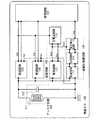
図1は、本発明の一態様にかかる無線タグのブロック図を示しており、無線タグ100は、受信されたデータに基づいて、応答信号を生成するなどといった機能的処理を行う論理回路101と、R/Wと信号の送受信を行うアンテナ回路102と、アンテナ回路102において受信された振幅変調波を復調し、パルス信号を取り出す復調回路103と、論理回路101から出力される応答信号を変調し、R/Wに送信する信号へと変換する変調回路104と、アンテナ回路102において受信された搬送波、又は振幅変調波から直流電圧を生成するための電源回路105と、内部回路に過電圧が印加されるのを防止するための、本発明の一態様にかかる過電圧保護回路106とを有する。アンテナ回路102と、復調回路103と、変調回路104とが、無線通信回路に相当し、無線通信回路を用いることで無線タグ100の外部にあるR/Wと、無線で通信を行うことができる。 FIG. 1 is a block diagram of a wireless tag according to one embodiment of the present invention. The
アンテナ回路102は、アンテナ111及び共振容量112を有する。アンテナ111については、その形状や巻き数によって、R/Wからの搬送波の受信能力が異なるが、特にここでは限定しない。共振容量112は、アンテナ111との組み合わせによって、アンテナ回路102の共振周波数を、R/Wからの搬送波の周波数に最適化するために設けられる容量である。 The
電源回路105は、アンテナ回路102で受信した搬送波、又は振幅変調波を整流し、直流電圧であるエンベローブ電圧Venvを生成するための整流回路113と、Venvが所望の電圧を大きく上回らないように調整し、一定の電圧Vddに調整する定電圧回路114とを有する。 The power supply circuit 105 rectifies the carrier wave or amplitude-modulated wave received by the
過電圧保護回路106は、電源回路105から出力され、論理回路101、復調回路103、変調回路104等の内部回路に供給される電圧を監視する電圧検出回路115と、電圧検出回路115にて検出された電圧の最大値を記憶する記憶回路116と、記憶回路116において記憶された電圧に従って動作する保護回路117とを有する。 The overvoltage protection circuit 106 is detected by a
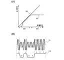
無線タグ100の各部の動作について、図2を用いて説明する。アンテナ回路102において、R/Wからの搬送波、又は振幅変調波を受信すると、整流回路113が交流の搬送波、又は振幅変調波を整流して直流電圧Venv201を生成する。続いて、定電圧回路114はVenv201に基づいたレギュレート電圧Vdd202を出力する。図2(A)に示すように、Venv201が低いとき、すなわち受信電力の小さい領域(203)では、定電圧回路114はほぼVenv=Vddとなるように出力するが、アンテナ回路102における受信電力の上昇に伴ってVenv201が上昇し、ある電圧に達して以降の領域(204)は、Venv201がそれ以上上昇したとしても一定のレギュレート電圧Vdd202を出力する。 The operation of each part of the
一方、復調回路103においては、振幅変調波211を復調して、搬送波に重畳されている信号を取り出し、論理回路101へと入力する(図2(B)参照)。 On the other hand, the
図2(B)に示すように、振幅変調波211は、搬送波の振幅に変調を加えることで信号を重畳している。このような振幅変調波211を復調回路103に入力し、振幅に変調が加えられた領域と加えられていない領域との違いによって、パルス信号212を取り出し、論理回路101に入力する。 As shown in FIG. 2B, the amplitude-modulated
論理回路101においては、パルス信号212に従って応答信号が生成され、変調回路104へと入力される。変調回路104においては、R/Wから出力されている搬送波を、応答信号に従って変調することで、R/Wに応答信号を返信する。 In the
次に、本発明の一態様にかかる過電圧保護回路の構成、及び動作について説明する。図3は、本発明を実施する過電圧保護回路106の回路構成の一例を示したものである。 Next, the structure and operation of the overvoltage protection circuit according to one embodiment of the present invention are described. FIG. 3 shows an example of the circuit configuration of the overvoltage protection circuit 106 embodying the present invention.
整流回路113は、容量301、トランジスタ302、トランジスタ303、及び容量304を有している。図3に示した整流回路113の例では、容量301と、トランジスタ302とで構成されるクランプ回路を有する、半波倍圧整流回路となっている。 The
電圧検出回路115は、抵抗306、トランジスタ307〜トランジスタ310、トランジスタ311、トランジスタ312を有している。 The
記憶回路116は、トランジスタ314、トランジスタ315、容量316を有している。 The
保護回路117は、容量317、及びトランジスタ318を有している。 The
以下、図3に示した過電圧保護回路の詳細な動作について説明する。なお、トランジスタにおいてはNチャネル型、Pチャネル型を双方用いており、各トランジスタのオン、オフを論ずる際には、しきい値電圧を上回る、下回る、と記載するが、特に断りの無い限りは、しきい値電圧を上回るとは、ゲートとソース間の電圧の絶対値が、しきい値電圧の絶対値を上回ることを意味し、しきい値電圧を下回るとは、ゲートとソース間の電圧の絶対値が、しきい値電圧の絶対値を下回ることを意味する。以下、これに従ってNチャネル型トランジスタ、Pチャネル型トランジスタとも同様の記載にて説明する。 The detailed operation of the overvoltage protection circuit shown in FIG. 3 will be described below. It should be noted that both N-channel and P-channel transistors are used, and when discussing on / off of each transistor, it is stated that it exceeds or falls below the threshold voltage, but unless otherwise noted. , Exceeding the threshold voltage means that the absolute value of the voltage between the gate and the source exceeds the absolute value of the threshold voltage, and being below the threshold voltage means that the voltage between the gate and the source Means that the absolute value of is less than the absolute value of the threshold voltage. Hereinafter, N-channel type transistors and P-channel type transistors will be described in the same manner according to this.
アンテナ回路102が搬送波を受信することで共振状態となり、容量301の一方の電極に振幅を与える。容量301の他方の電極には、一方の電極の電位に対し、ダイオード接続されたトランジスタ302のソースとドレイン間に生ずる電圧分だけオフセットされた電位が現れる。さらにダイオード接続されたトランジスタ303によって半波整流され、直流電圧Venvを生成する。容量304は平滑容量であり、生成された直流電圧Venvの保持、及びノイズの平滑化を行う。ここで、抵抗305はプルダウン抵抗であり、整流回路113での直流電圧の生成が行われないとき、整流回路113の出力をVss側にプルダウンする。 When the
生成された直流電圧Venvは、電圧検出回路115にて監視される。具体的には、Venv−Vss間に設けられた抵抗306と、トランジスタ307〜トランジスタ310との間で分圧される電位を取り出す。Venvが低いときには、ダイオード接続されたトランジスタ307〜トランジスタ310の各々においては、ゲートとソース間の電圧がしきい値電圧を下回っているためにオフしており、従ってトランジスタ311のゲートの電位は、Venvにほぼ等しくなり、トランジスタ311はオフする。Venvが上昇すると、トランジスタ307〜トランジスタ310の各々において、ゲートとソース間の電圧がしきい値電圧を上回り、オンする。トランジスタ307〜トランジスタ310の各々におけるソースとドレイン間のインピーダンス変化に従って、トランジスタ311のゲートの電位は、トランジスタ307〜トランジスタ310と抵抗306との間で分圧された電位となる。さらにVenvが上昇すると、トランジスタ311においてゲートとソース間の電圧がしきい値電圧を上回り、オンする。 The generated DC voltage Venv is monitored by the
また、トランジスタ312のゲートにはバイアス電位が印加されており、トランジスタ311がオンしているときには、定電流源として動作している。トランジスタ311のソースとドレイン間のインピーダンス変化に従って、トランジスタ311のドレインの電位は、トランジスタ312のソースとドレイン間の電圧との分圧によって決定される。 In addition, a bias potential is applied to the gate of the
電圧検出回路115からの出力電位は、抵抗313を介して記憶回路116に入力される。なお、抵抗313は、記憶回路116に入力される信号のノイズ低減等のために設けているものであり、特に設けなくても動作原理は変わらない。 The output potential from the
Venvが低いとき、トランジスタ311はオフしており、記憶回路116にはVssに近い電位が入力される。Venvが前述のとおり大きく上昇すると、トランジスタ311がオンして、トランジスタ311及びトランジスタ312で分圧される電位が上昇し、記憶回路116に入力される。容量316の一方の電極は、Vss側に接続されており、他方の電極は、電圧検出回路115の状態によってVssに近い電位、又はトランジスタ311及びトランジスタ312で分圧される電位となって保持される。 When Venv is low, the
容量316の他方の電極の電位が上昇すると、保護回路117においてトランジスタ318のゲートの電位が上昇し、ゲートとソース間の電圧がしきい値電圧を上回るとオンする。このとき、アンテナ回路102の一方の端子は、容量317、トランジスタ318を介してVss側に接続されるため、容量317とトランジスタ318のインピーダンスによって、共振周波数が変化する。 When the potential of the other electrode of the
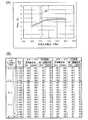
このときの、電圧検出回路115及び保護回路117における、トランジスタ311のゲート電位、トランジスタ318のゲート電位と、Venv変化との関係を、それぞれ図6(A)(B)に模式的に示す。 6A and 6B schematically show the relationship between the gate potential of the
図6(A)において、601は受信電力に対するVenvの変化を示しており、602はトランジスタ311のゲート電位の変化を示している。603で示される電位差が、トランジスタ311のゲートとソース間の電圧に該当する。 In FIG. 6A,
入力電力が小さい領域604においては、トランジスタ307〜トランジスタ310がオフしているため、トランジスタ311のゲートの電位はほぼVenvに等しくなっており、トランジスタ311はオフしている。入力電力が大きい領域605に入ると、トランジスタ307〜トランジスタ310がオンし、603のような電位差が生じ始める。したがってトランジスタ311がオンする。 In the
図6(B)において、606はトランジスタ311のドレイン電位の変化を示している。607で示される電位差が、トランジスタ311のソースとドレイン間の電圧に該当する。 In FIG. 6B,
入力電力が小さい領域604においては、トランジスタ311がオフしているため、トランジスタ311のドレイン電位はほぼVssに等しくなっており、ダイオード接続されたトランジスタ314はオフしている。入力電力が次第に大きくなり、領域609に入ると、トランジスタ311がオンし、トランジスタ311のドレイン電位が上昇を始める。トランジスタ314において、ゲートとソース間の電圧が上昇を始め、しきい値電圧を上回ると、トランジスタ314がオンして、トランジスタ318のゲート電位が上昇を始める。このとき、608で示される電位差が、トランジスタ318のゲートとソース間の電圧に該当する。トランジスタ318のゲートとソース間の電圧がしきい値電圧を上回り、トランジスタ318がオンすると、トランジスタ318のソースとドレイン間のインピーダンスが変化して、電流が流れやすくなる。609の領域では、トランジスタ318は飽和領域で動作しているため、ゲートとソース間の電圧の変化に従ってインピーダンスは大きく変化する。従って、トランジスタ318の消費電流が大きくなり、アンテナ回路102における共振周波数の変化も大きい。さらに入力電力が大きくなり、領域610に入ると、トランジスタ318のゲートとソース間の電圧が拡大し、トランジスタ318は線形領域での動作に入る。この領域では、トランジスタ318は完全にオンし、保護回路117が完全に機能した状態となる。 In the
以上の動作により、過剰な電圧生成が生じた場合、すなわちVenvが過剰に上昇した場合には、保護回路117が動作して、過剰な電力を消費する、または、アンテナの共振周波数を変化させることで反射係数を大きくし、意図的にリターンロスを生じさせることで、整流回路113が生成する電圧を低下させる。 When excessive voltage generation occurs due to the above operation, that is, when Venv increases excessively, the
ここで、記憶回路116においては、容量316の他方の電極の電位、すなわちダイオード接続されたトランジスタ314を介して、トランジスタ318のゲート電位がひとたび上昇すると、ダイオード接続されたトランジスタ314によって逆方向への電流が阻害されるため、Venvが多少下降して、電圧検出回路115から出力される電位が下降しても、ピーク時の電位を保持している。 Here, in the
これにより、R/Wの振幅変調などに起因する、Venvの微小な電位の上昇、下降によって、トランジスタ318が過敏にオン、オフを繰り返すことが無いため、保護回路117は安定する。 As a result, the
やがて通信を終了するとき、トランジスタ315のゲートにリセット信号が入力されてトランジスタ315がオンすると、ダイオード接続されたトランジスタ314及び容量316で保持されていた電荷はトランジスタ315を介して放電され、トランジスタ318のゲート電位は下降する。これにより、保護回路117は動作を停止する。 When the communication is eventually finished and a reset signal is input to the gate of the
なお、トランジスタ315の制御に関しては、他の構成であっても構わない。例えば、通信を終了してR/Wの搬送波が停止した場合、又は無線タグがR/Wとの通信を終了して、応答範囲から外れた場合などには、電源回路での直流電圧の生成が停止するため、Venvが大きく下降する。このVenvの電位をリセット信号の代わりにトランジスタ315のゲートに入力すると、前述の通信終了後の動作によってVenvが下降し、トランジスタ315がオンすることで、容量316にて保持されていた電位がリセットされ、保護回路117の動作が停止する。 Note that other structures may be used for the control of the
以上の動作によって、本発明の一態様にかかる過電圧保護回路は、過電圧保護回路の動作開始電圧と、動作停止電圧とにヒステリシスを持たせることによって、動作開始電圧近傍での動作/非動作の無意味な切り替わりを抑制し、安定して動作させることができる。 With the above operation, the overvoltage protection circuit according to one embodiment of the present invention has hysteresis in the operation start voltage and the operation stop voltage of the overvoltage protection circuit, thereby preventing the operation / non-operation in the vicinity of the operation start voltage. Suppressing meaningful switching and stable operation.
過電圧保護回路が安定して動作することにより、アンテナへのノイズの影響を最小限に抑えることができるため、通信の安定性向上、最大通信距離の向上に大きく寄与する。 Since the overvoltage protection circuit operates stably, the influence of noise on the antenna can be minimized, which greatly contributes to improving the stability of communication and the maximum communication distance.
なお、本発明は、詳細な回路の構成において図3の構成に限定されるものではなく、トランジスタの極性、電源電位の大小関係によって適宜構成が異なっていても良い。例えば電圧検出回路115において、VenvとVssの分圧に用いるトランジスタ307〜トランジスタ310はNチャネル型トランジスタ、トランジスタ311はPチャネル型トランジスタ、保護回路117で用いているトランジスタ318はNチャネル型トランジスタとしているが、トランジスタの極性及び接続関係を逆にしたとしても同様の機能を有する回路構成は容易であるので、当然ながら本発明に含まれるものである。なおその場合は、トランジスタ315が接続される電源電位等も変更することになるが、本発明の機能としては同じである。 Note that the present invention is not limited to the configuration in FIG. 3 in the detailed circuit configuration, and the configuration may be appropriately changed depending on the magnitude of the polarity of the transistor and the power supply potential. For example, in the
(実施の形態2)
本実施の形態では、上記実施の形態で示した半導体装置を得るための一作製方法を説明する。(Embodiment 2)
In this embodiment, one manufacturing method for obtaining the semiconductor device described in the above embodiment will be described.
まず、基板1201の一表面に剥離層1202を形成し、続けて下地となる絶縁膜1203および半導体膜1204(例えば非晶質珪素を含む膜)を形成する(図12(A)参照)。剥離層1202、絶縁膜1203および半導体膜1204は、連続して形成することができる。連続して形成することにより、大気に曝されないため不純物の混入を防ぐことができる。 First, a
基板1201は、ガラス基板、石英基板、金属基板、ステンレス基板、本工程の処理温度に耐えうる耐熱性があるプラスチック基板等を用いるとよい。このような基板であれば、その面積や形状に大きな制限はないため、例えば、1辺が1メートル以上であって、矩形状のものを用いれば、生産性を格段に向上させることができる。このような利点は、円形のシリコン基板を用いる場合と比較すると、大きな優位点である。従って、回路部を大きく形成した場合であっても、シリコン基板を用いる場合と比較して低コスト化を実現することができる。 As the
なお、本工程では、剥離層1202を基板1201の全面に設けているが、必要に応じて、基板1201の全面に剥離層を設けた後に、フォトリソグラフィ法により剥離層1202を選択的に設けてもよい。また、基板1201に接するように剥離層1202を形成しているが、必要に応じて、基板1201に接するように酸化珪素膜、酸化窒化珪素膜、窒化珪素膜、窒化酸化珪素膜等の絶縁膜を形成し、当該絶縁膜に接するように剥離層1202を形成してもよい。 Note that although the
ここで、酸化窒化物とは、その組成として、窒素よりも酸素の含有量が多い物質であり、また、窒化酸化物とは、その組成として、酸素よりも窒素の含有量が多い物質をいう。例えば、酸化窒化珪素とは、酸素が50原子%以上70原子%以下、窒素が0.5原子%以上15原子%以下、珪素が25原子%以上35原子%以下、水素が0.1原子%以上10原子%以下の範囲で含まれる物質とすることができる。また、窒化酸化珪素とは、酸素が5原子%以上30原子%以下、窒素が20原子%以上55原子%以下、珪素が25原子%以上35原子%以下、水素が10原子%以上30原子%以下の範囲で含まれる物質とすることができる。但し、上記組成の範囲は、ラザフォード後方散乱法(RBS:Rutherford Backscattering Spectrometry)や、水素前方散乱法(HFS:Hydrogen Forward Scattering)を用いて測定した場合のものである。また、構成元素の含有比率は、その合計が100原子%を超えない値をとる。 Here, the oxynitride is a substance having a higher oxygen content than nitrogen in the composition, and the nitride oxide means a substance having a higher nitrogen content than oxygen in the composition. . For example, silicon oxynitride refers to oxygen of 50 atomic% to 70 atomic%, nitrogen of 0.5 atomic% to 15 atomic%, silicon of 25 atomic% to 35 atomic%, and hydrogen of 0.1 atomic% The substance can be contained in the range of 10 atomic% or less. In addition, silicon nitride oxide means oxygen of 5 atomic% to 30 atomic%, nitrogen of 20 atomic% to 55 atomic%, silicon of 25 atomic% to 35 atomic%, and hydrogen of 10 atomic% to 30 atomic%. The substance can be included in the following ranges. However, the range of the said composition is a thing when it measures using Rutherford backscattering method (RBS: Rutherford Backscattering Spectrometry) and a hydrogen forward scattering method (HFS: Hydrogen Forward Scattering). Further, the content ratio of the constituent elements takes a value that the total does not exceed 100 atomic%.
剥離層1202は、金属膜や金属膜と金属酸化膜の積層構造等を用いることができる。金属膜としては、タングステン(W)、モリブデン(Mo)、チタン(Ti)、タンタル(Ta)、ニオブ(Nb)、ニッケル(Ni)、コバルト(Co)、ジルコニウム(Zr)、亜鉛(Zn)、ルテニウム(Ru)、ロジウム(Rh)、パラジウム(Pd)、オスミウム(Os)、イリジウム(Ir)から選択された元素、前記元素を主成分とする合金材料、前記元素を主成分とする化合物材料からなる膜を単層構造又は積層構造で形成する。また、これらの材料は、スパッタ法やプラズマCVD法等の各種CVD法等を用いて形成することができる。金属膜と金属酸化膜の積層構造としては、上述した金属膜を形成した後に、酸素雰囲気化またはN2O雰囲気下におけるプラズマ処理、酸素雰囲気化またはN2O雰囲気下における加熱処理を行うことによって、金属膜表面に当該金属膜の酸化物または酸化窒化物を設けることができる。また、金属膜を形成した後に、オゾン水等の酸化力の強い溶液で表面を処理することにより、金属膜表面に当該金属膜の酸化物又は酸化窒化物を設けることができる。The
絶縁膜1203は、スパッタ法やプラズマCVD法等により、珪素の酸化物または珪素の窒化物を含む膜を、単層構造又は積層構造で形成する。下地となる絶縁膜が2層構造の場合、例えば、1層目として窒化酸化珪素膜を形成し、2層目として酸化窒化珪素膜を形成するとよい。下地となる絶縁膜が3層構造の場合、1層目の絶縁膜として酸化珪素膜を形成し、2層目の絶縁膜として窒化酸化珪素膜を形成し、3層目の絶縁膜として酸化窒化珪素膜を形成するとよい。または、1層目の絶縁膜として酸化窒化珪素膜を形成し、2層目の絶縁膜として窒化酸化珪素膜を形成し、3層目の絶縁膜として酸化窒化珪素膜を形成するとよい。下地となる絶縁膜1203は、基板1201からの不純物の侵入を防止するブロッキング膜として機能する。 As the insulating
半導体膜1204は、スパッタ法、LPCVD法、プラズマCVD法等により、25nm以上200nm以下程度、好ましくは50nm以上70nm以下程度、具体的には66nmの厚さで形成する。半導体膜1204としては、例えば、非晶質珪素膜を形成すればよい。 The
次に、半導体膜1204にレーザ光を照射して結晶化を行う。なお、レーザ光の照射と、RTA又はファーネスアニール炉を用いる熱結晶化法、結晶化を助長する金属元素を用いる熱結晶化法とを組み合わせた方法等により半導体膜1204の結晶化を行ってもよい。その後、得られた結晶質半導体膜を所望の形状にエッチングして、半導体膜1204a、半導体膜1204bを形成し、これらを覆うようにゲート絶縁膜1205を形成する(図12(B)参照)。 Next, crystallization is performed by irradiating the
半導体膜1204a、半導体膜1204bの作製工程の一例を以下に簡単に説明する。まず、プラズマCVD法を用いて、非晶質半導体膜(例えば、非晶質珪素膜)を形成する。次に、結晶化を助長する金属元素であるニッケルを含む溶液を非晶質半導体膜上に保持させた後、非晶質半導体膜に脱水素化の処理(500℃、1時間)と、熱結晶化の処理(550℃、4時間)を行って結晶質半導体膜を形成する。その後、結晶化の程度に基づき、必要に応じて、レーザ発振器からレーザ光を照射し、フォトリソグラフィ法を用いることよって半導体膜1204a、半導体膜1204bを形成する。なお、結晶化を助長する金属元素を用いる熱結晶化を行わずに、レーザ光の照射だけで非晶質半導体膜の結晶化を行ってもよい。 An example of a manufacturing process of the
また、半導体膜に対し、連続発振レーザ光又は10MHz以上の周波数で発振するレーザ光を照射しながら一方向に走査して結晶化させて得られた半導体膜1204a、半導体膜1204bを形成することができる。このような結晶化の場合、そのレーザ光の走査方向に結晶が成長する特性がある。その走査方向をチャネル長方向(チャネル形成領域が形成されたときにキャリアが流れる方向)に合わせてトランジスタを配置するとよい。 In addition, the
次に、半導体膜1204a、半導体膜1204bを覆うゲート絶縁膜1205を形成する。ゲート絶縁膜1205は、CVD法やスパッタ法等により、珪素の酸化物又は珪素の窒化物を含む膜を、単層構造又は積層構造で形成する。具体的には、酸化珪素膜、酸化窒化珪素膜、窒化酸化珪素膜を、単層構造又は積層構造で形成する。 Next, a
また、ゲート絶縁膜1205は、半導体膜1204a、半導体膜1204bに対しプラズマ処理を行い、表面を酸化又は窒化することで形成しても良い。例えば、He、Ar、Kr、Xeなどの希ガスと、酸素、酸化窒素(NO2)、アンモニア、窒素、水素などの混合ガスを導入したプラズマ処理で形成する。この場合のプラズマの励起は、マイクロ波を用いて行うと、低電子温度で高密度のプラズマを生成することができる。この高密度プラズマで生成された酸素ラジカル(OHラジカルを含む場合もある)や窒素ラジカル(NHラジカルを含む場合もある)によって、半導体膜の表面を酸化又は窒化することができる。Alternatively, the
このような高密度プラズマを用いた処理により、1nm以上20nm以下程度、代表的には5nm以上10nm以下程度の絶縁膜が半導体膜に形成される。この場合の反応は、固相反応であるため、当該絶縁膜と半導体膜との界面準位密度をきわめて低くすることができる。このような、プラズマ処理は、半導体膜(結晶性シリコン、或いは多結晶シリコン)を直接酸化(又は窒化)するため、形成される絶縁膜の膜厚のばらつきをきわめて小さくすることができる。加えて、結晶性シリコンの結晶粒界でも酸化が進行するということがないため、非常に好ましい状態となる。すなわち、ここで示す高密度プラズマ処理で半導体膜の表面を固相酸化することにより、結晶粒界において異常に酸化反応をさせることなく、均一性が良く、界面準位密度が低い絶縁膜を形成することができる。 By such treatment using high-density plasma, an insulating film with a thickness of about 1 nm to 20 nm, typically about 5 nm to 10 nm is formed over the semiconductor film. Since the reaction in this case is a solid-phase reaction, the interface state density between the insulating film and the semiconductor film can be extremely reduced. Such plasma treatment directly oxidizes (or nitrides) a semiconductor film (crystalline silicon or polycrystalline silicon), so that variations in the thickness of the formed insulating film can be extremely reduced. In addition, since oxidation does not proceed even at the crystal grain boundary of crystalline silicon, a very favorable state is obtained. That is, the surface of the semiconductor film is solid-phase oxidized by the high-density plasma treatment shown here, thereby forming an insulating film with good uniformity and low interface state density without causing an abnormal oxidation reaction at the grain boundaries. can do.
ゲート絶縁膜1205は、プラズマ処理によって形成される絶縁膜のみを用いても良いし、それに加えてプラズマや熱反応を利用したCVD法で酸化シリコン、酸窒化シリコン、窒化シリコンなどの絶縁膜を堆積し、積層させても良い。いずれにしても、プラズマ処理により形成した絶縁膜をゲート絶縁膜の一部又は全部に含んで形成されるトランジスタは、特性のばらつきを小さくすることができ、好ましい。 As the
また、半導体膜に対し、連続発振レーザ光又は10MHz以上の周波数で発振するレーザ光を照射しながら一方向に走査して結晶化させて得られた半導体膜1204a、半導体膜1204bを形成する場合は、上記プラズマ処理を行ったゲート絶縁膜を組み合わせることで、特性ばらつきが小さく、しかも電界効果移動度が高い薄膜トランジスタ(TFT)を得ることができる。 In the case of forming the
次に、ゲート絶縁膜1205上に、導電膜を形成する。ここでは、100nm以上500nm以下程度の厚さの導電膜を単層で形成する。用いる材料としては、タンタル(Ta)、タングステン(W)、チタン(Ti)、モリブデン(Mo)、アルミニウム(Al)、銅(Cu)、クロム(Cr)、ニオブ(Nb)等から選択された元素を含む材料、これらの元素を主成分とする合金材料、又はこれらの元素を主成分とする化合物材料を用いることができる。リン等の不純物元素を添加した多結晶珪素に代表される半導体材料を用いても良い。導電膜を積層構造で形成する場合には、例えば、窒化タンタル膜とタングステン膜の積層構造、窒化タングステン膜とタングステン膜の積層構造、窒化モリブデン膜とモリブデン膜の積層構造を用いることができる。例えば、窒化タンタル30nmと、タングステン150nmとの積層構造を用いることができる。タングステンや窒化タンタルは、耐熱性が高いため、導電膜を形成した後に、熱活性化を目的とした加熱処理を行うことができる。また、導電膜を3層以上の積層構造としても良く、例えば、モリブデン膜とアルミニウム膜とモリブデン膜の積層構造を採用することができる。 Next, a conductive film is formed over the
次に、上記の導電膜上に、フォトリソグラフィ法を用いてレジストからなるマスクを形成し、ゲート電極とゲート配線を形成するためのエッチング処理を行って、半導体膜1204a、半導体膜1204bの上方にゲート電極1207を形成する。 Next, a resist mask is formed over the conductive film using a photolithography method, and an etching process is performed to form a gate electrode and a gate wiring, so that the
次に、フォトリソグラフィ法により、レジストからなるマスクを形成して、半導体膜1204a、半導体膜1204bに、イオンドープ法またはイオン注入法により、n型又はp型を付与する不純物元素を低濃度に添加する。本実施の形態においては、半導体膜1204a、半導体膜1204bに、n型を付与する不純物元素を低濃度に添加する。n型を付与する不純物元素は、15族に属する元素を用いれば良く、リン(P)、砒素(As)などを用いることができる。また、p型を付与する不純物元素としては、13族に属する元素を用いれば良く、硼素(B)などを用いることができる。 Next, a resist mask is formed by photolithography, and an impurity element imparting n-type or p-type is added to the
なお、本実施の形態においては簡単のため、n型TFTについてのみ示しているが、本発明はこれに限定して解釈されない。p型TFTのみを用いる構成としても良い。また、n型TFTとp型TFTを併せて形成しても良い。n型TFTとp型TFTを併せて形成する場合、後にp型TFTとなる半導体層を覆うマスクを形成してn型を付与する不純物元素を添加し、後にn型TFTとなる半導体層を覆うマスクを形成してp型を付与する不純物元素を添加することで、n型を付与する不純物元素とp型を付与する不純物元素を選択的に添加することができる。 In the present embodiment, for simplicity, only an n-type TFT is shown, but the present invention is not limited to this. A configuration using only a p-type TFT may be employed. Further, an n-type TFT and a p-type TFT may be formed together. When an n-type TFT and a p-type TFT are formed together, a mask that covers a semiconductor layer that will later become a p-type TFT is formed, an impurity element that imparts n-type is added, and a semiconductor layer that later becomes an n-type TFT is covered. By forming a mask and adding an impurity element imparting p-type conductivity, an impurity element imparting n-type conductivity and an impurity element imparting p-type conductivity can be selectively added.
次に、ゲート絶縁膜1205とゲート電極1207を覆うように、絶縁膜を形成する。これら絶縁膜は、プラズマCVD法やスパッタ法等により、珪素、珪素の酸化物又は珪素の窒化物の無機材料を含む膜や、有機樹脂などの有機材料を含む膜を、単層又は積層して形成する。絶縁膜を、垂直方向を主体とした異方性エッチングにより選択的にエッチングして、ゲート電極1207の側面に接する絶縁膜1208(サイドウォールともよばれる)を形成する。絶縁膜1208は、後にLDD(Lightly Doped drain)領域を形成する際の不純物元素を添加するためのマスクとして用いる。 Next, an insulating film is formed so as to cover the
次に、フォトリソグラフィ法により形成したレジストからなるマスクと、ゲート電極1207および絶縁膜1208をマスクとして用いて、半導体膜1204a、半導体膜1204bにn型を付与する不純物元素を添加する。これにより、チャネル形成領域1206a、第1の不純物領域1206b、第2の不純物領域1206cが形成される(図12(C)参照)。第1の不純物領域1206bは薄膜トランジスタのソース領域又はドレイン領域として機能し、第2の不純物領域1206cはLDD領域として機能する。第2の不純物領域1206cが含む不純物元素の濃度は、第1の不純物領域1206bが含む不純物元素の濃度よりも低い。 Next, an impurity element imparting n-type conductivity is added to the
続いて、ゲート電極1207、絶縁膜1208等を覆うように、絶縁膜を単層構造又は積層構造で形成する。本実施の形態では、絶縁膜1209、絶縁膜1210、絶縁膜1211を3層構造とする場合を例示する。これら絶縁膜はCVD法により形成することができ、絶縁膜1209は酸化窒化珪素膜50nm、絶縁膜1210は窒化酸化珪素膜200nm、絶縁膜1211は酸化窒化珪素膜400nmとして形成することができる。これら絶縁膜の表面は、その膜厚にもよるが、下層に設けられた層の表面形状に沿って形成される。すなわち、絶縁膜1209は膜厚が薄いため、その表面はゲート電極1207の表面形状に大きく沿っている。膜厚が厚くなるにつれ表面形状は平坦に近づくため、3層構造のうち膜厚が最も厚い絶縁膜1211の表面形状は平坦に近い。しかしながら、有機材料とは異なるため、平坦な表面形状とは異なっている。すなわち、表面形状を平坦にしたいのであれば、ポリイミド、ポリアミド、ベンゾシクロブテン、アクリル、エポキシ等の有機材料やシロキサン材料等を用いればよい。またこれら絶縁膜の作製方法は、CVD法以外に、スパッタ法、SOG法、液滴吐出法、スクリーン印刷法等を採用することができる。 Subsequently, an insulating film is formed with a single layer structure or a stacked structure so as to cover the
そして、フォトリソグラフィ法を用いて絶縁膜1209、絶縁膜1210、絶縁膜1211等をエッチングして、第1の不純物領域1206bに達するコンタクトホールを形成した後、薄膜トランジスタのソース電極又はドレイン電極として機能する導電膜1231a、及び接続配線として機能する導電膜1231bを形成する。導電膜1231a、導電膜1231bは、コンタクトホールを充填するように導電膜を形成し、当該導電膜を選択的にエッチングすることで形成することができる。なお、導電膜を形成する前に、コンタクトホールにおいて露出した半導体膜1204a、半導体膜1204bの表面にシリサイドを形成して、抵抗を低くしてもよい。導電膜1231a、導電膜1231bは、低抵抗材料を用いて形成すると信号遅延を生じることがなく、好ましい。低抵抗材料は耐熱性が低い場合も多くあるため、低抵抗材料の上下には耐熱性の高い材料を設けるとよい。例えば、低抵抗材料としてアルミニウムを300nm形成し、アルミニウムの上下にチタンを100nmずつ設ける構成がよい。また導電膜1231bは、接続配線として機能しているが、導電膜1231aと同じ積層構造で形成することで、接続配線の低抵抗化と耐熱性の向上を図ることができる。導電膜1231a、導電膜1231bは、その他の導電性材料、例えば、タングステン(W)、タンタル(Ta)、モリブデン(Mo)、ニッケル(Ni)、白金(Pt)、銅(Cu)、金(Au)、銀(Ag)、マンガン(Mn)、ネオジム(Nd)、炭素(C)、シリコン(Si)から選択された元素を含む材料、これらの元素を主成分とする合金材料、これらの元素を主成分とする化合物材料を用いて、単層構造又は積層構造で形成することができる。アルミニウムを主成分とする合金材料とは、例えば、アルミニウムを主成分としてニッケルを含む材料、又は、アルミニウムを主成分として、ニッケルと、炭素又は珪素の一方あるいは両方を含む合金材料に相当する。また導電膜1231a、導電膜1231bは、CVD法やスパッタリング法等により形成することができる。 Then, the insulating
以上により、薄膜トランジスタ1230a、薄膜トランジスタ1230bを含む素子層1249が得られる(図13(A)参照)。 Through the above steps, an
なお、絶縁膜1209、絶縁膜1210、絶縁膜1211を形成する前、または絶縁膜1209を形成した後、又は絶縁膜1209、絶縁膜1210を形成した後に、半導体膜1204の結晶性の回復や半導体膜1204に添加された不純物元素の活性化、半導体膜1204の水素化を目的とした加熱処理を行うとよい。加熱処理には、熱アニール法、レーザーアニール法、RTA法などを適用するとよい。 Note that before the insulating
次に、導電膜1231a、導電膜1231bを覆うように、絶縁膜1212、絶縁膜1213を形成する(図13(B)参照)。絶縁膜1212には100nmの膜厚を有する窒化珪素膜を用い、絶縁膜1213には1500nmの膜厚を有するポリイミドを用いる場合を例示する。絶縁膜1213の表面形状は平坦性が高いと好ましい。そのため、有機材料であるポリイミドの特徴に加えて、厚膜化する構成、例えば750nm以上3000nm以下の膜厚(具体的には1500nm)によっても、絶縁膜1213の平面形状の平坦性を高めている。当該絶縁膜1212、絶縁膜1213に対しては、開口部を形成する。本実施の形態では、導電膜1231bが露出する開口部1214を形成する場合を例示する。このような開口部1214において(詳しくは点線で囲まれた領域1215において)、絶縁膜1212の端部は、絶縁膜1213で覆われている。上層の絶縁膜1213で下層の絶縁膜1212の端部を覆うことで、その後開口部1214に形成される配線の段切れを防止することができる。本実施の形態では、絶縁膜1213が有機材料であるポリイミドを用いているため、開口部1214において、絶縁膜1213はなだらかなテーパを有することができ、効率的に段切れを防止することができる。このような段切れ防止効果を得ることのできる絶縁膜1213の材料は、ポリイミド以外に、ポリアミド、ベンゾシクロブテン、アクリル、エポキシ等の有機材料やシロキサン材料等が挙げられる。また絶縁膜1212には、窒化珪素膜の代わりに、酸化窒化珪素膜や窒化酸化珪素膜を用いてもよい。また絶縁膜1212、絶縁膜1213の作製方法は、CVD法、スパッタ法、SOG法、液滴吐出法またはスクリーン印刷法等を用いることができる。 Next, an insulating
次に、絶縁膜1213上に導電膜1217を形成し、当該導電膜1217上に絶縁膜1218を形成する(図13(C)参照)。導電膜1217は、導電膜1231a、導電膜1231bと同じ材料で形成することができ、例えばチタン100nm、アルミニウム200nm、チタン100nmの積層構造を採用することができる。導電膜1217は、開口部1214で導電膜1231bと接続するため、チタン同士が接触することでコンタクト抵抗を抑えることができる。また導電膜1217は、薄膜トランジスタと、アンテナ(おって形成される)との間の信号に基づく電流が流れるため、配線抵抗が低い方が好ましい。そのため、アルミニウム等の低抵抗材料を用いるとよい。また導電膜1217は、その他の導電性材料、例えば、タングステン(W)、タンタル(Ta)、モリブデン(Mo)、ニッケル(Ni)、白金(Pt)、銅(Cu)、金(Au)、銀(Ag)、マンガン(Mn)、ネオジム(Nd)、炭素(C)、シリコン(Si)から選択された元素を含む材料、これらの元素を主成分とする合金材料、これらの元素を主成分とする化合物材料を用いて、単層構造又は積層構造で形成することができる。アルミニウムを主成分とする合金材料とは、例えば、アルミニウムを主成分としてニッケルを含む材料、又は、アルミニウムを主成分として、ニッケルと、炭素又は珪素の一方あるいは両方を含む合金材料に相当する。また導電膜1217は、CVD法やスパッタリング法等により形成することができる。絶縁膜1218は、その表面形状に平坦性を要求されるため、有機材料で形成するとよく、2000nmのポリイミドを用いる場合を例示する。絶縁膜1218は、1500nmの膜厚で形成された絶縁膜1213の開口部1214、及び開口部1214に形成された導電膜1217の表面の凹凸を平坦にする必要があり、絶縁膜1213の膜厚よりも厚い2000nmの膜厚で形成されている。そのため、絶縁膜1218は絶縁膜1213の1.1倍〜2倍以上、好ましくは1.2〜1.5倍の膜厚を有するとよく、絶縁膜1213が750nm以上3000nm以下の膜厚を有するのであれば、900nm以上4500nm以下の膜厚とすると好ましい。絶縁膜1218には、膜厚を考慮しつつ、さらに平坦性の高い材料を用いるとよい。平坦性の高い材料として絶縁膜1218に用いられる材料は、ポリイミド以外に、ポリアミド、ベンゾシクロブテン、アクリル、エポキシ等の有機材料やシロキサン材料等が挙げられる。絶縁膜1218上にアンテナを形成する場合、このように絶縁膜1218の表面形状の平坦性を考慮する必要がある。 Next, a
また、絶縁膜1218は、回路部におけるアンテナの外側(図示せず)で、絶縁膜1213の端部を覆うと好ましい。絶縁膜1213を覆う際、絶縁膜1218は、絶縁膜1213の膜厚と、絶縁膜1218の膜厚との合計より、外側から2倍以上の長さでマージンをもって覆うとよい。本実施の形態では、絶縁膜1213は1500nm、絶縁膜1218は2000nmで形成したため、絶縁膜1213の端から距離d=7000nmの外側から、絶縁膜1218は絶縁膜1213の端部を覆う。このような構成によって、プロセスのマージンを確保することができ、また水分や酸素の侵入を防止することも期待できる。 The insulating
次に、絶縁膜1218上にアンテナ1220を形成する(図14参照)。そして、アンテナ1220と導電膜1217とを開口部を介して電気的に接続させる。開口部はアンテナ1220の下方に設け、集積化を図る。なおアンテナ1220は、導電膜1231aに直接接続させてもよいが、本実施の形態のように導電膜1217を設けることにより、アンテナ1220との接続のための開口部の形成にマージンを持たせることができ、高集積化を図ることができ好ましい。そのため、導電膜1217の上にさらなる導電膜を設けて、アンテナ1220を接続してもよい。すなわちアンテナ1220は、薄膜トランジスタを構成する導電膜1231aと電気的に接続されればよく、複数の導電膜を介した接続構造によって高集積化を図ることができる。このような導電膜1217をはじめとする複数の導電膜は、膜厚が厚くなると半導体装置にも厚みが出てしまうため、薄い方が好ましい。そのため、導電膜1231aと比較すると、導電膜1217等はその膜厚を薄くすることが好ましい。 Next, an
アンテナ1220は、第1の導電膜1221、第2の導電膜1222の積層構造を採用することができ、本実施の形態ではチタン100nm、アルミニウム5000nmの積層構造の場合を例示する。チタンは、アンテナの耐湿性を高めることができ、絶縁膜1218とアンテナ1220との密着性を高めることもできる。さらにチタンは、導電膜1217との接触抵抗を低くすることができる。これは導電膜1217の最上層には、チタンが形成されているため、アンテナのチタンと同一材料同士が接触していることによる。このようなチタンはドライエッチングを用いて形成されるため、端部が切り立った状態となることが多い。アルミニウムは低抵抗材料であるため、アンテナに好適である。アルミニウムを厚膜化していることにより、抵抗をより低くすることができる。アンテナの抵抗が低くなることで、通信距離を伸ばすことができ、好ましい。このようなアルミニウムはウェットエッチングを用いて形成されるため、端部における側面にテーパが付くことが多い。本実施の形態におけるテーパは、アルミニウム側に凸部が形成された、つまり内側に凹んだ形で形成されている。また、アルミニウムをウェットエッチングする際、チタンの端部より、アルミニウムの端部が内側となる(領域1242)。例えば、アルミニウムの端部は、アルミニウムの膜厚の1/6〜1/2程度の範囲で内側(距離L分内側)に設けるとよく、本実施の形態ではチタン端部から距離L=0.8μm以上2μm以下の範囲で内側となるようにするとよい。チタン端部がアルミニウム端部より突出していることで、その後に形成される絶縁膜の段切れを防止することができ、アンテナの耐性を高めることができる。 The
アンテナはチタンやアルミニウム以外に、銀、銅、金、白金、ニッケル、パラジウム、タンタル、モリブデン等の金属元素を含む材料、当該金属元素を含む合金材料、当該金属元素を含む化合物材料を導電性材料として用いることができ、CVD法、スパッタ法、スクリーン印刷やグラビア印刷等の印刷法、液滴吐出法、ディスペンサ法、メッキ法等を用いて形成することができる。また本実施の形態では、積層構造を例示したが、上述したいずれの材料の単層構造で形成してもよい。 In addition to titanium and aluminum, the antenna is made of a conductive material made of a material containing a metal element such as silver, copper, gold, platinum, nickel, palladium, tantalum, molybdenum, an alloy material containing the metal element, or a compound material containing the metal element. And can be formed using a CVD method, a sputtering method, a printing method such as screen printing or gravure printing, a droplet discharge method, a dispenser method, a plating method, or the like. In this embodiment mode, a stacked structure is illustrated, but a single-layer structure of any of the materials described above may be used.
アンテナ1220を覆って、絶縁膜1223を形成する。本実施の形態では、絶縁膜1223を200nmの窒化珪素膜で形成する。絶縁膜1223により、アンテナの耐湿性をより高めることができ、好ましい。絶縁膜1223はチタン端部がアルミニウム端部より突出しているため、段切れすることなく形成できる。このような絶縁膜1223は窒化珪素膜以外に、酸化窒化珪素膜、窒化酸化珪素膜、その他の無機材料から形成することができる。 An insulating film 1223 is formed so as to cover the
このようにして絶縁基板を用いて形成された半導体集積回路を完成することができる。 In this manner, a semiconductor integrated circuit formed using the insulating substrate can be completed.
本実施の形態は、他の実施の形態と適宜組み合わせて用いることができる。 This embodiment can be combined with any of the other embodiments as appropriate.
(実施の形態3)
本実施の形態では、半導体装置を、より信頼性を高く、かつ歩留まり良く作製する方法について、図9を用いて説明する。本実施の形態では、半導体装置の一例としてCMOS(Complementary Metal Oxide Semiconductor)に関して説明する。(Embodiment 3)
In this embodiment, a method for manufacturing a semiconductor device with higher reliability and higher yield will be described with reference to FIGS. In this embodiment, a complementary metal oxide semiconductor (CMOS) will be described as an example of a semiconductor device.
作製基板900上に剥離層901を介して、トランジスタ902、トランジスタ903、容量904、絶縁層905が設けられ、半導体集積回路910が形成されている(図9(A)参照)。 A
トランジスタ902、トランジスタ903は薄膜トランジスタであり、それぞれソース領域又はドレイン領域、低濃度不純物領域、チャネル形成領域、ゲート絶縁層、ゲート電極、ソース電極又はドレイン電極を有する。ソース領域又はドレイン領域は、ソース電極又はドレイン電極として機能する配線と接し、電気的に接続されている。 The
トランジスタ902はNチャネル型トランジスタであり、ソース領域又はドレイン領域、及び低濃度不純物領域には、N型を付与する不純物元素(例えばリン(P)やヒ素(As)等)を含む。トランジスタ903はPチャネル型トランジスタであり、ソース領域又はドレイン領域、及び低濃度不純物領域には、P型を付与する不純物元素(例えばボロン(B)やアルミニウム(Al)やガリウム(Ga)等)を含む。 The
容量904は、トランジスタ902、トランジスタ903と同様の工程で形成され、一方の電極は半導体層、他方の電極はゲート電極で形成されている。このとき、容量値を効率よく確保するため、ゲート電極層を形成する前に、容量904を形成する半導体層に不純物元素を添加しておいても良い。この工程によると、ゲート電極層の下層の領域に配置された半導体層にも不純物元素が添加されるため、効率よく容量として機能することができる。 The
次に、絶縁層905上に、導電膜でなるアンテナ911を形成し、アンテナ911上に保護膜912を形成する。アンテナ911は、半導体集積回路と電気的に接続される。図9(A)では、容量904の一方の電極と電気的に接続されている。 Next, an
続いて、保護膜912上に、絶縁体920を形成する。絶縁体920としては、例えば繊維体921に有機樹脂922を含浸させた構造体を用いても良い。 Subsequently, an
保護膜912と絶縁体920を接着した後、剥離層901を界面として、半導体集積回路910、アンテナ911、及び保護膜912を基板900より分離する。よって半導体集積回路910、アンテナ911、及び保護膜912は、絶縁体920側に設けられる(図9(B)参照)。 After the
保護膜912と絶縁体920の接着については、特に図示しないが接着剤を用いても良いし、圧着、もしくは加熱圧着によって接着しても良い。 The adhesive between the
その後、半導体集積回路910が、剥離層901を介して露出している剥離面の側に絶縁体930を接着し、半導体集積回路910、アンテナ911、及び保護膜912を、絶縁体920及び絶縁体930に挟持する(図9(C)参照)。 After that, the semiconductor integrated circuit 910 adheres the
絶縁体930も、絶縁体920と同様、例えば繊維体931に有機樹脂932を含浸させた構造体を用いても良い。 As the
特に図示していないが、絶縁体920及び絶縁体930は、平面方向に多数配列するように複数の半導体集積回路910、アンテナ911、保護膜912が形成された構造体を挟持しており、個々に分断することによって、それぞれ半導体集積回路910、アンテナ911、及び保護膜912が絶縁体920及び絶縁体930に挟持された構造を有する半導体集積回路チップを作製する。分断の手段としては物理的に分断することができれば特に限定しないが、好ましい一例として、本実施の形態では分断線に沿ってレーザ光を照射することによって分断する。 Although not particularly illustrated, the
レーザ光を照射して分断することによって、半導体集積回路チップの分断面941、942において、絶縁体920及び絶縁体930が溶融し、互いに融着することで、個々の半導体集積回路チップは、半導体集積回路910、アンテナ911、及び保護膜912を絶縁体920及び絶縁体930によって全面を封止する構造となる。 By dividing the semiconductor integrated circuit chip by irradiating it with laser light, the
ここでは特に図示しないが、半導体集積回路910、アンテナ911、及び保護膜912の全面をより良好に覆うために、絶縁体920及び絶縁体930の外側又は内側に、さらに絶縁体を設けても良い。 Although not particularly illustrated here, an insulator may be further provided outside or inside the
このように形成することにより、半導体集積回路を挟持して絶縁体を設けているため、作製工程においても、外部ストレスや応力による半導体集積回路の破損や特性不良などの悪影響を防止することができる。よって信頼性を高く、かつ歩留まり良く半導体装置を作製することができる。 By forming the semiconductor integrated circuit in such a manner, an insulator is provided so that adverse effects such as damage to the semiconductor integrated circuit and defective characteristics due to external stress or stress can be prevented even in the manufacturing process. . Therefore, a semiconductor device can be manufactured with high reliability and high yield.
なお、本実施の形態で作製した半導体装置は、可撓性を有する絶縁体を用いることで、可撓性を有する半導体装置とすることができる。 Note that the semiconductor device manufactured in this embodiment can be a flexible semiconductor device by using a flexible insulator.
トランジスタ902、トランジスタ903、及び容量904が有する半導体層を形成する材料は、シランやゲルマンに代表される半導体材料ガスを用いて気相成長法やスパッタリング法で作製される非晶質(アモルファス、以下「AS」ともいう。)半導体、該非晶質半導体を光エネルギーや熱エネルギーを利用して結晶化させた多結晶半導体、或いは微結晶(セミアモルファス若しくはマイクロクリスタルとも呼ばれる。以下「SAS」ともいう。)半導体などを用いることができる。半導体層はスパッタ法、LPCVD法、またはプラズマCVD法等により成膜することができる。 A material for forming a semiconductor layer included in the
微結晶半導体膜は、ギブスの自由エネルギーを考慮すれば非晶質と単結晶の中間的な準安定状態に属するものである。すなわち、自由エネルギー的に安定な第3の状態を有する半導体であって、短距離秩序を持ち格子歪みを有する。柱状または針状結晶が基板表面に対して法線方向に成長している。微結晶半導体の代表例である微結晶シリコンは、そのラマンスペクトルが単結晶シリコンを示す520cm−1よりも低周波数側に、シフトしている。即ち、単結晶シリコンを示す520cm−1とアモルファスシリコンを示す480cm−1の間に微結晶シリコンのラマンスペクトルのピークがある。また、未結合手(ダングリングボンド)を終端するため水素またはハロゲンを少なくとも1原子%またはそれ以上含ませている。さらに、ヘリウム、アルゴン、クリプトン、ネオンなどの希ガス元素を含ませて格子歪みをさらに助長させることで、安定性が増し良好な微結晶半導体膜が得られる。A microcrystalline semiconductor film belongs to a metastable state between amorphous and single crystal in consideration of Gibbs free energy. That is, it is a semiconductor having a third state that is stable in terms of free energy, and has a short-range order and lattice distortion. Columnar or needle-like crystals grow in the normal direction with respect to the substrate surface. Microcrystalline silicon which is a typical example of a microcrystalline semiconductor has a Raman spectrum shifted to a lower frequency side than 520 cm−1 indicating single crystal silicon. That is, the peak of the Raman spectrum of microcrystalline silicon is between 520 cm−1 indicating single crystal silicon and 480 cm−1 indicating amorphous silicon. In addition, at least 1 atomic% or more of hydrogen or halogen is contained to terminate dangling bonds (dangling bonds). Further, by adding a rare gas element such as helium, argon, krypton, or neon to further promote lattice distortion, stability can be improved and a good microcrystalline semiconductor film can be obtained.
この微結晶半導体膜は、周波数が数十MHz〜数百MHzの高周波プラズマCVD法、または周波数が1GHz以上のマイクロ波プラズマCVD装置により形成することができる。代表的には、SiH4、Si2H6、SiH2Cl2、SiHCl3、SiCl4、SiF4などの水素化珪素を水素で希釈して形成することができる。また、水素化珪素及び水素に加え、ヘリウム、アルゴン、クリプトン、ネオンから選ばれた一種または複数種の希ガス元素で希釈して微結晶半導体膜を形成することができる。これらのときの水素化珪素に対して水素の流量比を5倍以上200倍以下、好ましくは50倍以上150倍以下、更に好ましくは100倍とする。This microcrystalline semiconductor film can be formed by a high-frequency plasma CVD method with a frequency of several tens to several hundreds of MHz or a microwave plasma CVD apparatus with a frequency of 1 GHz or more. Typically, silicon hydride such as SiH4 , Si2 H6 , SiH2 Cl2 , SiHCl3 , SiCl4 , and SiF4 can be formed by diluting with hydrogen. In addition to silicon hydride and hydrogen, the microcrystalline semiconductor film can be formed by dilution with one or more kinds of rare gas elements selected from helium, argon, krypton, and neon. The flow rate ratio of hydrogen to silicon hydride at these times is 5 to 200 times, preferably 50 to 150 times, and more preferably 100 times.
アモルファス半導体としては、代表的には水素化アモルファスシリコン、結晶性半導体としては代表的にはポリシリコン(多結晶シリコン)などがあげられる。ポリシリコンには、800℃以上のプロセス温度を経て形成されるポリシリコンを主材料として用いた所謂高温ポリシリコンや、600℃以下のプロセス温度で形成されるポリシリコンを主材料として用いた所謂低温ポリシリコン、また結晶化を促進する元素などを用いて、非晶質シリコンを結晶化させたポリシリコンなどを含んでいる。もちろん、前述したように、微結晶半導体又は半導体層の一部に結晶相を含む半導体を用いることもできる。 A typical example of an amorphous semiconductor is hydrogenated amorphous silicon, and a typical example of a crystalline semiconductor is polysilicon (polycrystalline silicon). For polysilicon, a so-called high-temperature polysilicon using as a main material polysilicon formed through a process temperature of 800 ° C. or higher, or a so-called low-temperature using as a main material polysilicon formed at a process temperature of 600 ° C. or less. It includes polysilicon, polysilicon obtained by crystallizing amorphous silicon using an element that promotes crystallization, and the like. Needless to say, as described above, a microcrystalline semiconductor or a semiconductor including a crystalline phase in part of a semiconductor layer can be used.
また、半導体の材料としてはシリコン(Si)、ゲルマニウム(Ge)などの単体のほかGaAs、InP、SiC、ZnSe、GaN、SiGeなどのような化合物半導体も用いることができる。また酸化物半導体である酸化亜鉛(ZnO)、酸化スズ(SnO2)、酸化マグネシウム亜鉛、酸化ガリウム、インジウム酸化物、及び上記酸化物半導体の複数より構成される酸化物半導体などを用いることができる。例えば、酸化亜鉛とインジウム酸化物と酸化ガリウムとから構成される酸化物半導体なども用いることができる。なお、酸化亜鉛を半導体層に用いる場合、ゲート絶縁層をY2O3、Al2O3、TiO2、それらの積層などを用いると良く、ゲート電極層、ソース電極層、ドレイン電極層としては、ITO、Au、Tiなどを用いると良い。また、ZnOにInやGaなどを添加することもできる。As a semiconductor material, a compound semiconductor such as GaAs, InP, SiC, ZnSe, GaN, or SiGe can be used in addition to a simple substance such as silicon (Si) or germanium (Ge). Alternatively, an oxide semiconductor such as zinc oxide (ZnO), tin oxide (SnO2 ), magnesium zinc oxide, gallium oxide, indium oxide, and a plurality of the above oxide semiconductors can be used. . For example, an oxide semiconductor including zinc oxide, indium oxide, and gallium oxide can be used. Note that in the case where zinc oxide is used for the semiconductor layer, it is preferable to use Y2 O3 , Al2 O3 , TiO2 , or a stacked layer thereof as the gate insulating layer. As the gate electrode layer, the source electrode layer, and the drain electrode layer, ITO, Au, Ti, or the like may be used. In addition, In, Ga, or the like can be added to ZnO.
半導体層に、結晶性半導体層を用いる場合、その結晶性半導体層の作製方法は、種々の方法(レーザ結晶化法、熱結晶化法、またはニッケルなどの結晶化を助長する元素を用いた熱結晶化法等)を用いれば良い。また、SASである微結晶半導体をレーザ照射して結晶化し、結晶性を高めることもできる。結晶化を助長する元素を導入しない場合は、非晶質珪素膜にレーザ光を照射する前に、窒素雰囲気下500℃で1時間加熱することによって非晶質珪素膜の含有水素濃度を1×10²⁰atoms/cm3以下にまで放出させる。これは水素を多く含んだ非晶質珪素膜にレーザ光を照射すると非晶質珪素膜が破壊されてしまうからである。In the case where a crystalline semiconductor layer is used as a semiconductor layer, a crystalline semiconductor layer can be manufactured by various methods (laser crystallization method, thermal crystallization method, or thermal treatment using an element that promotes crystallization such as nickel). A crystallization method or the like may be used. In addition, a microcrystalline semiconductor that is a SAS can be crystallized by laser irradiation to improve crystallinity. In the case where an element for promoting crystallization is not introduced, the amorphous silicon film is heated at 500 ° C. for 1 hour in a nitrogen atmosphere before irradiating the amorphous silicon film with laser light, whereby the concentration of hydrogen contained in the amorphous silicon film is set to 1 ×. Release to 1020 atoms / cm3 or less. This is because the amorphous silicon film is destroyed when the amorphous silicon film containing a large amount of hydrogen is irradiated with laser light.
非晶質半導体層への金属元素の導入の仕方としては、当該金属元素を非晶質半導体層の表面又はその内部に存在させ得る手法であれば特に限定はなく、例えばスパッタ法、CVD法、プラズマ処理法(プラズマCVD法も含む)、吸着法、金属塩の溶液を塗布する方法を使用することができる。このうち溶液を用いる方法は簡便であり、金属元素の濃度調整が容易であるという点で有用である。また、このとき非晶質半導体層の表面の濡れ性を改善し、非晶質半導体層の表面全体に水溶液を行き渡らせるため、酸素雰囲気中でのUV光の照射、熱酸化法、ヒドロキシラジカルを含むオゾン水又は過酸化水素による処理等により、酸化膜を成膜することが望ましい。 The method of introducing the metal element into the amorphous semiconductor layer is not particularly limited as long as the metal element can be present on the surface of the amorphous semiconductor layer or inside the amorphous semiconductor layer. For example, sputtering, CVD, A plasma treatment method (including a plasma CVD method), an adsorption method, or a method of applying a metal salt solution can be used. Among these, the method using a solution is simple and useful in that the concentration of the metal element can be easily adjusted. At this time, in order to improve the wettability of the surface of the amorphous semiconductor layer and to spread the aqueous solution over the entire surface of the amorphous semiconductor layer, irradiation with UV light in an oxygen atmosphere, thermal oxidation method, hydroxy radical It is desirable to form an oxide film by treatment with ozone water or hydrogen peroxide.
また、非晶質半導体層を結晶化し、結晶性半導体層を形成する結晶化工程で、非晶質半導体層に結晶化を促進する元素(触媒元素、金属元素とも示す)を添加し、熱処理(550℃〜750℃で3分〜24時間)により結晶化を行っても良い。結晶化を助長(促進)する元素としては、鉄(Fe)、ニッケル(Ni)、コバルト(Co)、ルテニウム(Ru)、ロジウム(Rh)、パラジウム(Pd)、オスミウム(Os)、イリジウム(Ir)、白金(Pt)、銅(Cu)及び金(Au)から選ばれた一種又は複数種類を用いることができる。 Further, in the crystallization step of crystallizing the amorphous semiconductor layer to form the crystalline semiconductor layer, an element for promoting crystallization (also referred to as a catalyst element or a metal element) is added to the amorphous semiconductor layer, and heat treatment ( Crystallization may be performed at 550 ° C. to 750 ° C. for 3 minutes to 24 hours. As elements that promote (promote) crystallization, iron (Fe), nickel (Ni), cobalt (Co), ruthenium (Ru), rhodium (Rh), palladium (Pd), osmium (Os), iridium (Ir) ), Platinum (Pt), copper (Cu), and gold (Au) can be used.
結晶化を助長する元素を結晶性半導体層から除去、又は軽減するため、結晶性半導体層に接して、不純物元素を含む半導体層を形成し、ゲッタリングシンクとして機能させる。不純物元素としては、N型を付与する不純物元素、P型を付与する不純物元素や希ガス元素などを用いることができ、例えばリン(P)、窒素(N)、ヒ素(As)、アンチモン(Sb)、ビスマス(Bi)、ボロン(B)、ヘリウム(He)、ネオン(Ne)、アルゴン(Ar)、Kr(クリプトン)、Xe(キセノン)から選ばれた一種または複数種を用いることができる。結晶化を促進する元素を含む結晶性半導体層に、希ガス元素を含む半導体層を形成し、熱処理(550℃〜750℃で3分〜24時間)を行う。結晶性半導体層中に含まれる結晶化を促進する元素は、希ガス元素を含む半導体層中に移動し、結晶性半導体層中の結晶化を促進する元素は除去、又は軽減される。その後、ゲッタリングシンクとなった希ガス元素を含む半導体層を除去する。 In order to remove or reduce an element which promotes crystallization from the crystalline semiconductor layer, a semiconductor layer containing an impurity element is formed in contact with the crystalline semiconductor layer and functions as a gettering sink. As the impurity element, an impurity element imparting N-type, an impurity element imparting P-type, a rare gas element, or the like can be used. For example, phosphorus (P), nitrogen (N), arsenic (As), antimony (Sb ), Bismuth (Bi), boron (B), helium (He), neon (Ne), argon (Ar), Kr (krypton), and Xe (xenon) can be used. A semiconductor layer containing a rare gas element is formed over the crystalline semiconductor layer containing an element that promotes crystallization, and heat treatment (at 550 ° C. to 750 ° C. for 3 minutes to 24 hours) is performed. The element that promotes crystallization contained in the crystalline semiconductor layer moves into the semiconductor layer containing a rare gas element, and the element that promotes crystallization in the crystalline semiconductor layer is removed or reduced. After that, the semiconductor layer containing a rare gas element that has become a gettering sink is removed.
非晶質半導体層の結晶化は、熱処理とレーザ光照射による結晶化を組み合わせても良く、熱処理やレーザ光照射を単独で、複数回行っても良い。 Crystallization of the amorphous semiconductor layer may be a combination of heat treatment and crystallization by laser light irradiation, or may be performed multiple times by heat treatment or laser light irradiation alone.
また、結晶性半導体層を、直接基板にプラズマ法により形成しても良い。また、プラズマ法を用いて、結晶性半導体層を選択的に基板に形成しても良い。 Alternatively, the crystalline semiconductor layer may be directly formed over the substrate by a plasma method. Alternatively, a crystalline semiconductor layer may be selectively formed over the substrate by a plasma method.
ゲート絶縁層は酸化珪素、若しくは酸化珪素と窒化珪素の積層構造で形成すれば良い。ゲート絶縁層は、プラズマCVD法や減圧CVD法により絶縁膜を堆積することで形成しても良いし、プラズマ処理による固相酸化若しくは固相窒化で形成すると良い。単結晶半導体層を、プラズマ処理により酸化又は窒化することにより形成するゲート絶縁層は、緻密で絶縁耐圧が高く信頼性に優れているためである。例えば、亜酸化窒素(N2O)をArで1〜3倍(流量比)に希釈して、10〜30Paの圧力にて3〜5kWのマイクロ波(2.45GHz)電力を印加して半導体層の表面を酸化若しくは窒化させる。この処理により1nm〜10nm(好ましくは2nm〜6nm)の絶縁膜を形成する。さらに亜酸化窒素(N2O)とシラン(SiH4)を導入し、10〜30Paの圧力にて3〜5kWのマイクロ波(2.45GHz)電力を印加して気相成長法により酸化窒化シリコン膜を形成してゲート絶縁層を形成する。固相反応と気相成長法による反応を組み合わせることにより界面準位密度が低く絶縁耐圧の優れたゲート絶縁層を形成することができる。The gate insulating layer may be formed using silicon oxide or a stacked structure of silicon oxide and silicon nitride. The gate insulating layer may be formed by depositing an insulating film by a plasma CVD method or a low pressure CVD method, or may be formed by solid phase oxidation or solid phase nitridation by plasma treatment. This is because a gate insulating layer formed by oxidizing or nitriding a single crystal semiconductor layer by plasma treatment is dense, has high withstand voltage, and is excellent in reliability. For example, nitrous oxide (N2 O) is diluted 1 to 3 times (flow rate ratio) with Ar, and 3 to 5 kW microwave (2.45 GHz) power is applied at a pressure of 10 to 30 Pa to apply a semiconductor. The surface of the layer is oxidized or nitrided. By this treatment, an insulating film having a thickness of 1 nm to 10 nm (preferably 2 nm to 6 nm) is formed. Further introducing nitrous oxide(N 2 O) and silane (SiH4), microwave 3~5kW at a pressure of 10 Pa to 30 Pa (2.45 GHz) silicon oxynitride by a vapor deposition method by applying a power A film is formed to form a gate insulating layer. A gate insulating layer having a low interface state density and an excellent withstand voltage can be formed by combining a solid phase reaction and a reaction by a vapor deposition method.
また、ゲート絶縁層として、二酸化ジルコニウム、酸化ハフニウム、二酸化チタン、五酸化タンタルなどの高誘電率材料を用いても良い。ゲート絶縁層に高誘電率材料を用いることにより、ゲートリーク電流を低減することができる。 Alternatively, a high dielectric constant material such as zirconium dioxide, hafnium oxide, titanium dioxide, or tantalum pentoxide may be used for the gate insulating layer. By using a high dielectric constant material for the gate insulating layer, gate leakage current can be reduced.
ゲート電極層は、CVD法やスパッタ法、液滴吐出法などを用いて形成することができる。ゲート電極層は、Ag、Au、Cu、Ni、Pt、Pd、Ir、Rh、W、Al、Ta、Mo、Cd、Zn、Fe、Ti、Si、Ge、Zr、Baから選ばれた元素、又は前記元素を主成分とする合金材料もしくは化合物材料で形成すれば良い。また、リン等の不純物元素をドーピングした多結晶シリコン膜に代表される半導体膜や、AgPdCu合金を用いても良い。また、単層構造でも複数層の構造でも良く、例えば、窒化タングステン膜とモリブデン膜との2層構造としても良いし、膜厚50nmのタングステン膜、膜厚500nmのアルミニウムとシリコンの合金(Al−Si)膜、膜厚30nmの窒化チタン膜を順次積層した3層構造としても良い。また、3層構造とする場合、第1の導電膜のタングステンに代えて窒化タングステンを用いても良いし、第2の導電膜のアルミニウムとシリコンの合金(Al−Si)膜に代えてアルミニウムとチタンの合金膜(Al−Ti)を用いても良いし、第3の導電膜の窒化チタン膜に代えてチタン膜を用いても良い。 The gate electrode layer can be formed by a CVD method, a sputtering method, a droplet discharge method, or the like. The gate electrode layer is an element selected from Ag, Au, Cu, Ni, Pt, Pd, Ir, Rh, W, Al, Ta, Mo, Cd, Zn, Fe, Ti, Si, Ge, Zr, Ba, Alternatively, an alloy material or a compound material containing the element as a main component may be used. Alternatively, a semiconductor film typified by a polycrystalline silicon film doped with an impurity element such as phosphorus, or an AgPdCu alloy may be used. Alternatively, a single-layer structure or a multi-layer structure may be used, for example, a two-layer structure of a tungsten nitride film and a molybdenum film, a tungsten film with a thickness of 50 nm, an alloy of aluminum and silicon with a thickness of 500 nm (Al- A three-layer structure in which a Si) film and a titanium nitride film having a thickness of 30 nm are sequentially stacked may be employed. In the case of a three-layer structure, tungsten nitride may be used instead of tungsten of the first conductive film, or aluminum instead of the aluminum and silicon alloy (Al-Si) film of the second conductive film. A titanium alloy film (Al—Ti) may be used, or a titanium film may be used in place of the titanium nitride film of the third conductive film.
ゲート電極層に可視光に対して透光性を有する透光性の材料を用いることもできる。透光性の導電材料としては、インジウム錫酸化物(ITO)、酸化珪素を含むインジウム錫酸化物(ITSO)、有機インジウム、有機スズ、酸化亜鉛等を用いることができる。また、酸化亜鉛(ZnO)を含むインジウム亜鉛酸化物(IZO(Indium Zinc Oxide))、酸化亜鉛(ZnO)、ZnOにガリウム(Ga)をドープしたもの、酸化スズ(SnO2)、酸化タングステンを含むインジウム酸化物、酸化タングステンを含むインジウム亜鉛酸化物、酸化チタンを含むインジウム酸化物、酸化チタンを含むインジウム錫酸化物なども用いても良い。A light-transmitting material having a light-transmitting property with respect to visible light can also be used for the gate electrode layer. As the light-transmitting conductive material, indium tin oxide (ITO), indium tin oxide containing silicon oxide (ITSO), organic indium, organic tin, zinc oxide, or the like can be used. Further, indium zinc oxide (IZO) containing zinc oxide (ZnO), zinc oxide (ZnO), ZnO doped with gallium (Ga), tin oxide (SnO2 ), and tungsten oxide are included. Indium oxide, indium zinc oxide containing tungsten oxide, indium oxide containing titanium oxide, indium tin oxide containing titanium oxide, or the like may also be used.
ゲート電極層を形成するのにエッチングにより加工が必要な場合、マスクを形成し、ドライエッチングまたはドライエッチングにより加工すれば良い。ICP(Inductively Coupled Plasma:誘導結合型プラズマ)エッチング法を用い、エッチング条件(コイル型の電極に印加される電力量、基板側の電極に印加される電力量、基板側の電極温度等)を適宜調節することにより、電極層をテーパ形状にエッチングすることができる。なお、エッチング用ガスとしては、Cl2、BCl3、SiCl4もしくはCCl4などを代表とする塩素系ガス、CF4、SF6もしくはNF3などを代表とするフッ素系ガス又はO2を適宜用いることができる。In the case where processing is required by etching to form the gate electrode layer, a mask may be formed and processed by dry etching or dry etching. Using an ICP (Inductively Coupled Plasma) etching method, the etching conditions (the amount of power applied to the coil-type electrode, the amount of power applied to the substrate-side electrode, the electrode temperature on the substrate side, etc.) are appropriately set. By adjusting, the electrode layer can be etched into a tapered shape. As an etchinggas, using Cl2, BCl 3, SiCl4 or a chlorine-based gas typified by CCl4, fluorine-based gas orO 2 and typified by
本実施の形態では、トランジスタの構造としてはシングルゲート構造を説明したが、ダブルゲート構造などのマルチゲート構造でも良い。この場合、半導体層の上方、下方にゲート電極層を設ける構造でも良く、半導体層の片側(上方又は下方)にのみ複数ゲート電極層を設ける構造でも良い。 In this embodiment mode, a single gate structure is described as a transistor structure; however, a multi-gate structure such as a double gate structure may be used. In this case, a gate electrode layer may be provided above and below the semiconductor layer, or a plurality of gate electrode layers may be provided only on one side (above or below) of the semiconductor layer.
また、トランジスタのソース領域及びドレイン領域にシリサイドを設ける構造としても良い。シリサイドは半導体層のソース領域及びドレイン領域上に導電膜を形成し、加熱処理、GRTA法、LRTA法等により、露出されたソース領域及びドレイン領域の半導体層中の珪素と導電膜とを反応させて形成する。レーザ照射やランプによる光照射によってシリサイドを形成しても良い。シリサイドを形成する導電膜の材料としては、チタン(Ti)、ニッケル(Ni)、タングステン(W)、モリブデン(Mo)、コバルト(Co)、ジルコニウム(Zr)、Ha(ハフニウム)、タンタル(Ta)、バナジウム(V)、ネオジム(Nb)、クロム(Cr)、白金(Pt)、パラジウム(Pd)等を用いることができる。 Alternatively, silicide may be provided in the source region and the drain region of the transistor. Silicide forms a conductive film over the source and drain regions of the semiconductor layer, and reacts the silicon in the exposed semiconductor layer of the source and drain regions with the conductive film by heat treatment, GRTA method, LRTA method, or the like. Form. Silicide may be formed by laser irradiation or light irradiation with a lamp. Materials for the conductive film for forming silicide include titanium (Ti), nickel (Ni), tungsten (W), molybdenum (Mo), cobalt (Co), zirconium (Zr), Ha (hafnium), and tantalum (Ta). Vanadium (V), neodymium (Nb), chromium (Cr), platinum (Pt), palladium (Pd), or the like can be used.
ソース電極層又はドレイン電極層として機能する配線層は、PVD法、CVD法、蒸着法等により導電膜を成膜した後、所望の形状にエッチングして形成することができる。また、印刷法、電解メッキ法等により、所定の場所に選択的に配線層を形成することができる。更にはリフロー法、ダマシン法を用いても良い。配線層の材料は、Ag、Au、Cu、Ni、Pt、Pd、Ir、Rh、W、Al、Ta、Mo、Cd、Zn、Fe、Ti、Zr、Ba等の金属、Si、Ge等の半導体又はその合金、若しくはその窒化物を用いて形成すれば良い。また透光性の材料も用いることができる。 The wiring layer functioning as the source electrode layer or the drain electrode layer can be formed by forming a conductive film by a PVD method, a CVD method, an evaporation method, or the like and then etching it into a desired shape. Further, the wiring layer can be selectively formed at a predetermined place by a printing method, an electrolytic plating method, or the like. Furthermore, a reflow method or a damascene method may be used. The material of the wiring layer is Ag, Au, Cu, Ni, Pt, Pd, Ir, Rh, W, Al, Ta, Mo, Cd, Zn, Fe, Ti, Zr, Ba or other metals, Si, Ge, etc. A semiconductor, an alloy thereof, or a nitride thereof may be used. A light-transmitting material can also be used.
また、透光性の導電性材料であれば、インジウム錫酸化物(ITO)、酸化珪素を含むインジウム錫酸化物(ITSO)、酸化亜鉛(ZnO)を含むインジウム亜鉛酸化物(IZO(indium zinc oxide))、酸化亜鉛(ZnO)、ZnOにガリウム(Ga)をドープしたもの、酸化スズ(SnO2)、酸化タングステンを含むインジウム酸化物、酸化タングステンを含むインジウム亜鉛酸化物、酸化チタンを含むインジウム酸化物、酸化チタンを含むインジウム錫酸化物などを用いることができる。Further, in the case of a light-transmitting conductive material, indium tin oxide (ITO), indium tin oxide containing silicon oxide (ITSO), indium zinc oxide containing zinc oxide (ZnO) (IZO (indium zinc oxide) )), Zinc oxide (ZnO), ZnO doped with gallium (Ga), tin oxide (SnO2 ), indium oxide containing tungsten oxide, indium zinc oxide containing tungsten oxide, indium oxide containing titanium oxide Indium tin oxide containing titanium oxide or the like can be used.
本発明の一態様にかかる半導体装置は、半導体素子として電界効果トランジスタはもちろん、半導体層を用いる記憶素子なども適用することができ、多用途に渡って要求される機能を満たす半導体装置を作製し、提供することができる。 The semiconductor device according to one embodiment of the present invention can be applied to not only a field-effect transistor but also a memory element using a semiconductor layer as a semiconductor element, and a semiconductor device that satisfies various functions is manufactured. Can be offered.
(実施の形態4)
無線タグを始めとした半導体装置は、微小な半導体素子を多数用いて形成した半導体集積回路を有するため、外部からの静電気放電(Electrostatic Discharge:ESD)による回路の誤動作や半導体素子の損傷を生じやすい。特に無線タグ等のように、表面積の大きい導電体を有するアンテナ等は、静電気放電が生ずる可能性が高い。本実施の形態においては、そのような静電気放電から半導体集積回路を保護する構成の一例について述べる。(Embodiment 4)
A semiconductor device such as a wireless tag has a semiconductor integrated circuit formed using a large number of microscopic semiconductor elements, and thus easily causes malfunction of the circuit or damage to the semiconductor element due to external electrostatic discharge (ESD). . In particular, an antenna having a conductor with a large surface area such as a wireless tag has a high possibility of electrostatic discharge. In this embodiment, an example of a structure for protecting a semiconductor integrated circuit from such electrostatic discharge will be described.
図11(A)〜(D)に構成例を示す。本実施の形態においては、導電性材料を有する遮蔽体を半導体集積回路の近傍に設けることにより、半導体集積回路を保護している。 An example of the configuration is shown in FIGS. In this embodiment, the semiconductor integrated circuit is protected by providing a shield having a conductive material in the vicinity of the semiconductor integrated circuit.
図11(A)は、遮蔽体1101を半導体集積回路チップの外側全体を覆うように形成した例を示している。遮蔽体1101は、アンテナにおいてR/Wから発せられる搬送波、又は振幅変調波の受信を極力妨げない程度の膜厚で形成すれば良い。 FIG. 11A shows an example in which the
なお、図11(A)では、遮蔽体1101は半導体集積回路チップの上面、下面、側面を覆うように形成されているが、形成の方法としては、上面及び側面の一部に遮蔽体を形成した後、半導体集積回路を裏返して下面及び側面の一部に遮蔽体を形成し、全面を覆うように形成すれば良い。 In FIG. 11A, the
図11(B)は、遮蔽体1102は絶縁体の内側に設けられ、半導体集積回路の全面を覆うように形成した例である。このように半導体集積回路の全面を覆うように遮蔽体1102を形成するには、半導体集積回路を絶縁体で挟持、接着する前に、個々の半導体集積回路チップに分断し、遮蔽体1102を形成する必要があるが、特にこの形態に限定するものではない。例えば、半導体集積回路チップを絶縁体で挟持、接着する前に、半導体集積回路の上面、下面に遮蔽体を形成しておき、絶縁体で挟持、接着した後、レーザ光を照射して分断すると、分断面において遮蔽体が溶融し、半導体集積回路の側面を上下から溶着して覆うように形成しても良い。 FIG. 11B shows an example in which the
図11(C)は、遮蔽体1103は絶縁体の内側に設けられ、半導体集積回路の片面のみに形成した例である。本例では、遮蔽体1103はアンテナ側に形成されているが、剥離面側に形成しても良い。 FIG. 11C illustrates an example in which the
遮蔽体を半導体集積回路の片面のみに形成することにより、遮蔽体がアンテナにおいてR/Wから発せられる搬送波、又は振幅変調波の受信を妨げず、良好な通信精度を確保することができる。 By forming the shield on only one surface of the semiconductor integrated circuit, the shield does not prevent reception of a carrier wave or an amplitude-modulated wave emitted from the R / W in the antenna, and good communication accuracy can be ensured.
図11(A)〜(C)においては、遮蔽体は導電性の材料を用いて、膜状に形成した例を示したが、図11(D)に示すように、遮蔽体1104a〜1104gのように島状に形成しても良い。遮蔽体1104a〜1104gの各々は、導電性材料で形成されているために導電性を有するが、半導体集積回路上に点在して形成されており、互いに導通していないため、導電性材料を用いていながら、全体としては絶縁体に等しい膜とすることができる。このような構成で遮蔽体を形成すると、島状の遮蔽体1104a〜1104gの各々は導電性材料を用いて形成されるため、静電気放電に対して良好に半導体集積回路を保護し、かつ全体としては導電膜としての形状を成していないため、遮蔽体がアンテナにおいてR/Wから発せられる搬送波、又は振幅変調波の受信を妨げず、良好な通信精度を確保することができる。 11A to 11C show an example in which the shielding body is formed into a film shape using a conductive material, but as shown in FIG. 11D, the shielding
遮蔽体1101を形成する材料としては、導電体又は半導体が好ましく、例えば金属膜、金属酸化物膜、半導体膜、又は金属窒化物膜等が挙げられる。具体的な材料としては、チタン、モリブデン、タングステン、アルミニウム、銅、銀、金、ニッケル、白金、パラジウム、イリジウム、ロジウム、タンタル、カドミウム、亜鉛、鉄、シリコン、ゲルマニウム、ジルコニウム、バリウムから選ばれた元素、又は前記元素を主成分とする合金材料、化合物材料、窒化物材料、酸化物材料等を用いることができる。The material for forming the
窒化物材料としては、窒化タンタル、窒化チタンなどを用いることができる。 As the nitride material, tantalum nitride, titanium nitride, or the like can be used.
酸化物材料としては、インジウム錫酸化物(ITO)、酸化珪素を含むインジウム錫酸化物(ITSO)、有機インジウム、有機スズ、酸化亜鉛等を用いることができる。また、酸化亜鉛(ZnO)を含むインジウム亜鉛酸化物(IZO(Indium Zinc Oxide))、酸化亜鉛(ZnO)、ガリウム(Ga)を含む酸化亜鉛、酸化スズ(SnO2)、酸化タングステンを含むインジウム酸化物、酸化タングステンを含むインジウム亜鉛酸化物、酸化チタンを含むインジウム酸化物、酸化チタンを含むインジウム錫酸化物(ITO(Indium Tin Oxide))なども用いても良い。As the oxide material, indium tin oxide (ITO), indium tin oxide containing silicon oxide (ITSO), organic indium, organic tin, zinc oxide, or the like can be used. Indium zinc oxide containing zinc oxide (ZnO) (IZO (Indium Zinc Oxide)), zinc oxide (ZnO), zinc oxide containing gallium (Ga), tin oxide (SnO2 ), indium oxide containing tungsten oxide Indium zinc oxide containing tungsten oxide, indium oxide containing titanium oxide, indium tin oxide containing ITO (Indium Tin Oxide), or the like may also be used.
また、半導体に不純物元素などを添加して導電性を付与した半導体膜などを用いることができる。例えばリン等の不純物元素をドーピングした多結晶シリコン膜などを用いることができる。 Alternatively, a semiconductor film or the like in which an impurity element or the like is added to a semiconductor to impart conductivity can be used. For example, a polycrystalline silicon film doped with an impurity element such as phosphorus can be used.
さらに、遮蔽体として、導電性高分子(導電性ポリマーともいう)を用いても良い。導電性高分子としては、いわゆるπ電子共役系導電性高分子が用いることができる。例えば、ポリアニリン及び又はその誘導体、ポリピロール及び又はその誘導体、ポリチオフェン及び又はその誘導体、これらの2種以上の共重合体などが挙げられる。 Further, a conductive polymer (also referred to as a conductive polymer) may be used as the shield. As the conductive polymer, a so-called π-electron conjugated conductive polymer can be used. Examples thereof include polyaniline and / or a derivative thereof, polypyrrole and / or a derivative thereof, polythiophene and / or a derivative thereof, and a copolymer of two or more of these.
共役導電性高分子の具体例としては、ポリピロ−ル、ポリ(3−メチルピロ−ル)、ポリ(3−ブチルピロ−ル)、ポリ(3−オクチルピロ−ル)、ポリ(3−デシルピロ−ル)、ポリ(3,4−ジメチルピロ−ル)、ポリ(3,4−ジブチルピロ−ル)、ポリ(3−ヒドロキシピロ−ル)、ポリ(3−メチル−4−ヒドロキシピロ−ル)、ポリ(3−メトキシピロ−ル)、ポリ(3−エトキシピロ−ル)、ポリ(3−オクトキシピロ−ル)、ポリ(3−カルボキシルピロ−ル)、ポリ(3−メチル−4−カルボキシルピロ−ル)、ポリN−メチルピロール、ポリチオフェン、ポリ(3−メチルチオフェン)、ポリ(3−ブチルチオフェン)、ポリ(3−オクチルチオフェン)、ポリ(3−デシルチオフェン)、ポリ(3−ドデシルチオフェン)、ポリ(3−メトキシチオフェン)、ポリ(3−エトキシチオフェン)、ポリ(3−オクトキシチオフェン)、ポリ(3−カルボキシルチオフェン)、ポリ(3−メチル−4−カルボキシルチオフェン)、ポリ(3,4−エチレンジオキシチオフェン)、ポリアニリン、ポリ(2−メチルアニリン)、ポリ(2−オクチルアニリン)、ポリ(2−イソブチルアニリン)、ポリ(3−イソブチルアニリン)、ポリ(2−アニリンスルホン酸)、ポリ(3−アニリンスルホン酸)等が挙げられる。 Specific examples of the conjugated conductive polymer include polypyrrole, poly (3-methylpyrrole), poly (3-butylpyrrole), poly (3-octylpyrrole), and poly (3-decylpyrrole). , Poly (3,4-dimethylpyrrole), poly (3,4-dibutylpyrrole), poly (3-hydroxypyrrole), poly (3-methyl-4-hydroxypyrrole), poly (3 -Methoxypyrrole), poly (3-ethoxypyrrole), poly (3-octoxypyrrole), poly (3-carboxylpyrrole), poly (3-methyl-4-carboxylpyrrole), polyN -Methylpyrrole, polythiophene, poly (3-methylthiophene), poly (3-butylthiophene), poly (3-octylthiophene), poly (3-decylthiophene), poly (3-dodecylthiophene) ), Poly (3-methoxythiophene), poly (3-ethoxythiophene), poly (3-octoxythiophene), poly (3-carboxylthiophene), poly (3-methyl-4-carboxylthiophene), poly (3 , 4-ethylenedioxythiophene), polyaniline, poly (2-methylaniline), poly (2-octylaniline), poly (2-isobutylaniline), poly (3-isobutylaniline), poly (2-anilinesulfonic acid) ), Poly (3-anilinesulfonic acid) and the like.
導電性高分子を含む遮蔽体には、有機樹脂やドーパント(ハロゲン類、ルイス酸、無機酸、有機酸、遷移金属ハロゲン化物、有機シアノ化合物、非イオン性界面活性剤等)を含ませても良い。 The shield containing the conductive polymer may contain an organic resin or a dopant (halogens, Lewis acid, inorganic acid, organic acid, transition metal halide, organic cyano compound, nonionic surfactant, etc.). good.
遮蔽体は、スパッタリング法、プラズマCVD法、蒸着法などの各種乾式法、塗布法、印刷法、液滴吐出法(インクジェット法)などの各種湿式法により形成することができる。 The shield can be formed by various wet methods such as various dry methods such as sputtering, plasma CVD, and vapor deposition, coating methods, printing methods, and droplet discharge methods (inkjet methods).
(実施の形態5)
本発明の一態様にかかる半導体装置により無線タグ(以下、無線チップ、無線プロセッサ、無線メモリともよぶ)として機能する半導体装置を形成することができる。本発明の一態様にかかる半導体装置の用途は広範にわたり、非接触で対象物の履歴等の情報を明確にし、生産・管理等に役立てる商品であればどのようなものにも適用することができる。例えば、紙幣、硬貨、有価証券類、証書類、無記名債券類、包装用容器類、書籍類、記録媒体、身の回り品、乗物類、食品類、衣類、保健用品類、生活用品類、薬品類及び電子機器等に設けて使用することができる。これらの例に関して図10を用いて説明する。(Embodiment 5)
With the semiconductor device according to one embodiment of the present invention, a semiconductor device that functions as a wireless tag (hereinafter also referred to as a wireless chip, a wireless processor, or a wireless memory) can be formed. The semiconductor device according to one embodiment of the present invention has a wide range of uses, and can be applied to any product that clarifies information such as a history of an object without contact and is useful for production and management. . For example, banknotes, coins, securities, certificate documents, bearer bonds, packaging containers, books, recording media, personal belongings, vehicles, foods, clothing, health supplies, daily necessities, chemicals, etc. It can be provided and used in an electronic device or the like. These examples will be described with reference to FIG.
紙幣、硬貨とは、市場に流通する金銭であり、特定の地域で貨幣と同じように通用するもの(金券)、記念コイン等を含む。有価証券類とは、小切手、証券、約束手形等を指し、プロセッサ回路を有するチップ1001を設けることができる(図10(A)参照)。証書類とは、運転免許証、住民票等を指し、プロセッサ回路を有するチップ1002を設けることができる(図10(B)参照)。身の回り品とは、鞄、眼鏡等を指し、プロセッサ回路を有するチップ1003を設けることができる(図10(C)参照)。無記名債券類とは、切手、おこめ券、各種ギフト券等を指す。包装用容器類とは、お弁当等の包装紙、ペットボトル等を指し、プロセッサ回路を有するチップ1004を設けることができる(図10(D)参照)。書籍類とは、書物、本等を指し、プロセッサ回路を有するチップ1005を設けることができる(図10(E)参照)。記録媒体とは、DVDソフト、ビデオテープ等を指し、プロセッサ回路を有するチップ1006を設けることができる(図10(F)参照)。乗物類とは、自転車等の車両、船舶等を指し、プロセッサ回路を有するチップ1007を設けることができる(図10(G)参照)。食品類とは、食料品、飲料等を指す。衣類とは、衣服、履物等を指す。保健用品類とは、医療器具、健康器具等を指す。生活用品類とは、家具、照明器具等を指す。薬品類とは、医薬品、農薬等を指す。電子機器とは、液晶表示装置、EL表示装置、テレビジョン装置(テレビ受像機、薄型テレビ受像機)、携帯電話等を指す。 Banknotes and coins are money that circulates in the market, and include those that are used in the same way as money in a specific area (cash vouchers), commemorative coins, and the like. Securities refer to checks, securities, promissory notes, and the like, and can be provided with a
このような半導体装置の設け方としては、物品の表面に貼る、或いは物品に埋め込んで設ける。例えば、本の場合は紙に埋め込めばよく、有機樹脂からなるパッケージであれば有機樹脂に埋め込めばよい。 Such a semiconductor device is provided by being attached to the surface of an article or embedded in an article. For example, a book may be embedded in paper, and a package made of an organic resin may be embedded in an organic resin.
このように、包装用容器類、記録媒体、身の回り品、食品類、衣類、生活用品類、電子機器等に半導体装置を設けることにより、検品システムやレンタル店のシステムなどの効率化を図ることができる。また乗物類に半導体装置を設けることにより、偽造や盗難を防止することができる。また、動物等の生き物に埋め込むことによって、個々の生き物の識別を容易に行うことができる。例えば、家畜等の生き物にセンサーを備えた半導体装置を埋め込む又は取り付けることによって、生まれた年や性別または種類等はもちろん体温等の健康状態を容易に管理することが可能となる。 In this way, by providing semiconductor devices in packaging containers, recording media, personal items, foods, clothing, daily necessities, electronic devices, etc., it is possible to improve the efficiency of inspection systems and rental store systems. it can. Further, forgery or theft can be prevented by providing a semiconductor device in the vehicles. Moreover, by embedding it in creatures such as animals, it is possible to easily identify individual creatures. For example, by embedding or attaching a semiconductor device equipped with a sensor to a living creature such as livestock, it is possible to easily manage the health state such as body temperature as well as the year of birth, gender or type.
なお、本実施の形態は、本明細書に記載されている他の実施形態、及び実施例と適宜組み合わせて実施することが可能である。 Note that this embodiment can be implemented in combination with any of the other embodiments and examples described in this specification as appropriate.
本実施例においては、実施の形態1にて図3に示した本発明の一態様にかかる過電圧保護回路を有する無線タグと、従来の過電圧保護回路を有する無線タグの動作について、高周波回路シミュレーションによって比較検証を行った結果について述べる。 In this example, the operation of the wireless tag having the overvoltage protection circuit according to one embodiment of the present invention shown in FIG. 3 in
図4は、比較に用いた従来の無線タグのアンテナ回路、整流回路、電圧検出回路、及び過電圧保護回路の構成を示したものである。図3に示した本発明の一態様にかかる構成と比較すると、電圧検出回路115の出力を直接用いて保護回路117の有するトランジスタ318のゲートを制御している点が異なる。 FIG. 4 shows a configuration of an antenna circuit, a rectifier circuit, a voltage detection circuit, and an overvoltage protection circuit of a conventional wireless tag used for comparison. 3 is different from the structure according to one embodiment of the present invention illustrated in FIG. 3 in that the output of the
図3、図4のそれぞれに示した回路のアンテナ部より、R/Wからの搬送波に相当する電力を投入し、アンテナ回路102に入力される電力強度に応じて、アンテナ回路102における信号の変調度の変化を比較した。 The power corresponding to the carrier wave from the R / W is input from the antenna portion of the circuit shown in each of FIGS. 3 and 4, and the signal in the
図5(A)、(B)に計算結果を示す。図5(A)において、VppMaxとは、アンテナ回路102における信号の最大振幅、VppMinとは、アンテナ回路102における信号の最小振幅であり、(変調度)=(VppMax−VppMin)/(VppMax+VppMin)で定義される。 FIGS. 5A and 5B show the calculation results. In FIG. 5A, VppMax is the maximum amplitude of the signal in the
図5(B)は、図5(A)における、本発明の一態様にかかる構成と従来の構成の、R/W入力電力に対する変調度の変化をグラフに示したものである。シミュレーション条件として、R/W入力電力に相当するパラメータであるR/W入力電流を20mA〜600mAまで変化させた。入力電流に対する入力電力(dBm)の関係については、図5においては直接的に変換を行っていないが、R/W・アンテナ間の結合係数等の設定に従って、入力電流の増加に対し、R/Wからの入力電力は増加するものである。過電圧保護回路が動作を開始するときのR/W入力電流は、200mAである。プロット501は、従来の構成の過電圧保護回路を有する無線タグにおけるアンテナの信号変調度を示し、プロット502は、R/Wから20%の変調度を有する信号を入力したときの、本発明の一態様にかかる構成の過電圧保護回路を有する無線タグにおけるアンテナの信号変調度を示している。 FIG. 5B is a graph showing changes in the modulation factor with respect to the R / W input power in the configuration according to one embodiment of the present invention and the conventional configuration in FIG. As a simulation condition, the R / W input current, which is a parameter corresponding to the R / W input power, was changed from 20 mA to 600 mA. As for the relationship between the input power (dBm) and the input current, no direct conversion is performed in FIG. 5, but according to the setting of the coupling coefficient between R / W and antenna, The input power from W increases. The R / W input current when the overvoltage protection circuit starts operation is 200 mA. A
R/Wからの入力電力が比較的低い領域、すなわち、Venvが過電圧保護回路動作開始電圧以下となるような領域では、アンテナの信号変調度は両者とも10%〜17.4%程度を示している。やがてR/Wからの入力電力が高い領域、すなわち、Venvが過電圧保護回路動作開始電圧以上となるような領域では、過電圧保護回路の動作によってアンテナの共振点が変化する。その境界を、図5(B)中、破線500で示している。 In a region where the input power from the R / W is relatively low, that is, in a region where Venv is equal to or lower than the overvoltage protection circuit operation start voltage, both of the antenna signal modulations show about 10% to 17.4%. Yes. Eventually, in a region where the input power from the R / W is high, that is, in a region where Venv becomes equal to or higher than the overvoltage protection circuit operation start voltage, the resonance point of the antenna changes due to the operation of the overvoltage protection circuit. The boundary is indicated by a
破線500を越えた領域では、プロット501で示される、従来の構成の過電圧保護回路を有する無線タグにおけるアンテナの信号変調度は、5%程度まで大きく低下している。これは、信号の振幅の最大値と最小値の差が小さくなり、R/W側での信号の読み取りが困難になることを示す。一方、プロット502で示される、本発明の一態様にかかる構成の過電圧保護回路を有する無線タグにおけるアンテナの信号変調度は、10%から下がることなく、安定して10〜15%程度の変調度を保っている。入力電流600mAの領域において変調度が大きくなるのは、R/Wからの入力電力が大きくなり、過電圧保護回路および定電圧回路の制御範囲を越えて電圧が上がってしまうためである。 In the region beyond the
以上の結果においてわかるとおり、本発明の一態様にかかる構成を有する過電圧保護回路は、動作開始のタイミングと、動作停止のタイミングにヒステリシス性を持たせることで、動作開始電圧近傍での挙動を安定化し、アンテナにおける変調動作への影響を最小限に抑える効果が得られることが確認できた。 As can be seen from the above results, the overvoltage protection circuit having the configuration according to one embodiment of the present invention stabilizes the behavior in the vicinity of the operation start voltage by providing hysteresis to the operation start timing and the operation stop timing. It was confirmed that the effect of minimizing the influence on the modulation operation in the antenna can be obtained.
本実施例においては、13.56MHz帯の、ISO15693準拠無線タグの試作チップを用いて、図3に示した本発明の一態様にかかる過電圧保護回路を有する無線タグと、図4に示した従来の過電圧保護回路を有する無線タグにおいて、入力電力の変化に伴って過電圧保護回路が動作した際の実際のチップ応答を調査し、比較を行ったので、概要および結果について示す。 In this embodiment, a wireless tag having an overvoltage protection circuit according to one embodiment of the present invention shown in FIG. 3 using a prototype chip of a wireless tag based on ISO15693 in the 13.56 MHz band, and the conventional device shown in FIG. In the wireless tag having the overvoltage protection circuit, the actual chip response when the overvoltage protection circuit was operated in accordance with the change in input power was investigated and compared.
試作チップの概要について簡単に述べる。試作チップは、ISO15693に準拠した、13.56MHz帯に対応した無線タグであり、その主な構成は図1に示したとおりである。主要部分を共通とし、過電圧保護回路の構成において、図3に示した本発明の一態様にかかる構成を有するものと、図4に示した従来の構成を有するものとの間で比較を行った。なお、実際の試作チップにおいては、図4に示した従来の構成を有する過電圧保護回路において、トランジスタ311のドレインと、トランジスタ318のゲートとの間の経路に、ノイズ対策としてローパスフィルタを付加したものを作製している。 An outline of the prototype chip is briefly described. The prototype chip is a wireless tag compatible with the 13.56 MHz band conforming to ISO15693, and its main configuration is as shown in FIG. Comparison was made between the configuration of the overvoltage protection circuit with the main portion in common and the configuration according to one embodiment of the present invention shown in FIG. 3 and the configuration having the conventional configuration shown in FIG. . In an actual prototype chip, in the overvoltage protection circuit having the conventional configuration shown in FIG. 4, a low-pass filter is added as a noise countermeasure to the path between the drain of the
実験の概要について述べる。前述の2種類のサンプルを用い、R/Wからの入力電力を変化させた場合の各プロトコルの応答率を調査した。プロトコルについては、ISO15693の規格に定められた方式に従い、R/Wからタグへの搬送波の変調度が100%、及び10%とし、その各々について単一副搬送波を用いたものと双副搬送波を用いたものとし、さらにその各々について、データ符号化方式を4中1方式、256中1方式としたものについて、各条件における応答率を調査した。伝送速度については、高速モードでのみ評価を行った。実験では、R/Wより連続して20回信号を発信し、その内チップが正常な応答を返した回数の割合をパーセンテージで示している。 The outline of the experiment is described. Using the two types of samples described above, the response rate of each protocol when the input power from the R / W was changed was investigated. Regarding the protocol, according to the method defined in the standard of ISO15693, the modulation degree of the carrier wave from the R / W to the tag is set to 100% and 10%, and each of which uses a single subcarrier and a dual subcarrier. Further, for each of them, the response rate under each condition was investigated for the data encoding method of 1 out of 4 and 1 out of 256. The transmission rate was evaluated only in the high speed mode. In the experiment, a signal is transmitted 20 times continuously from the R / W, and the ratio of the number of times the chip returns a normal response is shown as a percentage.
図7(A)(B)従来の過電圧保護回路を有する無線タグを用いた測定結果を、図8(A)(B)に本発明の一態様にかかる過電圧保護回路を有する無線タグを用いた測定結果を示す。図7(A)において、破線701で示したR/W入力電力を上回ると、過電圧保護回路が動作を開始して、Venvの上昇が5V付近で一定化するのがわかる。同じく、図8(A)において、破線801で示したR/W入力電力を上回ると、過電圧保護回路が動作を開始して、Venvの上昇が5V付近で一定化するのがわかる。 FIGS. 7A and 7B show measurement results using a wireless tag having a conventional overvoltage protection circuit, and FIGS. 8A and 8B use a wireless tag having an overvoltage protection circuit according to one embodiment of the present invention. The measurement results are shown. In FIG. 7A, when the R / W input power indicated by the
図7(B)は、従来の過電圧保護回路を有する無線タグを用いた測定結果を表にまとめたものである。R/Wから無線タグへの信号が100%変調の場合、評価した全てのプロトコル、全ての入力電力の範囲において、少なくとも20回中1回以上(図7(B)ではMin.25%)の応答が得られている。しかしながら、R/Wから無線タグへの信号が10%変調の場合、R/Wからの入力電力が20dBmを上回ったあたりの領域から、正常応答が得られない(応答率0%)領域が現れている。この現象は、過電圧保護回路の動作に伴って、アンテナにおける信号の変調度が著しく低下してしまう(実施例1 図5(A)(B)参照)ことに起因するものである。 FIG. 7B summarizes the results of measurement using a wireless tag having a conventional overvoltage protection circuit in a table. When the signal from the R / W to the wireless tag is 100% modulated, it is at least once in 20 times (Min. 25% in FIG. 7B) in all the evaluated protocols and all input power ranges. Response has been obtained. However, when the signal from the R / W to the wireless tag is 10% modulated, a region where a normal response cannot be obtained (
図8(B)は、本発明の一態様にかかる過電圧保護回路を有する無線タグを用いた測定結果を表にまとめたものである。評価した全てのプロトコル、全ての入力電力の範囲において、少なくとも20回中1回以上の応答が得られており、従来の過電圧保護回路を有する無線タグを用いた場合に応答が得られなかった、10%変調時の大入力電力の領域での応答率が大きく向上しているのがわかる。 FIG. 8B is a table in which the measurement results using the wireless tag including the overvoltage protection circuit according to one embodiment of the present invention are tabulated. In all the evaluated protocols and all input power ranges, at least one response in 20 times was obtained, and no response was obtained when a wireless tag having a conventional overvoltage protection circuit was used. It can be seen that the response rate in the large input power region at the time of 10% modulation is greatly improved.
以上の比較から、本発明の一態様にかかる過電圧保護回路は、入力電力の増加によるVenvの過剰な上昇を良好に抑制しつつ、その動作は従来の過電圧保護回路に比べて安定しており、変調度の小さい信号へのノイズの影響を抑え、無線タグとR/Wとの通信精度の向上に寄与できていることが確認された。 From the above comparison, the overvoltage protection circuit according to one embodiment of the present invention favorably suppresses an excessive increase in Venv due to an increase in input power, and its operation is more stable than that of a conventional overvoltage protection circuit. It was confirmed that the influence of noise on a signal with a small modulation degree was suppressed, and that it contributed to the improvement of the communication accuracy between the wireless tag and the R / W.
100 無線タグ
101 論理回路
102 アンテナ回路
103 復調回路
104 変調回路
105 電源回路
106 過電圧保護回路
111 アンテナ
112 共振容量
113 整流回路
114 定電圧回路
115 電圧検出回路
116 記憶回路
117 保護回路
201 Venv
202 レギュレート電圧Vdd
211 振幅変調波
212 パルス信号
301 容量
302 トランジスタ
303 トランジスタ
304 容量
305 抵抗
306 抵抗
307 トランジスタ
310 トランジスタ
311 トランジスタ
312 トランジスタ
313 抵抗
314 トランジスタ
315 トランジスタ
316 容量
317 容量
318 トランジスタ
500 破線
501 プロット
502 プロット
604 領域
605 領域
609 領域
610 領域
701 破線
801 破線
900 基板
901 剥離層
902 トランジスタ
903 トランジスタ
904 容量
905 絶縁層
910 半導体集積回路
911 アンテナ
912 保護膜
920 絶縁体
921 繊維体
922 有機樹脂
930 絶縁体
931 繊維体
932 有機樹脂
941 分断面
1001 チップ
1002 チップ
1003 チップ
1004 チップ
1005 チップ
1006 チップ
1007 チップ
1101 遮蔽体
1102 遮蔽体
1103 遮蔽体
1201 基板
1202 剥離層
1203 絶縁膜
1204 半導体膜
1205 ゲート絶縁膜
1207 ゲート電極
1208 絶縁膜
1209 絶縁膜
1210 絶縁膜
1211 絶縁膜
1212 絶縁膜
1213 絶縁膜
1214 開口部
1215 領域
1217 導電膜
1218 絶縁膜
1220 アンテナ
1221 導電膜
1222 導電膜
1223 絶縁膜
1242 領域
1249 素子層
1104a 遮蔽体
1204a 半導体膜
1204b 半導体膜
1206a チャネル形成領域
1206b 不純物領域
1206c 不純物領域
1230a 薄膜トランジスタ
1230b 薄膜トランジスタ
1231a 導電膜
1231b 導電膜100
202 Regulated voltage Vdd
211 amplitude modulated
Claims (5)
Translated fromJapanese前記電圧検出回路から出力される前記電位の最大値に応じた電位を保持する記憶回路と、
前記記憶回路に保持された電位に応じてインピーダンスが変化する保護回路と、
を有することを特徴とする半導体装置。A voltage detection circuit that outputs a potential according to the magnitude of power supplied from the outside;
A storage circuit that holds a potential corresponding to the maximum value of the potential output from the voltage detection circuit;
A protection circuit whose impedance changes according to the potential held in the memory circuit;
A semiconductor device comprising:
前記電圧検出回路から出力される前記電位の最大値に応じた電位を保持する記憶回路と、
前記記憶回路に保持された電位に応じてインピーダンスが変化することで、前記電力の過剰分を消費あるいは反射させる保護回路と、
を有することを特徴とする半導体装置。A voltage detection circuit that outputs a potential according to the magnitude of power supplied from the outside;
A storage circuit that holds a potential corresponding to the maximum value of the potential output from the voltage detection circuit;
A protection circuit that consumes or reflects an excess of the power by changing impedance according to the potential held in the memory circuit;
A semiconductor device comprising:
前記電力の大きさに応じた電位を出力する電圧検出回路と、
前記電圧検出回路から出力される前記電位の最大値に応じた電位を保持する記憶回路と、
前記記憶回路に保持された電位に応じてインピーダンスが変化することで、前記アンテナ回路の共振周波数を変化させ、前記電力の過剰分を反射させる保護回路と、
を有することを特徴とする半導体装置。An antenna circuit to which power is supplied from the outside;
A voltage detection circuit that outputs a potential according to the magnitude of the power;
A storage circuit that holds a potential corresponding to the maximum value of the potential output from the voltage detection circuit;
A protection circuit that changes the resonance frequency of the antenna circuit by reflecting the impedance depending on the potential held in the memory circuit, and reflects the excess power.
A semiconductor device comprising:
前記記憶回路はリセット端子を有し、
前記リセット端子にリセット信号が入力されると、前記記憶回路は、保持した電位をリセットすることを特徴とする半導体装置。In any one of Claims 1 thru | or 3,
The memory circuit has a reset terminal;
The semiconductor device is characterized in that the memory circuit resets the held potential when a reset signal is input to the reset terminal.
外部と無線で通信を行う無線通信回路と、
前記外部から供給される電力を基に直流電圧を生成する電源回路と、
前記直流電圧を用いて駆動し、データの処理を行う論理回路と、
を有する無線タグ。A semiconductor device according to any one of claims 1 to 4,
A wireless communication circuit for performing wireless communication with the outside;
A power supply circuit that generates a DC voltage based on the power supplied from the outside;
A logic circuit that drives using the DC voltage and processes data;
A wireless tag.
Priority Applications (1)
| Application Number | Priority Date | Filing Date | Title |
|---|---|---|---|
| JP2009216307AJP2010097606A (en) | 2008-09-19 | 2009-09-18 | Semiconductor device and wireless tag using the same |
Applications Claiming Priority (2)
| Application Number | Priority Date | Filing Date | Title |
|---|---|---|---|
| JP2008241499 | 2008-09-19 | ||
| JP2009216307AJP2010097606A (en) | 2008-09-19 | 2009-09-18 | Semiconductor device and wireless tag using the same |
Publications (2)
| Publication Number | Publication Date |
|---|---|
| JP2010097606Atrue JP2010097606A (en) | 2010-04-30 |
| JP2010097606A5 JP2010097606A5 (en) | 2012-09-27 |
Family
ID=42036625
Family Applications (1)
| Application Number | Title | Priority Date | Filing Date |
|---|---|---|---|
| JP2009216307AWithdrawnJP2010097606A (en) | 2008-09-19 | 2009-09-18 | Semiconductor device and wireless tag using the same |
Country Status (4)
| Country | Link |
|---|---|
| US (2) | US8439270B2 (en) |
| JP (1) | JP2010097606A (en) |
| TW (1) | TWI480806B (en) |
| WO (1) | WO2010032603A1 (en) |
Cited By (5)
| Publication number | Priority date | Publication date | Assignee | Title |
|---|---|---|---|---|
| JP2012084133A (en)* | 2010-09-13 | 2012-04-26 | Semiconductor Energy Lab Co Ltd | Semiconductor device |
| JP2013537034A (en)* | 2010-08-31 | 2013-09-26 | 日本テキサス・インスツルメンツ株式会社 | Overvoltage protection for AC power supply |
| JP2014112853A (en)* | 2008-09-26 | 2014-06-19 | Semiconductor Energy Lab Co Ltd | Semiconductor device |
| JP2016186788A (en)* | 2011-03-04 | 2016-10-27 | 株式会社半導体エネルギー研究所 | Semiconductor device |
| JP2023029915A (en)* | 2018-01-02 | 2023-03-07 | ワイ-チャージ リミテッド | Method for controlling power output of device wireless-charged by wireless power beam |
Families Citing this family (69)
| Publication number | Priority date | Publication date | Assignee | Title |
|---|---|---|---|---|
| JP5222545B2 (en)* | 2006-12-26 | 2013-06-26 | 株式会社半導体エネルギー研究所 | Transmission / reception circuit and semiconductor device including the transmission / reception circuit |
| US9134221B2 (en) | 2009-03-10 | 2015-09-15 | The Regents Of The University Of California | Fluidic flow cytometry devices and particle sensing based on signal-encoding |
| KR20120120330A (en) | 2010-01-29 | 2012-11-01 | 가부시키가이샤 한도오따이 에네루기 켄큐쇼 | Semiconductor device |
| TW201134046A (en)* | 2010-03-18 | 2011-10-01 | Hon Hai Prec Ind Co Ltd | Over-voltage protection circuit |
| US9092710B2 (en)* | 2010-03-25 | 2015-07-28 | Semiconductor Energy Laboratory Co., Ltd. | Semiconductor device |
| JP5779415B2 (en) | 2010-06-25 | 2015-09-16 | 株式会社半導体エネルギー研究所 | Driving method of electronic device |
| US8928466B2 (en) | 2010-08-04 | 2015-01-06 | Semiconductor Energy Laboratory Co., Ltd. | Semiconductor device |
| US9391476B2 (en) | 2010-09-09 | 2016-07-12 | Semiconductor Energy Laboratory Co., Ltd. | Power feeding device, wireless power feeding system using the same and wireless power feeding method |
| US10024819B2 (en)* | 2010-10-21 | 2018-07-17 | The Regents Of The University Of California | Microfluidics with wirelessly powered electronic circuits |
| US9899329B2 (en) | 2010-11-23 | 2018-02-20 | X-Celeprint Limited | Interconnection structures and methods for transfer-printed integrated circuit elements with improved interconnection alignment tolerance |
| KR20120084659A (en) | 2011-01-20 | 2012-07-30 | 가부시키가이샤 한도오따이 에네루기 켄큐쇼 | Power feeding device and wireless power feeding system |
| WO2012121371A1 (en)* | 2011-03-10 | 2012-09-13 | Necトーキン株式会社 | Power-receiving device and non-contact power transmission system using same |
| US8889485B2 (en) | 2011-06-08 | 2014-11-18 | Semprius, Inc. | Methods for surface attachment of flipped active componenets |
| US8673426B2 (en) | 2011-06-29 | 2014-03-18 | Semiconductor Energy Laboratory Co., Ltd. | Driver circuit, method of manufacturing the driver circuit, and display device including the driver circuit |
| US8941962B2 (en)* | 2011-09-13 | 2015-01-27 | Fsp Technology Inc. | Snubber circuit and method of using bipolar junction transistor in snubber circuit |
| CN105008895B (en) | 2012-10-15 | 2019-02-15 | 纳诺赛莱克特生物医药股份有限公司 | System, apparatus and method for particle sorting |
| WO2014077218A1 (en) | 2012-11-16 | 2014-05-22 | 株式会社村田製作所 | Wireless communication apparatus and antenna apparatus |
| US9444015B2 (en) | 2014-06-18 | 2016-09-13 | X-Celeprint Limited | Micro assembled LED displays and lighting elements |
| WO2016030422A1 (en) | 2014-08-26 | 2016-03-03 | X-Celeprint Limited | Micro assembled hybrid displays and lighting elements |
| US9537069B1 (en) | 2014-09-25 | 2017-01-03 | X-Celeprint Limited | Inorganic light-emitting diode with encapsulating reflector |
| US9799261B2 (en) | 2014-09-25 | 2017-10-24 | X-Celeprint Limited | Self-compensating circuit for faulty display pixels |
| US9991163B2 (en) | 2014-09-25 | 2018-06-05 | X-Celeprint Limited | Small-aperture-ratio display with electrical component |
| US9799719B2 (en) | 2014-09-25 | 2017-10-24 | X-Celeprint Limited | Active-matrix touchscreen |
| US9818725B2 (en) | 2015-06-01 | 2017-11-14 | X-Celeprint Limited | Inorganic-light-emitter display with integrated black matrix |
| CN107429901B (en)* | 2015-01-13 | 2021-06-11 | 罗伯特·凯因德尔 | Personal security device, method and article |
| US9640976B2 (en) | 2015-02-26 | 2017-05-02 | Ut-Battelle, Llc | Overvoltage protection system for wireless power transfer systems |
| US9871345B2 (en) | 2015-06-09 | 2018-01-16 | X-Celeprint Limited | Crystalline color-conversion device |
| US10133426B2 (en) | 2015-06-18 | 2018-11-20 | X-Celeprint Limited | Display with micro-LED front light |
| US11061276B2 (en) | 2015-06-18 | 2021-07-13 | X Display Company Technology Limited | Laser array display |
| US10255834B2 (en) | 2015-07-23 | 2019-04-09 | X-Celeprint Limited | Parallel redundant chiplet system for controlling display pixels |
| US9640108B2 (en) | 2015-08-25 | 2017-05-02 | X-Celeprint Limited | Bit-plane pulse width modulated digital display system |
| US10380930B2 (en) | 2015-08-24 | 2019-08-13 | X-Celeprint Limited | Heterogeneous light emitter display system |
| US10230048B2 (en) | 2015-09-29 | 2019-03-12 | X-Celeprint Limited | OLEDs for micro transfer printing |
| US10066819B2 (en) | 2015-12-09 | 2018-09-04 | X-Celeprint Limited | Micro-light-emitting diode backlight system |
| US9786646B2 (en) | 2015-12-23 | 2017-10-10 | X-Celeprint Limited | Matrix addressed device repair |
| US9930277B2 (en) | 2015-12-23 | 2018-03-27 | X-Celeprint Limited | Serial row-select matrix-addressed system |
| US10091446B2 (en) | 2015-12-23 | 2018-10-02 | X-Celeprint Limited | Active-matrix displays with common pixel control |
| US9928771B2 (en) | 2015-12-24 | 2018-03-27 | X-Celeprint Limited | Distributed pulse width modulation control |
| US10361677B2 (en) | 2016-02-18 | 2019-07-23 | X-Celeprint Limited | Transverse bulk acoustic wave filter |
| US10200013B2 (en) | 2016-02-18 | 2019-02-05 | X-Celeprint Limited | Micro-transfer-printed acoustic wave filter device |
| US10109753B2 (en) | 2016-02-19 | 2018-10-23 | X-Celeprint Limited | Compound micro-transfer-printed optical filter device |
| TWI710061B (en) | 2016-02-25 | 2020-11-11 | 愛爾蘭商艾克斯展示公司技術有限公司 | Efficiently micro-transfer printing micro-scale devices onto large-format substrates |
| US10150325B2 (en) | 2016-02-29 | 2018-12-11 | X-Celeprint Limited | Hybrid banknote with electronic indicia |
| US10193025B2 (en) | 2016-02-29 | 2019-01-29 | X-Celeprint Limited | Inorganic LED pixel structure |
| US10150326B2 (en) | 2016-02-29 | 2018-12-11 | X-Celeprint Limited | Hybrid document with variable state |
| US10153256B2 (en) | 2016-03-03 | 2018-12-11 | X-Celeprint Limited | Micro-transfer printable electronic component |
| US10153257B2 (en) | 2016-03-03 | 2018-12-11 | X-Celeprint Limited | Micro-printed display |
| US10008483B2 (en) | 2016-04-05 | 2018-06-26 | X-Celeprint Limited | Micro-transfer printed LED and color filter structure |
| US10199546B2 (en) | 2016-04-05 | 2019-02-05 | X-Celeprint Limited | Color-filter device |
| US9997102B2 (en) | 2016-04-19 | 2018-06-12 | X-Celeprint Limited | Wirelessly powered display and system |
| US10198890B2 (en) | 2016-04-19 | 2019-02-05 | X-Celeprint Limited | Hybrid banknote with electronic indicia using near-field-communications |
| US10360846B2 (en) | 2016-05-10 | 2019-07-23 | X-Celeprint Limited | Distributed pulse-width modulation system with multi-bit digital storage and output device |
| US9997501B2 (en) | 2016-06-01 | 2018-06-12 | X-Celeprint Limited | Micro-transfer-printed light-emitting diode device |
| US10453826B2 (en) | 2016-06-03 | 2019-10-22 | X-Celeprint Limited | Voltage-balanced serial iLED pixel and display |
| US11137641B2 (en) | 2016-06-10 | 2021-10-05 | X Display Company Technology Limited | LED structure with polarized light emission |
| US9980341B2 (en) | 2016-09-22 | 2018-05-22 | X-Celeprint Limited | Multi-LED components |
| US10782002B2 (en) | 2016-10-28 | 2020-09-22 | X Display Company Technology Limited | LED optical components |
| US10347168B2 (en) | 2016-11-10 | 2019-07-09 | X-Celeprint Limited | Spatially dithered high-resolution |
| US10600671B2 (en) | 2016-11-15 | 2020-03-24 | X-Celeprint Limited | Micro-transfer-printable flip-chip structures and methods |
| EP3542394B1 (en) | 2016-11-15 | 2025-09-24 | X Display Company Technology Limited | Micro-transfer-printable flip-chip structures and manufacturing methods thereof |
| US10395966B2 (en) | 2016-11-15 | 2019-08-27 | X-Celeprint Limited | Micro-transfer-printable flip-chip structures and methods |
| US10438859B2 (en) | 2016-12-19 | 2019-10-08 | X-Celeprint Limited | Transfer printed device repair |
| US10832609B2 (en) | 2017-01-10 | 2020-11-10 | X Display Company Technology Limited | Digital-drive pulse-width-modulated output system |
| US10291075B2 (en)* | 2017-02-22 | 2019-05-14 | Qualcomm Incorporated | Over voltage protection detection |
| US10396137B2 (en) | 2017-03-10 | 2019-08-27 | X-Celeprint Limited | Testing transfer-print micro-devices on wafer |
| US11024608B2 (en) | 2017-03-28 | 2021-06-01 | X Display Company Technology Limited | Structures and methods for electrical connection of micro-devices and substrates |
| WO2019136463A1 (en) | 2018-01-08 | 2019-07-11 | Kaindl Robert | Threat identification device and system with optional active countermeasures |
| JP6912023B1 (en)* | 2019-10-18 | 2021-07-28 | 株式会社村田製作所 | Medical metal device with wireless IC tag |
| CN111428833B (en)* | 2020-04-09 | 2021-09-17 | 滕州道智盛智能科技有限公司 | Bridge construction monitoring system based on block chain |
Citations (9)
| Publication number | Priority date | Publication date | Assignee | Title |
|---|---|---|---|---|
| JPH066272A (en)* | 1992-06-17 | 1994-01-14 | Omron Corp | Pulse receiving circuit of data communication equipment |
| JPH1062461A (en)* | 1996-08-16 | 1998-03-06 | New Japan Radio Co Ltd | Signal spectrum measuring apparatus |
| JPH11144007A (en)* | 1997-11-13 | 1999-05-28 | Rohm Co Ltd | Information communication device |
| JP2002259921A (en)* | 2001-03-02 | 2002-09-13 | Denso Corp | Id tag and receiving power control method of id tag |
| JP2003085506A (en)* | 2001-09-12 | 2003-03-20 | Yoshikawa Rf System Kk | Overvoltage preventing circuit in data carrier |
| JP2004072466A (en)* | 2002-08-07 | 2004-03-04 | Ntt Electornics Corp | Ripple filter circuit |
| JP2005063123A (en)* | 2003-08-11 | 2005-03-10 | Fuji Electric Holdings Co Ltd | Non-contact type IC card reader / writer device, automatic adjustment method of antenna natural frequency, program |
| JP2006313770A (en)* | 2005-05-06 | 2006-11-16 | Oputo System:Kk | Device and method of inspecting thyristor characteristic of semiconductor element |
| JP2007329674A (en)* | 2006-06-07 | 2007-12-20 | Felica Networks Inc | Information processing terminal and reception voltage control method |
Family Cites Families (33)
| Publication number | Priority date | Publication date | Assignee | Title |
|---|---|---|---|---|
| JPH0736072U (en) | 1993-12-17 | 1995-07-04 | 新日本無線株式会社 | Peak hold circuit |
| JPH087059A (en) | 1994-06-21 | 1996-01-12 | Sony Chem Corp | Noncontact information card |
| JPH0962808A (en) | 1995-08-25 | 1997-03-07 | Mitsubishi Electric Corp | Contactless IC card and contactless IC card system |
| US5606323A (en)* | 1995-08-31 | 1997-02-25 | International Business Machines Corporation | Diode modulator for radio frequency transponder |
| US6097292A (en) | 1997-04-01 | 2000-08-01 | Cubic Corporation | Contactless proximity automated data collection system and method |
| SG54559A1 (en) | 1996-09-13 | 1998-11-16 | Hitachi Ltd | Power transmission system ic card and information communication system using ic card |
| JPH10285087A (en)* | 1997-04-10 | 1998-10-23 | Omron Corp | Data carrier and identification system |
| JP3802968B2 (en) | 1997-04-25 | 2006-08-02 | 新日本無線株式会社 | Bandpass filter device |
| JP3940939B2 (en)* | 1997-09-08 | 2007-07-04 | 吉川アールエフシステム株式会社 | Data carrier |
| US6879809B1 (en) | 1998-04-16 | 2005-04-12 | Motorola, Inc. | Wireless electrostatic charging and communicating system |
| FR2801745B1 (en) | 1999-11-30 | 2007-05-25 | St Microelectronics Sa | ELECTROMAGNETIC TRANSPONDER WITH DISCONNECTION IN FREQUENCY |
| US7423517B2 (en) | 2002-07-30 | 2008-09-09 | Nxp B.V. | Transponder with a controllable power-on-reset circuit |
| SI21392A (en) | 2002-12-24 | 2004-06-30 | Vinko Kunc | Procedure for automatic amplification adjustment of a polling device receiver in a contactless identification system |
| DE10356259B4 (en) | 2003-12-03 | 2010-07-22 | Atmel Automotive Gmbh | Method and circuit arrangement for increasing a functional range in a device supplied with energy from an electromagnetic field |
| US7471188B2 (en) | 2003-12-19 | 2008-12-30 | Semiconductor Energy Laboratory Co., Ltd. | Semiconductor device and driving method thereof |
| JP4536496B2 (en) | 2003-12-19 | 2010-09-01 | 株式会社半導体エネルギー研究所 | Semiconductor device and driving method of semiconductor device |
| JP2005242989A (en) | 2004-01-28 | 2005-09-08 | Toshiba Microelectronics Corp | Non-contact IC card reader / writer terminal device, communication system, and non-contact data carrier |
| WO2005078798A2 (en)* | 2004-02-13 | 2005-08-25 | Austriamicrosystems Ag | Circuit arrangement and method for protecting an integrated semiconductor circuit |
| DE102004013177B4 (en) | 2004-03-17 | 2006-05-18 | Infineon Technologies Ag | Data transmission unit with a data transmission interface and a method for operating the data transmission unit |
| JP4519713B2 (en) | 2004-06-17 | 2010-08-04 | 株式会社東芝 | Rectifier circuit and wireless communication device using the same |
| JP4265487B2 (en) | 2004-06-17 | 2009-05-20 | 富士通株式会社 | Reader device, method of transmitting the device, and tag |
| JP4627165B2 (en)* | 2004-09-02 | 2011-02-09 | 三菱電機株式会社 | Power semiconductor device control circuit and control integrated circuit |
| US7424266B2 (en) | 2004-11-09 | 2008-09-09 | Kabushiki Kaisha Toshiba | Rectifier circuit and RFID tag |
| JP2006155045A (en) | 2004-11-26 | 2006-06-15 | Sony Corp | Electronic value information transmission system, and electronic value information transmission method |
| JP2006180073A (en) | 2004-12-21 | 2006-07-06 | Okayama Prefecture | Wireless IC tag |
| KR100554889B1 (en) | 2005-03-21 | 2006-03-03 | 주식회사 한림포스텍 | Contactless charging system |
| EP1770788A3 (en) | 2005-09-29 | 2011-09-21 | Semiconductor Energy Laboratory Co., Ltd. | Semiconductor device having oxide semiconductor layer and manufacturing method thereof |
| CN101577231B (en) | 2005-11-15 | 2013-01-02 | 株式会社半导体能源研究所 | Semiconductor device and method of manufacturing the same |
| US7684781B2 (en)* | 2005-11-25 | 2010-03-23 | Semiconductor Energy Laboratory Co., Ltd | Semiconductor device |
| JP2007183790A (en) | 2006-01-06 | 2007-07-19 | Hitachi Ltd | RFID device, RFID system, and access control method |
| WO2007108371A1 (en)* | 2006-03-15 | 2007-09-27 | Semiconductor Energy Laboratory Co., Ltd. | Semiconductor device |
| EP1914669B1 (en) | 2006-10-18 | 2011-04-20 | Semiconductor Energy Laboratory Co., Ltd. | RFID tag |
| JP5236243B2 (en) | 2006-10-18 | 2013-07-17 | 株式会社半導体エネルギー研究所 | RF tag |
- 2009
- 2009-08-25WOPCT/JP2009/065141patent/WO2010032603A1/enactiveApplication Filing
- 2009-09-11TWTW098130756Apatent/TWI480806B/ennot_activeIP Right Cessation
- 2009-09-11USUS12/558,156patent/US8439270B2/ennot_activeExpired - Fee Related
- 2009-09-18JPJP2009216307Apatent/JP2010097606A/ennot_activeWithdrawn
- 2013
- 2013-05-01USUS13/874,897patent/US9607975B2/enactiveActive
Patent Citations (9)
| Publication number | Priority date | Publication date | Assignee | Title |
|---|---|---|---|---|
| JPH066272A (en)* | 1992-06-17 | 1994-01-14 | Omron Corp | Pulse receiving circuit of data communication equipment |
| JPH1062461A (en)* | 1996-08-16 | 1998-03-06 | New Japan Radio Co Ltd | Signal spectrum measuring apparatus |
| JPH11144007A (en)* | 1997-11-13 | 1999-05-28 | Rohm Co Ltd | Information communication device |
| JP2002259921A (en)* | 2001-03-02 | 2002-09-13 | Denso Corp | Id tag and receiving power control method of id tag |
| JP2003085506A (en)* | 2001-09-12 | 2003-03-20 | Yoshikawa Rf System Kk | Overvoltage preventing circuit in data carrier |
| JP2004072466A (en)* | 2002-08-07 | 2004-03-04 | Ntt Electornics Corp | Ripple filter circuit |
| JP2005063123A (en)* | 2003-08-11 | 2005-03-10 | Fuji Electric Holdings Co Ltd | Non-contact type IC card reader / writer device, automatic adjustment method of antenna natural frequency, program |
| JP2006313770A (en)* | 2005-05-06 | 2006-11-16 | Oputo System:Kk | Device and method of inspecting thyristor characteristic of semiconductor element |
| JP2007329674A (en)* | 2006-06-07 | 2007-12-20 | Felica Networks Inc | Information processing terminal and reception voltage control method |
Cited By (6)
| Publication number | Priority date | Publication date | Assignee | Title |
|---|---|---|---|---|
| JP2014112853A (en)* | 2008-09-26 | 2014-06-19 | Semiconductor Energy Lab Co Ltd | Semiconductor device |
| JP2013537034A (en)* | 2010-08-31 | 2013-09-26 | 日本テキサス・インスツルメンツ株式会社 | Overvoltage protection for AC power supply |
| JP2012084133A (en)* | 2010-09-13 | 2012-04-26 | Semiconductor Energy Lab Co Ltd | Semiconductor device |
| JP2016186788A (en)* | 2011-03-04 | 2016-10-27 | 株式会社半導体エネルギー研究所 | Semiconductor device |
| US10032768B2 (en) | 2011-03-04 | 2018-07-24 | Semiconductor Energy Laboratory Co., Ltd. | Semiconductor device |
| JP2023029915A (en)* | 2018-01-02 | 2023-03-07 | ワイ-チャージ リミテッド | Method for controlling power output of device wireless-charged by wireless power beam |
Also Published As
| Publication number | Publication date |
|---|---|
| TW201017548A (en) | 2010-05-01 |
| US8439270B2 (en) | 2013-05-14 |
| US9607975B2 (en) | 2017-03-28 |
| US20100072285A1 (en) | 2010-03-25 |
| WO2010032603A1 (en) | 2010-03-25 |
| US20130240877A1 (en) | 2013-09-19 |
| TWI480806B (en) | 2015-04-11 |
Similar Documents
| Publication | Publication Date | Title |
|---|---|---|
| JP5460912B2 (en) | RFID tag | |
| US8439270B2 (en) | Semiconductor device and wireless tag using the same | |
| JP5564270B2 (en) | RFID tag | |
| US9196593B2 (en) | Semiconductor device | |
| JP5767690B2 (en) | Semiconductor device | |
| JP5455753B2 (en) | IC card | |
| JP5546193B2 (en) | Semiconductor device | |
| US8143708B2 (en) | Semiconductor device and method for manufacturing the same | |
| JP5824266B2 (en) | Semiconductor device |
Legal Events
| Date | Code | Title | Description |
|---|---|---|---|
| A521 | Request for written amendment filed | Free format text:JAPANESE INTERMEDIATE CODE: A523 Effective date:20120809 | |
| A621 | Written request for application examination | Free format text:JAPANESE INTERMEDIATE CODE: A621 Effective date:20120809 | |
| A977 | Report on retrieval | Free format text:JAPANESE INTERMEDIATE CODE: A971007 Effective date:20130605 | |
| A131 | Notification of reasons for refusal | Free format text:JAPANESE INTERMEDIATE CODE: A131 Effective date:20130611 | |
| A521 | Request for written amendment filed | Free format text:JAPANESE INTERMEDIATE CODE: A523 Effective date:20130712 | |
| A131 | Notification of reasons for refusal | Free format text:JAPANESE INTERMEDIATE CODE: A131 Effective date:20130820 | |
| A521 | Request for written amendment filed | Free format text:JAPANESE INTERMEDIATE CODE: A523 Effective date:20130911 | |
| A02 | Decision of refusal | Free format text:JAPANESE INTERMEDIATE CODE: A02 Effective date:20131029 | |
| A761 | Written withdrawal of application | Free format text:JAPANESE INTERMEDIATE CODE: A761 Effective date:20131125 |